WO2019049641A1 - シリコンウェーハの評価方法及びシリコンウェーハの製造方法 - Google Patents
シリコンウェーハの評価方法及びシリコンウェーハの製造方法 Download PDFInfo
- Publication number
- WO2019049641A1 WO2019049641A1 PCT/JP2018/030614 JP2018030614W WO2019049641A1 WO 2019049641 A1 WO2019049641 A1 WO 2019049641A1 JP 2018030614 W JP2018030614 W JP 2018030614W WO 2019049641 A1 WO2019049641 A1 WO 2019049641A1
- Authority
- WO
- WIPO (PCT)
- Prior art keywords
- silicon wafer
- polishing
- defect
- mirror
- oxide film
- Prior art date
- Legal status (The legal status is an assumption and is not a legal conclusion. Google has not performed a legal analysis and makes no representation as to the accuracy of the status listed.)
- Ceased
Links
Images

Classifications
-
- H—ELECTRICITY
- H10—SEMICONDUCTOR DEVICES; ELECTRIC SOLID-STATE DEVICES NOT OTHERWISE PROVIDED FOR
- H10P—GENERIC PROCESSES OR APPARATUS FOR THE MANUFACTURE OR TREATMENT OF DEVICES COVERED BY CLASS H10
- H10P70/00—Cleaning of wafers, substrates or parts of devices
- H10P70/10—Cleaning before device manufacture, i.e. Begin-Of-Line process
- H10P70/15—Cleaning before device manufacture, i.e. Begin-Of-Line process by wet cleaning only
-
- B—PERFORMING OPERATIONS; TRANSPORTING
- B08—CLEANING
- B08B—CLEANING IN GENERAL; PREVENTION OF FOULING IN GENERAL
- B08B3/00—Cleaning by methods involving the use or presence of liquid or steam
- B08B3/04—Cleaning involving contact with liquid
- B08B3/08—Cleaning involving contact with liquid the liquid having chemical or dissolving effect
-
- H—ELECTRICITY
- H10—SEMICONDUCTOR DEVICES; ELECTRIC SOLID-STATE DEVICES NOT OTHERWISE PROVIDED FOR
- H10P—GENERIC PROCESSES OR APPARATUS FOR THE MANUFACTURE OR TREATMENT OF DEVICES COVERED BY CLASS H10
- H10P74/00—Testing or measuring during manufacture or treatment of wafers, substrates or devices
- H10P74/20—Testing or measuring during manufacture or treatment of wafers, substrates or devices characterised by the properties tested or measured, e.g. structural or electrical properties
- H10P74/203—Structural properties, e.g. testing or measuring thicknesses, line widths, warpage, bond strengths or physical defects
-
- H—ELECTRICITY
- H10—SEMICONDUCTOR DEVICES; ELECTRIC SOLID-STATE DEVICES NOT OTHERWISE PROVIDED FOR
- H10P—GENERIC PROCESSES OR APPARATUS FOR THE MANUFACTURE OR TREATMENT OF DEVICES COVERED BY CLASS H10
- H10P74/00—Testing or measuring during manufacture or treatment of wafers, substrates or devices
- H10P74/23—Testing or measuring during manufacture or treatment of wafers, substrates or devices characterised by multiple measurements, corrections, marking or sorting processes
-
- B—PERFORMING OPERATIONS; TRANSPORTING
- B08—CLEANING
- B08B—CLEANING IN GENERAL; PREVENTION OF FOULING IN GENERAL
- B08B2203/00—Details of cleaning machines or methods involving the use or presence of liquid or steam
- B08B2203/005—Details of cleaning machines or methods involving the use or presence of liquid or steam the liquid being ozonated
-
- H—ELECTRICITY
- H10—SEMICONDUCTOR DEVICES; ELECTRIC SOLID-STATE DEVICES NOT OTHERWISE PROVIDED FOR
- H10P—GENERIC PROCESSES OR APPARATUS FOR THE MANUFACTURE OR TREATMENT OF DEVICES COVERED BY CLASS H10
- H10P90/00—Preparation of wafers not covered by a single main group of this subclass, e.g. wafer reinforcement
- H10P90/12—Preparing bulk and homogeneous wafers
- H10P90/129—Preparing bulk and homogeneous wafers by polishing
Definitions
- the present invention relates to a silicon wafer evaluation method and a silicon wafer manufacturing method.
- the quality of wafers after polishing is improving day by day, and when checking the quality of wafers after polishing and cleaning, it has become difficult to distinguish whether the identified abnormality is due to polishing, cleaning or crystals. There is.
- SC1-RT method As a conventional evaluation method of surface quality, this is a method to evaluate defects caused by silicon crystal and metal contamination, and evaluate defects (processing defects) caused by processing such as polishing It is not a method to do it (patent document 1).
- the conventional method for evaluating the quality of a wafer by ozone water and HF treatment includes a step of removing (stripping) all natural oxide films (Patent Document 2), and thus completely removing the oxide film Then, crystal-induced defects would occur, and processing defects such as polishing could not be evaluated.
- the present invention has been made in view of the above problems, and it is a silicon wafer that can evaluate only defects caused by processing such as polishing excluding defects caused by crystal and particles generated by cleaning and the like.
- the purpose is to provide an evaluation method.
- the present invention is a method for evaluating a silicon wafer, A front surface defect measurement step of performing surface defect measurement in advance on the silicon wafer; A cleaning step of alternately repeating the oxidation treatment with ozone water and the oxide film removal treatment with hydrofluoric acid under the condition that the oxide film formed on the surface of the silicon wafer is not completely removed from the silicon wafer; The surface defect measurement is performed on the silicon wafer after the cleaning step, and the increase defect measurement step of measuring an increase defect increased with respect to the defect measured in the front surface defect measurement step, A method of evaluating a silicon wafer is provided, wherein the cleaning step and the increase defect measuring step are alternately repeated plural times, and the silicon wafer is evaluated based on the measurement result of the increase defect after each cleaning step. .
- the oxide film removal treatment with hydrofluoric acid under the condition that the oxide film is not completely removed, with a hydrofluoric acid concentration of 0.1 to 1.0% and a treatment time of 2 seconds to 20 seconds. .
- the natural oxide film thickness can be controlled, so that the oxide film can be removed more reliably without completely removing the oxide film.
- the cleaning process is alternately repeated five times or more by the oxidation treatment with ozone water and the oxide film removal treatment with hydrofluoric acid.
- a mirror-polished wafer as the silicon wafer.
- the quality of polishing can be evaluated by using the silicon wafer after mirror polishing.
- the silicon wafer evaluation method of the present invention it is possible to evaluate defects caused by processing of the silicon wafer based on the measurement results of the increased defects after the cleaning steps.
- the present invention is a method of manufacturing a silicon wafer to be a product by mirror-polishing a silicon wafer before mirror-polishing, Preparing an experimental silicon wafer before mirror polishing; Mirror-polishing the experimental silicon wafer before mirror-polishing under predetermined mirror-polishing conditions; A front surface defect measurement step of performing surface defect measurement in advance on the experimental silicon wafer; Cleaning the silicon wafer for the experiment alternately by the oxidation treatment with ozone water and the oxide film removal treatment with hydrofluoric acid under the condition that the oxide film formed on the surface of the silicon wafer for experiment is not completely removed Process, Carrying out surface defect measurement on the experimental silicon wafer after the cleaning step and measuring an increase defect for the defects measured in the front surface defect measurement step; The cleaning step and the increase defect measuring step are alternately repeated plural times, and the experimental silicon wafer is evaluated based on the measurement result of the increase defect after each cleaning step, Based on the evaluation of the experimental silicon wafer, the mirror polishing condition in the mirror polishing is specified such that the polishing quality after the mirror polish
- a silicon wafer of the present invention According to the evaluation method of a silicon wafer of the present invention, only processing defects can be revealed in the cleaning step without revealing crystal-induced defects, and the increasing tendency of increase defects measured after each cleaning step is observed. Thus, it is possible to evaluate only processing defects due to polishing or the like excluding crystal-induced defects and particles and the like generated in cleaning and the like. Further, in the present invention, cleaning can be performed without deteriorating the surface roughness of the wafer, and measurement with a small particle diameter can be performed. Further, in the method for producing a silicon wafer according to the present invention, a mirror-polished silicon wafer having desired polishing quality is manufactured by specifying mirror-polishing conditions based on the evaluation of the experimental silicon wafer in which only processing defects are evaluated. Can.
- the inventors of the present invention have conducted intensive studies to solve the above problems, and as a result, oxidation treatment with ozone water and hydrofluoric acid under the condition that the oxide film formed on the surface of the silicon wafer is not completely removed.
- a cleaning process alternately repeating oxide film removal processing and surface defect measurement are performed on the silicon wafer after the cleaning process to measure an increase defect increased with respect to a defect measured in the front surface defect measurement process. If the silicon wafer is evaluated based on the measurement results of the increase defects after each cleaning step by repeating the increase defect measurement step alternately and plural times, only defects due to processing are not revealed in the cleaning step without revealing defects due to crystal. It has been found that the present invention can be realized, and only defects caused by processing such as polishing can be evaluated.
- the present invention is a method of evaluating a silicon wafer, A front surface defect measurement step of performing surface defect measurement in advance on the silicon wafer; A cleaning step of alternately repeating the oxidation treatment with ozone water and the oxide film removal treatment with hydrofluoric acid under the condition that the oxide film formed on the surface of the silicon wafer is not completely removed from the silicon wafer; The surface defect measurement is performed on the silicon wafer after the cleaning step, and the increase defect measurement step of measuring an increase defect increased with respect to the defect measured in the front surface defect measurement step, A method of evaluating a silicon wafer is provided, wherein the cleaning step and the increase defect measuring step are alternately repeated plural times, and the silicon wafer is evaluated based on the measurement result of the increase defect after each cleaning step. .
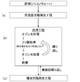
- FIG. 1 is a process flow diagram showing an embodiment of a silicon wafer evaluation method of the present invention.
- the silicon wafer to be evaluated is not particularly limited, but a mirror-polished silicon wafer is preferable. If a silicon wafer after mirror polishing is used, defects caused by polishing such as PID (Polishing Induced Defect) can be evaluated, and the quality of polishing can be evaluated.
- PID Polyishing Induced Defect
- a front surface defect measurement step of performing surface defect measurement in advance on the silicon wafer to be evaluated is performed (FIG. 1 (a)).
- it can be performed using Surfscan SP5 manufactured by KLA-Tencor. Since the processing defects hardly have a particle size larger than 40 nm, a measured particle size of 40 nm or less is sufficient.
- a cleaning step is performed by alternately repeating the oxidation treatment with ozone water and the oxide film removal treatment with hydrofluoric acid under the condition that the oxide film formed on the surface of the silicon wafer is not completely removed (FIG. 1 (b)) . It is preferable to perform this washing step with a single wafer type washing apparatus.
- the cleaning step (b) is a step of eliciting processing defects such as polishing.
- the conventional SC1-RT method (for example, JP-A-2000-208578) or the conventional quality evaluation method for wafers by ozone water and HF processing can not evaluate processing defects such as polishing, but in the present invention, By performing cleaning repeatedly by using ozone water and hydrofluoric acid without completely removing the oxide film, it is possible to reveal and evaluate only defects caused by processing without revealing defects caused by crystals. It becomes possible. In addition, cleaning can be performed without deteriorating the surface roughness of the wafer, and measurement with a small particle diameter is possible.
- the reason why only processing defects such as polishing can be revealed without revealing defects caused by crystals in the cleaning step (b) in the present invention is as follows.
- the processing defects are distorted layers in the wafer at the time of processing such as polishing and become a deteriorated layer.
- the oxide film of the wafer is removed by hydrofluoric acid, but the oxide film in the process-deteriorated area has an etching rate different from that of the surrounding oxide film, and it is manifested by alternately repeating the treatment with ozone water and the treatment with hydrofluoric acid.
- the etching amount can be reduced by repeating the ozone water and hydrofluoric acid treatment without removing the oxide film completely, so that the oxide film is always left and the crystal defects such as oxygen precipitates and metals can be reduced. It does not reveal defects such as pits due to contamination.
- the conventional quality evaluation method for wafers by ozone water and HF treatment includes the step of removing (stripping) all natural oxide films, and by completely removing the oxide films using ozone water and hydrofluoric acid. It is possible to evaluate without deteriorating the surface roughness, but with this method, crystal defects also become apparent when the natural oxide film is removed by HF.
- the ozone concentration of the ozone water in the present invention is not particularly limited, but is preferably 5 ppm to 30 ppm. In order to form a natural oxide film, the concentration is preferably 5 ppm or more, and preferably 30 ppm or less from the viewpoint of substantially practical concentration. Moreover, it is preferable to set the processing time by ozone water per time to 10 seconds or more, in order to produce
- the concentration of hydrofluoric acid is not particularly limited, but preferably 0.1 to 1.0%. If it is 0.1% or more, it is preferable because concentration control can be performed accurately. Further, in order to control the film thickness of the natural oxide film, it is preferable to be 1.0% or less.
- the hydrofluoric acid treatment time per one operation is preferably about 2 seconds to 20 seconds. If it is 2 seconds or more, the hydrofluoric acid supplied to the wafer is common, and if it is 20 seconds or less, it is preferable because the oxide film can be surely removed and the oxide film removing process can be performed.
- the number of repetitions of the oxidation treatment with ozone water and the oxide film removal treatment with hydrofluoric acid is preferably about 5 to 50 times. If the number of repetitions is five or more, processing defects can be made to appear reliably. Moreover, if it is 50 times or less, since a washing
- the number of only increased defects relative to the defects measured in the front surface defect measuring step (a) is measured.
- the measurement can be performed, for example, using the KLA-Tencor Surfscan SP5 in the same manner as in the front surface defect measurement step, and performing the same point coordinate measurement to measure the increased number of only the increased defects.
- the cleaning step (b) and the increase defect measuring step (c) are performed again. This is performed a plurality of times, and the silicon wafer is evaluated based on the measurement results of the increase defects after each cleaning step, for example, the increase tendency (inclination) of the increase defects or the increase amount of the increase defects.
- the cleaning step (b) and the increase defect measurement step (c) are alternately performed a plurality of times, and the silicon wafer is evaluated based on the measurement result of the increase defect (the inclination of the increase defect or the number of increase defects). Only processing defects such as polishing can be evaluated, excluding crystal-induced defects and particles generated in cleaning and the like.
- the deterioration of the surface roughness of the wafer and the adhesion of particles and the like are suppressed only by repeatedly performing cleaning without completely removing the oxide film using ozone water and hydrofluoric acid. Instead, only processing defects such as polishing can be revealed without revealing defects caused by crystals. Further, by observing the increasing tendency of the increased defects measured after each cleaning step, it is possible to evaluate only defects caused by processing such as polishing excluding particles caused by crystal-induced defects and particles generated by cleaning and the like. In addition, it has become possible to evaluate defects in micro areas that have never been available.
- the evaluation method of the above-mentioned silicon wafer can be applied to a method of mirror-polishing the silicon wafer before mirror-polishing to produce a silicon wafer as a product.
- this method of manufacturing a silicon wafer before manufacturing a silicon wafer to be a product, an experiment according to the evaluation method of the silicon wafer is performed on the experimental silicon wafer to specify in advance mirror polishing conditions in mirror polishing. Mirror polishing is performed under specified mirror polishing conditions to manufacture a silicon wafer as a product.
- the silicon wafer is manufactured as follows.
- a test silicon wafer before mirror polishing is prepared.
- mirror polishing is performed on the experimental silicon wafer before mirror polishing under predetermined mirror polishing conditions.
- the front surface defect measurement step, the cleaning step, and the increase defect measurement step are performed on the experimental silicon wafer thus mirror-polished in the same manner as the silicon wafer evaluation method described above (FIG. 1 (a) c) see Specifically, each process is performed as follows. First, a front surface defect measurement step of performing surface defect measurement in advance is performed on the experimental silicon wafer subjected to mirror polishing.
- the oxidation treatment with ozone water and the oxide film removal treatment with hydrofluoric acid under the condition that the oxide film formed on the surface of the experimental silicon wafer is not completely removed are alternately repeated. Perform the washing process.
- surface defect measurement is performed on the experimental silicon wafer after the cleaning step, and an increase defect measurement step is performed to measure an increase defect of the defects measured in the front surface defect measurement step.
- the above cleaning step and the increase defect measuring step are alternately repeated plural times, and the experimental silicon wafer is evaluated based on the measurement result of the increase defect after each cleaning step. Furthermore, based on the evaluation of the experimental silicon wafer, mirror-polishing conditions in mirror-polishing such that the polishing quality after mirror-polishing the silicon wafer before mirror-polishing becomes desired polishing quality are specified. Under the mirror polishing conditions specified here, the silicon wafer before mirror polishing is mirror-polished to manufacture a silicon wafer as a product.
- the slope of the increase in increased defects is small even if the cleaning step (b) and the increase defect measurement step (c) are repeated. , The number of increased defects is small.
- the quality of the polishing process is poor, defects resulting from the processing occur, so if the cleaning and the surface defect measurement are repeated, the inclination of the increase in the increase of defects increases and the number of increase defects increases.
- mirror polishing conditions should be set so that the number of defects increasing per 10 repetitions of hydrofluoric acid ⁇ ozone water in the flow shown in FIG. 1 averages 10 or less, 5 or less, or 1 or less. Can.
- the front surface defect measurement was performed using the silicon wafer which was finally polished under different polishing conditions (polishing conditions 1 to 4) and the cleaning was completed (FIG. 1 (a)).
- the wafer whose front surface defect was measured was cleaned by alternately repeating the oxidation treatment with ozone water and the oxide film removal treatment with hydrofluoric acid (FIG. 1 (b)).
- the cleaning conditions are: ozone water concentration 10 ppm, ozone water treatment time per time 20 seconds, hydrofluoric acid concentration 0.3%, hydrofluoric acid treatment time per time 5 seconds, and the flow shown in FIG. Washing was performed with the number of repetitions of ozone water being five times, and then dried. In any hydrofluoric acid treatment, the oxide film was removed while leaving the thickness on the wafer surface.
- the total number of repetitions of treatment with ozone water ⁇ treatment with hydrofluoric acid and the number of increased defects are summarized in Table 1 with the number of defects increased as the number of increased defects with respect to the result of front surface defect measurement after each cleaning step. Indicated.
- the relationship between the total number of repetitions of the treatment with ozone water ⁇ the treatment with hydrofluoric acid and the number of increased defects is plotted in a graph in FIG. Based on Table 1 and FIG. 2, the increase slope of the increase defect or the increase amount of the defect was evaluated.
- the slope of the increase in the increase in defects is different for each of the polishing conditions, and since the slope of the increase in the polishing condition 1 is almost zero, defects due to processing occur. It was found that the polishing quality was good. In addition, it was found that the polishing quality is worse for polishing conditions 2 to 4, as the increase inclination is larger, that is, polishing condition 4, polishing condition 3 and polishing condition 2 in this order.
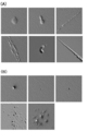
- the silicon wafer was evaluated by the evaluation method according to the SC1-RT method described in JP-A-2000-208578. Specifically, using a processing solution consisting of ammonia, hydrogen peroxide and water, the silicon wafer surface was etched to detect defects. However, it was the particles and crystal defects mainly as shown in FIG. 3 (B) that were detected by the processing. Further, even if Surfscan SP5 manufactured by KLA-Tencor Co., Ltd. was used, measurement could not be made at particle sizes of 19 nm or more because the surface roughness was deteriorated.
- the present invention is not limited to the above embodiment.
- the above embodiment is an exemplification, and it has substantially the same configuration as the technical idea described in the claims of the present invention, and any one having the same function and effect can be used. It is included in the technical scope of the invention.
Landscapes
- Chemical & Material Sciences (AREA)
- Chemical Kinetics & Catalysis (AREA)
- General Chemical & Material Sciences (AREA)
- Testing Or Measuring Of Semiconductors Or The Like (AREA)
- Cleaning Or Drying Semiconductors (AREA)
Abstract
本発明は、シリコンウェーハの評価方法であって、前記シリコンウェーハに対して、予め表面欠陥測定をする前表面欠陥測定工程と、前記シリコンウェーハに対して、オゾン水による酸化処理と、前記シリコンウェーハ表面に形成されている酸化膜を完全に除去しない条件でのフッ酸による酸化膜除去処理とを交互に繰り返す洗浄工程と、該洗浄工程後の前記シリコンウェーハに対して表面欠陥測定を行い、前記前表面欠陥測定工程で測定された欠陥に対して増加した増加欠陥を測定する増加欠陥測定工程とを有し、前記洗浄工程と前記増加欠陥測定工程を交互に複数回繰り返し行い、各洗浄工程後の前記増加欠陥の測定結果に基づいて前記シリコンウェーハを評価することを特徴とするシリコンウェーハの評価方法である。これにより、結晶起因の欠陥や洗浄等で発生するパーティクル等を除いた、研磨等の加工起因の欠陥のみを評価することができるシリコンウェーハの評価方法が提供される。
Description
本発明は、シリコンウェーハの評価方法及びシリコンウェーハの製造方法に関する。
研磨後のウェーハ品質は日々改善しており、研磨洗浄後のウェーハの品質を確認する上で、確認された異常が研磨起因、洗浄起因、又は結晶起因のものかを切り分けることが難しくなってきている。
現在、研磨状態の品質を評価するには、大量のウェーハを研磨して品質のトレンドを追うしか方法がなく、その品質の差が様々な外的要因により変わってしまうため評価が難しい。また、従来は、研磨後のウェーハを一回測定するだけであり、膨大な量のウェーハを製造するなかで従来のように抜き取り検査を行っても、研磨品質の異常を検出することは非常に難しかった。また異常値がはっきりと分かる段階では既に手遅れになることが多かった。
従来からある表面品質の評価方法としてSC1-RT法があるが、これはシリコン結晶起因の欠陥や金属汚染の評価を行うための方法であり、研磨等の加工起因の欠陥(加工欠陥)を評価する方法ではなかった(特許文献1)。
また、SC1-RT法はアルカリ水溶液を使用しているため、原理上Si、SiO2ともにエッチングを行ってしまうためウェーハ表面粗さの悪化が著しい。
また、従来のオゾン水とHF処理によるウェーハの品質評価方法は、自然酸化膜を全て除去する(剥離する)工程を含んでおり(特許文献2)、このように酸化膜の完全除去を行ってしまうと、結晶起因の欠陥の顕在化が起きてしまい、研磨等の加工欠陥を評価することができなかった。
本発明は、上記問題点に鑑みてなされたものであって、結晶起因の欠陥や洗浄等で発生するパーティクル等を除いた、研磨等の加工起因の欠陥のみを評価することができるシリコンウェーハの評価方法を提供することを目的とする。
上記課題を解決するために、本発明は、シリコンウェーハの評価方法であって、
前記シリコンウェーハに対して、予め表面欠陥測定をする前表面欠陥測定工程と、
前記シリコンウェーハに対して、オゾン水による酸化処理と、前記シリコンウェーハ表面に形成されている酸化膜を完全に除去しない条件でのフッ酸による酸化膜除去処理とを交互に繰り返す洗浄工程と、
該洗浄工程後の前記シリコンウェーハに対して表面欠陥測定を行い、前記前表面欠陥測定工程で測定された欠陥に対して増加した増加欠陥を測定する増加欠陥測定工程とを有し、
前記洗浄工程と前記増加欠陥測定工程を交互に複数回繰り返し行い、各洗浄工程後の前記増加欠陥の測定結果に基づいて前記シリコンウェーハを評価することを特徴とするシリコンウェーハの評価方法を提供する。
前記シリコンウェーハに対して、予め表面欠陥測定をする前表面欠陥測定工程と、
前記シリコンウェーハに対して、オゾン水による酸化処理と、前記シリコンウェーハ表面に形成されている酸化膜を完全に除去しない条件でのフッ酸による酸化膜除去処理とを交互に繰り返す洗浄工程と、
該洗浄工程後の前記シリコンウェーハに対して表面欠陥測定を行い、前記前表面欠陥測定工程で測定された欠陥に対して増加した増加欠陥を測定する増加欠陥測定工程とを有し、
前記洗浄工程と前記増加欠陥測定工程を交互に複数回繰り返し行い、各洗浄工程後の前記増加欠陥の測定結果に基づいて前記シリコンウェーハを評価することを特徴とするシリコンウェーハの評価方法を提供する。
このようなシリコンウェーハの評価方法であれば、洗浄工程で結晶起因の欠陥を顕在化させずに加工欠陥のみを顕在化させることができ、各洗浄工程後に測定される増加欠陥の増加傾向を見ることで、結晶起因の欠陥や洗浄等で発生するパーティクル等を除いた加工欠陥のみを評価することが可能となり、研磨等の加工品質を評価することができる。
またこの場合、前記酸化膜を完全に除去しない条件でのフッ酸による酸化膜除去処理を、フッ酸濃度0.1~1.0%とし、処理時間を2秒~20秒として行うことが好ましい。
このようなフッ酸による酸化膜除去処理とすれば、自然酸化膜厚さを制御することができるため、より確実に、酸化膜を完全に除去せずに、酸化膜除去を行うことができる。
またこの場合、前記洗浄工程を、前記オゾン水による酸化処理と前記フッ酸による酸化膜除去処理とを交互に5回以上繰り返して行うことが好ましい。
このように、オゾン水による酸化処理とフッ酸による酸化膜除去処理を5回以上繰り返すことにより、確実に、加工欠陥を顕在化させることができるので、より正確に加工品質を評価することができる。
またこの場合、前記シリコンウェーハとして、鏡面研磨後のものを用いることが好ましい。
本発明のシリコンウェーハの評価方法では、鏡面研磨後のシリコンウェーハを用いることで、研磨品質の評価を行うことができる。
また、本発明のシリコンウェーハの評価方法では、前記各洗浄工程後の前記増加欠陥の測定結果に基づいて、前記シリコンウェーハの加工起因の欠陥を評価することができる。
本発明のシリコンウェーハの評価方法では、洗浄工程で研磨等の加工欠陥のみを顕在化させることができ、また各洗浄工程後に測定される増加欠陥の増加傾向を見ることで、加工起因の欠陥のみを評価することができるため、加工品質の評価をすることが可能である。
また、本発明は、鏡面研磨前のシリコンウェーハに対して鏡面研磨を行って製品となるシリコンウェーハを製造する方法であって、
鏡面研磨前の実験用シリコンウェーハを準備する工程と、
前記鏡面研磨前の実験用シリコンウェーハに対して、所定の鏡面研磨条件で鏡面研磨を行う工程と、
前記実験用シリコンウェーハに対して、予め表面欠陥測定をする前表面欠陥測定工程と、
前記実験用シリコンウェーハに対して、オゾン水による酸化処理と、前記実験用シリコンウェーハ表面に形成されている酸化膜を完全に除去しない条件でのフッ酸による酸化膜除去処理とを交互に繰り返す洗浄工程と、
該洗浄工程後の前記実験用シリコンウェーハに対して表面欠陥測定を行い、前記前表面欠陥測定工程で測定された欠陥に対して増加した増加欠陥を測定する増加欠陥測定工程とを有し、
前記洗浄工程と前記増加欠陥測定工程を交互に複数回繰り返し行い、各洗浄工程後の前記増加欠陥の測定結果に基づいて前記実験用シリコンウェーハを評価し、
前記実験用シリコンウェーハの評価に基づいて、前記鏡面研磨前のシリコンウェーハに対して鏡面研磨を行った後の研磨品質が所望の研磨品質となるような前記鏡面研磨における鏡面研磨条件を特定し、
前記特定した鏡面研磨条件で、前記鏡面研磨前のシリコンウェーハに対して鏡面研磨を行って前記製品となるシリコンウェーハを製造することを特徴とするシリコンウェーハの製造方法を提供する。
鏡面研磨前の実験用シリコンウェーハを準備する工程と、
前記鏡面研磨前の実験用シリコンウェーハに対して、所定の鏡面研磨条件で鏡面研磨を行う工程と、
前記実験用シリコンウェーハに対して、予め表面欠陥測定をする前表面欠陥測定工程と、
前記実験用シリコンウェーハに対して、オゾン水による酸化処理と、前記実験用シリコンウェーハ表面に形成されている酸化膜を完全に除去しない条件でのフッ酸による酸化膜除去処理とを交互に繰り返す洗浄工程と、
該洗浄工程後の前記実験用シリコンウェーハに対して表面欠陥測定を行い、前記前表面欠陥測定工程で測定された欠陥に対して増加した増加欠陥を測定する増加欠陥測定工程とを有し、
前記洗浄工程と前記増加欠陥測定工程を交互に複数回繰り返し行い、各洗浄工程後の前記増加欠陥の測定結果に基づいて前記実験用シリコンウェーハを評価し、
前記実験用シリコンウェーハの評価に基づいて、前記鏡面研磨前のシリコンウェーハに対して鏡面研磨を行った後の研磨品質が所望の研磨品質となるような前記鏡面研磨における鏡面研磨条件を特定し、
前記特定した鏡面研磨条件で、前記鏡面研磨前のシリコンウェーハに対して鏡面研磨を行って前記製品となるシリコンウェーハを製造することを特徴とするシリコンウェーハの製造方法を提供する。
このようなシリコンウェーハの製造方法であれば、実験用シリコンウェーハについて洗浄工程で結晶起因の欠陥を顕在化させずに加工欠陥のみを顕在化させることができ、各洗浄工程後に測定される増加欠陥の増加傾向を見ることで、結晶起因の欠陥や洗浄等で発生するパーティクル等を除いた加工欠陥のみを評価することが可能となる。この実験により、鏡面研磨前のシリコンウェーハに対して、どのような鏡面研磨条件で鏡面研磨を行えば、所望の研磨品質が得られるかを特定することができる。そのように特定した鏡面研磨条件でシリコンウェーハを製造することにより、所望の研磨品質を有する鏡面研磨シリコンウェーハを製造することができる。
本発明のシリコンウェーハの評価方法では、洗浄工程で結晶起因の欠陥を顕在化させずに加工欠陥のみを顕在化させることができ、また、各洗浄工程後に測定される増加欠陥の増加傾向を見ることで、結晶起因の欠陥や洗浄等で発生するパーティクル等を除いた、研磨等による加工欠陥のみを評価することができる。また、本発明ではウェーハの表面粗さを悪化させずに洗浄を行うことができ、微小粒径での測定が可能となる。また、本発明のシリコンウェーハの製造方法では、加工欠陥のみを評価した実験用シリコンウェーハの評価に基づいて鏡面研磨条件を特定することにより、所望の研磨品質を有する鏡面研磨シリコンウェーハを製造することができる。
上述したように、従来のシリコンウェーハの評価方法では、結晶起因の欠陥の顕在化が起きてしまい、研磨等の加工欠陥を評価することができないという問題があった。
そして、本発明者らは上記の問題を解決するために鋭意検討を重ねた結果、オゾン水による酸化処理と、シリコンウェーハ表面に形成されている酸化膜を完全に除去しない条件でのフッ酸による酸化膜除去処理とを交互に繰り返す洗浄工程と、該洗浄工程後の前記シリコンウェーハに対して表面欠陥測定を行い、前表面欠陥測定工程で測定された欠陥に対して増加した増加欠陥を測定する増加欠陥測定工程とを交互に複数回繰り返し、各洗浄工程後の増加欠陥の測定結果に基づいてシリコンウェーハを評価すれば、洗浄工程で結晶起因の欠陥を顕在化させずに加工起因の欠陥のみを顕在化させることができ、研磨等の加工起因の欠陥のみを評価することができることを見出し、本発明に到達した。
即ち、本発明は、シリコンウェーハの評価方法であって、
前記シリコンウェーハに対して、予め表面欠陥測定をする前表面欠陥測定工程と、
前記シリコンウェーハに対して、オゾン水による酸化処理と、前記シリコンウェーハ表面に形成されている酸化膜を完全に除去しない条件でのフッ酸による酸化膜除去処理とを交互に繰り返す洗浄工程と、
該洗浄工程後の前記シリコンウェーハに対して表面欠陥測定を行い、前記前表面欠陥測定工程で測定された欠陥に対して増加した増加欠陥を測定する増加欠陥測定工程とを有し、
前記洗浄工程と前記増加欠陥測定工程を交互に複数回繰り返し行い、各洗浄工程後の前記増加欠陥の測定結果に基づいて前記シリコンウェーハを評価することを特徴とするシリコンウェーハの評価方法を提供する。
前記シリコンウェーハに対して、予め表面欠陥測定をする前表面欠陥測定工程と、
前記シリコンウェーハに対して、オゾン水による酸化処理と、前記シリコンウェーハ表面に形成されている酸化膜を完全に除去しない条件でのフッ酸による酸化膜除去処理とを交互に繰り返す洗浄工程と、
該洗浄工程後の前記シリコンウェーハに対して表面欠陥測定を行い、前記前表面欠陥測定工程で測定された欠陥に対して増加した増加欠陥を測定する増加欠陥測定工程とを有し、
前記洗浄工程と前記増加欠陥測定工程を交互に複数回繰り返し行い、各洗浄工程後の前記増加欠陥の測定結果に基づいて前記シリコンウェーハを評価することを特徴とするシリコンウェーハの評価方法を提供する。
以下、本発明のシリコンウェーハの評価方法を説明する。図1は、本発明のシリコンウェーハの評価方法の一実施形態を示す工程フロー図である。
評価対象となるシリコンウェーハとしては、特に限定されないが、鏡面研磨後のシリコンウェーハが好ましい。鏡面研磨後のシリコンウェーハを用いれば、PID(Polishing Induced Defect)等の研磨起因の欠陥を評価することができ、研磨品質の評価を行うことができる。
まず、評価するシリコンウェーハに対して予め表面欠陥測定をする前表面欠陥測定工程を行う(図1(a))。例えば、KLA-Tencor社製Surfscan SP5を用いて行うことができる。加工欠陥は40nmより大きな粒径はほとんどないため、測定粒径は40nm以下で十分である。
次いで、オゾン水による酸化処理と、シリコンウェーハ表面に形成されている酸化膜を完全に除去しない条件でのフッ酸による酸化膜除去処理とを交互に繰り返す洗浄工程を行う(図1(b))。この洗浄工程は、枚葉式洗浄装置で行うことが好ましい。
洗浄工程(b)は、研磨等の加工欠陥を顕在化させる工程である。酸化膜を完全に除去せずにフッ酸による酸化膜除去と、オゾン水によるウェーハ表面の再酸化を行うことによって、結晶起因の欠陥を顕在化させずに、研磨等の加工欠陥のみを顕在化させることができる。
従来のSC1-RT法(例えば、特開2000-208578号公報)や、従来のオゾン水とHF処理によるウェーハの品質評価方法では、研磨等の加工欠陥を評価することはできないが、本発明では酸化膜を完全に除去しないで、オゾン水とフッ酸を用いた繰り返しによる洗浄を行うことによって、結晶起因の欠陥を顕在化させずに、加工起因の欠陥のみを顕在化させて評価することが可能となる。また、ウェーハの表面粗さを悪化させずに洗浄を行うことができ、微小粒径での測定が可能となる。
このように研磨等の加工欠陥のみを顕在化させることで、加工欠陥のみを評価することが可能となる。
尚、本発明における洗浄工程(b)で結晶起因の欠陥を顕在化させずに、研磨等の加工欠陥のみを顕在させることができる理由は以下の通りである。加工欠陥は、研磨等の加工時にウェーハにひずみが発生し変質層となっている。フッ酸によってウェーハの酸化膜は除去されるが、加工変質層の部分の酸化膜は周りの酸化膜と異なるエッチングレートとなり、オゾン水による処理とフッ酸による処理とを交互に繰り返し行うことで顕在化していく。これは、フッ酸による酸化膜を残すエッチング処理を行うことによって、加工変質層と周りの箇所の酸化膜厚さに差が生じ(加工変質層の部分の酸化膜が厚い)、オゾン水により酸化膜を再形成させる(酸化膜厚さを均一に戻す)処理を繰り返し行うことによって、より差が顕著になっていくためである。酸化膜を完全に除去した場合、加工変質層の酸化膜部分も除去されてしまうために繰り返しオゾン水処理とフッ酸処理を行っても酸化膜がないために酸化膜厚さに差が生じず顕在化が起きなくなり、加工起因の欠陥評価が不可能となる。
また、本発明のように酸化膜を完全に除去せずに、オゾン水とフッ酸処理を繰り返し行うことで、エッチング量を少なくし酸化膜を常に残すことで酸素析出物などの結晶欠陥や金属汚染によるピットなどの欠陥を顕在化させることはない。
一方、従来のSC1-RT法では、エッチングを多量に行うことによる顕在化で、加工欠陥だけではなく酸素析出物などの結晶欠陥も顕在化させることとなる。
また、従来のオゾン水とHF処理によるウェーハの品質評価方法は自然酸化膜を全て除去する(剥離する)工程を含んでおり、オゾン水とフッ酸を用いて酸化膜を完全に除去することで表面粗さを悪化させずに評価することは可能であるが、この手法ではHFにより自然酸化膜を除去する際に結晶欠陥も顕在化してしまう。
本発明におけるオゾン水のオゾン濃度は特に限定されないが、5ppm~30ppmとすることが好ましい。自然酸化膜を生成するためには5ppm以上とすることが好ましく、実質的実行濃度の観点からは、30ppm以下とすることが好ましい。また、1回当たりのオゾン水による処理時間は、自然酸化膜を生成するためには10秒以上の時間とすることが好ましい。
フッ酸濃度は特に限定されないが、0.1~1.0%とすることが好ましい。0.1%以上であれば、濃度制御を正確に行うことができるために好ましい。また、自然酸化膜の膜厚を制御するためには、1.0%以下とすることが好ましい。また、1回当たりのフッ酸処理時間は2秒~20秒程度が好ましい。2秒以上であれば、ウェーハへ供給されたフッ酸が行き渡り、20秒以下であれば、確実に酸化膜を残して酸化膜除去処理を行うことができるために好ましい。
オゾン水による酸化処理と、フッ酸による酸化膜除去処理の繰り返し回数は、5回~50回程度が好ましい。繰り返し回数が5回以上であれば、確実に加工欠陥を顕在化させることができる。また、50回以下であれば、洗浄工程時間を抑えることができ、スループットが上がるため好ましい。さらに、50回以下であれば、シリコンウェーハの表面粗さを悪化させることなく評価ができるために好ましい。また、50回より多く繰り返さずとも、ウェーハの加工品質傾向を把握することができるために十分である。
次いで、洗浄工程(b)後のシリコンウェーハに対して表面欠陥測定を行い、前表面欠陥測定工程(a)で測定された欠陥に対して増加した増加欠陥を測定する増加欠陥測定工程(c)を行う。
この増加欠陥測定工程(c)では、前表面欠陥測定工程(a)で測定された欠陥に対する増加した欠陥のみの数を測定する。測定は、例えば、前表面欠陥測定工程と同様にKLA-Tencor社製Surfscan SP5を用い、同点座標測定を行うことで、増加した欠陥のみの増加数を測定することができる。
その後、再度洗浄工程(b)と増加欠陥測定工程(c)を行う。これを複数回行い、各洗浄工程後の増加欠陥の測定結果、例えば、増加欠陥の増加傾向(傾き)、又は、増加欠陥の増加量に基づいて、シリコンウェーハを評価する。
このように、洗浄工程(b)と増加欠陥測定工程(c)とを交互に複数回行い、増加欠陥の測定結果(増加欠陥の傾きまたは増加欠陥数)に基づいてシリコンウェーハを評価することで、結晶起因の欠陥や洗浄等で発生するパーティクル等を除いた、研磨等の加工欠陥のみを評価することができる。
研磨等の加工条件の良好なものでは、加工起因の欠陥は発生しない(少ない)ので洗浄工程(b)と増加欠陥測定工程(c)を繰り返しても、増加欠陥の増加の傾きは小さく、増加欠陥数は少ない。一方で、研磨加工品質が悪いと、加工起因の欠陥が発生するので洗浄と表面欠陥測定を繰り返すと増加欠陥の増加の傾きが大きくなり増加欠陥数は多くなる。この傾き又は増加欠陥数に基づいて研磨加工品質を評価することで、その時点での加工状態を確認することができる。
即ち、増加欠陥の線形近似をとった時、傾きの大きいもの、又は増加欠陥数が大きいものほど、潜在的な加工欠陥を含んでおり、加工品質が悪いこととなる。
以上のように、本発明では、オゾン水とフッ酸を用いて酸化膜を完全に除去せずに洗浄を繰り返し行う事によって、ウェーハの表面粗さの悪化やパーティクル等の付着を抑制するだけでなく、結晶起因の欠陥を顕在化させずに、研磨等の加工欠陥のみを顕在化させることができる。また、各洗浄工程後に測定される増加欠陥の増加傾向を見ることで、結晶起因の欠陥や洗浄等で発生するパーティクル等を除いた、研磨等の加工起因の欠陥のみを評価することができる。また今までにない微小領域での欠陥評価が可能になった。
また、上記のシリコンウェーハの評価方法は、鏡面研磨前のシリコンウェーハに対して鏡面研磨を行って製品となるシリコンウェーハを製造する方法に応用することができる。このシリコンウェーハの製造方法では、製品となるシリコンウェーハを製造する前に、実験用シリコンウェーハに対して上記シリコンウェーハの評価方法に沿った実験を行って、鏡面研磨における鏡面研磨条件を予め特定し、特定した鏡面研磨条件で鏡面研磨を行って製品となるシリコンウェーハの製造を行う。具体的には、以下のようにしてシリコンウェーハの製造を行う。
まず、鏡面研磨前の実験用シリコンウェーハを準備する。次に、この鏡面研磨前の実験用シリコンウェーハに対して、所定の鏡面研磨条件で鏡面研磨を行う。このようにして鏡面研磨を行った実験用シリコンウェーハに対して、上記のシリコンウェーハの評価方法と同様、前表面欠陥測定工程、洗浄工程、増加欠陥測定工程を行う(図1(a)~(c)参照)。具体的には、以下のように各工程を行う。まず、鏡面研磨を行った実験用シリコンウェーハに対して、予め表面欠陥測定をする前表面欠陥測定工程を行う。次に、実験用シリコンウェーハに対して、オゾン水による酸化処理と、実験用シリコンウェーハ表面に形成されている酸化膜を完全に除去しない条件でのフッ酸による酸化膜除去処理とを交互に繰り返す洗浄工程を行う。次に、洗浄工程後の実験用シリコンウェーハに対して表面欠陥測定を行い、前表面欠陥測定工程で測定された欠陥に対して増加した増加欠陥を測定する増加欠陥測定工程を行う。
上記の洗浄工程と増加欠陥測定工程を交互に複数回繰り返し行い、各洗浄工程後の増加欠陥の測定結果に基づいて実験用シリコンウェーハを評価する。さらに、この実験用シリコンウェーハの評価に基づいて、鏡面研磨前のシリコンウェーハに対して鏡面研磨を行った後の研磨品質が所望の研磨品質となるような鏡面研磨における鏡面研磨条件を特定する。ここで特定した鏡面研磨条件で、鏡面研磨前のシリコンウェーハに対して鏡面研磨を行って製品となるシリコンウェーハを製造する。
鏡面研磨後の加工欠陥が発生しない(少ない)研磨条件で研磨された鏡面研磨シリコンウェーハは、洗浄工程(b)と増加欠陥測定工程(c)を繰り返しても、増加欠陥の増加の傾きは小さく、増加欠陥数は少ない。一方で、研磨加工品質が悪いと、加工起因の欠陥が発生するので洗浄と表面欠陥測定を繰り返すと増加欠陥の増加の傾きが大きくなり増加欠陥数は多くなる。この傾き又は増加欠陥数に基づいて実験用シリコンウェーハにおける研磨加工品質を評価することで、鏡面研磨前のシリコンウェーハに対して、どのような鏡面研磨条件で鏡面研磨を行えば、所望の研磨品質が得られるかを特定することができる。
より具体的には、増加欠陥の線形近似をとった時、傾きがないか小さくなるような鏡面研磨条件を選ぶことができる。例えば、図1に示すフローでフッ酸→オゾン水の繰り返し回数10回辺り増加欠陥数が平均して10個以下、5個以下、又は1個以下になるようにして鏡面研磨条件を設定することができる。
以下、実施例及び比較例を示して本発明をより具体的に説明するが、本発明はこれらの実施例に限定されるものではない。
(実施例)
異なる研磨条件(研磨条件1~4)で最終研磨され、洗浄が終了したシリコンウェーハを用いて、前表面欠陥測定を行った(図1(a))。前表面欠陥測定を行ったウェーハに対して、オゾン水による酸化処理とフッ酸による酸化膜除去処理とを交互に繰り返すことによって洗浄を行った(図1(b))。
異なる研磨条件(研磨条件1~4)で最終研磨され、洗浄が終了したシリコンウェーハを用いて、前表面欠陥測定を行った(図1(a))。前表面欠陥測定を行ったウェーハに対して、オゾン水による酸化処理とフッ酸による酸化膜除去処理とを交互に繰り返すことによって洗浄を行った(図1(b))。
洗浄条件は、オゾン水濃度10ppm、1回当たりのオゾン水処理時間を20秒、フッ酸濃度0.3%、1回当たりのフッ酸処理時間5秒とし、図1に示すフローでフッ酸→オゾン水の繰り返し回数を5回として洗浄を行い、その後乾燥した。尚、いずれのフッ酸処理も、ウェーハ表面に厚さを残して酸化膜除去を行った。
次いで、洗浄工程後のシリコンウェーハに対して表面欠陥測定を行い、前表面欠陥測定工程(a)で測定された欠陥に対して増加した増加欠陥を測定した(図1(c))。尚、前表面欠陥測定及び増加欠陥測定は、KLA-Tencor社製Surfscan SP5を用いて粒径19nm以上で測定を行い、同点座標測定を行うことによって、増加した増加欠陥のみを測定した。
洗浄工程と増加欠陥測定工程を、オゾン水による処理→フッ酸による処理の合計繰り返し回数が50回となるまで(即ち、洗浄工程と増加欠陥測定工程の繰り返し回数が10回となるまで)、繰り返し行った。
各洗浄工程後の、前表面欠陥測定の結果に対して増加した欠陥のみの個数を増加欠陥数として、オゾン水による処理→フッ酸による処理の合計繰り返し回数と増加欠陥数をまとめて表1に示した。また、オゾン水による処理→フッ酸による処理の合計繰り返し回数と増加欠陥数との関係をグラフにプロットしたものを図2に示す。表1及び図2に基づいて、増加欠陥の増加の傾きまたは欠陥の増加量を評価した。
また、洗浄後のウェーハ表面をSEMで観察したところ、ウェーハ表面に結晶欠陥は顕在化しておらず、図3(A)に示すような加工欠陥のみが顕在化していることが判り、加工品質の評価が可能であることが判った。
図2に示されるように、研磨条件1~4では、研磨条件ごとに増加欠陥の増加の傾きが異なっており、研磨条件1は増加の傾きがほぼ無いため、加工起因の欠陥は発生していない、即ち研磨品質が良いことが判った。また、研磨条件2~4では、増加の傾きが大きいほど、即ち研磨条件4、研磨条件3、研磨条件2の順で、研磨品質が悪いことが判った。

(比較例)
特開2000-208578号に記載のSC1-RT法による評価方法で、シリコンウェーハの評価を行った。具体的には、アンモニア、過酸化水素、水よりなる処理液を用い、シリコンウェーハ表面にエッチング処理を施して欠陥を検出した。しかしながら、当該処理で検出したのは、主に図3(B)に示すようなパーティクルや結晶欠陥であった。また、KLA-Tencor社製Surfscan SP5を用いても、粒径19nm以上では表面粗さが悪化しているために、測定不可能であった。
特開2000-208578号に記載のSC1-RT法による評価方法で、シリコンウェーハの評価を行った。具体的には、アンモニア、過酸化水素、水よりなる処理液を用い、シリコンウェーハ表面にエッチング処理を施して欠陥を検出した。しかしながら、当該処理で検出したのは、主に図3(B)に示すようなパーティクルや結晶欠陥であった。また、KLA-Tencor社製Surfscan SP5を用いても、粒径19nm以上では表面粗さが悪化しているために、測定不可能であった。
なお、本発明は、上記実施形態に限定されるものではない。上記実施形態は、例示であり、本発明の特許請求の範囲に記載された技術的思想と実質的に同一な構成を有し、同様な作用効果を奏するものは、いかなるものであっても本発明の技術的範囲に包含される。
Claims (6)
- シリコンウェーハの評価方法であって、
前記シリコンウェーハに対して、予め表面欠陥測定をする前表面欠陥測定工程と、
前記シリコンウェーハに対して、オゾン水による酸化処理と、前記シリコンウェーハ表面に形成されている酸化膜を完全に除去しない条件でのフッ酸による酸化膜除去処理とを交互に繰り返す洗浄工程と、
該洗浄工程後の前記シリコンウェーハに対して表面欠陥測定を行い、前記前表面欠陥測定工程で測定された欠陥に対して増加した増加欠陥を測定する増加欠陥測定工程とを有し、
前記洗浄工程と前記増加欠陥測定工程を交互に複数回繰り返し行い、各洗浄工程後の前記増加欠陥の測定結果に基づいて前記シリコンウェーハを評価することを特徴とするシリコンウェーハの評価方法。 - 前記酸化膜を完全に除去しない条件でのフッ酸による酸化膜除去処理を、フッ酸濃度0.1~1.0%とし、処理時間を2秒~20秒として行うことを特徴とする請求項1に記載のシリコンウェーハの評価方法。
- 前記洗浄工程を、前記オゾン水による酸化処理と前記フッ酸による酸化膜除去処理とを交互に5回以上繰り返して行うことを特徴とする請求項1又は請求項2に記載のシリコンウェーハの評価方法。
- 前記シリコンウェーハとして、鏡面研磨後のものを用いることを特徴とする請求項1から請求項3のいずれか一項に記載のシリコンウェーハの評価方法。
- 前記各洗浄工程後の前記増加欠陥の測定結果に基づいて、前記シリコンウェーハの加工起因の欠陥を評価することを特徴とする請求項1から請求項4のいずれか一項に記載のシリコンウェーハの評価方法。
- 鏡面研磨前のシリコンウェーハに対して鏡面研磨を行って製品となるシリコンウェーハを製造する方法であって、
鏡面研磨前の実験用シリコンウェーハを準備する工程と、
前記鏡面研磨前の実験用シリコンウェーハに対して、所定の鏡面研磨条件で鏡面研磨を行う工程と、
前記実験用シリコンウェーハに対して、予め表面欠陥測定をする前表面欠陥測定工程と、
前記実験用シリコンウェーハに対して、オゾン水による酸化処理と、前記実験用シリコンウェーハ表面に形成されている酸化膜を完全に除去しない条件でのフッ酸による酸化膜除去処理とを交互に繰り返す洗浄工程と、
該洗浄工程後の前記実験用シリコンウェーハに対して表面欠陥測定を行い、前記前表面欠陥測定工程で測定された欠陥に対して増加した増加欠陥を測定する増加欠陥測定工程とを有し、
前記洗浄工程と前記増加欠陥測定工程を交互に複数回繰り返し行い、各洗浄工程後の前記増加欠陥の測定結果に基づいて前記実験用シリコンウェーハを評価し、
前記実験用シリコンウェーハの評価に基づいて、前記鏡面研磨前のシリコンウェーハに対して鏡面研磨を行った後の研磨品質が所望の研磨品質となるような前記鏡面研磨における鏡面研磨条件を特定し、
前記特定した鏡面研磨条件で、前記鏡面研磨前のシリコンウェーハに対して鏡面研磨を行って前記製品となるシリコンウェーハを製造することを特徴とするシリコンウェーハの製造方法。
Priority Applications (5)
| Application Number | Priority Date | Filing Date | Title |
|---|---|---|---|
| US16/642,194 US11222780B2 (en) | 2017-09-06 | 2018-08-20 | Method for evaluating silicon wafer and method for manufacturing silicon wafer |
| DE112018004122.0T DE112018004122T5 (de) | 2017-09-06 | 2018-08-20 | Verfahren zum Bewerten von Siliziumwafern und Verfahren zum Herstellen von Siliziumwafern |
| KR1020207005723A KR102560436B1 (ko) | 2017-09-06 | 2018-08-20 | 실리콘 웨이퍼의 평가방법 및 실리콘 웨이퍼의 제조방법 |
| SG11202001755PA SG11202001755PA (en) | 2017-09-06 | 2018-08-20 | Method for evaluating silicon wafer and method for manufacturing silicon wafer |
| CN201880055612.7A CN111052330B (zh) | 2017-09-06 | 2018-08-20 | 硅晶圆的评价方法及硅晶圆的制造方法 |
Applications Claiming Priority (4)
| Application Number | Priority Date | Filing Date | Title |
|---|---|---|---|
| JP2017171164 | 2017-09-06 | ||
| JP2017-171164 | 2017-09-06 | ||
| JP2018079891A JP6773070B2 (ja) | 2017-09-06 | 2018-04-18 | シリコンウェーハの評価方法及びシリコンウェーハの製造方法 |
| JP2018-079891 | 2018-04-18 |
Publications (1)
| Publication Number | Publication Date |
|---|---|
| WO2019049641A1 true WO2019049641A1 (ja) | 2019-03-14 |
Family
ID=65633856
Family Applications (1)
| Application Number | Title | Priority Date | Filing Date |
|---|---|---|---|
| PCT/JP2018/030614 Ceased WO2019049641A1 (ja) | 2017-09-06 | 2018-08-20 | シリコンウェーハの評価方法及びシリコンウェーハの製造方法 |
Country Status (2)
| Country | Link |
|---|---|
| US (1) | US11222780B2 (ja) |
| WO (1) | WO2019049641A1 (ja) |
Families Citing this family (2)
| Publication number | Priority date | Publication date | Assignee | Title |
|---|---|---|---|---|
| CN112420539A (zh) * | 2020-11-13 | 2021-02-26 | 西安奕斯伟硅片技术有限公司 | 一种硅片处理方法和硅片 |
| CN119559162A (zh) * | 2025-01-21 | 2025-03-04 | 青岛嘉星晶电科技股份有限公司 | 基于图像处理的蓝宝石晶棒抛光质量评估方法 |
Citations (3)
| Publication number | Priority date | Publication date | Assignee | Title |
|---|---|---|---|---|
| JP2003270169A (ja) * | 2002-01-09 | 2003-09-25 | Toshiba Ceramics Co Ltd | シリコンウエハの八面体ボイドの評価方法 |
| WO2012172724A1 (ja) * | 2011-06-17 | 2012-12-20 | 信越半導体株式会社 | 半導体ウェーハの洗浄方法 |
| JP2017219409A (ja) * | 2016-06-07 | 2017-12-14 | 信越半導体株式会社 | 半導体シリコンウェーハの表面欠陥検査方法 |
Family Cites Families (2)
| Publication number | Priority date | Publication date | Assignee | Title |
|---|---|---|---|---|
| JP3717691B2 (ja) | 1999-01-13 | 2005-11-16 | 信越半導体株式会社 | シリコンウェーハの評価方法 |
| JP2002353281A (ja) | 2001-05-29 | 2002-12-06 | Shin Etsu Handotai Co Ltd | シリコンウェーハ表面品質の評価方法 |
-
2018
- 2018-08-20 US US16/642,194 patent/US11222780B2/en active Active
- 2018-08-20 WO PCT/JP2018/030614 patent/WO2019049641A1/ja not_active Ceased
Patent Citations (3)
| Publication number | Priority date | Publication date | Assignee | Title |
|---|---|---|---|---|
| JP2003270169A (ja) * | 2002-01-09 | 2003-09-25 | Toshiba Ceramics Co Ltd | シリコンウエハの八面体ボイドの評価方法 |
| WO2012172724A1 (ja) * | 2011-06-17 | 2012-12-20 | 信越半導体株式会社 | 半導体ウェーハの洗浄方法 |
| JP2017219409A (ja) * | 2016-06-07 | 2017-12-14 | 信越半導体株式会社 | 半導体シリコンウェーハの表面欠陥検査方法 |
Also Published As
| Publication number | Publication date |
|---|---|
| US20200203233A1 (en) | 2020-06-25 |
| US11222780B2 (en) | 2022-01-11 |
Similar Documents
| Publication | Publication Date | Title |
|---|---|---|
| JP5029234B2 (ja) | エピタキシャルウェーハの製造方法 | |
| JP6933187B2 (ja) | 半導体シリコンウェーハの金属不純物除去方法 | |
| JP6773070B2 (ja) | シリコンウェーハの評価方法及びシリコンウェーハの製造方法 | |
| WO2013179569A1 (ja) | 半導体ウェーハの洗浄方法 | |
| WO2019049641A1 (ja) | シリコンウェーハの評価方法及びシリコンウェーハの製造方法 | |
| EP1900858A1 (en) | Epitaxial wafer and method of producing same | |
| TWI795547B (zh) | 矽晶圓的洗淨方法 | |
| KR20110036990A (ko) | 균일 산화막 형성 방법 및 세정 방법 | |
| JP6610443B2 (ja) | 半導体シリコンウェーハの表面欠陥検査方法 | |
| JP6529715B2 (ja) | シリコンウェーハの製造方法 | |
| JP6536502B2 (ja) | パーティクルカウンタ校正用ウェーハの作製方法 | |
| CN116918041A (zh) | 硅晶圆的清洗方法、硅晶圆的制造方法及硅晶圆 | |
| JP7279753B2 (ja) | シリコンウェーハの洗浄方法および製造方法 | |
| JP7582057B2 (ja) | シリコンウェーハの洗浄方法及びシリコンウェーハの製造方法 | |
| JP2007234964A (ja) | 半導体基板の洗浄方法 | |
| WO2022190830A1 (ja) | シリコンウェーハの洗浄方法、シリコンウェーハの製造方法及びシリコンウェーハ | |
| JP2985583B2 (ja) | シリコンウエーハの鏡面加工表面における加工変質層検査方法とその厚さ測定方法 | |
| JP2009182233A (ja) | アニールウェーハの洗浄方法 | |
| JP5385566B2 (ja) | 研磨クロスの金属汚染評価方法 | |
| JPH10112486A (ja) | 半導体ウェハの酸化膜耐圧特性の測定方法 | |
| CN108257885A (zh) | 物理气相沉积中钛或氮化钛颗粒控片的使用方法 |
Legal Events
| Date | Code | Title | Description |
|---|---|---|---|
| 121 | Ep: the epo has been informed by wipo that ep was designated in this application |
Ref document number: 18854097 Country of ref document: EP Kind code of ref document: A1 |
|
| 122 | Ep: pct application non-entry in european phase |
Ref document number: 18854097 Country of ref document: EP Kind code of ref document: A1 |