WO2019049191A1 - 発光デバイス、発光デバイスの製造装置 - Google Patents
発光デバイス、発光デバイスの製造装置 Download PDFInfo
- Publication number
- WO2019049191A1 WO2019049191A1 PCT/JP2017/031895 JP2017031895W WO2019049191A1 WO 2019049191 A1 WO2019049191 A1 WO 2019049191A1 JP 2017031895 W JP2017031895 W JP 2017031895W WO 2019049191 A1 WO2019049191 A1 WO 2019049191A1
- Authority
- WO
- WIPO (PCT)
- Prior art keywords
- light emitting
- emitting device
- light
- quantum dot
- emitting layer
- Prior art date
- Legal status (The legal status is an assumption and is not a legal conclusion. Google has not performed a legal analysis and makes no representation as to the accuracy of the status listed.)
- Ceased
Links
Images




Classifications
-
- H—ELECTRICITY
- H10—SEMICONDUCTOR DEVICES; ELECTRIC SOLID-STATE DEVICES NOT OTHERWISE PROVIDED FOR
- H10K—ORGANIC ELECTRIC SOLID-STATE DEVICES
- H10K50/00—Organic light-emitting devices
- H10K50/10—OLEDs or polymer light-emitting diodes [PLED]
- H10K50/11—OLEDs or polymer light-emitting diodes [PLED] characterised by the electroluminescent [EL] layers
- H10K50/12—OLEDs or polymer light-emitting diodes [PLED] characterised by the electroluminescent [EL] layers comprising dopants
- H10K50/121—OLEDs or polymer light-emitting diodes [PLED] characterised by the electroluminescent [EL] layers comprising dopants for assisting energy transfer, e.g. sensitization
-
- G—PHYSICS
- G09—EDUCATION; CRYPTOGRAPHY; DISPLAY; ADVERTISING; SEALS
- G09F—DISPLAYING; ADVERTISING; SIGNS; LABELS OR NAME-PLATES; SEALS
- G09F9/00—Indicating arrangements for variable information in which the information is built-up on a support by selection or combination of individual elements
- G09F9/30—Indicating arrangements for variable information in which the information is built-up on a support by selection or combination of individual elements in which the desired character or characters are formed by combining individual elements
-
- H—ELECTRICITY
- H05—ELECTRIC TECHNIQUES NOT OTHERWISE PROVIDED FOR
- H05B—ELECTRIC HEATING; ELECTRIC LIGHT SOURCES NOT OTHERWISE PROVIDED FOR; CIRCUIT ARRANGEMENTS FOR ELECTRIC LIGHT SOURCES, IN GENERAL
- H05B33/00—Electroluminescent light sources
- H05B33/10—Apparatus or processes specially adapted to the manufacture of electroluminescent light sources
-
- H—ELECTRICITY
- H05—ELECTRIC TECHNIQUES NOT OTHERWISE PROVIDED FOR
- H05B—ELECTRIC HEATING; ELECTRIC LIGHT SOURCES NOT OTHERWISE PROVIDED FOR; CIRCUIT ARRANGEMENTS FOR ELECTRIC LIGHT SOURCES, IN GENERAL
- H05B33/00—Electroluminescent light sources
- H05B33/12—Light sources with substantially two-dimensional [2D] radiating surfaces
-
- H—ELECTRICITY
- H05—ELECTRIC TECHNIQUES NOT OTHERWISE PROVIDED FOR
- H05B—ELECTRIC HEATING; ELECTRIC LIGHT SOURCES NOT OTHERWISE PROVIDED FOR; CIRCUIT ARRANGEMENTS FOR ELECTRIC LIGHT SOURCES, IN GENERAL
- H05B33/00—Electroluminescent light sources
- H05B33/12—Light sources with substantially two-dimensional [2D] radiating surfaces
- H05B33/14—Light sources with substantially two-dimensional [2D] radiating surfaces characterised by the chemical or physical composition or the arrangement of the electroluminescent material, or by the simultaneous addition of the electroluminescent material in or onto the light source
-
- H—ELECTRICITY
- H05—ELECTRIC TECHNIQUES NOT OTHERWISE PROVIDED FOR
- H05B—ELECTRIC HEATING; ELECTRIC LIGHT SOURCES NOT OTHERWISE PROVIDED FOR; CIRCUIT ARRANGEMENTS FOR ELECTRIC LIGHT SOURCES, IN GENERAL
- H05B33/00—Electroluminescent light sources
- H05B33/12—Light sources with substantially two-dimensional [2D] radiating surfaces
- H05B33/22—Light sources with substantially two-dimensional [2D] radiating surfaces characterised by the chemical or physical composition or the arrangement of auxiliary dielectric or reflective layers
-
- H—ELECTRICITY
- H10—SEMICONDUCTOR DEVICES; ELECTRIC SOLID-STATE DEVICES NOT OTHERWISE PROVIDED FOR
- H10K—ORGANIC ELECTRIC SOLID-STATE DEVICES
- H10K50/00—Organic light-emitting devices
- H10K50/10—OLEDs or polymer light-emitting diodes [PLED]
- H10K50/11—OLEDs or polymer light-emitting diodes [PLED] characterised by the electroluminescent [EL] layers
-
- H—ELECTRICITY
- H10—SEMICONDUCTOR DEVICES; ELECTRIC SOLID-STATE DEVICES NOT OTHERWISE PROVIDED FOR
- H10K—ORGANIC ELECTRIC SOLID-STATE DEVICES
- H10K50/00—Organic light-emitting devices
- H10K50/10—OLEDs or polymer light-emitting diodes [PLED]
- H10K50/11—OLEDs or polymer light-emitting diodes [PLED] characterised by the electroluminescent [EL] layers
- H10K50/115—OLEDs or polymer light-emitting diodes [PLED] characterised by the electroluminescent [EL] layers comprising active inorganic nanostructures, e.g. luminescent quantum dots
-
- H—ELECTRICITY
- H10—SEMICONDUCTOR DEVICES; ELECTRIC SOLID-STATE DEVICES NOT OTHERWISE PROVIDED FOR
- H10K—ORGANIC ELECTRIC SOLID-STATE DEVICES
- H10K59/00—Integrated devices, or assemblies of multiple devices, comprising at least one organic light-emitting element covered by group H10K50/00
- H10K59/80—Constructional details
- H10K59/875—Arrangements for extracting light from the devices
-
- H—ELECTRICITY
- H10—SEMICONDUCTOR DEVICES; ELECTRIC SOLID-STATE DEVICES NOT OTHERWISE PROVIDED FOR
- H10K—ORGANIC ELECTRIC SOLID-STATE DEVICES
- H10K71/00—Manufacture or treatment specially adapted for the organic devices covered by this subclass
-
- H—ELECTRICITY
- H10—SEMICONDUCTOR DEVICES; ELECTRIC SOLID-STATE DEVICES NOT OTHERWISE PROVIDED FOR
- H10K—ORGANIC ELECTRIC SOLID-STATE DEVICES
- H10K2101/00—Properties of the organic materials covered by group H10K85/00
- H10K2101/10—Triplet emission
-
- H—ELECTRICITY
- H10—SEMICONDUCTOR DEVICES; ELECTRIC SOLID-STATE DEVICES NOT OTHERWISE PROVIDED FOR
- H10K—ORGANIC ELECTRIC SOLID-STATE DEVICES
- H10K59/00—Integrated devices, or assemblies of multiple devices, comprising at least one organic light-emitting element covered by group H10K50/00
- H10K59/10—OLED displays
- H10K59/12—Active-matrix OLED [AMOLED] displays
- H10K59/122—Pixel-defining structures or layers, e.g. banks
Definitions
- the present invention relates to a light emitting device including a light emitting element including a quantum dot and an apparatus for manufacturing the light emitting device.
- Patent Document 1 describes a light emitting element provided with a light emitting layer in which a material emitting thermally activated delayed fluorescence (TADF) and a material emitting fluorescence are mixed in order to increase the light emission efficiency.
- TADF thermally activated delayed fluorescence
- a singlet excited state of the TADF material is created by the reverse intersystem crossing from the triplet excited state of the TADF material. Thereafter, the singlet excited state of the TADF material is transitioned to the singlet excited state of the fluorescent material by Forster transition to generate fluorescence.
- the energy gap between the triplet excitation level and the singlet excitation level of the TADF material is very small.
- the triplet excited state of the TADF material is easily created by the intersystem crossing from the singlet excited state of the TADF material. In this state, Dexter transition from the triplet excited state of the TADF material to the triplet excited state of the fluorescent material may occur.
- the deactivation process from the triplet excited state to the ground state of the fluorescent material is a non-emission process. For this reason, in the light emitting element of Patent Document 1, the light emission efficiency may be reduced.
- a light emitting layer in which quantum dots and a light emitting body which is a phosphor or a phosphor are dispersed, a first electrode lower than the light emitting layer, and the light emitting layer
- the light emitting device further includes a second electrode in an upper layer, wherein the emission spectrum of the quantum dot and the absorption spectrum of the light emitter overlap at least in part.
- the light emission efficiency of the light emitter can be improved.
- the direction from the light emitting layer of the light emitting device to the first electrode is referred to as “downward”, and the direction from the light emitting layer of the light emitting device to the second electrode is referred to as “upper direction”.
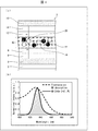
- FIG. 1A is a schematic cross-sectional view of a light emitting device 2 according to the present embodiment.
- the light emitting device 2 has a structure in which each layer is stacked on an array substrate 3 on which a TFT (Thin Film Transistor) (not shown) is formed.
- the first electrode 4 formed on the upper layer of the array substrate 3 is electrically connected to the TFT of the array substrate 3.
- the light emitting device 2 includes a hole injection layer 6, a hole transport layer 8, a light emitting layer 10, an electron transport layer 12, an electron injection layer 14, and a second electrode 16 on the first electrode 4. It prepares from the lower layer in this order.
- the first electrode 4 is an anode
- the second electrode 16 is a cathode.
- the light emitting layer 10 has a host 18, a quantum dot (semiconductor nanoparticle) 20, and a phosphor 22 as a light emitter.
- the quantum dots 20 and the phosphors 22 are dispersed in the host 18.
- the host 18 comprises a compound having the functions of injection and transport of holes and electrons.
- the host 18 may comprise a photosensitive material.
- the host 18 may further comprise a dispersion material not shown.
- holes are injected from the first electrode 4 and electrons from the second electrode 16 toward the light emitting layer 10 by applying a potential difference between the first electrode 4 and the second electrode 16. Be done. As shown in (a) of FIG. 1, holes from the first electrode 4 reach the light emitting layer 10 through the hole injection layer 6 and the hole transport layer 8. Electrons from the second electrode 16 reach the light emitting layer 10 via the electron injection layer 14 and the electron transport layer 12.
- the holes and electrons reaching the light emitting layer 10 are recombined in the quantum dot 20 through the host 18 to generate excitons.
- the hole transportability of the hole injection layer 6 and the hole transport layer 8 and the electron transportability of the electron injection layer 14 and the electron transport layer 12 are such that excitons are generated in the light emitting layer 10. It is adjusted.
- the quantum dot 20 has a valence band level and a conduction band level. When the quantum dot 20 is given energy from excitons generated by recombination of holes and electrons, excitons are excited from the valence band level of the quantum dot 20 to the conduction band level.
- the quantum dot 20 may be, for example, a semiconductor nanoparticle having a core / shell structure, with CdSe in the core and ZnS in the shell.
- the phosphor 22 has a ground level, a singlet excitation level, and a triplet excitation level, and excitons excited from the ground level to the singlet excitation level transition to the ground level. It is a fluorescent material that emits fluorescence at the same time.
- FIG. 1B is a spectrum diagram showing an example of the fluorescence spectrum of the quantum dot 20 by a solid line and an example of an absorption spectrum of the phosphor 22 by a broken line.
- the hatched portion in (b) of FIG. 1 indicates a portion where the fluorescence spectrum of the quantum dot 20 and the absorption spectrum of the phosphor 22 overlap.
- the horizontal axis represents wavelength
- the vertical axis represents normalized spectral intensity.
- Each spectrum in (b) of FIG. 1 is normalized with the maximum intensity being 1.
- FIG. 2 is a view for explaining the light emitting mechanism of the light emitting device 2 according to the present embodiment.
- the left and right molecular orbital diagrams in FIG. 2 are diagrams showing the molecular orbitals of the quantum dot 20 and the fluorescent substance 22, respectively.
- VB represents a valence band level
- CB represents a conduction band level.
- S0 represents a ground level
- S1 represents a singlet excitation level
- the triplet excitation level is not shown.
- the conduction band level of the quantum dot 20 is higher than the singlet excitation level of the phosphor 22. This corresponds to the peak wavelength of the emission spectrum of the quantum dot 20 being shorter than the peak wavelength of the emission spectrum of the phosphor 22.
- the light emitting mechanism of the light emitting device 2 according to the present embodiment will be described in detail with reference to FIGS. 1 and 2.
- excitons in the conduction band level of the quantum dot 20 transition to the singlet excitation level of the phosphor 22 by energy transfer by the Forster mechanism.
- the Forster mechanism is a mechanism in which energy transfer occurs through the resonance phenomenon of dipole oscillation between the quantum dot 20 and the phosphor 22 in the present embodiment.
- the energy transfer by the Forster mechanism does not require direct contact between the quantum dots 20 and the phosphors 22.
- the rate constant of the Forster mechanism is k h * ⁇ g
- k h * ⁇ g is expressed by the following equation (1).
- ⁇ represents a frequency.
- f ′ h ( ⁇ ) represents the normalized fluorescence spectrum of the quantum dot 20.
- ⁇ g ( ⁇ ) represents the molar absorption coefficient of the phosphor 22.
- N represents the Avogadro's number.
- n represents the refractive index of the host 18.
- R represents the intermolecular distance between the quantum dot 20 and the phosphor 22.
- ⁇ represents the fluorescence lifetime of the excited state of the quantum dot 20 to be measured.
- ⁇ represents the fluorescence quantum yield of the quantum dot 20.
- the fluorescence spectrum of the quantum dot 20 in the present embodiment and the absorption spectrum of the phosphor 22 overlap at least in part. Therefore, the above-described energy transfer occurs between the quantum dots 20 and the phosphors 22 whose intermolecular distance is sufficiently close.
- the peak wavelength of the emission spectrum of the quantum dot 20 is included in the absorption spectrum of the phosphor 22.
- the peak wavelength of the absorption spectrum of the phosphor 22 is included in the emission spectrum of the quantum dot 20. For this reason, the above-mentioned energy transfer occurs more dominantly.
- the generated excitons move from the quantum dot 20 to the phosphor 22 by energy transfer of the Forster mechanism, and fluorescence is generated in the phosphor 22.
- energy transfer from the quantum dots 20 to the phosphors 22 no Dexter transition that causes a non-emission process does not occur. For this reason, the light emitting device 2 according to the present embodiment can more efficiently obtain fluorescence from excitons that transfer energy to the phosphor 22.
- quantum dots that emit short wavelength fluorescence in the violet or ultraviolet region are easier to synthesize than thermally activated delayed phosphors. That is, a quantum dot that efficiently transfers energy to a fluorescent material having a peak of the emission spectrum in the deep-blue region is easier to synthesize as compared with a thermally activated delayed phosphor. Therefore, the light emitting device 2 according to the present embodiment can be manufactured more easily than in the past, and the fluorescence in the deep-blue region can be efficiently obtained.
- light in the violet region or ultraviolet region is light having an emission center wavelength in a wavelength band of 420 nm or less.
- the concentration of the quantum dot 20 in the light emitting layer 10 is, for example, 0.1 mass percent to 1 mass percent. If the concentration of the quantum dots 20 is within the above range, the decrease in light emission efficiency due to the concentration disappearance can be reduced, and the generation of excitons in the dispersion material can be reduced.
- the concentration of the phosphor 22 in the light emitting layer is 10% by mass to 30% by mass. If the concentration of the phosphors 22 is within the above range, the above-described energy transfer can be efficiently generated.
- the light emitting layer 10 includes the phosphor 22 as a light emitter.
- the present invention is not limited to this, and the light emitting layer 10 may include a phosphor that emits phosphorescence instead of the phosphor as a light emitter.
- energy transfer occurs from the quantum dot to the phosphor by the Forster mechanism. Thereafter, due to the intersystem crossing, the excitons transition from the singlet excitation level to the triplet excitation level of the phosphor. Phosphorescence can be obtained from the phosphor when excitons transition from the triplet excitation level to the ground level of the phosphor. Therefore, even in the above configuration, it is possible to obtain phosphorescence in the deep-blue region more efficiently.
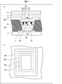
- FIG. 3 is an enlarged top view and an enlarged sectional view of the light emitting device 2 according to the present embodiment.
- FIG. 3A is a view showing the top surface of the light emitting device 2 in the vicinity of the pixel, as seen through the electron transport layer 12, the electron injection layer 14, and the second electrode 16.
- FIG. 3B is a cross-sectional view taken along line AA of FIG. 3A.
- the light emitting device 2 includes a plurality of pixel regions RP, GP, BP as compared with the previous embodiment.
- the hole injection layer 6R, the hole transport layer 8R, and the light emitting layer 10R are sequentially formed from the lower side on the first electrode 4.
- the hole injection layers 6G and 6B, the hole transport layers 8G and 8B, and the light emitting layers 10G and 10B are respectively formed in order from the lower side.
- the light emitting device 2 further includes an edge cover 24.
- the edge cover 24 has a plurality of openings and defines a plurality of pixel areas RP, GP and BP, respectively.
- FIG. 4 is a view for explaining the relationship of the formation positions of the edge cover and the light emitting layer of the light emitting device 2 according to the present embodiment.
- FIG. 4A is an enlarged side sectional view of the pixel region RP in FIG.
- FIG. 4B is a top view showing the opening of the edge cover and the formation position of the light emitting layer in the pixel region RP.
- the edge cover 24 has an opening 26R and an upper end 28R in the pixel region RP.
- the opening 26R is formed smaller than the upper end 28R, and the holes of the edge cover 24 are formed so as to gradually increase from the opening 26R to the upper end 28R.
- the lower end 8 RE of the hole transport layer is larger than the opening 26 R of the edge cover 24. That is, the light emitting layer 10 above the hole transport layer 8 covers the opening 26 R of the edge cover 24. Further, the upper end 28 R of the edge cover 24 is above the upper end 10 RE of the light emitting layer 10. That is, the upper end 28 R of the edge cover 24 surrounds the periphery of the light emitting layer 10.
- the light emitting layer 10 in the pixel region RP includes a host 18R, a quantum dot 20R, and a phosphor 22R.
- the light emitting layer 10 includes the host 18G, the quantum dots 20G, and the phosphors 22G in the pixel region GP, and the host 18B, the quantum dots 20B, and the phosphors 22B in the pixel region BP.
- the light emitting layer 10 in a part of pixel regions among the plurality of pixel regions RP, GP, BP has a phosphor different from that of the light emitting layer 10 in another different pixel region.
- the light emitting layer 10 in the pixel region RP includes the phosphor 22R that emits red light as fluorescence.
- the light emitting layer 10 in the pixel region GP includes a phosphor 22G that emits green light as fluorescence
- the light emitting layer 10 in the pixel region BP includes a phosphor 22B that emits blue light as fluorescence.
- blue light is light having an emission center wavelength in a wavelength band of 400 nm to 500 nm.
- green light is light having an emission center wavelength in a wavelength band of more than 500 nm and 600 nm or less.
- red light is light having an emission center wavelength in a wavelength band of more than 600 nm and 780 nm or less.
- the light emitting layer 10 in a part of pixel regions among the plurality of pixel regions RP, GP, BP has a host or a quantum dot different from a host or a quantum dot which the light emitting layer 10 in another different pixel region has. It may be However, in the present embodiment, the hosts 18R ⁇ G ⁇ B and the quantum dots 20R ⁇ G ⁇ B in each pixel region may adopt the same members.
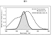
- FIG. 5 is a spectrum diagram showing an example of the fluorescence spectrum of the quantum dot 20R by a solid line and an example of an absorption spectrum of the phosphor 22R by a broken line.
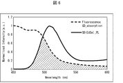
- FIG. 6 is a spectrum diagram showing an example of the fluorescence spectrum of the quantum dot 20G by a solid line and an example of an absorption spectrum of the phosphor 22G by a broken line.
- FIG. 7 is a spectrum diagram showing an example of the fluorescence spectrum of the quantum dot 20B by a solid line and an example of an absorption spectrum of the phosphor 22B by a broken line. Hatched portions in FIG. 5 to FIG. 7 indicate portions where the fluorescence spectra of the respective quantum dots and the absorption spectra of the respective phosphors overlap. Each spectrum in FIGS. 5 to 7 is normalized with the maximum intensity being 1.
- the quantum dots 20R are CdSe-ZnS quantum dots manufactured by Mesolight.
- the quantum dot 20G is a CdSe quantum dot manufactured by Sigma Aldrich.
- the quantum dots 20B are ZnSe-ZnS quantum dots manufactured by Sigma Aldrich.
- the light emitting device 2 according to the present embodiment emits fluorescence by the same light emitting mechanism as the light emitting device 2 according to the previous embodiment. For this reason, also in the present embodiment, as in the previous embodiment, the light emitting device 2 capable of efficiently obtaining fluorescence from the phosphor can be obtained.
- the light emitting layer 10 in the pixel region RP ⁇ GP may be provided with a phosphor that emits phosphorescence instead of the phosphor as a light emitter. Also in this case, energy transfer by the Forster mechanism occurs from the quantum dots in the pixel region RP ⁇ GP to the phosphor.
- a phosphor that emits red light and green light as phosphorescence is relatively easy to synthesize, and light emission can be efficiently obtained from excitons that are energy transferred from quantum dots.
- FIG. 8 is a block diagram showing a light emitting device manufacturing apparatus 30 according to each of the embodiments described above.
- the light emitting device manufacturing apparatus 30 may include a controller 32 and a film forming apparatus 34.
- the controller 32 may control the film forming apparatus 34.
- the film forming apparatus 34 may form each layer of the light emitting device 2.
- a light emitting device comprises a light emitting layer in which quantum dots and a light emitting material which is a phosphor or phosphor are dispersed, a first electrode under the light emitting layer, and a second electrode over the light emitting layer
- the emission spectrum of the quantum dot and the absorption spectrum of the light emitter overlap at least in part.
- the peak wavelength of the emission spectrum of the quantum dot is shorter than the peak wavelength of the emission spectrum of the light emitter.
- the peak wavelength of the emission spectrum of the quantum dot is included in the absorption spectrum of the light emitter.
- the peak wavelength of the absorption spectrum of the light emitter is included in the emission spectrum of the quantum dot.
- the concentration of the quantum dot in the light emitting layer is 10% by weight and 30% by weight.
- the concentration of the light emitter in the light emitting layer is 0.1 weight percent to 1 weight percent.
- the light emitting device further includes an edge cover having a plurality of openings and defining the light emitting layer in a plurality of pixel regions, and in each of the plurality of openings, the light emitting layer covers the opening and the upper end of the edge cover is The periphery of the light emitting layer is enclosed.
- the peak wavelength of the emission spectrum of at least a part of the quantum dots is included in the violet region or the ultraviolet region.
- the light emitting layer comprises a photosensitive material, and the quantum dots and the light emitter are dispersed in the photosensitive material.
- the apparatus for manufacturing a light emitting device includes: a light emitting layer in which a quantum dot; and a light emitter which is a phosphor or a phosphor in which at least a part of an absorption spectrum overlaps with a light emission spectrum of the quantum dot; A film forming apparatus is provided which forms a first electrode lower than the light emitting layer and a second electrode upper than the light emitting layer.
Landscapes
- Physics & Mathematics (AREA)
- Engineering & Computer Science (AREA)
- Optics & Photonics (AREA)
- Chemical & Material Sciences (AREA)
- Crystallography & Structural Chemistry (AREA)
- Inorganic Chemistry (AREA)
- Nanotechnology (AREA)
- Manufacturing & Machinery (AREA)
- General Physics & Mathematics (AREA)
- Theoretical Computer Science (AREA)
- Electroluminescent Light Sources (AREA)
Abstract
deep-blue領域において発光スペクトルのピークを有する蛍光材料に、容易にエネルギー遷移を発生させ、発光の効率を改善させた発光デバイスを提供することを目的として、量子ドット(20)と蛍光体または燐光体である発光体(22)とが分散する発光層(10)と、前記発光層(10)よりも下層の第1電極(4)と、前記発光層(10)よりも上層の第2電極(16)とを備え、前記量子ドット(20)の発光スペクトルと、前記発光体(22)の吸収スペクトルとが少なくとも一部において重なる発光デバイス(2)を提供する。
Description
本発明は、量子ドットを含む発光素子を備えた発光デバイスおよび当該発光デバイスの製造装置に関する。
特許文献1には、発光効率を高めるために、熱活性化遅延蛍光(TADF:Thermally activated delayed fluorescence)を発する材料と蛍光を発する材料とを混合した発光層を備えた発光素子が記載されている。
特許文献1の発光素子においては、TADF材料の三重項励起状態から逆項間交差により、TADF材料の一重項励起状態を作り出す。その後、フェルスター遷移によって、TADF材料の一重項励起状態を、蛍光材料の一重項励起状態に遷移させて、蛍光を発生させる。
TADF材料の三重項励起準位と一重項励起準位とのエネルギーギャップは非常に小さい。このため、特許文献1の発光素子においては、TADF材料の一重項励起状態から項間交差により、TADF材料の三重項励起状態が容易に作り出される。この状態においては、TADF材料の三重項励起状態から、蛍光材料の三重項励起状態へのデクスター遷移が発生しうる。蛍光材料の三重項励起状態から基底状態への失活過程は、非発光の過程である。このため、特許文献1の発光素子においては、発光効率が低下する可能性がある。
また、紫領域のような短波長の領域に発光スペクトルのピーク波長を有し、量子効率のよいTADF材料を合成することは困難である。このため、TADF材料から、deep-blue領域において発光スペクトルのピークを有する蛍光材料へエネルギーを遷移させることは困難である。
上記課題を解決するために、本発明の表示デバイスは、量子ドットと蛍光体または燐光体である発光体とが分散する発光層と、前記発光層よりも下層の第1電極と、前記発光層よりも上層の第2電極とを備えた発光デバイスであって、前記量子ドットの発光スペクトルと、前記発光体の吸収スペクトルとが少なくとも一部において重なる。
上記構成により、発光体の発光の効率を向上させることができる。また、deep-blue領域において発光スペクトルのピークを有する発光体に、エネルギー遷移を発生させることが、比較的容易となる。
本明細書において、発光デバイスの発光層から第1電極への方向を「下方向」、発光デバイスの発光層から第2電極への方向を「上方向」として記載する。
図1の(a)は、本実施形態に係る発光デバイス2の概略断面図である。
図1の(a)に示すように、発光デバイス2は、図示しないTFT(Thin Film Transistor)が形成されたアレイ基板3上に、各層が積層された構造を備える。アレイ基板3の上層に形成された第1電極4は、アレイ基板3のTFTと電気的に接続されている。発光デバイス2は、第1電極4上に、正孔注入層6と、正孔輸送層8と、発光層10と、電子輸送層12と、電子注入層14と、第2電極16とを、下層からこの順に備える。本実施形態においては、第1電極4はアノードであり、第2電極16はカソードである。
発光層10は、ホスト18と、量子ドット(半導体ナノ粒子)20と、発光体としての蛍光体22とを有する。量子ドット20および蛍光体22は、ホスト18中に分散する。
ホスト18は、正孔および電子の注入と輸送との機能を有する化合物を備える。ホスト18は、感光性材料を備えていてもよい。ホスト18は、図示しない分散材料をさらに備えていてもよい。
発光デバイス2において、第1電極4と第2電極16との間に電位差をかけることにより、第1電極4からは正孔が、第2電極16からは電子が、発光層10に向かって注入される。図1の(a)に示すように、第1電極4からの正孔は、正孔注入層6、および正孔輸送層8を介して、発光層10に到達する。第2電極16からの電子は、電子注入層14、および電子輸送層12を介して、発光層10に到達する。
発光層10に到達した正孔と電子とは、ホスト18を介して、量子ドット20において再結合し、励起子が生成される。このように、発光層10において励起子が生成されるように、正孔注入層6および正孔輸送層8の正孔輸送性、ならびに、電子注入層14および電子輸送層12の電子輸送性が調節される。
量子ドット20は、価電子帯準位と伝導帯準位とを有する。量子ドット20が、正孔と電子との再結合により生じた励起子からエネルギーを与えられると、量子ドット20の価電子帯準位から伝導帯準位に励起子が励起される。量子ドット20としては、例えば、コアにCdSe、シェルにZnSを備えた、コア/シェル構造を有する半導体ナノ粒子であってもよい。
蛍光体22は、基底準位、一重項励起準位、および三重項励起準位を有し、基底準位から一重項励起準位へと励起された励起子が、基底準位へと遷移する際に蛍光を発する蛍光材料である。
図1の(b)は、量子ドット20の蛍光スペクトルの例を実線にて、蛍光体22の吸収スペクトルの例を破線にて示すスペクトル図である。図1の(b)におけるハッチング箇所は、量子ドット20の蛍光スペクトルと、蛍光体22の吸収スペクトルとが、重なる部分を示す。本明細書におけるスペクトル図は何れも、横軸に波長、縦軸に規格化されたスペクトル強度を採る。図1の(b)におけるそれぞれのスペクトルは、最大強度を1として規格化されている。
図2は、本実施形態に係る発光デバイス2の発光機構を説明するための図である。図2の左右の分子軌道ダイヤグラムは、それぞれ、量子ドット20と蛍光体22との分子軌道を示すダイヤグラムである。なお、量子ドットの分子軌道ダイヤグラムにおいて、VBは価電子帯準位、CBは伝導帯準位を表す。また、蛍光体の分子軌道ダイヤグラムにおいて、S0は基底準位、S1は一重項励起準位を表し、三重項励起準位については、図示を省略している。なお、図2に示すように、本実施形態においては、量子ドット20の伝導帯準位は、蛍光体22の一重項励起準位よりも高い。このことは、量子ドット20の発光スペクトルのピーク波長が、蛍光体22の発光スペクトルのピーク波長よりも短いことに相当する。
図1および図2を参照して、本実施形態に係る発光デバイス2の発光機構を詳細に説明する。
図2に示すように、発光層10に到達した正孔と電子とが、ホスト18を介して、量子ドット20において再結合すると、正孔と電子との再結合によって、量子ドット20において、励起子が発生する。当該励起子は、量子ドット20の価電子帯準位から伝導帯準位に励起される。
ここで、量子ドット20の伝導帯準位の励起子は、フェルスター機構によるエネルギー移動によって、蛍光体22の一重項励起準位に遷移する。フェルスター機構は、本実施形態においては、量子ドット20と蛍光体22との間の双極子振動の共鳴現象を通じてエネルギー移動が起こる機構である。フェルスター機構によるエネルギー移動には、量子ドット20と蛍光体22との直接的な接触は必要ない。フェルスター機構の速度定数をkh*→gとすると、kh*→gは下記の数式(1)によって示される。

速度定数kh*→gが大きいほど、フェルスター機構によるエネルギー移動は優勢となる。このことから、量子ドット20から蛍光体22へのエネルギー移動は、量子ドット20の発光スペクトルと、蛍光体22の吸収スペクトルとの重なりがあることが求められる。
図1の(b)に示すように、本実施形態における量子ドット20の蛍光スペクトルと、蛍光体22の吸収スペクトルとは、少なくとも一部において重なっている。このため、互いの分子間距離が十分に近い量子ドット20と蛍光体22との間においては、上述のエネルギー移動が発生する。
また、図1の(b)に示すように、本実施形態においては、量子ドット20の発光スペクトルのピーク波長は、蛍光体22の吸収スペクトルに含まれている。また、蛍光体22の吸収スペクトルのピーク波長は、量子ドット20の発光スペクトルに含まれている。このため、上述のエネルギー移動がより優位に発生する。
最後に、蛍光体22の一重項励起準位から基底準位に、励起子が遷移する際に、一重項励起準位と基底準位とのエネルギー差に等しいエネルギーを有する蛍光が、蛍光体22から放射される。上記機構により、発光デバイス2から蛍光が得られる。
本実施形態における発光デバイス2においては、発生した励起子が、フェルスター機構のエネルギー移動によって、量子ドット20から蛍光体22へ移動し、蛍光体22において蛍光が生じる。量子ドット20から蛍光体22へのエネルギー移動において、非発光過程を発生させるデクスター遷移は発生しない。このため、本実施形態に係る発光デバイス2は、蛍光体22へのエネルギー移動する励起子からより効率的に蛍光を得ることが可能である。
また、熱活性化遅延蛍光体と比較して、紫領域または紫外領域の短波長の蛍光を発する量子ドットは合成が容易である。すなわち、deep-blue領域において発光スペクトルのピークを有する蛍光材料へ効率的にエネルギーを遷移させる量子ドットは、熱活性化遅延蛍光体と比較して合成しやすい。したがって、本実施形態に係る発光デバイス2は、従来よりも簡便に製造でき、効率的にdeep-blue領域の蛍光を得られる。ここで、紫領域または紫外領域の光とは、420nm以下の波長帯域に発光中心波長を有する光である。
量子ドット20の発光層10における濃度は、例えば、例えば、0.1質量パーセント~1質量パーセントである。量子ドット20の濃度が上記範囲内であれば、濃度消失により発光効率が落ちることを低減し、分散材料における励起子の発生を低減できる。
また、蛍光体22の発光層における濃度は、10質量パーセント~30質量パーセントである。蛍光体22の濃度が上記範囲内であれば、効率的に前述のエネルギー移動を発生させることが可能である。
なお、本実施形態において、発光層10は発光体として蛍光体22を備える。しかし、これに限られず、発光層10は、発光体として、蛍光体の代わりに、燐光を発する燐光体を備えていてもよい。この場合においても、量子ドットから燐光体へ、フェルスター機構によるエネルギー移動が発生する。その後、項間交差により、燐光体の一重項励起準位から三重項励起準位へ励起子が遷移する。燐光体の三重項励起準位から基底準位へ励起子が遷移する際に、燐光体から燐光を得ることができる。したがって、上記構成においても、より効率的にdeep-blue領域の燐光を得ることが可能である。
〔実施形態2〕
図3は、本実施形態に係る発光デバイス2の拡大上面図、および拡大断面図である。図3の(a)は、発光デバイス2の画素周辺の上面を、電子輸送層12、電子注入層14、および第2電極16を透過して示す図である。図3の(b)は、図3の(a)のA-A線矢視断面図である。
図3は、本実施形態に係る発光デバイス2の拡大上面図、および拡大断面図である。図3の(a)は、発光デバイス2の画素周辺の上面を、電子輸送層12、電子注入層14、および第2電極16を透過して示す図である。図3の(b)は、図3の(a)のA-A線矢視断面図である。
本実施形態においては、発光デバイス2は、前実施形態と比較して、複数の画素領域RP・GP・BPを備える。画素領域RPには、第1電極4上に、正孔注入層6R、正孔輸送層8R、および発光層10Rが、下方から順に形成されている。画素領域GP・BPにおいても同様に、正孔注入層6G・6B、正孔輸送層8G・8B、および発光層10G・10Bが、下方から順にそれぞれ形成されている。発光デバイス2は、さらにエッジカバー24を備える。エッジカバー24は複数の開口を有し、複数の画素領域RP・GP・BPをそれぞれ規定する。
図4は、本実施形態に係る発光デバイス2の、エッジカバー、および発光層の形成位置の関係について説明する図である。図4の(a)は、図5における画素領域RPについて拡大した側断面図である。図4の(b)は、画素領域RPにおいて、エッジカバーの開口、および発光層の形成位置を示す上面図である。
図4の(a)に示すように、エッジカバー24は、画素領域RPにおける開口26Rと、上端28Rとを有する。開口26Rは、上端28Rよりも小さく形成され、エッジカバー24の空孔は、開口26Rから上端28Rへと次第に大きくなるように形成されている。
このため、図4の(a)および(b)に示すように、正孔輸送層の下端8REは、エッジカバー24の開口26Rよりも大きい。すなわち、正孔輸送層8より上層の発光層10はエッジカバー24の開口26Rを覆う。また、エッジカバー24の上端28Rは、発光層10の上端10REよりも上方にある。すなわち、エッジカバー24の上端28Rが発光層10の周囲を囲う。
再び図3を参照すると、画素領域RPにおける発光層10は、ホスト18Rと、量子ドット20Rと、蛍光体22Rとを備える。同様に、発光層10は、画素領域GPにおいては、ホスト18Gと、量子ドット20Gと、蛍光体22Gとを備え、画素領域BPにおいては、ホスト18Bと、量子ドット20Bと、蛍光体22Bとを備える。
本実施形態においては、複数の画素領域RP・GP・BPのうち、一部の画素領域おける発光層10は、他の異なる画素領域における発光層10が有する蛍光体と、異なる蛍光体を有する。例えば、本実施形態においては、画素領域RPにおける発光層10は、赤色光を蛍光として発する蛍光体22Rを備える。同様に、画素領域GPにおける発光層10は、緑色光を蛍光として発する蛍光体22Gを備え、画素領域BPにおける発光層10は、青色光を蛍光として発する蛍光体22Bを備える。
ここで、青色光とは、400nm以上500nm以下の波長帯域に発光中心波長を有する光である。また、緑色光とは、500nm超600nm以下の波長帯域に発光中心波長を有する光のことである。また、赤色光とは、600nm超780nm以下の波長帯域に発光中心波長を有する光のことである。
また、複数の画素領域RP・GP・BPのうち、一部の画素領域おける発光層10は、他の異なる画素領域における発光層10が有するホストまたは量子ドットと、異なるホストまたは量子ドットを有していてもよい。しかし、本実施形態においては、各画素領域におけるホスト18R・G・Bおよび量子ドット20R・G・Bは、それぞれ同じ部材を採用してもよい。
図5は、量子ドット20Rの蛍光スペクトルの例を実線にて、蛍光体22Rの吸収スペクトルの例を破線にて示すスペクトル図である。図6は、量子ドット20Gの蛍光スペクトルの例を実線にて、蛍光体22Gの吸収スペクトルの例を破線にて示すスペクトル図である。図7は、量子ドット20Bの蛍光スペクトルの例を実線にて、蛍光体22Bの吸収スペクトルの例を破線にて示すスペクトル図である。図5から図7におけるハッチング箇所は、それぞれの量子ドットの蛍光スペクトルと、それぞれの蛍光体の吸収スペクトルとが、重なる部分を示す。図5~7におけるそれぞれのスペクトルは、最大強度を1として規格化されている。
本実施形態において、量子ドット20Rは、Mesolight社製のCdSe-ZnS量子ドットである。また、量子ドット20Gは、Sigma Aldrich社製のCdSe量子ドットである。また、量子ドット20Bは、Sigma Aldrich社製のZnSe-ZnS量子ドットである。
図5から図7に示すように、同じ画素領域に含まれる量子ドットおよび蛍光体においては、量子ドットの発光スペクトルと、蛍光体の吸収スペクトルとの少なくとも一部が重なる。このため、本実施形態に係る発光デバイス2は、前実施形態に係る発光デバイス2と同様の発光機構にて蛍光を発する。このため、本実施形態においても、前実施形態と同様に、蛍光体から効率的に蛍光を得られる発光デバイス2が得られる。
また、各画素領域における蛍光体からの蛍光の波長が異なるため、TFTの制御により、各画素領域における蛍光体からの発光を制御することにより、多色表示を行うことが可能である発光デバイス2を提供できる。
なお、本実施形態においても、画素領域RP・GPにおける発光層10は、発光体として、蛍光体の代わりに、燐光を発する燐光体を備えていてもよい。この場合においても、画素領域RP・GPにおける量子ドットから燐光体へ、フェルスター機構によるエネルギー移動が発生する。赤色光および緑色光を燐光として発する燐光体は、合成が比較的容易であり、量子ドットからエネルギー移動した励起子から、効率よく発光を得ることができる。
図8は、上述の各実施形態に係る発光デバイスの製造装置30を示すブロック図である。発光デバイスの製造装置30は、コントローラ32と、成膜装置34とを備えていてもよい。コントローラ32は、成膜装置34を制御してもよい。成膜装置34は、発光デバイス2の各層を成膜してもよい。
〔まとめ〕
様態1の発光デバイスは、量子ドットと蛍光体または燐光体である発光体とが分散する発光層と、前記発光層よりも下層の第1電極と、前記発光層よりも上層の第2電極とを備えた発光デバイスであって、前記量子ドットの発光スペクトルと、前記発光体の吸収スペクトルとが少なくとも一部において重なる。
様態1の発光デバイスは、量子ドットと蛍光体または燐光体である発光体とが分散する発光層と、前記発光層よりも下層の第1電極と、前記発光層よりも上層の第2電極とを備えた発光デバイスであって、前記量子ドットの発光スペクトルと、前記発光体の吸収スペクトルとが少なくとも一部において重なる。
様態2においては、前記量子ドットにおいて発生した励起子が、双極子振動の共鳴現象を通じて、前記発光体の励起準位に遷移し、前記発光体が発光する。
様態3においては、前記量子ドットの発光スペクトルのピーク波長が、前記発光体の発光スペクトルのピーク波長よりも短い。
様態4においては、前記量子ドットの発光スペクトルのピーク波長が、前記発光体の吸収スペクトルに含まれる。
様態5においては、前記発光体の吸収スペクトルのピーク波長が、前記量子ドットの発光スペクトルに含まれる。
様態6においては、前記量子ドットの前記発光層における濃度が、10質量パーセント30質量パーセントである。
様態7においては、前記発光体の前記発光層における濃度が、0.1質量パーセント~1質量パーセントである。
様態8においては、複数の開口を有し、前記発光層を複数の画素領域に規定するエッジカバーを備え、前記複数の開口のそれぞれにおいて、前記発光層は開口を覆い、前記エッジカバーの上端が前記発光層の周囲を囲う。
様態9においては、少なくとも一部の前記量子ドットの発光スペクトルのピーク波長が、紫領域または紫外領域に含まれる。
様態10においては、前記発光層が感光性材料を備え、前記量子ドットと前記発光体とが前記感光性材料中に分散する。
様態11の発光デバイスの製造装置は、量子ドットと、吸収スペクトルの少なくとも一部が、前記量子ドットの発光スペクトルと重なる蛍光体または燐光体である発光体とが分散する発光層と、前記発光層よりも下層の第1電極と、前記発光層よりも上層の第2電極とを形成する成膜装置を備える。
本発明は上述した各実施形態に限定されるものではなく、請求項に示した範囲で種々の変更が可能であり、異なる実施形態にそれぞれ開示された技術的手段を適宜組み合わせて得られる実施形態についても本発明の技術的範囲に含まれる。さらに、各実施形態にそれぞれ開示された技術的手段を組み合わせることにより、新しい技術的特徴を形成することができる。
2 発光デバイス
4 第1電極
10 発光層
16 第2電極
18 ホスト
20 量子ドット
22 蛍光体
4 第1電極
10 発光層
16 第2電極
18 ホスト
20 量子ドット
22 蛍光体
Claims (11)
- 量子ドットと蛍光体または燐光体である発光体とが分散する発光層と、前記発光層よりも下層の第1電極と、前記発光層よりも上層の第2電極とを備えた発光デバイスであって、
前記量子ドットの発光スペクトルと、前記発光体の吸収スペクトルとが少なくとも一部において重なる発光デバイス。 - 前記量子ドットにおいて発生した励起子が、双極子振動の共鳴現象を通じて、前記発光体の励起準位に遷移し、前記発光体が発光する請求項1に記載の発光デバイス。
- 前記量子ドットの発光スペクトルのピーク波長が、前記発光体の発光スペクトルのピーク波長よりも短い請求項1または2に記載の発光デバイス。
- 前記量子ドットの発光スペクトルのピーク波長が、前記発光体の吸収スペクトルに含まれる請求項1から3の何れか1項に記載の発光デバイス。
- 前記発光体の吸収スペクトルのピーク波長が、前記量子ドットの発光スペクトルに含まれる請求項1から4の何れか1項に記載の発光デバイス。
- 前記量子ドットの前記発光層における濃度が、10質量パーセントから30質量パーセントである請求項1から5の何れか1項に記載の発光デバイス。
- 前記発光体の前記発光層における濃度が、0.1質量パーセントから1質量パーセントである請求項1から6の何れか1項に記載の発光デバイス。
- 複数の開口を有し、前記発光層を複数の画素領域に規定するエッジカバーを備え、前記複数の開口のそれぞれにおいて、前記発光層は開口を覆い、前記エッジカバーの上端が前記発光層の周囲を囲う請求項1から7の何れか1項に記載の発光デバイス。
- 少なくとも一部の前記量子ドットの発光スペクトルのピーク波長が、紫領域または紫外領域に含まれる請求項1から8の何れか1項に記載の発光デバイス。
- 前記発光層は感光性材料を備え、前記量子ドットと前記発光体とが前記感光性材料中に分散する請求項1から9の何れか1項に記載の発光デバイス。
- 量子ドットと、吸収スペクトルの少なくとも一部が、前記量子ドットの発光スペクトルと重なる蛍光体または燐光体である発光体とが分散する発光層と、前記発光層よりも下層の第1電極と、前記発光層よりも上層の第2電極とを形成する成膜装置を備えた発光デバイスの製造装置。
Priority Applications (2)
| Application Number | Priority Date | Filing Date | Title |
|---|---|---|---|
| PCT/JP2017/031895 WO2019049191A1 (ja) | 2017-09-05 | 2017-09-05 | 発光デバイス、発光デバイスの製造装置 |
| US16/644,042 US20210135137A1 (en) | 2017-09-05 | 2017-09-05 | Light emitting device and manufacturing apparatus of light emitting device |
Applications Claiming Priority (1)
| Application Number | Priority Date | Filing Date | Title |
|---|---|---|---|
| PCT/JP2017/031895 WO2019049191A1 (ja) | 2017-09-05 | 2017-09-05 | 発光デバイス、発光デバイスの製造装置 |
Publications (1)
| Publication Number | Publication Date |
|---|---|
| WO2019049191A1 true WO2019049191A1 (ja) | 2019-03-14 |
Family
ID=65633688
Family Applications (1)
| Application Number | Title | Priority Date | Filing Date |
|---|---|---|---|
| PCT/JP2017/031895 Ceased WO2019049191A1 (ja) | 2017-09-05 | 2017-09-05 | 発光デバイス、発光デバイスの製造装置 |
Country Status (2)
| Country | Link |
|---|---|
| US (1) | US20210135137A1 (ja) |
| WO (1) | WO2019049191A1 (ja) |
Cited By (1)
| Publication number | Priority date | Publication date | Assignee | Title |
|---|---|---|---|---|
| WO2021053793A1 (ja) * | 2019-09-19 | 2021-03-25 | シャープ株式会社 | 発光デバイスおよび発光デバイスの製造方法 |
Citations (4)
| Publication number | Priority date | Publication date | Assignee | Title |
|---|---|---|---|---|
| JP2012186460A (ja) * | 2011-02-16 | 2012-09-27 | Semiconductor Energy Lab Co Ltd | 発光素子 |
| JP2013539584A (ja) * | 2010-07-26 | 2013-10-24 | メルク パテント ゲーエムベーハー | 量子ドットおよびホスト |
| JP2015220069A (ja) * | 2014-05-16 | 2015-12-07 | 株式会社ジャパンディスプレイ | 表示装置 |
| US20170186988A1 (en) * | 2015-12-24 | 2017-06-29 | Samsung Display Co., Ltd. | Light emitting diode and display device including the same |
-
2017
- 2017-09-05 US US16/644,042 patent/US20210135137A1/en not_active Abandoned
- 2017-09-05 WO PCT/JP2017/031895 patent/WO2019049191A1/ja not_active Ceased
Patent Citations (4)
| Publication number | Priority date | Publication date | Assignee | Title |
|---|---|---|---|---|
| JP2013539584A (ja) * | 2010-07-26 | 2013-10-24 | メルク パテント ゲーエムベーハー | 量子ドットおよびホスト |
| JP2012186460A (ja) * | 2011-02-16 | 2012-09-27 | Semiconductor Energy Lab Co Ltd | 発光素子 |
| JP2015220069A (ja) * | 2014-05-16 | 2015-12-07 | 株式会社ジャパンディスプレイ | 表示装置 |
| US20170186988A1 (en) * | 2015-12-24 | 2017-06-29 | Samsung Display Co., Ltd. | Light emitting diode and display device including the same |
Cited By (2)
| Publication number | Priority date | Publication date | Assignee | Title |
|---|---|---|---|---|
| WO2021053793A1 (ja) * | 2019-09-19 | 2021-03-25 | シャープ株式会社 | 発光デバイスおよび発光デバイスの製造方法 |
| US12356788B2 (en) | 2019-09-19 | 2025-07-08 | Sharp Kabushiki Kaisha | Light emitting device and method for manufacturing light emitting device |
Also Published As
| Publication number | Publication date |
|---|---|
| US20210135137A1 (en) | 2021-05-06 |
Similar Documents
| Publication | Publication Date | Title |
|---|---|---|
| US11271050B2 (en) | Color control encapsulation layer and display apparatus including the same | |
| JP5840372B2 (ja) | 高効率ハイブリッド発光ダイオード | |
| CN102024844B (zh) | 有机发光显示设备 | |
| WO2021044558A1 (ja) | 発光素子、発光デバイス、発光素子の製造方法 | |
| KR20170072728A (ko) | 유기발광 표시장치 | |
| CN102907176A (zh) | 发光元件、发光元件的制造方法以及显示装置 | |
| WO2019064541A1 (ja) | 発光装置および表示装置 | |
| US10121983B2 (en) | Light-emitting device including nano particle having core shell structure | |
| KR102282030B1 (ko) | 표시 장치 | |
| JP2016062899A (ja) | 半導体発光装置 | |
| CN108029163A (zh) | 有机电致发光装置、有机电致发光装置的制造方法、照明装置和显示装置 | |
| US11502266B2 (en) | Light emitting element comprising quantum dots and method for producing light emitting element | |
| JP5607733B2 (ja) | Oledベースの発光デバイス | |
| US11805663B2 (en) | Light emitting device and display device | |
| WO2019049191A1 (ja) | 発光デバイス、発光デバイスの製造装置 | |
| CN115428589A (zh) | 发光器件 | |
| WO2019049190A1 (ja) | 発光デバイス、発光デバイスの製造装置 | |
| JP6404636B2 (ja) | 表示装置 | |
| CN111052410B (zh) | 发光器件 | |
| TW202207487A (zh) | 全彩發光器件 | |
| CN112447917A (zh) | 有机发光元件 | |
| US20230337455A1 (en) | Light-emitting element, light-emitting device, method for manufacturing light-emitting element, and method for driving light-emitting element | |
| CN109360848B (zh) | 像素结构、显示基板及显示装置 | |
| WO2019186846A1 (ja) | 発光素子および表示装置 | |
| JPWO2012131793A1 (ja) | 発光素子 |
Legal Events
| Date | Code | Title | Description |
|---|---|---|---|
| 121 | Ep: the epo has been informed by wipo that ep was designated in this application |
Ref document number: 17924634 Country of ref document: EP Kind code of ref document: A1 |
|
| NENP | Non-entry into the national phase |
Ref country code: DE |
|
| 122 | Ep: pct application non-entry in european phase |
Ref document number: 17924634 Country of ref document: EP Kind code of ref document: A1 |
|
| NENP | Non-entry into the national phase |
Ref country code: JP |