JP6404636B2 - 表示装置 - Google Patents
表示装置 Download PDFInfo
- Publication number
- JP6404636B2 JP6404636B2 JP2014166620A JP2014166620A JP6404636B2 JP 6404636 B2 JP6404636 B2 JP 6404636B2 JP 2014166620 A JP2014166620 A JP 2014166620A JP 2014166620 A JP2014166620 A JP 2014166620A JP 6404636 B2 JP6404636 B2 JP 6404636B2
- Authority
- JP
- Japan
- Prior art keywords
- display device
- light emitting
- region
- light
- transmittance
- Prior art date
- Legal status (The legal status is an assumption and is not a legal conclusion. Google has not performed a legal analysis and makes no representation as to the accuracy of the status listed.)
- Active
Links
- 239000002096 quantum dot Substances 0.000 claims description 53
- 239000000758 substrate Substances 0.000 claims description 44
- 238000002834 transmittance Methods 0.000 claims description 31
- 229920005989 resin Polymers 0.000 claims description 30
- 239000011347 resin Substances 0.000 claims description 30
- 238000004519 manufacturing process Methods 0.000 claims description 16
- 239000003086 colorant Substances 0.000 claims description 9
- 230000001678 irradiating effect Effects 0.000 claims description 8
- 238000000034 method Methods 0.000 claims description 8
- 238000010894 electron beam technology Methods 0.000 claims description 4
- 230000004075 alteration Effects 0.000 claims description 3
- 239000010410 layer Substances 0.000 description 98
- 238000005401 electroluminescence Methods 0.000 description 21
- 239000010408 film Substances 0.000 description 18
- 239000000463 material Substances 0.000 description 16
- 239000011229 interlayer Substances 0.000 description 12
- 239000011159 matrix material Substances 0.000 description 10
- 238000007789 sealing Methods 0.000 description 7
- 230000000694 effects Effects 0.000 description 6
- 239000010419 fine particle Substances 0.000 description 5
- 239000004065 semiconductor Substances 0.000 description 5
- XLOMVQKBTHCTTD-UHFFFAOYSA-N Zinc monoxide Chemical compound [Zn]=O XLOMVQKBTHCTTD-UHFFFAOYSA-N 0.000 description 4
- 239000002245 particle Substances 0.000 description 4
- 229910052581 Si3N4 Inorganic materials 0.000 description 3
- VYPSYNLAJGMNEJ-UHFFFAOYSA-N Silicium dioxide Chemical compound O=[Si]=O VYPSYNLAJGMNEJ-UHFFFAOYSA-N 0.000 description 3
- 229910010272 inorganic material Inorganic materials 0.000 description 3
- 239000011147 inorganic material Substances 0.000 description 3
- 239000011368 organic material Substances 0.000 description 3
- HQVNEWCFYHHQES-UHFFFAOYSA-N silicon nitride Chemical compound N12[Si]34N5[Si]62N3[Si]51N64 HQVNEWCFYHHQES-UHFFFAOYSA-N 0.000 description 3
- 229910052814 silicon oxide Inorganic materials 0.000 description 3
- 239000004642 Polyimide Substances 0.000 description 2
- NIXOWILDQLNWCW-UHFFFAOYSA-N acrylic acid group Chemical group C(C=C)(=O)O NIXOWILDQLNWCW-UHFFFAOYSA-N 0.000 description 2
- 239000012790 adhesive layer Substances 0.000 description 2
- 238000000149 argon plasma sintering Methods 0.000 description 2
- 230000015572 biosynthetic process Effects 0.000 description 2
- 238000006243 chemical reaction Methods 0.000 description 2
- 150000001875 compounds Chemical class 0.000 description 2
- 230000005284 excitation Effects 0.000 description 2
- 238000000605 extraction Methods 0.000 description 2
- 238000002347 injection Methods 0.000 description 2
- 239000007924 injection Substances 0.000 description 2
- 229910052751 metal Inorganic materials 0.000 description 2
- 239000002184 metal Substances 0.000 description 2
- 239000000203 mixture Substances 0.000 description 2
- 230000003287 optical effect Effects 0.000 description 2
- 238000005192 partition Methods 0.000 description 2
- 229920001721 polyimide Polymers 0.000 description 2
- 239000000725 suspension Substances 0.000 description 2
- 239000010409 thin film Substances 0.000 description 2
- 239000011787 zinc oxide Substances 0.000 description 2
- 229910004613 CdTe Inorganic materials 0.000 description 1
- 239000004952 Polyamide Substances 0.000 description 1
- 239000000853 adhesive Substances 0.000 description 1
- 230000001070 adhesive effect Effects 0.000 description 1
- 230000002776 aggregation Effects 0.000 description 1
- 238000004220 aggregation Methods 0.000 description 1
- UHYPYGJEEGLRJD-UHFFFAOYSA-N cadmium(2+);selenium(2-) Chemical compound [Se-2].[Cd+2] UHYPYGJEEGLRJD-UHFFFAOYSA-N 0.000 description 1
- 230000008859 change Effects 0.000 description 1
- 238000005520 cutting process Methods 0.000 description 1
- 230000006866 deterioration Effects 0.000 description 1
- 230000005684 electric field Effects 0.000 description 1
- 230000005525 hole transport Effects 0.000 description 1
- 230000006872 improvement Effects 0.000 description 1
- 230000002779 inactivation Effects 0.000 description 1
- AMGQUBHHOARCQH-UHFFFAOYSA-N indium;oxotin Chemical compound [In].[Sn]=O AMGQUBHHOARCQH-UHFFFAOYSA-N 0.000 description 1
- 239000002346 layers by function Substances 0.000 description 1
- 150000002894 organic compounds Chemical class 0.000 description 1
- TWNQGVIAIRXVLR-UHFFFAOYSA-N oxo(oxoalumanyloxy)alumane Chemical compound O=[Al]O[Al]=O TWNQGVIAIRXVLR-UHFFFAOYSA-N 0.000 description 1
- 229920002647 polyamide Polymers 0.000 description 1
- 230000001681 protective effect Effects 0.000 description 1
- 230000003595 spectral effect Effects 0.000 description 1
- 238000011282 treatment Methods 0.000 description 1
Images


Landscapes
- Optical Filters (AREA)
- Electroluminescent Light Sources (AREA)
- Devices For Indicating Variable Information By Combining Individual Elements (AREA)
Description
限定するものではない。また、本明細書と各図において、既出の図に関して前述したものと同様の要素には、同一の符号を付して、詳細な説明を省略することがある。
<表示装置の構造>
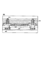
図1に、本発明の一実施形態に係る表示装置100の概略構成を示す。本実施形態に示す表示装置100は、発光素子の発光層として有機EL材料を用いた有機EL表示装置である。表示装置100は、基板101上に形成された、画素部(表示領域)102、走査線駆動回路103、データ線駆動回路104、及びドライバIC105を備えている。さらに、走査線駆動回路103及びデータ線駆動回路104に信号を与えるためのFPC(Flexible Printed Circuits)を備えていてもよい。
図4に、本実施形態の表示装置100の製造工程を示す。図4(A)において、基板301上に公知の技術によりTFT303を形成した後、第1層間絶縁層304、第2層間絶縁層305を形成し、陽極として機能する画素電極306を形成する。さらに、画素電極306を形成した後、ポリイミドやアクリル等の樹脂材料を成膜し、パターニングを行ってバンク308を形成する。バンク308は、各画素を区画する隔壁として機能し、バンク308を形成していない部分が各画素の表示領域を構成することとなる。なお、TFT303の上方にバンク308を設けることにより、各画素の表示領域をできるだけ広く確保することが好ましい。
本発明の第2の実施形態に係る表示装置の構成について説明する。本実施の形態に係る表示装置は、図3に示す発光層310として、有機EL材料に代えて、量子ドットを含む樹脂材料を用いる。量子ドットについては、第1の実施形態で説明した量子ドットを用いれば良い。
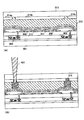
本発明の第3の実施形態に係る表示装置の構成について説明する。図6に、本実施形態に係る表示装置600における画素部の断面図を示す。図6において、図3と異なる点は、光遮蔽領域315の下方において発光層310に対してもエネルギー線の照射を行い、発光層を不活性化した不活性領域601を形成した点である。
102 画素部
103 走査線駆動回路
104 データ線駆動回路
105 ドライバIC
201 画素
201a Rに対応する画素
201b Gに対応する画素
201c Bに対応する画素
202 TFT
203 バンク
301 TFT基板
302 下地層
303 TFT
304 第1層間絶縁層
305 第2層間絶縁層
306 画素電極
307 発光素子
308 バンク
309 共通電極
310 発光層
311 封止膜
312 充填層
313 基板
314a Rに対応するカラーフィルタ
314b Gに対応するカラーフィルタ
314c Bに対応するカラーフィルタ
315 光遮蔽領域
401 エネルギー線
501a Rに対応する画素
501b Gに対応する画素
501c Bに対応する画素
601 不活性領域
Claims (17)
- 複数の発光素子が設けられた第1基板と、
前記発光素子の前記第1基板とは反対の側に、複数の発光素子にまたがって位置し、量子ドットを含む樹脂層と、
を備え、
前記発光素子と重なる領域に位置する前記樹脂層は、第1透過率を有し、
前記複数の発光素子の境界の少なくとも一部に位置する前記樹脂層は、前記第1透過率よりも透過率が低い第2透過率を有する表示装置。 - 前記量子ドットは、前記樹脂層に分散されていることを特徴とする請求項1に記載の表示装置。
- 前記複数の発光素子の境界の、前記少なくとも一部とは異なる他の一部に位置する前記樹脂層は、前記第1透過率よりも透過率が低く、且つ前記第2透過率とは異なる第3透過率を有することを特徴とする請求項1に記載の表示装置。
- 前記樹脂層の前記第2透過率を有する領域は、互いに隣接し、且つ異なる色の光を発する前記発光素子の境界に位置することを特徴とする請求項1に記載の表示装置。
- 前記樹脂層は、前記第1透過率を有する領域と前記第2透過率を有する領域との両方に、前記量子ドットが分散していることを特徴とする請求項1に記載の表示装置。
- 前記第1透過率を有する領域における前記量子ドットの密度と、前記第2透過率を有する領域における前記量子ドットの密度とが、同じであることを特徴とする請求項5に記載の表示装置。
- 複数のカラーフィルタが設けられた第2基板を有し、
前記複数のカラーフィルタは、互いに隙間を介して離間しており、
前記樹脂層の前記第2透過率を有する領域は、前記隙間に対向することを特徴とする請求項1に記載の表示装置。 - 前記第2透過率を有する領域の一部は、前記隙間に位置することを特徴とする請求項7に記載の表示装置。
- 前記複数の発光素子の各々は、発光層を有し、
前記発光層の少なくとも一部は、前記複数の発光素子にまたがって位置し、且つ前記樹脂層の前記第2透過率を有する領域と対向する対向領域を有し、
前記対向領域は、前記発光層の前記少なくとも一部の、前記対向領域とは異なる領域よりも、抵抗が高いことを特徴とする請求項1から請求項8のいずれか1項に記載の表示装置。 - 複数の発光素子が設けられた第1基板と、複数のカラーフィルタが設けられた第2基板とを、量子ドットが分散する樹脂層を介して貼り合わせる工程と、
前記樹脂層の一部にエネルギー線を照射して、該樹脂層の変質により他の部分に比べて透過率の低くなった領域を形成する工程と、
を備えたことを特徴とする表示装置の製造方法。 - 前記樹脂層の前記一部は、互いに異なる色の光を発する発光素子の境界に位置することを特徴とする請求項10に記載の表示装置の製造方法。
- 前記複数のカラーフィルタは、互いに隙間を介して離間しており、
前記樹脂層の前記一部は、前記隙間に対向することを特徴とする請求項10又は請求項11に記載の表示装置の製造方法。 - 前記エネルギー線の照射は、前記エネルギー線を走査することにより行われることを特徴とする請求項10から請求項12のいずれか1項に記載の表示装置の製造方法。
- 前記エネルギー線の照射は、マスクを用いて前記エネルギー線を一括照射することにより行われることを特徴とする請求項10から請求項12のいずれか1項に記載の表示装置の製造方法。
- 前記エネルギー線の照射は、前記第2基板を介して行われることを特徴とする請求項10から請求項14のいずれか1項に記載の表示装置の製造方法。
- 前記エネルギー線は、レーザ光、紫外光、電子線及び赤外光から選択された少なくとも1つであることを特徴とする請求項10から請求項15のいずれか1項に記載の表示装置の製造方法。
- 前記複数の発光素子の各々は、発光層を有し、
前記発光層の少なくとも一部は、前記複数の発光素子にまたがって位置し、且つ前記樹脂層の前記一部と対向する領域を有し、
前記エネルギー線の照射により、前記樹脂層の前記一部と対向する前記領域を高抵抗化することを特徴とする請求項10から請求項16のいずれか1項に記載の表示装置の製造方法。
Priority Applications (1)
| Application Number | Priority Date | Filing Date | Title |
|---|---|---|---|
| JP2014166620A JP6404636B2 (ja) | 2014-08-19 | 2014-08-19 | 表示装置 |
Applications Claiming Priority (1)
| Application Number | Priority Date | Filing Date | Title |
|---|---|---|---|
| JP2014166620A JP6404636B2 (ja) | 2014-08-19 | 2014-08-19 | 表示装置 |
Publications (3)
| Publication Number | Publication Date |
|---|---|
| JP2016042450A JP2016042450A (ja) | 2016-03-31 |
| JP2016042450A5 JP2016042450A5 (ja) | 2017-09-07 |
| JP6404636B2 true JP6404636B2 (ja) | 2018-10-10 |
Family
ID=55592109
Family Applications (1)
| Application Number | Title | Priority Date | Filing Date |
|---|---|---|---|
| JP2014166620A Active JP6404636B2 (ja) | 2014-08-19 | 2014-08-19 | 表示装置 |
Country Status (1)
| Country | Link |
|---|---|
| JP (1) | JP6404636B2 (ja) |
Families Citing this family (3)
| Publication number | Priority date | Publication date | Assignee | Title |
|---|---|---|---|---|
| WO2023013011A1 (ja) * | 2021-08-06 | 2023-02-09 | シャープ株式会社 | 表示装置、および表示装置の製造方法 |
| WO2023013012A1 (ja) * | 2021-08-06 | 2023-02-09 | シャープ株式会社 | 電子デバイス、電子デバイスの製造方法 |
| JPWO2023013013A1 (ja) * | 2021-08-06 | 2023-02-09 |
Family Cites Families (7)
| Publication number | Priority date | Publication date | Assignee | Title |
|---|---|---|---|---|
| JP2007225858A (ja) * | 2006-02-23 | 2007-09-06 | Seiko Epson Corp | カラーフィルタ基板の製造方法、エレクトロルミネッセンス基板の製造方法、カラーフィルタ基板、エレクトロルミネッセンス基板、電気光学装置及び電子機器 |
| US7932972B2 (en) * | 2006-10-02 | 2011-04-26 | Lg Display Co., Ltd. | Substrate for liquid crystal display device and method of fabricating the same |
| JP4752814B2 (ja) * | 2007-06-21 | 2011-08-17 | パナソニック株式会社 | 有機デバイスおよびその製造方法 |
| JP2009087752A (ja) * | 2007-09-28 | 2009-04-23 | Dainippon Printing Co Ltd | 発光表示素子及び発光表示パネル |
| KR100951044B1 (ko) * | 2007-10-17 | 2010-04-05 | 삼성코닝정밀유리 주식회사 | 디스플레이 장치용 외광 차폐 필름의 제조 방법 |
| JP5193957B2 (ja) * | 2009-06-16 | 2013-05-08 | ローム株式会社 | 有機el素子及びその製造方法 |
| TW201427893A (zh) * | 2013-01-07 | 2014-07-16 | 群康科技(深圳)有限公司 | 圖案化色轉換膜及應用其之顯示裝置 |
-
2014
- 2014-08-19 JP JP2014166620A patent/JP6404636B2/ja active Active
Also Published As
| Publication number | Publication date |
|---|---|
| JP2016042450A (ja) | 2016-03-31 |
Similar Documents
| Publication | Publication Date | Title |
|---|---|---|
| US20180269260A1 (en) | Quantum dot array on directly patterned amoled displays and method of fabrication | |
| JP6131434B2 (ja) | 色転換層、色転換層を有する有機el発光表示パネル及び液晶表示パネル | |
| KR102370715B1 (ko) | 양자점을 포함하는 유기발광 다이오드 표시장치 | |
| US10978676B2 (en) | Organic light-emitting display device | |
| KR101731164B1 (ko) | 표시 장치 | |
| US10797115B2 (en) | Display panel and display apparatus using the same | |
| JP6487173B2 (ja) | 表示装置及びその製造方法 | |
| KR102119680B1 (ko) | 표시 장치 및 이의 구동 방법 | |
| TWI537645B (zh) | 顯示裝置 | |
| WO2016140130A1 (ja) | エレクトロルミネッセンス装置、及び製造方法 | |
| JP6558880B2 (ja) | 有機el表示装置の製造方法 | |
| EP2485567B1 (en) | Organic electroluminescence display apparatus | |
| JP2016042449A (ja) | 表示装置 | |
| JP2016048602A (ja) | 表示装置 | |
| JP2017091946A (ja) | 表示装置および表示装置の製造方法 | |
| JP6521610B2 (ja) | 画像表示装置 | |
| KR101736646B1 (ko) | 표시장치, 표시장치의 제조 방법 및 전자기기 | |
| US9362342B2 (en) | Light-emitting element display device | |
| JP6749160B2 (ja) | 表示装置 | |
| JP2017147059A (ja) | 電気光学装置及び電子機器 | |
| KR20160026015A (ko) | 디스플레이 패널 및 이의 제조 방법 | |
| US8872415B2 (en) | Substrate, display panel, and display apparatus | |
| KR20220137580A (ko) | 유기발광 표시장치 | |
| JP6404636B2 (ja) | 表示装置 | |
| US20150090987A1 (en) | Organic el display device |
Legal Events
| Date | Code | Title | Description |
|---|---|---|---|
| A521 | Request for written amendment filed |
Free format text: JAPANESE INTERMEDIATE CODE: A523 Effective date: 20170728 |
|
| A621 | Written request for application examination |
Free format text: JAPANESE INTERMEDIATE CODE: A621 Effective date: 20170728 |
|
| A977 | Report on retrieval |
Free format text: JAPANESE INTERMEDIATE CODE: A971007 Effective date: 20180629 |
|
| TRDD | Decision of grant or rejection written | ||
| A01 | Written decision to grant a patent or to grant a registration (utility model) |
Free format text: JAPANESE INTERMEDIATE CODE: A01 Effective date: 20180821 |
|
| A61 | First payment of annual fees (during grant procedure) |
Free format text: JAPANESE INTERMEDIATE CODE: A61 Effective date: 20180913 |
|
| R150 | Certificate of patent or registration of utility model |
Ref document number: 6404636 Country of ref document: JP Free format text: JAPANESE INTERMEDIATE CODE: R150 |
|
| R250 | Receipt of annual fees |
Free format text: JAPANESE INTERMEDIATE CODE: R250 |
|
| R250 | Receipt of annual fees |
Free format text: JAPANESE INTERMEDIATE CODE: R250 |
|
| R250 | Receipt of annual fees |
Free format text: JAPANESE INTERMEDIATE CODE: R250 |