JP6404636B2 - Display device - Google Patents
Display device Download PDFInfo
- Publication number
- JP6404636B2 JP6404636B2 JP2014166620A JP2014166620A JP6404636B2 JP 6404636 B2 JP6404636 B2 JP 6404636B2 JP 2014166620 A JP2014166620 A JP 2014166620A JP 2014166620 A JP2014166620 A JP 2014166620A JP 6404636 B2 JP6404636 B2 JP 6404636B2
- Authority
- JP
- Japan
- Prior art keywords
- display device
- light emitting
- region
- light
- transmittance
- Prior art date
- Legal status (The legal status is an assumption and is not a legal conclusion. Google has not performed a legal analysis and makes no representation as to the accuracy of the status listed.)
- Active
Links
- 239000002096 quantum dot Substances 0.000 claims description 53
- 239000000758 substrate Substances 0.000 claims description 44
- 238000002834 transmittance Methods 0.000 claims description 31
- 229920005989 resin Polymers 0.000 claims description 30
- 239000011347 resin Substances 0.000 claims description 30
- 238000004519 manufacturing process Methods 0.000 claims description 16
- 239000003086 colorant Substances 0.000 claims description 9
- 230000001678 irradiating effect Effects 0.000 claims description 8
- 238000000034 method Methods 0.000 claims description 8
- 238000010894 electron beam technology Methods 0.000 claims description 4
- 230000004075 alteration Effects 0.000 claims description 3
- 239000010410 layer Substances 0.000 description 98
- 238000005401 electroluminescence Methods 0.000 description 21
- 239000010408 film Substances 0.000 description 18
- 239000000463 material Substances 0.000 description 16
- 239000011229 interlayer Substances 0.000 description 12
- 239000011159 matrix material Substances 0.000 description 10
- 238000007789 sealing Methods 0.000 description 7
- 230000000694 effects Effects 0.000 description 6
- 239000010419 fine particle Substances 0.000 description 5
- 239000004065 semiconductor Substances 0.000 description 5
- XLOMVQKBTHCTTD-UHFFFAOYSA-N Zinc monoxide Chemical compound [Zn]=O XLOMVQKBTHCTTD-UHFFFAOYSA-N 0.000 description 4
- 239000002245 particle Substances 0.000 description 4
- 229910052581 Si3N4 Inorganic materials 0.000 description 3
- VYPSYNLAJGMNEJ-UHFFFAOYSA-N Silicium dioxide Chemical compound O=[Si]=O VYPSYNLAJGMNEJ-UHFFFAOYSA-N 0.000 description 3
- 229910010272 inorganic material Inorganic materials 0.000 description 3
- 239000011147 inorganic material Substances 0.000 description 3
- 239000011368 organic material Substances 0.000 description 3
- HQVNEWCFYHHQES-UHFFFAOYSA-N silicon nitride Chemical compound N12[Si]34N5[Si]62N3[Si]51N64 HQVNEWCFYHHQES-UHFFFAOYSA-N 0.000 description 3
- 229910052814 silicon oxide Inorganic materials 0.000 description 3
- 239000004642 Polyimide Substances 0.000 description 2
- NIXOWILDQLNWCW-UHFFFAOYSA-N acrylic acid group Chemical group C(C=C)(=O)O NIXOWILDQLNWCW-UHFFFAOYSA-N 0.000 description 2
- 239000012790 adhesive layer Substances 0.000 description 2
- 238000000149 argon plasma sintering Methods 0.000 description 2
- 230000015572 biosynthetic process Effects 0.000 description 2
- 238000006243 chemical reaction Methods 0.000 description 2
- 150000001875 compounds Chemical class 0.000 description 2
- 230000005284 excitation Effects 0.000 description 2
- 238000000605 extraction Methods 0.000 description 2
- 238000002347 injection Methods 0.000 description 2
- 239000007924 injection Substances 0.000 description 2
- 229910052751 metal Inorganic materials 0.000 description 2
- 239000002184 metal Substances 0.000 description 2
- 239000000203 mixture Substances 0.000 description 2
- 230000003287 optical effect Effects 0.000 description 2
- 238000005192 partition Methods 0.000 description 2
- 229920001721 polyimide Polymers 0.000 description 2
- 239000000725 suspension Substances 0.000 description 2
- 239000010409 thin film Substances 0.000 description 2
- 239000011787 zinc oxide Substances 0.000 description 2
- 229910004613 CdTe Inorganic materials 0.000 description 1
- 239000004952 Polyamide Substances 0.000 description 1
- 239000000853 adhesive Substances 0.000 description 1
- 230000001070 adhesive effect Effects 0.000 description 1
- 230000002776 aggregation Effects 0.000 description 1
- 238000004220 aggregation Methods 0.000 description 1
- UHYPYGJEEGLRJD-UHFFFAOYSA-N cadmium(2+);selenium(2-) Chemical compound [Se-2].[Cd+2] UHYPYGJEEGLRJD-UHFFFAOYSA-N 0.000 description 1
- 230000008859 change Effects 0.000 description 1
- 238000005520 cutting process Methods 0.000 description 1
- 230000006866 deterioration Effects 0.000 description 1
- 230000005684 electric field Effects 0.000 description 1
- 230000005525 hole transport Effects 0.000 description 1
- 230000006872 improvement Effects 0.000 description 1
- 230000002779 inactivation Effects 0.000 description 1
- AMGQUBHHOARCQH-UHFFFAOYSA-N indium;oxotin Chemical compound [In].[Sn]=O AMGQUBHHOARCQH-UHFFFAOYSA-N 0.000 description 1
- 239000002346 layers by function Substances 0.000 description 1
- 150000002894 organic compounds Chemical class 0.000 description 1
- TWNQGVIAIRXVLR-UHFFFAOYSA-N oxo(oxoalumanyloxy)alumane Chemical compound O=[Al]O[Al]=O TWNQGVIAIRXVLR-UHFFFAOYSA-N 0.000 description 1
- 229920002647 polyamide Polymers 0.000 description 1
- 230000001681 protective effect Effects 0.000 description 1
- 230000003595 spectral effect Effects 0.000 description 1
- 238000011282 treatment Methods 0.000 description 1
Images


Description
本発明は、エレクトロルミネセンス素子等の発光素子で構成される画素を有する表示装置に関する。特に、発光素子として、量子ドットを有する発光層を用いた表示装置に関する。 The present invention relates to a display device having a pixel including a light emitting element such as an electroluminescence element. In particular, the present invention relates to a display device using a light emitting layer having quantum dots as a light emitting element.
エレクトロルミネセンス(Electroluminescence:EL)現象を利用した発光素子として、エレクトロルミネセンス(以下「EL」ともいう)素子が知られている。EL素子は、発光層を構成する材料の選択により様々な波長の色で発光させることが可能であり、表示装置や照明器具への応用が進められている。 As a light-emitting element utilizing an electroluminescence (EL) phenomenon, an electroluminescence (hereinafter also referred to as “EL”) element is known. EL elements can emit light with various wavelengths depending on the selection of materials constituting the light-emitting layer, and their application to display devices and lighting fixtures is being promoted.
EL素子を表示装置に応用したEL表示装置においては、マトリクス状に配置した各画素に、発光素子としてのEL素子と、そのEL素子の発光制御を行うスイッチング素子とが設けられている。そして、画素ごとにスイッチング素子のオン/オフ制御することにより、全体として任意の画像を表示することが可能である。 In an EL display device in which an EL element is applied to a display device, each pixel arranged in a matrix is provided with an EL element as a light emitting element and a switching element for controlling light emission of the EL element. An arbitrary image can be displayed as a whole by controlling on / off of the switching element for each pixel.
近年、EL表示装置に用いられる発光素子として、量子ドット(Quantum dot:QD)を利用したものが各種提案されている。量子ドットは、nmオーダの半導体微粒子であって、外部からのエネルギーで発光を制御することの可能な発光材料であるとともに、外部からの電界で自ら発光させることも可能な発光材料である。従来の表示装置には、例えば、量子ドットを有する無機発光層を用いたもの(特許文献1)や、発光素子の光取り出し側に量子ドットを含む光散乱層を備えたもの(特許文献2)等が提案されている。 In recent years, various types of light-emitting elements that use quantum dots (QDs) have been proposed as light-emitting elements used in EL display devices. The quantum dot is a semiconductor fine particle of the order of nm, and is a light emitting material capable of controlling light emission with external energy and also capable of emitting light by an external electric field. Conventional display devices include, for example, a device using an inorganic light emitting layer having quantum dots (Patent Document 1), or a light scattering layer including quantum dots on the light extraction side of a light emitting element (Patent Document 2). Etc. have been proposed.
しかし、上述した従来の表示装置は、量子ドットを含有する発光層や光散乱層を、光の取り出し方向である縦方向に重ねたスタック構造とするものが多く、微細な画素を有する高精細の小型表示パネルに適用すると、隣接画素に光が漏れるといった問題が生じる虞があった。特に、画素ごとにR(赤)、G(緑)、B(青)に発光する発光素子を設けたEL表示装置においては、隣接画素への光漏れにより混色が発生し、正確な画像表示が出来ない虞があった。 However, many of the conventional display devices described above have a stack structure in which light-emitting layers and light-scattering layers containing quantum dots are stacked in the vertical direction, which is the light extraction direction. When applied to a small display panel, there is a risk that light may leak to adjacent pixels. In particular, in an EL display device provided with light emitting elements that emit R (red), G (green), and B (blue) for each pixel, color mixture occurs due to light leakage to adjacent pixels, and accurate image display is possible. There was a possibility that it could not be done.
そこで、本発明は、隣接画素への光漏れを防止して画素間の混色を防ぐことにより、画質の改善された表示装置を提供することを目的の一つとする。 Therefore, an object of the present invention is to provide a display device with improved image quality by preventing light leakage to adjacent pixels and preventing color mixture between pixels.
また、そのような表示装置を、製造工程を大幅に変更することなく、簡素な構成で実現することを目的の一つとする。 Another object is to realize such a display device with a simple configuration without significantly changing the manufacturing process.
本発明の一態様は、発光素子が設けられた第1基板と、複数のカラーフィルタが設けられた第2基板と、前記第1基板及び前記第2基板の間に設けられ、量子ドットを含み、且つ、透過率の異なる領域を含む充填層と、を備えた表示装置である。 One embodiment of the present invention includes a first substrate provided with a light-emitting element, a second substrate provided with a plurality of color filters, a quantum dot provided between the first substrate and the second substrate. And a filling layer including regions having different transmittances.
前記量子ドットは、前記充填層に分散されていてもよい。 The quantum dots may be dispersed in the packed layer.
前記充填層における前記透過率の異なる領域は、前記充填層が変質した領域であってもよい。 The region having a different transmittance in the packed layer may be a region in which the packed layer has been altered.
前記充填層の一部は、互いに異なる色の光を発する画素の境界に位置していてもよい。 A part of the filling layer may be located at a boundary between pixels emitting light of different colors.
前記複数のカラーフィルタは、マトリクス状に配置され、前記充填層の一部は、前記マトリクス状に配置された各カラーフィルタの隙間に位置していてもよい。 The plurality of color filters may be arranged in a matrix, and a part of the filling layer may be located in a gap between the color filters arranged in the matrix.
本発明の一態様は、発光素子が設けられた第1基板と、複数のカラーフィルタが設けられた第2基板とを、量子ドットが分散する充填層を介して貼り合わせる工程と、前記充填層の一部にエネルギー線を照射して、該充填層の変質により他の部分に比べて透過率の低くなった領域を形成する工程と、を備えた表示装置の製造方法である。 One embodiment of the present invention includes a step of bonding a first substrate provided with a light-emitting element and a second substrate provided with a plurality of color filters through a filling layer in which quantum dots are dispersed; And a step of irradiating a part of the substrate with energy rays to form a region having a lower transmittance than that of the other part due to the alteration of the filling layer.
前記充填層の一部は、互いに異なる色の光を発する画素の境界に位置していてもよい。 A part of the filling layer may be located at a boundary between pixels emitting light of different colors.
前記複数のカラーフィルタは、マトリクス状に配置され、前記充填層の一部は、前記マトリクス状に配置された各カラーフィルタの隙間に位置していてもよい。 The plurality of color filters may be arranged in a matrix, and a part of the filling layer may be located in a gap between the color filters arranged in the matrix.
前記エネルギー線の照射は、前記エネルギー線を走査して行ってもよいし、マスクを用いて前記エネルギー線を一括照射して行ってもよい。 The energy beam irradiation may be performed by scanning the energy beam, or may be performed by collectively irradiating the energy beam using a mask.
前記エネルギー線の照射は、前記対向基板を介して行ってもよい。 The irradiation with the energy beam may be performed through the counter substrate.
前記エネルギー線は、レーザ光、紫外光、電子線及び赤外光から選択された少なくとも1つであればよい。 The energy beam may be at least one selected from laser light, ultraviolet light, electron beam, and infrared light.
前記エネルギー線の照射により、前記他の部分に比べて透過率の低くなった領域の下方に位置する活性層を不活性化してもよい。 The active layer located below the region where the transmittance is lower than that of the other part may be deactivated by the irradiation of the energy beam.
以下、本発明の各実施の形態について、図面等を参照しつつ説明する。但し、本発明は、その要旨を逸脱しない範囲において様々な態様で実施することができ、以下に例示する実施の形態の記載内容に限定して解釈されるものではない。また、図面は、説明をより明確にするため、実際の態様に比べ、各部の幅、厚さ、形状等について模式的に表される場合があるが、あくまで一例であって、本発明の解釈を
限定するものではない。また、本明細書と各図において、既出の図に関して前述したものと同様の要素には、同一の符号を付して、詳細な説明を省略することがある。
Hereinafter, embodiments of the present invention will be described with reference to the drawings. However, the present invention can be implemented in various modes without departing from the gist thereof, and is not construed as being limited to the description of the embodiments exemplified below. Further, in order to make the explanation clearer, the drawings may be schematically represented with respect to the width, thickness, shape, and the like of each part as compared with the actual embodiment, but are merely examples, and the interpretation of the present invention. It is not intended to limit. In the present specification and drawings, the same elements as those described above with reference to the previous drawings may be denoted by the same reference numerals, and detailed description thereof may be omitted.
また、以下に示す実施形態では、基板上にスイッチング素子(例えば薄膜トランジスタ)及び発光素子が設けられたアクティブマトリクス型の表示装置を例示するが、本発明はこれに限定されるものではなく、基板上に発光素子のみが設けられた単純マトリクス型の表示装置にも適用できる。 In the embodiment described below, an active matrix display device in which a switching element (for example, a thin film transistor) and a light emitting element are provided over a substrate is illustrated, but the present invention is not limited to this, and the substrate is not limited thereto. The present invention can also be applied to a simple matrix display device in which only a light emitting element is provided.
(第1の実施形態)
<表示装置の構造>
図1に、本発明の一実施形態に係る表示装置100の概略構成を示す。本実施形態に示す表示装置100は、発光素子の発光層として有機EL材料を用いた有機EL表示装置である。表示装置100は、基板101上に形成された、画素部(表示領域)102、走査線駆動回路103、データ線駆動回路104、及びドライバIC105を備えている。さらに、走査線駆動回路103及びデータ線駆動回路104に信号を与えるためのFPC(Flexible Printed Circuits)を備えていてもよい。
(First embodiment)
<Structure of display device>
FIG. 1 shows a schematic configuration of a
図1に示す画素部102には、複数の画素がマトリクス状に配置される。各画素には、データ線駆動回路104から画像データに応じた信号が与えられ、該信号を各画素に設けられたスイッチング素子を介して画素電極に与えることにより画像データに応じた画面表示を行うことができる。スイッチング素子としては、TFT(薄膜トランジスタ)等の三端子素子やMIM等の二端子素子を用いることができる。
A plurality of pixels are arranged in a matrix in the
図2に、図1に示す表示装置100における画素部102の概略構成を示す。本実施形態において、画素201は、赤(R)に対応するサブ画素201a、緑(G)に対応するサブ画素201b及び青(B)に対応するサブ画素201cを含む。各サブ画素には、TFT202が設けられ、各サブ画素201a〜201cの発光色を、TFT202を用いてオン/オフ制御することにより、様々な色を表現できるようになっている。また、各画素201a〜201cは、一般的にバンクと呼ばれる絶縁層203で囲まれており、隣接する画素と区画されている。
FIG. 2 shows a schematic configuration of the
図2では、サブ画素として、RGBの三原色を用いる構成を示したが、本実施の形態はそれに限定されるものではなく、RGBに白(W)又は黄(Y)を加えた4つのサブ画素で画素201を構成することもできる。また、画素配列として、同一色に対応する画素がストライプ配列された例を示したが、その他デルタ配列やベイヤー配列、又はペンタイル構造を実現する配列であってもよい。
In FIG. 2, the configuration using three primary colors of RGB as sub-pixels is shown, but this embodiment is not limited to this, and four sub-pixels in which white (W) or yellow (Y) is added to RGB. The
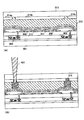
図3に、図2に示す画素部102をA−A’で切断した断面の概略構成を示す。図3において、基板301上には、下地層302として絶縁層が設けられ、その上にTFT303が形成されている。TFT303は、第1層間絶縁層304、第2層間絶縁層305によって覆われ、第2層間絶縁層305の上には、画素電極306が設けられている。下地層302や第1層間絶縁層304としては、酸化シリコン、窒化シリコンといった無機材料を用いることができる。また、第2層間絶縁層305としては、TFTによる第1層間絶縁層304の起伏を平坦化できるように、樹脂層を用いることが好ましい。樹脂材料としては、ポリイミド、ポリアミド、アクリル等の有機材料を用いても良い。一方、第1層間絶縁層304の起伏を良好に平坦化できる限りにおいては、第2層間絶縁層305として、酸化シリコン等の無機材料を用いても良い。
FIG. 3 shows a schematic configuration of a cross section obtained by cutting the
本実施形態に示す表示装置100は、発光素子307で発光した光を上方に出射する、いわゆるトップエミッション型の有機EL表示装置である。バンク308で区画された各画素には発光素子307が形成されている。発光素子307は、陽極として機能する画素電極306と陰極として機能する共通電極309で発光層310を挟み込んだ構造をとり、発光層310で発した光を画素電極306で上方に反射すると共に、共通電極309を透過させて矢印で示す方向に出射する構成となっている。
The
本実施形態の表示装置100においては、画素電極306は、反射率の高い金属膜で形成されていることが好ましいが、仕事関数の高い透明導電膜であるITO(IndiumTin Oxide)と金属膜との積層構造としてもよい。共通電極309は、透光性を有するITOやZnO(酸化亜鉛)等の透明導電膜で形成されていることが好ましい。なお、画素電極306の上に窒化シリコン膜等の保護膜を設けておくと、防水性の向上が期待できる。
In the
発光層310は、低分子又は高分子の有機材料を用いて形成することができる。勿論、発光層だけでなく、電子注入層、電子輸送層、正孔注入層、正孔輸送層といった各種機能層を設けることも可能であり、公知のあらゆる素子構造を採用することが可能である。また、発光層310として、有機材料のみならず、エレクトロルミネッセンス型の量子ドットを用いても良い。
The light-emitting
本実施形態の表示装置100は、共通電極309の上に封止膜311を設け、外部からの水分や大気の侵入を防ぎ、発光層310やTFT303の劣化を抑制している。そのため、封止膜311としては、緻密な膜質を備える窒化シリコン系の絶縁層を用いることが好ましい。さらに積層膜として、酸化シリコン系、酸化アルミニウム系の無機絶縁層や、樹脂系の有機絶縁層を設けても良い。
In the
封止膜311の上方には、対向基板を接着するための接着材として機能する樹脂層312(以下「充填層」という)を介して対向基板が設けられている。充填層312に用いる樹脂としては、十分な透明性と、封止膜311との密着性が得られるものであれば特に限定しない。対向基板は、基板313と基板313に形成されたRGB各色に対応するカラーフィルタ314a〜314cとで構成される。なお、図3には、赤(R)に対応するカラーフィルタ314a、緑(G)に対応するカラーフィルタ314b及び青(B)に対応するカラーフィルタ314cが示されている。
Above the
本実施形態において、充填層312は、発光素子307が形成された基板301と対向基板を構成する基板313とを貼り合わせるための接着層として機能すると共に、光増強層(Light Enhancement Layer:LEL)としても機能する。
In the present embodiment, the
その際、量子ドットは、充填層312内に均一に分散させることが好ましい。これにより、充填層312に対してどのような角度で進行した光も効率的に波長変換できるからである。勿論、基板面に対して水平方向と垂直方向とで量子ドットの密度が異なっていてもよく、充填層312内に量子ドットが所定の密度で存在していれば色変換層としての機能を果たすことができる。
At that time, the quantum dots are preferably dispersed uniformly in the packed
量子ドットとしては、数nm〜数十nmの大きさを有する化合物半導体や酸化物半導体の微粒子を用いることができる。例えば、InP、InN、CdSe、CdTe等の化合物半導体の微粒子が好ましい。また、微粒子の形状としては、略球体状のものが典型的であるが、一方に延びたロッド柱状とし、光学的に異方性をもたらすような形状であっても良い。これらの半導体微粒子は、量子井戸を形成することができ、外部から与えられた励起光を吸収して波長変換することにより、異なる波長の光を発することができるという特性をもつ。このような性質をもつ量子ドットは既に知られており、本実施形態の表示装置では、公知の量子ドットを用いることができる。 As the quantum dots, fine particles of a compound semiconductor or an oxide semiconductor having a size of several nanometers to several tens of nanometers can be used. For example, fine particles of a compound semiconductor such as InP, InN, CdSe, CdTe are preferable. The shape of the fine particles is typically a substantially spherical shape, but may be a rod column shape extending in one direction so as to provide optical anisotropy. These semiconductor fine particles can form quantum wells and have characteristics that light of different wavelengths can be emitted by absorbing the excitation light given from the outside and converting the wavelength. Quantum dots having such properties are already known, and known quantum dots can be used in the display device of this embodiment.
どのような波長を出力するか(すなわち、どのような色で発光するか)については、量子ドットの粒子の大きさによって調整することが可能である。したがって、粒子径の揃った量子ドットを充填層312内に分散させることで、スペクトルピークが鋭く、色純度の高い発光を得ることができる。この調整は、量子ドットを含む充填層312に対して、LELとしての機能に加え、色変換層(Color Conversion Material:CCM)としての機能ももたらす。そのため、充填層312内に量子ドットを分散させない構造に比べて、カラーフィルタの膜厚を薄くすることができる。
What wavelength is output (that is, in what color the light is emitted) can be adjusted by the size of the quantum dot particles. Therefore, by dispersing quantum dots having a uniform particle diameter in the packed
本実施形態の表示装置100では、発光層310として、青色光を発する有機EL材料を用い、その青色光を用いて量子ドットを励起することにより、赤色光及び緑色光を生成している。具体的には、赤色光を発する粒子径の量子ドットと緑色光を発する粒子径の量子ドットを混在させて分散させ、それぞれの量子ドットを励起し、量子ドットを中心に全方位に赤色光及び緑色光を発生させる。そして、発光層310で生成された青色光と、量子ドットにより充填層312内で生成された赤色光及び緑色光が、各画素に設けられたカラーフィルタ314a〜314cを通過して図3に示すようにRGB各色の光として出射される。なお、発光層310として、青色光の代わりに紫外光を発する有機EL材料を用いることも可能である。すなわち、発光素子307として、量子ドットを励起させるだけのエネルギーを持つ波長域の光を発する発光素子を用いればよい。
In the
また、本実施形態の表示装置100において、充填層312は、その一部が変質しており、その変質した部分の透過率は、その周囲の変質していない部分に比べ相対的に低くなっている。すなわち、充填層312には、互いに透過率の異なる領域が少なくとも二箇所以上存在する。本明細書中では、その変質した部分(図3において、符号315で示される部分)を「光遮蔽領域」と呼ぶこととする。光遮蔽領域315は、充填層312の一部(好ましくは、バンク308の上方)に対して選択的にエネルギー線(レーザー光、紫外光、電子線、赤外線等)を照射して形成することができる。そのため、光遮蔽領域315における量子ドットの密度とその周囲の変質していない領域における量子ドットの密度は同じである。
Further, in the
光遮蔽領域315の透過率は、低ければ低いほど光遮蔽効果が高まるが、周囲の領域(エネルギー線が照射されていない領域)の透過率の1/2以下であることが好ましい。透過率は、エネルギー線照射の条件によって種々変更できるので、所望の透過率となるように制御すれば良い。また、すべての光遮蔽領域315の透過率が同じである必要はなく、互いに透過率が異なる光遮蔽領域が複数設けられてもよい。
The lower the transmittance of the
以上のように、本実施形態の表示装置100は、充填層312の一部に形成された光遮蔽領域315によって各画素が区画されるため、発光素子307から発した光のうち隣接画素へ向かう光が光遮蔽領域315によって遮られ、隣接する画素内に漏れることを防ぐことができる。したがって、隣接画素への迷光によって混色が生じるといった問題を防ぐことができ、画質の改善された表示装置を実現することができる。
As described above, in the
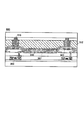
以下、上述した構成を備える本実施形態の表示装置100の製造工程について、図4を参照して述べる。
Hereinafter, the manufacturing process of the
<表示装置の製造方法>
図4に、本実施形態の表示装置100の製造工程を示す。図4(A)において、基板301上に公知の技術によりTFT303を形成した後、第1層間絶縁層304、第2層間絶縁層305を形成し、陽極として機能する画素電極306を形成する。さらに、画素電極306を形成した後、ポリイミドやアクリル等の樹脂材料を成膜し、パターニングを行ってバンク308を形成する。バンク308は、各画素を区画する隔壁として機能し、バンク308を形成していない部分が各画素の表示領域を構成することとなる。なお、TFT303の上方にバンク308を設けることにより、各画素の表示領域をできるだけ広く確保することが好ましい。
<Manufacturing method of display device>
FIG. 4 shows a manufacturing process of the
バンク308を形成した後、公知の方法により有機EL材料で構成される発光層310と、陰極として機能する共通電極309を形成する。本実施形態では、青色光を発する有機EL材料と、透光性を有する導電膜を順次成膜することにより、発光層310及び共通電極309を形成する。さらに、共通電極309上に封止膜311を形成してTFT基板(アクティブマトリクス基板)が完成する。
After forming the
TFT基板に貼り合わせる対向基板は、予め基板313上にカラーフィルタ314a〜314cをマトリクス状にパターニング形成して作製しておく。そして、TFT基板上(具体的には封止膜311上)に充填層312となるUV硬化樹脂を塗布し、TFT基板と対向基板とを接着する。その状態で紫外光(UV光)を照射してUV硬化樹脂を硬化させ、充填層312として機能させる。なお、本実施形態では、UV硬化樹脂を用いた例を示すが、接着層として機能する樹脂であれば、他の樹脂を用いることも可能である。
The counter substrate to be bonded to the TFT substrate is prepared in advance by forming
前述したように、充填層312には、量子ドット(QD)が分散している。充填層312内に量子ドットを分散させる方法としては、公知のUV硬化樹脂に予め混ぜておけば良い。その際、量子ドットに対して凝集抑制機能を付加できるような有機化合物を適宜選択して結合させることにより、UV硬化樹脂内に均一に分散させることができる。
As described above, quantum dots (QD) are dispersed in the
そして、充填層312を形成した後、図4(B)に示すように、充填層312の一部にエネルギー線401を照射して、充填層312の一部を変質させ、周囲の領域より透過率を低下させることにより光遮蔽領域315を形成する。エネルギー線としては、レーザ光、紫外光、電子線、赤外光等を用いることができる。
Then, after forming the
光遮蔽領域315は、バンク308上、すなわち画素と画素との間の境界に形成することが好ましい。これにより、互いに発光色の異なる画素を光遮蔽領域315によって区画できると共に、TFT303の上方に形成することで表示領域を最大限に確保することができる。また、各カラーフィルタ314a〜314cの隙間をバンク308上に合わせ、その隙間に対してエネルギー線401を照射することで、精度良く画素間の境界にエネルギー線401を照射することができる。
The
このとき、充填層312には量子ドットが混在しているため、量子ドットが混在していない場合に比べ、励起現象を利用してより短時間に透過率を低下させることが可能である。また、光遮蔽領域315の幅(図4(B)における横方向の幅)や透過率の値は、照射するエネルギー線401の強度や照射深度によって適宜調整することが可能である。
At this time, since the quantum dots are mixed in the packed
エネルギー線401の照射パターンは、少なくとも発光色の異なる画素間に光遮蔽領域315が形成できるようにすれば良い。図5(A)には、画素部に、RGBにそれぞれ対応する各画素501a〜501cをストライプ配列で形成した例を示す。この場合、ストライプに沿ってエネルギー線401を照射すれば隣接画素からの迷光による混色の問題を防ぐことができる。勿論、同一色の画素間に光遮蔽領域315を形成しても構わない。
The irradiation pattern of the
図5(B)には、各画素501a〜501cをデルタ配列で形成した例を示す。この場合、すべての画素間に対してエネルギー線401を照射すれば、隣接画素からの迷光による混色の問題を防ぐことができる。
FIG. 5B shows an example in which the
なお、図5(A)、(B)には、1本ずつエネルギー線を走査する例を示しているが、複数本のエネルギー線を用いて複数列を同時に処理してもよいし、マスクを用いて列ごと又は全体を一括照射してもよい。これらの処理は、いずれも製造工程のスループットを向上させる上で有効である。 5A and 5B show an example in which energy lines are scanned one by one. However, a plurality of columns may be processed simultaneously using a plurality of energy lines, and a mask may be used. It may be used to irradiate the whole column or the whole. All of these treatments are effective in improving the throughput of the manufacturing process.
さらに、本実施形態では、TFT基板と対向基板を貼り合わせた後にエネルギー線を照射する例を示したが、対向基板を貼り合わせる前に予め充填層にエネルギー線を照射して光遮蔽領域を形成しておいてもよい。このような例としては、例えば塗布された充填層に対し、対向基板の貼り合わせ前に、光遮蔽領域を形成すべき場所、つまり画素間の境界部分に対して局所的にエネルギー線の照射を行って予備硬化又は変質させた後で対向基板を貼り合わせ、その後全面に対してエネルギー線の照射を行って充填層を硬化させる等といった手順が挙げられる。 Furthermore, in this embodiment, an example in which energy rays are irradiated after the TFT substrate and the counter substrate are bonded is shown. However, before the counter substrate is bonded, the filling layer is irradiated with energy rays in advance to form a light shielding region. You may keep it. As an example of this, for example, before the counter substrate is bonded to the applied filling layer, energy rays are locally irradiated to a place where a light shielding region is to be formed, that is, a boundary portion between pixels. For example, the counter substrate is bonded after the preliminary curing or alteration, and the entire surface is then irradiated with energy rays to cure the filling layer.
このように、本発明の第1の実施形態に係る表示装置100は、充填層の一部にエネルギー線を照射して光遮蔽領域を形成することにより、製造工程を大幅に変更することなく、簡素な構成で隣接画素への光漏れを防止することができる。そのため、各画素間での混色を防ぎ、画質の改善された表示装置を実現することができる。
As described above, the
(第2の実施形態)
本発明の第2の実施形態に係る表示装置の構成について説明する。本実施の形態に係る表示装置は、図3に示す発光層310として、有機EL材料に代えて、量子ドットを含む樹脂材料を用いる。量子ドットについては、第1の実施形態で説明した量子ドットを用いれば良い。
(Second Embodiment)
A configuration of a display device according to the second embodiment of the present invention will be described. In the display device according to this embodiment, a resin material including quantum dots is used instead of the organic EL material as the light-emitting
本実施形態の表示装置における発光層は、公知の樹脂材料や無機材料に量子ドットを分散させた懸濁液を塗布した後、その懸濁液を硬化させて形成することができる。発光層は、電気エネルギーで量子ドットを励起し発光させるものでも、光エネルギーによって量子ドットを励起し発光させるものであっても良い。また、光エネルギーによって量子ドットを励起させる場合、量子ドットを分散させる材料としては、光が効率的に量子ドットに吸収されるように透光性材料を用いることが好ましい。 The light emitting layer in the display device of this embodiment can be formed by applying a suspension in which quantum dots are dispersed in a known resin material or inorganic material, and then curing the suspension. The light emitting layer may be one that excites quantum dots with electric energy to emit light, or one that excites quantum dots with light energy to emit light. In addition, when the quantum dots are excited by light energy, it is preferable to use a translucent material as a material for dispersing the quantum dots so that light is efficiently absorbed by the quantum dots.
本実施形態の表示装置は、発光素子から発した光の隣接画素内への漏れを防ぐことにより画素間での混色を防止するという効果に加えて、化学的に安定した材料を用いて発光層を形成することにより、表示装置の長寿命化を図ることができるという効果を有する。 In addition to the effect of preventing color mixing between pixels by preventing leakage of light emitted from the light emitting element into adjacent pixels, the display device of the present embodiment uses a chemically stable material to emit light. By forming the film, there is an effect that the life of the display device can be extended.
(第3の実施形態)
本発明の第3の実施形態に係る表示装置の構成について説明する。図6に、本実施形態に係る表示装置600における画素部の断面図を示す。図6において、図3と異なる点は、光遮蔽領域315の下方において発光層310に対してもエネルギー線の照射を行い、発光層を不活性化した不活性領域601を形成した点である。
(Third embodiment)
A configuration of a display device according to the third embodiment of the present invention will be described. FIG. 6 is a cross-sectional view of the pixel portion in the
なお、本明細書において、「発光層の不活性化」とは、発光層を変質させて高抵抗化することを意味する。すなわち、発光層310に対してエネルギー線を照射して、その照射部分を変質させ、照射部分以外の部分に比べて高抵抗な領域(不活性領域)を形成する。この場合、不活性領域601の電子移動度は、その他の部分(エネルギー線が照射されていない部分)の電子移動度に比べて低くなる。
In this specification, “inactivation of the light emitting layer” means that the light emitting layer is altered to increase resistance. That is, the
不活性領域601の形成は、光遮蔽領域315の形成と同時に行うことが製造工程の簡素化の観点から好ましいが、別々の工程としても良い。光遮蔽領域315と不活性領域601を同時に形成する場合、エネルギー線の照射深度を調整することにより1度の照射で同時に両者を形成することも可能であるし、エネルギー線の照射中に照射深度を変更することにより、同一位置で二段階に分けて照射することにより形成することも可能である。
The formation of the
本実施形態の表示装置600は、発光素子から発した光の隣接画素内への漏れを防ぐことにより画素間での混色を防止するという効果に加えて、発光層の一部に不活性領域を設けることにより、活性層を介した画素間のリーク電流を低減できるという効果を有する。
In addition to the effect of preventing color mixing between pixels by preventing leakage of light emitted from the light emitting element into adjacent pixels, the
本発明の構造は、前述した量子ドットを含む充填層を用いた表示装置に適用するのみならず、量子ドットを含まない一般的な充填層を発光層と対向基板との間に設けた表示装置の充填層に対して実施することで、光学的および電気的な混色防止の効果を同様に得ることができる。 The structure of the present invention is not only applied to the above-described display device using the filling layer containing quantum dots, but also a display device in which a general filling layer not containing quantum dots is provided between the light emitting layer and the counter substrate. By carrying out with respect to this filling layer, the effect of preventing optical and electrical color mixing can be obtained similarly.
100 表示装置
102 画素部
103 走査線駆動回路
104 データ線駆動回路
105 ドライバIC
201 画素
201a Rに対応する画素
201b Gに対応する画素
201c Bに対応する画素
202 TFT
203 バンク
301 TFT基板
302 下地層
303 TFT
304 第1層間絶縁層
305 第2層間絶縁層
306 画素電極
307 発光素子
308 バンク
309 共通電極
310 発光層
311 封止膜
312 充填層
313 基板
314a Rに対応するカラーフィルタ
314b Gに対応するカラーフィルタ
314c Bに対応するカラーフィルタ
315 光遮蔽領域
401 エネルギー線
501a Rに対応する画素
501b Gに対応する画素
501c Bに対応する画素
601 不活性領域
DESCRIPTION OF
201
304 First
Claims (17)
前記発光素子の前記第1基板とは反対の側に、複数の発光素子にまたがって位置し、量子ドットを含む樹脂層と、
を備え、
前記発光素子と重なる領域に位置する前記樹脂層は、第1透過率を有し、
前記複数の発光素子の境界の少なくとも一部に位置する前記樹脂層は、前記第1透過率よりも透過率が低い第2透過率を有する表示装置。 A first substrate provided with a plurality of light emitting elements;
A resin layer located on a side opposite to the first substrate of the light-emitting element and straddling a plurality of light-emitting elements and including quantum dots;
Bei to give a,
The resin layer located in a region overlapping with the light emitting element has a first transmittance,
The display device , wherein the resin layer located at least at a part of the boundary between the plurality of light emitting elements has a second transmittance that is lower than the first transmittance .
前記複数のカラーフィルタは、互いに隙間を介して離間しており、
前記樹脂層の前記第2透過率を有する領域は、前記隙間に対向することを特徴とする請求項1に記載の表示装置。 A second substrate provided with a plurality of color filters;
The plurality of color filters are separated from each other via a gap,
The display device according to claim 1 , wherein the region having the second transmittance of the resin layer faces the gap .
前記発光層の少なくとも一部は、前記複数の発光素子にまたがって位置し、且つ前記樹脂層の前記第2透過率を有する領域と対向する対向領域を有し、At least a part of the light emitting layer has an opposing region located across the plurality of light emitting elements and facing the region having the second transmittance of the resin layer,
前記対向領域は、前記発光層の前記少なくとも一部の、前記対向領域とは異なる領域よりも、抵抗が高いことを特徴とする請求項1から請求項8のいずれか1項に記載の表示装置。9. The display device according to claim 1, wherein the counter region has a higher resistance than a region of the at least part of the light emitting layer that is different from the counter region. .
前記樹脂層の一部にエネルギー線を照射して、該樹脂層の変質により他の部分に比べて透過率の低くなった領域を形成する工程と、
を備えたことを特徴とする表示装置の製造方法。 Bonding a first substrate provided with a plurality of light emitting elements and a second substrate provided with a plurality of color filters through a resin layer in which quantum dots are dispersed;
Irradiating part of the resin layer with energy rays to form a region having a lower transmittance than the other part due to alteration of the resin layer;
A method for manufacturing a display device, comprising:
前記樹脂層の前記一部は、前記隙間に対向することを特徴とする請求項10又は請求項11に記載の表示装置の製造方法。 The plurality of color filters are separated from each other via a gap,
The method for manufacturing a display device according to claim 10 , wherein the part of the resin layer faces the gap .
前記発光層の少なくとも一部は、前記複数の発光素子にまたがって位置し、且つ前記樹脂層の前記一部と対向する領域を有し、At least a part of the light emitting layer is located across the plurality of light emitting elements and has a region facing the part of the resin layer,
前記エネルギー線の照射により、前記樹脂層の前記一部と対向する前記領域を高抵抗化することを特徴とする請求項10から請求項16のいずれか1項に記載の表示装置の製造方法。The method for manufacturing a display device according to claim 10, wherein the region facing the part of the resin layer is increased in resistance by irradiation with the energy beam.
Priority Applications (1)
| Application Number | Priority Date | Filing Date | Title |
|---|---|---|---|
| JP2014166620A JP6404636B2 (en) | 2014-08-19 | 2014-08-19 | Display device |
Applications Claiming Priority (1)
| Application Number | Priority Date | Filing Date | Title |
|---|---|---|---|
| JP2014166620A JP6404636B2 (en) | 2014-08-19 | 2014-08-19 | Display device |
Publications (3)
| Publication Number | Publication Date |
|---|---|
| JP2016042450A JP2016042450A (en) | 2016-03-31 |
| JP2016042450A5 JP2016042450A5 (en) | 2017-09-07 |
| JP6404636B2 true JP6404636B2 (en) | 2018-10-10 |
Family
ID=55592109
Family Applications (1)
| Application Number | Title | Priority Date | Filing Date |
|---|---|---|---|
| JP2014166620A Active JP6404636B2 (en) | 2014-08-19 | 2014-08-19 | Display device |
Country Status (1)
| Country | Link |
|---|---|
| JP (1) | JP6404636B2 (en) |
Families Citing this family (3)
| Publication number | Priority date | Publication date | Assignee | Title |
|---|---|---|---|---|
| WO2023013013A1 (en) * | 2021-08-06 | 2023-02-09 | シャープ株式会社 | Light-emitting element, display device, and method for manufacturing light-emitting element |
| WO2023013012A1 (en) * | 2021-08-06 | 2023-02-09 | シャープ株式会社 | Electronic device and method of producing electronic device |
| WO2023013011A1 (en) * | 2021-08-06 | 2023-02-09 | シャープ株式会社 | Display device and method for manufacturing display device |
Family Cites Families (7)
| Publication number | Priority date | Publication date | Assignee | Title |
|---|---|---|---|---|
| JP2007225858A (en) * | 2006-02-23 | 2007-09-06 | Seiko Epson Corp | Manufacturing method of color filter substrate, manufacturing method of electroluminescence substrate, color filter substrate, electroluminescence substrate, electrooptical device and electronic equipment |
| US7932972B2 (en) * | 2006-10-02 | 2011-04-26 | Lg Display Co., Ltd. | Substrate for liquid crystal display device and method of fabricating the same |
| JP4752814B2 (en) * | 2007-06-21 | 2011-08-17 | パナソニック株式会社 | Organic device and manufacturing method thereof |
| JP2009087752A (en) * | 2007-09-28 | 2009-04-23 | Dainippon Printing Co Ltd | Light-emitting display element and light-emitting display panel |
| KR100951044B1 (en) * | 2007-10-17 | 2010-04-05 | 삼성코닝정밀유리 주식회사 | Method of manufacturing external light blocking film for display apparatus |
| JP5193957B2 (en) * | 2009-06-16 | 2013-05-08 | ローム株式会社 | Organic EL device and manufacturing method thereof |
| TW201427893A (en) * | 2013-01-07 | 2014-07-16 | 群康科技(深圳)有限公司 | Patterned color conversion film and display using the same |
-
2014
- 2014-08-19 JP JP2014166620A patent/JP6404636B2/en active Active
Also Published As
| Publication number | Publication date |
|---|---|
| JP2016042450A (en) | 2016-03-31 |
Similar Documents
| Publication | Publication Date | Title |
|---|---|---|
| US20180269260A1 (en) | Quantum dot array on directly patterned amoled displays and method of fabrication | |
| JP6131434B2 (en) | Color conversion layer, organic EL light emitting display panel having color conversion layer, and liquid crystal display panel | |
| KR102370715B1 (en) | Organic Light Emitting Diode Display Having Quantum Dot | |
| US10978676B2 (en) | Organic light-emitting display device | |
| KR101731164B1 (en) | Display device | |
| US10797115B2 (en) | Display panel and display apparatus using the same | |
| KR102119680B1 (en) | Display apparatus and method for driving the same | |
| JP6487173B2 (en) | Display device and manufacturing method thereof | |
| TWI537645B (en) | Display device | |
| WO2016140130A1 (en) | Electroluminescent device and manufacturing method | |
| JP6558880B2 (en) | Manufacturing method of organic EL display device | |
| EP2485567B1 (en) | Organic electroluminescence display apparatus | |
| JP2016042449A (en) | Display device | |
| JP2016048602A (en) | Display device | |
| JP2017091946A (en) | Display device and manufacturing method of display device | |
| JP6521610B2 (en) | Image display device | |
| US9362342B2 (en) | Light-emitting element display device | |
| KR101736646B1 (en) | Display device, method of manufacturing display device, and electronic apparatus | |
| KR102409702B1 (en) | Organic Light Emitting Diode Display Device | |
| JP6749160B2 (en) | Display device | |
| JP2017147059A (en) | Electro-optic device and electronic device | |
| KR20160026015A (en) | Display panel and manufacturing method of the same | |
| US8872415B2 (en) | Substrate, display panel, and display apparatus | |
| KR20220137580A (en) | Organic light emitting display device | |
| JP6404636B2 (en) | Display device |
Legal Events
| Date | Code | Title | Description |
|---|---|---|---|
| A521 | Request for written amendment filed |
Free format text: JAPANESE INTERMEDIATE CODE: A523 Effective date: 20170728 |
|
| A621 | Written request for application examination |
Free format text: JAPANESE INTERMEDIATE CODE: A621 Effective date: 20170728 |
|
| A977 | Report on retrieval |
Free format text: JAPANESE INTERMEDIATE CODE: A971007 Effective date: 20180629 |
|
| TRDD | Decision of grant or rejection written | ||
| A01 | Written decision to grant a patent or to grant a registration (utility model) |
Free format text: JAPANESE INTERMEDIATE CODE: A01 Effective date: 20180821 |
|
| A61 | First payment of annual fees (during grant procedure) |
Free format text: JAPANESE INTERMEDIATE CODE: A61 Effective date: 20180913 |
|
| R150 | Certificate of patent or registration of utility model |
Ref document number: 6404636 Country of ref document: JP Free format text: JAPANESE INTERMEDIATE CODE: R150 |
|
| R250 | Receipt of annual fees |
Free format text: JAPANESE INTERMEDIATE CODE: R250 |
|
| R250 | Receipt of annual fees |
Free format text: JAPANESE INTERMEDIATE CODE: R250 |
|
| R250 | Receipt of annual fees |
Free format text: JAPANESE INTERMEDIATE CODE: R250 |