WO2019044657A1 - 通電制御装置 - Google Patents
通電制御装置 Download PDFInfo
- Publication number
- WO2019044657A1 WO2019044657A1 PCT/JP2018/031178 JP2018031178W WO2019044657A1 WO 2019044657 A1 WO2019044657 A1 WO 2019044657A1 JP 2018031178 W JP2018031178 W JP 2018031178W WO 2019044657 A1 WO2019044657 A1 WO 2019044657A1
- Authority
- WO
- WIPO (PCT)
- Prior art keywords
- semiconductor switch
- power supply
- voltage
- load
- semiconductor
- Prior art date
- Legal status (The legal status is an assumption and is not a legal conclusion. Google has not performed a legal analysis and makes no representation as to the accuracy of the status listed.)
- Ceased
Links
Images


Classifications
-
- H—ELECTRICITY
- H03—ELECTRONIC CIRCUITRY
- H03K—PULSE TECHNIQUE
- H03K17/00—Electronic switching or gating, i.e. not by contact-making and –breaking
- H03K17/12—Modifications for increasing the maximum permissible switched current
- H03K17/122—Modifications for increasing the maximum permissible switched current in field-effect transistor switches
-
- H—ELECTRICITY
- H02—GENERATION; CONVERSION OR DISTRIBUTION OF ELECTRIC POWER
- H02H—EMERGENCY PROTECTIVE CIRCUIT ARRANGEMENTS
- H02H7/00—Emergency protective circuit arrangements specially adapted for specific types of electric machines or apparatus or for sectionalised protection of cable or line systems, and effecting automatic switching in the event of an undesired change from normal working conditions
- H02H7/20—Emergency protective circuit arrangements specially adapted for specific types of electric machines or apparatus or for sectionalised protection of cable or line systems, and effecting automatic switching in the event of an undesired change from normal working conditions for electronic equipment
-
- H—ELECTRICITY
- H02—GENERATION; CONVERSION OR DISTRIBUTION OF ELECTRIC POWER
- H02J—ELECTRIC POWER NETWORKS; CIRCUIT ARRANGEMENTS OR SYSTEMS FOR SUPPLYING OR DISTRIBUTING ELECTRIC POWER; SYSTEMS FOR STORING ELECTRIC ENERGY
- H02J7/00—Circuit arrangements for charging or discharging batteries or for supplying loads from batteries
- H02J7/60—Circuit arrangements for charging or discharging batteries or for supplying loads from batteries including safety or protection arrangements
-
- H—ELECTRICITY
- H03—ELECTRONIC CIRCUITRY
- H03K—PULSE TECHNIQUE
- H03K17/00—Electronic switching or gating, i.e. not by contact-making and –breaking
- H03K17/08—Modifications for protecting switching circuit against overcurrent or overvoltage
- H03K17/082—Modifications for protecting switching circuit against overcurrent or overvoltage by feedback from the output to the control circuit
- H03K17/0822—Modifications for protecting switching circuit against overcurrent or overvoltage by feedback from the output to the control circuit in field-effect transistor switches
-
- H—ELECTRICITY
- H03—ELECTRONIC CIRCUITRY
- H03K—PULSE TECHNIQUE
- H03K17/00—Electronic switching or gating, i.e. not by contact-making and –breaking
- H03K17/10—Modifications for increasing the maximum permissible switched voltage
- H03K17/102—Modifications for increasing the maximum permissible switched voltage in field-effect transistor switches
-
- H—ELECTRICITY
- H03—ELECTRONIC CIRCUITRY
- H03K—PULSE TECHNIQUE
- H03K17/00—Electronic switching or gating, i.e. not by contact-making and –breaking
- H03K17/51—Electronic switching or gating, i.e. not by contact-making and –breaking characterised by the components used
- H03K17/56—Electronic switching or gating, i.e. not by contact-making and –breaking characterised by the components used by the use, as active elements, of semiconductor devices
- H03K17/687—Electronic switching or gating, i.e. not by contact-making and –breaking characterised by the components used by the use, as active elements, of semiconductor devices the devices being field-effect transistors
-
- H—ELECTRICITY
- H03—ELECTRONIC CIRCUITRY
- H03K—PULSE TECHNIQUE
- H03K2217/00—Indexing scheme related to electronic switching or gating, i.e. not by contact-making or -breaking covered by H03K17/00
- H03K2217/0081—Power supply means, e.g. to the switch driver
Definitions
- the present invention relates to an energization control device.
- This application claims priority based on Japanese Patent Application No. 2017-167995 filed on Aug. 31, 2017, and incorporates all the contents described in the aforementioned Japanese application.
- the semiconductor switches of the energization control device described in Patent Document 1 are connected in parallel in the current path from the power supply to the load.
- the energization control device includes a drive circuit (drive circuit) for driving each of the semiconductor switches connected in parallel.
- the semiconductor switch described in Patent Document 1 is an n-channel FET, and a load is connected to the ground side with respect to the semiconductor switch. Since the on resistance of the semiconductor switch is generally very small compared to the resistance of the load, the voltage value of the voltage output from the power supply is substantially the same as the potential difference across the load, that is, the value of the voltage drop due to the load It becomes.
- the voltage value on the source side of the n-channel FET that is, the potential difference when the ground is a reference potential
- the voltage value on the source side of the n-channel FET is approximately equal to the voltage value of the voltage output from the power supply.
- the driving circuit performs boosting to generate a voltage obtained by adding the threshold voltage value to the voltage value on the source side, that is, a voltage higher than the voltage value output from the power supply, and the boosted voltage is generated by the n-channel FET. It is a circuit applied to the gate terminal and generally referred to as a bootstrap circuit.
- the energization control device includes a plurality of semiconductor switches provided between a power supply and a load and connected in parallel, and between the power supply and the load by turning on and off the semiconductor switch.
- the plurality of semiconductor switches include a first semiconductor switch and a second semiconductor switch, and the voltage is higher than a voltage value output from the power supply with respect to the first semiconductor switch. It is connected in series to a drive circuit that applies a voltage and is turned on, a switch control unit that turns on the second semiconductor switch, and a power supply side terminal of the second semiconductor switch, and applies a voltage applied to the terminal And a resistance for lowering.
- FIG. 1 is a block diagram showing a main configuration of a power supply system according to a first embodiment.
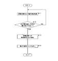
- 5 is a flowchart showing the processing procedure of the control unit according to the first embodiment.
- FIG. 7 is a block diagram showing a main configuration of a power supply system according to a second embodiment. It is a flowchart which shows the process sequence of the control part which concerns on Embodiment 2.
- FIG. 7 is a block diagram showing a main configuration of a power supply system according to a third embodiment. It is a flowchart which shows the process sequence of the control part which concerns on Embodiment 3.
- FIG. 1 is a block diagram showing a main configuration of a power supply system according to a first embodiment.
- 5 is a flowchart showing the processing procedure of the control unit according to the first embodiment.
- FIG. 7 is a block diagram showing a main configuration of a power supply system according to a second embodiment. It is a flowchart which shows the process sequence of the control part which concerns on Embodi
- An object of the present disclosure is to provide an energization control device that supplies power to a load even when a drive circuit that performs boosting is abnormal.
- an energization control apparatus for supplying power to a load even when a drive circuit that performs boosting is abnormal.
- a conduction control apparatus includes a plurality of semiconductor switches provided between a power supply and a load and connected in parallel, and the power supply and the load are switched by turning on and off the semiconductor switch. And a plurality of semiconductor switches including a first semiconductor switch and a second semiconductor switch, and a voltage value output from the power supply with respect to the first semiconductor switch. And a switch control unit for turning on the second semiconductor switch by applying a higher voltage than that of the second semiconductor switch, and a terminal on the power supply side of the second semiconductor switch connected in series and applied to the terminal And a resistor for lowering the voltage.
- the second semiconductor switch since a resistor is provided between the power supply side terminal of the second semiconductor switch and the connection node between the first semiconductor switch, the second semiconductor switch is turned on by a voltage drop due to the resistor.
- the switch control unit turns on the second semiconductor switch so that the voltage value to be applied is lower than the voltage value of the power supply. Therefore, when the first semiconductor switch is turned off, it is not necessary to boost the voltage to a voltage value higher than the voltage value of the power supply to turn on the second semiconductor switch, and the drive circuit that performs boosting becomes abnormal. Even the load can be powered.
- the current capacity of the second semiconductor switch is preferably smaller than the current capacity of the first semiconductor switch.
- the on resistance of the second semiconductor switch is preferably larger than the on resistance of the first semiconductor switch.
- the on resistance of the second semiconductor switch is larger than the on resistance of the first semiconductor switch, the combined resistance with the resistance connected in series with the on resistance of the second semiconductor switch The potential on the source side of the semiconductor switch can be further lowered. Therefore, when the first semiconductor switch is off, it is unnecessary to step up the voltage to a voltage value higher than the voltage value of the power supply in order to turn on the second semiconductor switch.
- the value of the voltage drop due to the resistance is larger than the threshold voltage for turning on the second semiconductor switch preferable.
- the value of the voltage drop due to the resistance is larger than the threshold voltage for turning on the second semiconductor switch, a voltage obtained by subtracting the value of the voltage drop due to the resistance from the voltage value of the power supply.
- the value obtained by adding the threshold voltage to the value is lower than the voltage value of the power supply. Therefore, it is unnecessary to step up the voltage to a voltage value higher than the voltage value of the power supply in order to turn on the second semiconductor switch.
- the configuration includes: an abnormality detection unit that detects an abnormality in the drive circuit; and a switch control unit that turns on the second semiconductor switch when the abnormality detection unit detects an abnormality in the drive circuit. .
- the second semiconductor switch has a voltage value of the power supply. As it can be turned on with the following voltage value, it is unnecessary to step up the voltage value higher than the voltage value of the power supply to turn on the second semiconductor switch. Therefore, even when the first semiconductor switch can not be turned on, the power of the power supply can be supplied to the load through the second semiconductor switch.
- a power supply system for supplying power to a load includes: a power supply; and a first semiconductor switch and a second semiconductor switch provided between the power supply and the load and connected in parallel; A drive circuit that applies a voltage higher than a voltage value output by the power supply to the first semiconductor switch, a control unit that turns on the second semiconductor switch, and a terminal on the power supply side of the second semiconductor switch And a resistor which drops the voltage applied to the terminal.
- the second semiconductor switch since a resistor is provided between the power supply side terminal of the second semiconductor switch and the connection node between the first semiconductor switch, the second semiconductor switch is turned on by a voltage drop due to the resistor.
- the switch control unit turns on the second semiconductor switch so that the voltage value to be applied is lower than the voltage value of the power supply. Therefore, when the first semiconductor switch is turned off, it is not necessary to boost the voltage to a voltage value higher than the voltage value of the power supply to turn on the second semiconductor switch, and the drive circuit that performs boosting becomes abnormal. Even the load can be powered.
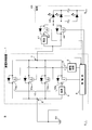
- FIG. 1 is a block diagram showing the main configuration of a power supply system S according to the first embodiment.
- the power supply system S includes the first power supply 20, the load 30, and the energization control device 1.
- the power supply system S is mounted on a vehicle (not shown) and supplies power from the first power supply 20 to an on-vehicle device serving as the load 30.
- the energization control device 1 is provided between the first power supply 20 and the load 30 and controls the supply and disconnection of power from the first power supply 20 to the load 30.
- the first power supply 20 is a secondary battery such as a lead battery or a lithium ion battery, and functions as, for example, a constant voltage power supply having an output voltage value of 12V.
- the load 30 is, for example, an on-vehicle device such as an interior light using a light emitting element such as an LED or a door lock mechanism using a DC motor.
- the energization control device 1 includes a plurality of semiconductor switches 10 in which a first semiconductor switch 10a and a second semiconductor switch 10b are connected in parallel, a drive circuit 2 for turning on the first semiconductor switch 10a, and a plurality of semiconductor switches
- the control unit 5 outputs a control signal for turning 10 on or off.
- the first semiconductor switch 10 a is an n-channel FET (field effect transistor). Three first semiconductor switches 10a are connected in parallel.
- the first semiconductor switch 10a is not limited to the n-channel FET, and may be an npn-channel bipolar transistor or an n-channel IGBT (insulated gate bipolar transistor).
- the number in parallel of the first semiconductor switches 10a is not limited to three, and is appropriately determined by the current value flowing through the first semiconductor switches 10a and the electrical characteristics such as the on resistance or the maximum drain current of the first semiconductor switches 10a. .
- the second semiconductor switch 10 b is an n-channel FET.
- One second semiconductor switch 10b is connected in parallel, similarly to the three first semiconductor switches 10a. Therefore, the plurality of semiconductor switches 10 are connected in four parallel.
- the second semiconductor switch 10b is not limited to the n-channel FET, and may be an npn-channel bipolar transistor or an n-channel IGBT.
- the number of second semiconductor switches 10b is not limited to one, and is appropriately determined according to the current value flowing to the second semiconductor switch 10b and the electrical characteristics such as the on resistance or the maximum drain current of the second semiconductor switches 10b.
- the second semiconductor switch 10b is connected in parallel in the same manner as the first semiconductor switch 10a, depending on the number of parallel connections according to the number of switches.
- the resistor 4 described later is connected in series to the power supply side of the second semiconductor switch 10b, the current capacity of the second semiconductor switch 10b is smaller than the current capacity of the first semiconductor switch 10a. Therefore, an inexpensive semiconductor switch can be used as the second semiconductor switch 10b. Further, the on resistance of the second semiconductor switch 10 b is a resistance value higher than the on resistance of the first semiconductor switch 10 a.
- the drain terminals of the plurality of semiconductor switches 10 are connected to the first power supply 20, and the source terminals are connected to the load 30. Therefore, the first power supply side connection node 6, which is a connection node on the first power supply 20 side of the first semiconductor switch 10a and the second semiconductor switch 10b, is located on the drain terminal side.
- the load-side connection node 7 serving as the connection node on the load 30 side of the first semiconductor switch 10 a and the second semiconductor switch 10 b is located on the source terminal side.
- the drive circuit 2 is provided between the control unit 5 and the gate terminal of each of the first semiconductor switches 10a.
- the drive circuit 2 and each gate terminal are connected by the electric wire branched in parallel according to the number of gate terminals. Therefore, the three first semiconductor switches 10a can be simultaneously turned on by the single drive circuit 2, and a simple circuit configuration can be achieved.
- the drive circuit 2 applies a voltage for turning on the first semiconductor switch 10 a to the gate terminals of the first semiconductor switches 10 a based on the control signal output from the control unit 5.
- the drive circuit 2 has a boosting function.
- the voltage value for turning on the first semiconductor switch 10a needs a higher voltage than the voltage value of the source terminal of the first semiconductor switch 10a by the threshold voltage determined by the characteristics of the first semiconductor switch 10a. It is assumed. Since the load 30 is provided between the first semiconductor switch 10a and the ground serving as the reference potential, the voltage value of the source terminal is substantially the same as the voltage value of the drain terminal, that is, the output voltage value of the first power supply 20. It becomes. Therefore, the drive circuit 2 boosts the voltage so as to be higher by the threshold voltage than the output voltage value of the first power supply 20, and applies the boosted voltage to the gate terminal of the first semiconductor switch 10a.
- the control unit 5 has a CPU (central processing unit), and executes control processing by executing a control program stored in a ROM (Read Only Memory) (not shown).
- the control unit 5 controls the plurality of semiconductor switches 10 to turn on or off based on an instruction from a body ECU (Electronic Control Unit) (not shown) that controls the entire vehicle, for example, and between the first power supply 20 and the load 30. Control the current flow.
- the control unit 5 corresponds to a switch control unit and an abnormality detection unit.
- the control unit 5 When supplying power to the load 30, the control unit 5 simultaneously turns on the plurality of semiconductor switches 10 including the first semiconductor switch 10a and the second semiconductor switch 10b.
- the control unit 5 When the first semiconductor switch 10 a is turned on, the control unit 5 outputs a control signal to the drive circuit 2.
- the control unit 5 When the second semiconductor switch 10b is turned on, the control unit 5 outputs a control signal to the second semiconductor switch 10b. Since the plurality of semiconductor switches 10 are connected in parallel, it is possible to reduce the resistance value of the combined resistance formed of the on resistances of the plurality of semiconductor switches 10. Further, since the current can be divided according to the number of parallel connections, the value of the current flowing in each of the plurality of semiconductor switches 10 can be reduced.
- control unit 5 may turn on the first semiconductor switch 10a and turn off the second semiconductor switch 10b. Since a resistor 4 described later is connected in series to the second semiconductor switch 10b, the heat loss due to the resistor 4 can be suppressed by turning on only the first semiconductor switch 10a.
- the drive voltage detection unit 3 detects the voltage value of the voltage applied from the drive circuit 2 to the gate terminal of the first semiconductor switch 10 a and outputs the voltage value to the control unit 5.
- the control unit 5 acquires the voltage value detected by the drive voltage detection unit 3 and determines whether the acquired voltage value is boosted to a voltage value for turning on the first semiconductor switch 10a.
- An abnormality in the drive circuit 2 is detected.
- the current value flowing through the first semiconductor switch 10a, the potential difference between the drain terminal and the source terminal of the first semiconductor switch 10a, or the voltage of the source terminal (potential difference between the source terminal and the ground serving as the reference potential) is detected.
- a detector may be provided.
- the detection unit may output the detection result to the control unit 5, and the control unit 5 may detect an abnormality of the drive circuit 2 based on the detected value of the current value or the like.
- the control unit 5 outputs a control signal to the drive circuit 2 to turn on the first semiconductor switch 10a, if the value of the current flowing through the first semiconductor switch 10a is smaller than a predetermined value, driving is performed.
- the boosting by circuit 2 is not sufficient.
- a resistor 4 is connected in series between the second semiconductor switch 10 b and the first power supply side connection node 6. In the state where the first semiconductor switch 10a is turned off and the second semiconductor switch 10b is turned on, the resistance of the resistor 4 is larger than the threshold voltage for turning on the second semiconductor switch 10b.
- the resistance value of 4 is set.
- the resistor 4 and the second semiconductor switch may be configured such that the value of the voltage drop due to the combined resistance of the resistor 4 and the on-resistance of the second semiconductor switch 10b is larger than the threshold voltage for turning on the second semiconductor switch 10b.
- Each resistance value of 10b may be set.
- the resistance value of the resistor 4 is 49 ⁇
- the resistance value of the on resistance of the second semiconductor switch 10b is 0.5 ⁇
- the load 30 is a circuit configured by a light emitting element 42 such as an LED, for example, and the voltage drop is 2V. In this case, the voltage of approximately 9.9 V is dropped by the resistor 4 by outputting a voltage of 12 V from the first power supply 20.
- the threshold voltage of the second semiconductor switch 10b is, for example, 2 V, and the value of the voltage drop is larger than the threshold voltage of the second semiconductor switch 10b.
- the second semiconductor switch 10b is turned on by applying to the gate terminal of the second semiconductor switch 10b a voltage of about 4 V obtained by adding 2 V of the threshold voltage to 2 V which is the source side voltage of the second semiconductor switch 10b. can do. Since the control unit 5 is electrically connected to the first power supply 20, the control unit 5 can output a voltage lower than the voltage output from the first power supply 20.
- the second semiconductor switch 10b can be turned on by a voltage having a voltage value lower than the voltage output from the first power supply 20, and it is not necessary to boost the voltage to a voltage higher than the voltage output from the first power supply 20 It can be done.
- the second semiconductor switch 10b is turned on without using the drive circuit 2 having a boosting function, and the first power supply 20 and the load 30 are energized,
- the power supply 20 can supply power to the load 30.
- the first semiconductor switch 10 a when the first semiconductor switch 10 a is turned off and the second semiconductor switch 10 b is turned on, the value of the current flowing to the load 30 side is reduced by the resistor 4. Therefore, if a failure such as a short circuit is suspected on the load 30 side, the first semiconductor switch 10a is turned off and the second semiconductor switch 10b is turned on to turn the current (small current) having a small current value to the load 30 side. It is possible to perform fault diagnosis such as identification of a short circuit location or an energization inspection while preventing flow and large current flow.
- FIG. 2 is a flowchart showing the processing procedure of the control unit 5 according to the first embodiment.
- the control unit 5 of the energization control device 1 constantly executes the processing procedure described below.
- the control unit 5 acquires the voltage value of the voltage output from the drive circuit 2 to the gate terminal of the first semiconductor switch 10a (S11).
- the control unit 5 determines whether the acquired voltage value is lower than a predetermined voltage value, that is, a voltage value for turning on the first semiconductor switch 10a (S12).
- a predetermined voltage value that is, a voltage value for turning on the first semiconductor switch 10a (S12).
- S12 a voltage value for turning on the first semiconductor switch 10a
- the control unit 5 detects an abnormality in the drive circuit 2. If the acquired voltage value is lower than the predetermined voltage value, it means that the boosting by the drive circuit 2 is not sufficient. Therefore, although the control signal for turning on the first semiconductor switch 10a is output from the control unit 5 to the drive circuit 2, if the acquired voltage value is lower than the predetermined voltage value, the drive is performed. Circuit 2 is abnormal. The control unit 5 stops the output of the control signal to the drive circuit 2 for turning on the first semiconductor switch 10a (S13). By stopping the output of the control signal to the drive circuit 2, the first semiconductor switch 10a is turned off.
- the control unit 5 outputs a control signal for turning on the second semiconductor switch 10b (S14).
- the control signal output from the controller 5 to the second semiconductor switch 10b is a voltage applied to the gate terminal of the second semiconductor switch 10b in order to turn on the second semiconductor switch 10b.
- the voltage value of the voltage applied to the gate terminal of the second semiconductor switch 10b is a voltage value obtained by adding the threshold voltage of the second semiconductor switch 10b to the voltage value on the source terminal side of the second semiconductor switch 10b.
- the value of the voltage drop of the resistor 4 connected in series to the first power supply 20 side of the second semiconductor switch 10 b is larger than the threshold voltage of the second semiconductor switch 10 b, and therefore, is higher than the voltage output from the first power supply 20. The low voltage can turn on the second semiconductor switch 10b.
- the second semiconductor switch 10b can be turned on, and the first Power can be supplied from the power supply 20 to the load 30.
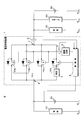
- FIG. 3 is a block diagram showing the main configuration of a power supply system S according to a second embodiment.
- the second embodiment includes the lighting circuit 40 as the load 30, and the control unit 5 outputs the control signal for lighting or extinguishing the lighting circuit 40 in the same manner as the energization control device 1 of the first embodiment.
- the other configurations and effects are the same as those of the first embodiment, and therefore the corresponding portions are denoted by the same reference numerals and the detailed description will be omitted.
- the lighting circuit 40 includes a light emitting element 42 such as an LED, and a third semiconductor switch 43 and a fourth semiconductor switch 44 connected in parallel to turn on or off the light emitting element 42. Used.
- the third semiconductor switch 43 and the fourth semiconductor switch 44 are n-channel FETs.
- the third semiconductor switch 43 and the fourth semiconductor switch 44 are not limited to the n-channel FET, and may be an n-channel bipolar transistor, an n-channel IGDP or a p-channel semiconductor switch.
- the on resistance of the third semiconductor switch 43 is, for example, 0.002 ⁇
- the on resistance of the fourth semiconductor switch 44 is, for example, 0.5 ⁇ .
- a light emitting element 42 is provided between the ground and a connection node at the ground (reference potential) side of the third semiconductor switch 43 and the fourth semiconductor switch 44. For example, when a current of 20 mA is applied, a voltage drop of 2 V occurs, and ten light emitting elements 42 are connected in parallel (not shown). Therefore, the sum of the current values flowing to the ten LEDs is 0.2A.
- a resistor in the lighting circuit 41 is connected in series with the third semiconductor switch 43 between the third semiconductor switch 43 and the connection node between the third semiconductor switch 43 and the fourth semiconductor switch 44 on the side of the energizing device. is there.
- a current of 0.2 A is caused to flow to the LED by the voltage of 12 V output from the first power supply 20.
- the control unit 5 turns on the third semiconductor switch 43 of the lighting circuit 40 when the first power supply 20 and the lighting circuit 40 are energized via the first semiconductor switch 10a without detecting any abnormality in the driving circuit 2. , And the fourth semiconductor switch 44 is turned off.
- the controller 5 detects an abnormality in the drive circuit 2 and turns on the second semiconductor switch 10b when the first semiconductor switch 10a can not be turned on, and the first power supply 20 and the lighting circuit 40 via the second semiconductor switch 10b. And power on. Then, the control unit 5 turns off the third semiconductor switch 43 of the lighting circuit 40 and turns on the fourth semiconductor switch 44.
- the combined resistance due to the on resistance 44 determines the value of the current flowing through the light emitting element 42.
- the resistance value of the combined resistance can be 50 ⁇ , and the current value flowing to the light emitting element 42 can be 0.2A.
- the voltage for turning on the second semiconductor switch 10b is set to a voltage value lower than the voltage output by the first power supply 20 due to the voltage drop due to the resistor 4 connected in series to the second semiconductor switch 10b. It is possible to eliminate the need for boosting the voltage output by the first power supply 20.
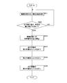
- FIG. 4 is a flowchart illustrating the processing procedure of the control unit 5 according to the second embodiment.
- the control unit 5 of the energization control device 1 constantly executes the processing procedure described below.
- the processes of S21 to S23 are the same as the processes of S11 to S13 of the first embodiment, and thus the description thereof is omitted.
- the control unit 5 stops the output of the control signal of the third semiconductor switch 43 of the lighting circuit 40 (S24). As in the first embodiment, the control unit 5 turns on the second semiconductor switch 10b of the energization control device 1 (S25). The control unit 5 outputs a control signal to the fourth semiconductor switch 44 of the lighting circuit 40 to turn on the fourth semiconductor switch 44 (S26).
- a constant current of 20 mA is supplied as a forward current to the light emitting element 42 such as an LED, and the resistance 41 in the lighting circuit of the lighting circuit 40 and the resistance 4 of the energization control device 1
- An appropriate forward current can be determined by setting the resistance value of the resistance value to approximately the same resistance value.
- the first semiconductor switch 10 a is turned on by controlling the third semiconductor switch 43 and the fourth semiconductor switch 44 of the lighting circuit 40 in conjunction with the control of the first semiconductor switch 10 a and the second semiconductor switch 10 b. Even when the drive circuit 2 for performing the operation becomes abnormal, power can be supplied from the first power supply 20 to the lighting circuit 40, and the lighting circuit 40 can be lit.
- FIG. 5 is a block diagram showing the main configuration of a power supply system S according to a third embodiment.
- the third embodiment has the same configuration as the current control device 1 of the first embodiment except that the current control device 1 includes the voltage detection unit 8 that detects the voltage of the load-side connection node 7.
- the power supply system S includes a second power supply 50 and a starter 60 connected in parallel to the load 30 on the load 30 side. Further, on the side of the first power supply 20 of the power supply system S, a first power supply side load 70 is connected in parallel to the first power supply 20.
- the other configurations and effects are the same as those of the first embodiment, and therefore the corresponding portions are denoted by the same reference numerals and the detailed description will be omitted.
- the second power supply 50 is connected in parallel to the load 30 on the load 30 side, and is a secondary battery such as a lead battery or a lithium ion battery like the first power supply 20.
- the output voltage value is 12 V Function as a constant voltage power supply for
- the voltage value of the voltage output by the second power supply 50 is substantially the same as the voltage value of the voltage output by the first power supply 20.
- the starter 60 is connected in parallel with the load 30 and the second power supply 50 on the load 30 side, and starts the vehicle engine by the power shared by the second power supply 50. Since the starter 60 requires a large amount of current when starting the engine, voltage fluctuation of the second power supply 50 occurs. Therefore, the control unit 5 turns off the plurality of semiconductor switches 10 to prevent the first power supply 20 and the first power supply side load 70 from being affected by the voltage fluctuation on the second power supply 50 side. And the second power supply 50 are cut off. After the voltage of the second power supply 50 is recovered, the control unit 5 turns on the plurality of semiconductor switches 10 to connect the first power supply 20 and the second power supply 50.
- the voltage detection unit 8 detects the voltage of the load-side connection node 7, and outputs the detected voltage value to the control unit 5. Based on the acquired voltage value, the control unit 5 determines whether the voltage of the load-side connection node 7, that is, the voltage value of the voltage output by the second power supply 50 is equal to or less than a predetermined voltage value. In the case, the second semiconductor switch 10b is turned on.
- FIG. 6 is a flowchart illustrating the processing procedure of the control unit 5 according to the third embodiment.
- the control unit 5 of the energization control device 1 constantly executes the processing procedure described below. Since the processes from S31 to S33 are the same as the processes from S11 to S13 of the first embodiment, the description will be omitted.
- the control unit 5 acquires the voltage of the load-side connection node 7, that is, the voltage value of the voltage output by the second power supply 50 (S34). The control unit 5 determines whether the acquired voltage value is less than or equal to a predetermined voltage value (S35).
- the predetermined voltage value is, for example, a discharge termination voltage which is a characteristic of the second power supply 50.
- the discharge termination voltage is a voltage value in a state where the second power source 50 can not discharge any more because the storage capacity stored in the second power source 50 is reduced. Therefore, when the voltage of the second power supply 50 decreases to the discharge termination voltage, the power can not be supplied from the second power supply 50 to the load 30.
- the control unit 5 If the acquired voltage value is not less than or equal to the predetermined voltage value (S35: NO), the control unit 5 returns to the process of S34. If the acquired voltage value is less than or equal to the predetermined voltage value (S35: YES), the control unit 5 turns on the second semiconductor switch 10b (S36).
- S power supply system 1 energization control device 10 semiconductor switch 10a first semiconductor switch 10b second semiconductor switch 2 drive circuit 3 drive voltage detection unit 4 resistance 5 control unit (switch control unit, abnormality detection unit) 6 1st power supply side connection node (power supply side connection node) 7 load side connection node 8 voltage detection unit 20 first power supply (power supply) 30 load 40 lighting circuit (load) DESCRIPTION OF SYMBOLS 41 Light-emitting circuit resistance 42 Light emitting element 43 3rd semiconductor switch 44 4th semiconductor switch 50 2nd power supply 60 starter 70 1st power supply side load
Landscapes
- Engineering & Computer Science (AREA)
- Power Engineering (AREA)
- Electronic Switches (AREA)
- Protection Of Static Devices (AREA)
Abstract
通電制御装置は、電源と負荷との間に設けられ、並列に接続されている複数の半導体スイッチを有し、該半導体スイッチのオンオフにより、前記電源と負荷との間の通電を制御する。前記複数の半導体スイッチは、第1半導体スイッチ及び第2半導体スイッチを含む。通電制御装置は、前記第1半導体スイッチに対して、前記電源が出力する電圧値よりも高い電圧を印加してオン動作させる駆動回路と、前記第2半導体スイッチをオン動作させるスイッチ制御部と、前記第2半導体スイッチの電源側の端子に直列に接続され、該端子に印加される電圧を降下させる抵抗とを備える。
Description
本発明は、通電制御装置に関する。
本出願は、2017年8月31日出願の日本出願第2017-167995号に基づく優先権を主張し、前記日本出願に記載された全ての記載内容を援用するものである。
本出願は、2017年8月31日出願の日本出願第2017-167995号に基づく優先権を主張し、前記日本出願に記載された全ての記載内容を援用するものである。
現在、車両には、電源(バッテリ)から通電される車内灯、ヒータ又はワイパー等の多数の電気機器(負荷)が搭載されている。電源から負荷への通電、すなわち電力の供給は、通電制御装置(電力供給制御装置)によって制御されている(特許文献1を参照)。
特許文献1に記載の通電制御装置の半導体スイッチは、電源から負荷に至る電流経路に並列に接続してある。そして、当該通電制御装置は、並列に接続されている半導体スイッチ夫々を駆動するための駆動回路(ドライブ回路)を備えている。
特許文献1に記載の半導体スイッチは、nチャネル型FETであり、負荷は、半導体スイッチに対してグランド側に接続されている。半導体スイッチのオン抵抗は、一般的に負荷の抵抗に比べると極めて小さいため、電源から出力される電圧の電圧値は、当該負荷の両端における電位差、すなわち当該負荷による電圧降下の値と略同じ値となる。
従って、nチャネル型FETのソース側の電圧値、すなわちグランドを基準電位とした場合の電位差は、電源から出力される電圧の電圧値と、略等しくなる。nチャネル型FETである半導体スイッチをオンにするためには、ソース側の電圧値に、当該半導体スイッチの特性によって決定される閾値電圧を加えた電圧をnチャネル型FETのゲート端子に印加する必要がある。駆動回路は、昇圧を行うことによって、ソース側の電圧値に閾値電圧値を加えた電圧、すなわち電源から出力された電圧値よりも高い電圧を生成し、当該昇圧した電圧をnチャネル型FETのゲート端子に印加する回路であり、一般的にブートストラップ回路と称される。
本開示の一態様に係る通電制御装置は、電源と負荷との間に設けられ、並列に接続されている複数の半導体スイッチを有し、該半導体スイッチのオンオフにより、前記電源と負荷との間の通電を制御する通電制御装置であって、前記複数の半導体スイッチは、第1半導体スイッチ及び第2半導体スイッチを含み、前記第1半導体スイッチに対して、前記電源が出力する電圧値よりも高い電圧を印加してオン動作させる駆動回路と、前記第2半導体スイッチをオン動作させるスイッチ制御部と、前記第2半導体スイッチの電源側の端子に直列に接続され、該端子に印加される電圧を降下させる抵抗とを備える。
[本開示が解決しようとする課題]
駆動回路を各半導体スイッチに対応して設けるためには、半導体スイッチの個数分の駆動回路が必要となり、回路構成が複雑となる。また、各半導体スイッチに対し単一の駆動回路を設け、当該単一の駆動回路からの出力を並列に分流して、各半導体スイッチに電圧を印加する構成とした場合、当該単一の駆動回路が異常となった際には、昇圧を行うことができず、いずれの半導体スイッチもオンにすることができない。
駆動回路を各半導体スイッチに対応して設けるためには、半導体スイッチの個数分の駆動回路が必要となり、回路構成が複雑となる。また、各半導体スイッチに対し単一の駆動回路を設け、当該単一の駆動回路からの出力を並列に分流して、各半導体スイッチに電圧を印加する構成とした場合、当該単一の駆動回路が異常となった際には、昇圧を行うことができず、いずれの半導体スイッチもオンにすることができない。
本開示の目的は、昇圧を行う駆動回路が異常となった場合であっても、負荷に電力を供給する通電制御装置を提供する。
[本開示の効果]
本開示によれば、昇圧を行う駆動回路が異常となった場合であっても、負荷に電力を供給する通電制御装置を提供する。
本開示によれば、昇圧を行う駆動回路が異常となった場合であっても、負荷に電力を供給する通電制御装置を提供する。
[本発明の実施形態の説明]
最初に本開示の実施態様を列挙して説明する。また、以下に記載する実施形態の少なくとも一部を任意に組み合わせてもよい。
最初に本開示の実施態様を列挙して説明する。また、以下に記載する実施形態の少なくとも一部を任意に組み合わせてもよい。
(1)本開示の一態様に係る通電制御装置は、電源と負荷との間に設けられ、並列に接続されている複数の半導体スイッチを有し、該半導体スイッチのオンオフにより、前記電源と負荷との間の通電を制御する通電制御装置であって、前記複数の半導体スイッチは、第1半導体スイッチ及び第2半導体スイッチを含み、前記第1半導体スイッチに対して、前記電源が出力する電圧値よりも高い電圧を印加してオン動作させる駆動回路と、前記第2半導体スイッチをオン動作させるスイッチ制御部と、前記第2半導体スイッチの電源側の端子に直列に接続され、該端子に印加される電圧を降下させる抵抗とを備える。
本態様にあっては、第2半導体スイッチの電源側の端子と、第1半導体スイッチとの接続節点間には、抵抗が設けられているので、抵抗による電圧降下によって、第2半導体スイッチをオンにするために印加する電圧値を電源の電圧値よりも低くし、スイッチ制御部は、第2半導体スイッチをオン動作させる。従って、第1半導体スイッチがオフの場合、第2半導体スイッチをオンにするために、電源の電圧値よりも高い電圧値に昇圧することを不要とし、昇圧を行う駆動回路が異常となった場合であっても、負荷に電力を供給することができる。
(2)前記第2半導体スイッチの電流容量は、前記第1半導体スイッチの電流容量よりも小さい構成が好ましい。
本態様にあっては、第2半導体スイッチの電源側の端子と、第1半導体スイッチとの接続節点間には、抵抗が設けられているので、当該抵抗によって、第2半導体スイッチに流れる電流は小さくなる。従って、第1半導体スイッチの電流容量よりも小さい電流容量の半導体スイッチを、第2半導体スイッチに使用することで、安価な通電制御装置を提供することができる。
(3)前記第2半導体スイッチのオン抵抗は、前記第1半導体スイッチのオン抵抗よりも大きい構成が好ましい。
本態様にあっては、第2半導体スイッチのオン抵抗は、第1半導体スイッチのオン抵抗よりも大きいので、第2半導体スイッチのオン抵抗と直列に接続してある抵抗との合成抵抗によって、第2半導体スイッチのソース側の電位を更に下げるができる。従って、第1半導体スイッチがオフの場合、第2半導体スイッチをオンにするために、電源の電圧値よりも高い電圧値に昇圧することを不要とすることができる。
(4)前記第1半導体スイッチをオフにし、前記第2半導体スイッチをオンにした状態において、前記抵抗による電圧降下の値は、前記第2半導体スイッチをオンにするための閾値電圧より大きい構成が好ましい。
本態様にあっては、抵抗による電圧降下の値は、第2半導体スイッチをオンにするための閾値電圧より大きくしてあるので、電源の電圧値から、抵抗による電圧降下の値を減算した電圧値に、閾値電圧を加算した電圧値は、電源の電圧値よりも低くなる。従って、第2半導体スイッチをオンにするために電源の電圧値よりも高い電圧値に昇圧することを不要とすることができる。
(5)前記駆動回路の異常を検出する異常検出部と、前記異常検出部によって、前記駆動回路の異常を検出した場合、前記第2半導体スイッチをオンにするスイッチ制御部とを備える構成が好ましい。
本態様にあっては、前記駆動回路の異常によって電源の電圧を昇圧できず、前記第1半導体スイッチをオンにすることができない場合であっても、前記第2半導体スイッチは、電源の電圧値以下の電圧値でオンにすることができるため、第2半導体スイッチをオンにするために電源の電圧値よりも高い電圧値に昇圧することを不要とすることができる。従って、前記第1半導体スイッチをオンにすることができない場合であっても、第2半導体スイッチを介して、電源の電力を負荷に供給することができる。
(6)本開示の一態様に係る負荷に電力を供給する電源システムは、電源と、電源と負荷との間に設けられ、並列に接続されている第1半導体スイッチ及び第2半導体スイッチと、前記第1半導体スイッチに対して、前記電源が出力する電圧値よりも高い電圧を印加する駆動回路と、前記第2半導体スイッチをオン動作させる制御部と、前記第2半導体スイッチの電源側の端子に直列に接続され、該端子に印加される電圧を降下させる抵抗とを備える。
本態様にあっては、第2半導体スイッチの電源側の端子と、第1半導体スイッチとの接続節点間には、抵抗が設けられているので、抵抗による電圧降下によって、第2半導体スイッチをオンにするために印加する電圧値を電源の電圧値よりも低くし、スイッチ制御部は、第2半導体スイッチをオン動作させる。従って、第1半導体スイッチがオフの場合、第2半導体スイッチをオンにするために、電源の電圧値よりも高い電圧値に昇圧することを不要とし、昇圧を行う駆動回路が異常となった場合であっても、負荷に電力を供給することができる。
[本発明の実施形態の詳細]
本開示の実施態様に係る通電制御装置の具体例を、以下に図面を参照しつつ説明する。なお、本発明はこれらの例示に限定されるものではなく、請求の範囲によって示され、請求の範囲と均等の意味および範囲内でのすべての変更が含まれることが意図される。
本開示の実施態様に係る通電制御装置の具体例を、以下に図面を参照しつつ説明する。なお、本発明はこれらの例示に限定されるものではなく、請求の範囲によって示され、請求の範囲と均等の意味および範囲内でのすべての変更が含まれることが意図される。
(実施形態1)
以下、実施の形態について図面に基づいて説明する。図1は、実施形態1に係る電源システムSの要部構成を示すブロック図である。電源システムSは、第1電源20、負荷30及び通電制御装置1を備え、例えば車両(図示せず)に搭載され、負荷30となる車載装置に対し、第1電源20からの電力を供給する。通電制御装置1は、第1電源20と負荷30との間に設けられてあり、第1電源20から負荷30への電力の給断を制御する。
以下、実施の形態について図面に基づいて説明する。図1は、実施形態1に係る電源システムSの要部構成を示すブロック図である。電源システムSは、第1電源20、負荷30及び通電制御装置1を備え、例えば車両(図示せず)に搭載され、負荷30となる車載装置に対し、第1電源20からの電力を供給する。通電制御装置1は、第1電源20と負荷30との間に設けられてあり、第1電源20から負荷30への電力の給断を制御する。
第1電源20は、鉛バッテリ又はリチウムイオンバッテリ等の二次電池であり、例えば、出力する電圧値が12Vの定電圧電源として機能する。
負荷30は、例えば、LED等の発光素子を用いた車内灯又はDCモータを用いたドアロック機構等の車載装置である。
負荷30は、例えば、LED等の発光素子を用いた車内灯又はDCモータを用いたドアロック機構等の車載装置である。
通電制御装置1は、第1半導体スイッチ10aと第2半導体スイッチ10bとが並列に接続された複数の半導体スイッチ10、第1半導体スイッチ10aをオンにするための駆動回路2、及び複数の半導体スイッチ10をオン又はオフにするための制御信号を出力する制御部5を備える。
第1半導体スイッチ10aは、nチャネル型FET(Field effect transistor)である。3つの第1半導体スイッチ10aが、並列に接続してある。第1半導体スイッチ10aは、nチャネル型FETに限定されず、npnチャネル型バイポーラトランジスタ、nチャネル型IGBT(Insulated Gate Bipolar Transistor)であってもよい。第1半導体スイッチ10aの並列数は、3つに限定されず、第1半導体スイッチ10aに流れる電流値と、第1半導体スイッチ10aのオン抵抗又は最大ドレイン電流等の電気的特性によって適宜決定される。
第2半導体スイッチ10bは、nチャネル型FETである。1つの第2半導体スイッチ10bが、3つの第1半導体スイッチ10aと同様に、並列に接続してある。従って、複数の半導体スイッチ10は、4並列となるように接続してある。第2半導体スイッチ10bは、nチャネル型FETに限定されず、npnチャネル型バイポーラトランジスタ、nチャネル型IGBTであってもよい。第2半導体スイッチ10bの個数は、1つに限定されず、第2半導体スイッチ10bに流れる電流値と、第2半導体スイッチ10bのオン抵抗又は最大ドレイン電流等の電気的特性によって適宜決定され、個数に応じた並列数によって、第2半導体スイッチ10bは、第1半導体スイッチ10aと同様に並列に接続される。
後述する抵抗4が、第2半導体スイッチ10bの電源側に直列に接続してあるため、第2半導体スイッチ10bの電流容量は、第1半導体スイッチ10aの電流容量よりも小さくしてある。従って、安価な半導体スイッチを第2半導体スイッチ10bとして用いることができる。また、第2半導体スイッチ10bのオン抵抗は、第1半導体スイッチ10aのオン抵抗よりも高い抵抗値としてある。
複数の半導体スイッチ10のドレイン端子は第1電源20に接続し、ソース端子は負荷30に接続してある。従って、第1半導体スイッチ10a及び第2半導体スイッチ10bの第1電源20側の接続節点となる第1電源側接続節点6は、ドレイン端子の側に位置する。第1半導体スイッチ10a及び第2半導体スイッチ10bの負荷30側の接続節点となる負荷側接続節点7は、ソース端子側に位置する。
駆動回路2は、制御部5と第1半導体スイッチ10a夫々のゲート端子との間に設けてある。駆動回路2と各ゲート端子は、ゲート端子の個数に応じて並列に分岐させた電線によって、接続してある。従って、単一の駆動回路2によって、3つの第1半導体スイッチ10aを同時にオンすることができ、簡素な回路構成とすることができる。駆動回路2は、制御部5から出力された制御信号に基づいて、第1半導体スイッチ10aをオンにするための電圧を第1半導体スイッチ10a夫々のゲート端子に印加する。
駆動回路2は、昇圧機能を有する。第1半導体スイッチ10aをオンにするための電圧値は、第1半導体スイッチ10aのソース端子の電圧値よりも、第1半導体スイッチ10aの特性で決定される閾値電圧の分だけ、高い電圧が必要とされる。負荷30が、第1半導体スイッチ10aと基準電位となるグランドとの間に設けられているので、ソース端子の電圧値は、ドレイン端子の電圧値、すなわち第1電源20の出力電圧値と略同じとなる。従って、駆動回路2は、第1電源20の出力電圧値よりも閾値電圧の分だけ、高い電圧となるように昇圧し、昇圧した電圧を第1半導体スイッチ10aのゲート端子に印加する。
制御部5は、CPU(central processing unit)を有し、図示しないROM(Read Only Memory)に記憶してある制御プログラムを実行することによって、制御処理を行う。制御部5は、例えば、車両全体をコントロールする図示しないボディECU(Electronic Control Unit)からの指示に基づき、複数の半導体スイッチ10をオン又はオフに制御し、第1電源20と負荷30との間の通電を制御する。制御部5は、スイッチ制御部及び異常検出部に相当する。
負荷30に電力を供給する場合、制御部5は、第1半導体スイッチ10a及び第2半導体スイッチ10bを含む複数の半導体スイッチ10を同時的にオンにする。第1半導体スイッチ10aをオンにする場合、制御部5は、制御信号を駆動回路2に出力する。第2半導体スイッチ10bをオンにする場合、制御部5は、制御信号を第2半導体スイッチ10bに出力する。複数の半導体スイッチ10は、並列に接続してあるので、複数の半導体スイッチ10各々のオン抵抗からなる合成抵抗の抵抗値を小さくすることができる。また、並列数に応じで、電流を分流することができるので、複数の半導体スイッチ10夫々に流れる電流値を小さくすることができる。又は、制御部5は、負荷30に電力を供給する場合、第1半導体スイッチ10aをオンにし、第2半導体スイッチ10bをオフにしてもよい。第2半導体スイッチ10bには、後述する抵抗4が直列に接続されているので、第1半導体スイッチ10aのみをオンにすることで、抵抗4による熱損失を抑制することができる。
駆動電圧検出部3は、駆動回路2から第1半導体スイッチ10aのゲート端子に印加する電圧の電圧値を検出し、制御部5に出力する。制御部5は、駆動電圧検出部3が検出した電圧値を取得し、取得した電圧値が第1半導体スイッチ10aをオンにするための電圧値に昇圧されているか否かを判定することよって、駆動回路2の異常を検出する。なお、第1半導体スイッチ10aに流れる電流値、第1半導体スイッチ10aのドレイン端子とソース端子との間の電位差、又はソース端子の電圧(ソース端子と基準電位となるグランドとの電位差)を検出する検出部を設けてもよい。検出部は検出結果を制御部5に出力し、制御部5は、当該電流値等の検出した値に基づいて駆動回路2の異常を検出してもよい。制御部5から、第1半導体スイッチ10aをオンにするために駆動回路2に制御信号を出力しているにもかかわらず、第1半導体スイッチ10aに流れる電流値が所定値よりも小さい場合、駆動回路2による昇圧が十分ではない。
第2半導体スイッチ10bと第1電源側接続節点6との間には、抵抗4が直列に接続してある。第1半導体スイッチ10aをオフにし、第2半導体スイッチ10bをオンにした状態において、抵抗4による電圧降下の値が第2半導体スイッチ10bをオンにするための閾値電圧よりも大きくなるように、抵抗4の抵抗値は、設定してある。又は、抵抗4と第2半導体スイッチ10bのオン抵抗との合成抵抗による電圧降下の値が第2半導体スイッチ10bをオンにするための閾値電圧よりも大きくなるように、抵抗4及び第2半導体スイッチ10bの夫々の抵抗値が、設定してあってもよい。
例えば、抵抗4の抵抗値を49Ω、第2半導体スイッチ10bのオン抵抗の抵抗値を0.5Ωとする。負荷30は、例えば、LED等の発光素子42によって構成された回路であって、電圧降下は、2Vとする。この場合、第1電源20から12Vの電圧を出力することによって、抵抗4によって、略9.9Vの電圧降下がされる。そして、第2半導体スイッチ10bの閾値電圧は、例えば2Vとして、当該電圧降下の値は、第2半導体スイッチ10bの閾値電圧よりも大きくしてある。第2半導体スイッチ10bのソース側の電圧となる2Vに、閾値電圧の2Vを加算した4V程度の電圧を、第2半導体スイッチ10bのゲート端子に印加することによって、第2半導体スイッチ10bをオンにすることができる。制御部5は、第1電源20と電気的に接続してあるので、第1電源20から出力された電圧よりも低い電圧を出力することができる。第1電源20から出力される電圧よりも低い電圧値の電圧によって、第2半導体スイッチ10bをオンにすることができ、第1電源20から出力される電圧よりも高い電圧に昇圧することを不要とすることができる。従って、第1半導体スイッチ10aをオフにした状態において、昇圧機能を有する駆動回路2を使用することなく第2半導体スイッチ10bをオンにし、第1電源20と負荷30との間を通電させ、第1電源20から負荷30に電力を供給することができる。
また、第1半導体スイッチ10aをオフにし、第2半導体スイッチ10bをオンにした場合、抵抗4によって、負荷30側に流れる電流値は、小さくなる。従って、負荷30側において、短絡等の故障が疑われる場合、第1半導体スイッチ10aをオフにし、第2半導体スイッチ10bをオンにすることによって電流値の小さい電流(小電流)を負荷30側に流し、大電流が流れるのを防ぎつつ、短絡箇所の特定又は通電検査等の故障診断を行うことができる。
図2は、実施形態1に係る制御部5の処理手順を示すフローチャートである。通電制御装置1の制御部5は、制御信号を駆動回路2に出力している場合、以下に示す処理手順を常時的に実行する。
制御部5は、駆動回路2から第1半導体スイッチ10aのゲート端子に出力した電圧の電圧値を取得する(S11)。制御部5は、取得した電圧値が、所定の電圧値、すなわち第1半導体スイッチ10aをオンにするための電圧値よりも、低いか否かの判定を行うことによって(S12)、駆動回路2の異常を検出する。取得した電圧値が、所定の電圧値以上である場合(S12:NO)、制御部5は、駆動回路2の異常を検出せず、制御部5は、S11の処理に戻る。
取得した電圧値が、所定の電圧値よりも低い場合(S12:YES)、制御部5は、駆動回路2の異常を検出する。取得した電圧値が、所定の電圧値よりも低い場合、駆動回路2による昇圧が十分にされていないことを意味する。従って、制御部5から第1半導体スイッチ10aをオンにするための制御信号が、駆動回路2に出力されているにもかかわらず、取得した電圧値が、所定の電圧値よりも低い場合、駆動回路2が異常となっている。制御部5は、第1半導体スイッチ10aをオンにするための駆動回路2への制御信号の出力を停止する(S13)。駆動回路2への制御信号の出力を停止することによって、第1半導体スイッチ10aは、オフになる。
制御部5は、第2半導体スイッチ10bをオンにするための制御信号を出力する(S14)。制御部5から第2半導体スイッチ10bに出力した制御信号は、第2半導体スイッチ10bをオンにするために第2半導体スイッチ10bのゲート端子に印加する電圧である。第2半導体スイッチ10bのゲート端子に印加する電圧の電圧値は、第2半導体スイッチ10bのソース端子側の電圧値に第2半導体スイッチ10bの閾値電圧を加算した電圧値である。第2半導体スイッチ10bの第1電源20側に直列に接続された抵抗4の電圧降下の値は、第2半導体スイッチ10bの閾値電圧よりも大きいため、第1電源20から出力された電圧よりも低い電圧によって、第2半導体スイッチ10bをオンにすることができる。
従って、第1半導体スイッチ10aをオンにするための駆動回路2が異常となり、第1半導体スイッチ10aがオンにできない場合であっても、第2半導体スイッチ10bをオンにすることができ、第1電源20から負荷30へ電力を供給することができる。
(実施形態2)
図3は、実施形態2に係る電源システムSの要部構成を示すブロック図である。実施形態2は、負荷30として点灯回路40を備え、制御部5が、点灯回路40を点灯又は消灯するための制御信号を出力すること以外は、実施形態1の通電制御装置1と同様の構成を有する。その他の構成及び作用効果は、実施形態1と同様であるため、対応する箇所には同様の符号を付して詳細な説明を省略する。
図3は、実施形態2に係る電源システムSの要部構成を示すブロック図である。実施形態2は、負荷30として点灯回路40を備え、制御部5が、点灯回路40を点灯又は消灯するための制御信号を出力すること以外は、実施形態1の通電制御装置1と同様の構成を有する。その他の構成及び作用効果は、実施形態1と同様であるため、対応する箇所には同様の符号を付して詳細な説明を省略する。
点灯回路40は、LED等の発光素子42及び、発光素子42を点灯又は消灯するために並列に接続した第3半導体スイッチ43及び第4半導体スイッチ44とを備え、例えば車内灯等の照明装置として用いられる。
第3半導体スイッチ43及び第4半導体スイッチ44は、nチャネル型FETである。ただし、第3半導体スイッチ43及び第4半導体スイッチ44は、nチャネル型FETに限定されず、nチャネル型バイポーラトランジスタ、nチャネル型IGDP又はpチャネル型の半導体スイッチであってもよい。第3半導体スイッチ43のオン抵抗は、例えば0.002Ωとし、第4半導体スイッチ44のオン抵抗は、例えば0.5Ωとしてある。
第3半導体スイッチ43と第4半導体スイッチ44とのグランド(基準電位)側の接続節点と、グランドとの間には、発光素子42が設けてある。発光素子42は、例えば、20mAの電流を通電することによって2Vの電圧降下が発生し、発光素子42を10個並列(図示せず)に接続してある。従って、10個のLEDに流れる電流値の総和は、0.2Aとなる。
第3半導体スイッチ43と第4半導体スイッチ44との通電装置側の接続節点と、第3半導体スイッチ43との間には、点灯回路内抵抗41が、第3半導体スイッチ43と直列に接続してある。点灯回路内抵抗41の抵抗値を50Ωとすることで、第1電源20から出力された12Vの電圧によって、0.2Aの電流がLEDに流れるようにしてある。
制御部5は、駆動回路2の異常を検出せず、第1半導体スイッチ10aを介して、第1電源20と点灯回路40とを通電する場合、点灯回路40の第3半導体スイッチ43をオンにし、第4半導体スイッチ44をオフにするようにしてある。
制御部5は、駆動回路2の異常を検出し、第1半導体スイッチ10aをオンにできない場合、第2半導体スイッチ10bをオンにし、第2半導体スイッチ10bを介して第1電源20と点灯回路40とを通電する。そして、制御部5は、点灯回路40の第3半導体スイッチ43をオフにし、第4半導体スイッチ44をオンにするようにしてある。
第2半導体スイッチ10bを介して第1電源20と点灯回路40とを通電する場合、第2半導体スイッチ10bに直列に接続してある抵抗4、第2半導体スイッチ10bのオン抵抗及び第4半導体スイッチ44のオン抵抗による合成抵抗によって、発光素子42に流れる電流値が決定される。例えば、第2半導体スイッチ10bに直列に接続してある抵抗4の抵抗値を49Ω、第2半導体スイッチ10b及び第4半導体スイッチ44の夫々のオン抵抗の抵抗値を0.5Ωとすることで、合成抵抗の抵抗値を50Ωとし、発光素子42に流れる電流値を0.2Aとすることができる。また、第2半導体スイッチ10bに直列に接続してある抵抗4による電圧降下によって、第2半導体スイッチ10bをオンにするための電圧は、第1電源20が出力した電圧よりも低い電圧値とすることができ、第1電源20が出力した電圧の昇圧を不要とすることができる。
図4は、実施形態2に係る制御部5の処理手順を示すフローチャートである。通電制御装置1の制御部5は、制御信号を駆動回路2に出力している場合、以下に示す処理手順を常時的に実行する。S21からS23までの処理は、実施形態1のS11からS13と同じ処理であるため、説明を省略する。
制御部5は、点灯回路40の第3半導体スイッチ43の制御信号の出力を停止する(S24)。制御部5は、実施形態1と同様に、通電制御装置1の第2半導体スイッチ10bをオンにする(S25)。制御部5は、点灯回路40の第4半導体スイッチ44へ制御信号を出力し、第4半導体スイッチ44をオンにする(S26)。
LED等の発光素子42は、熱暴走を抑制するために、例えば20mAの定電流を順方向電流として流すものとしてあり、点灯回路40の点灯回路内抵抗41と、通電制御装置1の抵抗4との抵抗値とを略同じ抵抗値とすることで、適切な順方向電流を決定することができる。そして、第1半導体スイッチ10a及び第2半導体スイッチ10bの制御と連動して、点灯回路40の第3半導体スイッチ43及び第4半導体スイッチ44の制御を行うことによって、第1半導体スイッチ10aをオンにするための駆動回路2が異常となった場合であっても、第1電源20から点灯回路40に電力を供給し、点灯回路40の点灯を行うことができる。
(実施形態3)
図5は、実施形態3に係る電源システムSの要部構成を示すブロック図である。実施形態3は、通電制御装置1が負荷側接続節点7の電圧を検出する電圧検出部8を備えること以外は、実施形態1の通電制御装置1と同様の構成を有する。電源システムSは、負荷30側に、負荷30と並列に接続された第2電源50及びスタータ60を備える。また、電源システムSの第1電源20側には、第1電源20と並列に第1電源側負荷70が接続してある。その他の構成及び作用効果は、実施形態1と同様であるため、対応する箇所には同様の符号を付して詳細な説明を省略する。
図5は、実施形態3に係る電源システムSの要部構成を示すブロック図である。実施形態3は、通電制御装置1が負荷側接続節点7の電圧を検出する電圧検出部8を備えること以外は、実施形態1の通電制御装置1と同様の構成を有する。電源システムSは、負荷30側に、負荷30と並列に接続された第2電源50及びスタータ60を備える。また、電源システムSの第1電源20側には、第1電源20と並列に第1電源側負荷70が接続してある。その他の構成及び作用効果は、実施形態1と同様であるため、対応する箇所には同様の符号を付して詳細な説明を省略する。
第2電源50は、負荷30側に、負荷30と並列に接続してあり、第1電源20と同様に鉛バッテリ又はリチウムイオンバッテリー等の二次電池であり、例えば、出力する電圧値が12Vの定電圧電源として機能する。第2電源50が出力する電圧の電圧値は、第1電源20が出力する電圧の電圧値と略同じにしてある。
スタータ60は、負荷30側に、負荷30及び第2電源50と並列に接続してあり、第2電源50から共有される電力によって、車両のエンジンを始動させる。スタータ60は、エンジンを始動させる際、大量の電流を必要とするので、第2電源50の電圧変動が生じる。そこで、第2電源50側の電圧変動の影響が、第1電源20及び第1電源側負荷70に及ばないように、制御部5は、複数の半導体スイッチ10をオフにして、第1電源20と第2電源50との間の接続を遮断するようにしてある。制御部5は、第2電源50の電圧が回復した後、複数の半導体スイッチ10をオンにして、第1電源20と第2電源50との間を接続する。
電圧検出部8は、負荷側接続節点7の電圧を検出し、検出した電圧の電圧値を、制御部5に出力する。制御部5は、取得した電圧値に基づき、負荷側接続節点7の電圧、すなわち第2電源50が出力する電圧の電圧値が、所定の電圧値以下であるか判定し、所定の電圧値以下の場合、第2半導体スイッチ10bをオンにする。
図6は、実施形態3に係る制御部5の処理手順を示すフローチャートである。通電制御装置1の制御部5は、制御信号を駆動回路2に出力している場合、以下に示す処理手順を常時的に実行する。S31からS33までの処理は、実施形態1のS11からS13と同じ処理であるため、説明を省略する。
制御部5は、負荷側接続節点7の電圧、すなわち第2電源50が出力する電圧の電圧値を取得する(S34)。制御部5は、取得した電圧値が所定の電圧値以下であるかの判定を行う(S35)。所定の電圧値は、例えば第2電源50の特性である放電終止電圧である。放電終止電圧とは、第2電源50が蓄積している蓄電容量が減少しているため、第2電源50がこれ以上の放電ができない状態における電圧値である。従って、第2電源50の電圧が、放電終止電圧まで低下すると、第2電源50から負荷30への電力の供給ができない。
取得した電圧値が、所定の電圧値以下でない場合(S35:NO)、制御部5は、S34の処理に戻る。取得した電圧値が、所定の電圧値以下の場合(S35:YES)、制御部5は、第2半導体スイッチ10bをオンにする(S36)。
このように構成された電源システムSにおいて、駆動回路2が異常となり第1半導体スイッチ10aがオンにできない場合、負荷30への電力は、第2電源50から供給することができる。そして、第2電源50が蓄積している蓄電容量が減少し、第2電源50から電力の供給が十分でなくなった場合、第1電源20から負荷30に電力を供給することができる。
今回開示された実施形態はすべての点で例示であって、制限的なものではないと考えられるべきである。本発明の範囲は、上記した意味ではなく、請求の範囲によって示され、請求の範囲と均等の意味及び範囲内でのすべての変更が含まれることが意図される。
S 電源システム
1 通電制御装置
10 半導体スイッチ
10a 第1半導体スイッチ
10b 第2半導体スイッチ
2 駆動回路
3 駆動電圧検出部
4 抵抗
5 制御部(スイッチ制御部、異常検出部)
6 第1電源側接続節点(電源側の接続節点)
7 負荷側接続節点
8 電圧検出部
20 第1電源(電源)
30 負荷
40 点灯回路(負荷)
41 点灯回路内抵抗
42 発光素子
43 第3半導体スイッチ
44 第4半導体スイッチ
50 第2電源
60 スタータ
70 第1電源側負荷
1 通電制御装置
10 半導体スイッチ
10a 第1半導体スイッチ
10b 第2半導体スイッチ
2 駆動回路
3 駆動電圧検出部
4 抵抗
5 制御部(スイッチ制御部、異常検出部)
6 第1電源側接続節点(電源側の接続節点)
7 負荷側接続節点
8 電圧検出部
20 第1電源(電源)
30 負荷
40 点灯回路(負荷)
41 点灯回路内抵抗
42 発光素子
43 第3半導体スイッチ
44 第4半導体スイッチ
50 第2電源
60 スタータ
70 第1電源側負荷
Claims (6)
- 電源と負荷との間に設けられ、並列に接続されている複数の半導体スイッチを有し、該半導体スイッチのオンオフにより、前記電源と負荷との間の通電を制御する通電制御装置であって、
前記複数の半導体スイッチは、第1半導体スイッチ及び第2半導体スイッチを含み、
前記第1半導体スイッチに対して、前記電源が出力する電圧値よりも高い電圧を印加してオン動作させる駆動回路と、
前記第2半導体スイッチをオン動作させるスイッチ制御部と、
前記第2半導体スイッチの電源側の端子に直列に接続され、該端子に印加される電圧を降下させる抵抗と
を備える通電制御装置。 - 前記第2半導体スイッチの電流容量は、前記第1半導体スイッチの電流容量よりも小さい
請求項1に記載の通電制御装置。 - 前記第2半導体スイッチのオン抵抗は、前記第1半導体スイッチのオン抵抗よりも大きい
請求項1又は請求項2に記載の通電制御装置。 - 前記第1半導体スイッチをオフにし、前記第2半導体スイッチをオンにした状態において、
前記抵抗による電圧降下の値は、前記第2半導体スイッチをオンにするための閾値電圧より大きい
請求項1から請求項3のいずれか一つに記載の通電制御装置。 - 前記駆動回路の異常を検出する異常検出部を備え、
前記スイッチ制御部は、前記異常検出部が前記駆動回路の異常を検出した場合、前記第2半導体スイッチをオンにする
請求項1から請求項4のいずれか一つに記載の通電制御装置。 - 負荷に電力を供給する電源システムであって、
電源と、
電源と負荷との間に設けられ、並列に接続されている第1半導体スイッチ及び第2半導体スイッチと、
前記第1半導体スイッチに対して、前記電源が出力する電圧値よりも高い電圧を印加する駆動回路と、
前記第2半導体スイッチをオン動作させる制御部と、
前記第2半導体スイッチの電源側の端子に直列に接続され、該端子に印加される電圧を降下させる抵抗と
を備える電源システム。
Priority Applications (3)
| Application Number | Priority Date | Filing Date | Title |
|---|---|---|---|
| US16/639,862 US11323113B2 (en) | 2017-08-31 | 2018-08-23 | Current flow control device |
| DE112018004725.3T DE112018004725T5 (de) | 2017-08-31 | 2018-08-23 | Stromfluss-Steuereinrichtung |
| CN201880052113.2A CN111034043B (zh) | 2017-08-31 | 2018-08-23 | 通电控制装置 |
Applications Claiming Priority (2)
| Application Number | Priority Date | Filing Date | Title |
|---|---|---|---|
| JP2017167995A JP6809416B2 (ja) | 2017-08-31 | 2017-08-31 | 通電制御装置 |
| JP2017-167995 | 2017-08-31 |
Publications (1)
| Publication Number | Publication Date |
|---|---|
| WO2019044657A1 true WO2019044657A1 (ja) | 2019-03-07 |
Family
ID=65525372
Family Applications (1)
| Application Number | Title | Priority Date | Filing Date |
|---|---|---|---|
| PCT/JP2018/031178 Ceased WO2019044657A1 (ja) | 2017-08-31 | 2018-08-23 | 通電制御装置 |
Country Status (5)
| Country | Link |
|---|---|
| US (1) | US11323113B2 (ja) |
| JP (1) | JP6809416B2 (ja) |
| CN (1) | CN111034043B (ja) |
| DE (1) | DE112018004725T5 (ja) |
| WO (1) | WO2019044657A1 (ja) |
Families Citing this family (5)
| Publication number | Priority date | Publication date | Assignee | Title |
|---|---|---|---|---|
| US11502520B2 (en) | 2020-02-24 | 2022-11-15 | Motorola Solutions, Inc. | Battery protection circuit with isolation device failure detection |
| EP4152548A4 (en) * | 2020-06-01 | 2023-06-28 | Huawei Digital Power Technologies Co., Ltd. | Fault protection apparatus |
| TWI779423B (zh) * | 2020-12-15 | 2022-10-01 | 瑞昱半導體股份有限公司 | 電源切換電路以及電源切換方法 |
| JP2022118963A (ja) * | 2021-02-03 | 2022-08-16 | 株式会社小糸製作所 | 点灯回路 |
| JP7348223B2 (ja) * | 2021-03-24 | 2023-09-20 | 矢崎総業株式会社 | 負荷制御装置 |
Citations (5)
| Publication number | Priority date | Publication date | Assignee | Title |
|---|---|---|---|---|
| JP2011254650A (ja) * | 2010-06-03 | 2011-12-15 | Shin Kobe Electric Mach Co Ltd | 電源装置 |
| JP2012080723A (ja) * | 2010-10-05 | 2012-04-19 | Auto Network Gijutsu Kenkyusho:Kk | 車両用電源装置 |
| JP2013099002A (ja) * | 2011-10-27 | 2013-05-20 | Sanyo Electric Co Ltd | 車両用の電源装置及びこの電源装置を備える車両 |
| JP2014017990A (ja) * | 2012-07-10 | 2014-01-30 | Mitsubishi Electric Corp | 電力変換装置 |
| JP2017028213A (ja) * | 2015-07-28 | 2017-02-02 | 新電元工業株式会社 | 半導体リレー素子及び半導体リレーモジュール |
Family Cites Families (10)
| Publication number | Priority date | Publication date | Assignee | Title |
|---|---|---|---|---|
| JP4089125B2 (ja) * | 2000-04-12 | 2008-05-28 | 株式会社デンソー | 電気負荷駆動装置 |
| US6304108B1 (en) * | 2000-07-14 | 2001-10-16 | Micrel, Incorporated | Reference-corrected ratiometric MOS current sensing circuit |
| US7075373B2 (en) * | 2004-11-02 | 2006-07-11 | Micrel, Inc. | Overcurrent protection circuit with fast current limiting control |
| US7710701B1 (en) * | 2007-04-09 | 2010-05-04 | National Semiconductor Corporation | System and method for providing a process, temperature and over-drive invariant over-current protection circuit |
| JP5627264B2 (ja) * | 2010-03-27 | 2014-11-19 | 三洋電機株式会社 | 車両用の電源装置及びこの電源装置を搭載する車両 |
| JP5904375B2 (ja) | 2013-06-07 | 2016-04-13 | 株式会社オートネットワーク技術研究所 | 電力供給制御装置 |
| JP6091632B2 (ja) * | 2013-09-27 | 2017-03-08 | 三菱電機株式会社 | 電力変換装置 |
| JP6218181B2 (ja) * | 2014-07-01 | 2017-10-25 | 本田技研工業株式会社 | 燃料電池システムの開閉器故障検知方法 |
| CN104486891B (zh) * | 2014-12-30 | 2018-02-27 | 杭州士兰微电子股份有限公司 | Led驱动电路及恒定电流驱动器 |
| JP6571567B2 (ja) | 2016-03-18 | 2019-09-04 | ヤンマー株式会社 | 作業車両用経路生成システム |
-
2017
- 2017-08-31 JP JP2017167995A patent/JP6809416B2/ja active Active
-
2018
- 2018-08-23 US US16/639,862 patent/US11323113B2/en active Active
- 2018-08-23 DE DE112018004725.3T patent/DE112018004725T5/de active Pending
- 2018-08-23 CN CN201880052113.2A patent/CN111034043B/zh active Active
- 2018-08-23 WO PCT/JP2018/031178 patent/WO2019044657A1/ja not_active Ceased
Patent Citations (5)
| Publication number | Priority date | Publication date | Assignee | Title |
|---|---|---|---|---|
| JP2011254650A (ja) * | 2010-06-03 | 2011-12-15 | Shin Kobe Electric Mach Co Ltd | 電源装置 |
| JP2012080723A (ja) * | 2010-10-05 | 2012-04-19 | Auto Network Gijutsu Kenkyusho:Kk | 車両用電源装置 |
| JP2013099002A (ja) * | 2011-10-27 | 2013-05-20 | Sanyo Electric Co Ltd | 車両用の電源装置及びこの電源装置を備える車両 |
| JP2014017990A (ja) * | 2012-07-10 | 2014-01-30 | Mitsubishi Electric Corp | 電力変換装置 |
| JP2017028213A (ja) * | 2015-07-28 | 2017-02-02 | 新電元工業株式会社 | 半導体リレー素子及び半導体リレーモジュール |
Also Published As
| Publication number | Publication date |
|---|---|
| CN111034043A (zh) | 2020-04-17 |
| CN111034043B (zh) | 2024-03-12 |
| DE112018004725T5 (de) | 2020-06-18 |
| US20200366282A1 (en) | 2020-11-19 |
| JP6809416B2 (ja) | 2021-01-06 |
| US11323113B2 (en) | 2022-05-03 |
| JP2019047301A (ja) | 2019-03-22 |
Similar Documents
| Publication | Publication Date | Title |
|---|---|---|
| WO2019044657A1 (ja) | 通電制御装置 | |
| CN106458118B (zh) | 机动车的电源装置 | |
| US11038371B2 (en) | Power supply control device | |
| US10418988B2 (en) | Power breaker apparatus | |
| CN109792160B (zh) | 车载用的备用装置 | |
| CN109075597B (zh) | 继电器装置及电源装置 | |
| WO2018047636A1 (ja) | 車載用のバックアップ装置 | |
| CN113169582A (zh) | 车载用的备用电源控制装置及车载用的备用电源装置 | |
| JP6396041B2 (ja) | 車両及び故障検知方法 | |
| US11072319B2 (en) | Device and method for braking and stopping a vehicle in an emergency | |
| US8963376B2 (en) | Electrical load driving apparatus | |
| KR20210075160A (ko) | 전력 공급 제어 시스템 및 방법 | |
| US8497715B2 (en) | Electrical load driving apparatus | |
| US20130140884A1 (en) | Signal output circuit | |
| CN110114966A (zh) | 车载用电源装置的故障检测装置及车载用电源装置 | |
| CN117044058A (zh) | 异常检测装置及异常检测方法 | |
| JP6951662B2 (ja) | 電源システム | |
| CN105742119B (zh) | 继电器驱动电路 | |
| CN111033288B (zh) | 异常检测装置 | |
| JP7420770B2 (ja) | 電源制御装置および半導体故障検出方法 | |
| JP6240587B2 (ja) | 断線検出装置および断線検出方法 | |
| US11370320B2 (en) | Electronic control device for in-vehicle use | |
| JP2019030163A (ja) | 電力供給装置及び半導体チップ | |
| JP5210254B2 (ja) | 光源装置、光源装置の制御方法 | |
| CN121729340A (zh) | 车用电源装置以及车用电源装置的控制方法 |
Legal Events
| Date | Code | Title | Description |
|---|---|---|---|
| 121 | Ep: the epo has been informed by wipo that ep was designated in this application |
Ref document number: 18852071 Country of ref document: EP Kind code of ref document: A1 |
|
| 122 | Ep: pct application non-entry in european phase |
Ref document number: 18852071 Country of ref document: EP Kind code of ref document: A1 |