WO2019044656A1 - フィルタ装置、マルチプレクサ、高周波フロントエンド回路および通信装置 - Google Patents
フィルタ装置、マルチプレクサ、高周波フロントエンド回路および通信装置 Download PDFInfo
- Publication number
- WO2019044656A1 WO2019044656A1 PCT/JP2018/031175 JP2018031175W WO2019044656A1 WO 2019044656 A1 WO2019044656 A1 WO 2019044656A1 JP 2018031175 W JP2018031175 W JP 2018031175W WO 2019044656 A1 WO2019044656 A1 WO 2019044656A1
- Authority
- WO
- WIPO (PCT)
- Prior art keywords
- filter
- band
- input
- output terminal
- frequency
- Prior art date
- Legal status (The legal status is an assumption and is not a legal conclusion. Google has not performed a legal analysis and makes no representation as to the accuracy of the status listed.)
- Ceased
Links
Images
































Classifications
-
- H—ELECTRICITY
- H03—ELECTRONIC CIRCUITRY
- H03H—IMPEDANCE NETWORKS, e.g. RESONANT CIRCUITS; RESONATORS
- H03H9/00—Networks comprising electromechanical or electro-acoustic elements; Electromechanical resonators
- H03H9/70—Multiple-port networks for connecting several sources or loads, working on different frequencies or frequency bands, to a common load or source
-
- H—ELECTRICITY
- H03—ELECTRONIC CIRCUITRY
- H03H—IMPEDANCE NETWORKS, e.g. RESONANT CIRCUITS; RESONATORS
- H03H9/00—Networks comprising electromechanical or electro-acoustic elements; Electromechanical resonators
- H03H9/70—Multiple-port networks for connecting several sources or loads, working on different frequencies or frequency bands, to a common load or source
- H03H9/72—Networks using surface acoustic waves
- H03H9/725—Duplexers
-
- H—ELECTRICITY
- H03—ELECTRONIC CIRCUITRY
- H03H—IMPEDANCE NETWORKS, e.g. RESONANT CIRCUITS; RESONATORS
- H03H7/00—Multiple-port networks comprising only passive electrical elements as network components
- H03H7/01—Frequency selective two-port networks
- H03H7/0153—Electrical filters; Controlling thereof
- H03H7/0161—Bandpass filters
-
- H—ELECTRICITY
- H03—ELECTRONIC CIRCUITRY
- H03H—IMPEDANCE NETWORKS, e.g. RESONANT CIRCUITS; RESONATORS
- H03H9/00—Networks comprising electromechanical or electro-acoustic elements; Electromechanical resonators
- H03H9/46—Filters
-
- H—ELECTRICITY
- H03—ELECTRONIC CIRCUITRY
- H03H—IMPEDANCE NETWORKS, e.g. RESONANT CIRCUITS; RESONATORS
- H03H9/00—Networks comprising electromechanical or electro-acoustic elements; Electromechanical resonators
- H03H9/46—Filters
- H03H9/64—Filters using surface acoustic waves
- H03H9/6403—Programmable filters
-
- H—ELECTRICITY
- H03—ELECTRONIC CIRCUITRY
- H03H—IMPEDANCE NETWORKS, e.g. RESONANT CIRCUITS; RESONATORS
- H03H9/00—Networks comprising electromechanical or electro-acoustic elements; Electromechanical resonators
- H03H9/46—Filters
- H03H9/64—Filters using surface acoustic waves
- H03H9/6423—Means for obtaining a particular transfer characteristic
- H03H9/6433—Coupled resonator filters
- H03H9/6436—Coupled resonator filters having one acoustic track only
-
- H—ELECTRICITY
- H03—ELECTRONIC CIRCUITRY
- H03H—IMPEDANCE NETWORKS, e.g. RESONANT CIRCUITS; RESONATORS
- H03H9/00—Networks comprising electromechanical or electro-acoustic elements; Electromechanical resonators
- H03H9/46—Filters
- H03H9/64—Filters using surface acoustic waves
- H03H9/6423—Means for obtaining a particular transfer characteristic
- H03H9/6433—Coupled resonator filters
- H03H9/6483—Ladder SAW filters
-
- H—ELECTRICITY
- H04—ELECTRIC COMMUNICATION TECHNIQUE
- H04B—TRANSMISSION
- H04B1/00—Details of transmission systems, not covered by a single one of groups H04B3/00 - H04B13/00; Details of transmission systems not characterised by the medium used for transmission
- H04B1/005—Details of transmission systems, not covered by a single one of groups H04B3/00 - H04B13/00; Details of transmission systems not characterised by the medium used for transmission adapting radio receivers, transmitters andtransceivers for operation on two or more bands, i.e. frequency ranges
- H04B1/0053—Details of transmission systems, not covered by a single one of groups H04B3/00 - H04B13/00; Details of transmission systems not characterised by the medium used for transmission adapting radio receivers, transmitters andtransceivers for operation on two or more bands, i.e. frequency ranges with common antenna for more than one band
- H04B1/0057—Details of transmission systems, not covered by a single one of groups H04B3/00 - H04B13/00; Details of transmission systems not characterised by the medium used for transmission adapting radio receivers, transmitters andtransceivers for operation on two or more bands, i.e. frequency ranges with common antenna for more than one band using diplexing or multiplexing filters for selecting the desired band
-
- H—ELECTRICITY
- H04—ELECTRIC COMMUNICATION TECHNIQUE
- H04B—TRANSMISSION
- H04B1/00—Details of transmission systems, not covered by a single one of groups H04B3/00 - H04B13/00; Details of transmission systems not characterised by the medium used for transmission
- H04B1/005—Details of transmission systems, not covered by a single one of groups H04B3/00 - H04B13/00; Details of transmission systems not characterised by the medium used for transmission adapting radio receivers, transmitters andtransceivers for operation on two or more bands, i.e. frequency ranges
- H04B1/0053—Details of transmission systems, not covered by a single one of groups H04B3/00 - H04B13/00; Details of transmission systems not characterised by the medium used for transmission adapting radio receivers, transmitters andtransceivers for operation on two or more bands, i.e. frequency ranges with common antenna for more than one band
- H04B1/006—Details of transmission systems, not covered by a single one of groups H04B3/00 - H04B13/00; Details of transmission systems not characterised by the medium used for transmission adapting radio receivers, transmitters andtransceivers for operation on two or more bands, i.e. frequency ranges with common antenna for more than one band using switches for selecting the desired band
-
- H—ELECTRICITY
- H04—ELECTRIC COMMUNICATION TECHNIQUE
- H04B—TRANSMISSION
- H04B1/00—Details of transmission systems, not covered by a single one of groups H04B3/00 - H04B13/00; Details of transmission systems not characterised by the medium used for transmission
- H04B1/38—Transceivers, i.e. devices in which transmitter and receiver form a structural unit and in which at least one part is used for functions of transmitting and receiving
- H04B1/40—Circuits
- H04B1/50—Circuits using different frequencies for the two directions of communication
- H04B1/52—Hybrid arrangements, i.e. arrangements for transition from single-path two-direction transmission to single-direction transmission on each of two paths or vice versa
-
- H—ELECTRICITY
- H03—ELECTRONIC CIRCUITRY
- H03H—IMPEDANCE NETWORKS, e.g. RESONANT CIRCUITS; RESONATORS
- H03H7/00—Multiple-port networks comprising only passive electrical elements as network components
- H03H7/01—Frequency selective two-port networks
- H03H2007/013—Notch or bandstop filters
Definitions
- the present invention relates to filter devices, multiplexers, high frequency front end circuits and communication devices.
- a frequency variable filter (wireless reception circuit) that can switch between a filter having a narrow band passband and a filter having a wide band passband by switching between conduction (on) and non-conduction (off) of the switch.
- a narrow band and a relatively low center frequency filter and a narrow band and relatively high center frequency filter are connected in parallel, and the two parallel connected filters
- the switch has a circuit configuration connected to one of the previous and subsequent stages.
- a multiband system that can switch between a filter having a relatively wide band passband and a multiplexer that splits or combines a plurality of passbands narrower than the filter.
- a wide band pass band time division multiplex (TDD) system and a narrow band pass band including the wide band pass band are used as a transmission band, and a narrow band including the wide band pass band
- TDD time division multiplex
- FDD frequency division multiplexing
- the frequency variable filter described in Patent Document 1 and another filter having a narrow passband are connected to a common terminal. It is necessary to configure a filter device. In this case, since a total of three filters are required, there is a problem that the circuit scale becomes large.
- a filter device connects a common terminal, a first input / output terminal, a second input / output terminal, the common terminal and the first input / output terminal.
- a first filter connected on a first path and having a first band as a pass band, and a second path connecting the common terminal and the second input / output terminal, different from the frequency of the first band
- a second filter having a second band not overlapping the frequency of the first band as a pass band, and a first node on the first path and between the first filter and the first input / output terminal
- a first switch element connected between the second path between the second filter and the second node between the second filter and the second input / output terminal;
- a second node connected between the second node and the second input / output terminal It comprises a pitch element.
- a relatively wide band pass band including the first band and the second band (hereinafter referred to as the third band and And a filter formed between the common terminal and the first input / output terminal, and (2) a relatively narrow band pass band which is the first band, the common terminal and the first input / output A signal passing through a first filter formed between the terminals, and a relatively narrow band pass band which is a second band, and a signal formed between the common terminal and the second input / output terminal
- conduction and non-conduction may be exclusively switched between the first switch element and the second switch element.
- the first switch element when the first switch element is on and the second switch is off, at least a portion of the first band and at least a portion of the second band are included between the common terminal and the first input / output terminal.
- a filter having a third band as a pass band is configured.
- the first band when the first switch element is off and the second switch is on, the first band is set as the pass band between the common terminal and the first input / output terminal, and between the common terminal and the second input / output terminal
- a multiplexer having the second band as the pass band is configured. That is, since a wide-band filter and a multiplexer can be realized by two filter elements and two switch elements, it is possible to provide a compact filter device.
- a third switch element is provided on the second path and connected between the third node between the second switch element and the second input / output terminal and the ground, and the second switch The element and the third switch element may be exclusively switched between conduction and non-conduction.
- the insertion loss of the pass band of the filter having the third band as the pass band, which is formed between the common terminal and the first input / output terminal when the first switch element is on and the second switch element is off Can be reduced.
- the off capacitance which is a capacitive component when the first switch element is nonconductive, may be smaller than the off capacitance, which is a capacitive component when the second switch element is nonconductive.
- the first switch element is turned off when the filter device constitutes a multiplexer. At this time, when the off capacitance of the first switch element is large, mutual interference between the first filter and the second filter becomes large, and the characteristic of the attenuation band corresponding to the pass band on the other side is deteriorated.
- the second switch element is turned off when the filter device constitutes a filter having a wide band as a pass band. At this time, since there is no device for passing a signal between the second switch element and the input / output terminal, even if the off capacitance of the second switch element is large, the attenuation amount of the filter is not affected. As described above, by making the off capacitance of the first switch element smaller than the off capacitance of the second switch element, it is possible to optimize the balance of characteristics of the filter device while improving the attenuation characteristics of the multiplexer.
- the off capacitance of the first switch element may be 0.10 pF or less.
- the off capacitance of the second switch element may be 0.35 pF or less.
- the first switch element is composed of a plurality of unit switches connected in series with one another, and is further connected between a fourth node, which is one of connection nodes in the plurality of unit switches, and the ground, You may provide the 4th switch element which can switch conduction
- the attenuation characteristics of the multiplexer in the case where the filter device constitutes the multiplexer can be improved even by using a small first switch element having a large off capacitance.
- the filter device can be miniaturized.
- a third filter may be provided on the second path, between the second switch element and the second input / output terminal, and using the second band as a pass band.
- a filter having the third band as a pass band functions between the common terminal and the first input / output terminal. If so, the third filter does not work.
- the third filter functions between the common terminal and the second input / output terminal, Attenuation characteristics outside the pass band of the filter having the second band defined between the second input and output terminals as the pass band are improved.
- the frequency of the first band is lower than the frequency of the second band
- the steepness on the second band lower side in the pass characteristic of the third filter alone is the third factor in the pass characteristic of the second filter alone It may be higher than the steepness on the lower side of the two bands.
- the arrangement of the third filter can reduce the number of resonators of the second filter constituting the multiplexer. That is, since the order of the resonators constituting the second filter can be reduced and the second band can be broadened, the ripple in the third band can be reduced.
- the frequency of the first band is lower than the frequency of the second band
- the second filter has a third input / output terminal and a fourth input / output terminal
- the second filter alone is used as the third filter.
- the frequency at which the impedance viewed from the input / output terminal is maximized is less than the frequency at the lower end of the second band
- the frequency at which the impedance viewed from the fourth input / output terminal is maximized is the frequency
- the frequency may be equal to or lower than the frequency of the low band end of the second band.
- the ripple in the pass band of the wide band filter having the third band as the pass band can be improved to 20 dB or less.
- the frequency of the first band is lower than the frequency of the second band, and the frequency of the first filter alone and the frequency of the first filter alone are equal to the frequency of the second filter alone.
- the phase difference between the two filters alone may be in the range of ⁇ 50 ° or more and + 50 ° or less.
- the ripple in the pass band in the wide band filter having the third band as the pass band can be improved to 10 dB or less.
- the frequency of the first band is lower than the frequency of the second band
- the second filter has a third input / output terminal and a fourth input / output terminal
- the second filter alone is used as the third filter.
- the frequency at which the impedance seen from the input / output terminal is maximal is not more than the frequency at the high band end of the first band
- the frequency at which the impedance seen from the fourth input / output terminal of the second filter alone is maximal is The frequency may be equal to or less than the frequency of the high band end of the first band.
- the ripple in the pass band of the wide band filter having the third band as the pass band can be improved to 5 dB or less.
- the second filter is connected between a third input / output terminal and a fourth input / output terminal, a filter circuit having resonance characteristics, and one of the terminals of the filter circuit and the third input / output terminal.
- a first phase shifter may be provided, and a second phase shifter connected between the other terminal of the filter circuit and the fourth input / output terminal.
- the frequency of the first band is higher than the frequency of the second band
- the steepness on the second band high band side in the pass characteristic of the third filter alone is the first in the pass characteristic of the second filter alone It may be higher than the steepness on the high band side of the two bands.
- the arrangement of the third filter can reduce the number of resonators of the second filter constituting the multiplexer. That is, since the order of the resonators constituting the second filter can be reduced and the second band can be broadened, the ripple in the third band can be reduced.
- the frequency of the first band is higher than the frequency of the second band
- the first filter has a third input / output terminal and a fourth input / output terminal
- the first filter alone is used as the third filter.
- the frequency at which the impedance viewed from the input / output terminal is maximized is less than the frequency at the low band end of the first band
- the frequency at which the impedance viewed from the fourth input / output terminal is maximized is the frequency
- the frequency may be equal to or less than the frequency of the low band end of the first band.
- the ripple in the pass band of the wide band filter having the third band as the pass band can be improved to 20 dB or less.
- the frequency of the first band is higher than the frequency of the second band, and the first filter alone and the first filter are at a frequency at which the amplitude of the first filter alone is equal to the amplitude of the second filter alone.
- the phase difference between the two filters alone may be in the range of ⁇ 50 ° or more and + 50 ° or less.
- the ripple in the pass band in the wide band filter having the third band as the pass band can be improved to 10 dB or less.
- the frequency of the first band is higher than the frequency of the second band
- the first filter has a third input / output terminal and a fourth input / output terminal
- the first filter alone is used as the third filter.
- the frequency at which the impedance viewed from the input / output terminal is maximal is less than the frequency at the high band end of the second band
- the frequency at which the impedance viewed from the fourth input / output terminal is maximal at the first filter alone is The frequency may be equal to or lower than the frequency of the high band end of the second band.
- the ripple in the pass band of the wide band filter having the third band as the pass band can be improved to 5 dB or less.
- the first filter is connected between a third input / output terminal and a fourth input / output terminal, a filter circuit having a resonance characteristic, and one terminal of the filter circuit and the third input / output terminal.
- a first phase shifter may be provided, and a second phase shifter connected between the other terminal of the filter circuit and the fourth input / output terminal.
- Each of the first phase shifter and the second phase shifter may have an impedance element configured of a capacitor or an inductor.
- the lumped constant element it is possible to optimize the phase difference between the first filter and the second filter, and it is possible to miniaturize the first phase shifter and the second phase shifter.
- At least one of the first phase shifter and the second phase shifter is an inductor disposed on the second path, and a capacitor connected between a node on the second path and the ground. May be included.
- At least one of the first phase shifter and the second phase shifter may be a capacitor disposed on the second path, and an inductor connected between a node on the second path and the ground. May be included.
- At least one of the first filter and the second filter may be a filter that changes the frequency of the pass band by switching between conduction and non-conduction of a switch element.
- a filter having a relatively wide band pass band including the first band and the second band and (2) a relatively narrow band pass band and the second band being the first band. It is possible to make the passbands variable for both multiplexers that multiplex or demultiplex the relatively narrow band passbands that are bands.
- the second filter and the fourth filter by switching on and off the seventh switch element and the eighth switch element.
- the (1) third band of the wide band is obtained.
- a filter configured as a pass band between the common terminal and the first input / output terminal, (2) a relatively wide band pass band including the first band and the fourth band, the common terminal and the first input / output terminal And (3) a signal passing through a first filter having a relatively narrow band pass band, which is the first band, and configured between the common terminal and the first input / output terminal And a multiplexer for multiplexing or demultiplexing a signal having a relatively narrow band pass band which is a second band and passing through a second filter constituted between the common terminal and the second input / output terminal , (4) relative to the first band And a signal passing through a first filter formed between the common terminal and the first input / output terminal, and a relatively narrow band pass band being a fourth band. It is possible to provide a compact filter device that switches between a multiplexer that multiplexes or demultiplexes a signal that passes through the fourth filter configured between the common terminal and the fifth input / output terminal.
- the filter when the first switch element is conductive and the second switch is nonconductive, the filter is used as a filter for time division duplex (TDD) scheme between the common terminal and the first input / output terminal.
- TDD time division duplex
- the first switch element when the first switch element is nonconductive and the second switch is conductive, between the common terminal and the first input / output terminal and between the common terminal and the second input / output terminal , May be used as a multiplexer for frequency division duplex (FDD) systems.
- FDD frequency division duplex
- the third band of wide band is the pass band, and the filter for TDD configured between the common terminal and the first input / output terminal; (2) a relatively narrow band which is the first band And a signal passing through a first filter formed between the common terminal and the first input / output terminal and having a relatively narrow band, which is the second band, It is possible to provide a compact filter device which doubles as a FDD multiplexer for multiplexing or demultiplexing a signal passing through the second filter configured between the second input / output terminal and the second input / output terminal.
- At least one of the first filter and the second filter is a surface acoustic wave filter, a boundary acoustic wave filter, and an elastic wave filter using any of bulk acoustic waves (BAW). It is also good.
- a multiplexer includes a plurality of the filter devices described in any of the above, and the common terminals of the filter devices are all directly or indirectly connected to a common connection terminal. .
- a high frequency front end circuit includes: the filter device according to any of the above or the multiplexer according to the above; and an amplifier circuit directly or indirectly connected to the filter device or the multiplexer. Equipped with
- a communication apparatus includes: an RF signal processing circuit processing high frequency signals transmitted and received by an antenna element; and transmitting the high frequency signal between the antenna element and the RF signal processing circuit. And the described high frequency front end circuit.
- the present invention it is possible to provide a small filter device capable of switching between a filter having a wide band passband and a multiplexer having a narrow band passband, a multiplexer, a high frequency front end circuit, and a communication device. It becomes possible.
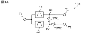
- FIG. 1A is a circuit block diagram of a filter device according to a first embodiment.
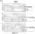
- FIG. 1B is a graph showing the pass characteristic of the filter device according to the first embodiment.
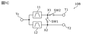
- FIG. 1C is a circuit block diagram of a filter device according to a first modification.
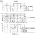
- FIG. 1D is a graph showing the pass characteristic of the filter device according to the first modification.
- FIG. 2A is a circuit block diagram of a filter device according to Comparative Example 1.
- FIG. 2B is a graph showing the pass characteristic of the filter device according to Comparative Example 1.
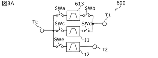
- FIG. 3A is a circuit block diagram of a filter device according to comparative example 2.
- FIG. 3B is a graph showing the pass characteristic of the filter device according to Comparative Example 2.
- FIG. 4A is a Smith chart for comparing the impedances on the common terminal side of the filter mode in Example 1 and Comparative Example 2.
- FIG. 4B is a Smith chart comparing the impedance on the input / output terminal side of the filter mode in the first embodiment and the second comparative example.
- FIG. 5A is a circuit block diagram of a filter device according to a second embodiment.
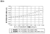
- FIG. 5B is a graph showing the relationship between the off capacitance and the insertion loss of the second switch element in the filter mode of the first embodiment and the second embodiment.
- FIG. 6A is a graph showing pass characteristics when the off capacitance of the first switch element of the filter device according to the second embodiment is changed.
- FIG. 6B is a graph showing the relationship between the off capacitance and the insertion loss of the first switch element in the duplexer mode of the first embodiment and the second embodiment.
- FIG. 6C is a graph showing the insertion loss when the off capacitance of the switch element is changed.
- FIG. 6D is a graph showing the insertion loss when the off capacitance of the circuit in which the shunt switch element in the conductive state is connected to the switch element is changed.
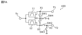
- FIG. 7A is a circuit block diagram of a filter device according to a third embodiment.
- FIG. 7B is a graph comparing the pass characteristics of the filter devices according to the second embodiment and the third embodiment.
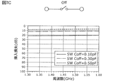
- FIG. 7C is a graph showing the insertion loss when the off capacitance of the switch element in the non-conductive state is changed.
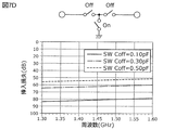
- FIG. 7D is a graph showing the insertion loss when the off capacitance of the circuit in which the shunt switch element in the conductive state is connected to the connection node of two switch elements connected in series is changed.
- FIG. 8 is a graph showing the pass characteristic, the amplitude characteristic, the phase characteristic, and the impedance characteristic of the filter device according to the third embodiment.
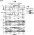
- FIG. 9A is a graph showing pass characteristics, phase difference characteristics, and impedance characteristics when the phase on the input / output terminal side in the filter mode of the third embodiment is changed.
- FIG. 9B is a graph showing the relationship between the maximum impedance frequency of the second filter and the inter-filter phase difference when the phase on the input / output terminal side is changed in the filter mode of the third embodiment, and the insertion loss and the ripple.
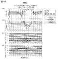
- FIG. 10A is a graph showing pass characteristics, phase difference characteristics, and impedance characteristics when the phase on the common terminal side in the filter mode in Example 3 is changed.
- FIG. 10B is a graph showing the relationship between the maximum impedance frequency of the second filter and the inter-filter phase difference when the phase on the common terminal side is changed in the filter mode of the third embodiment, and the insertion loss and the ripple.
- FIG. 10A is a graph showing pass characteristics, phase difference characteristics, and impedance characteristics when the phase on the common terminal side in the filter mode in Example 3 is changed.
- FIG. 10B is a graph showing the relationship between the maximum impedance frequency of the second filter and the inter-filter phase difference when the phase on the common terminal side is changed in the filter mode of the third embodiment, and the
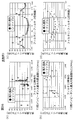
- FIG. 11A is a graph showing pass characteristics, phase difference characteristics, and impedance characteristics when the phases on the common terminal side and the input / output terminal side in the filter mode in Example 3 are changed.
- FIG. 11B shows the relationship between the maximum impedance frequency of the second filter and the inter-filter phase difference, and the insertion loss and ripple when the phases on the common terminal side and the input / output terminal side in the filter mode of Example 3 are changed. It is a graph.
- FIG. 12 is a specific circuit configuration diagram of the filter device according to the third embodiment.
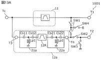
- FIG. 13A is a circuit configuration diagram of a filter device according to a second modification.
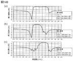
- FIG. 13B is a graph showing the pass characteristic of the filter device according to the second modification.
- FIG. 14A is a circuit configuration diagram of a filter device according to a third modification.
- FIG. 14B is a graph showing the pass characteristic of the filter device according to the third modification.
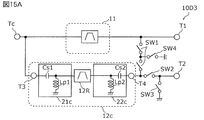
- FIG. 15A is a circuit configuration diagram of a filter device according to a fourth modification.
- FIG. 15B is a graph showing the pass characteristic of the filter device according to the fourth modification.
- FIG. 16A is a circuit configuration diagram of a filter device according to a fifth modification.
- FIG. 16B is a graph showing the pass characteristic of the filter device according to the fifth modification.
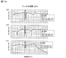
- FIG. 17A is a graph showing the broadband pass characteristic of the filter device according to the fifth modification.
- FIG. 17B is a graph showing the wide band pass characteristic of the filter device according to the second modification.
- FIG. 15A is a circuit configuration diagram of a filter device according to a fourth modification.
- FIG. 15B is a graph showing the pass characteristic of the filter device according to the fourth modification.
- FIG. 16A is a circuit configuration diagram of
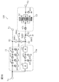
- FIG. 18 is a circuit diagram of a filter device according to a fourth embodiment.
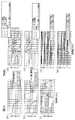
- FIG. 19 is a graph showing the pass characteristic, the amplitude characteristic, the phase characteristic, and the impedance characteristic of the filter device according to the fourth embodiment.
- FIG. 20 is a graph comparing the pass characteristics of the filter devices according to the third embodiment and the fourth embodiment.
- FIG. 21A is a circuit configuration diagram of a filter device according to a fifth embodiment.
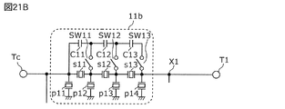
- FIG. 21B is a circuit configuration diagram showing a modification of the first filter according to the fifth embodiment.
- FIG. 22A is a graph showing the pass characteristic, the amplitude characteristic, the phase characteristic, and the impedance characteristic of the filter device according to the fifth embodiment.
- FIG. 22B is a graph showing the pass characteristics of the 1a band and the 2a band in the duplexer mode according to the fifth embodiment.
- FIG. 23A is a circuit configuration diagram of a sixth modified example of each filter that constitutes the filter device according to the fifth embodiment.
- FIG. 23B is a circuit configuration diagram of Modified Example 7 of each filter that constitutes the filter device according to Example 5.
- FIG. 23C is a circuit configuration diagram of Modified Example 8 of each filter constituting the filter device according to Example 5.
- FIG. 23D is a circuit configuration diagram of modification 9 of each filter constituting the filter device according to the fifth embodiment.
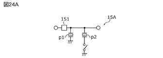
- FIG. 24A is a circuit configuration diagram of Modification Example 10 of each filter constituting the filter device according to the fifth embodiment.
- FIG. 24B is a circuit configuration diagram of Modification 11 of each filter that constitutes the filter device according to Embodiment 5.
- FIG. 24C is a circuit configuration diagram of modification 12 of each filter constituting the filter device according to the fifth embodiment.
- FIG. 24D is a circuit configuration diagram of modification 13 of each filter that constitutes the filter device according to the fifth embodiment.
- FIG. 24E is a circuit configuration diagram of modification 14 of each filter constituting the filter device according to the fifth embodiment.
- FIG. 24F is a circuit configuration diagram of modification 15 of each filter constituting the filter device according to the fifth embodiment.
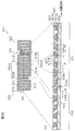
- FIG. 25 is a mounting configuration diagram of the filter device according to the fifth embodiment.
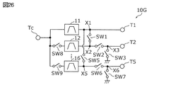
- FIG. 26 is a circuit diagram of a filter device according to a sixth embodiment.
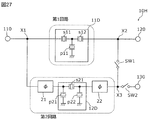
- FIG. 27 is a circuit diagram of a high frequency filter according to Embodiments 1a, 1b, 1c, 1d and 1e.
- FIG. 28 is an example of a diagram schematically illustrating the structure of a parallel arm resonator according to the first embodiment.
- FIG. 29A is a graph comparing the pass characteristic and the reflection characteristic of the high frequency filters according to Example 1a and Example 1e.
- FIG. 29B is a graph comparing impedance characteristics and reflection characteristics of series arm resonators according to Example 1a and Example 1e.
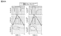
- FIG. 30A is a graph comparing the pass characteristics of the high frequency filters according to Example 1 b and Example 1 e.
- FIG. 30B is a graph comparing impedance characteristics and reflection characteristics of parallel arm resonators according to Example 1 b and Example 1 e.
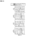
- FIG. 31A is a graph comparing the pass characteristics of the high frequency filters according to Example 1c and Example 1e.
- FIG. 31B is a graph comparing impedance characteristics and reflection characteristics of parallel arm resonators according to Example 1 c and Example 1 e.
- FIG. 32 is a graph comparing the pass characteristic and the reflection characteristic of the high frequency filters according to Example 1 d and Example 1 e.
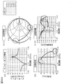
- FIG. 33A is a graph showing a change in characteristics when the IR pitch is changed at 0.40 ⁇ to 0.50 ⁇ in the resonator of the typical example.
- FIG. 34A is a configuration diagram of a communication device according to Embodiment 2.
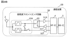
- FIG. 34B is a block diagram of a communication device according to a first modification of the second embodiment.
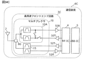
- FIG. 34C is a block diagram of a communication device according to a second modification of the second embodiment.
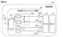
- FIG. 34D is a block diagram of a communication device according to a third modification of the second embodiment.
- the resonant frequency in the resonator or circuit is a resonant frequency for forming an attenuation pole in the pass band or near the pass band of the resonator or the filter including the circuit, and the resonator Alternatively, it is the frequency of the “resonance point” which is a singular point at which the impedance of the circuit becomes minimum (ideally, the point at which the impedance is 0).
- the antiresonance frequency in the resonator or the circuit is an antiresonance frequency for forming an attenuation pole in the pass band or near the pass band of the resonator or the filter including the circuit, unless otherwise specified. It is the frequency of the "anti-resonance point" which is a singular point at which the impedance of the resonator or the circuit concerned is maximal (ideally, the point at which the impedance is infinite).
- a series arm (resonance) circuit and a parallel arm (resonance) circuit are defined as follows.
- the parallel arm (resonance) circuit is a circuit disposed between one node on a path connecting the first input / output terminal and the second input / output terminal and the ground.
- the series arm (resonance) circuit is a circuit disposed between the first input / output terminal or the second input / output terminal and a node on the above path to which the parallel arm (resonance) circuit is connected, or The circuit is disposed between one node on the path to which the parallel arm (resonance) circuit is connected and the other node on the path to which the other parallel arm (resonance) circuit is connected.
- passband lower end means “the lowest frequency in the passband”.
- pass band high end means “the highest frequency in the pass band”.
- low pass band side means “outside of pass band and lower frequency side than pass band”.
- high pass side of pass band means “outside of pass band and higher frequency side than pass band”.
- the “low frequency side” may be referred to as the “low frequency side”
- the “high frequency side” may be referred to as the “high frequency side”.
- FIG. 1A is a circuit block diagram of a filter device 10A according to a first embodiment.
- the filter device 10A shown in the figure includes filters 11 and 12, switches SW1 and SW2, a common terminal Tc, and input / output terminals T1 and T2.
- the filter 11 is a first filter connected on a first path connecting the common terminal Tc and the input / output terminal T1 and having a first band as a pass band.
- the filter 12 is a second filter connected on a second path connecting the common terminal Tc and the input / output terminal T2 and having a second band as a pass band.
- the second band is a frequency band higher than the frequency of the first band and not overlapping the frequency of the first band.
- the input / output terminal T1 corresponds to a first input / output terminal
- the input / output terminal T2 corresponds to a second input / output terminal.
- the switch SW1 is a first switch element connected between the node X1 and the node X2.
- the switch SW2 is a second switch element connected between the node X2 and the input / output terminal T2.
- the node X1 is a first node on the first path between the filter 11 and the input / output terminal T1, and the node X2 is on the second path between the filter 12 and the input / output terminal T2. It is a second node.
- FIG. 1B is a graph showing the pass characteristic of the filter device 10A according to the first embodiment.
- the pass characteristic between the common terminal Tc and the input / output terminal T1 when the switch SW1 is turned on (on) and the switch SW2 is turned off (off) is shown in (a) of the figure.
- (b) of the same drawing shows the passage characteristic between the common terminal Tc and the input / output terminal T1 when the switch SW1 is turned off and the switch SW2 is turned on.
- (c) of the same drawing shows a passing characteristic between the common terminal Tc and the input / output terminal T2 when the switch SW1 is turned off and the switch SW2 is turned on.
- the first band of the filter 11 is a band (1428) including the transmission band (Band11Tx: 1428-1448 MHz) of Band 11 and the transmission band (Band 21 Tx: 1448-1463 MHz) of Band 21 in Long Term Evolution (LTE). -1463 MHz).
- the second band of the filter 12 is a band (1476-1511 MHz) including the band 11 reception band of Band 11 (Band 11 Rx: 1476-1496 MHz) and the reception band of Band 21 (Band 21 Rx: 1496-1511 MHz).
- the filter device 10A when the switch SW1 is turned on and the switch SW2 is turned off, the filter device 10A is configured to set the first band and the second band between the common terminal Tc and the input / output terminal T1.
- the third band is a band (1428-1511 MHz) including the band 32 reception band (Band 32 Rx: 1452-1496 MHz) of LTE. That is, the third band is a band including at least a part of the first band and at least a part of the second band.
- the second band is not defined as a band constituted by a plurality of discrete bands, but is defined as one band continuous in frequency.
- the filter device 10A is configured to connect the common terminal Tc to the input / output terminal T1.
- a duplexer (multiplexer) connected by the common terminal Tc is configured.
- the common terminal Tc and the input / output terminal (2) has a relatively narrow band pass band, which is the first band, and a filter 11 which passes between the common terminal Tc and the input / output terminal T1
- Multiplexer for multiplexing or demultiplexing signals and signals having a relatively narrow band pass band which is the second band and passing through the filter 12 formed between the common terminal Tc and the input / output terminal T2 It is possible to provide a compact filter device that switches between
- the common terminal Tc is used not only when the on and off of the switch SW1 and the switch SW2 are exclusively switched, but also when both the switch SW1 and the switch SW2 are on. Can be applied as a power divider (or a power combiner) between the input terminal and the input / output terminals T1 and T2. When both of the switch SW1 and the switch SW2 are off, it can be applied as a narrow band filter (filter 11) having a first band as a pass band between the common terminal Tc and the input / output terminal T1.
- the switch SW2 may be disposed between the node X1 and the input / output terminal T1 instead of being disposed between the node X2 and the input / output terminal T2.
- FIG. 1C is a circuit block diagram of a filter device 10B according to a first modification.
- the filter device 10B shown in the figure includes filters 11 and 12, switches SW1 and SW2, a common terminal Tc, and input / output terminals T1 and T2.
- the filter device 10B according to the present modification differs from the filter device 10A according to the first embodiment in the arrangement of the switch SW2.
- the filter device 10B according to the present modification will not be described the same as the filter device 10A according to the first embodiment, and different points will be mainly described.
- the filter 11 is a second filter connected on a second path connecting the common terminal Tc and the input / output terminal T1 (second input / output terminal), and using a second band as a pass band.
- the filter 12 is a first filter connected on a first path connecting the common terminal Tc and the input / output terminal T2 (first input / output terminal) and having a first band as a pass band.
- the second band is a frequency band lower than the frequency of the first band and not overlapping the frequency of the first band.
- the input / output terminal T1 corresponds to a second input / output terminal
- the input / output terminal T2 corresponds to a first input / output terminal.
- the switch SW1 is a first switch element connected between the node X1 and the node X2.
- the switch SW2 is a second switch element connected between the node X1 and the input / output terminal T1.
- the node X1 is a second node on the second path between the filter 11 and the input / output terminal T1, and the node X2 is on the first path between the filter 12 and the input / output terminal T2. It is a first node.
- FIG. 1D is a graph showing the pass characteristic of the filter device 10B according to the first modification.
- the pass characteristic between the common terminal Tc and the input / output terminal T2 when the switch SW1 is turned on and the switch SW2 is turned off is shown in FIG.
- (b) of the same drawing shows the passage characteristic between the common terminal Tc and the input / output terminal T1 when the switch SW1 is turned off and the switch SW2 is turned on.
- (c) of the same drawing shows a passing characteristic between the common terminal Tc and the input / output terminal T2 when the switch SW1 is turned off and the switch SW2 is turned on.
- the filter device 10B is configured to set the first band and the second band between the common terminal Tc and the input / output terminal T1. To form a filter having a relatively broad band third band.
- the filter device 10B when the switch SW1 is turned off and the switch SW2 is turned on, the filter device 10B generates the second filter between the common terminal Tc and the input / output terminal T1.
- a duplexer (multiplexer) connected by the common terminal Tc is configured.
- the common terminal Tc is used not only when the on and off of the switch SW1 and the switch SW2 are exclusively switched, but also when both the switch SW1 and the switch SW2 are on. Can be applied as a power divider (or a power combiner) between the input terminal and the input / output terminals T1 and T2. When both the switch SW1 and the switch SW2 are off, it can be applied as a narrow band filter (filter 12) having the first band as the pass band between the common terminal Tc and the input / output terminal T2.
- the position where the switch SW2 is connected may be on the filter 12 side or on the filter 11 side.
- the switch SW2 since the switch SW2 is connected between the filter 12 and the input / output terminal T2, the signal on the filter 11 side (between the common terminal Tc and the input / output terminal T1) in which the switch SW2 is not disposed Propagation loss is reduced.
- the switch SW2 since the switch SW2 is connected between the filter 11 and the input / output terminal T1, the signal on the filter 12 side (between the common terminal Tc and the input / output terminal T2) in which the switch SW2 is not disposed Propagation loss is reduced.
- the switch SW2 be connected to the terminal to which the low noise amplifier is connected. This is because the size of the switch having high power durability is increased, and the switch SW2 can be miniaturized by arranging the switch SW2 on the low power low noise amplifier side.
- the filter device 10A is used as a filter for time division duplex (TDD) between the common terminal Tc and the input / output terminal T1 when the switch SW1 is on and the switch SW2 is off. May be On the other hand, when the switch SW1 is off and the switch SW2 is on, the frequency division duplex (FDD) method is performed between the common terminal Tc and the input / output terminal T1 and between the common terminal Tc and the input / output terminal T2.
- TDD time division duplex
- a filter for TDD configured between the common terminal Tc and the input / output terminal T1 with the third band of wide band as the pass band
- a relatively narrow band which is the first band
- the filter device 10B when the switch SW1 is on and the switch SW2 is off, the filter device 10B according to the modification 1 is a filter for time division duplex (TDD) between the common terminal Tc and the input / output terminal T2. It may be used.
- TDD time division duplex
- FDD frequency division duplex
- a filter for TDD configured between the common terminal Tc and the input / output terminal T2 with the third band of wide band as the pass band, and (2) a relatively narrow band which is the first band And a signal passing through the filter 12 formed between the common terminal Tc and the input / output terminal T2, and a relatively narrow band pass band, which is the second band, It is possible to provide a compact filter device that doubles as a FDD multiplexer that combines or demultiplexes a signal that passes through the filter 11 configured between the input / output terminal T1 and the signal.
- the filter devices 10A and 10B according to the first embodiment and the first modification can realize a filter having a wide band pass band and a multiplexer having a plurality of narrow band pass bands with a small circuit configuration
- the configuration and characteristics of the filter device according to Example 1 and Comparative Example 2 will be described.
- FIG. 2A is a circuit block diagram of a filter device 500 according to Comparative Example 1.
- the filter device 500 shown in the figure includes filters 11, 12 and 512, switches SWa, SWb and SWc, a common terminal Tc, and input / output terminals T1 and T2.
- the filter 11 is a filter connected on a first path connecting the common terminal Tc and the input / output terminal T1 and using a first band as a pass band.
- the filter 12 is connected on a second path connecting the common terminal Tc and the input / output terminal T2, and is a filter that uses a second band as a pass band.
- the filter 512 is a filter connecting the common terminal Tc and the input / output terminal T1 on a fourth path different from the first path and setting the second band as a pass band.
- the second band is a frequency band higher than the frequency of the first band and not overlapping the frequency of the first band.
- the switch SWa is connected on a fourth path between the common terminal Tc and the filter 512
- the switch SWb is connected on a fourth path between the filter 512 and the input / output terminal T1
- the switch SWc is common
- the second path between the terminal Tc and the filter 12 is connected.
- FIG. 2B is a graph showing the pass characteristic of the filter device 500 according to the first comparative example.
- the pass characteristic between the common terminal Tc and the input / output terminal T1 when the switches SWa and SWb are turned on and the switch SWc is turned off is shown in FIG.
- (b) of the same drawing shows the passage characteristic between the common terminal Tc and the input / output terminal T1 when the switches SWa and SWb are turned off and the switch SWc is turned on.
- (c) of the same drawing shows the passage characteristic between the common terminal Tc and the input / output terminal T2 when the switches SWa and SWb are turned off and the switch SWc is turned on.
- the first band is a band including the transmission band of Band 11 of LTE and the transmission band of Band 21 and the second band is the reception band of Band 11 of LTE and Band 21.
- a band including a reception band is used, and a third band is a band including a reception band of Band 32 of LTE.
- the filter device 500 operates the filter 11 and the filter 512 between the common terminal Tc and the input / output terminal T1. And a filter having a relatively wide band third band including the first band and the second band.
- the filter device 500 operates between the common terminal Tc and the input / output terminal T1. And a filter 11 having a relatively narrow band pass band which is a first band, and a filter 12 having a relatively narrow band pass band which is a second band between the common terminal Tc and the input / output terminal T2. And constitute a duplexer (multiplexer) connected at the common terminal Tc.
- the filter device 500 according to Comparative Example 1 needs three filters 11, 12 and 512, and three switches SWa, SWb and SWc, so the size is smaller than that of the filter device 10A according to the first embodiment. Becomes larger.
- the insertion loss on the filter 11 side of the comparative example 1 is 3.75 dB, and the insertion loss on the filter 12 side is 3.56 dB.
- the insertion loss on the filter 11 side is 3.60 dB, and the insertion loss on the filter 12 side is 3.56 dB. That is, the insertion loss on the side of the filter 11 of Comparative Example 1 is larger than that of Example 1. This is because the number of switches added in series is larger in Comparative Example 1 and the switch loss in the multiplexer is larger.
- FIG. 3A is a circuit block diagram of a filter device 600 according to Comparative Example 2. As shown in FIG. The filter device 600 shown in the figure includes filters 11, 12 and 613, switches SWa, SWb, SWc, SWd and SWe, a common terminal Tc, and input / output terminals T1 and T2.
- the filter 11 is a filter connected on a first path connecting the common terminal Tc and the input / output terminal T1 and using a first band as a pass band.
- the filter 12 is connected on a second path connecting the common terminal Tc and the input / output terminal T2, and is a filter that uses a second band as a pass band.
- the filter 613 is a filter connecting the common terminal Tc and the input / output terminal T1 on a fourth route different from the first route and setting the third band as a pass band.
- the second band is a frequency band higher than the frequency of the first band and not overlapping the frequency of the first band.
- the third band is a relatively wide band of frequency including the first band and the second band.
- the switch SWa is connected on a fourth path between the common terminal Tc and the filter 613, the switch SWb is connected on a fourth path between the filter 613 and the input / output terminal T1, and the switch SWc is common
- the switch SWd is connected on the first path between the terminal Tc and the filter 11, the switch SWd is connected on the first path between the filter 11 and the input / output terminal T1, and the switch SWe is connected to the common terminal Tc and the filter 12 And a second path between them.
- FIG. 3B is a graph showing the pass characteristic of the filter device 600 according to the second comparative example.
- the pass characteristic between the common terminal Tc and the input / output terminal T1 when the switches SWa and SWb are turned on and the switches SWc, SWd and SWe are turned off is shown in FIG.
- (b) of the same drawing shows the passage characteristic between the common terminal Tc and the input / output terminal T1 when the switches SWa and SWb are turned off and the switches SWc, SWd and SWe are turned on.
- (c) of the same drawing shows the passage characteristic between the common terminal Tc and the input / output terminal T2 when the switches SWa and SWb are turned off and the switches SWc, SWd and SWe are turned on.
- the first band is a band including the transmission band of Band 11 of LTE and the transmission band of Band 21 and the second band is the reception band of Band 11 of LTE and Band 21.
- a band including a reception band is used, and a third band is a band including a reception band of Band 32 of LTE.
- the filter device 600 performs filtering between the common terminal Tc and the input / output terminal T1.
- a filter having a relatively wide third band including the first band and the second band is configured.
- the filter device 600 when the switches SWa and SWb are turned off and the switches SWc, SWd and SWe are turned on, the filter device 600 includes the common terminal Tc and the input / output terminal T1. Between the common terminal Tc and the input / output terminal T2, the relatively narrow band pass band being the second band, and the filter 11 having the relatively narrow band pass band being the first band. And a filter 12 having a pair of terminals, to constitute a duplexer (multiplexer) connected at a common terminal Tc.
- the filter device 600 according to the comparative example 2 requires the three filters 11, 12 and 613 and the five switches SWa, SWb, SWc, SWd and SWe, the filter device 10A according to the first embodiment and Compared to the size is larger.
- FIG. 4A is a Smith chart comparing the impedance on the common terminal Tc side in the filter mode of Example 1 and Comparative Example 2.
- FIG. 4B is a Smith chart for comparing the impedance on the input / output terminal T1 side in the filter mode of the first embodiment and the second comparative example.
- the impedance on the common terminal Tc side is Is represented.
- the impedance of is represented.
- the “filter mode” in the present embodiment is switched to a filter having the third band as a pass band between the common terminal Tc and the input / output terminal T1 (in the first modification, the input / output terminal T2). Show the condition.
- a filter having a relatively narrow band pass band which is a first band between the common terminal Tc and the input / output terminal T1, and between the common terminal Tc and the input / output terminal T2
- a filter having a relatively narrow pass band, which is the second band is switched to the duplexer connected at the common terminal Tc.
- the filter characteristic having the third band, which is a wide band, as the pass band is configured by one filter 613.
- the concentration of impedance on the input side and output side in the passband is both poor. Therefore, there is a problem that a good impedance matching with an amplifier connected to the front stage or the rear stage of the filter device 600 can not be obtained. For example, if the amplifier is a low noise amplifier, there is a problem that the noise figure (NF) becomes worse.
- NF noise figure
- the filter device 10A according to the first embodiment and the filter device 10B according to the first modification compared with the filter device 500 according to the comparative example 1 and the filter device 600 according to the comparative example 2, two filter elements and two switches
- the element can realize a filter having a relatively wide band passband and a duplexer (multiplexer) having a plurality of relatively narrow band passbands. Therefore, it is possible to provide a low loss and compact filter device.
- FIG. 5A is a circuit block diagram of a filter device 10C according to a second embodiment.
- the filter device 10C shown in the figure includes filters 11 and 12, switches SW1, SW2 and SW3, a common terminal Tc and input / output terminals T1 and T2.
- the filter device 10C according to the present embodiment differs from the filter device 10A according to the first embodiment in that a switch SW3 is added.
- the filter device 10C according to the present embodiment will not be described the same as the filter device 10A according to the first embodiment, and differences will be mainly described.
- the switch SW1 is a first switch element connected between the node X1 and the node X2.
- the switch SW2 is a second switch element connected between the node X2 and the input / output terminal T2.
- the switch SW3 is a third switch element connected between the node X3 and the ground.
- the node X1 is a first node on the first path between the filter 11 and the input / output terminal T1
- the node X2 is on the second path between the filter 12 and the input / output terminal T2. It is a second node.
- the node X3 is a third node on the second path and between the switch SW2 and the input / output terminal T2.
- the switch SW2 and the switch SW3 are exclusively switched on and off.
- FIG. 5B is a graph showing the relationship between the off capacitance and the insertion loss of the switch SW2 in the filter mode of the first embodiment and the second embodiment.
- the off capacitance refers to the capacitance component of the switch when the switch is in the off state.
- the filter device 10A according to the first embodiment is applied as a wide band filter having the third band as the pass band, the switch SW2 is off, but the off capacitance of the switch SW2 is large.
- the insertion loss of the 3rd zone is increasing. This is because the amount of signal leakage to the unused input / output terminal T2 increases as the off capacitance of the switch SW2 increases.
- the filter device 10B according to the second embodiment when the filter device 10B according to the second embodiment is applied as a wide band filter having the third band as the pass band, the insertion loss of the third band increases as the off capacity of the switch SW2 increases.
- the increase rate of insertion loss in the third band is reduced. This is because when the switch SW2 is off, the switch SW3 is turned on and the node X3 is shunted to the ground, thereby improving the isolation from the switch SW2 to the input / output terminal T2, and to the unused input / output terminal T2. This is because signal leakage is suppressed.
- the passband of the filter having the third band as the passband which is formed between the common terminal Tc and the input / output terminal T1. Insertion loss can be reduced.
- the off capacitance Coff of the switch SW2 0.35 pF or less.
- the deterioration of the insertion loss with respect to the ideal switch element can be 0.1 dB or less.
- the third wide band is set as the pass band, and between the common terminal Tc and the input / output terminal T1.
- the insertion loss of the configured filter can be reduced.
- FIG. 6A is a graph showing the passage characteristic when the off capacitance of the switch SW1 of the filter device 10C according to the second embodiment is changed. More specifically, in (a) of FIG. 6A, the common terminal when the off capacitance of the switch SW1 is changed when the switch SW1 of the filter device 10C according to the second embodiment is off and the switch SW2 is on. A pass characteristic between the Tc and the input / output terminal T1 is shown. Further, in (b) of FIG. 6A, the common terminal Tc—input / output when the off capacitance of the switch SW1 is changed when the switch SW1 of the filter device 10C according to the second embodiment is off and the switch SW2 is on. Passage characteristics between the terminals T2 are shown.
- FIG. 6B is a graph showing the relationship between the off-capacitance of the switch SW1 and the insertion loss in the duplexer modes of the first embodiment and the second embodiment.
- the first band (Band 11 Tx and Band 21 Tx) between the common terminal Tc and the input / output terminal T1 when the switch SW1 is off and the switch SW2 is on in the first embodiment and the second embodiment is illustrated in (a) of FIG. Insertion loss and attenuation of the second band (Band 11 Rx and Band 21 Rx) are shown.
- the attenuation characteristics in the vicinity of the pass band of the multiplexer deteriorate.
- the off-capacitance of the switch SW1 is larger, along with the deterioration of the attenuation characteristics near the pass band of the multiplexer, the insertion loss of the pass band is also worse.
- the amount of attenuation required for the multiplexer is approximately 20 dB or more, it is desirable that the off capacitance Coff of the switch SW1 be 0.1 dB or less.
- FIG. 6C is a graph showing isolation (attenuation amount) between the switches SW1 when the off capacitance of the switch SW1 in the filter device 10C according to the second embodiment is changed. Further, FIG. 6D shows the isolation (attenuation amount) between the switch circuits when the off capacitance of the switch SW2 is changed in the switch circuit configured by the switches SW2 and SW3 in the filter device 10C according to the second embodiment. It is a graph.
- the switch SW1 when configuring the multiplexer, the switch SW1 is turned off. Therefore, when the off capacitance Coff of the switch SW1 is large, the characteristics of the filters 11 and 12 affect each other, and the attenuation characteristics are deteriorated at the frequencies of the respective passbands.
- the switch SW2 side is turned off when configuring a filter that uses the third band of wide band as the pass band, but there is no device that allows the signal to pass through at the input / output terminal T2 side of the filter 12, so the off capacitance Even if Coff increases, it does not affect the amount of attenuation.
- the passband signal leaks, the insertion loss in the passband is aggravated.
- isolation can be improved by the switch SW3.
- FIG. 7A is a circuit block diagram of a filter device 10D according to a third embodiment.
- the filter device 10D shown in the figure includes filters 11 and 12, switches SW1, SW2, SW3 and SW4, a common terminal Tc, and input / output terminals T1 and T2.
- the filter device 10D according to the present embodiment differs from the filter device 10C according to the second embodiment in that the switch SW1 is divided in series and the switch SW4 is added.
- the filter device 10D according to the present embodiment will not be described the same as the filter device 10C according to the second embodiment, and differences will be mainly described.
- the switch SW1 is a first switch element connected between the node X1 and the node X2.
- the switch SW1 is composed of a plurality of unit switches connected in series.
- the switch SW4 is connected between the ground and a node X4 (fourth node) which is any connection node of a plurality of unit switches connected in series, and is turned on and off exclusively with the switch SW1. It is a four switch element.
- the switch SW1 is composed of a plurality of unit switches connected in series with one another, for example, assuming that the stack number of the switch SW1 is n (n is an integer of 2 or more), the switch SW1 has a stack number k (k k is a natural number less than or equal to n ⁇ 1) and the number of stack circuits (n ⁇ k). Therefore, the size of the switch SW1 does not increase by dividing the switch SW1 into two series-divided switch circuits.
- the unit switch is, for example, a field effect transistor (FET).
- the switch SW1 and the switch SW4 are exclusively switched on and off.
- FIG. 7B is a graph comparing the pass characteristics of the filter devices according to the second embodiment and the third embodiment.
- (A) to (c) of FIG. 7B are graphs comparing the pass characteristics of Example 2 and Example 3 when the off capacitance of the switch SW1 is 0.05 pF.
- (d) to (e) of FIG. 7B are graphs comparing the pass characteristics of the filter mode of the second embodiment and the third embodiment when the off capacitance of the switch SW1 is 0.50 pF.
- FIG. 7C is a graph showing isolation (attenuation amount) between the switches SW1 when the off capacitance of the switch SW1 in the filter device 10C according to the second embodiment is changed.
- 7D shows isolation between switch circuits when the off capacitance of the switch SW1 is changed in the switch circuit configured by the switch SW1 and the switch SW4 which are divided in series in the filter device 10D according to the third embodiment.
- (Attenuation amount) is a graph.
- the switch SW1 when configuring the multiplexer, the switch SW1 is turned off. Therefore, when the off capacitance Coff of the switch SW1 is large, the signal leakage amount of the switch SW1 in the off state is increased (the insertion loss is reduced in FIG. 7C).
- the filter device 10D according to the third embodiment by arranging the switch SW4, as shown in FIG. 7D, even when the off capacitance Coff of the switch SW1 is large, the switch SW1 of the off state is The amount of signal leakage is reduced (the isolation is increased in FIG. 7D).
- the isolation between the filter 11 and the filter 12 is improved when the switch SW1 is in the OFF state, compared to the filter device 10C according to the second embodiment. Damping characteristics are improved. 7C and 7D, in the filter device 10D to which the switch SW4 is added, a sufficient amount of attenuation can be secured even if the off capacitance of the switch SW1 is large, so a small switch element having a large off capacitance ( It is possible to use a switch element having a small number of stacks.
- FIG. 8 is a graph showing the pass characteristic, the amplitude characteristic, the phase characteristic and the impedance characteristic of the filter device 10D according to the third embodiment.
- FIG. 8A shows the pass characteristic in the filter mode of the filter device 10D.
- the pass characteristics in the multiplexer mode of the filter device 10D are shown in (b) and (c) of FIG.
- FIG. 8 (d) shows the amplitude characteristics of the filter 11 alone and the filter 12 alone, and the difference in amplitude between them.
- FIG. 8E shows the phase characteristics of the filter 11 alone and the filter 12 alone, and the phase difference between them.
- unit from the common terminal Tc is shown by (f) of FIG. (G) of FIG. 8 shows impedance characteristics when looking at the filter 11 alone from the input / output terminal T1 and impedance characteristics when looking at the filter 12 alone from the input / output terminal T2.
- impedance refers to the impedance of reflection
- phase refers to the phase of passage
- the ripple (insertion loss deviation in the pass band) of the wide band filter having the third band as the pass band is improved. It becomes possible.
- Table 1 shows the insertion loss in the third band when the impedance on the common terminal T2 side of the filter 12 is fixed and the impedance on the input / output terminal T2 side is changed in the filter mode of the filter device 10D according to the third embodiment.
- the frequency difference between the filters 11 and 12 is 0 dB
- the phase difference between the filters 11 and 12 is 0 dB
- the frequency fz 21 at which the impedance on the common terminal Tc side of the filter 12 is maximum
- the maximum frequency fz 21 is shown.
- the phase of the first phase shifter and the phase of the second phase shifter shown in Table 1 are respectively the phase of the first phase shifter that the filter 12 has on the common terminal Tc side, and the phase of the filter 12.
- the phase of the second phase shifter provided on the input / output terminal T2 side is shown, and the filter 12 includes the first phase shifter, the second phase shifter, the first phase shifter, and the second phase shifter.
- FIG. 9A shows the pass characteristics and phase difference when the impedance on the common terminal Tc side of the filter 12 is fixed and the impedance on the input / output terminal T2 side is changed in the filter mode of the filter device 10D according to the third embodiment. It is a graph showing a characteristic and an impedance characteristic.
- FIG. 9B is a graph showing insertion loss and ripple in the third band when the phase on the input / output terminal T2 side of the filter 12 in the filter mode of the filter device 10D according to the third embodiment is changed.
- (A) of FIG. 9B is a graph showing the relationship between the impedance maximum frequency of the filter 12 and the insertion loss and ripple in the third band
- (b) of FIG. 9B enlarges the graph of (a) of FIG. 9B.
- (c) of FIG. 9B is a graph showing the relationship between the phase difference between the filters 11 and 12 and the insertion loss and ripple in the third band
- (d) of FIG. 9B is a graph of (c) of FIG. It is an enlarged graph.
- the impedance maximum frequency fz21 on the common terminal Tc side of the filter 12 and the impedance maximum frequency fz22 on the input / output terminal T2 side are at the second band low band end It can be seen that by being below the frequency, it is possible to reduce the large ripple exceeding 20 dB in the pass band of the wide band filter having the third band as the pass band to 20 dB or less.
- the phase difference between the filter 11 and the filter 12 is ⁇ 50 ° or more and + 50 ° or less, whereby the third band is a passband It can be seen that the large ripple exceeding 10 dB in the pass band of the wide band filter can be reduced to 10 dB or less.
- the impedance maximum frequency fz21 on the common terminal Tc side of the filter 12 alone and the impedance maximum frequency fz22 on the input / output terminal T2 side are the first band high. It can be seen that, by being equal to or lower than the frequency of the band edge, it is possible to reduce the large ripple exceeding 5 dB in the pass band of the wide band filter having the third band as the pass band to 5 dB or less.
- Table 2 shows the insertion loss in the third band when the impedance on the common terminal Tc side is changed by fixing the impedance on the input / output terminal T2 side of the filter 12 in the filter mode of the filter device 10D according to the third embodiment.
- the frequency difference between the filters 11 and 12 is 0 dB
- the phase difference between the filters 11 and 12 is 0 dB
- the frequency fz 21 at which the impedance on the common terminal Tc side of the filter 12 is maximum
- the maximum frequency fz 21 is shown.
- the phase of the first phase shifter and the phase of the second phase shifter shown in Table 2 are respectively the phase of the first phase shifter that the filter 12 has on the common terminal Tc side, and the phase of the filter 12.
- the phase of the second phase shifter provided on the input / output terminal T2 side is shown, and the filter 12 includes the first phase shifter, the second phase shifter, the first phase shifter, and the second phase shifter.
- FIG. 10A shows the pass characteristics and phase difference when the impedance on the input / output terminal T2 side of the filter 12 is fixed and the impedance on the common terminal Tc side is changed in the filter mode of the filter device 10D according to the third embodiment. It is a graph showing a characteristic and an impedance characteristic.
- FIG. 10B is a graph showing insertion loss and ripple in the third band when the phase on the common terminal Tc side of the filter 12 in the filter mode of the filter device 10D according to the third embodiment is changed.
- FIG. 10B (a) is a graph showing the relationship between the impedance maximum frequency of the filter 12 and the insertion loss and ripple in the third band
- FIG. 10B (b) enlarges the graph of FIG. 10B (a)
- FIG. 10B (c) is a graph showing the relationship between the phase difference between the filters 11 and 12 and the insertion loss and ripple in the third band
- FIG. 10B (d) is the graph of FIG. 10B (c). It is an enlarged graph.
- the impedance maximum frequency fz21 at the common terminal Tc side of the filter 12 and the impedance maximum frequency fz22 at the input / output terminal T2 are at the second band low band end It can be seen that by being below the frequency, it is possible to reduce the large ripple exceeding 20 dB in the pass band of the wide band filter having the third band as the pass band to 20 dB or less.
- the phase difference between the filter 11 and the filter 12 is ⁇ 50 ° or more and + 50 ° or less, whereby the third band is a passband It can be seen that the large ripple exceeding 10 dB in the pass band of the wide band filter can be reduced to 10 dB or less.
- the impedance maximum frequency fz21 on the common terminal Tc side of the filter 12 alone and the impedance maximum frequency fz22 on the input / output terminal T2 side are the first band high. It can be seen that, by being equal to or lower than the frequency of the band edge, it is possible to reduce the large ripple exceeding 5 dB in the pass band of the wide band filter having the third band as the pass band to 5 dB or less.
- Table 3 shows the insertion loss, ripple, and filter 11 in the third band when the impedances on the common terminal Tc side and the input / output terminal T2 side of the filter 12 are changed in the filter mode of the filter device 10D according to the third embodiment.
- the frequency difference between the 12 is 0 dB
- the phase difference between the filters 11 and 12 the frequency fz 21 at which the impedance on the common terminal Tc side of the filter 12 is maximum
- the phase of the first phase shifter and the phase of the second phase shifter shown in Table 3 are respectively the phase of the first phase shifter that the filter 12 has on the common terminal Tc side, and the phase of the filter 12.
- the phase of the second phase shifter provided on the input / output terminal T2 side is shown, and the filter 12 includes the first phase shifter, the second phase shifter, the first phase shifter, and the second phase shifter.
- 11A shows, in the filter mode of the filter device 10D according to the third embodiment, the pass characteristics, phase difference characteristics, and impedance characteristics when the impedances on the common terminal Tc side and the input / output terminal T2 side of the filter 12 are changed. It is a graph to represent.
- FIG. 11B is a graph showing insertion loss and ripple in the third band when the phases on the common terminal Tc side and the input / output terminal T2 side of the filter 12 in the filter mode of the filter device 10D according to the third embodiment are changed. It is. (A) of FIG. 11B is a graph showing the relationship between the impedance maximum frequency fz 21 on the common terminal Tc side of the filter 12 and the insertion loss and ripple in the third band, and (b) of FIG. The graph of a) is enlarged. FIG. 11B (c) is a graph showing the relationship between the impedance maximum frequency fz 22 on the input / output terminal T2 side of the filter 12 and the insertion loss and ripple in the third band, and FIG.
- FIG. 11B (d) is a diagram It is what expanded the graph of (c) of 11 B.
- FIG. 11B (e) is a graph showing the relationship between the phase difference between the filters 11 and 12 and the insertion loss and ripple in the third band
- FIG. 11B (f) is the graph of FIG. 11B (e). It is an enlarged graph.
- the impedance maximum frequency fz21 on the common terminal Tc side of the filter 12 and the impedance maximum frequency fz22 on the input / output terminal T2 side are the second band low band ends It can be seen that by setting the frequency equal to or lower than the above, it is possible to reduce the large ripple exceeding 20 dB in the pass band of the wide band filter having the third band as the pass band to 20 dB or less.
- the phase difference between the filter 11 and the filter 12 is ⁇ 50 ° or more and + 50 ° or less, whereby the third band is a passband It can be seen that the large ripple exceeding 10 dB in the pass band of the wide band filter can be reduced to 10 dB or less.
- the impedance maximum frequency fz21 on the common terminal Tc side of the filter 12 and the impedance maximum frequency fz22 on the input / output terminal T2 It can be seen that, by being below the frequency at the end, large ripples exceeding 5 dB in the pass band of the wide band filter having the third band as the pass band can be reduced to 5 dB or less.
- the filter 11 is a second filter connected on a second path connecting the common terminal Tc and the input / output terminal T1 (second input / output terminal) and having a second band as a pass band.
- the filter 12 is a first filter connected on a first path connecting the common terminal Tc and the input / output terminal T2 (first input / output terminal) and having a first band as a pass band.
- the second band is a frequency band lower than the frequency of the first band and not overlapping the frequency of the first band.
- the input / output terminal T1 corresponds to a second input / output terminal, and the input / output terminal T2 corresponds to a first input / output terminal.
- the filter 12 (first filter) is composed of a first phase shifter, a filter circuit, and a second phase shifter.
- the impedance maximum frequency fz21 on the common terminal Tc side of the filter 12 and the impedance maximum frequency fz22 on the input / output terminal T2 side are equal to or lower than the frequency of the first band low band end, thereby passing the third band
- the large ripple exceeding 20 dB in the pass band of the wide band filter can be reduced to 20 dB or less.
- the impedance maximum frequency fz21 on the common terminal Tc side of the filter 12 and the impedance maximum frequency fz22 on the input / output terminal T2 side are equal to or lower than the frequency of the second band high band end, thereby making the third band the pass band.
- the large ripple exceeding 5 dB in the pass band in the filter of can be reduced to 5 dB or less.
- FIG. 12 is a specific circuit configuration diagram of a filter device 10D according to the third embodiment.
- the filter 11 includes series arm resonators s11, s12 and s13 disposed on a path connecting the common terminal Tc and the node X1, and between each node on the path connecting the common terminal Tc and the node X1 and the ground.
- the parallel arm resonators p11, p12, p13 and p14 arranged are provided. With the above configuration, the filter 11 constitutes a ladder type band pass filter having the first band as the pass band.
- the filter 12 includes series arm resonators s21, s22 and s23 disposed on a second path connecting the common terminal Tc and the node X2, and a parallel arm disposed between each node on the second path and the ground.
- Resonators p21, p22, p23 and p24, phase shifters 21 and 22, and input / output terminals T3 and T4 are provided.
- the series arm resonators s21 to s23 and the parallel arm resonators p21 to p24 constitute a filter unit 12R having resonance characteristics.
- the phase shifter 21 is a first phase shifter connected between one terminal of the filter unit 12R and the input / output terminal T3 (third input / output terminal), and the phase shifter 22 is a component of the filter unit 12R. It is a second phase shifter connected between the other terminal and the input / output terminal T4 (fourth input / output terminal).
- the phase shifters 21 and 22 are composed of delay lines composed of distributed constant lines or lumped elements. According to the above configuration, the filter 12 constitutes a ladder type band pass filter whose phase can be adjusted, with the second band as the pass band.
- Table 4 shows an example of circuit parameters of the filter device 10D according to the third embodiment.
- FIG. 13A is a circuit configuration diagram of a filter device 10D1 according to the second modification.
- the filter device 10D1 shown in the figure shows a specific circuit configuration of the phase shifters 21 and 22 of the filter device 10D.
- the filter device 10D1 according to the present modification includes filters 11 and 12a, switches SW1 to SW4, a common terminal Tc, and input / output terminals T1 and T2.
- the filter 12a has a filter unit 12R, phase shifters 21a and 22a, and input / output terminals T3 and T4.
- phase shifters 21a and 22a have impedance elements composed of capacitors or inductors.
- phase shifter 21a has capacitors Cs11 and Cs12 arranged on the second path, and inductor Lp1 connected between the connection node of capacitors Cs11 and Cs12 and the ground.
- the phase shifter 22a also includes capacitors Cs21 and Cs22 arranged on the second path, and an inductor Lp2 connected between the connection node of the capacitors Cs21 and Cs22 and the ground. That is, each of the phase shifters 21a and 22a according to the present modification has a (T-type third-order) high-pass filter type circuit configuration.
- the phases of the phase shifters 21 and 22 are both positive values (phase on the + side), so the high-pass filter type circuit configuration Is suitable.
- FIG. 13B is a graph showing the pass characteristic of the filter device 10D1 according to the second modification.
- the pass characteristic between the common terminal Tc and the input / output terminal T1 when the switches SW1 and SW3 are turned on and the switches SW2 and SW4 are turned off is shown in FIG.
- (b) of the same drawing shows the pass characteristic between the common terminal Tc and the input / output terminal T1 when the switches SW1 and SW3 are turned off and the switches SW2 and SW4 are turned on.
- (c) of the same drawing shows the passage characteristic between the common terminal Tc and the input / output terminal T2 when the switches SW1 and SW3 are turned off and the switches SW2 and SW4 are turned on.
- the first band of the filter 11 is a band including the transmission band of Band 11 of LTE and the transmission band of Band 21.
- the second band of the filter 12a is a band including the reception band of Band 11 of LTE and the reception band of Band 21.
- the third band including at least a portion of the first band and at least a portion of the second band is a band including the reception band of Band 32 of LTE.
- the filter device 10D1 operates in the first band between the common terminal Tc and the input / output terminal T1. And a second wide band third band including the second band.
- the phases of the phase shifters 21a and 22a to values shown in Table 4, it is possible to optimize the phase difference between the filter 11 and the filter 12a.
- a lumped constant element such as a capacitor and an inductor, it is possible to optimize the phase difference between the filter 11 and the filter 12a, and it is possible to miniaturize the phase shifters 21a and 22a.
- the ripple of the filter having the relatively wide band third band including the first band and the second band is 4.15 dB, and it can be seen that low loss and low ripple in the third band are realized.
- FIG. 14A is a circuit configuration diagram of a filter device 10D2 according to the third modification.
- the filter device 10D2 shown in the figure shows a specific circuit configuration of the phase shifters 21 and 22 of the filter device 10D.
- a filter device 10D2 according to the present modification includes filters 11 and 12b, switches SW1 to SW4, a common terminal Tc, and input / output terminals T1 and T2.
- the filter 12b includes a filter unit 12R, phase shifters 21b and 22b, and input / output terminals T3 and T4.
- phase shifters 21b and 22b have impedance elements configured of capacitors or inductors.
- phase shifter 21b includes capacitor Cs1 arranged on the second path, and inductor Lp1 connected between the connection node of capacitor Cs1 and input / output terminal T3 and the ground.
- the phase shifter 22a further includes a capacitor Cs2 arranged on the second path, and an inductor Lp2 connected between the connection node of the capacitor Cs2 and the input / output terminal T4 and the ground. That is, each of the phase shifters 21b and 22b according to this modification has a (T-type second-order) high-pass filter type circuit configuration.
- the phases of the phase shifters 21 and 22 are both positive values (phase on the + side), so the high-pass filter type circuit configuration Is suitable.
- FIG. 14B is a graph showing the pass characteristic of the filter device 10D2 according to the third modification.
- the pass characteristic between the common terminal Tc and the input / output terminal T1 when the switches SW1 and SW3 are turned on and the switches SW2 and SW4 are turned off is shown in FIG.
- (b) of the same drawing shows the pass characteristic between the common terminal Tc and the input / output terminal T1 when the switches SW1 and SW3 are turned off and the switches SW2 and SW4 are turned on.
- (c) of the same drawing shows the passage characteristic between the common terminal Tc and the input / output terminal T2 when the switches SW1 and SW3 are turned off and the switches SW2 and SW4 are turned on.
- the filter device 10D2 sets the first band between the common terminal Tc and the input / output terminal T1. And a second wide band third band including the second band.
- the phases of the phase shifters 21 b and 22 b to the values shown in Table 4, it is possible to optimize the phase difference between the filter 11 and the filter 12.
- a lumped element such as a capacitor and an inductor, it is possible to optimize the phase difference between the filter 11 and the filter 12b, and the phase shifter 21b and the phase shifter 22b can be miniaturized.
- the ripple of the filter having the relatively wide band third band including the first band and the second band is 5.32 dB, and it can be seen that low loss and low ripple in the third band are realized.
- FIG. 15A is a circuit configuration diagram of a filter device 10D3 according to the fourth modification.
- the filter device 10D3 shown in the figure shows a specific circuit configuration of the phase shifters 21 and 22 of the filter device 10D.
- a filter device 10D3 according to the present modification includes filters 11 and 12c, switches SW1 to SW4, a common terminal Tc, and input / output terminals T1 and T2.
- the filter 12c has a filter unit 12R, phase shifters 21c and 22c, and input / output terminals T3 and T4.
- phase shifters 21c and 22c have impedance elements composed of capacitors or inductors. Specifically, phase shifter 21c has capacitor Cs1 arranged on the second path, and inductor Lp1 connected between the connection node of capacitor Cs1 and filter unit 12R and the ground. .
- the phase shifter 22c further includes a capacitor Cs2 arranged on the second path, and an inductor Lp2 connected between the connection node of the capacitor Cs2 and the filter unit 12R and the ground. That is, the phase shifters 21c and 22c according to this modification each have a (T-type second-order) high-pass filter type circuit configuration.
- the phases of the phase shifters 21 and 22 are both positive values (phase on the + side), so the high-pass filter type circuit configuration Is suitable.
- FIG. 15B is a graph showing the pass characteristic of the filter device 10D3 according to the fourth modification.
- the pass characteristic between the common terminal Tc and the input / output terminal T1 when the switches SW1 and SW3 are turned on and the switches SW2 and SW4 are turned off is shown in FIG.
- (b) of the same drawing shows the pass characteristic between the common terminal Tc and the input / output terminal T1 when the switches SW1 and SW3 are turned off and the switches SW2 and SW4 are turned on.
- (c) of the same drawing shows the passage characteristic between the common terminal Tc and the input / output terminal T2 when the switches SW1 and SW3 are turned off and the switches SW2 and SW4 are turned on.
- the filter device 10D3 operates in the first band between the common terminal Tc and the input / output terminal T1. And a second wide band third band including the second band.
- the phases of the phase shifters 21c and 22c to the values shown in Table 4, it is possible to optimize the phase difference between the filter 11 and the filter 12.
- a lumped constant element such as a capacitor and an inductor, it is possible to optimize the phase difference between the filter 11 and the filter 12c, and the phase shifters 21c and 22c can be miniaturized.
- the ripple of the filter having the relatively wide band third band including the first band and the second band is 5.05 dB, and it can be seen that low loss and low ripple in the third band are realized.
- FIG. 16A is a circuit configuration diagram of a filter device 10D4 according to the fifth modification.
- the filter device 10D4 shown in the figure shows a specific circuit configuration of the phase shifters 21 and 22 of the filter device 10D.
- the filter device 10D4 according to the present modification includes filters 11 and 12d, switches SW1 to SW4, a common terminal Tc, and input / output terminals T1 and T2.
- the filter 12d includes a filter unit 12R, phase shifters 21d and 22d, and input / output terminals T3 and T4.
- phase shifters 21 d and 22 d have impedance elements configured of capacitors or inductors.
- phase shifter 21d has inductors Ls11 and Ls12 arranged on the second path, and capacitor Cp1 connected between the connection node of inductors Ls11 and Ls12 and the ground.
- the phase shifter 22d also includes inductors Ls21 and Ls22 arranged on the second path, and a capacitor Cp2 connected between the connection node of the inductors Ls21 and Ls22 and the ground. That is, each of the phase shifters 21d and 22d according to the present modification has a (T-type third-order) low pass filter type circuit configuration.
- phase shifters 21 and 22 both have positive values (the phase on the + side), but the low frequency band as in this modification Even in the pass filter type circuit configuration, phase adjustment is possible.
- a phase shifter having a low-pass filter type circuit configuration is suitable for adjustment to a negative value (phase on the negative side).
- FIG. 16B is a graph showing the pass characteristic of the filter device 10D4 according to the fifth modification.
- the pass characteristic between the common terminal Tc and the input / output terminal T1 when the switches SW1 and SW3 are turned on and the switches SW2 and SW4 are turned off is shown in FIG.
- (b) of the same drawing shows the pass characteristic between the common terminal Tc and the input / output terminal T1 when the switches SW1 and SW3 are turned off and the switches SW2 and SW4 are turned on.
- (c) of the same drawing shows the passage characteristic between the common terminal Tc and the input / output terminal T2 when the switches SW1 and SW3 are turned off and the switches SW2 and SW4 are turned on.
- the filter device 10D4 sets the first band between the common terminal Tc and the input / output terminal T1. And a second wide band third band including the second band.
- the phases of the phase shifters 21 d and 22 d to values shown in Table 4, it is possible to optimize the phase difference between the filter 11 and the filter 12.
- a lumped constant element such as a capacitor and an inductor, it is possible to optimize the phase difference between the filter 11 and the filter 12d, and the phase shifters 21d and 22d can be miniaturized.
- the ripple of the filter having the relatively wide band third band including the first band and the second band is 5.06 dB, and it can be seen that low loss and low ripple in the third band are realized.
- the first phase shifter and the second phase shifter have the same circuit configuration, but the present invention is not limited to this.
- the first phase shifter and the second phase shifter may have different circuit configurations.
- the first phase shifter may have a low pass filter circuit configuration
- the second phase shifter may have a high pass filter circuit configuration, or vice versa. Good.
- FIG. 17A is a graph showing the broadband pass characteristic of the filter device 10D4 according to the fifth modification.
- FIG. 17B is a graph showing the wide band pass characteristic of the filter device 10D1 according to the second modification.
- (a) shows the passing characteristics between the common terminal Tc and the input / output terminal T1 when the switches SW1 and SW3 are turned on and the switches SW2 and SW4 are turned off.
- (b) shows a passing characteristic between the common terminal Tc and the input / output terminal T1 when the switches SW1 and SW3 are turned off and the switches SW2 and SW4 are turned on.
- (c) shows a passing characteristic between the common terminal Tc and the input / output terminal T2 when the switches SW1 and SW3 are turned off and the switches SW2 and SW4 are turned on.
- the low pass filter type phase shifter and the high pass filter type phase shifter may be selected according to the generation frequency of the spurious such as the harmonic and the bulk wave.
- FIG. 18 is a circuit diagram of a filter device 10E according to a fourth embodiment.
- the filter device 10E shown in the figure includes filters 11, 12e and 13, switches SW1, SW2, SW3 and SW4, a common terminal Tc, and input / output terminals T1 and T2.
- the filter device 10E according to the present embodiment differs from the filter device 10D according to the third embodiment in the circuit configuration of the second filter and the point that the filter 13 is added.
- the filter device 10E according to the present embodiment will not be described the same as the filter device 10D according to the third embodiment, and differences will be mainly described.
- the filter 11 has the same circuit configuration as the filter 11 according to the third embodiment, and includes series arm resonators s11 to s13 and parallel arm resonators p11 to p14. With the above configuration, the filter 11 constitutes a ladder type band pass filter having the first band as the pass band.
- the filter 12e is a series arm resonator s21 disposed on the second path connecting the common terminal Tc and the node X2 and between the common terminal Tc and the node X2, and on the second path and common terminal Tc. And parallel-arm resonators p21 and p22 disposed between the respective nodes between the node and the node X2 and the ground, and phase shifters 21 and 22.
- the series arm resonator s21 and the parallel arm resonators p21 and p22 constitute a filter circuit having resonance characteristics.
- the phase shifter 21 is a first phase shifter connected between one terminal of the filter circuit and the common terminal Tc, and the phase shifter 22 is connected between the other terminal of the filter circuit and the node X2. It is a connected second phase shifter.
- the filter 13 is a third filter connected on the second path between the switch SW2 and the input / output terminal T2 and having a second band as a pass band.
- the filter 13 includes a series arm resonator s31 and a longitudinally coupled resonator 32 disposed in a path connecting the node X3 and the input / output terminal T2, a node connecting the longitudinally coupled resonator 32 and the input / output terminal T2, and a ground. And a parallel arm resonator p31 connected therebetween.
- the longitudinally coupled resonator 32 includes, for example, five IDT electrodes and reflectors disposed at both ends in the arrangement direction of the five IDT electrodes. The number of IDT electrodes of the longitudinally coupled resonator 32 may be two or more, and the reflector may be omitted.
- Table 5 shows an example of circuit parameters of the filter device 10E according to the fourth embodiment.
- the circuit parameters of the longitudinally coupled resonator 32 are omitted.
- FIG. 19 is a graph showing the pass characteristic, the amplitude characteristic, the phase characteristic, and the impedance characteristic of the filter device 10E according to the fourth embodiment.
- the pass characteristic in the filter mode of the filter device 10E is shown in FIG.
- the pass characteristic in the multiplexer mode of the filter apparatus 10E is shown by (b) and (c) of the figure.
- the amplitude characteristic of the filter 11 alone, the filter 12 e alone and the filter 13 alone, and the amplitude difference between the filter 11 alone and the filter 12 e alone are shown in FIG.
- the phase characteristics of the filter 11 alone and the filter 12 e alone and their phase differences are shown in (e) of the same drawing.
- unit from the common terminal Tc is shown by (f) of the figure.
- unit from the input-output terminal T2 are shown by (g) of the figure.
- FIG. 20 is a graph comparing the pass characteristics of the filter device 10D according to the third embodiment and the filter device 10E according to the fourth embodiment.
- the comparison of the passage characteristics between the common terminal Tc and the input / output terminal T1 when the switches SW1 and SW3 are turned on and the switches SW2 and SW4 are turned off is shown in FIG.
- (b) of the same drawing shows a comparison of the passage characteristics between the common terminal Tc and the input / output terminal T1 when the switches SW1 and SW3 are turned off and the switches SW2 and SW4 are turned on.
- (c) of the same drawing shows a comparison of the passage characteristics between the common terminal Tc and the input / output terminal T2 when the switches SW1 and SW3 are turned off and the switches SW2 and SW4 are turned on.
- the common terminal Tc is the case where the switch SW1 is on and the switch SW2 is off.
- the filter 13 does not function, and the pass characteristic is such that the ripple of the third band is reduced.
- the switch SW1 element is off and the switch SW2 is on and the multiplexer is functioning, as shown in (c) of FIG. 19 and (c) of FIG.
- the filter 13 functions between T2 and T2, and the attenuation characteristics outside the pass band of the filter having the second band formed between the common terminal Tc and the input / output terminal T2 as the pass band are improved.
- the steepness on the second band low band side in the pass characteristic of the filter 13 alone is higher than the steepness on the second band low band side in the pass characteristic of the filter 12 alone.
- the third band is high since the steepness on the second band low band side is high and the filter 13 that does not contribute to the configuration of the third band is disposed. Since the filter to be the passband is composed of the filter 11 and the filter 12e, the ripple of the filter having the third band as the passband is reduced while the filter 11 and the filter circuit in which the filters 12e and 13 are cascaded It is possible to improve the attenuation characteristics and isolation characteristics of the multiplexer configured in
- the arrangement of the filters 13 can reduce the resonator configuration of the filters 12e that constitute the multiplexer. That is, since the order of the resonators constituting the filter 12e can be reduced and the second band can be broadened, the ripple in the third band can be reduced.
- the third band is set as a pass band by adjusting the frequency at which the impedance of the filter 12 e is maximum. It is possible to improve the ripple of the wide band filter.
- the filter 13 is connected to the second path side, but the switches SW2 and SW3 and the filter 13 are disposed between the node X2 and the input / output terminal T2.
- the switches SW2 and SW3 and the filter 13 may be disposed between the output terminal T1 and the output terminal T1.
- the attenuation characteristic as the first band is improved.
- the filter 11 is a second filter connected on a second path connecting the common terminal Tc and the input / output terminal T1 (second input / output terminal) and having a second band as a pass band.
- the filter 12e is a first filter connected on a first path connecting the common terminal Tc and the input / output terminal T2 (first input / output terminal) and having a first band as a pass band.
- the second band is a frequency band lower than the frequency of the first band and not overlapping the frequency of the first band.
- the input / output terminal T1 corresponds to a second input / output terminal
- the input / output terminal T2 corresponds to a first input / output terminal.
- the filter 12e (first filter) is composed of a first phase shifter, a filter circuit, and a second phase shifter.
- the steepness on the second band high frequency side in the pass characteristic of the filter 13 alone is higher than the steepness on the second band high frequency side in the pass characteristic of the filter 11 alone.
- the filter 13 which has a high degree of steepness on the second band high frequency side and does not contribute to the configuration of the third band is disposed, the filter having the third band as the pass band is , The filter 11 and the filter 12e, so that while the ripples of the filter having the third band as the pass band are reduced, the multiplexer including the filter circuit in which the filters 11 and 13 are connected in cascade and the filter 12e It is possible to improve attenuation characteristics and isolation characteristics.
- the arrangement of the filters 13 makes it possible to reduce the number of resonators of the filters 11 constituting the multiplexer. That is, since the order of the resonators constituting the filter 11 can be reduced and the second band can be broadened, the ripple in the third band can be reduced.
- the first filter or the second filter includes a series arm circuit or a parallel arm circuit to which an impedance circuit having a switch element is added.
- FIG. 21A is a circuit configuration diagram of a filter device 10F according to a fifth embodiment.
- the filter device 10F shown in the figure includes filters 11a, 12e and 13, switches SW1, SW2, SW3 and SW4, a common terminal Tc, and input / output terminals T1 and T2.
- the filter device 10F according to the present embodiment differs from the filter device 10E according to the fourth embodiment in the circuit configuration of the filter 11a.
- the filter device 10F according to the present embodiment will not be described the same as the filter device 10E according to the fourth embodiment, and differences will be mainly described.
- the filter 11a includes series arm resonators s11, s12 and s13 disposed on a path connecting the common terminal Tc and the node X1, and between each node on the path connecting the common terminal Tc and the node X1 and the ground.
- the parallel arm resonators p11, p12, p13 and p14 arranged, switches SW11, SW12 and SW13, and capacitors C11, C12 and C13 are provided.
- Each of the series arm resonators s11, s12 and s13 may be a series arm circuit disposed on a path connecting the common terminal Tc and the node X1.
- Each of the parallel arm resonators p11, p12, p13 and p14 may be a parallel arm circuit disposed between each node on the path connecting the common terminal Tc and the node X1 and the ground.
- the series arm circuit and the parallel arm circuit may not be configured by elastic wave resonators, and may be configured by circuit elements such as inductors and capacitors.
- One end of a capacitor C11 is connected to a connection node of the series arm resonator s11 and the common terminal Tc, and a switch SW11 is connected between the other end of the capacitor C11 and a connection node of the series arm resonators s11 and s12. .
- One end of a capacitor C12 is connected to a connection node of the series arm resonators s11 and s12, and a switch SW12 is connected between the other end of the capacitor C12 and a connection node of the series arm resonators s12 and s13.
- One end of the capacitor C13 is connected to the connection node of the series arm resonators s12 and s13, and the switch SW13 is connected between the other end of the capacitor C13 and the connection node of the series arm resonator s13 and the node X1.
- the filter 11a sets the 1st band (Band 11 Tx) as the pass band when the switches SW11 to SW13 are on, and the variable frequency type that passes the first band (Band 21 Tx) when the switches SW11 to SW13 are off.
- the first series arm circuit includes a series arm resonator s11 and a first impedance circuit connected in parallel to the series arm resonator s11.
- the first impedance circuit is a circuit in which a capacitor C11 and a switch SW11 are connected in series.
- the second series arm circuit includes a series arm resonator s12 and a second impedance circuit connected in parallel to the series arm resonator s12.
- the second impedance circuit is a circuit in which the capacitor C12 and the switch SW12 are connected in series.
- the third series arm circuit includes a series arm resonator s13 and a third impedance circuit connected in parallel to the series arm resonator s13.
- the third impedance circuit is a circuit in which the capacitor C13 and the switch SW13 are connected in series.
- Table 6 shows circuit parameters of the filter device 10F according to the fifth embodiment.
- FIG. 22A is a graph showing the pass characteristic, the amplitude characteristic, the phase characteristic, and the impedance characteristic of the filter device 10F according to the fifth embodiment.
- FIG. 22B is a graph showing pass characteristics in the duplexer mode of the 1a band and the 2a band of the filter device 10F according to the fifth embodiment.
- the pass characteristic in the filter mode of the filter device 10F is shown.
- the pass characteristics of the first band (Band 21 Tx) and the second band (Band 21 Rx) in the multiplexer mode of the filter device 10 F are shown in (b) and (c) of FIG. 22A, respectively.
- FIG. 22A shows the amplitude characteristics of the filter 11a alone, the filter 12e alone and the filter 13 alone, and the amplitude difference between the filter 11a alone and the filter 12e alone.
- FIG. 22A shows the phase characteristics of the filter 11a alone and the filter 12e alone and their phase differences.
- (g) shows impedance characteristics when the filter 11a is viewed from the input / output terminal T1 and impedance characteristics when the filter 12e is viewed from the input / output terminal T2.
- FIG. 22B shows the pass characteristics of the band 1a (Band 11 Tx) and the band 2a (Band 11 Rx) in the multiplexer mode of the filter device 10F.
- the capacitors C11 to C13 are respectively connected in parallel to the series arm resonators s11 to s13 in a one-to-one relationship.
- the anti-resonance frequency of each series arm circuit is switched to the low frequency side by switching to
- of the series arm resonator, the parallel arm resonator, the series arm circuit and the parallel arm circuit is minimized is the resonance frequency, and the frequency at which the impedance
- the anti-resonance frequency of the series arm circuit defines the attenuation pole on the high band side of the pass band in the ladder type filter, as shown in (b) of FIG. 22A and (a) of FIG.
- the switches SW11 to SW13 By switching on and off of the switches SW11 to SW13, the steepness on the high band side of the pass band and the frequency of the high band end of the pass band are varied.
- the frequency of the high-pass attenuation pole of the passband of the filter 11a is changed to the low band side by switching the switches SW11 to SW13 from off to on (the passband of the filter 11a is switched from Band21Tx to Band11Tx) Then, the lower band side attenuation amount of the filter 12e (with Band 11 Rx as a pass band) is improved.
- the impedance maximum frequency fz21 on the common terminal Tc side of the filter 12e and the impedance maximum frequency fz22 on the input / output terminal T2 side are lower than the frequency at the second band low band end. .
- the phase difference between the filter 11a and the filter 12e is -50 ° or more and + 50 ° at a frequency at which the amplitude of the filter 11a alone is equal to the amplitude of the filter 12e alone. It is below.
- the large ripple exceeding 10 dB in the pass band of the wide band filter having the third band as the pass band can be reduced to 10 dB or less.
- the impedance maximum frequency fz21 on the common terminal Tc side of the filter 12e and the impedance maximum frequency fz22 on the input / output terminal T2 side are lower than the frequency of the first band high band end. .
- the filter 11a of the filter device 10F may be the filter 11b shown in FIG. 21B.
- the filter 11b includes series arm resonators s11, s12 and s13 disposed on a path connecting the common terminal Tc and the node X1, and between each node on the path connecting the common terminal Tc and the node X1 and the ground.
- the parallel arm resonators p11, p12, p13 and p14 arranged, switches SW11, SW12 and SW13, and capacitors C11, C12 and C13 are provided.
- the filter 11b differs from the filter 11a only in the connection configurations of the switches SW11, SW12 and SW13, and the capacitors C11, C12 and C13.
- the filter 11b and the filter 11a will be described.
- One end of a capacitor C11 is connected to a connection node of the series arm resonator s11 and the common terminal Tc, and a switch SW11 is connected between the other end of the capacitor C11 and a connection node of the series arm resonators s11 and s12. .
- One end of the capacitor C12 is connected to the other end of the capacitor C11, and a switch SW12 is connected between the other end of the capacitor C12 and the connection node of the series arm resonators s12 and s13.
- One end of the capacitor C13 is connected to the other end of the capacitor C12, and the switch SW13 is connected between the other end of the capacitor C13 and the connection node of the series arm resonator s13 and the node X1.
- the filter device 10F according to the fifth embodiment even if the filter 11b having the above-described connection configuration is disposed instead of the filter 11a, the same effect can be obtained. Furthermore, the filter device 10F in which the filter 11b is disposed is advantageous for downsizing because the number of connection nodes is reduced as compared with the filter device 10F in which the filter 11a is disposed.
- the frequency variable function is added to the first filter (filter 11a), the frequency variable function is included in at least one of the first filter (filter 11a) and the second filter (filter 12e). It should just be.
- the filter device 10F as a unit circuit configured of one series arm circuit and one parallel arm circuit connected to the series arm, which configure each of the filter 11a and the filter 11e, A variation as shown in FIGS. 23A to 23D and 24A to 24F can be mentioned.
- FIG. 23A is a circuit configuration diagram of Modification Example 6 of each filter that constitutes the filter device 10F according to the fifth embodiment.
- the filter 14A shown in the figure is composed of a series arm circuit 151 and a parallel arm circuit.
- the parallel arm circuit has a parallel arm resonator p1 and an impedance circuit connected in series with each other.
- the impedance circuit comprises switches and capacitors connected in parallel with one another. Switching the switch on and off switches the resonant frequency of the parallel arm circuit.
- FIG. 23B is a circuit configuration diagram of Modified Example 7 of each filter configuring the filter device 10F according to the fifth embodiment.
- the filter 14B shown in the figure is composed of a series arm circuit 151 and a parallel arm circuit.
- the parallel arm circuit has a parallel arm resonator p1 and an impedance circuit connected in series with each other.
- the impedance circuit has switches and an inductor connected in parallel with one another. Switching the switch on and off switches the resonant frequency of the parallel arm circuit.
- FIG. 23C is a circuit configuration diagram of Modification Example 8 of each filter constituting the filter device 10F according to the fifth embodiment.
- the filter 14C shown in the same drawing is configured of a series arm circuit 151 and a parallel arm circuit.
- the parallel arm circuit has a parallel arm resonator p1 and an impedance circuit connected in series with each other.
- the impedance circuit has a series circuit of a switch and an inductor connected in parallel with each other and a capacitor. Switching the switch on and off switches the resonant frequency of the parallel arm circuit.
- FIG. 23D is a circuit configuration diagram of modification 9 of each filter constituting the filter device 10F according to the fifth embodiment.
- the filter 14D shown in the figure is composed of a series arm circuit 151 and a parallel arm circuit.
- the parallel arm circuit has a parallel arm resonator p1 and an impedance circuit connected in series with each other.
- the impedance circuit has a series circuit of a switch and a capacitor connected in parallel with each other and an inductor. Switching the switch on and off switches the resonant frequency of the parallel arm circuit.
- FIG. 24A is a circuit configuration diagram of Modification Example 10 of each filter constituting the filter device 10F according to the fifth embodiment.
- the filter 15A shown in the figure is configured of a series arm circuit 151 and a parallel arm circuit.
- the parallel arm circuit has a parallel arm resonator p1 and a parallel arm resonator p2 and a switch connected in series with each other.
- the resonance frequency of the parallel arm resonator p1 is lower than the resonance frequency of the parallel arm resonator p2, and the antiresonance frequency of the parallel arm resonator p1 is set lower than the antiresonance frequency of the parallel arm resonator p2. Switching the switch on and off switches at least one of the resonant frequency and the antiresonant frequency of the parallel arm circuit.
- FIG. 24B is a circuit configuration diagram of modification 11 of each filter that constitutes the filter device 10F according to the fifth embodiment.
- the filter 15B shown in the figure is composed of a series arm circuit 151 and a parallel arm circuit.
- the parallel arm circuit includes a parallel arm resonator p1, a parallel arm resonator p2 connected in series with one another, and an impedance circuit.
- the resonance frequency of the parallel arm resonator p1 is different from the resonance frequency of the parallel arm resonator p2, and the antiresonance frequency of the parallel arm resonator p1 is different from the antiresonance frequency of the parallel arm resonator p2.
- the impedance circuit comprises switches and capacitors connected in parallel with one another.
- the parallel arm circuit has two resonance frequencies and two antiresonance frequencies, and switching between conduction and non-conduction of the switch allows at least one of the resonance frequencies of the parallel arm circuit and at least one of the antiresonance frequencies to be both. Switch.
- FIG. 24C is a circuit configuration diagram of modification 12 of each filter that constitutes the filter device 10F according to the fifth embodiment.
- the filter 15C shown in the figure is configured of a series arm circuit 151 and a parallel arm circuit.
- the parallel arm circuit includes a parallel arm resonator p1 and a first impedance circuit connected in series with each other, and a parallel arm resonator p2 and a second impedance circuit connected with each other in series.
- the resonance frequency of the parallel arm resonator p1 is different from the resonance frequency of the parallel arm resonator p2, and the antiresonance frequency of the parallel arm resonator p1 is different from the antiresonance frequency of the parallel arm resonator p2.
- the first impedance circuit has a switch SW1 and a capacitor connected in parallel with each other.
- the second impedance circuit has a switch SW2 and a capacitor connected in parallel with each other.
- the parallel arm circuit has two resonant frequencies and two antiresonant frequencies, and switching on and off of each switch causes at least one of the resonant frequencies of the parallel arm circuit and at least one antiresonant frequency to be both Switch.
- FIG. 24D is a circuit configuration diagram of modification 13 of each filter that constitutes the filter device 10F according to the fifth embodiment.
- the filter 15D shown in the figure is composed of a series arm circuit 151 and a parallel arm circuit.
- the parallel arm circuit has a parallel arm resonator p1 and an impedance circuit connected in series with each other.
- the impedance circuit has a switch SW1 and a parallel arm resonator p2 connected in parallel with each other.
- the resonance frequency of the parallel arm resonator p1 is different from the resonance frequency of the parallel arm resonator p2, and the antiresonance frequency of the parallel arm resonator p1 is different from the antiresonance frequency of the parallel arm resonator p2. Switching on and off of the switch switches the frequency and number of resonance points and antiresonance points of the parallel arm circuit.
- FIG. 24E is a circuit configuration diagram of modification 14 of each filter that constitutes the filter device 10F according to the fifth embodiment.
- the filter 15E shown in the figure is constituted by a series arm circuit 151 and a parallel arm circuit.
- the parallel arm circuit has a configuration in which a circuit in which parallel arm resonators p1 and p2 are connected in parallel and an impedance circuit are connected in series.
- the resonance frequency of the parallel arm resonator p1 is lower than the resonance frequency of the parallel arm resonator p2, and the antiresonance frequency of the parallel arm resonator p1 is set lower than the antiresonance frequency of the parallel arm resonator p2.
- the impedance circuit has a switch SW1 and a capacitor connected in parallel with each other.
- the parallel arm circuit has two resonant frequencies and two antiresonant frequencies, and switching on and off of the switch switches the two resonant frequencies of the parallel arm circuit.
- FIG. 24F is a circuit configuration diagram of modification 15 of each filter constituting the filter device 10F according to the fifth embodiment.
- the filter 15F shown in the figure is composed of a series arm circuit 151 and a parallel arm circuit.
- the parallel arm circuit has a configuration in which a circuit in which parallel arm resonators p1 and p2 are connected in parallel and an impedance circuit are connected in series.
- the resonance frequency of the parallel arm resonator p1 is lower than the resonance frequency of the parallel arm resonator p2, and the antiresonance frequency of the parallel arm resonator p1 is set lower than the antiresonance frequency of the parallel arm resonator p2.
- the impedance circuit has a switch SW1 and an inductor connected in parallel with each other.
- the parallel arm circuit has two resonant frequencies and two antiresonant frequencies, and switching on and off of the switch switches the two resonant frequencies of the parallel arm circuit.
- FIG. 25 is a mounting configuration diagram of the filter device 10F according to the fifth embodiment.
- a filter 11b according to a modification is arranged instead of the filter 11a constituting the filter device 10F.
- the series arm resonators s11 to s13 and the parallel arm resonators p11 to p14 are configured by a package 41 (chip) for one resonator.
- the series arm resonator s21, the parallel arm resonators p21 and p22, and the capacitors Cs1 and Cs2 are configured by a package 42 (chip) for one resonator.
- the series arm resonator s31, the parallel arm resonator p31, and the longitudinally coupled resonator 32 are configured by a package 43 (chip) for one resonator. Further, the switches SW11 to SW13 and the capacitors C11 to C13 are configured by a package 44 for the switch. The switches SW1 to SW4 are configured by a package 45 for the switch. The packages 41 to 45 and the inductors Lp 1 and Lp 2 are mounted on the wiring board 40. That is, the resonator and the switch are formed in different packages.
- the packages 41 to 45 have surface electrodes (also referred to as circles in FIG. 25, “lands” or “pads”) for mounting the packages 41 to 45 on the wiring substrate 40 on the bottom surface.
- FIG. 25 schematically shows circuit elements and wirings formed in each package for the sake of clarity, and transmits through the inside of the packages 41 to 45 to illustrate surface electrodes on the bottom surface thereof.
- the wiring board 40 also has external connection electrodes that configure the common terminal Tc and the input / output terminals T1 and T2.
- the external connection electrode is, for example, a front surface electrode for mounting the wiring substrate 40 on a mother substrate or the like, and a connector for connecting the wiring substrate 40 to another electronic component.
- the switches SW11 to SW13, SW1 to SW4, the capacitors C11 to C13, Cs1 and Cs2 may be packaged in a combination different from the above.
- FIG. 26 is a circuit diagram of a filter device 10G according to a sixth embodiment.
- the filter device 10G shown in the figure includes filters 11, 12 and 16, switches SW1, SW2, SW3, SW5, SW6, SW7, SW8 and SW9, a common terminal Tc, input / output terminals T1, T2 and T5. And.
- the filter device 10G according to the present embodiment is different from the filter device 10C according to the second embodiment in that a third path in which the filter 16 is disposed is added, and switches SW8 and SW9 switch the second path and the third path. Is different in that it is added.
- the filter device 10G according to the present embodiment will not be described the same as the filter device 10C according to the second embodiment, and differences will be mainly described.
- the filter 16 is connected on a third path connecting the common terminal Tc and the input / output terminal T5 (fifth input / output terminal), is different from the frequencies of the first band and the second band, and has a frequency of the first band It is a 4th filter which makes the 4th zone which does not overlap a passband.
- the switch SW5 is a fifth switch element connected between the node X1 and the node X5 (fifth node) on the third path and between the filter 16 and the input / output terminal T5.
- the switch SW6 is a sixth switch element connected to the third path between the node X5 and the input / output terminal T5.
- the switch SW7 is connected between the node X6, which is a connection node of the switch SW6 and the input / output terminal T5, and the ground.
- the switch SW8 is a seventh switch element connected between the common terminal Tc and the filter 12.
- the switch SW9 is an eighth switch element connected between the common terminal Tc and the filter 16.
- the switch SW6 and the switch SW7 are exclusively switched on and off.
- the third band of the wide band becomes a pass band, and is formed between the common terminal Tc and the input / output terminal T1
- a filter having a relatively wide band pass band including the first band and the fourth band and configured between the common terminal Tc and the input / output terminal T1 (3) the first band A signal having a relatively narrow band pass band and passing through the filter 11 formed between the common terminal Tc and the input / output terminal T1, and a relatively narrow band pass band which is the second band
- one second path and one third path are provided, but a band different from the frequency of the first band and the second band and not overlapping the frequency of the first band is used. It may further have a path as a pass band.
- FIG. 27 is a circuit diagram of the filter device 10H according to the examples 1a, 1b, 1c, 1d and 1e.
- the filter device 10H shown in the figure includes a first circuit and a second circuit, a common terminal 110, input / output terminals 120 and 130, and switches SW1 and SW2.
- the filter device 10H is a specific circuit configuration example of the filter device 10A according to the first embodiment, the first circuit is a specific circuit configuration example of the filter 11, and the second circuit is a specific circuit configuration example of the filter 12 is there.
- the first circuit is configured of a filter 11D.
- the filter 11D includes series arm resonators s11 and s12 arranged on a first path connecting the node X1 and the node X2, and a node and a ground on a path connecting the series arm resonator s11 and the series arm resonator s12. And a parallel arm resonator p11 disposed between the two.
- the filter 11D constitutes a ladder type band pass filter.
- the second circuit includes a filter 12D and phase shifters 21 and 22.
- the filter 12D includes a series arm resonator s21 disposed on a second path connecting the node X1 and the node X2, a parallel arm resonator p21 disposed between each node on the second path and the ground, and and p22.
- the filter 12D constitutes a ladder type band pass filter.
- the phase shifter 21 is a first phase shifter connected to one terminal of the filter 12D.
- the phase shifter 22 is a second phase shifter connected to the other terminal of the filter 12D. That is, the phase shifter 21, the filter 12D, and the phase shifter 22 are connected in series between the node X1 and the node X2 in this order.
- the switch SW1 is a first switch element connected between the node X2 and the node X3.
- the switch SW2 is a second switch element connected between the node X3 and the input / output terminal 130.
- the node X2 is a first node on the first path and between the filter 11D and the input / output terminal 120, and the node X3 is on the second path and between the filter 12D and the input / output terminal 130. It is a second node.
- the filter device 10H sets a relatively wide third band including the first band and the second band between the common terminal 110 and the input / output terminal 120. Configure the filter you have.
- the filter device 10H has a relatively narrow passband, which is a first band, between the common terminal 110 and the input / output terminal 120.
- a duplexer multiplexer in which one circuit and a second circuit having a relatively narrow band pass band as a second band between the common terminal 110 and the input / output terminal 130 are connected by the common terminal 110 Do.
- each resonator constituting the filter device 10H will be described in more detail focusing on the parallel arm resonator p11.
- the other resonators have almost the same structure as the parallel arm resonator p11 except that the IR pitch is about 0.5 times the wavelength ⁇ of the elastic wave, and so on. I omit explanation.
- FIG. 28 is an example of a diagram schematically illustrating the structure of the parallel arm resonator p11 in the first embodiment, in which (a) is a plan view and (b) is a cross-sectional view of (a).
- the parallel arm resonator p11 shown in FIG. 28 is for describing a typical structure of each of the resonators constituting the filter device 10H. For this reason, the number, length, and the like of the electrode fingers constituting the IDT (InterDigital Transducer) electrode of each resonator of the filter 10H are not limited to the number and length of the electrode fingers of the IDT electrode shown in FIG.
- IDT InterDigital Transducer
- the parallel arm resonator p11 includes an electrode film 301 constituting an IDT electrode 321 and a reflector 322, and a piezoelectric substrate 302 on which the electrode film 301 is formed. And a protective layer 303 covering the electrode film 301.
- these components will be described in detail.
- the comb-tooth electrode 301a is composed of a plurality of parallel electrode fingers 310a and a bus bar electrode 311a connecting the plurality of electrode fingers 310a.
- the comb-tooth electrode 301 b is configured of a plurality of parallel electrode fingers 310 b and a bus bar electrode 311 b connecting the plurality of electrode fingers 310 b.
- the plurality of electrode fingers 310a and 310b are formed along a direction orthogonal to the propagation direction of the elastic wave, and are periodically formed along the propagation direction.
- the thus configured IDT electrode 321 excites a surface acoustic wave in a specific frequency range defined by the electrode pitch and the like of the plurality of electrode fingers 310 a and 310 b constituting the IDT electrode 321.
- Each of the comb-tooth electrodes 301a and 301b may be referred to as an IDT electrode alone. However, in the following, for convenience, the description will be made assuming that one IDT electrode 321 is configured by the pair of comb electrodes 301a and 301b.
- the reflector 322 is disposed in the propagation direction of the elastic wave with respect to the IDT electrode 321. Specifically, the pair of reflectors 322 is disposed so as to sandwich the IDT electrode 321 from both sides in the propagation direction of the elastic wave.
- the reflector 322 includes a plurality of parallel electrode fingers 410, a bus bar electrode 411 connecting one end of the plurality of electrode fingers 410, and a bus bar electrode 411 connecting the other ends of the plurality of electrode fingers 410. A pair of bus bar electrodes 411 is formed.
- the plurality of electrode fingers 410 are formed along the direction orthogonal to the propagation direction of the elastic wave, and are periodically formed along the propagation direction. ing.
- the reflector 322 configured in this way reflects the surface acoustic wave with a high reflection coefficient in a frequency band (stop band) defined by the electrode pitch and the like of the plurality of electrode fingers 410 constituting the reflector 322. That is, when the electrode pitch of the IDT electrode 321 and the electrode pitch of the reflector 322 are equal, the reflector 322 reflects the surface acoustic wave excited by the IDT electrode 321 with a high reflection coefficient.
- the parallel arm resonator p11 can confine the excited surface acoustic wave inside and make it difficult to leak it to the outside. Therefore, the parallel arm resonator p11 can improve Q of the resonance point and the antiresonance point defined by the electrode pitch, the logarithm, the crossing width, and the like of the IDT electrode 321.
- the reflector 322 only needs to have the electrode finger 410, and may not have the bus bar electrode 411.
- the number of the electrode fingers 410 may be one or more, and is not particularly limited. However, if the number of the electrode fingers 410 is too small, the elastic wave leaks more, and the filter characteristics may be degraded. On the other hand, when the number of the electrode fingers 410 is too large, the reflector 322 becomes large, so the entire filter device 10H can be made large. Therefore, the number of electrode fingers 410 can be appropriately determined in consideration of the filter characteristics and the size required for the filter device 10H.
- the IDT electrode 321 and the reflector 322 are constituted by an electrode film 301 shown in (b) of FIG.
- the electrode film 301 has a laminated structure of the adhesion layer 301g and the main electrode layer 301h, as shown in (b) of FIG.
- the IDT electrode 321 and the reflector 322 are formed of the same electrode film 301, but they may be formed of electrode films having different structures, compositions, and the like.
- the adhesion layer 301g is a layer for improving the adhesion between the piezoelectric substrate 302 and the main electrode layer 301h, and, for example, Ti is used as a material.
- the film thickness of the adhesion layer 301 g is, for example, 12 nm.
- the material of the main electrode layer 301h for example, Al containing 1% of Cu is used.
- the film thickness of the main electrode layer 301 h is, for example, 162 nm.
- the piezoelectric substrate 302, the electrode film 301 (i.e., IDT electrodes 321 and reflectors 322) substrate which is formed, for example, LiTaO 3 piezoelectric single crystal, LiNbO 3 piezoelectric single crystal, KNbO 3 piezoelectric single crystal, quartz or, It consists of piezoelectric ceramics.
- the protective layer 303 is formed to cover the comb-tooth electrodes 301a and 301b.
- the protective layer 303 is a layer for protecting the main electrode layer 301 h from the external environment, adjusting frequency temperature characteristics, enhancing moisture resistance, and the like, and is, for example, a film containing silicon dioxide as a main component. .
- each resonator which the filter apparatus 10H has is not limited to the structure described in FIG.
- the electrode film 301 may be a single layer of a metal film instead of the laminated structure of the metal film.
- the materials forming the adhesion layer 301 g, the main electrode layer 301 h, and the protective layer 303 are not limited to the above-described materials.
- the electrode film 301 may be made of, for example, a metal or alloy such as Ti, Al, Cu, Pt, Au, Ag, Pd, etc., and is made of a plurality of laminates made of the above metals or alloys. May be
- the protective layer 303 may not be formed.
- the wavelength of the elastic wave to be excited is defined by the design parameters of the IDT electrode 321 and the like.
- design parameters of the IDT electrode 321 that is, design parameters of the comb-tooth electrode 301a and the comb-tooth electrode 301b will be described.
- the wavelength of the elastic wave is defined by the repetition period ⁇ of the plurality of electrode fingers 310a or 310b constituting the comb-tooth electrodes 301a and 301b shown in FIG.
- the electrode pitch is a half of the repetition period ⁇
- the line width of the electrode fingers 310a and 310b constituting the comb electrodes 301a and 301b is W
- the adjacent electrode fingers 310a and the electrodes are When the space width between the finger 310 b is S, it is defined by (W + S). Further, as shown in (a) of FIG.
- the crossing width L of the IDT electrode 321 is the electrode finger 310a of the comb electrode 301a and the electrode finger 310b of the comb electrode 301b viewed from the propagation direction of the elastic wave.
- the electrode duty (duty ratio) is a line width occupancy rate of the plurality of electrode fingers 310a and 310b, and is a ratio of the line width to an added value of the line width and the space width of the plurality of electrode fingers 310a and 310b. , W / (W + S).
- the electrode pitch (electrode period) of the reflector 322 is defined by (W REF + S REF ), where the line width of the electrode finger 410 is W REF and the space width between adjacent electrode fingers 410 is S REF. .
- the electrode duty (duty ratio) of the reflector 422 is a line width occupancy rate of the plurality of electrode fingers 410 and is a ratio of the line width to the addition value of the line width of the electrode finger 410 and the space width. It is defined by REF / (W REF + S REF ).
- the film thickness of the reflector 322 is the thickness of the plurality of electrode fingers 410.
- the electrode pitch and electrode duty of the reflector 322 are equal to the electrode pitch and electrode duty of the IDT electrode 321. Further, the reflector 322 is arranged such that the pair of bus bar electrodes 411 overlap the bus bar electrodes 311 a and 311 b of the IDT electrode 321 when viewed in the propagation direction of the elastic wave.
- the above configuration is preferable from the viewpoint of suppressing the leak of the elastic wave, but the configuration may be different from the above configuration.
- the pitch (IR pitch) between the IDT electrode 321 and the reflector 322 is (i) the electrode finger closest to the reflector 322 among the plurality of electrode fingers 310 a or 310 b constituting the IDT electrode 321 and (ii) It is defined as a center-to-center distance with the electrode finger 410 closest to the IDT electrode 321 among the plurality of electrode fingers 410 constituting the reflector 322.
- This IR pitch can be expressed using a repetition period ⁇ of a plurality of electrode fingers 310a or 310b constituting the comb-tooth electrodes 301a and 301b (ie, a wavelength ⁇ of an elastic wave determined by the electrode pitch of the IDT electrode 321). For example, in the case where the repetition period ⁇ is 0.50 times, it is expressed as 0.50 ⁇ .
- the filter device 10H includes the filters 11D and 12D.
- the filter 11D is connected to a first series arm circuit (series arm resonator s11 or s12) provided on a first path connecting the node X1 and the node X2, a node provided on the first path, and the ground.
- the first parallel arm circuit parallel arm resonator p11.
- the filter 12D includes a second series arm circuit (series arm resonator s21) provided on a second path connecting the phase shifters 21 and 22, a node provided on the second path, and a ground.
- a second parallel arm circuit (parallel arm resonator p21 or p22) connected to At least one of the first series arm circuit, the first parallel arm circuit, the second series arm circuit, and the second parallel arm circuit has an elastic wave resonator, and at least one of the elastic wave resonators.
- the wavelength of the elastic wave determined by the electrode period of the IDT electrode in at least one of the elastic wave resonators is ⁇
- the pitch between the IDT electrode and the reflector is 0.42 ⁇ or more and less than 0.50 ⁇ . It is desirable to have.
- the elastic wave resonator having the IDT electrode 321 and the reflector 322 is constituted by a periodic structure consisting of periodically arranged electrode fingers, and reflects the surface acoustic wave of a specific frequency region with a high reflection coefficient.
- Frequency band. This frequency band is generally referred to as a stop band, and is defined by the repetition period of the periodic structure or the like.
- the stop band At this time, at the high end of the stop band, ripples in which the reflection coefficient locally increases are generated.
- the pitch (IR pitch) between the IDT electrode 321 and the reflector 322 is 0.5 ⁇ or more, the ripple at the high end of the stop band becomes large, and the ripple in the pass band of the filter becomes large. Insertion loss increases.
- the IR pitch is 0.42 ⁇ or more and less than 0.50 ⁇ , it is possible to reduce the ripple at the high end of the stop band.
- the IR pitch is 0.42 ⁇ or more and less than 0.50 ⁇ , the third case where the switch SW1 is turned on and the switch SW2 is turned off. The insertion loss in the pass band of the filter device 10H having a band can be made smaller.
- the filter device 10H according to the embodiments 1a to 1d and the filter device 10H according to the embodiment 1e will be compared.
- Embodiment 1e The IR pitch of all the elastic wave resonators (series arm resonators s11, s12, s21 and parallel arm resonators p11, p21, p22) is 0.50 ⁇ .
- Example 1a The IR pitch of the series arm resonators s11 and s12 is 0.44 ⁇ , and the IR pitch of the other elastic wave resonators is 0.50 ⁇ .
- Example 1b The IR pitch of the parallel arm resonator p11 is 0.44 ⁇ , and the IR pitch of the other elastic wave resonators is 0.50 ⁇ .
- Example 1c The IR pitch of the parallel arm resonators p21 and p22 is 0.44 ⁇ , and the IR pitch of the other elastic wave resonators is 0.50 ⁇ .
- Embodiment 1d The IR pitch of all the elastic wave resonators (series arm resonators s11, s12, s21 and parallel arm resonators p11, p21, p22) is 0.44 ⁇ .
- FIG. 29A is a graph comparing the pass characteristic and the reflection characteristic of the filter device 10H according to Example 1a and Example 1e.
- FIG. 29B is a graph comparing impedance characteristics and reflection characteristics of the series arm resonators s11 and s12 alone according to Example 1a and Example 1e.
- the pass characteristics when the switch SW1 is turned on and the switch SW2 is turned off
- the pass characteristic and the reflection characteristic of the single filter 11D according to Example 1a and Example 1e are shown.
- the filter device 10H according to the example 1a includes the filters 11D and 12D.
- the filter 11D is connected to a first series arm circuit (series arm resonator s11 or s12) provided on a first path connecting the node X1 and the node X2, a node provided on the first path, and the ground.
- the first parallel arm circuit (parallel arm resonator p11).
- the filter 12D is connected to a second series arm circuit (series arm resonator s21) provided on the second path of the phase shifters 21 and 22, a node provided on the second path, and a ground.
- a parallel arm circuit parallel arm resonator p21 or p22).
- the first series arm circuit includes an elastic wave resonator, and the elastic wave resonator includes an IDT electrode formed on a substrate having piezoelectricity, and a reflector.
- the pitch between the IDT electrode of the elastic wave resonator and the reflector is 0.42 ⁇ or more and less than 0.50 ⁇ .
- the series arm resonators s11 and s12 in the series arm circuit of the filter 11D have a resonant frequency in the pass band of the filter 11D and an antiresonance frequency in the pass band of the filter 12D on the high band side of the pass band of the filter 11D.
- the stop bands of the series arm resonators s11 and s12 become the pass band of the filter 12D.
- the IR pitch 0.42 ⁇ or more and less than 0.50 ⁇ , it is possible to reduce the ripple at the high end of the stop band.
- the IR pitch is 0.42 ⁇ or more and less than 0.50 ⁇ , the insertion loss in the pass band (when the switch SW1 is turned on and the switch SW2 is turned off) of the filter device 10H can be further improved. It can be made smaller.
- FIG. 30A is a graph comparing the pass characteristics of the filter device 10H according to Example 1b and Example 1e.
- FIG. 30B is a graph comparing impedance characteristics and reflection characteristics of the parallel arm resonator p11 and the single body according to Example 1b and Example 1e.
- the left side of FIG. 30A shows the pass characteristics (when the switch SW1 is turned on and the switch SW2 is turned off) of the filter device 10H according to Example 1b and Example 1e. Further, on the right side of FIG. 30A, the pass characteristics of the filter 11D alone according to Example 1b and Example 1e are shown.
- the filter device 10H according to the example 1 b includes the filters 11D and 12D.
- the filter 11D is connected to a first series arm circuit (series arm resonator s11 or s12) provided on a first path connecting the node X1 and the node X2, a node provided on the first path, and the ground.
- the first parallel arm circuit (parallel arm resonator p11).
- the filter 12D is connected to a second series arm circuit (series arm resonator s21) provided on the second path of the phase shifters 21 and 22, a node provided on the second path, and a ground.
- a parallel arm circuit parallel arm resonator p21 or p22).
- the first parallel arm circuit includes an elastic wave resonator, and the elastic wave resonator includes an IDT electrode formed on a substrate having piezoelectricity, and a reflector.
- the pitch between the IDT electrode of the elastic wave resonator and the reflector is 0.42 ⁇ or more and less than 0.50 ⁇ .
- the parallel arm resonator p11 in the parallel arm circuit of the filter 11D has a resonant frequency on the low frequency side of the passband of the filter 11D and an antiresonant frequency in the passband of the filter 11D.
- the stop band of the parallel arm resonator p11 is located within the pass band of the filter 11D or on the high frequency side of the pass band of the filter 11D.
- the IR pitch is 0.42 ⁇ or more and less than 0.50 ⁇ , the insertion loss in the pass band (when the switch SW1 is turned on and the switch SW2 is turned off) of the filter device 10H can be further improved. It can be made smaller.
- FIG. 31A is a graph comparing the pass characteristic and the reflection characteristic of the filter device 10H according to Example 1c and Example 1e.
- FIG. 31B is a graph comparing impedance characteristics and reflection characteristics of the parallel arm resonators p21 and p22 according to the example 1c and the example 1e.
- the pass characteristics when the switch SW1 is turned on and the switch SW2 is turned off
- the pass characteristics of the filter 12D alone according to Example 1c and Example 1e are shown.
- ripples in which the reflection loss is locally increased occur at the high frequency end of the stop band.
- the ripple of the reflection loss is reduced at the high end of the stop band (areas C3 and C4 in the figure).
- the filter device 10H according to the example 1c includes the filters 11D and 12D.
- the filter 11D is connected to a first series arm circuit (series arm resonator s11 or s12) provided on a first path connecting the node X1 and the node X2, a node provided on the first path, and the ground.
- the first parallel arm circuit (parallel arm resonator p11).
- the filter 12D is connected to a second series arm circuit (series arm resonator s21) provided on the second path of the phase shifters 21 and 22, a node provided on the second path, and a ground.
- a parallel arm circuit parallel arm resonator p21 or p22).
- the second parallel arm circuit includes an elastic wave resonator, and the elastic wave resonator includes an IDT electrode formed on a substrate having piezoelectricity, and a reflector.
- the pitch between the IDT electrode of the elastic wave resonator and the reflector is 0.42 ⁇ or more and less than 0.50 ⁇ .
- the parallel arm resonators p21 and p22 in the parallel arm circuit of the filter 12D have a resonant frequency on the low frequency side of the pass band of the filter 12D and an antiresonant frequency in the pass band of the filter 12D.
- the stop bands of the parallel arm resonators p21 and p22 are located in the pass band of the filter 12D or on the high frequency side of the pass band of the filter 12D.
- the IR pitch to 0.42 ⁇ or more and less than 0.50 ⁇ , it is possible to reduce the ripple at the high end of the stop band.
- the IR pitch is 0.42 ⁇ or more and less than 0.50 ⁇ , the insertion loss in the pass band (when the switch SW1 is turned on and the switch SW2 is turned off) of the filter device 10H can be further improved. It can be made smaller.
- FIG. 32 is a graph comparing the pass characteristic and the reflection characteristic of the filter device 10H according to Example 1d and Example 1e.
- the left side of FIG. 32 shows the pass characteristics (when the switch SW1 is turned on and the switch SW2 is turned off) of the filter 10H according to Example 1d and Example 1e.
- the pass characteristic and the reflection characteristic of the single filter 11D according to the example 1d and the example 1e are shown.
- the pass characteristic and the reflection characteristic of the single filter 12D according to Example 1 d and Example 1 e are shown.
- the filter device 10H according to the embodiment 1d includes the filters 11D and 12D.
- the filter 11D is connected to a first series arm circuit (series arm resonator s11 or s12) provided on a first path connecting the node X1 and the node X2, a node provided on the first path, and the ground.
- the first parallel arm circuit (parallel arm resonator p11).
- the filter 12D is connected to a second series arm circuit (series arm resonator s21) provided on the second path of the phase shifters 21 and 22, a node provided on the second path, and a ground.
- a parallel arm circuit parallel arm resonator p21 or p22).
- Each of the first series arm circuit, the second series arm circuit, the first parallel arm circuit, and the second parallel arm circuit has an elastic wave resonator, and the elastic wave resonator is formed on a substrate having piezoelectricity. It has the formed IDT electrode and a reflector.
- the pitch between the IDT electrode of the elastic wave resonator and the reflector is 0.42 ⁇ or more and less than 0.50 ⁇ .
- the IR pitch is 0.42 ⁇ or more and less than 0.50 ⁇ , the insertion loss in the pass band (when the switch SW1 is turned on and the switch SW2 is turned off) of the filter device 10H can be further improved. It can be made smaller.
- the IR pitch of the series arm resonator s21 of the filter 12D does not directly affect the insertion loss of the filter device 10H, but the filter device 10H and a filter having a passband on the higher frequency side than the filter device 10H
- the multiplexer is configured by a filter in which the pass band and the generation frequency of the stop band ripple of the filter device 10H overlap, it is possible to reduce the insertion loss of the filter.
- FIG. 33A is a graph showing a change in characteristics when the IR pitch is changed at 0.40 ⁇ to 0.50 ⁇ in the resonator of the typical example.
- FIG. 33B is a graph showing a change in characteristics when the IR pitch is changed at 0.50 ⁇ to 0.60 ⁇ in the resonator of the typical example.
- FIG. 33A is a graph showing the absolute value of impedance
- (b) is a graph showing phase characteristics
- (c-1) is a graph in which impedance is represented by a Smith chart.
- (C-2) is a graph showing reflection loss (return loss).
- FIG. 33A shows the characteristics of the resonator when the IR pitch is changed from 0.40 ⁇ to 0.50 ⁇ in steps of 0.02 ⁇ , as shown in the legend in the figure.
- FIG. 33B shows the characteristics of the resonator when the IR pitch is changed from 0.50 ⁇ to 0.60 ⁇ in steps of 0.02 ⁇ , as shown in the legend in the figure.
- the IR pitch of the resonator by setting the IR pitch of the resonator to 0.42 ⁇ or more and 0.50 ⁇ or less, it is possible to suppress the ripple that may occur on the high frequency side of the resonance frequency of the resonator, so the passage by the ripple It is possible to suppress the deterioration of the insertion loss of the band.
- the filter device described in the first embodiment can also be applied to a multiplexer, a high frequency front end circuit, and a communication device corresponding to a system having a large number of used bands. Therefore, in the present embodiment, such a multiplexer, a high frequency front end circuit, and a communication apparatus will be described.
- FIG. 34A is a configuration diagram of a communication device 6A according to Embodiment 2.
- the communication device 6A includes a high frequency front end circuit 3A, an RF signal processing circuit (RFIC) 4, a baseband signal processing circuit (BBIC) 5, and an antenna element 2.
- RFIC RF signal processing circuit
- BBIC baseband signal processing circuit
- the high frequency front end circuit 3A includes the filter device 10A according to the first embodiment, a transmission amplification circuit 50T, and a reception amplification circuit 50R.
- the antenna element 2 is connected to the common terminal Tc of the filter device 10A, the reception amplifier circuit 50R is connected to the input / output terminal T1 of the filter device 10A, and the transmission amplifier circuit 50T is connected to the input / output terminal T2 of the filter device 10A. Be done.
- the filter device included in the high-frequency front end circuit 3A is not limited to the filter device 10A according to the first embodiment, but may be the filter device according to each of the embodiments and the modifications described in the first embodiment. Good.
- the transmission amplifier circuit 50T is a power amplifier that amplifies the power of a high frequency transmission signal in a predetermined frequency band.
- the reception amplification circuit 50R is a low noise amplifier that performs power amplification on a high frequency reception signal of a predetermined frequency band.
- the RF signal processing circuit (RFIC) 4 is a circuit that processes a high frequency signal transmitted and received by the antenna element 2. Specifically, the RF signal processing circuit (RFIC) 4 performs signal processing of a high frequency signal (here, a high frequency received signal) input from the antenna element 2 via the reception side signal path by down conversion or the like, The received signal generated by processing is output to the baseband signal processing circuit (BBIC) 5. Further, the RF signal processing circuit (RFIC) 4 performs signal processing on the transmission signal input from the baseband signal processing circuit (BBIC) 5 by up conversion and the like, and generates a high frequency signal (high frequency in this case) generated by the signal processing. The transmission signal is output to the transmission side signal path.
- a high frequency signal here, a high frequency received signal
- BBIC baseband signal processing circuit
- both the path having the reception amplification circuit 50R and the path having the transmission amplification circuit 50T function and become a communication device (FDD system) in which both transmission and reception function.
- FIG. 34B is a block diagram of a communication device 6B according to the first modification of the second embodiment.
- the communication device 6B includes a high frequency front end circuit 3B, an RF signal processing circuit (RFIC) 4, a baseband signal processing circuit (BBIC) 5, and an antenna element 2.
- RFIC RF signal processing circuit
- BBIC baseband signal processing circuit
- the high frequency front end circuit 3B includes a filter device 10A, transmission amplification circuits 50T and 51T, a reception amplification circuit 51R, and a switch 60.
- the communication device 6B according to the present modification is different from the communication device 6A according to the second embodiment in that the switch 60 is disposed between the filter device 10A and the amplification circuit, and the transmission amplification circuit 51T is added. Is different. In the following, the communication device 6B according to the present modification will not be described as to the same points as the communication device 6A according to the second embodiment, and differences will be mainly described.
- the switch 60 is a switch circuit having a common connection terminal connected to the input / output terminal T1 of the filter device 10A and two selection terminals connected to the reception amplification circuit 51R and the transmission amplification circuit 51T.
- the filter device 10A when the switch SW1 of the filter device 10A is turned on and the switch SW2 is turned off, the filter device 10A is a relative between the common terminal Tc and the input / output terminal T1 including the first band and the second band. To form a filter having a substantially wide third band.
- the switch 60 by switching the switch 60, the connection between the input / output terminal T1 of the filter device 10A and the reception amplification circuit 51R and the connection between the input / output terminal T1 of the filter device 10A and the transmission amplification circuit 51T can be switched.
- the present invention can be applied to a TDD-compliant communication apparatus having a transmission / reception filter that uses the wide band third band as the pass band.
- the filter device 10A is a filter having a relatively narrow band pass band, which is the first band, between the common terminal Tc and the input / output terminal T1.
- 11 and a filter 12 having a relatively narrow band pass band, which is a second band, between the common terminal Tc and the input / output terminal T2 constitute a multiplexer connected at the common terminal Tc.
- the filter device 10A can be applied to a transmission system multiplexer having a first narrow band and a second narrow band.
- the FDD system of the third band the FDD system using the first band as the reception band and the second band as the transmission band, Can be switched.
- FIG. 34C is a block diagram of a communication device 6C according to the second modification of the second embodiment.
- the communication device 6C includes a high frequency front end circuit 3C, an RF signal processing circuit (RFIC) 4, a baseband signal processing circuit (BBIC) 5, and an antenna element 2.
- RFIC RF signal processing circuit
- BBIC baseband signal processing circuit
- the high frequency front end circuit 3C includes a filter device 10A, a duplexer 15, a matching circuit 80, transmission amplification circuits 50T and 52T, and reception amplification circuits 50R and 52R.
- a communication device 6C according to this modification is different from the communication device 6A according to the second embodiment in that a duplexer 15, a matching circuit 80, a transmission amplifier circuit 52T, and a reception amplifier circuit 52R are added.
- the communication device 6C according to the present modification will not be described about the same points as the communication device 6A according to the second embodiment, and differences will be mainly described.
- the filter device 10A, the duplexer 15 and the matching circuit 80 constitute a multiplexer 70.
- the duplexer 15 is a duplexer in which a frequency band different from the first band, the second band, and the third band applied to the filter device 10A is a transmission band and a reception band.
- the duplexer 15 is connected to the common terminal Tc of the filter device 10A and the antenna element 2 via the matching circuit 80. That is, the duplexer 15 and the filter device 10A are connected to the common connection terminal of the multiplexer 70 through the matching circuit 80.
- the matching circuit 80 may not be provided.
- the transmission amplification circuit 52T is a power amplifier which is connected to the transmission terminal of the duplexer 15 and amplifies the power of a high frequency transmission signal of a predetermined frequency band.
- the reception amplification circuit 52R is a low noise amplifier that power-amplifies a high frequency reception signal in a predetermined frequency band.
- the duplexer 15 may be any of the filter devices according to the embodiments and the modifications described in the first embodiment.
- a filter having a relatively wide band passband and a duplexer having a relatively narrow band passband are switched, and a filter or duplexer having a passband in another frequency band, etc. It is possible to provide a small multiplexer 70 and a high frequency front end circuit 3C which can be switched with each other and used simultaneously (split or combine).
- FIG. 34D is a block diagram of a communication device 6D according to the third modification of the second embodiment.
- the communication device 6D includes a high frequency front end circuit 3D, an RF signal processing circuit (RFIC) 4, a baseband signal processing circuit (BBIC) 5, and an antenna element 2.
- RFIC RF signal processing circuit
- BBIC baseband signal processing circuit
- the high frequency front end circuit 3D includes a filter device 10A, a duplexer 17, a switch 65, transmission amplification circuits 50T and 52T, and reception amplification circuits 50R and 52R.
- a communication device 6D according to this modification is different from the communication device 6C according to the second embodiment in that a switch 65 is disposed instead of the duplexer 15 and the matching circuit 80.
- the description of the same points as the communication device 6AC according to the modification 2 will be omitted, and differences will be mainly described.
- the switch 65 is a switch circuit that switches the connection between the antenna element 2 and the filter device 10A and the connection between the antenna element 2 and the duplexer 17.
- the common terminal Tc of the filter device 10A is connected to the first selection terminal of the switch 65.
- the duplexer 17 is a duplexer in which a frequency band different from the first band, the second band, and the third band applied to the filter device 10A is a transmission band and a reception band.
- the duplexer 17 is connected to the second selection terminal of the switch 65.
- a filter having a relatively wide band passband and a duplexer having a relatively narrow band passband are switched, and a filter or duplexer having a passband in another frequency band, etc. It is possible to provide a compact high frequency front end circuit that can be switched with or used simultaneously.
- the filter device, the multiplexer, the high frequency front end circuit, and the communication device according to the present invention have been described above with reference to the first and second embodiments, but the present invention is not limited to the above embodiments.
- Other embodiments realized by combining arbitrary components in the above embodiments, and modifications obtained by applying various modifications to the above embodiments without departing from the scope of the present invention will occur to those skilled in the art Examples, and various devices incorporating the filter device, multiplexer, high frequency front end circuit, and communication device according to the present invention are also included in the present invention.
- each of the series arm resonator and the parallel arm resonator constituting each filter is not limited to one resonator, and may be constituted by a plurality of divided resonators in which one resonator is divided.
- phase shifter shown in the first embodiment also has a function of impedance conversion as well as phase conversion, and may be read as "impedance converter".
- duplexer in the above embodiment and the "duplexer" of duplexer mode do not refer to only a multiplexer in which a transmission signal flows through one filter and a reception signal flows through the other filter in the FDD system, but TDD Also included are cases where both filters are receive filters in the scheme and where both filters are transmit filters in the TDD scheme. Furthermore, in the TDD scheme, the present invention is also applied to a multiplexer in which a transmission signal flows to one filter and a reception signal flows to the other filter. Therefore, it can be applied also as a splitter (multiplexer) in which the common terminal Tc is connected to the amplifier.
- a control unit that switches on and off of each switch element may be provided in the RF signal processing circuit (RFIC) 4.
- RFIC RF signal processing circuit
- it may be provided outside the RF signal processing circuit (RFIC) 4 and may be provided, for example, in any of the high frequency front end circuits 3A to 3D. That is, the high-frequency front end circuits 3A to 3D are not limited to the above-described configuration, and the filter device according to any one of the first embodiment, and a control unit that controls on and off of the switch elements included in the filter device. You may have
- an inductor or a capacitor may be connected between the components.
- the inductor may include a wiring inductor formed by wiring connecting the components.
- each switch element included in the filter device according to any of the first and second embodiments may be, for example, a field effect transistor (FET) switch or a diode switch made of GaAs or complementary metal oxide semiconductor (CMOS). . Since such a switch is compact, the filter device according to any of the first and second embodiments can be miniaturized.
- FET field effect transistor
- CMOS complementary metal oxide semiconductor
- the series arm resonator and the parallel arm resonator included in the filter device according to any of the first and second embodiments are elastic wave resonators using elastic waves, and use, for example, SAW (Surface Acoustic Wave). Or a resonator using BAW (Bulk Acoustic Wave), or a film bulk acoustic resonator (FBAR).
- SAW Surface Acoustic Wave
- BAW Bulk Acoustic Wave
- FBAR film bulk acoustic resonator
- the series arm resonators and the parallel arm resonators included in the filter device according to any of the first and second embodiments are examples using elastic wave resonators such as surface acoustic wave resonators or bulk elastic wave resonators.
- elastic wave resonators such as surface acoustic wave resonators or bulk elastic wave resonators.
- a filter circuit including an LC resonance circuit having only an impedance maximum point (maximum frequency) and an impedance element may be inserted in part of the series arm resonator and the parallel arm resonator.
- the present invention is widely applied to communication devices such as mobile phones as small filters, multiplexers, front end circuits and communication devices capable of switching between filters having wide band passbands and multiplexers having narrow band passbands. Available.
- RFIC RF signal processing circuit
- BBIC Baseband Signal Processing Circuit
Landscapes
- Physics & Mathematics (AREA)
- Acoustics & Sound (AREA)
- Engineering & Computer Science (AREA)
- Computer Networks & Wireless Communication (AREA)
- Signal Processing (AREA)
- Filters And Equalizers (AREA)
- Transceivers (AREA)
Abstract
フィルタ装置(10A)は、共通端子(Tc)、入出力端子(T1およびT2)と、共通端子(Tc)と入出力端子(T1)とを結ぶ第1経路上に接続され、第1帯域を通過帯域とするフィルタ(11)と、共通端子(Tc)と入出力端子(T2)とを結ぶ第2経路上に接続され、第1帯域の周波数と異なり、かつ、第1帯域の周波数と重ならない第2帯域を通過帯域とするフィルタ(12)と、第1経路上であってフィルタ(11)および入出力端子(T1)の間のノード(X1)と、第2経路上であってフィルタ(12)および入出力端子(T2)の間のノード(X2)との間に接続されたスイッチ(SW1)と、第2経路上であってノード(X2)と入出力端子(T2)との間に接続されたスイッチ(SW2)とを備える。
Description
本発明は、フィルタ装置、マルチプレクサ、高周波フロントエンド回路および通信装置に関する。
スイッチの導通(オン)および非導通(オフ)の切り替えにより、狭帯域の通過帯域を有するフィルタと広帯域の通過帯域を有するフィルタとを切り替えることが可能な周波数可変フィルタ(無線受信回路)が知られている(例えば、特許文献1参照)。具体的には、上記周波数可変フィルタは、狭帯域かつ相対的に中心周波数が低いフィルタと、狭帯域かつ相対的に中心周波数が高いフィルタとが並列に接続され、当該並列接続された2つのフィルタのいずれか一方の前段および後段にスイッチが接続された回路構成を有している。
近年、相対的に広帯域の通過帯域を有するフィルタと、当該フィルタよりも狭帯域の複数の通過帯域を分波または合波するマルチプレクサとを切り替えることが可能なマルチバンドシステムが必要とされている。このマルチバンドシステムの一例としては、例えば、広帯域の通過帯域の時分割多重(TDD)方式と、上記広帯域の通過帯域を含む狭帯域の通過帯域を送信帯域とし、上記広帯域の通過帯域を含む狭帯域の通過帯域を受信帯域とした周波数分割多重(FDD)方式とを切り替えるシステムが挙げられる。
特許文献1に記載された周波数可変フィルタを用いて上記システムに対応するには、特許文献1に記載された周波数可変フィルタと、狭帯域の通過帯域を有する別のフィルタとが共通端子に接続されたフィルタ装置を構成する必要がある。この場合、合計3つのフィルタを必要とするため、回路規模が大きくなるという問題がある。
そこで、本発明は、広帯域の通過帯域を有するフィルタと、狭帯域の通過帯域を有するマルチプレクサとを切り替えることが可能な小型のフィルタ装置、マルチプレクサ、高周波フロントエンド回路、および通信装置を提供することを目的とする。
上記目的を達成するために、本発明の一態様に係るフィルタ装置は、共通端子、第1入出力端子、および、第2入出力端子と、前記共通端子と前記第1入出力端子とを結ぶ第1経路上に接続され、第1帯域を通過帯域とする第1フィルタと、前記共通端子と前記第2入出力端子とを結ぶ第2経路上に接続され、前記第1帯域の周波数と異なり、かつ、前記第1帯域の周波数と重ならない第2帯域を通過帯域とする第2フィルタと、前記第1経路上であって前記第1フィルタおよび前記第1入出力端子の間の第1ノードと、前記第2経路上であって前記第2フィルタおよび前記第2入出力端子の間の第2ノードとの間に接続された第1スイッチ素子と、前記第2経路上であって前記第2ノードと前記第2入出力端子との間に接続された第2スイッチ素子と、を備える。
上記構成によれば、第1スイッチ素子および第2スイッチ素子のオンおよびオフを切り替えることにより、(1)第1帯域および第2帯域を含む相対的に広帯域の通過帯域(以降、第3帯域と定義する)を有し共通端子と第1入出力端子との間で構成されるフィルタと、(2)第1帯域である相対的に狭帯域の通過帯域を有し共通端子と第1入出力端子との間で構成される第1フィルタを通過する信号、および、第2帯域である相対的に狭帯域の通過帯域を有し共通端子と第2入出力端子との間で構成される第2フィルタを通過する信号、を合波または分波するマルチプレクサと、を切り替える小型のフィルタ装置を提供することが可能となる。
また、前記第1スイッチ素子と前記第2スイッチ素子とは、排他的に導通および非導通が切り替えられてもよい。
これにより、第1スイッチ素子がオンかつ第2スイッチがオフの場合は、共通端子と第1入出力端子との間で、第1帯域の少なくとも一部と第2帯域の少なくとも一部とを含む第3帯域を通過帯域とするフィルタが構成される。一方、第1スイッチ素子がオフかつ第2スイッチがオンの場合は、共通端子と第1入出力端子との間で第1帯域を通過帯域とし、共通端子と第2入出力端子との間で第2帯域を通過帯域とするマルチプレクサが構成される。つまり、2つのフィルタ素子および2つのスイッチ素子で、広帯域フィルタとマルチプレクサとを実現できるので、小型のフィルタ装置を提供することが可能となる。
また、さらに、前記第2経路上であって前記第2スイッチ素子および前記第2入出力端子の間の第3ノードとグランドとの間に接続された第3スイッチ素子を備え、前記第2スイッチ素子と前記第3スイッチ素子とは、排他的に導通及び非導通が切り替えられてもよい。
これにより、第1スイッチ素子がオンかつ第2スイッチ素子がオフの場合に共通端子と第1入出力端子との間で形成される、第3帯域を通過帯域とするフィルタの通過帯域の挿入損失を低減することができる。
また、前記第1スイッチ素子の非導通時の容量成分であるオフ容量は、前記第2スイッチ素子の非導通時の容量成分であるオフ容量より小さくてもよい。
第1スイッチ素子は、フィルタ装置がマルチプレクサを構成する場合にオフとなる。このとき、第1スイッチ素子のオフ容量が大きいと、第1フィルタおよび第2フィルタの相互干渉が大きくなり、相手側の通過帯域に対応する減衰帯域の特性を悪化させる。一方、第2スイッチ素子は、フィルタ装置が広帯域を通過帯域とするフィルタを構成する場合にオフとなる。このとき、第2スイッチ素子と入出力端子との間には、信号通過させるデバイスは存在しないため、第2スイッチ素子のオフ容量が大きくなっても、当該フィルタの減衰量には影響しない。以上より、第1スイッチ素子のオフ容量を、第2スイッチ素子のオフ容量より小さくすることにより、マルチプレクサの減衰特性を向上しつつフィルタ装置の特性バランスを最適化することが可能となる。
また、前記第1スイッチ素子のオフ容量は、0.10pF以下であってもよい。
これにより、フィルタ装置がマルチプレクサを構成する場合における、当該マルチプレクサの減衰特性を向上できる。
また、前記第2スイッチ素子のオフ容量は、0.35pF以下であってもよい。
これにより、広帯域の第3帯域を通過帯域とし、共通端子と第1入出力端子との間で構成されるフィルタの挿入損失を低減できる。
また、前記第1スイッチ素子は、互いに直列接続された複数の単位スイッチで構成され、さらに、前記複数の単位スイッチにおけるいずれかの接続ノードである第4ノードとグランドとの間に接続され、前記第1スイッチ素子と排他的に導通及び非導通が切り替えられる第4スイッチ素子を備えてもよい。
これにより、フィルタ装置がマルチプレクサを構成する場合における、マルチプレクサの減衰特性を、オフ容量が大きい小型の第1スイッチ素子を使用しても向上できる。よって、フィルタ装置の小型化が可能となる。
また、さらに、前記第2経路上であって前記第2スイッチ素子と前記第2入出力端子との間に接続され、前記第2帯域を通過帯域とする第3フィルタを備えてもよい。
これによれば、第1スイッチ素子がオンかつ第2スイッチ素子がオフの場合であって、共通端子と第1入出力端子との間で、第3帯域を通過帯域とするフィルタが機能している場合、第3フィルタは機能しない。一方、第1スイッチ素子がオフかつ第2スイッチ素子がオンの場合であってマルチプレクサが機能している場合、共通端子と第2入出力端子との間で第3フィルタが機能し、共通端子と第2入出力端子との間で構成される第2帯域を通過帯域とするフィルタの通過帯域外の減衰特性が向上する。
また、前記第1帯域の周波数は、前記第2帯域の周波数よりも低く、前記第3フィルタ単体の通過特性における第2帯域低域側の急峻度は、前記第2フィルタ単体の通過特性における第2帯域低域側の急峻度よりも高くてもよい。
共通端子と第1入出力端子との間で、第3帯域を通過帯域とする広帯域のフィルタが機能している場合、第2フィルタの第2帯域低域側の急峻度が高いほど、通過帯域内にリップルが生じ易くなる。一方、マルチプレクサとして機能している場合、第2フィルタの第2帯域低域側の急峻度が高いほど、第1入出力端子と第2入出力端子との間において、第1帯域のアイソレーション(減衰量)が向上する。上記構成によれば、第2帯域低域側の急峻度が高く、第3帯域の構成には寄与しない第3フィルタが配置されるので、第3帯域を通過帯域とする広帯域フィルタのリップルを低減しつつ、第1フィルタと、第2フィルタおよび第3フィルタが縦続接続されたフィルタ回路とで構成されたマルチプレクサの減衰特性およびアイソレーション特性を向上させることが可能となる。
さらに、第3フィルタの配置により、マルチプレクサを構成する第2フィルタの共振子数を低減できる。つまり、第2フィルタを構成する共振子次数を小さくでき第2帯域を広帯域化できるので、第3帯域のリップルを低減できる。
また、前記第1帯域の周波数は、前記第2帯域の周波数よりも低く、前記第2フィルタは、第3入出力端子および第4入出力端子を有し、前記第2フィルタ単体を前記第3入出力端子から見たインピーダンスが極大になる周波数は、前記第2帯域の低域端の周波数以下であり、前記第2フィルタ単体を前記第4入出力端子から見たインピーダンスが極大になる周波数は、前記第2帯域の低域端の周波数以下であってもよい。
これにより、上記第3帯域を通過帯域とする広帯域のフィルタにおける通過帯域内のリップルを、20dB以下へと向上できる。
また、前記第1帯域の周波数は、前記第2帯域の周波数よりも低く、前記第1フィルタ単体の振幅と前記第2フィルタ単体の振幅とが等しくなる周波数において、前記第1フィルタ単体と前記第2フィルタ単体との位相差は、-50°以上+50°以下の範囲であってもよい。
これにより、上記第3帯域を通過帯域とする広帯域のフィルタにおける通過帯域内のリップルを、10dB以下へと向上できる。
また、前記第1帯域の周波数は、前記第2帯域の周波数よりも低く、前記第2フィルタは、第3入出力端子および第4入出力端子を有し、前記第2フィルタ単体を前記第3入出力端子から見たインピーダンスが極大になる周波数は、前記第1帯域の高域端の周波数以下であり、前記第2フィルタ単体を前記第4入出力端子から見たインピーダンスが極大になる周波数は、前記第1帯域の高域端の周波数以下であってもよい。
これにより、上記第3帯域を通過帯域とする広帯域のフィルタにおける通過帯域内のリップルを、5dB以下へと向上できる。
また、前記第2フィルタは、第3入出力端子および第4入出力端子と、共振特性を有するフィルタ回路と、前記フィルタ回路の一方の端子と前記第3入出力端子との間に接続された第1移相器と、前記フィルタ回路の他方の端子と前記第4入出力端子との間に接続された第2移相器と、を有してもよい。
これにより、第1フィルタと第2フィルタとの位相差を最適化することが可能となる。
また、前記第1帯域の周波数は、前記第2帯域の周波数よりも高く、前記第3フィルタ単体の通過特性における第2帯域高域側の急峻度は、前記第2フィルタ単体の通過特性における第2帯域高域側の急峻度よりも高くてもよい。
共通端子と第1入出力端子との間で、第3帯域を通過帯域とする広帯域のフィルタが機能している場合、第2フィルタの第2帯域高域側の急峻度が高いほど、通過帯域内にリップルが生じ易くなる。一方、マルチプレクサとして機能している場合、第2フィルタの第2帯域高域側の急峻度が高いほど、第1入出力端子と第2入出力端子との間において、第1帯域のアイソレーション(減衰量)が向上する。上記構成によれば、第2帯域高域側の急峻度が高く、第3帯域の構成には寄与しない第3フィルタが配置されるので、第3帯域を通過帯域とする広帯域フィルタのリップルを低減しつつ、第1フィルタと、第2フィルタおよび第3フィルタが縦続接続されたフィルタ回路とで構成されたマルチプレクサの減衰特性およびアイソレーション特性を向上させることが可能となる。
さらに、第3フィルタの配置により、マルチプレクサを構成する第2フィルタの共振子数を低減できる。つまり、第2フィルタを構成する共振子次数を小さくでき第2帯域を広帯域化できるので、第3帯域のリップルを低減できる。
また、前記第1帯域の周波数は、前記第2帯域の周波数よりも高く、前記第1フィルタは、第3入出力端子および第4入出力端子を有し、前記第1フィルタ単体を前記第3入出力端子から見たインピーダンスが極大になる周波数は、前記第1帯域の低域端の周波数以下であり、前記第1フィルタ単体を前記第4入出力端子から見たインピーダンスが極大になる周波数は、前記第1帯域の低域端の周波数以下であってもよい。
これにより、上記第3帯域を通過帯域とする広帯域のフィルタにおける通過帯域内のリップルを、20dB以下へと向上できる。
また、前記第1帯域の周波数は、前記第2帯域の周波数よりも高く、前記第1フィルタ単体の振幅と前記第2フィルタ単体の振幅とが等しくなる周波数において、前記第1フィルタ単体と前記第2フィルタ単体との位相差は、-50°以上+50°以下の範囲であってもよい。
これにより、上記第3帯域を通過帯域とする広帯域のフィルタにおける通過帯域内のリップルを、10dB以下へと向上できる。
また、前記第1帯域の周波数は、前記第2帯域の周波数よりも高く、前記第1フィルタは、第3入出力端子および第4入出力端子を有し、前記第1フィルタ単体を前記第3入出力端子から見たインピーダンスが極大になる周波数は、前記第2帯域の高域端の周波数以下であり、前記第1フィルタ単体を前記第4入出力端子から見たインピーダンスが極大になる周波数は、前記第2帯域の高域端の周波数以下であってもよい。
これにより、上記第3帯域を通過帯域とする広帯域のフィルタにおける通過帯域内のリップルを、5dB以下へと向上できる。
また、前記第1フィルタは、第3入出力端子および第4入出力端子と、共振特性を有するフィルタ回路と、前記フィルタ回路の一方の端子と前記第3入出力端子との間に接続された第1移相器と、前記フィルタ回路の他方の端子と前記第4入出力端子との間に接続された第2移相器と、を有してもよい。
これにより、第1フィルタと第2フィルタとの位相差を最適化することが可能となる。
また、前記第1移相器および前記第2移相器のそれぞれは、キャパシタまたはインダクタで構成されるインピーダンス素子を有してもよい。
これにより、集中定数素子を用いることにより、第1フィルタと第2フィルタとの位相差を最適化することが可能になるとともに、第1移相器および第2移相器を小型にできる。
また、前記第1移相器および第2移相器の少なくとも一方は、前記第2経路上に配置されたインダクタと、前記第2経路上のノードとグランドとの間に接続されたキャパシタと、を有してもよい。
これにより、第1フィルタと第2フィルタとの位相差を最適化しつつ、第3帯域よりも高域側の減衰特性を向上できる。
また、前記第1移相器および第2移相器の少なくとも一方は、前記第2経路上に配置されたキャパシタと、前記第2経路上のノードとグランドとの間に接続されたインダクタと、を有してもよい。
これにより、第1フィルタと第2フィルタとの位相差を最適化しつつ、第3帯域よりも低域側の減衰特性を向上できる。
また、前記第1フィルタおよび前記第2フィルタの少なくとも一方は、スイッチ素子の導通および非導通の切り替えにより通過帯域の周波数を可変するフィルタであってもよい。
上記構成によれば、(1)第1帯域および第2帯域を含む相対的に広帯域の通過帯域を有するフィルタ、および、(2)第1帯域である相対的に狭帯域の通過帯域および第2帯域である相対的に狭帯域の通過帯域を合波または分波するマルチプレクサの双方について、通過帯域を可変させることが可能となる。
また、さらに、第5入出力端子と、前記共通端子と前記第5入出力端子とを結ぶ第3経路上に接続され、前記第1帯域および前記第2帯域の周波数と異なり、かつ、前記第1帯域の周波数と重ならない第4帯域を通過帯域とする第4フィルタと、前記第1ノードと、前記第3経路上であって前記第4フィルタおよび前記第5入出力端子の間の第5ノードとの間に接続された第5スイッチ素子と、前記第3経路上であって前記第5ノードと前記第5入出力端子との間に接続された第6スイッチ素子と、前記共通端子と前記第2フィルタとの間に接続された第7スイッチ素子と、前記共通端子と前記第4フィルタとの間に接続された第8スイッチ素子と、を備えてもよい。
上記構成によれば、第7スイッチ素子および第8スイッチ素子のオンおよびオフを切り替えることにより、第2フィルタおよび第4フィルタを選択することが可能となる。これより、第1スイッチ素子、第2スイッチ素子、第5スイッチ素子、第6スイッチ素子、第7スイッチ素子および第8スイッチ素子のオンおよびオフを切り替えることにより、(1)広帯域の第3帯域を通過帯域とし共通端子と第1入出力端子との間で構成されるフィルタ、(2)第1帯域および第4帯域を含む相対的に広帯域の通過帯域を有し共通端子と第1入出力端子との間で構成されるフィルタ、(3)第1帯域である相対的に狭帯域の通過帯域を有し共通端子と第1入出力端子との間で構成される第1フィルタを通過する信号、および、第2帯域である相対的に狭帯域の通過帯域を有し共通端子と第2入出力端子との間で構成される第2フィルタを通過する信号、を合波または分波するマルチプレクサ、(4)第1帯域である相対的に狭帯域の通過帯域を有し共通端子と第1入出力端子との間で構成される第1フィルタを通過する信号、および、第4帯域である相対的に狭帯域の通過帯域を有し共通端子と第5入出力端子との間で構成される第4フィルタを通過する信号、を合波または分波するマルチプレクサと、を切り替える小型のフィルタ装置を提供することが可能となる。
また、前記第1スイッチ素子が導通かつ前記第2スイッチが非導通の場合は、前記共通端子と前記第1入出力端子との間で、時間分割複信(TDD)方式用のフィルタとして用いられ、前記第1スイッチ素子が非導通かつ前記第2スイッチが導通の場合は、前記共通端子と前記第1入出力端子との間、および、前記共通端子と前記第2入出力端子との間で、周波数分割複信(FDD)方式用のマルチプレクサとして用いられてもよい。
これによれば、(1)広帯域の第3帯域を通過帯域とし共通端子と第1入出力端子との間で構成されるTDD用フィルタと、(2)第1帯域である相対的に狭帯域の通過帯域を有し共通端子と第1入出力端子との間で構成される第1フィルタを通過する信号、および、第2帯域である相対的に狭帯域の通過帯域を有し共通端子と第2入出力端子との間で構成される第2フィルタを通過する信号、を合波または分波するFDD用マルチプレクサと、を兼用する小型のフィルタ装置を提供できる。
また、前記第1フィルタおよび前記第2フィルタの少なくとも一方は、弾性表面波フィルタ、弾性境界波フィルタ、および、バルク弾性波(BAW:Bulk Acoustic Wave)のいずれかを用いた弾性波フィルタであってもよい。
これにより、選択度が高く、小型のフィルタ装置を実現できる。
また、本発明の一態様に係るマルチプレクサは、上記いずれかに記載のフィルタ装置を複数備え、前記フィルタ装置が有する前記共通端子は、全て、共通接続端子に直接的または間接的に接続されている。
上記構成によれば、広帯域の通過帯域を有する複数のフィルタ、および、相対的に狭帯域の通過帯域を有する複数のデュプレクサ、を切り替える小型のマルチプレクサを提供することが可能となる。
また、本発明の一態様に係る高周波フロントエンド回路は、上記いずれかに記載のフィルタ装置または上記記載のマルチプレクサと、前記フィルタ装置または前記マルチプレクサに直接的または間接的に接続された増幅回路と、を備える。
上記構成によれば、相対的に広帯域の通過帯域を有するフィルタと、相対的に狭帯域の通過帯域を有するマルチプレクサと、を切り替えることが可能な小型の高周波フロントエンド回路を提供することが可能となる。
また、本発明の一態様に係る通信装置は、アンテナ素子で送受信される高周波信号を処理するRF信号処理回路と、前記アンテナ素子と前記RF信号処理回路との間で前記高周波信号を伝達する上記記載の高周波フロントエンド回路と、を備える。
上記構成によれば、相対的に広帯域の通過帯域を有するフィルタと、相対的に狭帯域の通過帯域を有するマルチプレクサと、を切り替えることが可能な小型の通信装置を提供することが可能となる。
本発明によれば、広帯域の通過帯域を有するフィルタと、狭帯域の通過帯域を有するマルチプレクサとを切り替えることが可能な小型のフィルタ装置、マルチプレクサ、高周波フロントエンド回路、および通信装置を提供することが可能となる。
以下、本発明の実施の形態について、実施例および図面を用いて詳細に説明する。なお、以下で説明する実施の形態は、いずれも包括的または具体的な例を示すものである。以下の実施の形態で示される数値、形状、材料、構成要素、構成要素の配置および接続形態などは、一例であり、本発明を限定する主旨ではない。以下の実施の形態における構成要素のうち、独立請求項に記載されていない構成要素については、任意の構成要素として説明される。また、図面に示される構成要素の大きさ、または大きさの比は、必ずしも厳密ではない。また、各図において、実質的に同一の構成に対しては同一の符号を付しており、重複する説明は省略または簡略化する場合がある。また、共振子等の回路素子については要求仕様等に応じて定数が適宜調整され得る。このため、回路素子については、同一の符号であっても定数が異なる場合もある。
また、共振子または回路における共振周波数とは、特に断りの無い限り、当該共振子または当該回路を含むフィルタの通過帯域または通過帯域近傍の減衰極を形成するための共振周波数であり、当該共振子または当該回路のインピーダンスが極小となる特異点(理想的にはインピーダンスが0となる点)である「共振点」の周波数である。
また、共振子または回路における反共振周波数とは、特に断りの無い限り、当該共振子または当該回路を含むフィルタの通過帯域または通過帯域近傍の減衰極を形成するための反共振周波数であり、当該共振子または当該回路のインピーダンスが極大となる特異点(理想的にはインピーダンスが無限大となる点)である「反共振点」の周波数である。
なお、以下の実施の形態において、直列腕(共振)回路および並列腕(共振)回路は、以下のように定義される。
並列腕(共振)回路は、第1入出力端子および第2入出力端子を結ぶ経路上の一のノードと、グランドと、の間に配置された回路である。
直列腕(共振)回路は、第1入出力端子または第2入出力端子と、並列腕(共振)回路が接続される上記経路上のノードと、の間に配置された回路、または、一の並列腕(共振)回路が接続される上記経路上の一のノードと、他の並列腕(共振)回路が接続される上記経路上の他のノードと、の間に配置された回路である。
また、以下において、「通過帯域低域端」は、「通過帯域内の最も低い周波数」を意味する。また、「通過帯域高域端」は、「通過帯域内の最も高い周波数」を意味する。また、以下において、「通過帯域低域側」は、「通過帯域外かつ通過帯域より低周波数側」を意味する。また「通過帯域高域側」は、「通過帯域外かつ通過帯域より高周波数側」を意味する。また、以下では、「低周波数側」を「低域側」と称し、「高周波数側」を「高域側」と称する場合がある。
(実施の形態1)
[1.1 実施例1および変形例1に係るフィルタ装置]
図1Aは、実施例1に係るフィルタ装置10Aの回路ブロック図である。同図に示されたフィルタ装置10Aは、フィルタ11および12と、スイッチSW1およびSW2と、共通端子Tcと、入出力端子T1およびT2と、を備える。
[1.1 実施例1および変形例1に係るフィルタ装置]
図1Aは、実施例1に係るフィルタ装置10Aの回路ブロック図である。同図に示されたフィルタ装置10Aは、フィルタ11および12と、スイッチSW1およびSW2と、共通端子Tcと、入出力端子T1およびT2と、を備える。
本実施例において、フィルタ11は、共通端子Tcと入出力端子T1とを結ぶ第1経路上に接続され、第1帯域を通過帯域とする第1フィルタである。また、フィルタ12は、共通端子Tcと入出力端子T2とを結ぶ第2経路上に接続され、第2帯域を通過帯域とする第2フィルタである。第2帯域は、第1帯域の周波数よりも高く、かつ、第1帯域の周波数と重ならない周波数帯域である。本実施例では、入出力端子T1は第1入出力端子に相当し、入出力端子T2は、第2入出力端子に相当する。
スイッチSW1は、ノードX1と、ノードX2との間に接続された第1スイッチ素子である。スイッチSW2は、ノードX2と入出力端子T2との間に接続された第2スイッチ素子である。ノードX1は、第1経路上であってフィルタ11と入出力端子T1との間の第1ノードであり、ノードX2は、第2経路上であってフィルタ12と入出力端子T2との間の第2ノードである。
図1Bは、実施例1に係るフィルタ装置10Aの通過特性を表すグラフである。同図の(a)には、スイッチSW1を導通(オン)、スイッチSW2を非導通(オフ)とした場合の共通端子Tc-入出力端子T1間の通過特性が示されている。また、同図の(b)には、スイッチSW1をオフ、スイッチSW2をオンとした場合の共通端子Tc-入出力端子T1間の通過特性が示されている。また、同図の(c)には、スイッチSW1をオフ、スイッチSW2をオンとした場合の共通端子Tc-入出力端子T2間の通過特性が示されている。
なお、本実施例では、フィルタ11の第1帯域を、LTE(Long Term Evolution)のBand11の送信帯域(Band11Tx:1428-1448MHz)およびBand21の送信帯域(Band21Tx:1448-1463MHz)を含む帯域(1428-1463MHz)としている。また、フィルタ12の第2帯域を、LTEのBand11の受信帯域(Band11Rx:1476-1496MHz)およびBand21の受信帯域(Band21Rx:1496-1511MHz)を含む帯域(1476-1511MHz)としている。
図1Bの(a)に示すように、スイッチSW1をオンとし、スイッチSW2をオフとした場合、フィルタ装置10Aは、共通端子Tcと入出力端子T1との間で、第1帯域および第2帯域を含む相対的に広帯域の第3帯域を有するフィルタを構成する。本実施例では、第3帯域を、LTEのBand32の受信帯域(Band32Rx:1452-1496MHz)を含む帯域(1428-1511MHz)としている。つまり、第3帯域は、第1帯域の少なくとも一部と第2帯域の少なくとも一部とを含む帯域となっている。
なお、第2帯域とは、複数の離散的な帯域で構成された帯域ではなく、周波数的に連続した1つの帯域であると定義される。
一方、図1Bの(b)および(c)に示すように、スイッチSW1をオフとし、スイッチSW2をオンとした場合、フィルタ装置10Aは、共通端子Tcと入出力端子T1との間で、第1帯域である相対的に狭帯域の通過帯域を有するフィルタ11と、共通端子Tcと入出力端子T2との間で、第2帯域である相対的に狭帯域の通過帯域を有するフィルタ12とが共通端子Tcで接続されたデュプレクサ(マルチプレクサ)を構成する。
つまり、スイッチSW1およびSW2のオンおよびオフを切り替えることにより、(1)第1帯域および第2帯域を含む相対的に広帯域の通過帯域(第3帯域)を有し、共通端子Tcと入出力端子T1との間で構成されるフィルタと、(2)第1帯域である相対的に狭帯域の通過帯域を有し共通端子Tcと入出力端子T1との間で構成されるフィルタ11を通過する信号、および、第2帯域である相対的に狭帯域の通過帯域を有し共通端子Tcと入出力端子T2との間で構成されるフィルタ12を通過する信号、を合波または分波するマルチプレクサと、を切り替える小型のフィルタ装置を提供することが可能となる。
上記のように、スイッチSW1およびスイッチSW2のオンおよびオフが排他的に切り替えられることにより、上記(1)のフィルタと、上記(2)のマルチプレクサとが切り替えられる。
なお、本実施例に係るフィルタ装置10Aは、スイッチSW1およびスイッチSW2のオンおよびオフが排他的に切り替えられる場合だけでなく、スイッチSW1およびスイッチSW2の双方がオンである場合には、共通端子Tcと入出力端子T1およびT2との間で電力分配器(または電力合成器)として適用できる。また、スイッチSW1およびスイッチSW2の双方がオフである場合には、共通端子Tcと入出力端子T1との間で第1帯域を通過帯域とする狭帯域フィルタ(フィルタ11)として適用できる。
なお、スイッチSW2は、ノードX2と入出力端子T2との間に配置される替わりに、ノードX1と入出力端子T1との間に配置されてもよい。
図1Cは、変形例1に係るフィルタ装置10Bの回路ブロック図である。同図に示されたフィルタ装置10Bは、フィルタ11および12と、スイッチSW1およびSW2と、共通端子Tcと、入出力端子T1およびT2と、を備える。本変形例に係るフィルタ装置10Bは、実施例1に係るフィルタ装置10Aと比較して、スイッチSW2の配置が構成として異なる。以下、本変形例に係るフィルタ装置10Bについて、実施例1に係るフィルタ装置10Aと同じ点は説明を省略し、異なる点を中心に説明する。
本変形例において、フィルタ11は、共通端子Tcと入出力端子T1(第2入出力端子)とを結ぶ第2経路上に接続され、第2帯域を通過帯域とする第2フィルタである。また、フィルタ12は、共通端子Tcと入出力端子T2(第1入出力端子)とを結ぶ第1経路上に接続され、第1帯域を通過帯域とする第1フィルタである。第2帯域は、第1帯域の周波数よりも低く、かつ、第1帯域の周波数と重ならない周波数帯域である。本変形例では、入出力端子T1は第2入出力端子に相当し、入出力端子T2は、第1入出力端子に相当する。
スイッチSW1は、ノードX1と、ノードX2との間に接続された第1スイッチ素子である。スイッチSW2は、ノードX1と入出力端子T1との間に接続された第2スイッチ素子である。ノードX1は、第2経路上であってフィルタ11と入出力端子T1との間の第2ノードであり、ノードX2は、第1経路上であってフィルタ12と入出力端子T2との間の第1ノードである。
図1Dは、変形例1に係るフィルタ装置10Bの通過特性を表すグラフである。同図の(a)には、スイッチSW1をオン、スイッチSW2をオフとした場合の共通端子Tc-入出力端子T2間の通過特性が示されている。また、同図の(b)には、スイッチSW1をオフ、スイッチSW2をオンとした場合の共通端子Tc-入出力端子T1間の通過特性が示されている。また、同図の(c)には、スイッチSW1をオフ、スイッチSW2をオンとした場合の共通端子Tc-入出力端子T2間の通過特性が示されている。
図1Dの(a)に示すように、スイッチSW1をオンとし、スイッチSW2をオフとした場合、フィルタ装置10Bは、共通端子Tcと入出力端子T1との間で、第1帯域および第2帯域を含む相対的に広帯域の第3帯域を有するフィルタを構成する。
一方、図1Dの(b)および(c)に示すように、スイッチSW1をオフとし、スイッチSW2をオンとした場合、フィルタ装置10Bは、共通端子Tcと入出力端子T1との間で、第2帯域である相対的に狭帯域の通過帯域を有するフィルタ11と、共通端子Tcと入出力端子T2との間で、第1帯域である相対的に狭帯域の通過帯域を有するフィルタ12とが共通端子Tcで接続されたデュプレクサ(マルチプレクサ)を構成する。
つまり、本変形例においても、スイッチSW1およびSW2のオンおよびオフを切り替えることにより、(1)第1帯域および第2帯域を含む相対的に広帯域の通過帯域(第3帯域)を有し、共通端子Tcと入出力端子T2(実施例1では入出力端子T1)との間で構成されるフィルタと、(2)第2帯域である相対的に狭帯域の通過帯域を有し共通端子Tcと入出力端子T1との間で構成されるフィルタ11を通過する信号、および、第1帯域である相対的に狭帯域の通過帯域を有し共通端子Tcと入出力端子T2との間で構成されるフィルタ12を通過する信号、を合波または分波するマルチプレクサと、を切り替える小型のフィルタ装置を提供することが可能となる。
上記のように、スイッチSW1およびスイッチSW2のオンおよびオフが排他的に切り替えられることにより、上記(1)のフィルタと、上記(2)のマルチプレクサとが切り替えられる。
なお、本変形例に係るフィルタ装置10Bは、スイッチSW1およびスイッチSW2のオンおよびオフが排他的に切り替えられる場合だけでなく、スイッチSW1およびスイッチSW2の双方がオンである場合には、共通端子Tcと入出力端子T1およびT2との間で電力分配器(または電力合成器)として適用できる。また、スイッチSW1およびスイッチSW2の双方がオフである場合には、共通端子Tcと入出力端子T2との間で第1帯域を通過帯域とする狭帯域フィルタ(フィルタ12)として適用できる。
上記実施例1および変形例1のように、スイッチSW2が接続される位置は、フィルタ12側であってもよく、また、フィルタ11側であってもよい。なお、実施例1では、スイッチSW2がフィルタ12と入出力端子T2との間に接続されているので、スイッチSW2が配置されていないフィルタ11側(共通端子Tc-入出力端子T1間)の信号伝搬損失が低減される。また、変形例1では、スイッチSW2がフィルタ11と入出力端子T1との間に接続されているので、スイッチSW2が配置されていないフィルタ12側(共通端子Tc-入出力端子T2間)の信号伝搬損失が低減される。
また、入出力端子T1およびT2に、パワーアンプまたはローノイズアンプが接続される場合には、ローノイズアンプが接続される側の端子に、スイッチSW2が接続されていることが望ましい。これは、耐電力性能の高いスイッチの場合サイズが大きくなるので、低電力のローノイズアンプ側にスイッチSW2を配置することで、スイッチSW2の小型化が図れることによるものである。
実施例1に係るフィルタ装置10Aは、スイッチSW1がオンかつスイッチSW2がオフの場合は、共通端子Tcと入出力端子T1との間で、時間分割複信(TDD)方式用のフィルタとして用いられてもよい。一方、スイッチSW1がオフかつスイッチSW2がオンの場合は、共通端子Tcと入出力端子T1との間、および、共通端子Tcと入出力端子T2との間で、周波数分割複信(FDD)方式用のマルチプレクサとして用いられてもよい。これによれば、(1)広帯域の第3帯域を通過帯域とし共通端子Tcと入出力端子T1との間で構成されるTDD用フィルタと、(2)第1帯域である相対的に狭帯域の通過帯域を有し共通端子Tcと入出力端子T1との間で構成されるフィルタ11を通過する信号、および、第2帯域である相対的に狭帯域の通過帯域を有し共通端子Tcと入出力端子T2との間で構成されるフィルタ12を通過する信号、を合波または分波するFDD用マルチプレクサと、を兼用する小型のフィルタ装置を提供できる。
また、変形例1に係るフィルタ装置10Bは、スイッチSW1がオンかつスイッチSW2がオフの場合は、共通端子Tcと入出力端子T2との間で、時間分割複信(TDD)方式用のフィルタとして用いられてもよい。一方、スイッチSW1がオフかつスイッチSW2がオンの場合は、共通端子Tcと入出力端子T1との間、および、共通端子Tcと入出力端子T2との間で、周波数分割複信(FDD)方式用のマルチプレクサとして用いられてもよい。これによれば、(1)広帯域の第3帯域を通過帯域とし共通端子Tcと入出力端子T2との間で構成されるTDD用フィルタと、(2)第1帯域である相対的に狭帯域の通過帯域を有し共通端子Tcと入出力端子T2との間で構成されるフィルタ12を通過する信号、および、第2帯域である相対的に狭帯域の通過帯域を有し共通端子Tcと入出力端子T1との間で構成されるフィルタ11を通過する信号、を合波または分波するFDD用マルチプレクサと、を兼用する小型のフィルタ装置を提供できる。
ここで、実施例1および変形例1に係るフィルタ装置10Aおよび10Bが、広帯域通過帯域を有するフィルタと複数の狭帯域通過帯域を有するマルチプレクサとを小型の回路構成で実現できることを説明するため、比較例1および比較例2に係るフィルタ装置の構成および特性について説明する。
[1.2 比較例1および比較例2に係るフィルタ装置]
図2Aは、比較例1に係るフィルタ装置500の回路ブロック図である。同図に示されたフィルタ装置500は、フィルタ11、12および512と、スイッチSWa、SWbおよびSWcと、共通端子Tcと、入出力端子T1およびT2と、を備える。
図2Aは、比較例1に係るフィルタ装置500の回路ブロック図である。同図に示されたフィルタ装置500は、フィルタ11、12および512と、スイッチSWa、SWbおよびSWcと、共通端子Tcと、入出力端子T1およびT2と、を備える。
本比較例において、フィルタ11は、共通端子Tcと入出力端子T1とを結ぶ第1経路上に接続され、第1帯域を通過帯域とするフィルタである。また、フィルタ12は、共通端子Tcと入出力端子T2とを結ぶ第2経路上に接続され、第2帯域を通過帯域とするフィルタである。また、フィルタ512は、共通端子Tcと入出力端子T1とを結ぶ、第1経路とは異なる第4経路上に接続され、第2帯域を通過帯域とするフィルタである。第2帯域は、第1帯域の周波数よりも高く、かつ、第1帯域の周波数と重ならない周波数帯域である。
スイッチSWaは、共通端子Tcとフィルタ512との間の第4経路上に接続され、スイッチSWbは、フィルタ512と入出力端子T1との間の第4経路上に接続され、スイッチSWcは、共通端子Tcとフィルタ12との間の第2経路上に接続されている。
図2Bは、比較例1に係るフィルタ装置500の通過特性を表すグラフである。同図の(a)には、スイッチSWaおよびSWbをオン、スイッチSWcをオフとした場合の共通端子Tc-入出力端子T1間の通過特性が示されている。また、同図の(b)には、スイッチSWaおよびSWbをオフ、スイッチSWcをオンとした場合の共通端子Tc-入出力端子T1間の通過特性が示されている。また、同図の(c)には、スイッチSWaおよびSWbをオフ、スイッチSWcをオンとした場合の共通端子Tc-入出力端子T2間の通過特性が示されている。
なお、本比較例においても、実施例1と同様に、第1帯域を、LTEのBand11の送信帯域およびBand21の送信帯域を含む帯域とし、第2帯域を、LTEのBand11の受信帯域およびBand21の受信帯域を含む帯域とし、第3帯域を、LTEのBand32の受信帯域を含む帯域としている。
図2Bの(a)に示すように、スイッチSWaおよびSWbをオンとし、スイッチSWcをオフとした場合、フィルタ装置500は、共通端子Tcと入出力端子T1との間で、フィルタ11とフィルタ512との合成回路により、第1帯域および第2帯域を含む相対的に広帯域の第3帯域を有するフィルタを構成する。
一方、図2Bの(b)および(c)に示すように、スイッチSWaおよびSWbをオフとし、スイッチSWcをオンとした場合、フィルタ装置500は、共通端子Tcと入出力端子T1との間で、第1帯域である相対的に狭帯域の通過帯域を有するフィルタ11と、共通端子Tcと入出力端子T2との間で、第2帯域である相対的に狭帯域の通過帯域を有するフィルタ12とが共通端子Tcで接続されたデュプレクサ(マルチプレクサ)を構成する。
しかしながら、比較例1に係るフィルタ装置500では、3つのフィルタ11、12および512と、3つのスイッチSWa、SWbおよびSWcとを必要とするため、実施例1に係るフィルタ装置10Aと比較してサイズが大きくなる。
また、スイッチSWaおよびSWbをオフとし、スイッチSWcをオンとした場合のマルチプレクサにおいて、比較例1のフィルタ11側の挿入損失が3.75dB、フィルタ12側の挿入損失が3.56dBである。一方、実施例1のマルチプレクサにおいて、フィルタ11側の挿入損失が3.60dB、フィルタ12側の挿入損失が3.56dBである。つまり、比較例1のフィルタ11側の挿入損失が、実施例1と比較して大きい。これは、比較例1のほうが直列付加されたスイッチの数が多く、マルチプレクサにおけるスイッチロスが大きいためである。
図3Aは、比較例2に係るフィルタ装置600の回路ブロック図である。同図に示されたフィルタ装置600は、フィルタ11、12および613と、スイッチSWa、SWb、SWc、SWdおよびSWeと、共通端子Tcと、入出力端子T1およびT2と、を備える。
本比較例において、フィルタ11は、共通端子Tcと入出力端子T1とを結ぶ第1経路上に接続され、第1帯域を通過帯域とするフィルタである。また、フィルタ12は、共通端子Tcと入出力端子T2とを結ぶ第2経路上に接続され、第2帯域を通過帯域とするフィルタである。また、フィルタ613は、共通端子Tcと入出力端子T1とを結ぶ、第1経路とは異なる第4経路上に接続され、第3帯域を通過帯域とするフィルタである。第2帯域は、第1帯域の周波数よりも高く、かつ、第1帯域の周波数と重ならない周波数帯域である。また、第3帯域は、第1帯域および第2帯域を含む相対的に広帯域の周波数帯域である。
スイッチSWaは、共通端子Tcとフィルタ613との間の第4経路上に接続され、スイッチSWbは、フィルタ613と入出力端子T1との間の第4経路上に接続され、スイッチSWcは、共通端子Tcとフィルタ11との間の第1経路上に接続され、スイッチSWdは、フィルタ11と入出力端子T1との間の第1経路上に接続され、スイッチSWeは、共通端子Tcとフィルタ12との間の第2経路上に接続されている。
図3Bは、比較例2に係るフィルタ装置600の通過特性を表すグラフである。同図の(a)には、スイッチSWaおよびSWbをオン、スイッチSWc、SWdおよびSWeをオフとした場合の共通端子Tc-入出力端子T1間の通過特性が示されている。また、同図の(b)には、スイッチSWaおよびSWbをオフ、スイッチSWc、SWdおよびSWeをオンとした場合の共通端子Tc-入出力端子T1間の通過特性が示されている。また、同図の(c)には、スイッチSWaおよびSWbをオフ、スイッチSWc、SWdおよびSWeをオンとした場合の共通端子Tc-入出力端子T2間の通過特性が示されている。
なお、本比較例においても、実施例1と同様に、第1帯域を、LTEのBand11の送信帯域およびBand21の送信帯域を含む帯域とし、第2帯域を、LTEのBand11の受信帯域およびBand21の受信帯域を含む帯域とし、第3帯域を、LTEのBand32の受信帯域を含む帯域としている。
図3Bの(a)に示すように、スイッチSWaおよびSWbをオンとし、スイッチSWc、SWdおよびSWeをオフとした場合、フィルタ装置600は、共通端子Tcと入出力端子T1との間で、フィルタ613により、第1帯域および第2帯域を含む相対的に広帯域の第3帯域を有するフィルタを構成する。
一方、図3Bの(b)および(c)に示すように、スイッチSWaおよびSWbをオフとし、スイッチSWc、SWdおよびSWeをオンとした場合、フィルタ装置600は、共通端子Tcと入出力端子T1との間で、第1帯域である相対的に狭帯域の通過帯域を有するフィルタ11と、共通端子Tcと入出力端子T2との間で、第2帯域である相対的に狭帯域の通過帯域を有するフィルタ12とが共通端子Tcで接続されたデュプレクサ(マルチプレクサ)を構成する。
しかしながら、比較例2に係るフィルタ装置600では、3つのフィルタ11、12および613と、5つのスイッチSWa、SWb、SWc、SWdおよびSWeとを必要とするため、実施例1に係るフィルタ装置10Aと比較してサイズが大きくなる。
図4Aは、実施例1および比較例2のフィルタモードにおける共通端子Tc側のインピーダンスを比較するスミスチャートである。また、図4Bは、実施例1および比較例2のフィルタモードにおける入出力端子T1側のインピーダンスを比較するスミスチャートである。図4Aには、実施例1および比較例2に係るフィルタ装置が、相対的に広帯域である第3帯域を通過帯域とするフィルタを構成する場合(フィルタモード)における、共通端子Tc側のインピーダンスが表されている。また、図4Bには、実施例1および比較例2に係るフィルタ装置が、相対的に広帯域である第3帯域を通過帯域とするフィルタを構成する場合(フィルタモード)における、入出力端子T1側のインピーダンスが表されている。なお、本実施の形態における「フィルタモード」とは、共通端子Tcと入出力端子T1(変形例1では入出力端子T2)との間で、第3帯域を通過帯域とするフィルタに切り替えられている状態を示す。また、「デュプレクサモード」とは、共通端子Tcと入出力端子T1との間で第1帯域である相対的に狭帯域の通過帯域を有するフィルタと、共通端子Tcと入出力端子T2との間で第2帯域である相対的に狭帯域の通過帯域を有するフィルタとが共通端子Tcで接続されたデュプレクサに切り替えられている状態を示す。
図4Aおよび図4Bに示すように、比較例2に係るフィルタ装置600では、広帯域である第3帯域を通過帯域とするフィルタ特性を1つのフィルタ613で構成しているため、実施例1に係るフィルタ装置10Aと比較して、通過帯域における入力側および出力側のインピーダンスの集中度がともに悪い。このため、フィルタ装置600の前段または後段に接続される増幅器との良好なインピーダンス整合が得られないという問題がある。例えば、上記増幅器がローノイズアンプである場合、雑音指数(NF)が悪くなるという問題がある。
上述した比較例1に係るフィルタ装置500および比較例2に係るフィルタ装置600に対して、実施例1に係るフィルタ装置10Aおよび変形例1に係るフィルタ装置10Bでは、2つのフィルタ素子および2つのスイッチ素子により、相対的に広帯域の通過帯域を有するフィルタと、相対的に狭帯域の複数の通過帯域を有するデュプレクサ(マルチプレクサ)とを実現できる。よって、低損失かつ小型のフィルタ装置を提供することが可能となる。
[1.3 実施例2に係るフィルタ装置]
図5Aは、実施例2に係るフィルタ装置10Cの回路ブロック図である。同図に示されたフィルタ装置10Cは、フィルタ11および12と、スイッチSW1、SW2およびSW3と、共通端子Tcと、入出力端子T1およびT2と、を備える。本実施例に係るフィルタ装置10Cは、実施例1に係るフィルタ装置10Aと比較して、スイッチSW3が付加されている点が構成として異なる。以下、本実施例に係るフィルタ装置10Cについて、実施例1に係るフィルタ装置10Aと同じ点は説明を省略し、異なる点を中心に説明する。
図5Aは、実施例2に係るフィルタ装置10Cの回路ブロック図である。同図に示されたフィルタ装置10Cは、フィルタ11および12と、スイッチSW1、SW2およびSW3と、共通端子Tcと、入出力端子T1およびT2と、を備える。本実施例に係るフィルタ装置10Cは、実施例1に係るフィルタ装置10Aと比較して、スイッチSW3が付加されている点が構成として異なる。以下、本実施例に係るフィルタ装置10Cについて、実施例1に係るフィルタ装置10Aと同じ点は説明を省略し、異なる点を中心に説明する。
スイッチSW1は、ノードX1と、ノードX2との間に接続された第1スイッチ素子である。スイッチSW2は、ノードX2と入出力端子T2との間に接続された第2スイッチ素子である。スイッチSW3は、ノードX3とグランドとの間に接続された第3スイッチ素子である。ノードX1は、第1経路上であってフィルタ11と入出力端子T1との間の第1ノードであり、ノードX2は、第2経路上であってフィルタ12と入出力端子T2との間の第2ノードである。ノードX3は、第2経路上であってスイッチSW2と入出力端子T2との間の第3ノードである。
スイッチSW2とスイッチSW3とは、排他的にオンおよびオフが切り替えられる。
図5Bは、実施例1および実施例2のフィルタモードにおけるスイッチSW2のオフ容量と挿入損失との関係を表すグラフである。なお、オフ容量とは、スイッチがオフ状態の場合の、スイッチの容量成分を示す。同図に示すように、実施例1に係るフィルタ装置10Aが第3帯域を通過帯域とする広帯域のフィルタとして適用される場合、スイッチSW2がオフとなっているが、スイッチSW2のオフ容量が大きいほど、第3帯域の挿入損失が増加している。これは、スイッチSW2のオフ容量が大きいほど未使用の入出力端子T2への信号漏れ量が大きくなるためである。これに対して、実施例2に係るフィルタ装置10Bが、第3帯域を通過帯域とする広帯域のフィルタとして適用される場合、スイッチSW2のオフ容量が大きいほど、第3帯域の挿入損失は増加するが、実施例1と比較して、第3帯域の挿入損失の増加率は低減されている。これは、スイッチSW2のオフ時に、スイッチSW3がオンとなりノードX3がグランドにシャント接続されることで、スイッチSW2から入出力端子T2までのアイソレーションが向上し、未使用の入出力端子T2への信号の漏れが抑制されることによるものである。
実施例2の構成によれば、スイッチSW1がオンかつスイッチSW2がオフの場合に共通端子Tcと入出力端子T1との間で形成される、第3帯域を通過帯域とするフィルタの通過帯域の挿入損失を低減することができる。
なお、図5Bに示すように、実施例1に係るフィルタ装置10Aにおいて、スイッチSW2が理想スイッチ素子(スイッチSW2のオフ容量=0pF)である場合の第3帯域挿入損失(3.62dB)に対し、0.2dB以下の挿入損失の悪化に留めるには、スイッチSW2のオフ容量Coffを0.35pF以下にする必要がある。同様に、実施例2に係るフィルタ装置10Bにおいて、スイッチSW2のオフ容量Coffを0.35pF以下とした場合、理想スイッチ素子に対する挿入損失の悪化を0.1dB以下とすることが可能となる。
実施例1および実施例2のいずれにおいても、スイッチSW2のオフ容量Coffを0.35pF以下とすることにより、広帯域の第3帯域を通過帯域とし、共通端子Tcと入出力端子T1との間で構成されるフィルタの挿入損失を低減できる。
図6Aは、実施例2に係るフィルタ装置10CのスイッチSW1のオフ容量を変化させた場合の通過特性を表すグラフである。より具体的には、図6Aの(a)には、実施例2に係るフィルタ装置10CのスイッチSW1がオフおよびスイッチSW2がオンの場合の、スイッチSW1のオフ容量を変化させた場合の共通端子Tc-入出力端子T1間の通過特性が示されている。また、図6Aの(b)には、実施例2に係るフィルタ装置10CのスイッチSW1がオフおよびスイッチSW2がオンの場合の、スイッチSW1のオフ容量を変化させた場合の共通端子Tc-入出力端子T2間の通過特性が示されている。
図6Bは、実施例1および実施例2のデュプレクサモードにおけるスイッチSW1のオフ容量と挿入損失との関係を表すグラフである。同図の(a)には、実施例1および実施例2における、スイッチSW1がオフおよびスイッチSW2がオンである場合の、共通端子Tc-入出力端子T1間における第1帯域(Band11TxおよびBand21Tx)の挿入損失、および第2帯域(Band11RxおよびBand21Rx)の減衰量が示されている。また、同図の(b)には、実施例1および実施例2における、スイッチSW1がオフおよびスイッチSW2がオンである場合の、共通端子Tc-入出力端子T2間における第1帯域(Band11TxおよびBand21Tx)の減衰量、および第2帯域(Band11RxおよびBand21Rx)の挿入損失が示されている。
図6Aの(a)および(b)に示すように、スイッチSW1のオフ容量が大きいほど、マルチプレクサの通過帯域近傍の減衰特性が悪化する。また、図6Bの(a)および(b)に示すように、スイッチSW1のオフ容量が大きいほど、マルチプレクサの通過帯域近傍の減衰特性の悪化とともに、通過帯域の挿入損失も悪化する。ここで、マルチプレクサに必要な減衰量は、概ね20dB以上であることから、スイッチSW1のオフ容量Coffは、0.1dB以下であることが望ましい。これにより、実施例1および実施例2に係るフィルタ装置がマルチプレクサを構成する場合における、マルチプレクサの減衰特性を向上できる。
図6Cは、実施例2に係るフィルタ装置10CにおけるスイッチSW1のオフ容量を変化させた場合のスイッチSW1間のアイソレーション(減衰量)を表すグラフである。また、図6Dは、実施例2に係るフィルタ装置10CにおけるスイッチSW2およびSW3で構成されるスイッチ回路において、スイッチSW2のオフ容量を変化させた場合のスイッチ回路間のアイソレーション(減衰量)を表すグラフである。
実施例1および実施例2に係るフィルタ装置では、図6Aに示すように、マルチプレクサを構成する場合にスイッチSW1がオフとなる。そのため、スイッチSW1のオフ容量Coffが大きいと、フィルタ11および12の特性が互いに影響し、それぞれの通過帯域の周波数で、減衰特性を悪化させる。
一方、スイッチSW2側は、広帯域の第3帯域を通過帯域とするフィルタを構成する場合にオフとなるが、フィルタ12の入出力端子T2側には、信号通過させるデバイスは存在しないため、オフ容量Coffが大きくなっても、減衰量に影響しない。ただし、通過帯域信号の漏洩が生じるため、通過帯域の挿入損失は悪化する。さらには、スイッチSW2については、スイッチSW3によって、アイソレーションを向上させることができる。
以上より、スイッチSW1のオフ容量Coffは、スイッチSW2のオフ容量Coffより小さく設計する必要がある。
スイッチSW1のオフ容量を、スイッチSW2のオフ容量より小さくすることにより、マルチプレクサの減衰特性を向上しつつフィルタ装置の特性バランスを最適化することが可能となる。
[1.4 実施例3に係るフィルタ装置]
図7Aは、実施例3に係るフィルタ装置10Dの回路ブロック図である。同図に示されたフィルタ装置10Dは、フィルタ11および12と、スイッチSW1、SW2、SW3およびSW4と、共通端子Tcと、入出力端子T1およびT2と、を備える。本実施例に係るフィルタ装置10Dは、実施例2に係るフィルタ装置10Cと比較して、スイッチSW1が直列分割され、スイッチSW4が付加されている点が構成として異なる。以下、本実施例に係るフィルタ装置10Dについて、実施例2に係るフィルタ装置10Cと同じ点は説明を省略し、異なる点を中心に説明する。
図7Aは、実施例3に係るフィルタ装置10Dの回路ブロック図である。同図に示されたフィルタ装置10Dは、フィルタ11および12と、スイッチSW1、SW2、SW3およびSW4と、共通端子Tcと、入出力端子T1およびT2と、を備える。本実施例に係るフィルタ装置10Dは、実施例2に係るフィルタ装置10Cと比較して、スイッチSW1が直列分割され、スイッチSW4が付加されている点が構成として異なる。以下、本実施例に係るフィルタ装置10Dについて、実施例2に係るフィルタ装置10Cと同じ点は説明を省略し、異なる点を中心に説明する。
スイッチSW1は、ノードX1と、ノードX2との間に接続された第1スイッチ素子である。スイッチSW1は、互いに直列接続された複数の単位スイッチで構成されている。スイッチSW4は、互いに直列接続された複数の単位スイッチにおけるいずれかの接続ノードであるノードX4(第4ノード)とグランドとの間に接続され、スイッチSW1と排他的にオンおよびオフが切り替えられる第4スイッチ素子である。なお、スイッチSW1が互いに直列接続された複数の単位スイッチで構成されているとは、例えば、スイッチSW1のスタック数をn(nは2以上の整数)とすると、スイッチSW1が、スタック数k(kはn-1以下の自然数)のスイッチ回路と、スタック数(n-k)のスイッチ回路とに分割されるということである。よって、スイッチSW1を、直列分割された2つのスイッチ回路に分けること自体で、スイッチSW1のサイズは大きくはならない。なお、単位スイッチは、例えば、FET(Field Effect Transistor)である。
スイッチSW1とスイッチSW4とは、排他的にオンおよびオフが切り替えられる。
図7Bは、実施例2および実施例3に係るフィルタ装置の通過特性を比較したグラフである。図7Bの(a)~(c)は、スイッチSW1のオフ容量が0.05pFの場合における実施例2および実施例3の通過特性を比較したグラフである。また、図7Bの(d)~(e)は、スイッチSW1のオフ容量が0.50pFの場合における実施例2および実施例3のフィルタモードの通過特性を比較したグラフである。
また、図7Cは、実施例2に係るフィルタ装置10CにおけるスイッチSW1のオフ容量を変化させた場合のスイッチSW1間のアイソレーション(減衰量)を表すグラフである。また、図7Dは、実施例3に係るフィルタ装置10Dにおける直列分割されたスイッチSW1とスイッチSW4で構成されるスイッチ回路において、スイッチSW1のオフ容量を変化させた場合のスイッチ回路間のアイソレーション(減衰量)を表すグラフである。
実施例2に係るフィルタ装置10Cでは、図7Cに示すように、マルチプレクサを構成する場合にスイッチSW1がオフとなる。そのため、スイッチSW1のオフ容量Coffが大きいと、オフ状態のスイッチSW1の信号漏れ量が多くなる(図7Cにおいて挿入損失が小さくなる)。これに対して、実施例3に係るフィルタ装置10Dでは、スイッチSW4を配置することにより、図7Dに示すように、スイッチSW1のオフ容量Coffが大きい場合であっても、オフ状態のスイッチSW1の信号漏れ量が小さくなる(図7Dにおいてアイソレーションが大きくなる)。
これにより、実施例3に係るフィルタ装置10Dでは、実施例2に係るフィルタ装置10Cと比較して、スイッチSW1がオフ状態の場合のフィルタ11とフィルタ12との間のアイソレーションが向上し、マルチプレクサの減衰特性が向上する。また、図7Cおよび図7Dの比較から、スイッチSW4が付加されたフィルタ装置10Dでは、スイッチSW1のオフ容量が大きくても、十分な減衰量を確保できるため、オフ容量が大きい小型のスイッチ素子(スタック数が少ないスイッチ素子)を使用することができる。
[1.5 実施例3に係るフィルタ装置のインピーダンス特性]
図8は、実施例3に係るフィルタ装置10Dの通過特性、振幅特性、位相特性およびインピーダンス特性を表すグラフである。図8の(a)には、フィルタ装置10Dのフィルタモードにおける通過特性が示されている。図8の(b)および(c)には、フィルタ装置10Dのマルチプレクサモードにおける通過特性が示されている。図8の(d)には、フィルタ11単体およびフィルタ12単体の振幅特性、ならびにそれらの振幅差が示されている。図8の(e)には、フィルタ11単体およびフィルタ12単体の位相特性、ならびにそれらの位相差が示されている。図8の(f)には、共通端子Tcからフィルタ11単体およびフィルタ12単体を見たインピーダンス特性が示されている。図8の(g)には、入出力端子T1からフィルタ11単体を見たインピーダンス特性および入出力端子T2からフィルタ12単体を見たインピーダンス特性が示されている。
図8は、実施例3に係るフィルタ装置10Dの通過特性、振幅特性、位相特性およびインピーダンス特性を表すグラフである。図8の(a)には、フィルタ装置10Dのフィルタモードにおける通過特性が示されている。図8の(b)および(c)には、フィルタ装置10Dのマルチプレクサモードにおける通過特性が示されている。図8の(d)には、フィルタ11単体およびフィルタ12単体の振幅特性、ならびにそれらの振幅差が示されている。図8の(e)には、フィルタ11単体およびフィルタ12単体の位相特性、ならびにそれらの位相差が示されている。図8の(f)には、共通端子Tcからフィルタ11単体およびフィルタ12単体を見たインピーダンス特性が示されている。図8の(g)には、入出力端子T1からフィルタ11単体を見たインピーダンス特性および入出力端子T2からフィルタ12単体を見たインピーダンス特性が示されている。
なお、本実施の形態において、「インピーダンス」とは、反射のインピーダンスを指し、「位相」とは、通過の位相を表すものとしている。
実施例3に係るフィルタ装置10Dにおいて、フィルタ12単体のインピーダンスが最大となる周波数を調整することで、第3帯域を通過帯域とする広帯域フィルタのリップル(通過帯域内の挿入損失偏差)を改善することが可能となる。
表1は、実施例3に係るフィルタ装置10Dのフィルタモードにおいて、フィルタ12の共通端子Tc側のインピーダンスを固定して入出力端子T2側のインピーダンスを変化させた場合の第3帯域における挿入損失、リップル、フィルタ11および12の振幅差が0dBの周波数、フィルタ11および12の位相差、フィルタ12の共通端子Tc側のインピーダンスが最大となる周波数fz21、およびフィルタ12の入出力端子T2側のインピーダンスが最大となる周波数fz21を示している。なお、表1に示された第1移相器の位相および第2移相器の位相とは、それぞれ、フィルタ12が共通端子Tc側に有する第1移相器の位相、および、フィルタ12が入出力端子T2側に有する第2移相器の位相を示しており、フィルタ12は、上記第1移相器、上記第2移相器、および上記第1移相器と上記第2移相器との間に接続されたフィルタ回路で構成される。フィルタ12が、その両端に移相器を有することで、フィルタ12単体のインピーダンスが最大となる周波数、および、フィルタ11単体とフィルタ12単体との位相差を変化させることが可能となる。
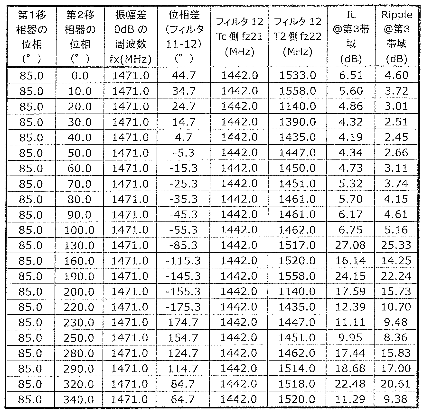
また、図9Aは、実施例3に係るフィルタ装置10Dのフィルタモードにおいて、フィルタ12の共通端子Tc側のインピーダンスを固定して入出力端子T2側のインピーダンスを変化させた場合の通過特性、位相差特性およびインピーダンス特性を表すグラフである。
また、図9Bは、実施例3に係るフィルタ装置10Dのフィルタモードにおけるフィルタ12の入出力端子T2側の位相を変化させた場合の第3帯域の挿入損失およびリップルを表すグラフである。図9Bの(a)は、フィルタ12のインピーダンス最大周波数と第3帯域の挿入損失およびリップルとの関係を表すグラフであり、図9Bの(b)は、図9Bの(a)のグラフを拡大したものである。また、図9Bの(c)は、フィルタ11および12の位相差と第3帯域の挿入損失およびリップルとの関係を表すグラフであり、図9Bの(d)は、図9Bの(c)のグラフを拡大したものである。
表1、図9A、図9Bの(a)および(b)より、フィルタ12の共通端子Tc側のインピーダンス最大周波数fz21および入出力端子T2側のインピーダンス最大周波数fz22が、第2帯域低域端の周波数以下であることにより、第3帯域を通過帯域とする広帯域のフィルタにおける通過帯域内の20dBを超える大きなリップルを、20dB以下へと低減できることがわかる。
また、表1、図9A、図9Bの(c)および(d)より、フィルタ11とフィルタ12との位相差が、-50°以上かつ+50°以下であることにより、第3帯域を通過帯域とする広帯域のフィルタにおける通過帯域内の10dBを超える大きなリップルを、10dB以下へと低減できることがわかる。
さらに、表1、図9A、図9Bの(a)および(b)より、フィルタ12単体の共通端子Tc側のインピーダンス最大周波数fz21および入出力端子T2側のインピーダンス最大周波数fz22が、第1帯域高域端の周波数以下であることにより、第3帯域を通過帯域とする広帯域のフィルタにおける通過帯域内の5dBを超える大きなリップルを、5dB以下へと低減できることがわかる。
表2は、実施例3に係るフィルタ装置10Dのフィルタモードにおいて、フィルタ12の入出力端子T2側のインピーダンスを固定して共通端子Tc側のインピーダンスを変化させた場合の第3帯域における挿入損失、リップル、フィルタ11および12の振幅差が0dBの周波数、フィルタ11および12の位相差、フィルタ12の共通端子Tc側のインピーダンスが最大となる周波数fz21、およびフィルタ12の入出力端子T2側のインピーダンスが最大となる周波数fz21を示している。なお、表2に示された第1移相器の位相および第2移相器の位相とは、それぞれ、フィルタ12が共通端子Tc側に有する第1移相器の位相、および、フィルタ12が入出力端子T2側に有する第2移相器の位相を示しており、フィルタ12は、上記第1移相器、上記第2移相器、および上記第1移相器と上記第2移相器との間に接続されたフィルタ回路で構成される。フィルタ12が、その両端に移相器を有することで、フィルタ12単体のインピーダンスが最大となる周波数、および、フィルタ11単体とフィルタ12単体との位相差を変化させることが可能となる。
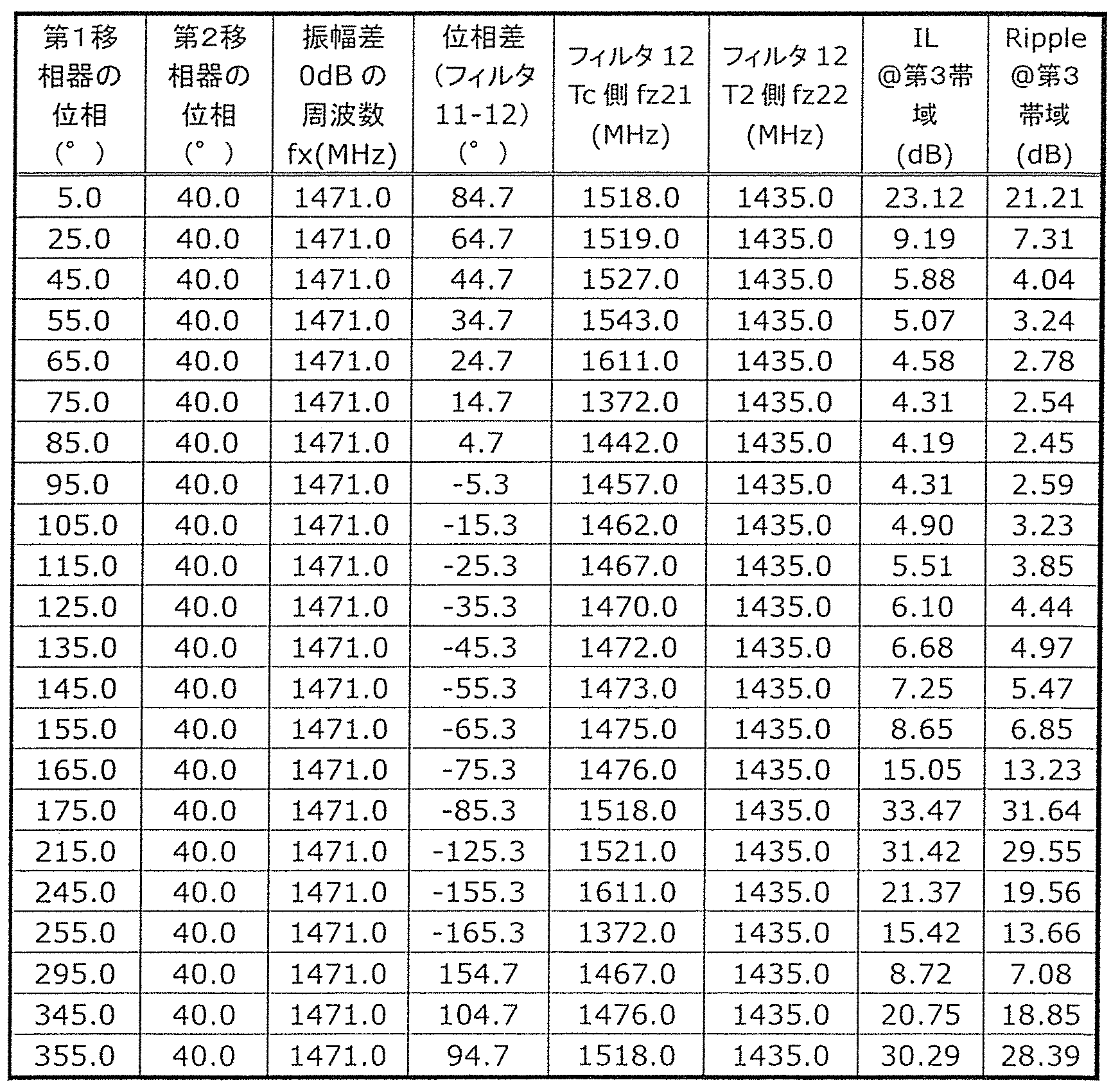
また、図10Aは、実施例3に係るフィルタ装置10Dのフィルタモードにおいて、フィルタ12の入出力端子T2側のインピーダンスを固定して共通端子Tc側のインピーダンスを変化させた場合の通過特性、位相差特性およびインピーダンス特性を表すグラフである。
また、図10Bは、実施例3に係るフィルタ装置10Dのフィルタモードにおけるフィルタ12の共通端子Tc側の位相を変化させた場合の第3帯域の挿入損失およびリップルを表すグラフである。図10Bの(a)は、フィルタ12のインピーダンス最大周波数と第3帯域の挿入損失およびリップルとの関係を表すグラフであり、図10Bの(b)は、図10Bの(a)のグラフを拡大したものである。また、図10Bの(c)は、フィルタ11および12の位相差と第3帯域の挿入損失およびリップルとの関係を表すグラフであり、図10Bの(d)は、図10Bの(c)のグラフを拡大したものである。
表2、図10A、図10Bの(a)および(b)より、フィルタ12の共通端子Tc側のインピーダンス最大周波数fz21および入出力端子T2側のインピーダンス最大周波数fz22が、第2帯域低域端の周波数以下であることにより、第3帯域を通過帯域とする広帯域のフィルタにおける通過帯域内の20dBを超える大きなリップルを、20dB以下へと低減できることがわかる。
また、表2、図10A、図10Bの(c)および(d)より、フィルタ11とフィルタ12との位相差が、-50°以上かつ+50°以下であることにより、第3帯域を通過帯域とする広帯域のフィルタにおける通過帯域内の10dBを超える大きなリップルを、10dB以下へと低減できることがわかる。
さらに、表2、図10A、図10Bの(a)および(b)より、フィルタ12単体の共通端子Tc側のインピーダンス最大周波数fz21および入出力端子T2側のインピーダンス最大周波数fz22が、第1帯域高域端の周波数以下であることにより、第3帯域を通過帯域とする広帯域のフィルタにおける通過帯域内の5dBを超える大きなリップルを、5dB以下へと低減できることがわかる。
表3は、実施例3に係るフィルタ装置10Dのフィルタモードにおいて、フィルタ12の共通端子Tc側および入出力端子T2側のインピーダンスを変化させた場合の第3帯域における挿入損失、リップル、フィルタ11および12の振幅差が0dBの周波数、フィルタ11および12の位相差、フィルタ12の共通端子Tc側のインピーダンスが最大となる周波数fz21、およびフィルタ12の入出力端子T2側のインピーダンスが最大となる周波数fz21を示している。なお、表3に示された第1移相器の位相および第2移相器の位相とは、それぞれ、フィルタ12が共通端子Tc側に有する第1移相器の位相、および、フィルタ12が入出力端子T2側に有する第2移相器の位相を示しており、フィルタ12は、上記第1移相器、上記第2移相器、および上記第1移相器と上記第2移相器との間に接続されたフィルタ回路で構成される。フィルタ12が、その両端に移相器を有することで、フィルタ12単体のインピーダンスが最大となる周波数、および、フィルタ11単体とフィルタ12単体との位相差を変化させることが可能となる。
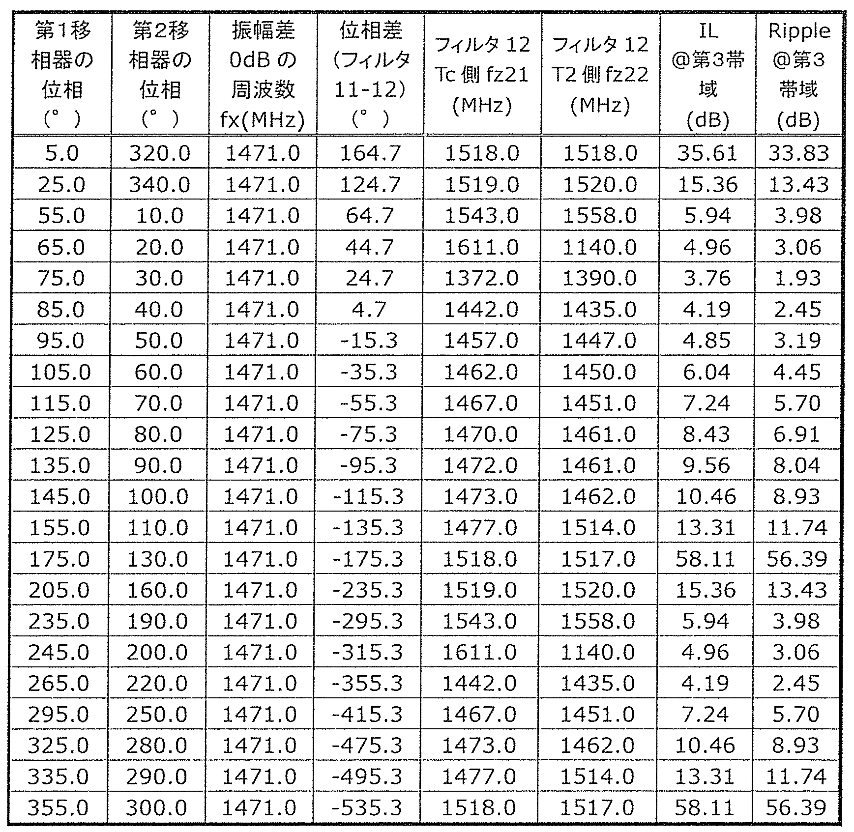
また、図11Aは、実施例3に係るフィルタ装置10Dのフィルタモードにおいて、フィルタ12の共通端子Tc側および入出力端子T2側のインピーダンスを変化させた場合の通過特性、位相差特性およびインピーダンス特性を表すグラフである。
また、図11Bは、実施例3に係るフィルタ装置10Dのフィルタモードにおけるフィルタ12の共通端子Tc側および入出力端子T2側の位相を変化させた場合の第3帯域の挿入損失およびリップルを表すグラフである。図11Bの(a)は、フィルタ12の共通端子Tc側のインピーダンス最大周波数fz21と第3帯域の挿入損失およびリップルとの関係を表すグラフであり、図11Bの(b)は、図11Bの(a)のグラフを拡大したものである。また、図11Bの(c)は、フィルタ12の入出力端子T2側のインピーダンス最大周波数fz22と第3帯域の挿入損失およびリップルとの関係を表すグラフであり、図11Bの(d)は、図11Bの(c)のグラフを拡大したものである。また、図11Bの(e)は、フィルタ11および12の位相差と第3帯域の挿入損失およびリップルとの関係を表すグラフであり、図11Bの(f)は、図11Bの(e)のグラフを拡大したものである。
表3、図11A、および図11Bの(a)~(d)より、フィルタ12の共通端子Tc側のインピーダンス最大周波数fz21および入出力端子T2側のインピーダンス最大周波数fz22が、第2帯域低域端の周波数以下であることにより、第3帯域を通過帯域とする広帯域のフィルタにおける通過帯域内の20dBを超える大きなリップルを、20dB以下へと低減できることがわかる。
また、表3、図11A、図11Bの(e)および(f)より、フィルタ11とフィルタ12との位相差が、-50°以上かつ+50°以下であることにより、第3帯域を通過帯域とする広帯域のフィルタにおける通過帯域内の10dBを超える大きなリップルを、10dB以下へと低減できることがわかる。
さらに、表3、図11A、図11Bの(a)~(d)より、フィルタ12の共通端子Tc側のインピーダンス最大周波数fz21および入出力端子T2側のインピーダンス最大周波数fz22が、第1帯域高域端の周波数以下であることにより、第3帯域を通過帯域とする広帯域のフィルタにおける通過帯域内の5dBを超える大きなリップルを、5dB以下へと低減できることがわかる。
なお、実施例3に係るフィルタ装置10Dの変形例として、変形例1に係るフィルタ装置10Bの構成と同様に、スイッチSW2およびSW3をフィルタ11と入出力端子T1との間に配置した構成が考えられる。この場合には、フィルタ11は、共通端子Tcと入出力端子T1(第2入出力端子)とを結ぶ第2経路上に接続され、第2帯域を通過帯域とする第2フィルタである。また、フィルタ12は、共通端子Tcと入出力端子T2(第1入出力端子)とを結ぶ第1経路上に接続され、第1帯域を通過帯域とする第1フィルタである。第2帯域は、第1帯域の周波数よりも低く、かつ、第1帯域の周波数と重ならない周波数帯域である。入出力端子T1は第2入出力端子に相当し、入出力端子T2は、第1入出力端子に相当する。フィルタ12(第1フィルタ)は、第1移相器、フィルタ回路、および第2移相器で構成される。
この場合には、フィルタ12の共通端子Tc側のインピーダンス最大周波数fz21および入出力端子T2側のインピーダンス最大周波数fz22が、第1帯域低域端の周波数以下であることにより、第3帯域を通過帯域とする広帯域のフィルタにおける通過帯域内の20dBを超える大きなリップルを、20dB以下へと低減できる。
また、フィルタ11とフィルタ12との位相差が、-50°以上かつ+50°以下であることにより、第3帯域を通過帯域とする広帯域のフィルタにおける通過帯域内の10dBを超える大きなリップルを、10dB以下へと低減できる。
さらに、フィルタ12の共通端子Tc側のインピーダンス最大周波数fz21および入出力端子T2側のインピーダンス最大周波数fz22が、第2帯域高域端の周波数以下であることにより、第3帯域を通過帯域とする広帯域のフィルタにおける通過帯域内の5dBを超える大きなリップルを、5dB以下へと低減できる。
[1.6 実施例3に係るフィルタ装置の移相器構成]
次に、実施例3に係るフィルタ装置10Dのフィルタ12を構成する移相器の構成について説明する。
次に、実施例3に係るフィルタ装置10Dのフィルタ12を構成する移相器の構成について説明する。
図12は、実施例3に係るフィルタ装置10Dの具体的回路構成図である。
フィルタ11は、共通端子TcとノードX1とを結ぶ経路上に配置された直列腕共振子s11、s12およびs13と、共通端子TcとノードX1とを結ぶ経路上の各ノードとグランドとの間に配置された並列腕共振子p11、p12、p13およびp14とを備える。上記構成により、フィルタ11は、第1帯域を通過帯域とするラダー型のバンドパスフィルタを構成している。
フィルタ12は、共通端子TcとノードX2とを結ぶ第2経路上に配置された直列腕共振子s21、s22およびs23と、第2経路上の各ノードとグランドとの間に配置された並列腕共振子p21、p22、p23およびp24と、移相器21および22と、入出力端子T3およびT4と、を備える。直列腕共振子s21~s23、および、並列腕共振子p21~p24は、共振特性を有するフィルタ部12Rを構成している。移相器21は、フィルタ部12Rの一方の端子と入出力端子T3(第3入出力端子)との間に接続された第1移相器であり、移相器22は、フィルタ部12Rの他方の端子と入出力端子T4(第4入出力端子)との間に接続された第2移相器である。移相器21および22は、分布定数線路で構成される遅延線、または、集中定数素子で構成される。上記構成によれば、フィルタ12は、第2帯域を通過帯域とする位相調整が可能なラダー型のバンドパスフィルタを構成している。
表4に、実施例3に係るフィルタ装置10Dの回路パラメータの一例を示す。
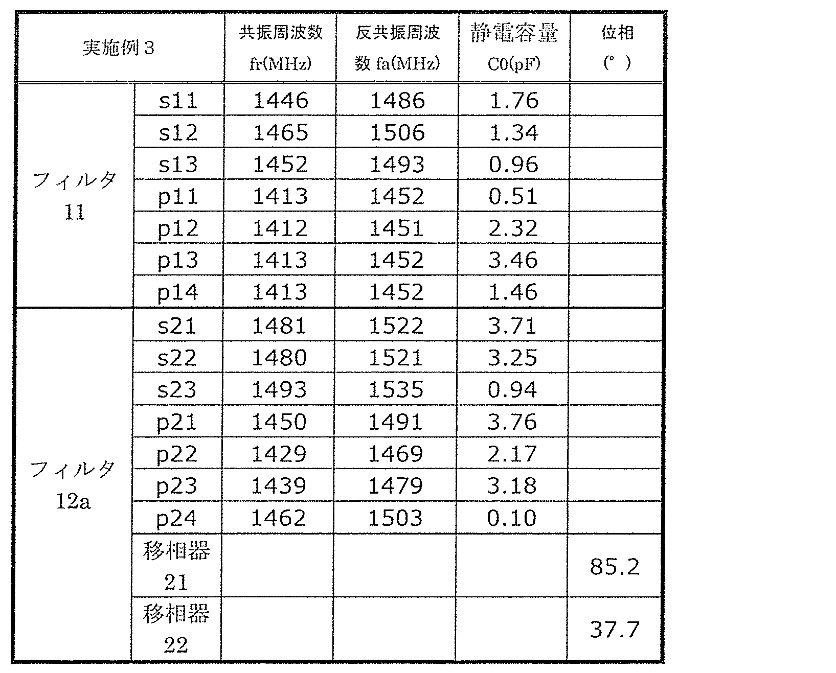
図13Aは、変形例2に係るフィルタ装置10D1の回路構成図である。同図に示されたフィルタ装置10D1は、フィルタ装置10Dの移相器21および22の具体的回路構成を示したものである。本変形例に係るフィルタ装置10D1は、フィルタ11および12aと、スイッチSW1~SW4と、共通端子Tcと、入出力端子T1およびT2と、を備える。
フィルタ12aは、フィルタ部12Rと、移相器21aおよび22aと、入出力端子T3およびT4と、を有している。
移相器21aおよび22aは、キャパシタまたはインダクタで構成されるインピーダンス素子を有している。具体的には、移相器21aは、第2経路上に配置されたキャパシタCs11およびCs12と、キャパシタCs11およびCs12の接続ノードとグランドとの間に接続されたインダクタLp1と、を有している。また、移相器22aは、第2経路上に配置されたキャパシタCs21およびCs22と、キャパシタCs21およびCs22の接続ノードとグランドとの間に接続されたインダクタLp2と、を有している。つまり、本変形例に係る移相器21aおよび22aは、それぞれ、(T型3次の)高域通過フィルタ型の回路構成を有している。
表4に示されたように、実施例3に係るフィルタ装置10Dでは、移相器21および22の位相は、ともに正値(+側の位相)であるため、高域通過フィルタ型の回路構成が適している。
図13Bは、変形例2に係るフィルタ装置10D1の通過特性を表すグラフである。同図の(a)には、スイッチSW1およびSW3をオン、スイッチSW2およびSW4をオフとした場合の共通端子Tc-入出力端子T1間の通過特性が示されている。また、同図の(b)には、スイッチSW1およびSW3をオフ、スイッチSW2およびSW4をオンとした場合の共通端子Tc-入出力端子T1間の通過特性が示されている。また、同図の(c)には、スイッチSW1およびSW3をオフ、スイッチSW2およびSW4をオンとした場合の共通端子Tc-入出力端子T2間の通過特性が示されている。
なお、本変形例を含む以降の変形例2~5では、フィルタ11の第1帯域を、LTEのBand11の送信帯域およびBand21の送信帯域を含む帯域としている。また、フィルタ12aの第2帯域を、LTEのBand11の受信帯域およびBand21の受信帯域を含む帯域としている。また、第1帯域の少なくとも一部と第2帯域の少なくとも一部とを含む第3帯域を、LTEのBand32の受信帯域を含む帯域としている。
図13Bの(a)に示すように、スイッチSW1およびSW3をオンとし、スイッチSW2およびSW4をオフとした場合、フィルタ装置10D1は、共通端子Tcと入出力端子T1との間で、第1帯域および第2帯域を含む相対的に広帯域の第3帯域を有するフィルタを構成する。ここで、移相器21aおよび22aの位相を表4に示す値に調整することにより、フィルタ11とフィルタ12aとの位相差を最適化することが可能となる。また、キャパシタおよびインダクタなどの集中定数素子を用いることにより、フィルタ11とフィルタ12aとの位相差を最適化することが可能になるとともに、移相器21aおよび移相器22aを小型にできる。よって、第1帯域および第2帯域を含む相対的に広帯域の第3帯域を有するフィルタのリップルを改善することが可能となる。図13Bの(a)では、第3帯域の(最大)挿入損失が4.15dBとなっており、第3帯域の低損失および低リップルが実現されていることがわかる。
図14Aは、変形例3に係るフィルタ装置10D2の回路構成図である。同図に示されたフィルタ装置10D2は、フィルタ装置10Dの移相器21および22の具体的回路構成を示したものである。本変形例に係るフィルタ装置10D2は、フィルタ11および12bと、スイッチSW1~SW4と、共通端子Tcと、入出力端子T1およびT2と、を備える。
フィルタ12bは、フィルタ部12Rと、移相器21bおよび22bと、入出力端子T3およびT4と、を有している。
移相器21bおよび22bは、キャパシタまたはインダクタで構成されるインピーダンス素子を有している。具体的には、移相器21bは、第2経路上に配置されたキャパシタCs1と、キャパシタCs1および入出力端子T3の接続ノードとグランドとの間に接続されたインダクタLp1と、を有している。また、移相器22aは、第2経路上に配置されたキャパシタCs2と、キャパシタCs2および入出力端子T4の接続ノードとグランドとの間に接続されたインダクタLp2と、を有している。つまり、本変形例に係る移相器21bおよび22bは、それぞれ、(T型2次の)高域通過フィルタ型の回路構成を有している。
表4に示されたように、実施例3に係るフィルタ装置10Dでは、移相器21および22の位相は、ともに正値(+側の位相)であるため、高域通過フィルタ型の回路構成が適している。
図14Bは、変形例3に係るフィルタ装置10D2の通過特性を表すグラフである。同図の(a)には、スイッチSW1およびSW3をオン、スイッチSW2およびSW4をオフとした場合の共通端子Tc-入出力端子T1間の通過特性が示されている。また、同図の(b)には、スイッチSW1およびSW3をオフ、スイッチSW2およびSW4をオンとした場合の共通端子Tc-入出力端子T1間の通過特性が示されている。また、同図の(c)には、スイッチSW1およびSW3をオフ、スイッチSW2およびSW4をオンとした場合の共通端子Tc-入出力端子T2間の通過特性が示されている。
図14Bの(a)に示すように、スイッチSW1およびSW3をオンとし、スイッチSW2およびSW4をオフとした場合、フィルタ装置10D2は、共通端子Tcと入出力端子T1との間で、第1帯域および第2帯域を含む相対的に広帯域の第3帯域を有するフィルタを構成する。ここで、移相器21bおよび22bの位相を表4に示す値に調整することにより、フィルタ11とフィルタ12との位相差を最適化することが可能となる。また、キャパシタおよびインダクタなどの集中定数素子を用いることにより、フィルタ11とフィルタ12bとの位相差を最適化することが可能になるとともに、移相器21bおよび移相器22bを小型にできる。よって、第1帯域および第2帯域を含む相対的に広帯域の第3帯域を有するフィルタのリップルを改善することが可能となる。図14Bの(a)では、第3帯域の(最大)挿入損失が5.32dBとなっており、第3帯域の低損失および低リップルが実現されていることがわかる。
図15Aは、変形例4に係るフィルタ装置10D3の回路構成図である。同図に示されたフィルタ装置10D3は、フィルタ装置10Dの移相器21および22の具体的回路構成を示したものである。本変形例に係るフィルタ装置10D3は、フィルタ11および12cと、スイッチSW1~SW4と、共通端子Tcと、入出力端子T1およびT2と、を備える。
フィルタ12cは、フィルタ部12Rと、移相器21cおよび22cと、入出力端子T3およびT4と、を有している。
移相器21cおよび22cは、キャパシタまたはインダクタで構成されるインピーダンス素子を有している。具体的には、移相器21cは、第2経路上に配置されたキャパシタCs1と、キャパシタCs1およびフィルタ部12Rの接続ノードとグランドとの間に接続されたインダクタLp1と、を有している。また、移相器22cは、第2経路上に配置されたキャパシタCs2と、キャパシタCs2およびフィルタ部12Rの接続ノードとグランドとの間に接続されたインダクタLp2と、を有している。つまり、本変形例に係る移相器21cおよび22cは、それぞれ、(T型2次の)高域通過フィルタ型の回路構成を有している。
表4に示されたように、実施例3に係るフィルタ装置10Dでは、移相器21および22の位相は、ともに正値(+側の位相)であるため、高域通過フィルタ型の回路構成が適している。
図15Bは、変形例4に係るフィルタ装置10D3の通過特性を表すグラフである。同図の(a)には、スイッチSW1およびSW3をオン、スイッチSW2およびSW4をオフとした場合の共通端子Tc-入出力端子T1間の通過特性が示されている。また、同図の(b)には、スイッチSW1およびSW3をオフ、スイッチSW2およびSW4をオンとした場合の共通端子Tc-入出力端子T1間の通過特性が示されている。また、同図の(c)には、スイッチSW1およびSW3をオフ、スイッチSW2およびSW4をオンとした場合の共通端子Tc-入出力端子T2間の通過特性が示されている。
図15Bの(a)に示すように、スイッチSW1およびSW3をオンとし、スイッチSW2およびSW4をオフとした場合、フィルタ装置10D3は、共通端子Tcと入出力端子T1との間で、第1帯域および第2帯域を含む相対的に広帯域の第3帯域を有するフィルタを構成する。ここで、移相器21cおよび22cの位相を表4に示す値に調整することにより、フィルタ11とフィルタ12との位相差を最適化することが可能となる。また、キャパシタおよびインダクタなどの集中定数素子を用いることにより、フィルタ11とフィルタ12cとの位相差を最適化することが可能になるとともに、移相器21cおよび移相器22cを小型にできる。よって、第1帯域および第2帯域を含む相対的に広帯域の第3帯域を有するフィルタのリップルを改善することが可能となる。図15Bの(a)では、第3帯域の(最大)挿入損失が5.05dBとなっており、第3帯域の低損失および低リップルが実現されていることがわかる。
図16Aは、変形例5に係るフィルタ装置10D4の回路構成図である。同図に示されたフィルタ装置10D4は、フィルタ装置10Dの移相器21および22の具体的回路構成を示したものである。本変形例に係るフィルタ装置10D4は、フィルタ11および12dと、スイッチSW1~SW4と、共通端子Tcと、入出力端子T1およびT2と、を備える。
フィルタ12dは、フィルタ部12Rと、移相器21dおよび22dと、入出力端子T3およびT4と、を有している。
移相器21dおよび22dは、キャパシタまたはインダクタで構成されるインピーダンス素子を有している。具体的には、移相器21dは、第2経路上に配置されたインダクタLs11およびLs12と、インダクタLs11およびLs12の接続ノードとグランドとの間に接続されたキャパシタCp1と、を有している。また、移相器22dは、第2経路上に配置されたインダクタLs21およびLs22と、インダクタLs21およびLs22の接続ノードとグランドとの間に接続されたキャパシタCp2と、を有している。つまり、本変形例に係る移相器21dおよび22dは、それぞれ、(T型3次の)低域通過フィルタ型の回路構成を有している。
表4に示されたように、実施例3に係るフィルタ装置10Dでは、移相器21および22の位相は、ともに正値(+側の位相)であるが、本変形例のような低域通過フィルタ型の回路構成であっても位相調整が可能となる。なお、低域通過フィルタ型の回路構成を有する移相器は、負値(-側の位相)に調整される場合に適している。
図16Bは、変形例5に係るフィルタ装置10D4の通過特性を表すグラフである。同図の(a)には、スイッチSW1およびSW3をオン、スイッチSW2およびSW4をオフとした場合の共通端子Tc-入出力端子T1間の通過特性が示されている。また、同図の(b)には、スイッチSW1およびSW3をオフ、スイッチSW2およびSW4をオンとした場合の共通端子Tc-入出力端子T1間の通過特性が示されている。また、同図の(c)には、スイッチSW1およびSW3をオフ、スイッチSW2およびSW4をオンとした場合の共通端子Tc-入出力端子T2間の通過特性が示されている。
図16Bの(a)に示すように、スイッチSW1およびSW3をオンとし、スイッチSW2およびSW4をオフとした場合、フィルタ装置10D4は、共通端子Tcと入出力端子T1との間で、第1帯域および第2帯域を含む相対的に広帯域の第3帯域を有するフィルタを構成する。ここで、移相器21dおよび22dの位相を表4に示す値に調整することにより、フィルタ11とフィルタ12との位相差を最適化することが可能となる。また、キャパシタおよびインダクタなどの集中定数素子を用いることにより、フィルタ11とフィルタ12dとの位相差を最適化することが可能になるとともに、移相器21dおよび移相器22dを小型にできる。よって、第1帯域および第2帯域を含む相対的に広帯域の第3帯域を有するフィルタのリップルを改善することが可能となる。図15Bの(a)では、第3帯域の(最大)挿入損失が5.06dBとなっており、第3帯域の低損失および低リップルが実現されていることがわかる。
なお、変形例2~変形例5において、第1移相器と第2移相器とを同じ回路構成としたが、これに限られない。本発明に係るフィルタ装置として必要な第1フィルタと第2フィルタとの位相差を実現するため、第1移相器と第2移相器とが異なる回路構成であってもよい。例えば、第1移相器が低域通過フィルタ型の回路構成を有し、第2移相器が高域通過フィルタ型の回路構成を有していてもよく、また、その逆であってもよい。
図17Aは、変形例5に係るフィルタ装置10D4の広帯域通過特性を表すグラフである。また、図17Bは、変形例2に係るフィルタ装置10D1の広帯域通過特性を表すグラフである。図17Aおよび図17Bの双方において、(a)には、スイッチSW1およびSW3をオン、スイッチSW2およびSW4をオフとした場合の共通端子Tc-入出力端子T1間の通過特性が示されている。また、(b)には、スイッチSW1およびSW3をオフ、スイッチSW2およびSW4をオンとした場合の共通端子Tc-入出力端子T1間の通過特性が示されている。また、(c)には、スイッチSW1およびSW3をオフ、スイッチSW2およびSW4をオンとした場合の共通端子Tc-入出力端子T2間の通過特性が示されている。
図17Aに示すように、低域通過フィルタ型の回路構成を有する移相器21dおよび22dを用いたフィルタ装置10D4では、通過帯域高域側の減衰特性が向上する。一方、図17Bに示すように、高域通過フィルタ型の回路構成を有する移相器21aおよび22aを用いたフィルタ装置10D1では、通過帯域高域側の減衰特性が向上する。よって、例えば、高調波およびバルク波などのスプリアスの発生周波数に応じて、低域通過フィルタ型の移相器および高域通過フィルタ型の移相器を選択してもよい。
[1.7 実施例4に係るフィルタ装置]
図18は、実施例4に係るフィルタ装置10Eの回路構成図である。同図に示されたフィルタ装置10Eは、フィルタ11、12eおよび13と、スイッチSW1、SW2、SW3およびSW4と、共通端子Tcと、入出力端子T1およびT2と、を備える。本実施例に係るフィルタ装置10Eは、実施例3に係るフィルタ装置10Dと比較して、第2フィルタの回路構成、および、フィルタ13が付加されている点が構成として異なる。以下、本実施例に係るフィルタ装置10Eについて、実施例3に係るフィルタ装置10Dと同じ点は説明を省略し、異なる点を中心に説明する。
図18は、実施例4に係るフィルタ装置10Eの回路構成図である。同図に示されたフィルタ装置10Eは、フィルタ11、12eおよび13と、スイッチSW1、SW2、SW3およびSW4と、共通端子Tcと、入出力端子T1およびT2と、を備える。本実施例に係るフィルタ装置10Eは、実施例3に係るフィルタ装置10Dと比較して、第2フィルタの回路構成、および、フィルタ13が付加されている点が構成として異なる。以下、本実施例に係るフィルタ装置10Eについて、実施例3に係るフィルタ装置10Dと同じ点は説明を省略し、異なる点を中心に説明する。
フィルタ11は、実施例3に係るフィルタ11と同じ回路構成であり、直列腕共振子s11~s13と、並列腕共振子p11~p14とを備える。上記構成により、フィルタ11は、第1帯域を通過帯域とするラダー型のバンドパスフィルタを構成している。
フィルタ12eは、共通端子TcとノードX2とを結ぶ第2経路上であって共通端子TcとノードX2との間に配置された直列腕共振子s21と、第2経路上であって共通端子TcとノードX2との間の各ノードとグランドとの間に配置された並列腕共振子p21およびp22と、移相器21および22と、を備える。直列腕共振子s21、並列腕共振子p21およびp22は、共振特性を有するフィルタ回路を構成している。移相器21は、フィルタ回路の一方の端子と共通端子Tcとの間に接続された第1移相器であり、移相器22は、フィルタ回路の他方の端子とノードX2との間に接続された第2移相器である。
フィルタ13は、第2経路上であってスイッチSW2と入出力端子T2との間に接続され、第2帯域を通過帯域とする第3フィルタである。フィルタ13は、ノードX3と入出力端子T2とを結ぶ経路に配置された直列腕共振子s31および縦結合型共振器32と、縦結合型共振器32と入出力端子T2とを結ぶノードとグランドとの間に接続された並列腕共振子p31と、を備える。縦結合型共振器32は、例えば、5つのIDT電極と当該5つのIDT電極の並び方向の両端に配置された反射器とで構成されている。なお、縦結合型共振器32のIDT電極の数は2つ以上であればよく、反射器はなくてもよい。
表5に、実施例4に係るフィルタ装置10Eの回路パラメータの一例を示す。なお、縦結合型共振器32の回路パラメータについては省略した。
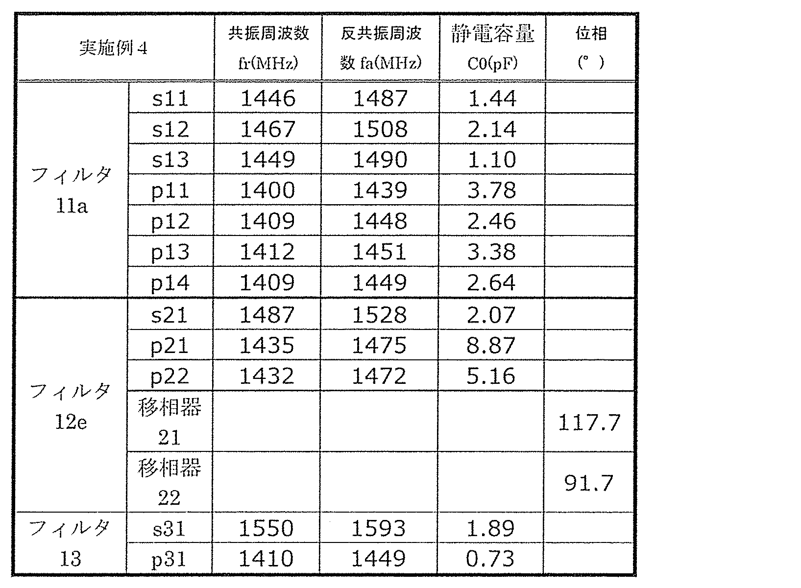
図19は、実施例4に係るフィルタ装置10Eの通過特性、振幅特性、位相特性およびインピーダンス特性を表すグラフである。同図の(a)には、フィルタ装置10Eのフィルタモードにおける通過特性が示されている。同図の(b)および(c)には、フィルタ装置10Eのマルチプレクサモードにおける通過特性が示されている。同図の(d)には、フィルタ11単体、フィルタ12e単体およびフィルタ13単体の振幅特性、フィルタ11単体およびフィルタ12e単体の振幅差が示されている。同図の(e)には、フィルタ11単体およびフィルタ12e単体の位相特性、ならびにそれらの位相差が示されている。同図の(f)には、共通端子Tcからフィルタ11単体およびフィルタ12e単体を見たインピーダンス特性が示されている。同図の(g)には、入出力端子T1からフィルタ11単体を見たインピーダンス特性および入出力端子T2からフィルタ12e単体を見たインピーダンス特性が示されている。
また、図20は、実施例3に係るフィルタ装置10Dおよび実施例4に係るフィルタ装置10Eの通過特性を比較したグラフである。同図の(a)には、スイッチSW1およびSW3をオン、スイッチSW2およびSW4をオフとした場合の共通端子Tc-入出力端子T1間の通過特性の比較が示されている。また、同図の(b)には、スイッチSW1およびSW3をオフ、スイッチSW2およびSW4をオンとした場合の共通端子Tc-入出力端子T1間の通過特性の比較が示されている。また、同図の(c)には、スイッチSW1およびSW3をオフ、スイッチSW2およびSW4をオンとした場合の共通端子Tc-入出力端子T2間の通過特性の比較が示されている。
実施例4に係るフィルタ装置10Eの上記構成によれば、図19の(a)および図20の(a)に示すように、スイッチSW1がオンかつスイッチSW2がオフの場合であって共通端子Tcと入出力端子T1との間で第3帯域を通過帯域とするフィルタが機能している場合、フィルタ13は機能せず、第3帯域のリップルが低減された通過特性となっている。一方、スイッチSW1素子がオフかつスイッチSW2がオンの場合であってマルチプレクサが機能している場合、図19の(c)および図20の(c)に示すように、共通端子Tcと入出力端子T2との間でフィルタ13が機能し、共通端子Tcと入出力端子T2との間で構成される第2帯域を通過帯域とするフィルタの通過帯域外の減衰特性が向上する。
また、図19の(d)に示すように、フィルタ13単体の通過特性における第2帯域低域側の急峻度は、フィルタ12単体の通過特性における第2帯域低域側の急峻度よりも高い。
共通端子Tcと入出力端子T1との間で、第3帯域を通過帯域とする広帯域のフィルタが機能している場合、フィルタ12eの第2帯域低域側の急峻度が高いほど、第3帯域にリップルが生じ易くなる。一方、当該フィルタ装置がマルチプレクサとして機能している場合、フィルタ12eの第2帯域低域側の急峻度が高いほど、入出力端子T1と入出力端子T2との間において、第1帯域のアイソレーション(減衰量)は向上する。
これに対して、本実施例に係るフィルタ装置10Eによれば、第2帯域低域側の急峻度が高く、第3帯域の構成には寄与しないフィルタ13が配置されるので、第3帯域を通過帯域とするフィルタは、フィルタ11およびフィルタ12eで構成されるので、第3帯域を通過帯域とするフィルタのリップルを低減しつつ、フィルタ11と、フィルタ12eおよび13が縦続接続されたフィルタ回路とで構成されたマルチプレクサの減衰特性およびアイソレーション特性を向上させることが可能となる。
さらに、フィルタ13の配置により、マルチプレクサを構成するフィルタ12eの共振子構成を少なくできる。つまり、フィルタ12eを構成する共振子次数を小さくでき第2帯域を広帯域化できるので、第3帯域のリップルを低減できる。
また、図19の(f)および(g)に示すように、実施例4に係るフィルタ装置10Eにおいて、フィルタ12eのインピーダンスが最大となる周波数を調整することで、第3帯域を通過帯域とする広帯域フィルタのリップルを改善することが可能となる。
なお、本実施例では、第2経路側にフィルタ13が接続されているが、ノードX2と入出力端子T2との間にスイッチSW2およびSW3ならびにフィルタ13が配置されているが、ノードX1と入出力端子T1との間にスイッチSW2およびSW3ならびにフィルタ13が配置されていてもよい。この場合、マルチプレクサとして機能する場合、第2帯域を通過帯域とするフィルタ特性において、第1帯域である減衰特性が向上する。
より具体的には、実施例4に係るフィルタ装置10Eの変形例として、スイッチSW2およびSW3ならびにフィルタ13をノードX1と入出力端子T1との間に接続した構成が考えられる。この場合には、フィルタ11は、共通端子Tcと入出力端子T1(第2入出力端子)とを結ぶ第2経路上に接続され、第2帯域を通過帯域とする第2フィルタである。また、フィルタ12eは、共通端子Tcと入出力端子T2(第1入出力端子)とを結ぶ第1経路上に接続され、第1帯域を通過帯域とする第1フィルタである。第2帯域は、第1帯域の周波数よりも低く、かつ、第1帯域の周波数と重ならない周波数帯域である。入出力端子T1は第2入出力端子に相当し、入出力端子T2は、第1入出力端子に相当する。フィルタ12e(第1フィルタ)は、第1移相器、フィルタ回路、および第2移相器で構成される。
また、フィルタ13単体の通過特性における第2帯域高域側の急峻度は、フィルタ11単体の通過特性における第2帯域高域側の急峻度よりも高い。
共通端子Tcと入出力端子T2との間で、第3帯域を通過帯域とする広帯域のフィルタが機能している場合、フィルタ11の第2帯域高域側の急峻度が高いほど、第3帯域にリップルが生じ易くなる。一方、当該フィルタ装置がマルチプレクサとして機能している場合、フィルタ11の第2帯域高域側の急峻度が高いほど、入出力端子T1と入出力端子T2との間において、第1帯域のアイソレーションは向上する。
これに対して、本構成によれば、第2帯域高域側の急峻度が高く、第3帯域の構成には寄与しないフィルタ13が配置されるので、第3帯域を通過帯域とするフィルタは、フィルタ11およびフィルタ12eで構成されるので、第3帯域を通過帯域とするフィルタのリップルを低減しつつ、フィルタ11および13が縦続接続されたフィルタ回路と、フィルタ12eとで構成されたマルチプレクサの減衰特性およびアイソレーション特性を向上させることが可能となる。
さらに、フィルタ13の配置により、マルチプレクサを構成するフィルタ11の共振子構成を少なくできる。つまり、フィルタ11を構成する共振子次数を小さくでき第2帯域を広帯域化できるので、第3帯域のリップルを低減できる。
[1.8 実施例5に係るフィルタ装置]
本実施例では、第1フィルタまたは第2フィルタが、スイッチ素子を有するインピーダンス回路が付加された直列腕回路または並列腕回路を有する構成について説明する。
本実施例では、第1フィルタまたは第2フィルタが、スイッチ素子を有するインピーダンス回路が付加された直列腕回路または並列腕回路を有する構成について説明する。
図21Aは、実施例5に係るフィルタ装置10Fの回路構成図である。同図に示されたフィルタ装置10Fは、フィルタ11a、12eおよび13と、スイッチSW1、SW2、SW3およびSW4と、共通端子Tcと、入出力端子T1およびT2と、を備える。本実施例に係るフィルタ装置10Fは、実施例4に係るフィルタ装置10Eと比較して、フィルタ11aの回路構成が異なる。以下、本実施例に係るフィルタ装置10Fについて、実施例4に係るフィルタ装置10Eと同じ点は説明を省略し、異なる点を中心に説明する。
フィルタ11aは、共通端子TcとノードX1とを結ぶ経路上に配置された直列腕共振子s11、s12およびs13と、共通端子TcとノードX1とを結ぶ経路上の各ノードとグランドとの間に配置された並列腕共振子p11、p12、p13およびp14と、スイッチSW11、SW12およびSW13と、キャパシタC11、C12およびC13と、を備える。なお、直列腕共振子s11、s12およびs13のそれぞれは、共通端子TcとノードX1とを結ぶ経路上に配置された直列腕回路であってもよい。並列腕共振子p11、p12、p13およびp14のそれぞれは、共通端子TcとノードX1とを結ぶ経路上の各ノードとグランドとの間に配置された並列腕回路であってもよい。直列腕回路および並列腕回路は、弾性波共振子で構成されていなくてもよく、インダクタやキャパシタなどの回路素子で構成されていてもよい。
直列腕共振子s11および共通端子Tcの接続ノードにはキャパシタC11の一端が接続され、キャパシタC11の他端と直列腕共振子s11およびs12の接続ノードとの間にはスイッチSW11が接続されている。
直列腕共振子s11およびs12の接続ノードにはキャパシタC12の一端が接続され、キャパシタC12の他端と直列腕共振子s12およびs13の接続ノードとの間にはスイッチSW12が接続されている。
直列腕共振子s12およびs13の接続ノードにはキャパシタC13の一端が接続され、キャパシタC13の他端と直列腕共振子s13およびノードX1の接続ノードとの間にはスイッチSW13が接続されている。
上記構成により、フィルタ11aは、スイッチSW11~SW13がオンの場合、第1a帯域(Band11Tx)を通過帯域とし、スイッチSW11~SW13がオフの場合、第1帯域(Band21Tx)を通過帯域する周波数可変型のバンドパスフィルタを構成している。
ここで、第1の直列腕回路は、直列腕共振子s11と、直列腕共振子s11に並列接続された第1のインピーダンス回路とを有している。第1のインピーダンス回路は、キャパシタC11とスイッチSW11とが直列接続された回路である。第2の直列腕回路は、直列腕共振子s12と、直列腕共振子s12に並列接続された第2のインピーダンス回路とを有している。第2のインピーダンス回路は、キャパシタC12とスイッチSW12とが直列接続された回路である。第3の直列腕回路は、直列腕共振子s13と、直列腕共振子s13に並列接続された第3のインピーダンス回路とを有している。第3のインピーダンス回路は、キャパシタC13とスイッチSW13とが直列接続された回路である。
表6に、実施例5に係るフィルタ装置10Fの回路パラメータを示す。
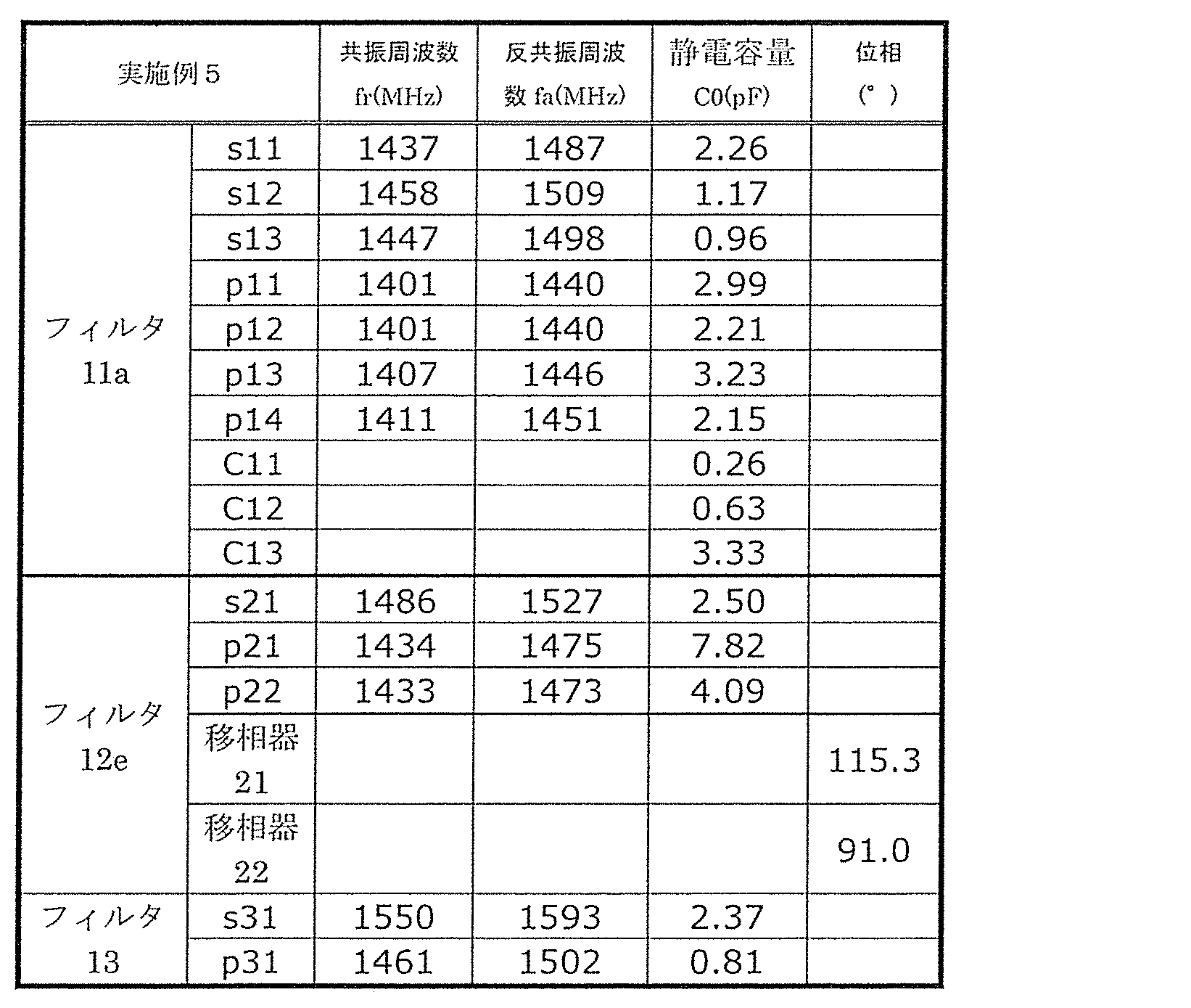
図22Aは、実施例5に係るフィルタ装置10Fの通過特性、振幅特性、位相特性およびインピーダンス特性を表すグラフである。また、図22Bは、実施例5に係るフィルタ装置10Fの第1a帯域および第2a帯域のデュプレクサモードにおける通過特性を表すグラフである。図22Aの(a)には、フィルタ装置10Fのフィルタモードにおける通過特性が示されている。図22Aの(b)および(c)には、それぞれ、フィルタ装置10Fのマルチプレクサモードにおける第1帯域(Band21Tx)および第2帯域(Band21Rx)の通過特性が示されている。図22Aの(d)には、フィルタ11a単体、フィルタ12e単体およびフィルタ13単体の振幅特性、フィルタ11a単体およびフィルタ12e単体の振幅差が示されている。図22Aの(e)には、フィルタ11a単体およびフィルタ12e単体の位相特性、ならびにそれらの位相差が示されている。図22Aの(f)には、共通端子Tcからフィルタ11a単体およびフィルタ12e単体を見たインピーダンス特性が示されている。図22Aの(g)には、入出力端子T1からフィルタ11a単体を見たインピーダンス特性および入出力端子T2からフィルタ12e単体を見たインピーダンス特性が示されている。図22Bの(a)および(b)には、フィルタ装置10Fのマルチプレクサモードにおける第1a帯域(Band11Tx)および第2a帯域(Band11Rx)の通過特性が示されている。
フィルタ11aにおいて、キャパシタC11~C13のそれぞれは、スイッチSW11~SW13がオンの場合、直列腕共振子s11~s13のそれぞれに、一対一で並列接続されるので、スイッチSW11~SW13がオフからオンへと切り替わることにより、各直列腕回路の反共振周波数が低域側へと切り替えられる。
なお、本実施の形態において、直列腕共振子、並列腕共振子、直列腕回路および並列腕回路のインピーダンス|Z|が極小となる周波数が共振周波数であり、インピーダンス|Z|が極大となる周波数が反共振周波数である。
直列腕回路の反共振周波数は、ラダー型フィルタにおける通過帯域高域側の減衰極を規定することから、図22Aの(b)および図22Bの(a)に示すように、フィルタ11aは、スイッチSW11~SW13のオンおよびオフの切り替えにより、通過帯域高域側の急峻度および通過帯域高域端の周波数が可変する。
また、スイッチSW11~SW13がオフからオンへと切り替わることで、フィルタ11aの通過帯域の高域側減衰極の周波数が低域側へ可変する(フィルタ11aの通過帯域がBand21TxからBand11Txへ切り替わる)ことで、(Band11Rxを通過帯域とする)フィルタ12eの低域側減衰量が向上する。
また、図22Aの(f)および(g)より、フィルタ12eの共通端子Tc側のインピーダンス最大周波数fz21および入出力端子T2側のインピーダンス最大周波数fz22が、第2帯域低域端の周波数以下である。これにより、第3帯域を通過帯域とする広帯域のフィルタにおける通過帯域内の20dBを超える大きなリップルを、20dB以下へと低減できる。
また、図22Aの(d)および(e)より、フィルタ11a単体の振幅とフィルタ12e単体の振幅とが等しくなる周波数において、フィルタ11aとフィルタ12eとの位相差が、-50°以上かつ+50°以下である。これにより、第3帯域を通過帯域とする広帯域のフィルタにおける通過帯域内の10dBを超える大きなリップルを、10dB以下へと低減できる。
さらに、図22Aの(f)および(g)より、フィルタ12eの共通端子Tc側のインピーダンス最大周波数fz21および入出力端子T2側のインピーダンス最大周波数fz22が、第1帯域高域端の周波数以下である。これにより、第3帯域を通過帯域とする広帯域のフィルタにおける通過帯域内の5dBを超える大きなリップルを、5dB以下へと低減できる。
本実施例に係るフィルタ装置10Fの構成によれば、(1)第1帯域(または第1a帯域)および第2帯域(または第2a帯域)を含む相対的に広帯域の通過帯域を有するフィルタ、および、第1帯域(または第1a帯域)である相対的に狭帯域の通過帯域および第2帯域(または第2a帯域)である相対的に狭帯域の通過帯域を合波または分波するマルチプレクサの双方について、通過帯域を可変させつつ、広帯域の通過帯域(第3帯域)のリップルを低減することが可能となる。
なお、実施例5に係るフィルタ装置10Fのフィルタ11aは、図21Bに示されたフィルタ11bであってもよい。フィルタ11bは、共通端子TcとノードX1とを結ぶ経路上に配置された直列腕共振子s11、s12およびs13と、共通端子TcとノードX1とを結ぶ経路上の各ノードとグランドとの間に配置された並列腕共振子p11、p12、p13およびp14と、スイッチSW11、SW12およびSW13と、キャパシタC11、C12およびC13と、を備える。フィルタ11bは、フィルタ11aと比較して、スイッチSW11、SW12およびSW13、ならびに、キャパシタC11、C12およびC13の接続形態のみが異なる。以下、フィルタ11bについて、フィルタ11aと異なる点のみを説明する。
直列腕共振子s11および共通端子Tcの接続ノードにはキャパシタC11の一端が接続され、キャパシタC11の他端と直列腕共振子s11およびs12の接続ノードとの間にはスイッチSW11が接続されている。
キャパシタC11の他端には、キャパシタC12の一端が接続され、キャパシタC12の他端と直列腕共振子s12およびs13の接続ノードとの間にはスイッチSW12が接続されている。
キャパシタC12の他端には、キャパシタC13の一端が接続され、キャパシタC13の他端と直列腕共振子s13およびノードX1の接続ノードとの間にはスイッチSW13が接続されている。
実施例5に係るフィルタ装置10Fにおいて、上述した接続構成を有するフィルタ11bを、フィルタ11aの替わりに配置しても、同様の効果を奏することが可能となる。さらに、フィルタ11bが配置されたフィルタ装置10Fは、フィルタ11aが配置されたフィルタ装置10Fと比較して、接続ノード数が減るため、小型化に有利である。
なお、本実施例では、周波数可変機能を第1フィルタ(フィルタ11a)に付加したが、当該周波数可変機能は、第1フィルタ(フィルタ11a)および第2フィルタ(フィルタ12e)の少なくとも一方に有していればよい。
また、本実施例に係るフィルタ装置10Fにおいて、フィルタ11aおよびフィルタ11eのそれぞれを構成する、1つの直列腕回路およびその直列腕に接続された1つの並列腕回路で構成される単位回路としては、図23A~図23D、および、図24A~図24Fのような変形例が挙げられる。
図23Aは、実施例5に係るフィルタ装置10Fを構成する各フィルタの変形例6の回路構成図である。同図に示されたフィルタ14Aは、直列腕回路151と並列腕回路とで構成されている。並列腕回路は、互いに直列接続された並列腕共振子p1およびインピーダンス回路を有する。インピーダンス回路は、互いに並列接続されたスイッチおよびキャパシタを有する。スイッチのオンおよびオフの切り替えにより、並列腕回路の共振周波数が切り替わる。
図23Bは、実施例5に係るフィルタ装置10Fを構成する各フィルタの変形例7の回路構成図である。同図に示されたフィルタ14Bは、直列腕回路151と並列腕回路とで構成されている。並列腕回路は、互いに直列接続された並列腕共振子p1およびインピーダンス回路を有する。インピーダンス回路は、互いに並列接続されたスイッチおよびインダクタを有する。スイッチのオンおよびオフの切り替えにより、並列腕回路の共振周波数が切り替わる。
図23Cは、実施例5に係るフィルタ装置10Fを構成する各フィルタの変形例8の回路構成図である。同図に示されたフィルタ14Cは、直列腕回路151と並列腕回路とで構成されている。並列腕回路は、互いに直列接続された並列腕共振子p1およびインピーダンス回路を有する。インピーダンス回路は、互いに並列接続されたスイッチとインダクタとの直列回路およびキャパシタを有する。スイッチのオンおよびオフの切り替えにより、並列腕回路の共振周波数が切り替わる。
図23Dは、実施例5に係るフィルタ装置10Fを構成する各フィルタの変形例9の回路構成図である。同図に示されたフィルタ14Dは、直列腕回路151と並列腕回路とで構成されている。並列腕回路は、互いに直列接続された並列腕共振子p1およびインピーダンス回路を有する。インピーダンス回路は、互いに並列接続されたスイッチとキャパシタとの直列回路およびインダクタを有する。スイッチのオンおよびオフの切り替えにより、並列腕回路の共振周波数が切り替わる。
図24Aは、実施例5に係るフィルタ装置10Fを構成する各フィルタの変形例10の回路構成図である。同図に示されたフィルタ15Aは、直列腕回路151と、並列腕回路とで構成されている。並列腕回路は、並列腕共振子p1と、互いに直列接続された並列腕共振子p2およびスイッチと、を有する。並列腕共振子p1の共振周波数は並列腕共振子p2の共振周波数より低く、並列腕共振子p1の反共振周波数は並列腕共振子p2の反共振周波数より低く設定されている。スイッチのオンおよびオフの切り替えにより、並列腕回路の共振周波数および反共振周波数の少なくとも一方が切り替わる。
図24Bは、実施例5に係るフィルタ装置10Fを構成する各フィルタの変形例11の回路構成図である。同図に示されたフィルタ15Bは、直列腕回路151と並列腕回路とで構成されている。並列腕回路は、並列腕共振子p1と、互いに直列接続された並列腕共振子p2およびインピーダンス回路を有する。並列腕共振子p1の共振周波数は並列腕共振子p2の共振周波数と異なり、並列腕共振子p1の反共振周波数は並列腕共振子p2の反共振周波数と異なる。インピーダンス回路は、互いに並列接続されたスイッチおよびキャパシタを有する。並列腕回路は、2つの共振周波数と2つの反共振周波数を有し、スイッチの導通および非導通の切り替えにより、並列腕回路の共振周波数の少なくとも1つと、反共振周波数の少なくとも1つとが、ともに切り替わる。
図24Cは、実施例5に係るフィルタ装置10Fを構成する各フィルタの変形例12の回路構成図である。同図に示されたフィルタ15Cは、直列腕回路151と、並列腕回路とで構成されている。並列腕回路は、互いに直列接続された並列腕共振子p1および第1インピーダンス回路と、互いに直列接続された並列腕共振子p2および第2インピーダンス回路とを有する。並列腕共振子p1の共振周波数は並列腕共振子p2の共振周波数と異なり、並列腕共振子p1の反共振周波数は並列腕共振子p2の反共振周波数と異なる。第1インピーダンス回路は、互いに並列接続されたスイッチSW1およびキャパシタを有する。第2インピーダンス回路は、互いに並列接続されたスイッチSW2およびキャパシタを有する。並列腕回路は、2つの共振周波数と2つの反共振周波数を有し、それぞれのスイッチのオンおよびオフの切り替えにより、並列腕回路の共振周波数の少なくとも1つと、反共振周波少なくとも1つとが、ともに切り替わる。
図24Dは、実施例5に係るフィルタ装置10Fを構成する各フィルタの変形例13の回路構成図である。同図に示されたフィルタ15Dは、直列腕回路151と、並列腕回路とで構成されている。並列腕回路は、互いに直列接続された並列腕共振子p1およびインピーダンス回路を有する。インピーダンス回路は、互いに並列接続されたスイッチSW1および並列腕共振子p2を有する。並列腕共振子p1の共振周波数は並列腕共振子p2の共振周波数と異なり、並列腕共振子p1の反共振周波数は並列腕共振子p2の反共振周波数と異なる。スイッチのオンおよびオフの切り替えにより、並列腕回路の共振点および反共振点の周波数および個数が切り替わる。
図24Eは、実施例5に係るフィルタ装置10Fを構成する各フィルタの変形例14の回路構成図である。同図に示されたフィルタ15Eは、直列腕回路151と、並列腕回路とで構成されている。並列腕回路は、並列腕共振子p1およびp2が並列接続された回路と、インピーダンス回路とが直列接続された構成を有する。並列腕共振子p1の共振周波数は並列腕共振子p2の共振周波数より低く、並列腕共振子p1の反共振周波数は並列腕共振子p2の反共振周波数より低く設定されている。インピーダンス回路は、互いに並列接続されたスイッチSW1およびキャパシタを有する。並列腕回路は、2つの共振周波数と2つの反共振周波数を有し、スイッチのオンおよびオフの切り替えにより、並列腕回路の2つの共振周波数が切り替わる。
図24Fは、実施例5に係るフィルタ装置10Fを構成する各フィルタの変形例15の回路構成図である。同図に示されたフィルタ15Fは、直列腕回路151と、並列腕回路とで構成されている。並列腕回路は、並列腕共振子p1およびp2が並列接続された回路と、インピーダンス回路とが直列接続された構成を有する。並列腕共振子p1の共振周波数は並列腕共振子p2の共振周波数より低く、並列腕共振子p1の反共振周波数は並列腕共振子p2の反共振周波数より低く設定されている。インピーダンス回路は、互いに並列接続されたスイッチSW1およびインダクタを有する。並列腕回路は、2つの共振周波数と2つの反共振周波数を有し、スイッチのオンおよびオフの切り替えにより、並列腕回路の2つの共振周波数が切り替わる。
[1.9 実施例5に係るフィルタ装置の実装構造]
図25は、実施例5に係るフィルタ装置10Fの実装構成図である。なお、同図に示された実装構成図は、フィルタ装置10Fを構成するフィルタ11aの替わりに変形例に係るフィルタ11bを配置したものである。同図に示すように、本実施例では、直列腕共振子s11~s13および並列腕共振子p11~p14は、1つの共振子用のパッケージ41(チップ)で構成されている。また、直列腕共振子s21および並列腕共振子p21、p22とキャパシタCs1およびCs2とは、1つの共振子用のパッケージ42(チップ)で構成されている。また、直列腕共振子s31、並列腕共振子p31および縦結合型共振器32は、1つの共振子用のパッケージ43(チップ)で構成されている。また、スイッチSW11~SW13と、コンデンサC11~C13は、スイッチ用のパッケージ44で構成されている。また、スイッチSW1~SW4は、スイッチ用のパッケージ45で構成されている。これらパッケージ41~45と、インダクタLp1およびLp2とは、配線基板40上に搭載されている。つまり、共振子とスイッチとは別のパッケージに形成されている。
図25は、実施例5に係るフィルタ装置10Fの実装構成図である。なお、同図に示された実装構成図は、フィルタ装置10Fを構成するフィルタ11aの替わりに変形例に係るフィルタ11bを配置したものである。同図に示すように、本実施例では、直列腕共振子s11~s13および並列腕共振子p11~p14は、1つの共振子用のパッケージ41(チップ)で構成されている。また、直列腕共振子s21および並列腕共振子p21、p22とキャパシタCs1およびCs2とは、1つの共振子用のパッケージ42(チップ)で構成されている。また、直列腕共振子s31、並列腕共振子p31および縦結合型共振器32は、1つの共振子用のパッケージ43(チップ)で構成されている。また、スイッチSW11~SW13と、コンデンサC11~C13は、スイッチ用のパッケージ44で構成されている。また、スイッチSW1~SW4は、スイッチ用のパッケージ45で構成されている。これらパッケージ41~45と、インダクタLp1およびLp2とは、配線基板40上に搭載されている。つまり、共振子とスイッチとは別のパッケージに形成されている。
パッケージ41~45は、当該パッケージ41~45を配線基板40に実装するための表面電極(図25中の丸印、「ランド」または「パッド」とも言う)を底面に有する。なお、図25では、簡明のため、各パッケージに構成された回路素子及び配線を模式的に示し、パッケージ41~45の内部を透過してその底面の表面電極を図示している。
また、配線基板40は、共通端子Tc、入出力端子T1およびT2のそれぞれを構成する外部接続電極を有する。この外部接続電極は、例えば、配線基板40をマザー基板等に実装するための表面電極、配線基板40と他の電子部品とを接続するコネクタである。
なお、スイッチSW11~SW13、SW1~SW4、キャパシタC11~C13、Cs1およびCs2は、上記と異なる組み合わせでパッケージ化されていてもかまわない。
[1.10 実施例6に係るフィルタ装置]
図26は、実施例6に係るフィルタ装置10Gの回路構成図である。同図に示されたフィルタ装置10Gは、フィルタ11、12および16と、スイッチSW1、SW2、SW3、SW5、SW6、SW7、SW8およびSW9と、共通端子Tcと、入出力端子T1、T2およびT5と、を備える。本実施例に係るフィルタ装置10Gは、実施例2に係るフィルタ装置10Cと比較して、フィルタ16が配置された第3経路が付加され、第2経路と第3経路とを切り替えるスイッチSW8およびSW9が付加されている点が異なる。以下、本実施例に係るフィルタ装置10Gについて、実施例2に係るフィルタ装置10Cと同じ点は説明を省略し、異なる点を中心に説明する。
図26は、実施例6に係るフィルタ装置10Gの回路構成図である。同図に示されたフィルタ装置10Gは、フィルタ11、12および16と、スイッチSW1、SW2、SW3、SW5、SW6、SW7、SW8およびSW9と、共通端子Tcと、入出力端子T1、T2およびT5と、を備える。本実施例に係るフィルタ装置10Gは、実施例2に係るフィルタ装置10Cと比較して、フィルタ16が配置された第3経路が付加され、第2経路と第3経路とを切り替えるスイッチSW8およびSW9が付加されている点が異なる。以下、本実施例に係るフィルタ装置10Gについて、実施例2に係るフィルタ装置10Cと同じ点は説明を省略し、異なる点を中心に説明する。
フィルタ16は、共通端子Tcと入出力端子T5(第5入出力端子)とを結ぶ第3経路上に接続され、第1帯域および第2帯域の周波数と異なり、かつ、第1帯域の周波数と重ならない第4帯域を通過帯域とする第4フィルタである。
スイッチSW5は、ノードX1と、第3経路上であってフィルタ16および入出力端子T5の間のノードX5(第5ノード)との間に接続された第5スイッチ素子である。スイッチSW6は、第3経路上であってノードX5と入出力端子T5との間に接続された第6スイッチ素子である。スイッチSW7は、スイッチSW6および入出力端子T5の接続ノードであるノードX6とグランドとの間に接続されている。スイッチSW8は、共通端子Tcとフィルタ12との間に接続された第7スイッチ素子である。スイッチSW9は、共通端子Tcとフィルタ16との間に接続された第8スイッチ素子である。
スイッチSW6とスイッチSW7とは、排他的にオンおよびオフが切り替えられる。
上記構成によれば、スイッチSW8およびSW9のオンおよびオフを切り替えることにより、フィルタ12および16を選択することが可能となる。これより、スイッチSW1、SW2、SW5、SW6、SW8およびSW9のオンおよびオフを切り替えることにより、(1)広帯域の第3帯域を通過帯域とし共通端子Tcと入出力端子T1との間で構成されるフィルタ、(2)第1帯域および第4帯域を含む相対的に広帯域の通過帯域を有し共通端子Tcと入出力端子T1との間で構成されるフィルタ、(3)第1帯域である相対的に狭帯域の通過帯域を有し共通端子Tcと入出力端子T1との間で構成されるフィルタ11を通過する信号、および、第2帯域である相対的に狭帯域の通過帯域を有し共通端子Tcと入出力端子T2との間で構成されるフィルタ12を通過する信号、を合波または分波するマルチプレクサ、(4)第1帯域である相対的に狭帯域の通過帯域を有し共通端子Tcと入出力端子T1との間で構成されるフィルタ11を通過する信号、および、第4帯域である相対的に狭帯域の通過帯域を有し共通端子Tcと入出力端子T5との間で構成されるフィルタ16を通過する信号、を合波または分波するマルチプレクサと、を切り替える小型のフィルタ装置を提供することが可能となる。
なお、本実施例では、第2経路および第3経路を、それぞれ1つずつ有する構成としたが、第1帯域および第2帯域の周波数と異なり、かつ、第1帯域の周波数と重ならない帯域を通過帯域とする経路を、さらに有していてもよい。
[1.11 実施例1a-1eに係るフィルタ装置10Hの構成]
図27は、実施例1a、1b、1c、1d、1eに係るフィルタ装置10Hの回路構成図である。同図に示されたフィルタ装置10Hは、第1回路および第2回路と、共通端子110と入出力端子120および130と、スイッチSW1およびSW2と、を備える。フィルタ装置10Hは、実施例1に係るフィルタ装置10Aの具体的回路構成例であり、第1回路はフィルタ11の具体的回路構成例であり、第2回路はフィルタ12の具体的回路構成例である。
図27は、実施例1a、1b、1c、1d、1eに係るフィルタ装置10Hの回路構成図である。同図に示されたフィルタ装置10Hは、第1回路および第2回路と、共通端子110と入出力端子120および130と、スイッチSW1およびSW2と、を備える。フィルタ装置10Hは、実施例1に係るフィルタ装置10Aの具体的回路構成例であり、第1回路はフィルタ11の具体的回路構成例であり、第2回路はフィルタ12の具体的回路構成例である。
第1回路は、フィルタ11Dで構成されている。フィルタ11Dは、ノードX1とノードX2とを結ぶ第1経路上に配置された直列腕共振子s11およびs12と、直列腕共振子s11と直列腕共振子s12とを結ぶ経路上のノードとグランドとの間に配置された並列腕共振子p11と、を備える。これにより、フィルタ11Dは、ラダー型の帯域通過型フィルタを構成している。
第2回路は、フィルタ12Dと、移相器21および22とを備える。フィルタ12Dは、ノードX1とノードX2とを結ぶ第2経路上に配置された直列腕共振子s21と、当該第2経路上の各ノードとグランドとの間に配置された並列腕共振子p21およびp22と、を備える。これにより、フィルタ12Dは、ラダー型の帯域通過型フィルタを構成している。
移相器21は、フィルタ12Dの一方の端子に接続された第1移相器である。また、移相器22は、フィルタ12Dの他方の端子に接続された第2移相器である。つまり、移相器21、フィルタ12D、および移相器22は、この順で、ノードX1とノードX2との間に直列接続されている。
スイッチSW1は、ノードX2と、ノードX3との間に接続された第1スイッチ素子である。スイッチSW2は、ノードX3と入出力端子130との間に接続された第2スイッチ素子である。ノードX2は、第1経路上であってフィルタ11Dと入出力端子120との間の第1ノードであり、ノードX3は、第2経路上であってフィルタ12Dと入出力端子130との間の第2ノードである。
スイッチSW1をオンとし、スイッチSW2をオフとした場合、フィルタ装置10Hは、共通端子110と入出力端子120との間で、第1帯域および第2帯域を含む相対的に広帯域の第3帯域を有するフィルタを構成する。一方、スイッチSW1をオフとし、スイッチSW2をオンとした場合、フィルタ装置10Hは、共通端子110と入出力端子120との間で、第1帯域である相対的に狭帯域の通過帯域を有する第1回路と、共通端子110と入出力端子130との間で、第2帯域である相対的に狭帯域の通過帯域を有する第2回路とが共通端子110で接続されたデュプレクサ(マルチプレクサ)を構成する。
つまり、スイッチSW1およびSW2のオンおよびオフを切り替えることにより、(1)第1帯域および第2帯域を含む相対的に広帯域の通過帯域(第3帯域)を有し、共通端子110と入出力端子120との間で構成されるフィルタと、(2)第1帯域である相対的に狭帯域の通過帯域を有し共通端子110と入出力端子120との間で構成される第1回路(フィルタ11D)を通過する信号、および、第2帯域である相対的に狭帯域の通過帯域を有し共通端子110と入出力端子130との間で構成される第2回路(移相器21+フィルタ12D+移相器22)を通過する信号、を合波または分波するマルチプレクサと、を切り替える小型のフィルタ装置を提供することが可能となる。
上記のように、スイッチSW1およびスイッチSW2のオンおよびオフが排他的に切り替えられることにより、上記(1)のフィルタと、上記(2)のマルチプレクサとが切り替えられる。
本実施例では、スイッチSW1をオンとしスイッチSW2をオフとした場合の第3帯域を有する広帯域のフィルタと、I-Rピッチとの関係について示す。
以下、フィルタ装置10Hを構成する各共振子の構造について、並列腕共振子p11に着目してより詳細に説明する。なお、他の共振子については、I-Rピッチが弾性波の波長λの0.5倍程度で構成されている点等を除き、並列腕共振子p11と概ね同じ構造を有するため、詳細な説明を省略する。
図28は、実施の形態1における並列腕共振子p11の構造を模式的に表す図の一例であり、(a)は平面図、(b)は(a)の断面図である。なお、図28に示された並列腕共振子p11は、フィルタ装置10Hを構成する各共振子の典型的な構造を説明するためのものである。このため、フィルタ10Hの各共振子のIDT(InterDigital Transducer)電極を構成する電極指の本数や長さなどは、同図に示すIDT電極の電極指の本数や長さに限定されない。
同図の(a)及び(b)に示すように、並列腕共振子p11は、IDT電極321及び反射器322を構成する電極膜301と、当該電極膜301が形成された圧電基板302と、当該電極膜301を覆う保護層303と、を備える。以下、これらの構成要素について、詳細に説明する。
図28の(a)に示すように、圧電基板302の上には、IDT電極321を構成する互いに対向する一対の櫛歯電極301a及び301bが形成されている。櫛歯電極301aは、互いに平行な複数の電極指310aと、複数の電極指310aを接続するバスバー電極311aとで構成されている。また、櫛歯電極301bは、互いに平行な複数の電極指310bと、複数の電極指310bを接続するバスバー電極311bとで構成されている。複数の電極指310a及び310bは、弾性波の伝搬方向と直交する方向に沿って形成され、当該伝搬方向に沿って周期的に形成されている。
このように構成されたIDT電極321は、当該IDT電極321を構成する複数の電極指310a及び310bの電極ピッチ等によって規定される特定の周波数領域の弾性表面波を励振する。
なお、櫛歯電極301a及び301bは、それぞれが単体でIDT電極と称される場合もある。ただし、以下では、便宜上、一対の櫛歯電極301a及び301bによって1つのIDT電極321が構成されているものとして説明する。
反射器322は、IDT電極321に対して弾性波の伝搬方向に配置されている。具体的には、一組の反射器322は、IDT電極321を弾性波の伝搬方向両側から挟みこむように配置されている。反射器322は、互いに平行な複数の電極指410と、複数の電極指410の一方の端部を接続するバスバー電極411及び複数の電極指410の他方の端部を接続するバスバー電極411からなる一組のバスバー電極411とで構成されている。複数の電極指410は、IDT電極321を構成する複数の電極指310a及び310bと同様に、弾性波の伝搬方向と直交する方向に沿って形成され、当該伝搬方向に沿って周期的に形成されている。
このように構成された反射器322は、当該反射器322を構成する複数の電極指410の電極ピッチ等によって規定される周波数帯域(ストップバンド)において、弾性表面波を高い反射係数で反射する。つまり、IDT電極321の電極ピッチと反射器322の電極ピッチとが等しい場合、反射器322は、IDT電極321によって励振された弾性表面波を高い反射係数で反射する。
このような反射器322を有することにより、並列腕共振子p11は、励振した弾性表面波を内部に閉じ込めて外部に漏らしにくくすることができる。よって、並列腕共振子p11は、IDT電極321の電極ピッチ、対数及び交叉幅等で規定される共振点および反共振点のQを向上させることができる。
なお、反射器322は電極指410を有していればよく、バスバー電極411を有していなくてもかまわない。また、電極指410の本数は1以上であればよく、特に限定されない。ただし、電極指410の本数が少なすぎると弾性波の漏れが多くなるため、フィルタ特性が劣化し得る。一方、電極指410の本数が多すぎると反射器322が大型化になるため、フィルタ装置10H全体が大型化し得る。このため、電極指410の本数は、フィルタ装置10Hに要求されるフィルタ特性及びサイズ等を考慮して、適宜決定され得る。
これらIDT電極321及び反射器322は、図28の(b)に示す電極膜301によって構成されている。本実施例では、電極膜301は、図28の(b)に示すように、密着層301gと主電極層301hとの積層構造となっている。なお、本実施例では、IDT電極321と反射器322とが同じ電極膜301で構成されているが、これらは構造または組成等が互いに異なる電極膜で構成されていてもかまわない。
密着層301gは、圧電基板302と主電極層301hとの密着性を向上させるための層であり、材料として、例えば、Tiが用いられる。密着層301gの膜厚は、例えば、12nmである。
主電極層301hは、材料として、例えば、Cuを1%含有したAlが用いられる。主電極層301hの膜厚は、例えば162nmである。
圧電基板302は、電極膜301(すなわち、IDT電極321及び反射器322)が形成された基板であり、例えば、LiTaO3圧電単結晶、LiNbO3圧電単結晶、KNbO3圧電単結晶、水晶、または圧電セラミックスからなる。
保護層303は、櫛歯電極301a及び301bを覆うように形成されている。保護層303は、主電極層301hを外部環境から保護する、周波数温度特性を調整する、及び、耐湿性を高めるなどを目的とする層であり、例えば、二酸化ケイ素を主成分とする膜である。
なお、フィルタ装置10Hが有する各共振子の構造は、図28に記載された構造に限定されない。例えば、電極膜301は、金属膜の積層構造でなく、金属膜の単層であってもよい。また、密着層301g、主電極層301h及び保護層303を構成する材料は、上述した材料に限定されない。また、電極膜301は、例えば、Ti、Al、Cu、Pt、Au、Ag、Pdなどの金属又は合金から構成されてもよく、上記の金属又は合金から構成される複数の積層体から構成されてもよい。また、保護層303は、形成されていなくてもよい。
以上のように構成された並列腕共振子p11では、IDT電極321の設計パラメータ等によって、励振される弾性波の波長が規定される。以下、IDT電極321の設計パラメータ、すなわち櫛歯電極301a及び櫛歯電極301bの設計パラメータについて説明する。
上記弾性波の波長は、図28に示す櫛歯電極301a及び301bを構成する複数の電極指310aまたは310bの繰り返し周期λで規定される。また、電極ピッチ(電極周期)とは、当該繰り返し周期λの1/2であり、櫛歯電極301a及び301bを構成する電極指310a及び310bのライン幅をWとし、隣り合う電極指310aと電極指310bとの間のスペース幅をSとした場合、(W+S)で定義される。また、IDT電極321の交叉幅Lとは、図28の(a)に示すように、櫛歯電極301aの電極指310aと櫛歯電極301bの電極指310bとを弾性波の伝搬方向から見た場合の重複する電極指長さである。また、電極デューティ(デューティ比)は、複数の電極指310a及び310bのライン幅占有率であり、複数の電極指310a及び310bのライン幅とスペース幅との加算値に対する当該ライン幅の割合であり、W/(W+S)で定義される。また、対数とは、櫛歯電極301a及び301bのうち、対をなす電極指310a及び電極指310bの数であり、電極指310a及び電極指310bの総数の概ね半数である。例えば、対数をNとし、電極指310a及び電極指310bの総数をMとすると、M=2N+1を満たす。また、IDT電極321の膜厚とは、複数の電極指310a及び310bの厚みhである。
次いで、反射器322の設計パラメータについて説明する。
反射器322の電極ピッチ(電極周期)とは、電極指410のライン幅をWREFとし、隣り合う電極指410間のスペース幅をSREFとした場合、(WREF+SREF)で定義される。また、反射器422の電極デューティ(デューティ比)は、複数の電極指410のライン幅占有率であり、電極指410のライン幅とスペース幅との加算値に対する当該ライン幅の割合であり、WREF/(WREF+SREF)で定義される。また、反射器322の膜厚とは、複数の電極指410の厚みである。
本実施例では、反射器322の電極ピッチ及び電極デューティは、IDT電極321の電極ピッチ及び電極デューティと同等である。また、反射器322は、弾性波の伝搬方向から見た場合に、一組のバスバー電極411がIDT電極321のバスバー電極311a及び311bに重なるように配置されている。
なお、反射器322は、弾性波の漏れを抑制する観点から上記構成が好ましいが、上記構成と異なる構成であってもかまわない。
次に、IDT電極321と反射器322との相対的な配置に関する設計パラメータについて説明する。
IDT電極321と反射器322との間のピッチ(I-Rピッチ)は、(i)IDT電極321を構成する複数の電極指310aまたは310bのうち最も反射器322側の電極指と(ii)反射器322を構成する複数の電極指410のうち最もIDT電極321側の電極指410との、中心間距離で定義される。このI-Rピッチは、櫛歯電極301a及び301bを構成する複数の電極指310aまたは310bの繰り返し周期λ(すなわちIDT電極321の電極ピッチで定まる弾性波の波長λ)を用いて表すことができ、例えば、当該繰り返し周期λの0.50倍の場合には0.50λと表される。
本実施例に係るフィルタ装置10Hは、フィルタ11Dおよび12Dを備える。フィルタ11Dは、ノードX1とノードX2とを結ぶ第1経路上に設けられた第1直列腕回路(直列腕共振子s11またはs12)と、第1経路上に設けられたノードとグランドとに接続された第1並列腕回路(並列腕共振子p11)とを有する。フィルタ12Dは、移相器21と移相器22とを結ぶ第2経路上に設けられた第2直列腕回路(直列腕共振子s21)と、第2経路上に設けられたノードとグランドとに接続された第2並列腕回路(並列腕共振子p21またはp22)とを有する。第1直列腕回路、第1並列腕回路、第2直列腕回路、および、第2並列腕回路のうちの少なくとも1つは、弾性波共振子を有し、当該弾性波共振子の少なくとも1つは、圧電性を有する基板上に形成されたIDT電極と、反射器とを有する。ここで、上記弾性波共振子の少なくとも1つにおけるIDT電極の電極周期で定まる弾性波の波長をλとした場合、IDT電極と反射器とのピッチは、0.42λ以上かつ0.50λ未満であることが望ましい。
上記のように、IDT電極321および反射器322を有する弾性波共振子は、周期的に並べられた電極指からなる周期構造によって構成され、特定の周波数領域の弾性表面波を高い反射係数で反射する周波数帯域を有する。この周波数帯域は、一般的にストップバンドと称され、上記周期構造の繰り返し周期等によって規定される。このとき、ストップバンドの高域端では、反射係数が局所的に大きくなるリップルが生じる。さらに、IDT電極321と反射器322とのピッチ(I-Rピッチ)を0.5λ以上にすると、ストップバンドの高域端でのリップルが大きくなり、フィルタの通過帯域内のリップルが大きくなり、挿入損失が大きくなる。一方、I-Rピッチを0.42λ以上かつ0.50λ未満とすることにより、ストップバンドの高域端でのリップルを低減できる。上記観点から、フィルタ装置10Hを構成するフィルタ11Dおよび12Dにおいて、I-Rピッチを0.42λ以上かつ0.50λ未満とすることにより、スイッチSW1をオンとしスイッチSW2をオフとした場合の第3帯域を有するフィルタ装置10Hの通過帯域内の挿入損失を、より小さくすることができる。
以下では、実施例1a~1dに係るフィルタ装置10Hと実施例1eに係るフィルタ装置10Hとを比較する。
なお、実施例1a~1dに係るフィルタ装置10H、および、実施例1eに係るフィルタ装置10Hは、全て、図27に示された回路構成を有しているが、I-Rピッチの構成が以下のとおりとなっている。
(1)実施例1e:全ての弾性波共振子(直列腕共振子s11、s12、s21および並列腕共振子p11、p21、p22)のI-Rピッチは0.50λである。
(2)実施例1a:直列腕共振子s11およびs12のI-Rピッチは0.44λであり、それ以外の弾性波共振子のI-Rピッチは0.50λである。
(3)実施例1b:並列腕共振子p11のI-Rピッチは0.44λであり、それ以外の弾性波共振子のI-Rピッチは0.50λである。
(4)実施例1c:並列腕共振子p21およびp22のI-Rピッチは0.44λであり、それ以外の弾性波共振子のI-Rピッチは0.50λである。
(5)実施例1d:全ての弾性波共振子(直列腕共振子s11、s12、s21および並列腕共振子p11、p21、p22)のI-Rピッチは0.44λである。
[1.12 実施例1a-1eに係るフィルタ装置10Hのフィルタ特性]
図29Aは、実施例1aおよび実施例1eに係るフィルタ装置10Hの通過特性および反射特性を比較したグラフである。また、図29Bは、実施例1aおよび実施例1eに係る直列腕共振子s11およびs12単体のインピーダンス特性および反射特性を比較したグラフである。なお、図29Aの左側には、実施例1aおよび実施例1eに係るフィルタ装置10Hの(スイッチSW1をオンとしスイッチSW2をオフとした場合の)通過特性が示されている。また、図29Aの中央および右側には、実施例1aおよび実施例1eに係るフィルタ11D単体の通過特性および反射特性が示されている。
図29Aは、実施例1aおよび実施例1eに係るフィルタ装置10Hの通過特性および反射特性を比較したグラフである。また、図29Bは、実施例1aおよび実施例1eに係る直列腕共振子s11およびs12単体のインピーダンス特性および反射特性を比較したグラフである。なお、図29Aの左側には、実施例1aおよび実施例1eに係るフィルタ装置10Hの(スイッチSW1をオンとしスイッチSW2をオフとした場合の)通過特性が示されている。また、図29Aの中央および右側には、実施例1aおよび実施例1eに係るフィルタ11D単体の通過特性および反射特性が示されている。
まず、図29Bに示すように、実施例1eに係る高周波フィルタの直列腕共振子s11およびs12では、ストップバンドの高域端において、反射損失が局所的に大きくなるリップルが生じる。これに対して、実施例1aに係るフィルタ装置10Hの直列腕共振子s11およびs12では、ストップバンドの高域端において、反射損失の上記リップルが低減されている(図中の領域A4およびA5)。
これに伴い、図29Aの右側の拡大グラフに示すように、実施例1eに係るフィルタ11Dでは、ストップバンドの高域端において、反射損失が局所的に大きくなるリップルが生じる。これに対して、実施例1aに係るフィルタ11Dでは、ストップバンドの高域端において、反射損失の上記リップルが低減されている(図中の領域A2およびA3)。
この結果、図29Aの左側のグラフに示すように、実施例1eに係るフィルタ装置10Hでは、通過帯域高域端において、挿入損失が局所的に大きくなるリップルが生じる。これに対して、実施例1aに係るフィルタ10Hでは、通過帯域高域端において、挿入損失が低減している(図中の領域A1)。
すなわち、実施例1aに係るフィルタ装置10Hは、フィルタ11Dおよび12Dを備える。フィルタ11Dは、ノードX1とノードX2とを結ぶ第1経路上に設けられた第1直列腕回路(直列腕共振子s11またはs12)と、第1経路上に設けられたノードとグランドとに接続された第1並列腕回路(並列腕共振子p11)とを有する。フィルタ12Dは、移相器21および22第2経路上に設けられた第2直列腕回路(直列腕共振子s21)と、第2経路上に設けられたノードとグランドとに接続された第2並列腕回路(並列腕共振子p21またはp22)とを有する。第1直列腕回路は、弾性波共振子を有し、当該弾性波共振子は、圧電性を有する基板上に形成されたIDT電極と、反射器とを有する。ここで、上記弾性波共振子のIDT電極と反射器とのピッチは、0.42λ以上かつ0.50λ未満である。
フィルタ11Dの直列腕回路における直列腕共振子s11およびs12は、フィルタ11Dの通過帯域内に共振周波数を有し、フィルタ11Dの通過帯域高域側のフィルタ12Dの通過帯域に反共振周波数を有する。そして、直列腕共振子s11およびs12のストップバンドは、フィルタ12Dの通過帯域となる。これに対して、I-Rピッチを0.42λ以上かつ0.50λ未満とすることにより、ストップバンドの高域端でのリップルを低減できる。このため、I-Rピッチを0.42λ以上かつ0.50λ未満とすることにより、フィルタ装置10Hの(スイッチSW1をオンとしスイッチSW2をオフとした場合の)通過帯域内の挿入損失を、より小さくすることができる。
図30Aは、実施例1bおよび実施例1eに係るフィルタ装置10Hの通過特性を比較したグラフである。また、図30Bは、実施例1bおよび実施例1eに係る並列腕共振子p11および単体のインピーダンス特性および反射特性を比較したグラフである。なお、図30Aの左側には、実施例1bおよび実施例1eに係るフィルタ装置10Hの(スイッチSW1をオンとしスイッチSW2をオフとした場合の)通過特性が示されている。また、図30Aの右側には、実施例1bおよび実施例1eに係るフィルタ11D単体の通過特性が示されている。
まず、図30Bに示すように、実施例1eに係るフィルタ装置10Hの並列腕共振子p11では、ストップバンドの高域端において、反射損失が局所的に大きくなるリップルが生じる。これに対して、実施例1bに係るフィルタ装置10Hの並列腕共振子p11では、ストップバンドの高域端において、反射損失の上記リップルが低減されている(図中の領域B3)。
これに伴い、図30Aの右側のグラフに示すように、実施例1eに係るフィルタ11Dでは、ストップバンドの高域端に相当する通過帯域内において、挿入損失が局所的に大きくなるリップルが生じる。これに対して、実施例1bに係るフィルタ11Dでは、ストップバンドの高域端に相当する通過帯域内おいて、挿入損失の上記リップルが低減されている(図中の領域B2)。
この結果、図30Aの左側のグラフに示すように、実施例1eに係るフィルタ装置10Hでは、通過帯域内において、挿入損失が局所的に大きくなるリップルが生じる。これに対して、実施例1bに係るフィルタ装置10Hでは、通過帯域内において、挿入損失が低減している(図中の領域B1)。
すなわち、実施例1bに係るフィルタ装置10Hは、フィルタ11Dおよび12Dを備える。フィルタ11Dは、ノードX1とノードX2とを結ぶ第1経路上に設けられた第1直列腕回路(直列腕共振子s11またはs12)と、第1経路上に設けられたノードとグランドとに接続された第1並列腕回路(並列腕共振子p11)とを有する。フィルタ12Dは、移相器21および22第2経路上に設けられた第2直列腕回路(直列腕共振子s21)と、第2経路上に設けられたノードとグランドとに接続された第2並列腕回路(並列腕共振子p21またはp22)とを有する。第1並列腕回路は、弾性波共振子を有し、当該弾性波共振子は、圧電性を有する基板上に形成されたIDT電極と、反射器とを有する。ここで、上記弾性波共振子のIDT電極と反射器とのピッチは、0.42λ以上かつ0.50λ未満である。
フィルタ11Dの並列腕回路における並列腕共振子p11は、フィルタ11Dの通過帯域低周波側に共振周波数を有し、フィルタ11Dの通過帯域内に反共振周波数を有する。そして、並列腕共振子p11のストップバンドは、フィルタ11Dの通過帯域内、または、フィルタ11Dの通過帯域高周波数側に位置する。これに対して、I-Rピッチを0.42λ以上かつ0.50λ未満とすることにより、ストップバンドの高域端でのリップルを低減できる。このため、I-Rピッチを0.42λ以上かつ0.50λ未満とすることにより、フィルタ装置10Hの(スイッチSW1をオンとしスイッチSW2をオフとした場合の)通過帯域内の挿入損失を、より小さくすることができる。
図31Aは、実施例1cおよび実施例1eに係るフィルタ装置10Hの通過特性および反射特性を比較したグラフである。また、図31Bは、実施例1cおよび実施例1eに係る並列腕共振子p21およびp22単体のインピーダンス特性および反射特性を比較したグラフである。なお、図31Aの左側には、実施例1cおよび実施例1eに係るフィルタ装置10Hの(スイッチSW1をオンとしスイッチSW2をオフとした場合の)通過特性が示されている。また、図31Aの右側には、実施例1cおよび実施例1eに係るフィルタ12D単体の通過特性が示されている。
まず、図31Bに示すように、実施例1eに係るフィルタ装置10Hの並列腕共振子p21およびp22では、ストップバンドの高域端において、反射損失が局所的に大きくなるリップルが生じる。これに対して、実施例1cに係るフィルタ装置10Hの並列腕共振子p21およびp22では、ストップバンドの高域端において、反射損失の上記リップルが低減されている(図中の領域C3およびC4)。
これに伴い、図31Aの右側のグラフに示すように、実施例1eに係るフィルタ12Dでは、ストップバンドの高域端に相当する通過帯域内において、挿入損失が局所的に大きくなるリップルが生じる。これに対して、実施例1cに係るフィルタ12Dでは、ストップバンドの高域端に相当する通過帯域内において、挿入損失の上記リップルが低減されている(図中の領域C2)。
この結果、図31Aの左側のグラフに示すように、実施例1eに係るフィルタ装置10Hでは、通過帯域内において、挿入損失が局所的に大きくなるリップルが生じる。これに対して、実施例1cに係るフィルタ装置10Hでは、通過帯域内において、挿入損失が低減している(図中の領域C1)。
すなわち、実施例1cに係るフィルタ装置10Hは、フィルタ11Dおよび12Dを備える。フィルタ11Dは、ノードX1とノードX2とを結ぶ第1経路上に設けられた第1直列腕回路(直列腕共振子s11またはs12)と、第1経路上に設けられたノードとグランドとに接続された第1並列腕回路(並列腕共振子p11)とを有する。フィルタ12Dは、移相器21および22第2経路上に設けられた第2直列腕回路(直列腕共振子s21)と、第2経路上に設けられたノードとグランドとに接続された第2並列腕回路(並列腕共振子p21またはp22)とを有する。第2並列腕回路は、弾性波共振子を有し、当該弾性波共振子は、圧電性を有する基板上に形成されたIDT電極と、反射器とを有する。ここで、上記弾性波共振子のIDT電極と反射器とのピッチは、0.42λ以上かつ0.50λ未満である。
フィルタ12Dの並列腕回路における並列腕共振子p21およびp22は、フィルタ12Dの通過帯域低周波側に共振周波数を有し、フィルタ12Dの通過帯域内に反共振周波数を有する。そして、並列腕共振子p21およびp22のストップバンドは、フィルタ12Dの通過帯域内、または、フィルタ12Dの通過帯域高周波側に位置する。これに対して、I-Rピッチを0.42λ以上かつ0.50λ未満とすることにより、ストップバンドの高域端でのリップルを低減できる。このため、I-Rピッチを0.42λ以上かつ0.50λ未満とすることにより、フィルタ装置10Hの(スイッチSW1をオンとしスイッチSW2をオフとした場合の)通過帯域内の挿入損失を、より小さくすることができる。
図32は、実施例1dおよび実施例1eに係るフィルタ装置10Hの通過特性および反射特性を比較したグラフである。なお、図32の左側には、実施例1dおよび実施例1eに係るフィルタ10Hの(スイッチSW1をオンとしスイッチSW2をオフとした場合の)通過特性が示されている。また、図32の中央には、実施例1dおよび実施例1eに係るフィルタ11D単体の通過特性および反射特性が示されている。また、図32の右側には、実施例1dおよび実施例1eに係るフィルタ12D単体の通過特性および反射特性が示されている。
まず、図32の中央のグラフに示すように、実施例1eに係るフィルタ11Dの直列腕共振子および並列腕共振子では、ストップバンドの高域端において、反射損失が局所的に大きくなるリップルが生じる。これに対して、実施例1dに係るフィルタ装置10Hの直列腕共振子および並列腕共振子では、ストップバンドの高域端において、反射損失の上記リップルが低減されている(図中の領域D5およびD6)。
また、図32の右側のグラフに示すように、実施例1eに係るフィルタ12Dの直列腕共振子および並列腕共振子では、ストップバンドの高域端において、反射損失が局所的に大きくなるリップルが生じる。これに対して、実施例1dに係るフィルタ装置10Hの直列腕共振子および並列腕共振子では、ストップバンドの高域端において、反射損失の上記リップルが低減されている(図中の領域D9およびD10)。
この結果、図32の左側のグラフに示すように、実施例1eに係るフィルタ装置10Hでは、通過帯域内および高域端において、挿入損失が局所的に大きくなるリップルが生じる。これに対して、実施例1dに係るフィルタ装置10Hでは、通過帯域内および高域端において、挿入損失が低減している(図中の領域D1およびD2)。
すなわち、実施例1dに係るフィルタ装置10Hは、フィルタ11Dおよび12Dを備える。フィルタ11Dは、ノードX1とノードX2とを結ぶ第1経路上に設けられた第1直列腕回路(直列腕共振子s11またはs12)と、第1経路上に設けられたノードとグランドとに接続された第1並列腕回路(並列腕共振子p11)とを有する。フィルタ12Dは、移相器21および22第2経路上に設けられた第2直列腕回路(直列腕共振子s21)と、第2経路上に設けられたノードとグランドとに接続された第2並列腕回路(並列腕共振子p21またはp22)とを有する。第1直列腕回路、第2直列腕回路、第1並列腕回路、および第2並列腕回路のそれぞれは、弾性波共振子を有し、当該弾性波共振子は、圧電性を有する基板上に形成されたIDT電極と、反射器とを有する。ここで、上記弾性波共振子のIDT電極と反射器とのピッチは、0.42λ以上かつ0.50λ未満である。フィルタ装置10Hを構成する全ての弾性波共振子のI-Rピッチを0.42λ以上かつ0.50λ未満とすることにより、ストップバンドの高域端でのリップルを低減できる。このため、I-Rピッチを0.42λ以上かつ0.50λ未満とすることにより、フィルタ装置10Hの(スイッチSW1をオンとしスイッチSW2をオフとした場合の)通過帯域内の挿入損失を、より小さくすることができる。
なお、フィルタ12Dの直列腕共振子s21のI-Rピッチに関しては、フィルタ装置10Hの挿入損失には直接影響しないが、フィルタ装置10Hと、当該フィルタ装置10Hより高周波側の通過帯域を有するフィルタ(フィルタ装置10Hのストップバンドリップルの発生周波数と通過帯域が重複するフィルタ)とでマルチプレクサを構成する場合、当該フィルタの挿入損失を低減することが可能となる。
ここで、I-Rピッチと弾性波共振子特性との関係を詳細に説明する。
図33Aは、典型例の共振子において、I-Rピッチを0.40λ~0.50λで変化させた場合の特性の変化を表すグラフである。また、図33Bは、典型例の共振子において、I-Rピッチを0.50λ~0.60λで変化させた場合の特性の変化を表すグラフである。
図33Aおよび図33Bの双方において、(a)はインピーダンスの絶対値を表すグラフであり、(b)は位相特性を表すグラフであり、(c-1)はインピーダンスをスミスチャート表記したグラフであり、(c-2)は反射損失(リターンロス)を表すグラフである。具体的には、図33Aには、図中の凡例に示すように、I-Rピッチを0.02λ刻みで0.40λから0.50λまで変化させた場合の共振子の特性が示されている。また、図33Bには、図中の凡例に示すように、I-Rピッチを0.02λ刻みで0.50λから0.60λまで変化させた場合の共振子の特性が示されている。
図33Bに示すように、I-Rピッチが0.5λから大きくなるほど、ストップバンド高域端(具体的には反共振周波数の高域側)のリップル(同図の(b)、(c-1)及び(c-2)の破線囲み内)が大きくなることが分かる。
これに対して、図33Aに示すように、I-Rピッチが0.5λから小さくなるほど、ストップバンド高域端(具体的には反共振周波数の高域側)のリップル(同図の(b)、(c-1)及び(c-2)の実線囲み内)が抑制されることが分かる。しかし、一方で、I-Rピッチが小さくなると共振周波数高域側(具体的には共振周波数と反共振周波数との間)に新たなリップル(同図の(b)、(c-1)及び(c-2)の破線囲み内)が発生し、このリップルはI-Rピッチが狭くなるほど大きくなることが分かる。
つまり、共振子のI-Rピッチを0.42λ以上かつ0.50λ以下とすることにより、共振子の共振周波数の高域側に発生し得るリップルを抑制することができるので、当該リップルによる通過帯域の挿入損失の悪化を抑制することができる。
また、共振子のI-Rピッチを0.44λ以上かつ0.46λ以下とすることにより、(i)ストップバンド高域端のリップル、及び、(ii)共振周波数の高域側に発生し得るリップルの双方を抑制することができるので、これら双方のリップルによる通過帯域内の挿入損失を抑制することができる。
(実施の形態2)
実施の形態1で説明したフィルタ装置は、使用バンド数が多いシステムに対応するマルチプレクサ、高周波フロントエンド回路および通信装置に適用することもできる。そこで、本実施の形態では、このようなマルチプレクサ、高周波フロントエンド回路および通信装置について説明する。
実施の形態1で説明したフィルタ装置は、使用バンド数が多いシステムに対応するマルチプレクサ、高周波フロントエンド回路および通信装置に適用することもできる。そこで、本実施の形態では、このようなマルチプレクサ、高周波フロントエンド回路および通信装置について説明する。
図34Aは、実施の形態2に係る通信装置6Aの構成図である。同図に示すように、通信装置6Aは、高周波フロントエンド回路3Aと、RF信号処理回路(RFIC)4と、ベースバンド信号処理回路(BBIC)5と、アンテナ素子2と、を備える。
高周波フロントエンド回路3Aは、実施例1に係るフィルタ装置10Aと、送信増幅回路50Tと、受信増幅回路50Rと、を備える。
アンテナ素子2は、フィルタ装置10Aの共通端子Tcに接続され、受信増幅回路50Rは、フィルタ装置10Aの入出力端子T1に接続され、送信増幅回路50Tは、フィルタ装置10Aの入出力端子T2に接続される。
なお、高周波フロントエンド回路3Aが有するフィルタ装置は、実施例1に係るフィルタ装置10Aに限定されず、実施の形態1で示された、各実施例および各変形例に係るフィルタ装置であってもよい。
送信増幅回路50Tは、所定の周波数帯域の高周波送信信号を電力増幅するパワーアンプである。受信増幅回路50Rは、所定の周波数帯域の高周波受信信号を電力増幅するローノイズアンプである。
RF信号処理回路(RFIC)4は、アンテナ素子2で送受信される高周波信号を処理する回路である。具体的には、RF信号処理回路(RFIC)4は、アンテナ素子2から受信側信号経路を介して入力された高周波信号(ここでは高周波受信信号)を、ダウンコンバートなどにより信号処理し、当該信号処理して生成された受信信号をベースバンド信号処理回路(BBIC)5へ出力する。また、RF信号処理回路(RFIC)4は、ベースバンド信号処理回路(BBIC)5から入力された送信信号をアップコンバートなどにより信号処理し、当該信号処理して生成された高周波信号(ここでは高周波送信信号)を送信側信号経路に出力する。
上記構成において、フィルタ装置10Aがフィルタモードの場合、受信増幅回路50Rを有する経路のみが機能し、受信のみが機能する通信装置となる。また、フィルタ装置10Aがデュプレクサモードの場合、受信増幅回路50Rを有する経路および送信増幅回路50Tを有する経路の双方が機能し、送受信の双方が機能する通信装置(FDD方式)となる。
上記構成によれば、相対的に広帯域の通過帯域を有するフィルタと、相対的に狭帯域の通過帯域を有するマルチプレクサと、を切り替えることが可能な小型の高周波フロントエンド回路および通信装置を提供することが可能となる。
図34Bは、実施の形態2の変形例1に係る通信装置6Bの構成図である。同図に示すように、通信装置6Bは、高周波フロントエンド回路3Bと、RF信号処理回路(RFIC)4と、ベースバンド信号処理回路(BBIC)5と、アンテナ素子2と、を備える。
高周波フロントエンド回路3Bは、フィルタ装置10Aと、送信増幅回路50Tおよび51Tと、受信増幅回路51Rと、スイッチ60と、を備える。本変形例に係る通信装置6Bは、実施の形態2に係る通信装置6Aと比較して、フィルタ装置10Aと増幅回路との間にスイッチ60が配置され、送信増幅回路51Tが付加されている点が異なる。以下、本変形例に係る通信装置6Bについて、実施の形態2に係る通信装置6Aと同じ点については説明を省略し、異なる点を中心に説明する。
スイッチ60は、フィルタ装置10Aの入出力端子T1に接続された共通接続端子と、受信増幅回路51Rおよび送信増幅回路51Tに接続された2つの選択端子とを有するスイッチ回路である。
上記構成において、フィルタ装置10AのスイッチSW1をオンとし、スイッチSW2をオフとした場合、フィルタ装置10Aは、共通端子Tcと入出力端子T1との間で、第1帯域および第2帯域を含む相対的に広帯域の第3帯域を有するフィルタを構成する。このとき、スイッチ60の切り替えによって、フィルタ装置10Aの入出力端子T1と受信増幅回路51Rとの接続、および、フィルタ装置10Aの入出力端子T1と送信増幅回路51Tとの接続、を切り替えることができ、広帯域の第3帯域を通過帯域とする送受信フィルタを有するTDD方式に対応した通信装置に適用できる。
一方、スイッチSW1をオフとし、スイッチSW2をオンとした場合、フィルタ装置10Aは、共通端子Tcと入出力端子T1との間で、第1帯域である相対的に狭帯域の通過帯域を有するフィルタ11と、共通端子Tcと入出力端子T2との間で、第2帯域である相対的に狭帯域の通過帯域を有するフィルタ12とが共通端子Tcで接続されたマルチプレクサを構成する。このとき、スイッチ60により入出力端子T1と送信増幅回路51Tとを接続することにより、フィルタ装置10Aを、狭帯域の第1帯域および第2帯域を有する送信系のマルチプレクサに適用できる。またこのとき、スイッチ60により入出力端子T1と受信増幅回路51Rとを接続することにより、第3帯域のFDD方式と、第1帯域を受信帯域とし第2帯域を送信帯域としたFDD方式と、を切り替えることができる。
図34Cは、実施の形態2の変形例2に係る通信装置6Cの構成図である。同図に示すように、通信装置6Cは、高周波フロントエンド回路3Cと、RF信号処理回路(RFIC)4と、ベースバンド信号処理回路(BBIC)5と、アンテナ素子2と、を備える。
高周波フロントエンド回路3Cは、フィルタ装置10Aと、デュプレクサ15と、整合回路80と、送信増幅回路50Tおよび52Tと、受信増幅回路50Rおよび52Rと、を備える。本変形例に係る通信装置6Cは、実施の形態2に係る通信装置6Aと比較して、デュプレクサ15、整合回路80、送信増幅回路52T、および受信増幅回路52Rが付加されている点が異なる。以下、本変形例に係る通信装置6Cについて、実施の形態2に係る通信装置6Aと同じ点については説明を省略し、異なる点を中心に説明する。
フィルタ装置10Aと、デュプレクサ15と、整合回路80とは、マルチプレクサ70を構成している。
デュプレクサ15は、フィルタ装置10Aに適用される第1帯域、第2帯域、および第3帯域と異なる周波数帯域を送信帯域および受信帯域とするデュプレクサである。デュプレクサ15は、フィルタ装置10Aの共通端子Tcおよびアンテナ素子2と、整合回路80を介して接続されている。つまり、デュプレクサ15とフィルタ装置10Aとは、整合回路80を介して、マルチプレクサ70の共通接続端子に接続されている。なお、整合回路80は、なくてもよい。
送信増幅回路52Tは、デュプレクサ15の送信端子に接続され、所定の周波数帯域の高周波送信信号を電力増幅するパワーアンプである。受信増幅回路52Rは、所定の周波数帯域の高周波受信信号を電力増幅するローノイズアンプである。
なお、デュプレクサ15は、実施の形態1で示された各実施例および各変形例に係るフィルタ装置のいずれかであってもよい。
上記構成によれば、相対的に広帯域の通過帯域を有するフィルタと、相対的に狭帯域の通過帯域を有するデュプレクサと、を切り替え、さらには、他の周波数帯域に通過帯域を有するフィルタまたはデュプレクサなどとの切り替え、同時使用(分波または合波)することが可能な小型のマルチプレクサ70および高周波フロントエンド回路3Cを提供することが可能となる。
図34Dは、実施の形態2の変形例3に係る通信装置6Dの構成図である。同図に示すように、通信装置6Dは、高周波フロントエンド回路3Dと、RF信号処理回路(RFIC)4と、ベースバンド信号処理回路(BBIC)5と、アンテナ素子2と、を備える。
高周波フロントエンド回路3Dは、フィルタ装置10Aと、デュプレクサ17と、スイッチ65と、送信増幅回路50Tおよび52Tと、受信増幅回路50Rおよび52Rと、を備える。本変形例に係る通信装置6Dは、実施の形態2に係る通信装置6Cと比較して、デュプレクサ15、整合回路80の替わりに、スイッチ65が配置されている点が異なる。以下、本変形例に係る通信装置6Dについて、変形例2に係る通信装置6ACと同じ点については説明を省略し、異なる点を中心に説明する。
スイッチ65は、アンテナ素子2とフィルタ装置10Aとの接続、および、アンテナ素子2とデュプレクサ17との接続を切り替えるスイッチ回路である。
フィルタ装置10Aの共通端子Tcは、スイッチ65の第1選択端子に接続されている。
デュプレクサ17は、フィルタ装置10Aに適用される第1帯域、第2帯域、および第3帯域と異なる周波数帯域を送信帯域および受信帯域とするデュプレクサである。デュプレクサ17は、スイッチ65の第2選択端子に接続されている。
上記構成によれば、相対的に広帯域の通過帯域を有するフィルタと、相対的に狭帯域の通過帯域を有するデュプレクサと、を切り替え、さらには、他の周波数帯域に通過帯域を有するフィルタまたはデュプレクサなどとの切り替え、または、同時使用することが可能な小型の高周波フロントエンド回路を提供することが可能となる。
(その他の実施の形態)
以上、本発明に係るフィルタ装置、マルチプレクサ、高周波フロントエンド回路および通信装置について、実施の形態1および2を挙げて説明したが、本発明は、上記実施の形態に限定されるものではない。上記実施の形態における任意の構成要素を組み合わせて実現される別の実施の形態や、上記実施の形態に対して本発明の主旨を逸脱しない範囲で当業者が思いつく各種変形を施して得られる変形例や、本発明に係るフィルタ装置、マルチプレクサ、高周波フロントエンド回路および通信装置を内蔵した各種機器も本発明に含まれる。
以上、本発明に係るフィルタ装置、マルチプレクサ、高周波フロントエンド回路および通信装置について、実施の形態1および2を挙げて説明したが、本発明は、上記実施の形態に限定されるものではない。上記実施の形態における任意の構成要素を組み合わせて実現される別の実施の形態や、上記実施の形態に対して本発明の主旨を逸脱しない範囲で当業者が思いつく各種変形を施して得られる変形例や、本発明に係るフィルタ装置、マルチプレクサ、高周波フロントエンド回路および通信装置を内蔵した各種機器も本発明に含まれる。
また、各フィルタを構成する直列腕共振子および並列腕共振子の各々は、1つの共振子に限らず、1つの共振子が分割された複数の分割共振子によって構成されていてもかまわない。
また、実施の形態1で示された移相器は、位相変換とともにインピーダンス変換の機能も有しており、「インピーダンス変換器」と読み替えてもよい。
また、上記実施の形態におけるデュプレクサ(マルチプレクサ)およびデュプレクサモードの「デュプレクサ」とは、FDD方式において一方のフィルタに送信信号が流れ、他方のフィルタに受信信号が流れるマルチプレクサのみを指すのではなく、TDD方式において双方のフィルタが受信フィルタである場合、および、TDD方式において双方のフィルタが送信フィルタである場合も含まれる。さらには、TDD方式において一方のフィルタに送信信号が流れ、他方のフィルタに受信信号が流れるマルチプレクサにも適用される。従って、共通端子Tcが増幅器に接続された分波器(合波器)としても適用できる。
また、例えば、各スイッチ素子のオンおよびオフを切り替える制御部は、RF信号処理回路(RFIC)4に設けられていてもよい。あるいは、RF信号処理回路(RFIC)4の外部に設けられていてもよく、例えば、高周波フロントエンド回路3A~3Dのいずれかに設けられていてもかまわない。つまり、高周波フロントエンド回路3A~3Dは、上記説明した構成に限らず、実施の形態1のいずれかに係るフィルタ装置と、当該フィルタ装置が備えるスイッチ素子のオンおよびオフを制御する制御部と、を備えてもかまわない。
また、例えば、高周波フロントエンド回路3A~3Dまたは通信装置6A~6Dにおいて、各構成要素の間に、インダクタやキャパシタが接続されていてもかまわない。なお、インダクタには、各構成要素間を繋ぐ配線による配線インダクタが含まれてもよい。
また、実施の形態1および2のいずれかに係るフィルタ装置が備える各スイッチ素子は、例えば、GaAsもしくはCMOS(Complementary Metal Oxide Semiconductor)からなるFET(Field Effect Transistor)スイッチ、または、ダイオードスイッチが挙げられる。このようなスイッチは小型であるため、実施の形態1および2のいずれかに係るフィルタ装置を小型化することができる。
また、実施の形態1および2のいずれかに係るフィルタ装置が備える直列腕共振子および並列腕共振子は、弾性波を用いた弾性波共振子であり、例えば、SAW(Surface Acoustic Wave)を利用した共振子、BAW(Bulk Acoustic Wave)を利用した共振子、もしくは、FBAR(Film Bulk Acoustic Resonator)等である。これにより、選択度が高く、小型のフィルタ装置を実現できる。なお、SAWには、表面波だけでなく境界波も含まれる。
また、実施の形態1および2のいずれかに係るフィルタ装置が備える直列腕共振子および並列腕共振子は、弾性表面波共振子またはバルク弾性波共振子などの弾性波共振子を使用した例であるが、インピーダンス極小点(極小周波数)とインピーダンス極大点(極大周波数)を有する共振回路で構成されていてもよい。また、直列腕共振子および並列腕共振子の一部に、インピーダンス極大点(極大周波数)のみを有するLC共振回路、インピーダンス素子からなるフィルタ回路が挿入されていてもよい。
本発明は、広帯域の通過帯域を有するフィルタと、狭帯域の通過帯域を有するマルチプレクサとを切り替えることが可能な小型のフィルタ、マルチプレクサ、フロントエンド回路および通信装置として、携帯電話などの通信機器に広く利用できる。
2 アンテナ素子
3A、3B、3C、3D 高周波フロントエンド回路
4 RF信号処理回路(RFIC)
5 ベースバンド信号処理回路(BBIC)
6A、6B、6C、6D 通信装置
10A、10B、10C、10D、10D1、10D2、10D3、10D4、10E、10F、10G、10H、500、600 フィルタ装置
11、11a、11b、11D、12、12a、12b、12c、12d、12D、12e、13、14A、14B、14C、14D、15A、15B、15C、15D、15E、15F、16、512、613 フィルタ
12R フィルタ部
15、17 デュプレクサ
21、21a、21b、21c、21d、22、22a、22b、22c、22d 移相器
32 縦結合型共振器
40 配線基板
41、42、43、44、45 パッケージ
50R、51R、52R 受信増幅回路
50T、51T、52T 送信増幅回路
60、65、SW1、SW11、SW12、SW13、SW2、SW3、SW4、SW5、SW6、SW7、SW8、SW9、SWa、SWb、SWc、SWd、SWe スイッチ
70 マルチプレクサ
80 整合回路
110、Tc 共通端子
120、130、T1、T2、T3、T4、T5 入出力端子
151 直列腕回路
301 電極膜
301a、301b 櫛歯電極
301g 密着層
301h 主電極層
302 圧電基板
303 保護層
310a、310b、410 電極指
311a、311b、411 バスバー電極
321 IDT電極
322 反射器
C11、C12、C13、Cp1、Cp2、Cs1、Cs2、Cs11、Cs12、Cs21、Cs22 キャパシタ
Lp1、Lp2、Ls11、Ls12、Ls21、Ls22 インダクタ
p11、p12、p13、p14、p21、p22、p23、p24、p31 並列腕共振子
s11、s12、s13、s21、s22、s23、s31 直列腕共振子
3A、3B、3C、3D 高周波フロントエンド回路
4 RF信号処理回路(RFIC)
5 ベースバンド信号処理回路(BBIC)
6A、6B、6C、6D 通信装置
10A、10B、10C、10D、10D1、10D2、10D3、10D4、10E、10F、10G、10H、500、600 フィルタ装置
11、11a、11b、11D、12、12a、12b、12c、12d、12D、12e、13、14A、14B、14C、14D、15A、15B、15C、15D、15E、15F、16、512、613 フィルタ
12R フィルタ部
15、17 デュプレクサ
21、21a、21b、21c、21d、22、22a、22b、22c、22d 移相器
32 縦結合型共振器
40 配線基板
41、42、43、44、45 パッケージ
50R、51R、52R 受信増幅回路
50T、51T、52T 送信増幅回路
60、65、SW1、SW11、SW12、SW13、SW2、SW3、SW4、SW5、SW6、SW7、SW8、SW9、SWa、SWb、SWc、SWd、SWe スイッチ
70 マルチプレクサ
80 整合回路
110、Tc 共通端子
120、130、T1、T2、T3、T4、T5 入出力端子
151 直列腕回路
301 電極膜
301a、301b 櫛歯電極
301g 密着層
301h 主電極層
302 圧電基板
303 保護層
310a、310b、410 電極指
311a、311b、411 バスバー電極
321 IDT電極
322 反射器
C11、C12、C13、Cp1、Cp2、Cs1、Cs2、Cs11、Cs12、Cs21、Cs22 キャパシタ
Lp1、Lp2、Ls11、Ls12、Ls21、Ls22 インダクタ
p11、p12、p13、p14、p21、p22、p23、p24、p31 並列腕共振子
s11、s12、s13、s21、s22、s23、s31 直列腕共振子
Claims (28)
- 共通端子、第1入出力端子、および、第2入出力端子と、
前記共通端子と前記第1入出力端子とを結ぶ第1経路上に接続され、第1帯域を通過帯域とする第1フィルタと、
前記共通端子と前記第2入出力端子とを結ぶ第2経路上に接続され、前記第1帯域の周波数と異なり、かつ、前記第1帯域の周波数と重ならない第2帯域を通過帯域とする第2フィルタと、
前記第1経路上であって前記第1フィルタおよび前記第1入出力端子の間の第1ノードと、前記第2経路上であって前記第2フィルタおよび前記第2入出力端子の間の第2ノードとの間に接続された第1スイッチ素子と、
前記第2経路上であって前記第2ノードと前記第2入出力端子との間に接続された第2スイッチ素子と、を備える、
フィルタ装置。 - 前記第1スイッチ素子と前記第2スイッチ素子とは、排他的に導通および非導通が切り替えられる、
請求項1に記載のフィルタ装置。 - さらに、
前記第2経路上であって前記第2スイッチ素子および前記第2入出力端子の間の第3ノードとグランドとの間に接続された第3スイッチ素子を備え、
前記第2スイッチ素子と前記第3スイッチ素子とは、排他的に導通及び非導通が切り替えられる、
請求項1または2に記載のフィルタ装置。 - 前記第1スイッチ素子の非導通時の容量成分であるオフ容量は、前記第2スイッチ素子の非導通時の容量成分であるオフ容量より小さい、
請求項1~3のいずれか1項に記載のフィルタ装置。 - 前記第1スイッチ素子のオフ容量は、0.10pF以下である、
請求項1~4のいずれか1項に記載のフィルタ装置。 - 前記第2スイッチ素子のオフ容量は、0.35pF以下である、
請求項1~5のいずれか1項に記載のフィルタ装置。 - 前記第1スイッチ素子は、互いに直列接続された複数の単位スイッチで構成され、
さらに、
前記複数の単位スイッチにおけるいずれかの接続ノードである第4ノードとグランドとの間に接続され、前記第1スイッチ素子と排他的に導通及び非導通が切り替えられる第4スイッチ素子を備える、
請求項1~6のいずれか1項に記載のフィルタ装置。 - さらに、
前記第2経路上であって前記第2スイッチ素子と前記第2入出力端子との間に接続され、前記第2帯域を通過帯域とする第3フィルタを備える、
請求項1~7のいずれか1項に記載のフィルタ装置。 - 前記第1帯域の周波数は、前記第2帯域の周波数よりも低く、
前記第3フィルタ単体の通過特性における第2帯域低域側の急峻度は、前記第2フィルタ単体の通過特性における第2帯域低域側の急峻度よりも高い、
請求項8に記載のフィルタ装置。 - 前記第1帯域の周波数は、前記第2帯域の周波数よりも低く、
前記第2フィルタは、第3入出力端子および第4入出力端子を有し、
前記第2フィルタ単体を前記第3入出力端子から見たインピーダンスが極大になる周波数は、前記第2帯域の低域端の周波数以下であり、
前記第2フィルタ単体を前記第4入出力端子から見たインピーダンスが極大になる周波数は、前記第2帯域の低域端の周波数以下である、
請求項1~9のいずれか1項に記載のフィルタ装置。 - 前記第1帯域の周波数は、前記第2帯域の周波数よりも低く、
前記第1フィルタ単体の振幅と前記第2フィルタ単体の振幅とが等しくなる周波数において、前記第1フィルタ単体と前記第2フィルタ単体との位相差は、-50°以上+50°以下の範囲である、
請求項1~10のいずれか1項に記載のフィルタ装置。 - 前記第1帯域の周波数は、前記第2帯域の周波数よりも低く、
前記第2フィルタは、第3入出力端子および第4入出力端子を有し、
前記第2フィルタ単体を前記第3入出力端子から見たインピーダンスが極大になる周波数は、前記第1帯域の高域端の周波数以下であり、
前記第2フィルタ単体を前記第4入出力端子から見たインピーダンスが極大になる周波数は、前記第1帯域の高域端の周波数以下である、
請求項11に記載のフィルタ装置。 - 前記第2フィルタは、
第3入出力端子および第4入出力端子と、
共振特性を有するフィルタ回路と、
前記フィルタ回路の一方の端子と前記第3入出力端子との間に接続された第1移相器と、
前記フィルタ回路の他方の端子と前記第4入出力端子との間に接続された第2移相器と、を有する、
請求項1~12のいずれか1項に記載のフィルタ装置。 - 前記第1帯域の周波数は、前記第2帯域の周波数よりも高く、
前記第3フィルタ単体の通過特性における第2帯域高域側の急峻度は、前記第2フィルタ単体の通過特性における第2帯域高域側の急峻度よりも高い、
請求項8に記載のフィルタ装置。 - 前記第1帯域の周波数は、前記第2帯域の周波数よりも高く、
前記第1フィルタは、第3入出力端子および第4入出力端子を有し、
前記第1フィルタ単体を前記第3入出力端子から見たインピーダンスが極大になる周波数は、前記第1帯域の低域端の周波数以下であり、
前記第1フィルタ単体を前記第4入出力端子から見たインピーダンスが極大になる周波数は、前記第1帯域の低域端の周波数以下である、
請求項1~8および14のいずれか1項に記載のフィルタ装置。 - 前記第1帯域の周波数は、前記第2帯域の周波数よりも高く、
前記第1フィルタ単体の振幅と前記第2フィルタ単体の振幅とが等しくなる周波数において、前記第1フィルタ単体と前記第2フィルタ単体との位相差は、-50°以上+50°以下の範囲である、
請求項1~8、14および15のいずれか1項に記載のフィルタ装置。 - 前記第1帯域の周波数は、前記第2帯域の周波数よりも高く、
前記第1フィルタは、第3入出力端子および第4入出力端子を有し、
前記第1フィルタ単体を前記第3入出力端子から見たインピーダンスが極大になる周波数は、前記第2帯域の高域端の周波数以下であり、
前記第1フィルタ単体を前記第4入出力端子から見たインピーダンスが極大になる周波数は、前記第2帯域の高域端の周波数以下である、
請求項16に記載のフィルタ装置。 - 前記第1フィルタは、
第3入出力端子および第4入出力端子と、
共振特性を有するフィルタ回路と、
前記フィルタ回路の一方の端子と前記第3入出力端子との間に接続された第1移相器と、
前記フィルタ回路の他方の端子と前記第4入出力端子との間に接続された第2移相器と、を有する、
請求項1~8および14~17のいずれか1項に記載のフィルタ装置。 - 前記第1移相器および前記第2移相器のそれぞれは、
キャパシタまたはインダクタで構成されるインピーダンス素子を有する、
請求項13または18に記載のフィルタ装置。 - 前記第1移相器および第2移相器の少なくとも一方は、
前記第2経路上に配置されたインダクタと、
前記第2経路上のノードとグランドとの間に接続されたキャパシタと、を有する、
請求項19に記載のフィルタ装置。 - 前記第1移相器および第2移相器の少なくとも一方は、
前記第2経路上に配置されたキャパシタと、
前記第2経路上のノードとグランドとの間に接続されたインダクタと、を有する、
請求項19に記載のフィルタ装置。 - 前記第1フィルタおよび前記第2フィルタの少なくとも一方は、
スイッチ素子の導通および非導通の切り替えにより通過帯域の周波数を可変するフィルタである、
請求項1~21のいずれか1項に記載のフィルタ装置。 - さらに、
第5入出力端子と、
前記共通端子と前記第5入出力端子とを結ぶ第3経路上に接続され、前記第1帯域および前記第2帯域の周波数と異なり、かつ、前記第1帯域の周波数と重ならない第4帯域を通過帯域とする第4フィルタと、
前記第1ノードと、前記第3経路上であって前記第4フィルタおよび前記第5入出力端子の間の第5ノードとの間に接続された第5スイッチ素子と、
前記第3経路上であって前記第5ノードと前記第5入出力端子との間に接続された第6スイッチ素子と、
前記共通端子と前記第2フィルタとの間に接続された第7スイッチ素子と、
前記共通端子と前記第4フィルタとの間に接続された第8スイッチ素子と、を備える、
請求項1~22のいずれか1項に記載のフィルタ装置。 - 前記第1スイッチ素子が導通かつ前記第2スイッチが非導通の場合は、前記共通端子と前記第1入出力端子との間で、時間分割複信(TDD)方式用のフィルタとして用いられ、
前記第1スイッチ素子が非導通かつ前記第2スイッチが導通の場合は、前記共通端子と前記第1入出力端子との間、および、前記共通端子と前記第2入出力端子との間で、周波数分割複信(FDD)方式用のマルチプレクサとして用いられる、
請求項1~23のいずれか1項に記載のフィルタ装置。 - 前記第1フィルタおよび前記第2フィルタの少なくとも一方は、
弾性表面波フィルタ、弾性境界波フィルタ、および、バルク弾性波(BAW:Bulk Acoustic Wave)のいずれかを用いた弾性波フィルタである、
請求項1~24のいずれか1項に記載のフィルタ装置。 - 請求項1~25のいずれか1項に記載のフィルタ装置を複数備え、
前記フィルタ装置が有する前記共通端子は、全て、共通接続端子に直接的または間接的に接続されている、
マルチプレクサ。 - 請求項1~25のいずれか1項に記載のフィルタ装置または請求項26に記載のマルチプレクサと、
前記フィルタ装置または前記マルチプレクサに直接的または間接的に接続された増幅回路と、を備える、
高周波フロントエンド回路。 - アンテナ素子で送受信される高周波信号を処理するRF信号処理回路と、
前記アンテナ素子と前記RF信号処理回路との間で前記高周波信号を伝達する請求項27に記載の高周波フロントエンド回路と、を備える、
通信装置。
Priority Applications (2)
| Application Number | Priority Date | Filing Date | Title |
|---|---|---|---|
| CN201880054857.8A CN111034042B (zh) | 2017-08-28 | 2018-08-23 | 滤波器装置、多工器、高频前端电路以及通信装置 |
| US16/799,848 US11316499B2 (en) | 2017-08-28 | 2020-02-25 | Filter device, multiplexer, radio frequency front-end circuit, and communication device |
Applications Claiming Priority (2)
| Application Number | Priority Date | Filing Date | Title |
|---|---|---|---|
| JP2017163618 | 2017-08-28 | ||
| JP2017-163618 | 2017-08-28 |
Related Child Applications (1)
| Application Number | Title | Priority Date | Filing Date |
|---|---|---|---|
| US16/799,848 Continuation US11316499B2 (en) | 2017-08-28 | 2020-02-25 | Filter device, multiplexer, radio frequency front-end circuit, and communication device |
Publications (1)
| Publication Number | Publication Date |
|---|---|
| WO2019044656A1 true WO2019044656A1 (ja) | 2019-03-07 |
Family
ID=65525591
Family Applications (1)
| Application Number | Title | Priority Date | Filing Date |
|---|---|---|---|
| PCT/JP2018/031175 Ceased WO2019044656A1 (ja) | 2017-08-28 | 2018-08-23 | フィルタ装置、マルチプレクサ、高周波フロントエンド回路および通信装置 |
Country Status (3)
| Country | Link |
|---|---|
| US (1) | US11316499B2 (ja) |
| CN (1) | CN111034042B (ja) |
| WO (1) | WO2019044656A1 (ja) |
Cited By (1)
| Publication number | Priority date | Publication date | Assignee | Title |
|---|---|---|---|---|
| US20210211146A1 (en) * | 2020-01-07 | 2021-07-08 | Samsung Electro-Mechanics Co., Ltd. | Front end module |
Families Citing this family (12)
| Publication number | Priority date | Publication date | Assignee | Title |
|---|---|---|---|---|
| WO2019073899A1 (ja) * | 2017-10-10 | 2019-04-18 | 株式会社村田製作所 | マルチプレクサおよび高周波フィルタ |
| CN111684719B (zh) * | 2018-02-05 | 2023-07-25 | 株式会社村田制作所 | 滤波器装置、高频前端电路、以及通信装置 |
| CN113196658B (zh) * | 2018-12-20 | 2024-05-03 | 株式会社村田制作所 | 多工器 |
| US10979019B2 (en) * | 2019-06-11 | 2021-04-13 | Globalfoundries Singapore Pte. Ltd. | Reconfigurable resonator devices, methods of forming reconfigurable resonator devices, and operations thereof |
| US11881836B2 (en) * | 2019-11-25 | 2024-01-23 | Skyworks Solutions, Inc. | Cascaded resonator with different reflector pitch |
| US11356127B2 (en) * | 2019-12-16 | 2022-06-07 | Hewlett Packard Enterprise Development Lp | Selective filtering for continuous 5 GHz and 6 GHz operation of a network device |
| CN115735335B (zh) * | 2020-06-12 | 2026-01-02 | 株式会社村田制作所 | 高频模块以及通信装置 |
| US11476824B2 (en) | 2020-07-09 | 2022-10-18 | Hewlett Packard Enterprise Development Lp | Selective filtering for continuous 5 GHz and 6 GHz operation of a network device |
| CN112272030B (zh) * | 2020-10-26 | 2022-07-08 | Oppo广东移动通信有限公司 | 射频前端模组及射频组件、电子设备 |
| US12212307B2 (en) * | 2022-03-28 | 2025-01-28 | Rf360 Singapore Pte. Ltd. | Reconfigurable filter |
| WO2023216148A1 (zh) * | 2022-05-11 | 2023-11-16 | 华为技术有限公司 | 电子设备和通信系统 |
| TW202524849A (zh) * | 2023-10-10 | 2025-06-16 | 美商科沃美國公司 | 可重組態射頻(rf)濾波器電路 |
Citations (4)
| Publication number | Priority date | Publication date | Assignee | Title |
|---|---|---|---|---|
| JPH04336817A (ja) * | 1991-05-14 | 1992-11-25 | Icom Inc | 無線受信機 |
| JP2005086738A (ja) * | 2003-09-11 | 2005-03-31 | Sony Ericsson Mobilecommunications Japan Inc | 電力増幅装置および送信装置 |
| US20160043822A1 (en) * | 2014-08-07 | 2016-02-11 | Huawei Technologies Co., Ltd. | Radio frequency receiver and receiving method |
| WO2017199649A1 (ja) * | 2016-05-20 | 2017-11-23 | 株式会社村田製作所 | 高周波フロントエンド回路および通信装置 |
Family Cites Families (7)
| Publication number | Priority date | Publication date | Assignee | Title |
|---|---|---|---|---|
| DE19960299A1 (de) * | 1999-12-14 | 2001-06-21 | Epcos Ag | Duplexer mit verbesserter Sende-/Empfangsbandtrennung |
| JP2008160629A (ja) | 2006-12-26 | 2008-07-10 | Matsushita Electric Ind Co Ltd | 無線受信回路、無線受信装置及び無線受信装置の切替方法 |
| US9071388B2 (en) * | 2012-08-03 | 2015-06-30 | Entropic Communications, LLC. | Switchable diplexer with physical layout to provide improved isolation |
| US9325042B2 (en) * | 2012-09-12 | 2016-04-26 | Sony Corporation | RF front end module and mobile wireless device |
| CN108604893B (zh) * | 2016-02-08 | 2022-06-17 | 株式会社村田制作所 | 高频滤波电路、双工器、高频前端电路以及通信装置 |
| JP6790447B2 (ja) * | 2016-05-12 | 2020-11-25 | 株式会社村田製作所 | スイッチモジュール |
| CN111684719B (zh) * | 2018-02-05 | 2023-07-25 | 株式会社村田制作所 | 滤波器装置、高频前端电路、以及通信装置 |
-
2018
- 2018-08-23 CN CN201880054857.8A patent/CN111034042B/zh active Active
- 2018-08-23 WO PCT/JP2018/031175 patent/WO2019044656A1/ja not_active Ceased
-
2020
- 2020-02-25 US US16/799,848 patent/US11316499B2/en active Active
Patent Citations (4)
| Publication number | Priority date | Publication date | Assignee | Title |
|---|---|---|---|---|
| JPH04336817A (ja) * | 1991-05-14 | 1992-11-25 | Icom Inc | 無線受信機 |
| JP2005086738A (ja) * | 2003-09-11 | 2005-03-31 | Sony Ericsson Mobilecommunications Japan Inc | 電力増幅装置および送信装置 |
| US20160043822A1 (en) * | 2014-08-07 | 2016-02-11 | Huawei Technologies Co., Ltd. | Radio frequency receiver and receiving method |
| WO2017199649A1 (ja) * | 2016-05-20 | 2017-11-23 | 株式会社村田製作所 | 高周波フロントエンド回路および通信装置 |
Cited By (1)
| Publication number | Priority date | Publication date | Assignee | Title |
|---|---|---|---|---|
| US20210211146A1 (en) * | 2020-01-07 | 2021-07-08 | Samsung Electro-Mechanics Co., Ltd. | Front end module |
Also Published As
| Publication number | Publication date |
|---|---|
| CN111034042B (zh) | 2023-06-02 |
| CN111034042A (zh) | 2020-04-17 |
| US11316499B2 (en) | 2022-04-26 |
| US20200195230A1 (en) | 2020-06-18 |
Similar Documents
| Publication | Publication Date | Title |
|---|---|---|
| CN111034042B (zh) | 滤波器装置、多工器、高频前端电路以及通信装置 | |
| CN110999081B (zh) | 高频滤波器、多工器、高频前端电路以及通信装置 | |
| CN111133678B (zh) | 滤波器装置、多工器、高频前端电路以及通信装置 | |
| CN109643986B (zh) | 弹性波滤波器装置、高频前端电路以及通信装置 | |
| CN110800211B (zh) | 高频滤波器、多工器、高频前端电路以及通信装置 | |
| US10944381B2 (en) | Acoustic wave filter device, multiplexer, radio-frequency front end circuit, and communication device | |
| US10958242B2 (en) | Acoustic wave filter device, multiplexer, radio-frequency front end circuit, and communication device | |
| CN109417378B (zh) | 多路调制器、高频前端电路以及通信装置 | |
| CN109643988B (zh) | 弹性波滤波器装置、高频前端电路以及通信装置 | |
| CN108604893A (zh) | 高频滤波电路、双工器、高频前端电路以及通信装置 | |
| US11476835B2 (en) | High-frequency filter circuit, high-frequency front end circuit, and communication device | |
| CN110431744B (zh) | 多工器、高频前端电路以及通信装置 | |
| JPWO2018051846A1 (ja) | 弾性波フィルタ装置、マルチプレクサ、高周波フロントエンド回路及び通信装置 | |
| WO2018151218A1 (ja) | フィルタ装置、マルチプレクサ、高周波フロントエンド回路、および通信装置 | |
| KR20190034288A (ko) | 탄성파 필터 장치, 고주파 프론트엔드 회로 및 통신 장치 | |
| WO2019044034A1 (ja) | 高周波モジュール、フロントエンドモジュールおよび通信装置 | |
| KR20190143805A (ko) | 멀티플렉서 | |
| US20210006232A1 (en) | Acoustic wave filter, multiplexer, radio frequency front-end circuit, and communication device | |
| WO2018056224A1 (ja) | 弾性波装置、高周波フロントエンド回路および通信装置 | |
| WO2019078157A1 (ja) | 弾性波フィルタ、マルチプレクサ、高周波フロントエンド回路および通信装置 | |
| KR20190040991A (ko) | 탄성파 필터 장치, 고주파 프론트엔드 회로 및 통신 장치 | |
| WO2018139320A1 (ja) | 高周波フィルタ、高周波フロントエンド回路及び通信装置 | |
| JP5503764B2 (ja) | フィルタ、デュープレクサ、通信モジュール |
Legal Events
| Date | Code | Title | Description |
|---|---|---|---|
| 121 | Ep: the epo has been informed by wipo that ep was designated in this application |
Ref document number: 18851049 Country of ref document: EP Kind code of ref document: A1 |
|
| NENP | Non-entry into the national phase |
Ref country code: DE |
|
| 122 | Ep: pct application non-entry in european phase |
Ref document number: 18851049 Country of ref document: EP Kind code of ref document: A1 |
|
| NENP | Non-entry into the national phase |
Ref country code: JP |