WO2019044070A1 - 振動制御装置 - Google Patents
振動制御装置 Download PDFInfo
- Publication number
- WO2019044070A1 WO2019044070A1 PCT/JP2018/020004 JP2018020004W WO2019044070A1 WO 2019044070 A1 WO2019044070 A1 WO 2019044070A1 JP 2018020004 W JP2018020004 W JP 2018020004W WO 2019044070 A1 WO2019044070 A1 WO 2019044070A1
- Authority
- WO
- WIPO (PCT)
- Prior art keywords
- vibration
- circuit
- resistor
- resistance
- vibration control
- Prior art date
- Legal status (The legal status is an assumption and is not a legal conclusion. Google has not performed a legal analysis and makes no representation as to the accuracy of the status listed.)
- Ceased
Links
Images


Classifications
-
- B—PERFORMING OPERATIONS; TRANSPORTING
- B06—GENERATING OR TRANSMITTING MECHANICAL VIBRATIONS IN GENERAL
- B06B—METHODS OR APPARATUS FOR GENERATING OR TRANSMITTING MECHANICAL VIBRATIONS OF INFRASONIC, SONIC, OR ULTRASONIC FREQUENCY, e.g. FOR PERFORMING MECHANICAL WORK IN GENERAL
- B06B1/00—Methods or apparatus for generating mechanical vibrations of infrasonic, sonic, or ultrasonic frequency
- B06B1/02—Methods or apparatus for generating mechanical vibrations of infrasonic, sonic, or ultrasonic frequency making use of electrical energy
- B06B1/06—Methods or apparatus for generating mechanical vibrations of infrasonic, sonic, or ultrasonic frequency making use of electrical energy operating with piezoelectric effect or with electrostriction
-
- F—MECHANICAL ENGINEERING; LIGHTING; HEATING; WEAPONS; BLASTING
- F16—ENGINEERING ELEMENTS AND UNITS; GENERAL MEASURES FOR PRODUCING AND MAINTAINING EFFECTIVE FUNCTIONING OF MACHINES OR INSTALLATIONS; THERMAL INSULATION IN GENERAL
- F16F—SPRINGS; SHOCK-ABSORBERS; MEANS FOR DAMPING VIBRATION
- F16F15/00—Suppression of vibrations in systems; Means or arrangements for avoiding or reducing out-of-balance forces, e.g. due to motion
- F16F15/02—Suppression of vibrations of non-rotating, e.g. reciprocating systems; Suppression of vibrations of rotating systems by use of members not moving with the rotating systems
-
- G—PHYSICS
- G10—MUSICAL INSTRUMENTS; ACOUSTICS
- G10H—ELECTROPHONIC MUSICAL INSTRUMENTS; INSTRUMENTS IN WHICH THE TONES ARE GENERATED BY ELECTROMECHANICAL MEANS OR ELECTRONIC GENERATORS, OR IN WHICH THE TONES ARE SYNTHESISED FROM A DATA STORE
- G10H1/00—Details of electrophonic musical instruments
- G10H1/32—Constructional details
-
- G—PHYSICS
- G10—MUSICAL INSTRUMENTS; ACOUSTICS
- G10H—ELECTROPHONIC MUSICAL INSTRUMENTS; INSTRUMENTS IN WHICH THE TONES ARE GENERATED BY ELECTROMECHANICAL MEANS OR ELECTRONIC GENERATORS, OR IN WHICH THE TONES ARE SYNTHESISED FROM A DATA STORE
- G10H3/00—Instruments in which the tones are generated by electromechanical means
-
- H—ELECTRICITY
- H02—GENERATION; CONVERSION OR DISTRIBUTION OF ELECTRIC POWER
- H02N—ELECTRIC MACHINES NOT OTHERWISE PROVIDED FOR
- H02N2/00—Electric machines in general using piezoelectric effect, electrostriction or magnetostriction
- H02N2/02—Electric machines in general using piezoelectric effect, electrostriction or magnetostriction producing linear motion, e.g. actuators; Linear positioners ; Linear motors
- H02N2/06—Drive circuits; Control arrangements or methods
-
- H—ELECTRICITY
- H04—ELECTRIC COMMUNICATION TECHNIQUE
- H04R—LOUDSPEAKERS, MICROPHONES, GRAMOPHONE PICK-UPS OR LIKE ACOUSTIC ELECTROMECHANICAL TRANSDUCERS; DEAF-AID SETS; PUBLIC ADDRESS SYSTEMS
- H04R3/00—Circuits for transducers, loudspeakers or microphones
Definitions
- the present invention relates to a technique for controlling the vibration of a vibrating body.
- a damping device has been proposed in which an inductor is connected to a piezo element fixed to a vibration target to be damped and a resonant circuit is formed by a parasitic capacitor of the piezo element and the inductor (see, for example, Patent Documents 1 and 2) ).
- This type of vibration damping device absorbs vibrational energy by causing the resonance circuit to resonate at the natural frequency of the vibrating body. As a result, the vibration continuation time is shortened, and a damping effect can be obtained.
- the resonant circuit has a parasitic resistance, which reduces the Q of the resonance. Therefore, the techniques disclosed in Patent Document 1 and Patent Document 2 can not obtain a sufficient damping effect. Further, in the techniques disclosed in Patent Document 1 and Patent Document 2, the excitation effect of increasing the vibration duration time can not be obtained. That is, with the techniques disclosed in Patent Document 1 and Patent Document 2, it was not possible to continuously control the vibration of the vibrating body from damping to excitation, that is, to arbitrarily control the vibration continuation time of the vibrating body. .
- the present invention has been made in view of the problems described above, and it is an object of the present invention to provide a technique for enabling arbitrary control of the vibration continuation time of a vibrating body.
- the present invention provides a vibration control device comprising a piezoelectric element fixed to a vibrating body, and an inductor and a resistor connected in parallel to the piezoelectric element. .
- a vibration control device comprising a piezoelectric element fixed to a vibrating body, and an inductor and a resistor connected in parallel to the piezoelectric element.
- the resistance is a variable resistance that can change the resistance value from a negative value to a positive value. According to this aspect, it is possible to perform both damping and excitation of the vibrating body with one vibration control device.
- a speaker system including the above-described vibration control device and a speaker housing as the vibrating body.
- the musical instrument system provided with the above vibration control apparatus and the musical instrument as the said vibrating body can be provided.
- the instrument may be a percussion instrument.
- the first step is a step of fixing a piezo element to a vibrating body and connecting an inductor to the piezo element in parallel.
- the second step is a step of applying a predetermined impulse vibration to the vibrator to measure a first voltage appearing at both ends of the piezoelectric element.
- the third step is a step of connecting a resistor in parallel to the inductor to apply the impulse vibration to measure a second voltage appearing across the resistor.
- a 4th step is a step which calculates the resistance value showing attenuation of the natural vibration of the oscillating body concerned among the parameters of the electric equivalent circuit of an oscillating body from the 1st voltage and the 2nd voltage.
- the resistance value of the resistor in the electric equivalent circuit is a parameter representing the damping of the natural vibration.
- the capacitance of the capacitor in the electrical equivalent circuit is a parameter representing the rigidity of the natural vibration
- the inductance of the inductor in the electrical equivalent circuit is a parameter representing the mass of the natural vibration.
- the resistance value of the resistance in the electric equivalent circuit corresponds to the damping of the natural vibration of the vibrator
- the capacitance of the capacitor in the electric equivalent circuit corresponds to the stiffness of the natural vibration of the vibrator
- the inductance of the inductor at corresponds to the mass of the natural vibration of the vibrator.
- the above-mentioned measurement method is characterized by further including the following fifth step to seventh step.
- the fifth step is a step of applying a predetermined impulse vibration to the vibrator and measuring the frequency response of the voltage appearing at both ends of the resistor connected in parallel to the inductor in the third step.
- the sixth step is a step of calculating the Q value of the resonance of the vibrator based on the frequency response measured in the fifth step.
- the seventh step calculates at least one of a capacitance representing the rigidity of the natural vibration and an inductance representing the mass of the natural vibration among the parameters of the electric equivalent circuit from the resistance value calculated in the fourth step and the Q value. It is a step.
- the capacitance representing the rigidity of the natural vibration of the vibration body and the inductance representing the mass of the natural vibration among the parameters of the electric equivalent circuit of the vibration body are calculated by simulation or the like, and parameters such as the inductance of the vibration damping device are determined according to the calculation result. This is one of the reasons why a good damping effect can not be obtained.
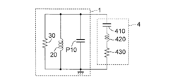
- FIG. 2 is a diagram showing an electrical equivalent circuit of a vibrating body 4 and a vibration control device 1;
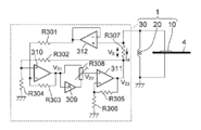
- FIG. 2 is a block diagram showing a configuration example of a resistance circuit 30 included in the vibration control device 1.
- FIG. 6 is a view showing an example of the vibration of the vibrating body 4; It is a figure for demonstrating the effect of this embodiment. It is a figure for demonstrating the effect of this embodiment. It is a figure for demonstrating the effect of this embodiment. It is a figure for demonstrating the effect of this embodiment. It is a figure for demonstrating the effect of this embodiment. It is a figure which shows the structural example of 20 L of pseudo
- FIG. 1 is a block diagram showing a configuration example of a vibration control device 1 according to an embodiment of the present invention.
- a vibrating body 4 to be subjected to vibration control by the vibration control device 1 is illustrated by a dotted line.
- the vibration control device 1 includes a piezo element 10, an inductor 20, and a resistance circuit 30.
- the piezo element 10 is fixed to the vibrator 4.
- the vibrating body 4 is a speaker housing
- the piezo element 10 is fixed to the surface of the speaker housing.
- the distortion of the vibrating body 4 in the state where the natural vibration is generated in the vibrating body 4 is the whole of the vibrating body 4 (in the vibrating body 4, it may mean only a member to which the piezoelectric element 10 is fixed). It is preferable to be fixed to a point larger than the average in the above, and it is more preferable to be fixed to a point that is the largest.
- One of the two electrodes of the piezoelectric element 10 is grounded, and its potential is a reference potential (GND).
- the inductor 20 and the resistance circuit 30 are connected in parallel to the piezo element 10. More specifically, the inductor 20 is provided between one of the two electrodes of the piezoelectric element 10 and the other electrode, and the resistance circuit 30 is also of the two electrodes of the piezoelectric element 10. It is provided between one electrode and the other electrode.
- the resistor circuit 30 is a variable resistor circuit capable of changing the resistance value from a negative value to a positive value.
- FIG. 2 is a view showing an example of the configuration of an electrical equivalent circuit of the entire system including the vibration control device 1 and the vibrating body 4.
- symbol P10 represents the parasitic capacitor of the piezo element 10 in FIG.
- the vibrating body 4 is represented by an electrical equivalent circuit in which the capacitor 410, the inductor 420, and the resistor 430 are connected in series.
- the capacitance Cm of the capacitor 410 in this electrical equivalent circuit is a parameter representing the rigidity of the natural vibration of the vibrating body 4.
- the inductance Lm of the inductor 420 is a parameter representing the mass of the natural vibration of the vibrating body 4, and the resistance value Res of the resistor 430 is a parameter representing the damping of the natural vibration of the vibrating body 4.
- the vibration of the vibrator 4 is characterized by the parameters of the capacitance Cm, the inductance Lm and the resistance value Res. Specifically, the resonance frequency (1 / (2 ⁇ (Lm ⁇ Cm))) of the electric equivalent circuit coincides with the frequency of the natural vibration of the vibrating body 4.
- ⁇ is the circle ratio
- ⁇ (Lm ⁇ Cm) is the square root of Lm ⁇ Cm.
- the resistor 430 acts to damp the vibrational energy of the vibrator 4. Therefore, if the resistance value of the resistor 430 can be increased or decreased, it is possible to extend or shorten the vibration continuation time.
- the combined resistance of the resistor 430 and the resistor circuit 30 acts to attenuate the vibration energy of the vibrating body 4.
- the resistance value Rn of the resistor circuit 30 is a positive value
- the resistance value (Rn + Res) of the combined resistor is larger than the resistance value Res of the resistor 430.
- Q of series resonance due to the inductor 420 and the capacitor 410 is lowered, and a damping action is obtained.
- the inductor 20 is inserted to prevent the series resonance current of the capacitor 410 and the inductor 420 from flowing in the path of the parasitic capacitor P10 of the piezoelectric element 10 at the resonance frequency by utilizing the parallel resonance action with the parasitic capacitor P10 of the piezoelectric element 10 It is done.
- the inductance of the inductor 20 is set such that the resonant frequency of the parallel resonant circuit formed of the inductor 20 and the parasitic capacitor P10 substantially matches the resonant frequency of the series resonant circuit which is the electrical equivalent circuit of the vibrating body 4 .
- the resonant frequency of the vibrating body 4 is obtained by actually vibrating the vibrating body 4 and detecting a frequency at which the amplitude of the vibration is substantially maximized.
- the capacitance of the parasitic capacitor P10 of the piezoelectric element 10 may be obtained by measuring the capacitance value (capacitance) of the piezoelectric element 10 alone.
- FIG. 3 is a view showing a configuration example of the resistance circuit 30.
- an inductor 20 and a piezo element 10 which constitute the vibration control device 1 together with the resistance circuit 30, and a vibrator 4 whose vibration is controlled by the vibration control device 1 are illustrated.
- the resistor circuit 30 includes resistors R301 to R307, a semi-fixed resistor R308, an amplifier 309, operational amplifiers 310 and 311, and a voltage follower 312.
- the resistor R307 is a current detection resistor that detects the above-described series resonance current.
- the first end of the resistor R307 is connected to the non-grounded electrode of the piezo element 10, and the first end is connected to the inverting input terminal of the operational amplifier 310 via the voltage follower 312 and the resistor R301.
- the voltage follower 312 is a buffer amplifier configured by an operational amplifier, and is an impedance conversion circuit having a high input impedance and a low output impedance. When the resistance value of the resistor R301 is sufficiently larger than the resistance value of the resistor R307, the voltage follower 312 may be omitted.
- the second end of the resistor R307 is connected to the noninverting input terminal of the operational amplifier 310 via the resistor R302, and the noninverting input terminal of the operational amplifier 310 is grounded via the resistor R304.
- the output terminal of the operational amplifier 310 is connected to the inverting input terminal via a resistor R303.
- the voltage across the resistor R 307 is input to the operational amplifier 310, and the operational amplifier 310 converts the voltage into a single-ended signal based on the reference potential (GND) and outputs it.
- the output terminal of the operational amplifier 310 is connected to one of the two fixed electrodes of the half fixed resistor R 308 and is connected to the other fixed electrode of the half fixed resistor R 308 via the amplifier 309.
- the amplifier 309 outputs a signal obtained by inverting the output signal of the operational amplifier 310 by A times.
- the movable electrode of the half fixed resistor R ⁇ b> 308 is connected to the non-inverted input terminal of the operational amplifier 311.
- the resistance r from the fixed electrode on the side connected to the output terminal of the amplifier 309 in the half fixed resistor R308 to the movable electrode is It varies continuously from 0 to R8 (R8> 0) depending on the position.
- the semi-fixed resistor R308 divides the voltage applied between the fixed electrodes into r: (R8-r) according to the position of the movable electrode, and outputs the divided voltage to the non-inverting input terminal of the operational amplifier 311.
- the inverting input terminal of the operational amplifier 311 is grounded via the resistor R306.
- the output terminal of the operational amplifier 311 is connected to the terminal (the second end of the resistor R307) on the side connected to the resistor R302 of the resistor R307, and also connected to the inverting input terminal of the operational amplifier 311 via the resistor R305. .
- the current flowing through the resistor R307 is Ix
- the voltage across the resistor R307 is Vx
- the output voltage of the operational amplifier 310 is Vz1
- the voltage of the movable electrode of the half fixed resistor R308 is Vz2
- the output of the operational amplifier 311 Voltage of Vz3
- resistances of resistors R301 to R306, resistances of R1 to R6, resistance of resistor R307 to Rd the gain of an amplifier consisting of resistors R301 to R304 and op amp 310
- A1 of an amplifier consisting of resistors R305 and R306 and op amp 311 Assuming that the gain is A2, there is a relationship shown in the following formulas (1) to (6).
- A1 R4 / (R2 + R4) ⁇ ⁇ (R3 / R1) +1 ⁇ (1)
- A2 ((R5 / R6) +1) (2)
- Vx Rd ⁇ Ix (3)
- Vz1 Vx (-A1) (4)
- Vz2 ⁇ (R8-r) -r.A ⁇ .Vz1 / R8 (5)
- Vz3 Vz2 ⁇ A2 (6)
- the resistance value Rn of the resistance circuit 3 can be expressed as the following equation (11).
- Rn (Vx ⁇ Ix ⁇ Rd ⁇ A0)
- Ix V x / I x-R d ⁇ A 0 (11)
- the resistance value Rn of the resistor circuit 30 is expressed as the following equation (12).
- the resistance value Rn of the resistance circuit 30 is determined according to the resistance values R1 to R6 of the resistors R301 to R306, the resistance value r of the half fixed resistor R308, and the gain A of the amplifier 309, and when A0> 1, that is, It becomes a negative value when (1 + A) ⁇ r ⁇ 1-1 / (A1 ⁇ A2) ⁇ ⁇ R8.
- the resistance value Rn of the resistance circuit 30 can be adjusted by adjusting the resistance value r of the semifixed resistor R308. It can be varied continuously from negative values to positive values.
- the above is the configuration of the vibration control device.
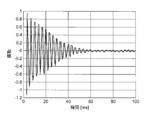
- FIG. 4 is a diagram showing a time change of vibration of the vibrating body 4 when the vibration control by the vibration control device 1 is not performed.
- FIG. 5 is a diagram showing the time change of the vibration of the vibrating body 4 when the vibration control by the vibration control device 1 is performed with the resistance value Rn of the resistance circuit 30 set to a positive value, and
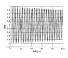
- FIG. It is a figure which shows the time change of a vibration of the vibrating body 4 at the time of performing vibration control by the vibration control apparatus 1 by setting resistance value Rn of the circuit 30 to a negative value.
- the vibration control of the vibrating body 4 can be performed by setting the resistance value Rn of the resistance circuit 30 to a positive value.
- the vibration body 4 can be excited by setting the value Rn to a negative value.
- the resistance circuit 30 may be a variable resistance circuit capable of changing the resistance value in the range of negative values.
- the resistance circuit 30 may be a variable resistance circuit capable of changing the resistance value in the positive value range.
- the resistance circuit 30 does not have to be a variable resistance, as long as a suitable value of the resistance value of the resistance circuit 30 is known in advance for damping or exciting the vibrating body 4.
- the pseudo inductor circuit 20A shown in FIG. 8 may be used as the inductor 20.
- the pseudo inductor circuit 20A includes a first current feedback amplifier circuit 21, a second current feedback amplifier circuit 22, and a voltage follower 23 which is a buffer amplifier composed of an operational amplifier, and an integration. And a circuit 24.
- the value of the inductance may be adjusted to match the resonant frequency of the parallel resonant circuit composed of the inductor 20 and the parasitic capacitor P10 with the resonant frequency of the vibrating body 4 it can.
- the voltage follower 23 is an impedance conversion circuit having a high input impedance and a low output impedance, amplifies the voltage of the processing node P1 to which the ungrounded electrode of the piezoelectric element 10 is connected with a gain 1 and outputs it. .
- the integrating circuit 24 is configured of a variable resistor R205, an operational amplifier 206, and an integrating capacitor Ca.
- the variable resistor R 205 is interposed between the output terminal of the voltage follower 23 and the inverting input terminal of the operational amplifier 206.
- the noninverting input terminal of the operational amplifier 206 is grounded.
- an integration capacitor Ca is inserted between the output terminal of the operational amplifier 206 and the inverting input terminal.
- the integration capacitor Ca is charged with a current obtained by dividing the output voltage of the voltage follower 23 by the resistance value of the variable resistor R205.
- a voltage obtained by integrating the output voltage of the voltage follower 23 that is, the voltage of the processing node P1 is output from the operational amplifier 206.
- the first current feedback amplifier circuit 21 includes resistors R201 and R203, a PNP transistor Tp, and a DC power supply Vb1.
- the resistor R201 is inserted between the positive power supply Vcc and the emitter of the PNP transistor Tp.
- the resistor R203 is inserted between the output terminal of the operational amplifier 206 (that is, the output terminal of the integration circuit 24) and the emitter of the PNP transistor Tp.
- the collector of the PNP transistor Tp is connected to the processing node P1.
- the power supply Vb1 applies a forward bias between the base and the emitter of the PNP transistor Tp by applying to the base of the PNP transistor Tp a potential lower than the potential of the positive power supply Vcc by a predetermined voltage.
- the current passing from the positive power supply Vcc to the resistor R201 is shunted to the PNP transistor Tp and the resistor R203.
- the output voltage of the integration circuit 24 rises, the current flowing to the resistor R203 decreases, and the emitter current flowing to the PNP transistor Tp increases by an amount corresponding to the decrease.
- the output voltage of the integrating circuit 24 decreases, the current flowing to the resistor R203 increases, and the emitter current flowing to the PNP transistor Tp decreases by an amount corresponding to the increase.
- the second current feedback type amplifier circuit 22 includes resistors R202 and R204, an NPN transistor Tn, and a DC power supply Vb2.
- the resistor R202 is inserted between the negative power supply Vee and the emitter of the NPN transistor Tn.
- the resistor R 204 is inserted between the output terminal of the integrating circuit 24 and the emitter of the NPN transistor Tn.
- the collector of the NPN transistor Tn is connected to the processing node P1.
- the power supply Vb2 applies a forward bias between the base and the emitter of the NPN transistor Tn by applying a potential higher by a predetermined voltage than the potential of the negative power supply Vee to the base of the NPN transistor Tn.
- the emitter current of the NPN transistor Tn and the current supplied from the integrating circuit 24 via the resistor R204 flow into the negative power supply Vee via the resistor R202.
- the output voltage of the integration circuit 24 rises, the current flowing to the resistor R 204 increases, and the emitter current flowing to the NPN transistor Tn decreases by that amount.
- the output voltage of the integration circuit 24 decreases, the current flowing to the resistor R 204 decreases, and the emitter current flowing to the NPN transistor Tn increases by the amount corresponding to the decrease.
- the above is the configuration of the pseudo inductor circuit 20A.
- This ⁇ i1 is a current which is negatively fed back to the processing node P1 via the current feedback type amplifier circuits 21 and 22 when the voltage of the processing node P1 fluctuates by ⁇ v1, and this current ⁇ i1 is a processing node P1.
- the application object of the present invention is not limited to the vibration control of the vibrator.
- the present invention is applicable to the measurement of the parameters Lm, Cm and Res characterizing the natural vibration of the vibrating body when the vibrating body is replaced by an electrical equivalent circuit (series resonant circuit in FIG. 2). .
- FIG. 9 is a flow chart showing the flow of the method of measuring electrical equivalent circuit parameters according to the present invention.
- a measurer who measures the parameters Lm, Cm, and Res according to the measurement method first fixes a piezo element to a vibrating body, and connects an inductor to the piezo element in parallel (step SA100).
- the reason why the inductor is connected in parallel to the piezoelectric element is to prevent current from flowing in the parasitic capacitor of the piezoelectric element at the resonance frequency when the vibrator is replaced with the electrical equivalent circuit.
- a parallel resonance circuit is configured by an inductor connected in parallel to a parasitic capacitor of a piezo element, and the resonance frequency of this parallel resonance circuit is made to substantially coincide with the resonance frequency of the vibrating body to prevent current from flowing to the parasitic capacitor. be able to.
- the resonant frequency of the vibrating body can be obtained by measuring the frequency at which the vibration amplitude is substantially maximized by vibrating the vibrating body.
- the capacitance of the piezo element can be obtained by measuring the capacitance of the element alone.
- the measurer applies a predetermined impulse vibration to the vibrator to measure the voltage V1 appearing at both ends of the piezoelectric element (step SA110). Then, the measurer connects a resistor in parallel to the inductor, applies an impulse vibration equivalent to the impulse vibration given to the vibrator at step SA110 to the vibrator, and measures a voltage V2 appearing at both ends of the resistor. (Step SA120).
- the reason why the resistance value Res is calculated by the equation (19A) is as follows.
- the voltage V1 measured in step SA110 corresponds to the generated voltage of the piezoelectric element.
- the voltage V2 measured in step SA120 is a voltage obtained by dividing the voltage V1 by the resistor connected to the inductor in step SA120 and the resistor 430.
- V2 V1 ⁇ Rd / (Rd + Res) (19B)
- the measurer applies a predetermined impulse vibration to the vibrator, and measures the frequency response of the voltage appearing at both ends of the resistor connected in parallel to the inductor in step SA120 (step SA140).
- the measurer calculates the Q value of the resonance of the vibrator, that is, the Q value of the resonance due to the capacitance Cm and the inductance Lm, based on the frequency response measured in the above manner (step SA150). More specifically, the measurer first determines from the frequency response measured in step SA140 that, in the frequency range where the voltage turns from increasing to decreasing as the frequency increases, the voltage peaking at the first frequency. Read the frequency (ie, the resonant frequency) wo.
- the second frequency wp1 and the third frequency wp2 (wp1 ⁇ wo ⁇ wp2) at which the voltage is 1 / ⁇ 2 times the voltage at the peak are read in the same frequency range.
- the measurer uses the first frequency wo, the second frequency w1 and the third frequency w2 read from the frequency response to calculate the Q value of the resonance of the vibrator according to the following equation (20).
- Q wo / (wp2-wp1) (20)
- the measurer calculates the capacitance Cm and the inductance Lm using the resistance value Res calculated in step SA130 and the Q value calculated in step SA150 (step SA160). Since the Q value calculated according to equation (20) can also be expressed by the following equation (21) or equation (22), the measurer uses the Q value calculated according to equation (20) in equation (21) The value of Lm can be determined by substituting and solving for Lm. Similarly, the measurer can substitute the Q calculated according to the equation (20) into the equation (22) and solve for Cm to obtain the value of Cm.
- Q wo ⁇ Lm / (Res + Rd) (21)
- Q 1 / (wo ⁇ Cm ⁇ (Res + Rd)) (22)
- the parameters Res, Cm and Lm of the electrical equivalent circuit of the vibrator it is possible to actually measure the parameters Res, Cm and Lm of the electrical equivalent circuit of the vibrator.
- these parameters are calculated by simulation etc., and the inductance etc. of the vibration damping device is determined according to the calculation result, which is one of the reasons why a sufficient vibration damping effect can not be obtained. Met.
- the vibration control device can be applied to various vibrators, and can be applied to, for example, musical instruments as well as the above-described speaker.
- musical instruments include percussion instruments such as marimba, keyboard instruments such as piano, and string instruments such as violin.
Landscapes
- Engineering & Computer Science (AREA)
- Physics & Mathematics (AREA)
- Acoustics & Sound (AREA)
- Mechanical Engineering (AREA)
- General Engineering & Computer Science (AREA)
- Multimedia (AREA)
- Aviation & Aerospace Engineering (AREA)
- Signal Processing (AREA)
- Apparatuses For Generation Of Mechanical Vibrations (AREA)
- Vibration Prevention Devices (AREA)
- Circuit For Audible Band Transducer (AREA)
- General Electrical Machinery Utilizing Piezoelectricity, Electrostriction Or Magnetostriction (AREA)
Applications Claiming Priority (2)
| Application Number | Priority Date | Filing Date | Title |
|---|---|---|---|
| JP2017167341A JP6826323B2 (ja) | 2017-08-31 | 2017-08-31 | 振動制御装置 |
| JP2017-167341 | 2017-08-31 |
Publications (1)
| Publication Number | Publication Date |
|---|---|
| WO2019044070A1 true WO2019044070A1 (ja) | 2019-03-07 |
Family
ID=65527359
Family Applications (1)
| Application Number | Title | Priority Date | Filing Date |
|---|---|---|---|
| PCT/JP2018/020004 Ceased WO2019044070A1 (ja) | 2017-08-31 | 2018-05-24 | 振動制御装置 |
Country Status (2)
| Country | Link |
|---|---|
| JP (1) | JP6826323B2 (enExample) |
| WO (1) | WO2019044070A1 (enExample) |
Citations (3)
| Publication number | Priority date | Publication date | Assignee | Title |
|---|---|---|---|---|
| US5783898A (en) * | 1996-02-26 | 1998-07-21 | Mcdonnell Douglas Corporation | Piezoelectric shunts for simultaneous vibration reduction and damping of multiple vibration modes |
| JP2007071238A (ja) * | 2005-09-05 | 2007-03-22 | Japan Aerospace Exploration Agency | 構造物の制振装置 |
| WO2017150267A1 (ja) * | 2016-03-01 | 2017-09-08 | ヤマハ株式会社 | 振動制御装置 |
Family Cites Families (7)
| Publication number | Priority date | Publication date | Assignee | Title |
|---|---|---|---|---|
| JP2003119719A (ja) * | 2001-10-17 | 2003-04-23 | Ishikawajima Harima Heavy Ind Co Ltd | 鉄橋の騒音低減方法及び装置 |
| US6870303B2 (en) * | 2002-05-08 | 2005-03-22 | Pohang University Of Science And Technology Foundation | Multi-mode vibration damping device and method using negative capacitance shunt circuits |
| JP2004048652A (ja) * | 2002-11-29 | 2004-02-12 | Toyo Commun Equip Co Ltd | 高周波圧電発振器 |
| JP4154261B2 (ja) * | 2003-03-12 | 2008-09-24 | リオン株式会社 | 音響・振動制御装置 |
| JP5023282B2 (ja) * | 2007-04-10 | 2012-09-12 | 英彰 高島 | 圧電発振器 |
| JP2013239779A (ja) * | 2012-05-11 | 2013-11-28 | Asahi Kasei Electronics Co Ltd | 無線装置及びそれを備えたセンサ並びに無線タグ |
| US20140354112A1 (en) * | 2013-05-31 | 2014-12-04 | GM Global Technology Operations LLC | Piezoelectric resonators for reduction of noise and vibration in vehicle components |
-
2017
- 2017-08-31 JP JP2017167341A patent/JP6826323B2/ja active Active
-
2018
- 2018-05-24 WO PCT/JP2018/020004 patent/WO2019044070A1/ja not_active Ceased
Patent Citations (3)
| Publication number | Priority date | Publication date | Assignee | Title |
|---|---|---|---|---|
| US5783898A (en) * | 1996-02-26 | 1998-07-21 | Mcdonnell Douglas Corporation | Piezoelectric shunts for simultaneous vibration reduction and damping of multiple vibration modes |
| JP2007071238A (ja) * | 2005-09-05 | 2007-03-22 | Japan Aerospace Exploration Agency | 構造物の制振装置 |
| WO2017150267A1 (ja) * | 2016-03-01 | 2017-09-08 | ヤマハ株式会社 | 振動制御装置 |
Also Published As
| Publication number | Publication date |
|---|---|
| JP6826323B2 (ja) | 2021-02-03 |
| JP2019047271A (ja) | 2019-03-22 |
Similar Documents
| Publication | Publication Date | Title |
|---|---|---|
| US8752416B2 (en) | Resonant conductor measurement system and method | |
| KR100341964B1 (ko) | 물리 변수 검출장치 및 방법 | |
| JP5010006B2 (ja) | モーショナルフィードバックシステム | |
| JP2018028473A5 (enExample) | ||
| JP6862731B2 (ja) | 制振装置 | |
| WO2019044070A1 (ja) | 振動制御装置 | |
| JP2012156946A (ja) | 発振回路およびそれを用いた振動式センサ | |
| JP2015132570A (ja) | 粘度測定装置及び粘度測定方法 | |
| CN100432682C (zh) | 电位固定装置及电位固定方法 | |
| JP5371505B2 (ja) | 温度補償回路ならびに加速度または角速度センサ | |
| JP2007057262A (ja) | センサ回路 | |
| Maillou et al. | Modelling nonlinear viscoelastic behaviours of loudspeaker suspensions-like structures | |
| JP2012052862A (ja) | 試験装置用の電源装置およびそれを用いた試験装置 | |
| JP2006197206A (ja) | スピーカ装置 | |
| Byju et al. | An enhanced voltage amplifier scheme insensitive to cable parasitic capacitance for interfacing piezoelectric sensors | |
| Boutin et al. | Modifying the resonances of a xylophone bar using active control | |
| JP2017098817A (ja) | 駆動装置 | |
| JP4406863B2 (ja) | 振動型角速度センサ装置 | |
| EP1606971A1 (en) | Loudspeaker equipped with measurement of the movement of the loudspeaker unit and a method for measuring the movement of the loudspeaker unit in a loudspeaker | |
| JP4676643B2 (ja) | 電位固定装置および容量測定装置 | |
| WO2021120387A1 (zh) | 材料动态测量方法和轴向振动测量系统 | |
| US11701687B2 (en) | Drive circuit, transducer system, and inspection device | |
| SU1408238A1 (ru) | Устройство дл бесконтактного измерени параметров вибрации | |
| Sørensen et al. | Material models in loudspeakers using frictional elements | |
| JPH0949736A (ja) | 振動型ジャイロスコープの駆動装置 |
Legal Events
| Date | Code | Title | Description |
|---|---|---|---|
| 121 | Ep: the epo has been informed by wipo that ep was designated in this application |
Ref document number: 18851941 Country of ref document: EP Kind code of ref document: A1 |
|
| NENP | Non-entry into the national phase |
Ref country code: DE |
|
| 122 | Ep: pct application non-entry in european phase |
Ref document number: 18851941 Country of ref document: EP Kind code of ref document: A1 |