WO2019031579A1 - 表示装置 - Google Patents
表示装置 Download PDFInfo
- Publication number
- WO2019031579A1 WO2019031579A1 PCT/JP2018/029905 JP2018029905W WO2019031579A1 WO 2019031579 A1 WO2019031579 A1 WO 2019031579A1 JP 2018029905 W JP2018029905 W JP 2018029905W WO 2019031579 A1 WO2019031579 A1 WO 2019031579A1
- Authority
- WO
- WIPO (PCT)
- Prior art keywords
- insulating layer
- layer
- detection electrode
- inorganic insulating
- terminal
- Prior art date
- Legal status (The legal status is an assumption and is not a legal conclusion. Google has not performed a legal analysis and makes no representation as to the accuracy of the status listed.)
- Ceased
Links
Images


Classifications
-
- G—PHYSICS
- G06—COMPUTING OR CALCULATING; COUNTING
- G06F—ELECTRIC DIGITAL DATA PROCESSING
- G06F3/00—Input arrangements for transferring data to be processed into a form capable of being handled by the computer; Output arrangements for transferring data from processing unit to output unit, e.g. interface arrangements
- G06F3/01—Input arrangements or combined input and output arrangements for interaction between user and computer
- G06F3/03—Arrangements for converting the position or the displacement of a member into a coded form
- G06F3/041—Digitisers, e.g. for touch screens or touch pads, characterised by the transducing means
- G06F3/044—Digitisers, e.g. for touch screens or touch pads, characterised by the transducing means by capacitive means
- G06F3/0445—Digitisers, e.g. for touch screens or touch pads, characterised by the transducing means by capacitive means using two or more layers of sensing electrodes, e.g. using two layers of electrodes separated by a dielectric layer
-
- G—PHYSICS
- G06—COMPUTING OR CALCULATING; COUNTING
- G06F—ELECTRIC DIGITAL DATA PROCESSING
- G06F3/00—Input arrangements for transferring data to be processed into a form capable of being handled by the computer; Output arrangements for transferring data from processing unit to output unit, e.g. interface arrangements
- G06F3/01—Input arrangements or combined input and output arrangements for interaction between user and computer
- G06F3/03—Arrangements for converting the position or the displacement of a member into a coded form
- G06F3/041—Digitisers, e.g. for touch screens or touch pads, characterised by the transducing means
- G06F3/0412—Digitisers structurally integrated in a display
-
- G—PHYSICS
- G06—COMPUTING OR CALCULATING; COUNTING
- G06F—ELECTRIC DIGITAL DATA PROCESSING
- G06F3/00—Input arrangements for transferring data to be processed into a form capable of being handled by the computer; Output arrangements for transferring data from processing unit to output unit, e.g. interface arrangements
- G06F3/01—Input arrangements or combined input and output arrangements for interaction between user and computer
- G06F3/03—Arrangements for converting the position or the displacement of a member into a coded form
- G06F3/041—Digitisers, e.g. for touch screens or touch pads, characterised by the transducing means
- G06F3/0416—Control or interface arrangements specially adapted for digitisers
- G06F3/04164—Connections between sensors and controllers, e.g. routing lines between electrodes and connection pads
-
- G—PHYSICS
- G06—COMPUTING OR CALCULATING; COUNTING
- G06F—ELECTRIC DIGITAL DATA PROCESSING
- G06F3/00—Input arrangements for transferring data to be processed into a form capable of being handled by the computer; Output arrangements for transferring data from processing unit to output unit, e.g. interface arrangements
- G06F3/01—Input arrangements or combined input and output arrangements for interaction between user and computer
- G06F3/03—Arrangements for converting the position or the displacement of a member into a coded form
- G06F3/041—Digitisers, e.g. for touch screens or touch pads, characterised by the transducing means
- G06F3/044—Digitisers, e.g. for touch screens or touch pads, characterised by the transducing means by capacitive means
- G06F3/0446—Digitisers, e.g. for touch screens or touch pads, characterised by the transducing means by capacitive means using a grid-like structure of electrodes in at least two directions, e.g. using row and column electrodes
-
- G—PHYSICS
- G09—EDUCATION; CRYPTOGRAPHY; DISPLAY; ADVERTISING; SEALS
- G09F—DISPLAYING; ADVERTISING; SIGNS; LABELS OR NAME-PLATES; SEALS
- G09F9/00—Indicating arrangements for variable information in which the information is built-up on a support by selection or combination of individual elements
- G09F9/30—Indicating arrangements for variable information in which the information is built-up on a support by selection or combination of individual elements in which the desired character or characters are formed by combining individual elements
-
- H—ELECTRICITY
- H05—ELECTRIC TECHNIQUES NOT OTHERWISE PROVIDED FOR
- H05B—ELECTRIC HEATING; ELECTRIC LIGHT SOURCES NOT OTHERWISE PROVIDED FOR; CIRCUIT ARRANGEMENTS FOR ELECTRIC LIGHT SOURCES, IN GENERAL
- H05B33/00—Electroluminescent light sources
- H05B33/02—Details
- H05B33/04—Sealing arrangements, e.g. against humidity
-
- H—ELECTRICITY
- H05—ELECTRIC TECHNIQUES NOT OTHERWISE PROVIDED FOR
- H05B—ELECTRIC HEATING; ELECTRIC LIGHT SOURCES NOT OTHERWISE PROVIDED FOR; CIRCUIT ARRANGEMENTS FOR ELECTRIC LIGHT SOURCES, IN GENERAL
- H05B33/00—Electroluminescent light sources
- H05B33/02—Details
- H05B33/06—Electrode terminals
-
- H—ELECTRICITY
- H05—ELECTRIC TECHNIQUES NOT OTHERWISE PROVIDED FOR
- H05B—ELECTRIC HEATING; ELECTRIC LIGHT SOURCES NOT OTHERWISE PROVIDED FOR; CIRCUIT ARRANGEMENTS FOR ELECTRIC LIGHT SOURCES, IN GENERAL
- H05B33/00—Electroluminescent light sources
- H05B33/10—Apparatus or processes specially adapted to the manufacture of electroluminescent light sources
-
- H—ELECTRICITY
- H05—ELECTRIC TECHNIQUES NOT OTHERWISE PROVIDED FOR
- H05B—ELECTRIC HEATING; ELECTRIC LIGHT SOURCES NOT OTHERWISE PROVIDED FOR; CIRCUIT ARRANGEMENTS FOR ELECTRIC LIGHT SOURCES, IN GENERAL
- H05B33/00—Electroluminescent light sources
- H05B33/12—Light sources with substantially two-dimensional [2D] radiating surfaces
- H05B33/22—Light sources with substantially two-dimensional [2D] radiating surfaces characterised by the chemical or physical composition or the arrangement of auxiliary dielectric or reflective layers
-
- H—ELECTRICITY
- H10—SEMICONDUCTOR DEVICES; ELECTRIC SOLID-STATE DEVICES NOT OTHERWISE PROVIDED FOR
- H10K—ORGANIC ELECTRIC SOLID-STATE DEVICES
- H10K50/00—Organic light-emitting devices
- H10K50/80—Constructional details
- H10K50/84—Passivation; Containers; Encapsulations
- H10K50/844—Encapsulations
-
- H—ELECTRICITY
- H10—SEMICONDUCTOR DEVICES; ELECTRIC SOLID-STATE DEVICES NOT OTHERWISE PROVIDED FOR
- H10K—ORGANIC ELECTRIC SOLID-STATE DEVICES
- H10K59/00—Integrated devices, or assemblies of multiple devices, comprising at least one organic light-emitting element covered by group H10K50/00
- H10K59/10—OLED displays
- H10K59/12—Active-matrix OLED [AMOLED] displays
- H10K59/131—Interconnections, e.g. wiring lines or terminals
-
- H—ELECTRICITY
- H10—SEMICONDUCTOR DEVICES; ELECTRIC SOLID-STATE DEVICES NOT OTHERWISE PROVIDED FOR
- H10K—ORGANIC ELECTRIC SOLID-STATE DEVICES
- H10K59/00—Integrated devices, or assemblies of multiple devices, comprising at least one organic light-emitting element covered by group H10K50/00
- H10K59/40—OLEDs integrated with touch screens
-
- H—ELECTRICITY
- H10—SEMICONDUCTOR DEVICES; ELECTRIC SOLID-STATE DEVICES NOT OTHERWISE PROVIDED FOR
- H10K—ORGANIC ELECTRIC SOLID-STATE DEVICES
- H10K59/00—Integrated devices, or assemblies of multiple devices, comprising at least one organic light-emitting element covered by group H10K50/00
- H10K59/80—Constructional details
- H10K59/87—Passivation; Containers; Encapsulations
- H10K59/873—Encapsulations
- H10K59/8731—Encapsulations multilayered coatings having a repetitive structure, e.g. having multiple organic-inorganic bilayers
-
- G—PHYSICS
- G06—COMPUTING OR CALCULATING; COUNTING
- G06F—ELECTRIC DIGITAL DATA PROCESSING
- G06F2203/00—Indexing scheme relating to G06F3/00 - G06F3/048
- G06F2203/041—Indexing scheme relating to G06F3/041 - G06F3/045
- G06F2203/04103—Manufacturing, i.e. details related to manufacturing processes specially suited for touch sensitive devices
-
- G—PHYSICS
- G06—COMPUTING OR CALCULATING; COUNTING
- G06F—ELECTRIC DIGITAL DATA PROCESSING
- G06F2203/00—Indexing scheme relating to G06F3/00 - G06F3/048
- G06F2203/041—Indexing scheme relating to G06F3/041 - G06F3/045
- G06F2203/04112—Electrode mesh in capacitive digitiser: electrode for touch sensing is formed of a mesh of very fine, normally metallic, interconnected lines that are almost invisible to see. This provides a quite large but transparent electrode surface, without need for ITO or similar transparent conductive material
-
- H—ELECTRICITY
- H10—SEMICONDUCTOR DEVICES; ELECTRIC SOLID-STATE DEVICES NOT OTHERWISE PROVIDED FOR
- H10K—ORGANIC ELECTRIC SOLID-STATE DEVICES
- H10K71/00—Manufacture or treatment specially adapted for the organic devices covered by this subclass
Definitions
- One embodiment of the present invention relates to a display device having an input function.
- One embodiment of the invention disclosed herein relates to a wiring structure of a display device in which a touch sensor is incorporated.
- a display panel used for such an electronic device is also called a touch panel (or touch screen).
- a capacitive touch sensor is adopted.
- capacitive touch sensors there is one that detects a change in electrostatic capacitance between a pair of sensor electrodes, which is also called a Tx electrode and an Rx electrode, as an input signal.
- the conventional touch panel has a structure in which a touch sensor panel and a display panel are superimposed.
- the problem is that the thickness of the display increases.
- a structure in which a touch sensor panel and a display panel are superimposed is a factor that hinders flexibility.
- the structure which built in the function of the touch sensor in the display panel is disclosed.
- a display panel using an organic electroluminescent element hereinafter, also referred to as "organic EL element”
- the first detection electrode and the second detection electrode are disposed with an inorganic insulating film provided as a sealing film interposed therebetween.
- an in-cell type in which a touch sensor is provided in a panel is disclosed (see Patent Document 1).
- the wiring connected with a detection electrode will be needed and the number of wiring layers will increase.
- the display panel needs to protect the display element with the sealing layer, so a process of forming a detection electrode and a wiring or a wiring connected to the detection electrode and a terminal electrode It is necessary to provide a connection structure without deteriorating the sealing performance of the sealing layer.
- a substrate having an insulating surface, a pixel portion in which a plurality of pixels arranged on the insulating surface are arrayed, and a region disposed on the insulating surface in an area outside the pixel portion
- a terminal portion including one terminal and a second terminal disposed in a region inside the first terminal, a wiring portion including a first wiring disposed between the pixel portion and the terminal portion, and a pixel portion overlapping
- the sealing portion covering the pixel portion and the wiring portion, and the sealing portion includes the first inorganic insulating layer, the organic insulating layer, and the second inorganic insulating layer in this order from the substrate side.
- the organic insulating layer is disposed in a region overlapping the pixel portion, the first inorganic insulating layer and the second inorganic insulating layer are disposed in a region overlapping the pixel portion and the wiring portion, and the sensing portion is formed of the first inorganic insulating layer
- a first detection electrode disposed on the upper layer side and lower than the second inorganic insulating layer
- a second detection electrode disposed on the upper layer side of the insulating layer, and the first wiring included in the wiring portion is electrically connected to the first detection electrode at an opening provided in the second inorganic insulating layer
- the first wiring extends to the outer region of the second inorganic insulating layer and is electrically connected to the second terminal.
- a pixel portion in which a plurality of pixels are arrayed is formed on a substrate having an insulating surface, and a terminal including a first terminal in an area outside the pixel portion on the insulating surface.
- a first detection electrode layer is formed, an organic insulating layer covering the first detection electrode layer is formed, a second inorganic insulating layer covering the organic insulating layer is formed, and a first inorganic insulating layer and a second on the second terminal are formed.
- a second detection electrode layer which forms an opening for exposing the first detection electrode layer in the second insulating layer while removing the inorganic insulating layer, and extends in a direction intersecting the first direction on the second inorganic insulating layer.
- a first wiring connected to the second terminal, the opening provided in the second inorganic insulating layer Forming a first wiring connected to the first detection electrode are.
- FIG. 4 is a cross-sectional view taken along line X1-X2 of FIG. 3 showing a configuration of a display device according to an embodiment of the present invention. It is a sectional view showing composition of a pixel field of a display concerning one embodiment of the present invention.
- FIG. 6 shows a flowchart illustrating a method of manufacturing a display device according to an embodiment of the present invention. It is a top view which shows the structure of the peripheral region of the display apparatus which concerns on other embodiment of this invention. It is sectional drawing which shows the structure of the display apparatus which concerns on other embodiment of this invention. It is a top view which shows the structure of the peripheral region of the display apparatus based on other embodiment of this invention. It is sectional drawing which shows the structure of the display apparatus which concerns on further another embodiment of this invention.
- FIG. 7 is a cross-sectional view showing the manufacturing process of the display device according to the embodiment of the present invention. FIG. 7 is a cross-sectional view showing the manufacturing process of the display device according to the embodiment of the present invention. FIG. 7 is a cross-sectional view showing the manufacturing process of the display device according to the embodiment of the present invention.
- FIG. 7 is a cross-sectional view showing the manufacturing process of the display device according to the embodiment of the present invention.
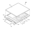
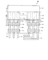
- FIG. 1 is a perspective view showing a display device 100 according to an embodiment of the present invention.
- the pixel portion 104 and the touch sensor 108 are provided on one main surface of a substrate 102 having an insulating surface.
- a plurality of pixels 106 are arranged in the pixel unit 104.
- the plurality of pixels 106 are arranged in, for example, the row direction and the column direction in the pixel unit 104.
- the touch sensor 108 is disposed to overlap the pixel portion 104. In other words, the touch sensor 108 is disposed so as to overlap with the plurality of pixels 106.
- a plurality of detection electrodes 107 are arranged in a matrix, and each is connected in the row direction or the column direction.
- the pixel 106 and the touch sensor 108 are schematically represented, and the magnitude relationship thereof is not limited to that shown in FIG.
- the display device 100 includes a first terminal area 112a to which a video signal or the like is input, and a second terminal area 112b to which signals of the touch sensor 108 are input / output.
- the first terminal region 112 a and the second terminal region 112 b are disposed at one end of one main surface of the substrate 102 having an insulating surface.
- a plurality of terminal electrodes are arranged along the end of the substrate 102 having the insulating surface.
- the plurality of terminal electrodes of the first terminal area 112 a and the second terminal area 112 b are connected to the flexible printed wiring board 114.
- the driver circuit 110 outputs a video signal to the pixel 106.
- the drive circuit 110 is attached to one main surface of the substrate 102 or the flexible printed wiring board 114.
- the substrate 102 having an insulating surface is made of a member such as glass or plastic (polycarbonate, polyethylene terephthalate, polyimide, polyacrylate or the like).
- plastic polycarbonate, polyethylene terephthalate, polyimide, polyacrylate or the like.
- a polarizing plate 116 including a polarizer may be provided on the pixel portion 104 and the touch sensor 108.
- the polarizing plate 116 is configured of a polarizer exhibiting circular polarization.
- the polarizing plate 116 is formed of a film substrate containing a polarizer.
- the pixel 106 includes a display element and a circuit element.
- the touch sensor 108 is preferably an electrostatic capacitance type, and in the touch sensor 108, a sensing unit is configured by the first detection electrode (Tx wiring) and the second detection electrode (Rx wiring).
- An interlayer insulating layer is provided between the pixel portion 104 and the touch sensor 108 and arranged so as not to electrically short each other.
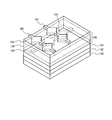
- FIG. 2 is a perspective view showing the configuration of the pixel portion 104 and the touch sensor 108 disposed thereon.
- the pixel portion 104 includes a circuit element layer 122 in which circuit elements are provided on a substrate 102 and a display element layer 124 in which a display element is provided.
- a sealing layer 126 including a detection electrode for the touch sensor is provided on the display element layer 124. The sealing layer 126 is provided so as to cover the upper surface of the pixel region when the main surface on the viewer side is up.
- Circuit element layer 122 includes an interlayer insulating layer.
- the interlayer insulating layer insulates wirings provided in different layers.
- the interlayer insulating layer includes at least one inorganic interlayer insulating layer and at least one organic interlayer insulating layer.
- the inorganic interlayer insulating layer is formed of an inorganic insulating material such as silicon oxide, silicon nitride, silicon oxynitride, or aluminum oxide.
- the organic interlayer insulating layer is formed of an organic insulating material such as acryl or polyimide.
- the circuit element layer 122 includes an active element such as a transistor, a passive element such as a capacitor and a resistor, and a wiring connecting these elements, and is provided so as to be embedded in the interlayer insulating layer.
- the display element layer 124 a light-emitting element or an electro-optical element that exhibits an electro-optical effect by application of a voltage is used as a display element.
- the display element layer 124 includes a pair of electrodes distinguished as an anode and a cathode, an organic layer containing an organic EL material, and an insulating partition layer separating adjacent organic EL elements. It is comprised including.
- the organic EL element is electrically connected to the transistor of the circuit element layer 122.
- the sealing layer 126 has a structure in which a plurality of insulating films are stacked.
- FIG. 2 has a structure in which a first inorganic insulating layer 128, an organic insulating layer 130, and a second inorganic insulating layer 132 are stacked as the sealing layer 126.
- the sealing layer 126 improves sealing performance by a laminated structure in which different materials are combined. For example, even if the first inorganic insulating layer 128 includes a defect, the organic insulating layer 130 burys the defective portion, and the second inorganic insulating layer 132 is further provided to compensate for deterioration in sealing performance due to the defect.
- the second inorganic insulating layer 132 may be provided to cover the entire surface of the pixel portion 104 and at least a part of the region outside the pixel portion 104, and the first inorganic insulating layer 128 and the second inorganic insulating layer 132 may be provided. May be formed to cover a further outside region of the second inorganic insulating layer 132.
- the outer peripheral end portions of the first inorganic insulating layer 128 and the second inorganic insulating layer 132 may not necessarily coincide with each other.
- the first detection electrode 134 and the second detection electrode 140 constituting the sensing unit of the touch sensor 108 the first detection electrode 134 is included in the sealing layer 126, and the second detection electrode 140 is on the upper side of the sealing layer 126. Be placed. Although not shown in FIG. 2, the upper surface of the second detection electrode 140 may be covered with the overcoat layer 184.
- the first detection electrode 134 is disposed to extend in a first direction
- the second detection electrode 140 is disposed to extend in a second direction intersecting the first direction.
- the first direction may be any direction, but may be, for example, a direction along the column direction corresponding to the arrangement of pixels.
- the second direction may be a direction along the arrangement of the pixels in the row direction.
- a plurality of first detection electrodes 134 and a plurality of second detection electrodes 140 are disposed.
- a group of the plurality of first detection electrodes 134 is also referred to as a first detection electrode pattern
- a group of the plurality of second detection electrodes 140 is also referred to as a second detection electrode pattern.
- FIG. 2 only a part of the first detection electrode 134 and the second detection electrode 140 is shown, and a plurality of these detection electrodes are arranged along substantially the entire pixel portion 104. Ru.
- the first detection electrode 134 and the second detection electrode 140 as described above are disposed with at least the second inorganic insulating layer 132 constituting the sealing layer 126 interposed therebetween.
- the first detection electrode 134 and the second detection electrode 140 are insulated by at least a second inorganic insulating layer 132. That is, the first detection electrode 134 is disposed below at least the second inorganic insulating layer 132, and the second detection electrode 140 is disposed above the second inorganic insulating layer 132.
- the first detection electrode 134 and the second detection electrode 140 are insulated by being disposed with at least the second inorganic insulating layer 132 interposed therebetween, and a capacitance is generated between the two detection electrodes.
- the sensing unit of the touch sensor 108 detects a change in capacitance generated between the first detection electrode 134 and the second detection electrode 140 to determine the presence or absence of a touch.
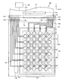
- FIG. 3 shows a plan view of the display device 100.
- FIG. FIG. 3 schematically shows the arrangement of the first detection electrode 134 and the second detection electrode 140.
- FIG. 3 shows the vertical direction as Y direction and the horizontal direction as X direction with respect to the paper surface.
- the plurality of first detection electrodes 134 extend in the Y direction
- the plurality of second detection electrodes 140 extend in the X direction.
- a group of the plurality of first detection electrodes 134 is referred to as a first detection electrode pattern 138
- a group of the plurality of second detection electrodes 140 is referred to as a second detection electrode pattern 144.
- the shapes of the first detection electrode 134 and the second detection electrode 140 are arbitrary.
- the first detection electrode 134 and the second detection electrode 140 may be rectangular (stripe) type, or may have a shape in which diamond (diamond) type electrodes are connected as shown in FIG. .
- the detection sensitivity of the touch sensor 108 can be improved by adopting a detection electrode having a shape in which such rectangular (stripe) type or diamond (diamond) type is continuously arranged.
- the first detection electrode pattern 138 and the second detection electrode pattern 144 are disposed in a region overlapping the pixel unit 104.
- the first detection electrode and the second detection electrode are arranged to overlap at least a part of the pixel 106 (a part of the light emitting element provided in the pixel).
- the touch sensor 108 can sense the presence or absence of a touch while displaying an image such as an icon on the pixel portion 104.
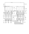
- FIG. 4 is a plan view showing the configuration of the peripheral area of the display device 100 according to an embodiment of the present invention.
- FIG. 4 is a partially enlarged view of the plan view shown in FIG. Referring to FIGS. 3 and 4, the pixel portion 104 is covered with a sealing layer 126.
- the first detection electrode 134 is electrically connected to the first wiring 136 a at the opening 133 provided in the sealing layer 126 outside the pixel portion 104.
- the first wiring 136a is electrically connected to a second terminal 115a provided in the second terminal region 112b, which is a connection terminal for a touch panel.
- the second terminal 115 a is electrically connected by the first terminal 113 a connected to the flexible printed wiring board 114 and the second wiring 137 a.
- the second detection electrode 140 is electrically connected to the first wiring 136 b provided outside the pixel unit 104.
- the first wiring 136 b is electrically connected to the second terminal 115 b of the second terminal region 112 b.
- the configurations of the first wiring 136b, the first terminal 113b, and the second terminal 115b are the same as the configurations of the first wiring 136a, the first terminal 113a, and the second terminal 115a, respectively.
- the drive circuit 110 b included in the peripheral region 118 outside the pixel portion 104 is provided with a plurality of transistors although not shown.
- the plurality of transistors include n-channel transistors, p-channel transistors, or both. Such a transistor forms a drive circuit.
- the substrate 102 is provided with an opening region 120 surrounding the pixel portion 104.
- the interlayer insulating layer on the substrate 102 includes at least one inorganic interlayer insulating layer and an organic interlayer insulating layer, and a laminated region in which the inorganic interlayer insulating layer and the organic interlayer insulating layer are laminated; And an open area where the inorganic interlayer insulating layer remains.
- the details of the opening region 120 are described by the cross-sectional structure of the pixel unit 104 described later.
- the first wires 136 a and 136 b may be drawn from the pixel portion 104 to the periphery of the substrate 102 through the top of the opening region 120.
- the opening region 120 is disposed at a position crossing the opening 133 and the second terminals 115 a and 115 b in a plan view.
- first wirings 136 a and 136 b are drawn from the pixel section 104 to the peripheral edge of the substrate 102 through the top of the opening region 120.
- the second terminal area 112 b is connected to the touch sensor control unit 109 via the flexible printed wiring board 114. That is, detection signals obtained by the first detection electrode 134 and the second detection electrode 140 are transmitted to the second terminal area 112 b by the first wires 136 a and 136 b and the second wires 137 a and 137 b, and the flexible printed wiring board 114 is It is output to the touch sensor control unit 109 via the
- the first detection electrode pattern 138 and the second detection electrode pattern 144 that constitute the sensing unit of the touch sensor 108 are provided on the substrate 102.
- the first detection electrode 134 is provided to be embedded in the sealing layer 126
- the second detection electrode 140 is provided to be in contact with the top of the sealing layer 126.
- the dielectric layer for forming a capacitance between the first detection electrode 134 and the second detection electrode 140 is replaced with a part of the sealing layer 126, so that the display device 100 can be made thin. Can be achieved.
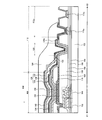
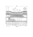
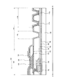
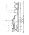
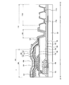
- FIG. 5 shows a cross-sectional structure of a display device 100 according to an embodiment of the present invention.
- FIG. 5 schematically shows a cross-sectional structure of the pixel portion 104 and the peripheral region 118 located outside the pixel portion 104. As shown in FIG. This cross-sectional structure corresponds to the structure along line X1-X2 shown in FIG.
- the pixel portion 104 and the peripheral region 118 are provided on the substrate 102.
- the peripheral region 118 includes a wiring portion including the first wiring 136a, and a second terminal region 112b including the first terminal 113a and the second terminal 115a.
- the peripheral region 118 includes the opening region 120 formed along the outer periphery of the region where the pixel portion 104 and the organic insulating layer 130 are formed.
- the pixel portion 104 includes a transistor 146, an organic EL element 150, a first capacitive element 152, and a second capacitive element 154. Details of the pixel 106 including these elements are shown in FIG.
- the organic EL element 150 is electrically connected to the transistor 146.
- the current flowing between the source and the drain is controlled by the video signal applied to the gate of the transistor 146, and the light emission luminance of the organic EL element 150 is controlled by this current.
- the first capacitive element 152 holds the gate voltage of the transistor 146, and the second capacitive element 154 is provided to prevent the potential of the pixel electrode 170 from being inadvertently changed.
- the second capacitive element 154 is not an essential component and can be omitted.
- a base insulating layer 156 is provided on the first surface of the substrate 102.
- the transistor 146 is provided over the base insulating layer 156.
- the transistor 146 includes a structure in which the semiconductor layer 158, the gate insulating layer 160, and the gate electrode 162 are stacked.
- the semiconductor layer 158 is formed using amorphous or polycrystalline silicon, an oxide semiconductor, or the like.
- the source / drain wiring 164 is provided in the upper layer of the gate electrode 162 via the first insulating layer 166.
- a second insulating layer 168 as a planarization layer is provided on the source / drain wiring 164.
- the first insulating layer 166 and the second insulating layer 168 are interlayer insulating layers.
- the first insulating layer 166 is a kind of inorganic interlayer insulating layer, and is formed of an inorganic insulating material such as silicon oxide, silicon nitride, silicon oxynitride, or aluminum oxide.
- the second insulating layer 168 is a type of organic interlayer insulating layer, and is formed of an organic insulating material such as polyimide or acrylic.
- the interlayer insulating layer is stacked in order of the first insulating layer 166 and the second insulating layer 168 from the substrate 102 side.
- the organic EL element 150 is provided on the top surface of the second insulating layer 168.
- the organic EL element 150 has a structure in which a pixel electrode 170 electrically connected to the transistor 146, an organic layer 172, and a counter electrode 174 are stacked.
- the organic EL element 150 is a two-terminal element, and the light emission is controlled by controlling the voltage between the pixel electrode 170 and the counter electrode 174.
- a partition layer 176 is provided on the second insulating layer 168 so as to cover the peripheral portion of the pixel electrode 170 and to expose the inner region.
- the counter electrode 174 is provided on the top surface of the organic layer 172.
- the organic layer 172 is provided from the region overlapping with the pixel electrode 170 to the upper surface portion of the partition layer 176.
- the partition layer 176 is formed of an organic resin material to cover the peripheral portion of the pixel electrode 170 and to form a smooth step at the end portion of the pixel electrode 170. Acrylic or polyimide is used
- the organic layer 172 is formed of a single layer or a plurality of layers containing an organic EL material.
- the organic layer 172 is formed using a low molecular weight or high molecular weight organic material.
- the organic layer 172 is added to the light emitting layer containing the organic EL material, and a hole injecting layer and an electron injecting layer sandwiching the light emitting layer, and a hole transporting layer and an electron transporting layer It comprises.
- the organic layer 172 can have a structure in which the light emitting layer is sandwiched between the hole injection layer and the electron injection layer.
- the organic layer 172 may be appropriately added with a hole transport layer, an electron transport layer, a hole block layer, an electron block layer, and the like.
- the organic EL element 150 has a so-called top emission type structure in which the light emitted from the organic layer 172 is emitted to the counter electrode 174 side. Therefore, the pixel electrode 170 preferably has light reflectivity.
- the pixel electrode 170 is formed of a light reflective metal material such as aluminum (Al) or silver (Ag), or ITO (Indium Tin Oxide: indium tin oxide) or IZO (indium tin oxide) excellent in hole injection property. It has a structure in which a transparent conductive layer of Indium Zinc Oxide: indium oxide / zinc oxide) and a light reflective metal layer are laminated.
- the counter electrode 174 is formed of a transparent conductive film, such as ITO or IZO, which is translucent and has conductivity in order to transmit light emitted from the organic layer 172.
- a layer containing an alkali metal such as lithium or an alkaline earth metal such as magnesium may be provided in order to enhance carrier injection.
- the first capacitor element 152 is formed in a region where the semiconductor layer 158 and the first capacitor electrode 178 overlap, using the gate insulating layer 160 as a dielectric film.
- the second capacitance element 154 uses the third insulating layer 182 provided between the pixel electrode 170 and the second capacitance electrode 180 as a dielectric film, and is provided so as to overlap with the pixel electrode 170 and the pixel electrode.
- the capacitor electrode 180 is formed.
- the third insulating layer 182 is formed of an inorganic insulating material such as silicon nitride.
- a sealing layer 126 is provided in the upper layer of the organic EL element 150.
- the sealing layer 126 is provided to prevent moisture and the like from intruding into the organic EL element 150.
- the sealing layer 126 has a structure in which the first inorganic insulating layer 128, the organic insulating layer 130, and the second inorganic insulating layer 132 are stacked from the organic EL element 150 side.
- the first inorganic insulating layer 128 and the second inorganic insulating layer 132 are formed of an inorganic insulating material such as silicon nitride, silicon oxynitride, or aluminum oxide.
- the first inorganic insulating layer 128 and the second inorganic insulating layer 132 are formed of films of these inorganic insulating materials by a sputtering method, a plasma CVD method, or the like.
- the first inorganic insulating layer 128 and the second inorganic insulating layer 132 are formed to a thickness of 0.1 ⁇ m to 10 ⁇ m, preferably 0.5 ⁇ m to 5 ⁇ m.
- the organic insulating layer 130 is preferably formed of an acrylic resin, a polyimide resin, an epoxy resin, or the like.
- the organic insulating layer 130 is provided with a thickness of 1 ⁇ m to 20 ⁇ m, preferably 2 ⁇ m to 10 ⁇ m.
- the organic insulating layer 130 is formed by a coating method such as spin coating or a vapor deposition method using an organic material source.
- the organic insulating layer 130 is formed in a predetermined region including the pixel portion 104 so as to cover the pixel portion 104 and to seal the end portion with the first inorganic insulating layer 128 and the second inorganic insulating layer 132. Is preferred. For example, as shown in FIG.
- the end (outline portion) of the organic insulating layer 130 is preferably provided between the pixel portion 104 and the opening region 120. Therefore, the organic insulating layer 130 is formed on the entire surface of the substrate 102 by a coating method, and then an outer peripheral region is removed by etching, or an evaporation method (mask evaporation) using a mask that opens a deposition surface, inkjet printing, It is preferable to form in advance a predetermined pattern by flexographic printing or gravure printing. Furthermore, as shown in FIG. 5, an overcoat layer 184 covering the wiring portion and the second terminal 115a in the pixel portion 104 and the peripheral region 118 and exposing the first terminal 113a is provided in the upper layer of the sealing layer 126. It may be provided.
- a polarizing plate 116 is provided on the upper surface of the sealing layer 126 as shown in FIG.
- the polarizing plate 116 may appropriately include a color filter layer and a light shielding layer in addition to the polarizer.
- the first detection electrode 134 of the touch sensor 108 is provided between the first inorganic insulating layer 128 and the organic insulating layer 130, and the second detection electrode 140 is provided on the second inorganic insulating layer 132.
- the first detection electrode 134 and the second detection electrode 140 may be transparent electrodes formed of a transparent conductive film in order to transmit light emitted from the organic EL element 150.
- a film of ITO or IZO, which is a kind of transparent conductive film, is produced by sputtering.
- the first detection electrode 134 and the second detection electrode 140 may be manufactured as a transparent electrode by a printing method using metal nanowires other than oxide conductive materials such as ITO and IZO, or a mesh using a metal film It may be metal wiring.
- the mesh metal wiring means a shape obtained by forming the conductive layer portion constituting the first detection electrode 134 and the second detection electrode 140 only in the region not overlapping the organic EL element 150.
- at least one of the first detection electrode 134 and the second detection electrode 140 is formed of mesh wiring having a laminated structure including a titanium (Ti) layer, an aluminum (Al) layer, and a titanium (Ti) layer. May be
- the first detection electrode 134 is formed of mesh wiring having a laminated structure including a titanium layer, an aluminum layer, and a titanium layer
- the second detection electrode 140 is a diamond electrode formed of a transparent conductive film such as ITO or IZO. It may be.
- the first detection electrode 134 forms an opening 133 for electrically connecting to the first wires 136a and 136b on the second inorganic insulating layer 132, and the first terminal region 112a and the second terminal region
- titanium is positioned on the outermost surface of the first detection electrode 134, so the process likelihood is increased.
- each of the first detection electrode 134 and the second detection electrode 140 may be formed of mesh wiring having a laminated structure including a titanium layer, an aluminum layer, and a titanium layer.
- the first detection electrode 134 forms an opening 133 for electrically connecting to the first wires 136 a and 136 b on the second inorganic insulating layer 132, and the first terminal region 112 a and the second terminal.
- titanium is positioned on the outermost surface of the first detection electrode 134, so the process likelihood is increased.
- the lead wiring is formed of a transparent conductive film such as ITO or IZO. Unlike in the case, it is not necessary to consider the reduction in film thickness due to the etching, so it is not necessary to increase the film thickness, and low resistance can be realized.
- the organic insulating layer 130 is formed on the upper layer of the first detection electrode 134, even if foreign matter adheres after the transparent conductive film or the like for forming the first detection electrode 134 is formed, The foreign matter can be coated with the organic insulating layer 130. Thus, a short circuit between the second detection electrode 140 formed on the organic insulating layer 130 and the first detection electrode 134 can be prevented. Furthermore, since the second inorganic insulating layer 132 is provided on the organic insulating layer 130, the function as the sealing layer 126 can be maintained.
- the opening region 120 is provided between the pixel portion 104 and the drive circuit 110 b.
- the opening region 120 includes an opening penetrating the second insulating layer 168.
- the opening region 120 is provided along at least one side of the pixel portion 104.
- the opening region 120 is provided to surround the pixel portion 104.
- the second insulating layer 168 is divided into the pixel portion 104 side and the drive circuit 110 b side by the opening region 120. In other words, at the opening of the opening region 120, the second insulating layer 168 formed of an organic material is removed.
- the organic insulating layer 130 constituting the sealing layer 126 has an end disposed between the opening region 120 and the pixel portion 104.
- the first inorganic insulating layer 128 and the second inorganic insulating layer 132 are extended to the outside of the end of the organic insulating layer 130.
- a structure in which the first inorganic insulating layer 128 and the second inorganic insulating layer 132 are in contact with each other is formed.
- the organic insulating layer 130 is sandwiched between the first inorganic insulating layer 128 and the second inorganic insulating layer 132, and has a structure in which the end portion is not exposed. This structure can prevent moisture and the like from infiltrating from the end portion of the organic insulating layer 130.
- the second insulating layer 168 formed of the organic insulating material in the peripheral region 118 is divided by the opening region 120, and the inorganic material layer is provided to cover the side surface and the bottom surface of the opening region 120.
- the sealing structure is formed.
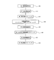
- FIG. 7 is a flowchart for explaining the method of manufacturing the display device 100 according to the embodiment of the present invention, and shows the steps of manufacturing the sealing layer 126, the first detection electrode 134, and the second detection electrode 140.
- the organic EL element 150 is formed on one main surface of the substrate 102 having the insulating surface, and then the first inorganic insulating layer 128 is manufactured (FIG. 7, S10).
- FIG. 12 shows a cross-sectional view of the display device 100 at this stage. As shown in FIG. 12, after the transistor 146, the organic EL element 150, the first capacitance element 152, the second capacitance element 154, the second terminal 115, and the opening region 120 are formed on the substrate 102, they are covered.
- the first inorganic insulating layer 128 is formed.
- the first inorganic insulating layer 128 is manufactured by a vapor deposition method such as plasma CVD (Chemical Vapor Deposition) method.
- the first inorganic insulating layer 128 is formed of a silicon nitride film, a silicon oxynitride film, or the like.
- the first detection electrode 134 is produced (FIG. 7, S12 and S14). As shown in FIG. 13, the first detection electrode 134 is formed on the first inorganic insulating layer 128. In order to produce the first detection electrode 134, first, a transparent conductive film such as IZO is formed on substantially the entire surface of the first inorganic insulating layer 134 by sputtering (FIG. 7, S12). Thereafter, the first detection electrode 134 is formed by patterning into a predetermined shape by a photolithography process (FIG. 7, S14).
- the organic insulating layer 130 is formed by a printing method or the like (FIG. 7, S16). As shown in FIG. 14, the organic insulating layer 130 is formed to cover the pixel portion 104 and not to protrude from the opening region 120.
- the organic insulating layer 130 is manufactured by an inkjet method or the like.
- the organic insulating layer 130 is formed by discharging a composition containing a precursor of a predetermined organic resin material such as an acrylic resin, a polyimide resin, or an epoxy resin from an ink head, applying the composition on the pixel portion 104 and baking it. It is made.
- the organic insulating layer 130 may be formed through a development process using a photosensitive material.
- the second inorganic insulating layer 132 is formed (FIG. 7, S18). As shown in FIG. 14, the second inorganic insulating layer 132 is formed on substantially the entire surface of the substrate 102. The second inorganic insulating layer 132 covers the organic insulating layer 130 and covers the first detection electrode 134 in a region where the organic insulating layer 130 is not provided and is in close contact with the first inorganic insulating layer 128 in a region outside the first detection electrode 134. Is formed.
- the sealing layer 126 is formed by the above steps. At this stage, since the sealing layer 126 covers the first terminal region 112a and the second terminal region 112b, in order to remove the sealing layer 126 covering these regions, the first inorganic insulating layer 128 and the second inorganic insulating layer 128 may be used.
- a step of patterning the inorganic insulating layer 132 is performed (FIG. 7, S20).
- FIG. 15 shows a stage in which a mask is formed on the first inorganic insulating layer 132 by a photolithography process to expose the second terminal region 112b. At this stage, the openings 133 for exposing the first detection electrodes 134 are simultaneously formed in the second inorganic insulating layer 132 simultaneously.
- the first detection electrode 140 is manufactured (FIG. 7, S22 and S24).
- the second detection electrode 140 is formed on the second inorganic insulating layer 134.
- a transparent conductive film such as IZO is formed on substantially the entire surface of the second inorganic insulating layer 132 by sputtering (FIG. 7, S22).
- the second detection electrode 140 is formed as shown in FIG. 5 by being patterned into a predetermined shape by a photolithography process (FIG. 7, S24).
- the first detection electrode 134 is used.
- An opening 133 to be exposed is formed in the second inorganic insulating layer 132.
- the opening 133 And the removal of the inorganic insulating layer of the second terminal region 112b can be collectively patterned in the same etching process. Thereby, the manufacturing process of the display device 100 can be reduced, and the manufacturing cost can be reduced.
- the display device since the dielectric layer for forming a capacitance between the first detection electrode 134 and the second detection electrode 140 is replaced with a part of the sealing layer 126, the display device It is possible to reduce the thickness by reducing the number of layers.
- the step of forming the contact hole to be the opening 133 on the second inorganic insulating layer 132 and the step of removing the inorganic insulating layer on the second terminal region (terminal extraction) can be simultaneously patterned, Since the reduction in the number of layers of the display device and the manufacturing process can be realized simultaneously, the manufacturing cost can be reduced.
- the number of layers of the display device is reduced, the light emission efficiency is improved, and the yield at the time of product manufacture is also improved.
- Such a structure is also applicable to a sheet-like substrate in which the substrate 102 is formed of an organic resin material, and a reduction in the number of layers and manufacturing processes can be realized in a flexible display incorporating a touch panel.
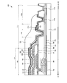
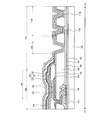
- FIG. 8 is a plan view showing the configuration of the peripheral area of the display device 200 according to the present embodiment
- FIG. 9 is a cross-sectional view showing the configuration of the display device 200 according to the present embodiment.
- the display device 200 shown in FIGS. 8 and 9 is provided with an opening 133 connecting the first detection electrode 134 and the first wiring 136 outside the opening region 120. It is done.
- the first wiring 136 is extended to the opening 133 across the opening area 120.
- the display device 200 shown in FIGS. 8 and 9 has the first detection electrode 134 of the touch sensor 108 that is composed of the organic insulating layer 130 and the second inorganic insulating layer 132. It is provided between. Therefore, in the display device 200, the sensing unit configured by the first detection electrode 134 and the second detection electrode 140 of the touch sensor 108 is insulated by the second inorganic insulating layer 132 located therebetween.
- the first detection electrode 134 and the second detection electrode 140 are insulated by at least the second inorganic insulating layer 132, the first detection electrode 134 is also the same as the display device 100 in the present embodiment, It may be provided between the first inorganic insulating layer 128 and the organic insulating layer 130.
- the other configuration of the display device 200 according to the present embodiment is the same as that of the display device 100 according to the first embodiment, and the same function and effect can be obtained.
- the first detection electrode 134 includes the first inorganic insulating layer 128 and the second inorganic insulating layer 132 constituting the sealing layer 126 up to the vicinity of the second terminal region 102b.
- the sandwiching arrangement can further reduce the deterioration and corrosion of the wiring, and can improve the reliability of the touch sensor.
- FIG. 10 is a plan view showing the configuration of the peripheral area of the display device 300 according to the present embodiment
- FIG. 11 is a cross-sectional view showing the configuration of the display device 300 according to the present embodiment.
- the opening region 120 is provided outside the second terminals 115 a and 115 b, and the first detection electrode 134.
- An opening 133 for connecting the first wiring 136 and the first wiring 136 is provided inside the second terminals 115a and 115b.
- the other configuration of the display device 300 is the same as that of the display device 100.
- the first wiring 136 is connected to the second terminals 115 a and 115 b via the opening 133 inside the opening area 120 without crossing the opening area 120.
- the wiring length of the first wiring 136 is shortened, and the first wiring 136 does not need to get over the step due to the opening region 120, so the deterioration of the wiring is prevented and the reliability of the touch sensor is improved. It can be done.
- the other configuration of the display device 300 according to the present embodiment is the same as that of the display device 100 according to the first embodiment, and the same function and effect can be obtained.
Landscapes
- Engineering & Computer Science (AREA)
- Theoretical Computer Science (AREA)
- General Engineering & Computer Science (AREA)
- Physics & Mathematics (AREA)
- General Physics & Mathematics (AREA)
- Human Computer Interaction (AREA)
- Inorganic Chemistry (AREA)
- Chemical & Material Sciences (AREA)
- Microelectronics & Electronic Packaging (AREA)
- Devices For Indicating Variable Information By Combining Individual Elements (AREA)
- Manufacturing & Machinery (AREA)
- Computer Networks & Wireless Communication (AREA)
- Optics & Photonics (AREA)
- Electroluminescent Light Sources (AREA)
Priority Applications (2)
| Application Number | Priority Date | Filing Date | Title |
|---|---|---|---|
| CN201880048513.6A CN110959147B (zh) | 2017-08-10 | 2018-08-09 | 显示装置 |
| US16/773,066 US20200159356A1 (en) | 2017-08-10 | 2020-01-27 | Display device |
Applications Claiming Priority (2)
| Application Number | Priority Date | Filing Date | Title |
|---|---|---|---|
| JP2017155333A JP6906397B2 (ja) | 2017-08-10 | 2017-08-10 | 表示装置 |
| JP2017-155333 | 2017-08-10 |
Related Child Applications (1)
| Application Number | Title | Priority Date | Filing Date |
|---|---|---|---|
| US16/773,066 Continuation US20200159356A1 (en) | 2017-08-10 | 2020-01-27 | Display device |
Publications (1)
| Publication Number | Publication Date |
|---|---|
| WO2019031579A1 true WO2019031579A1 (ja) | 2019-02-14 |
Family
ID=65272437
Family Applications (1)
| Application Number | Title | Priority Date | Filing Date |
|---|---|---|---|
| PCT/JP2018/029905 Ceased WO2019031579A1 (ja) | 2017-08-10 | 2018-08-09 | 表示装置 |
Country Status (4)
| Country | Link |
|---|---|
| US (1) | US20200159356A1 (enExample) |
| JP (2) | JP6906397B2 (enExample) |
| CN (1) | CN110959147B (enExample) |
| WO (1) | WO2019031579A1 (enExample) |
Cited By (3)
| Publication number | Priority date | Publication date | Assignee | Title |
|---|---|---|---|---|
| CN112103311A (zh) * | 2019-06-18 | 2020-12-18 | 三星显示有限公司 | 显示设备 |
| KR20230164674A (ko) | 2021-03-26 | 2023-12-04 | 린텍 가부시키가이샤 | 적층체 |
| WO2024033737A1 (ja) * | 2022-08-10 | 2024-02-15 | 株式会社半導体エネルギー研究所 | タッチパネル、及びタッチパネルの作製方法 |
Families Citing this family (6)
| Publication number | Priority date | Publication date | Assignee | Title |
|---|---|---|---|---|
| JP7110764B2 (ja) * | 2017-10-17 | 2022-08-02 | 株式会社デンソー | ヒータ装置 |
| WO2021081988A1 (zh) * | 2019-11-01 | 2021-05-06 | 京东方科技集团股份有限公司 | 显示模组和显示装置 |
| CN114442832B (zh) * | 2020-11-04 | 2024-09-17 | 宸美(厦门)光电有限公司 | 触控面板及其制造方法 |
| KR20220072017A (ko) | 2020-11-23 | 2022-06-02 | 삼성디스플레이 주식회사 | 표시 장치 및 그 제조 방법 |
| US11675448B2 (en) | 2020-12-11 | 2023-06-13 | Tpk Advanced Solutions Inc. | Touch panel and method for forming the same |
| KR20250031265A (ko) * | 2023-08-28 | 2025-03-07 | 엘지디스플레이 주식회사 | 표시 장치 및 이의 제조 방법 |
Citations (6)
| Publication number | Priority date | Publication date | Assignee | Title |
|---|---|---|---|---|
| JP2008281615A (ja) * | 2007-05-08 | 2008-11-20 | Seiko Epson Corp | 電気光学装置及びその製造方法、電子機器 |
| JP2015007945A (ja) * | 2013-06-26 | 2015-01-15 | 株式会社ジャパンディスプレイ | 端子接続構造及びタッチセンサ内蔵表示装置 |
| JP2015050245A (ja) * | 2013-08-30 | 2015-03-16 | 株式会社ジャパンディスプレイ | タッチセンサ内蔵有機エレクトロルミネッセンス装置 |
| JP2015228210A (ja) * | 2014-05-02 | 2015-12-17 | 株式会社半導体エネルギー研究所 | タッチセンサ、及びタッチパネル |
| JP2017068928A (ja) * | 2015-09-28 | 2017-04-06 | セイコーエプソン株式会社 | 有機発光装置および電子機器 |
| JP2017091135A (ja) * | 2015-11-09 | 2017-05-25 | 三菱電機株式会社 | タッチスクリーン、タッチパネル、表示装置および電子機器 |
Family Cites Families (13)
| Publication number | Priority date | Publication date | Assignee | Title |
|---|---|---|---|---|
| JP5120528B2 (ja) * | 2006-03-29 | 2013-01-16 | カシオ計算機株式会社 | 表示装置の製造方法 |
| KR100838082B1 (ko) * | 2007-03-16 | 2008-06-16 | 삼성에스디아이 주식회사 | 유기발광 표시장치 및 그 제조방법 |
| JP5267845B2 (ja) * | 2008-03-05 | 2013-08-21 | カシオ計算機株式会社 | 表示装置の製造方法 |
| KR20150011231A (ko) | 2013-07-22 | 2015-01-30 | 삼성디스플레이 주식회사 | 유기 발광 표시 장치 및 이의 제조 방법 |
| JP6371094B2 (ja) * | 2014-03-31 | 2018-08-08 | 株式会社ジャパンディスプレイ | 有機el表示装置 |
| KR102284754B1 (ko) * | 2014-10-27 | 2021-08-03 | 삼성디스플레이 주식회사 | 박막 트랜지스터 어레이 기판, 및 이를 포함하는 유기 발광 표시 장치 |
| JP2016201216A (ja) * | 2015-04-08 | 2016-12-01 | 株式会社ジャパンディスプレイ | 表示装置及び表示装置の製造方法 |
| US10168844B2 (en) | 2015-06-26 | 2019-01-01 | Samsung Display Co., Ltd. | Flexible display device |
| KR102528294B1 (ko) * | 2015-11-12 | 2023-05-04 | 삼성디스플레이 주식회사 | 유기 발광 표시 장치 및 그 제조 방법 |
| US9837475B2 (en) * | 2015-12-21 | 2017-12-05 | Japan Display Inc. | Display device |
| JP6636807B2 (ja) | 2016-01-15 | 2020-01-29 | 株式会社ジャパンディスプレイ | 有機el表示装置 |
| KR102456154B1 (ko) | 2016-01-29 | 2022-10-19 | 삼성디스플레이 주식회사 | 센서, 터치 센서 및 표시 장치 |
| KR102810070B1 (ko) | 2016-12-27 | 2025-05-21 | 엘지디스플레이 주식회사 | 표시 장치 |
-
2017
- 2017-08-10 JP JP2017155333A patent/JP6906397B2/ja active Active
-
2018
- 2018-08-09 WO PCT/JP2018/029905 patent/WO2019031579A1/ja not_active Ceased
- 2018-08-09 CN CN201880048513.6A patent/CN110959147B/zh active Active
-
2020
- 2020-01-27 US US16/773,066 patent/US20200159356A1/en not_active Abandoned
-
2021
- 2021-06-29 JP JP2021107983A patent/JP7119180B2/ja active Active
Patent Citations (6)
| Publication number | Priority date | Publication date | Assignee | Title |
|---|---|---|---|---|
| JP2008281615A (ja) * | 2007-05-08 | 2008-11-20 | Seiko Epson Corp | 電気光学装置及びその製造方法、電子機器 |
| JP2015007945A (ja) * | 2013-06-26 | 2015-01-15 | 株式会社ジャパンディスプレイ | 端子接続構造及びタッチセンサ内蔵表示装置 |
| JP2015050245A (ja) * | 2013-08-30 | 2015-03-16 | 株式会社ジャパンディスプレイ | タッチセンサ内蔵有機エレクトロルミネッセンス装置 |
| JP2015228210A (ja) * | 2014-05-02 | 2015-12-17 | 株式会社半導体エネルギー研究所 | タッチセンサ、及びタッチパネル |
| JP2017068928A (ja) * | 2015-09-28 | 2017-04-06 | セイコーエプソン株式会社 | 有機発光装置および電子機器 |
| JP2017091135A (ja) * | 2015-11-09 | 2017-05-25 | 三菱電機株式会社 | タッチスクリーン、タッチパネル、表示装置および電子機器 |
Cited By (7)
| Publication number | Priority date | Publication date | Assignee | Title |
|---|---|---|---|---|
| CN112103311A (zh) * | 2019-06-18 | 2020-12-18 | 三星显示有限公司 | 显示设备 |
| EP3754716A1 (en) * | 2019-06-18 | 2020-12-23 | Samsung Display Co., Ltd. | Display apparatus |
| US11189668B2 (en) | 2019-06-18 | 2021-11-30 | Samsung Display Co., Ltd. | Display apparatus |
| US11793051B2 (en) | 2019-06-18 | 2023-10-17 | Samsung Display Co., Ltd. | Display apparatus |
| US12329014B2 (en) | 2019-06-18 | 2025-06-10 | Samsung Display Co., Ltd. | Display apparatus |
| KR20230164674A (ko) | 2021-03-26 | 2023-12-04 | 린텍 가부시키가이샤 | 적층체 |
| WO2024033737A1 (ja) * | 2022-08-10 | 2024-02-15 | 株式会社半導体エネルギー研究所 | タッチパネル、及びタッチパネルの作製方法 |
Also Published As
| Publication number | Publication date |
|---|---|
| JP6906397B2 (ja) | 2021-07-21 |
| US20200159356A1 (en) | 2020-05-21 |
| JP7119180B2 (ja) | 2022-08-16 |
| CN110959147B (zh) | 2023-11-21 |
| CN110959147A (zh) | 2020-04-03 |
| JP2021180007A (ja) | 2021-11-18 |
| JP2019036016A (ja) | 2019-03-07 |
Similar Documents
| Publication | Publication Date | Title |
|---|---|---|
| US11778879B2 (en) | Display device including concave/convex structure in the inorganic insulation layer | |
| JP7119180B2 (ja) | 表示装置 | |
| US11054937B2 (en) | Display device having detection electrode | |
| CN107797689B (zh) | 显示装置 | |
| US10678389B2 (en) | Touch sensor and touch display device having a plurality of touch sensor layers | |
| US20180197924A1 (en) | Touch sensor and display device having touch sensor | |
| CN107689386A (zh) | 显示装置 | |
| JP6815173B2 (ja) | タッチセンサ及び表示装置 | |
| JP2017220174A (ja) | 表示装置 | |
| JP2019124776A (ja) | 表示装置および表示装置の製造方法 | |
| JP2018081917A (ja) | タッチセンサ内蔵有機el装置 |
Legal Events
| Date | Code | Title | Description |
|---|---|---|---|
| 121 | Ep: the epo has been informed by wipo that ep was designated in this application |
Ref document number: 18844050 Country of ref document: EP Kind code of ref document: A1 |
|
| NENP | Non-entry into the national phase |
Ref country code: DE |
|
| 122 | Ep: pct application non-entry in european phase |
Ref document number: 18844050 Country of ref document: EP Kind code of ref document: A1 |