WO2019013111A1 - レギュレーションプレート、アノードホルダ、及び基板ホルダ - Google Patents
レギュレーションプレート、アノードホルダ、及び基板ホルダ Download PDFInfo
- Publication number
- WO2019013111A1 WO2019013111A1 PCT/JP2018/025622 JP2018025622W WO2019013111A1 WO 2019013111 A1 WO2019013111 A1 WO 2019013111A1 JP 2018025622 W JP2018025622 W JP 2018025622W WO 2019013111 A1 WO2019013111 A1 WO 2019013111A1
- Authority
- WO
- WIPO (PCT)
- Prior art keywords
- substrate
- holder
- shielding
- anode
- square
- Prior art date
- Legal status (The legal status is an assumption and is not a legal conclusion. Google has not performed a legal analysis and makes no representation as to the accuracy of the status listed.)
- Ceased
Links
Images






Classifications
-
- C—CHEMISTRY; METALLURGY
- C25—ELECTROLYTIC OR ELECTROPHORETIC PROCESSES; APPARATUS THEREFOR
- C25D—PROCESSES FOR THE ELECTROLYTIC OR ELECTROPHORETIC PRODUCTION OF COATINGS; ELECTROFORMING; APPARATUS THEREFOR
- C25D17/00—Constructional parts, or assemblies thereof, of cells for electrolytic coating
- C25D17/10—Electrodes, e.g. composition, counter electrode
- C25D17/12—Shape or form
-
- C—CHEMISTRY; METALLURGY
- C25—ELECTROLYTIC OR ELECTROPHORETIC PROCESSES; APPARATUS THEREFOR
- C25D—PROCESSES FOR THE ELECTROLYTIC OR ELECTROPHORETIC PRODUCTION OF COATINGS; ELECTROFORMING; APPARATUS THEREFOR
- C25D17/00—Constructional parts, or assemblies thereof, of cells for electrolytic coating
-
- C—CHEMISTRY; METALLURGY
- C25—ELECTROLYTIC OR ELECTROPHORETIC PROCESSES; APPARATUS THEREFOR
- C25D—PROCESSES FOR THE ELECTROLYTIC OR ELECTROPHORETIC PRODUCTION OF COATINGS; ELECTROFORMING; APPARATUS THEREFOR
- C25D17/00—Constructional parts, or assemblies thereof, of cells for electrolytic coating
- C25D17/001—Apparatus specially adapted for electrolytic coating of wafers, e.g. semiconductors or solar cells
-
- C—CHEMISTRY; METALLURGY
- C25—ELECTROLYTIC OR ELECTROPHORETIC PROCESSES; APPARATUS THEREFOR
- C25D—PROCESSES FOR THE ELECTROLYTIC OR ELECTROPHORETIC PRODUCTION OF COATINGS; ELECTROFORMING; APPARATUS THEREFOR
- C25D17/00—Constructional parts, or assemblies thereof, of cells for electrolytic coating
- C25D17/007—Current directing devices
-
- C—CHEMISTRY; METALLURGY
- C25—ELECTROLYTIC OR ELECTROPHORETIC PROCESSES; APPARATUS THEREFOR
- C25D—PROCESSES FOR THE ELECTROLYTIC OR ELECTROPHORETIC PRODUCTION OF COATINGS; ELECTROFORMING; APPARATUS THEREFOR
- C25D17/00—Constructional parts, or assemblies thereof, of cells for electrolytic coating
- C25D17/008—Current shielding devices
-
- C—CHEMISTRY; METALLURGY
- C25—ELECTROLYTIC OR ELECTROPHORETIC PROCESSES; APPARATUS THEREFOR
- C25D—PROCESSES FOR THE ELECTROLYTIC OR ELECTROPHORETIC PRODUCTION OF COATINGS; ELECTROFORMING; APPARATUS THEREFOR
- C25D17/00—Constructional parts, or assemblies thereof, of cells for electrolytic coating
- C25D17/06—Suspending or supporting devices for articles to be coated
-
- C—CHEMISTRY; METALLURGY
- C25—ELECTROLYTIC OR ELECTROPHORETIC PROCESSES; APPARATUS THEREFOR
- C25D—PROCESSES FOR THE ELECTROLYTIC OR ELECTROPHORETIC PRODUCTION OF COATINGS; ELECTROFORMING; APPARATUS THEREFOR
- C25D17/00—Constructional parts, or assemblies thereof, of cells for electrolytic coating
- C25D17/10—Electrodes, e.g. composition, counter electrode
-
- C—CHEMISTRY; METALLURGY
- C25—ELECTROLYTIC OR ELECTROPHORETIC PROCESSES; APPARATUS THEREFOR
- C25D—PROCESSES FOR THE ELECTROLYTIC OR ELECTROPHORETIC PRODUCTION OF COATINGS; ELECTROFORMING; APPARATUS THEREFOR
- C25D5/00—Electroplating characterised by the process; Pretreatment or after-treatment of workpieces
- C25D5/02—Electroplating of selected surface areas
- C25D5/022—Electroplating of selected surface areas using masking means
-
- H—ELECTRICITY
- H10—SEMICONDUCTOR DEVICES; ELECTRIC SOLID-STATE DEVICES NOT OTHERWISE PROVIDED FOR
- H10P—GENERIC PROCESSES OR APPARATUS FOR THE MANUFACTURE OR TREATMENT OF DEVICES COVERED BY CLASS H10
- H10P14/00—Formation of materials, e.g. in the shape of layers or pillars
- H10P14/40—Formation of materials, e.g. in the shape of layers or pillars of conductive or resistive materials
- H10P14/46—Formation of materials, e.g. in the shape of layers or pillars of conductive or resistive materials using a liquid
- H10P14/47—Electrolytic deposition, i.e. electroplating; Electroless plating
Definitions
- the present invention relates to a regulation plate, an anode holder, and a substrate holder.
- wiring, bumps (protrusive electrodes) and the like are formed on the surface of a substrate such as a semiconductor wafer or a print substrate.
- An electrolytic plating method is known as a method of forming the wirings, bumps and the like.
- a round substrate such as a wafer having a diameter of 300 mm is plated.
- the demand for not only such a circular substrate but also a square substrate is increasing, and it is required to plate the square substrate.
- substrate is disclosed by patent document 1, for example.
- plating on a circular substrate is required to form a plating film having a uniform film thickness on the substrate surface.
- the wiring pattern or the like provided on the rectangular substrate may not be uniform, and the pattern density or pattern shape may differ depending on the place.
- the thickness of the plating can be intentionally controlled partially or locally in the plane of the substrate.
- the present invention has been made in view of the above problems.
- One of the purposes is to control the plating film thickness on a square substrate partially or locally.
- a regulation plate for regulating the current between the anode and the square substrate.
- the regulation plate has a body portion having an edge forming a square opening through which current flows, and a removable shielding member for shielding at least a part of the square opening.
- an anode holder configured to hold an anode.
- the anode holder is provided with a holder body for holding the anode, an anode mask attached to the holder body, having a square opening, and shielding at least a part of the square opening. And a removable shielding member.
- a substrate holder for holding a square substrate has a holder main body having an edge forming a square opening for exposing the held square substrate, and a removable shielding member for shielding at least a part of the square opening.
- FIG. 7 is a schematic plan view showing an example of a shielding plate that can be attached to a regulation plate, an anode holder, and a substrate holder.
- FIG. 7 is a schematic plan view showing an example of a shielding plate that can be attached to a regulation plate, an anode holder, and a substrate holder.
- FIG. 7 is a schematic plan view showing an example of a shielding plate that can be attached to a regulation plate, an anode holder, and a substrate holder.
- FIG. 7 is a schematic plan view showing an example of a shielding plate that can be attached to a regulation plate, an anode holder, and a substrate holder.
- FIG. 7 is a schematic plan view showing an example of a shielding plate that can be attached to a regulation plate, an anode holder, and a substrate holder.
- FIG. 7 is a schematic plan view showing an example of a shielding plate that can be attached to a regulation plate, an anode holder, and a substrate holder. It is a schematic plan view which shows the other example of a shielding member. It is a schematic plan view which shows the other example of a shielding member. It is a schematic plan view which shows the other example of a shielding member. It is a schematic plan view which shows the other example of a shielding member. It is a schematic plan view which shows the other example of a shielding member.
- substrate at the time of attaching the shielding member of FIG. 8A to a regulation plate is shown. The example of the film thickness distribution of the plating film formed in a square board
- substrate at the time of attaching the shielding member of FIG. 8C to a regulation plate is shown.
- substrate at the time of attaching the shielding member of FIG. 8D to a regulation plate is shown.
- FIG. 1 is an overall layout view of a plating apparatus according to the present embodiment.
- the plating apparatus 100 loads a square substrate onto a substrate holder or unloads a square substrate from the substrate holder, and a processing unit 102 that processes the square substrate. It is roughly divided into the cleaning unit 120.
- the processing unit 102 further includes a pre-processing and post-processing unit 102A that performs pre-processing and post-processing of the square substrate, and a plating processing unit 102B that performs plating on the square substrate.
- the loading / unloading unit 101, the processing unit 102, and the cleaning unit 120 of the plating apparatus 100 are surrounded by separate frames (casings).
- the load / unload unit 101 has two cassette tables 125 and a substrate detaching mechanism 129.
- the cassette table 125 mounts a cassette 125a containing a square substrate.
- the substrate attaching and detaching mechanism 129 is configured to attach and detach the square substrate to a substrate holder (not shown).
- a stocker 130 for accommodating the substrate holder is provided in the vicinity (for example, below) of the substrate removal mechanism 129.
- a substrate transfer device 127 which is a transfer robot for transferring a square substrate between these units, is disposed.
- the substrate transfer device 127 is configured to be capable of traveling by the traveling mechanism 128.
- the cleaning unit 120 has a cleaning device 120 a that cleans and dries the square substrate after the plating process.
- the substrate transfer device 127 is configured to transfer the plated square substrate to the cleaning device 120a, and remove the cleaned and dried square substrate from the cleaning device 120a.
- the pre-processing and post-processing unit 102A includes a pre-wet tank 132, a pre-soak tank 133, a pre-rinse tank 134, a blow tank 135, and a rinse tank 136.
- the pre-wet tank 132 the square substrate is immersed in pure water.
- the oxide film on the surface of the conductive layer such as the seed layer formed on the surface of the square substrate is etched away.
- the pre-rinse tank 134 the square substrate after the pre-soak is cleaned with a cleaning solution (such as pure water) together with the substrate holder.
- a cleaning solution such as pure water
- the rinse tank 136 the square substrate after plating is cleaned with a cleaning solution together with the substrate holder.
- the prewet tank 132, the presoak tank 133, the prerinse tank 134, the blow tank 135, and the rinse tank 136 are arranged in this order.
- the plating processing unit 102 ⁇ / b> B includes a plurality of plating tanks 139 provided with an overflow tank 138.
- Each plating tank 139 accommodates one square substrate inside, dips the square substrate in the plating solution held inside, and performs plating such as copper plating on the surface of the square substrate.
- the type of plating solution is not particularly limited, and various plating solutions may be used depending on the application.
- the plating apparatus 100 has a substrate holder transport device 137 which is located on the side of each of these devices and transports the substrate holder together with the rectangular substrate between the devices, for example, employing a linear motor system.
- the substrate holder transfer device 137 is configured to transfer the substrate holder between the substrate removal mechanism 129, the prewet tank 132, the presoak tank 133, the prerinse tank 134, the blow tank 135, the rinse tank 136, and the plating tank 139. Be done.
- FIG. 2 is a schematic longitudinal front view showing the plating tank 139 and the overflow tank 138 of the plating processing section 102B shown in FIG.
- the plating tank 139 holds the plating solution Q inside.
- the overflow tank 138 is provided on the outer periphery of the plating tank 139 so as to receive the plating solution Q overflowing from the edge of the plating tank 139.
- One end of a plating solution supply path 140 provided with a pump P is connected to the bottom of the overflow tank 138.
- the other end of the plating solution supply path 140 is connected to a plating solution supply port 143 provided at the bottom of the plating tank 139.
- the plating solution Q accumulated in the overflow tank 138 is returned to the inside of the plating tank 139 as the pump P is driven.
- a constant temperature unit 141 for adjusting the temperature of the plating solution Q and a filter 142 for removing foreign matter in the plating solution are provided in the plating solution supply path 140.
- the substrate holder 11 holding the square substrate S1 is accommodated.
- the substrate holder 11 is disposed in the plating tank 139 so that the square substrate S1 is immersed in the plating solution Q in the vertical state.
- the anode 62 held by the anode holder 60 is disposed at a position in the plating tank 139 facing the square substrate S1.
- phosphorus-containing copper can be used as the anode 62.
- An anode mask 64 for shielding a part of the anode 62 is provided on the front side of the anode holder 60 (the side facing the square substrate S1).
- the anode mask 64 has an opening through which a line of electric force between the anode 62 and the rectangular substrate S1 passes.
- the rectangular substrate S1 and the anode 62 are electrically connected through the plating power supply 144, and a current is supplied between the rectangular substrate S1 and the anode 62 to form a plating film (copper film) on the surface of the rectangular substrate S1.
- Ru is
- a paddle 145 is disposed which reciprocates in parallel with the surface of the square substrate S1 and stirs the plating solution Q. By stirring the plating solution Q with the paddle 145, sufficient copper ions can be uniformly supplied to the surface of the square substrate S1.
- a regulation plate 50 made of a dielectric is disposed to make the potential distribution over the entire surface of the rectangular substrate S1 more uniform.
- the regulation plate 50 has a flat main body 52. Further, the main body portion 52 has a cylindrical edge portion 51 forming an opening for passing an electric line of force.
- the regulation plate 50 is configured to regulate the current between the anode 62 and the square substrate S1.
- FIG. 3 is a schematic perspective view of the regulation plate 50.
- the main body 52 of the regulation plate 50 has a substantially rectangular plate shape as a whole.
- a pair of suspending portions 53 for suspending the regulation plate 50 on the upper surface of the peripheral wall of the plating tank 139 shown in FIGS. 1 and 2 are provided.
- the main body portion 52 has a square opening 52a at a substantially central portion thereof. The square opening 52 a is formed by the main body 52 and an edge 51 provided on the main body 52.
- FIG. 4 is a schematic plan view of the anode holder 60 shown in FIG.
- the anode holder 60 has a flat plate-like anode holder main body 61 and an arm portion 63 connected to the anode holder main body 61.
- the arm portion 63 has a pair of pedestals 66, and the anode holder 60 is vertically suspended and supported by installing the pedestals 66 on the upper surface of the peripheral wall of the plating tank 139 shown in FIG.
- the arm portion 63 is provided with a connector portion 65 configured to be in contact with an electrical contact provided on the plating tank 139 when the pedestal 66 is installed on the upper surface of the peripheral wall of the plating tank 139.
- the anode holder 60 is electrically connected to the plating power supply 144 shown in FIG. 2, and a voltage and current are applied to the anode 62.
- the anode holder 60 holds the anode 62, and the periphery of the anode 62 is shielded by the anode mask 64.
- the anode mask 64 has a rectangular opening (square opening). Therefore, in the plan view shown in FIG. 4, the anode 62 is held by the anode holder 60 so as to be exposed from the square opening of the anode mask 64.
- FIG. 5 is a schematic plan view of the substrate holder 11.
- the substrate holder 11 has a flat plate-like substrate holder main body 12 made of, for example, vinyl chloride, and an arm portion 13 connected to the substrate holder main body 12.
- the arm portion 13 has a pair of pedestals 14 and the substrate holder 11 is vertically suspended and supported by installing the pedestals 14 on the upper surface of the peripheral wall of each processing tank shown in FIG.
- the arm portion 13 is provided with a connector portion 15 configured to be in contact with an electrical contact provided on the plating tank 139 when the pedestal 14 is installed on the upper surface of the peripheral wall of the plating tank 139.
- the substrate holder 11 is electrically connected to the plating power supply 144 shown in FIG. 2, and voltage and current are applied to the rectangular substrate S1 held by the substrate holder 11.
- Substrate holder 11 holds square substrate S1 such that the surface to be plated of square substrate S1 shown in FIG. 5 is exposed. In other words, the substrate holder 11 has an edge 16 that forms a square opening for exposing the held square substrate S1.
- the substrate holder 11 has an electrical contact (not shown) in contact with the surface of the rectangular substrate S1. When the substrate holder 11 holds the rectangular substrate S1, the electrical contacts contact the surface of the rectangular substrate S1, for example, along the two opposing sides of the rectangular substrate S1.
- the shape of the rectangular substrate S1 is square or rectangular. In the case of a rectangular square substrate, the electrical contacts are configured to contact two opposing sides, either the long side or the short side of the rectangular square substrate.
- the wiring pattern or the like provided on the square substrate S1 may not be uniform, and the pattern density or the pattern shape may be different depending on the place.
- the thickness of the plating can be intentionally controlled partially or locally in the plane of the substrate. Therefore, in the present embodiment, a shielding member attached to at least one of the regulation plate 50, the anode holder 60, and the substrate holder 11 in order to control partially or locally the film thickness of plating formed on the square substrate S1. use.
- FIG. 6 is a schematic cross-sectional view of the regulation plate 50 to which the shielding member according to the present embodiment is attached, the anode holder 60, and the plating tank 139 in which the substrate holder 11 is accommodated.
- a shielding member 70 is removably attached to the regulation plate 50, the anode holder 60, and the substrate holder 11.
- the shielding member 70 is attached to the tip of the edge 51 of the regulation plate 50 close to the substrate holder 11 so as to shield a part of the square opening 52 a of the regulation plate 50.
- the shielding member 70 may be attached to the side of the regulation plate 50 far from the substrate holder 11.
- the shielding member 70 when the shielding member 70 is attached to the side closer to the substrate holder 11 of the regulation plate 50, the thickness of the plating film formed on the square substrate S1 can be effectively adjusted. it can.
- the shielding member 70 is attached to the anode mask 64 of the anode holder 60 to shield a part of the square opening of the anode mask 64.
- the shielding member 70 is also attached to the edge 16 of the substrate holder 11 and shields a part of the square opening of the substrate holder 11.
- the shielding member 70 is formed of, for example, a dielectric material or the like, and can adjust the electric field between the anode holder 60, the regulation plate 50, and the substrate holder 11.
- the shielding member 70 is attached to each of the regulation plate 50, the anode holder 60, and the substrate holder 11, but the present invention is not limited to this. That is, by attaching the shielding member 70 to at least one of the regulation plate 50, the anode holder 60, and the substrate holder 11, the thickness of the plating film formed on the square substrate S1 is partially or locally thickened or reduced. be able to.
- FIGS. 7A to 7F are schematic plan views showing examples of the regulation plate 50, the anode holder 60, and the shielding member 70 that can be attached to the substrate holder 11.
- FIG. The shielding member 70 may be attached to each of the square opening 52 a of the regulation plate 50, the square opening of the anode holder 60, and a part of the current passing through the square opening of the substrate holder 11.
- the edge 72 shown in FIGS. 7A to 7F is used as a general term for the edge forming the square opening 52a of the regulation plate 50, the square opening of the anode holder 60, and the square opening of the substrate holder 11.
- a partitioning member 74 which is an example of the shielding member 70 may be attached to the edge 72.
- the partitioning member 74 is a straight rod-like member, and is configured to divide the square opening into a plurality of partitions.
- two in the vertical direction and one in the lateral direction are attached so as to cross from one side of the edge 72 to the other.
- one partition member 74 in the vertical direction and one partition member 74 in a diagonal direction are attached so as to cross from one side of the edge 72 to the other.
- the dividing member 74 can be attached to the edge 72 by any fixing means such as bolts or screws.
- the rectangular opening is divided into a plurality of sections by the dividing member 74,
- the film thickness can be adjusted according to the section.
- the partitioning member 74 is not attached to the edge 72, but attached to any place such as the main body 52 of the regulation plate 50, the anode holder main body 61 of the anode holder 60, or the substrate holder main body 12 of the substrate holder 11. Can.
- the edge 72 may be attached with a partitioning member 75 which is an example of the shielding member 70.
- the dividing member 75 is a frame-like member. Therefore, the partition member 75 can be attached to the edge 72 to divide the square opening into a plurality of sections.
- the partition member 75 is attached to coincide with the corner of the edge 72.
- one partition member 75 is attached to coincide with the corner of the edge 72, and the other partition member 74 is attached to coincide with the side of the edge 72.
- the partitioning member 75 is not attached to the edge portion 72, but attached to any place such as the main body 52 of the regulation plate 50, the anode holder main body 61 of the anode holder 60, or the substrate holder body 12 of the substrate holder 11. Can.
- the edge 72 is provided with a shaft-like support member 76.
- one support member 76 is attached in the vertical direction and one in the lateral direction so as to cross the square opening.
- the support member 76 can be attached to the edge 72 by any fixing means such as bolts or screws.
- the support member 76 is formed of a thin member to such an extent that the influence on the current passing through the square opening can be ignored. Therefore, even if the support member 76 is provided to cross the square opening, the influence of the support member 76 on the film thickness distribution of the plating film formed on the square substrate S1 is substantially absent.
- the support member 76 is not attached to the edge 72, but attached to any place such as the main body 52 of the regulation plate 50, the anode holder main body 61 of the anode holder 60, or the substrate holder main body 12 of the substrate holder 11. Can.
- a frame-like partitioning member 75 is removably attached to the support member 76.
- a shielding plate 77 which is an example of the shielding member 70, is detachably attached to the support member 76.
- the partition member 75 and the shield plate 77 can be attached to the support member 76 by any fixing means such as bolts or screws.
- the partitioning member 75 and the shielding plate 77 can be disposed on the square opening via the support member 76, the partitioning member 75 and the shielding plate 77 can be edged. There is no need to attach it directly to the 72.
- the shielding plate 77 may be attached to the dividing member 75 by any fixing means.
- FIGS. 8A to 8D are schematic plan views showing another example of the shielding member 70.
- a frame-like partitioning member 75 which is an example of the shielding member 70, is attached to match the corner of the edge 72.
- one support member 76 in the vertical direction and one support member 76 in the left-right direction are provided so as to cross the opening of the dividing member 75.
- the support member 76 can be attached to the partition member 75 by any fixing means such as a bolt or a screw.
- a shielding plate 77a is attached to the intersection of the two support members 76.
- a shielding plate 77b having a larger area than the shielding plate 77a is attached to the intersection of the two support members 76.
- a shielding plate 77c having a larger area than the shielding plate 77b is attached to the intersection of the two support members 76.
- a shielding plate 77d having a larger area than the shielding plate 77c is attached to the intersection of the two support members 76.
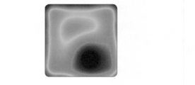
- FIGS. 9A to 9D show examples of the film thickness distribution of the plating film formed on the square substrate S1 when the shielding member 70 of FIGS. 8A to 8D is attached to the regulation plate 50, respectively.
- the film thickness of the portion corresponding to the shielding plate 77a shown in FIG. 8A is thinner than other portions.
- the film thickness distribution diagrams shown in FIGS. 9B, 9C, and 9D as the shielding area by the shielding plate 77b, the shielding plate 77c, and the shielding plate 77d becomes larger, the area of the thin film thickness part spreads .
- the film thickness of the portion of the rectangular substrate S1 corresponding to the shielded portion is the thinnest.
- the shielding member 70 including the partitioning member 74, the partitioning member 75, the shielding plate 77 and the like is at least one of the regulation plate 50, the anode holder 60, and the substrate holder 11. Can be attached to block part of the square opening.
- the plating film thickness to square substrate S1 can be controlled partially or locally.
- the film thickness is adjusted according to each section by dividing the square opening into a plurality of sections by the partitioning member 74 or the partitioning member 75 so as to correspond to the boundary of the pair of wiring patterns adjacent to each other. can do.
- the shielding member 70 can be attached at a position apart from the edge 72, so that the plating film thickness at a desired position on the rectangular substrate S1 can be adjusted. This is particularly useful when it is not desirable to affect the plating film near the periphery of the rectangular substrate S1 by the shielding member 70.
- the shielding plate 77 can be disposed in the area divided by the dividing member 74 or the dividing member 75 via the support member 76. Therefore, by dividing the square opening into a plurality of sections and arranging the shielding plate 77 in each section, it is also possible to adjust the plating film thickness on the square substrate S1 corresponding to each section.
- the shielding plate 77 is not divided through the support member 76 as shown in FIGS. 8A to 8D, but the shielding plate 77 is divided by the dividing member. It may be attached directly to 74 or the partition member 75.
- a regulation plate for regulating the current between the anode and the square substrate.
- the regulation plate has a body portion having an edge forming a square opening through which current flows, and a removable shielding member for shielding at least a part of the square opening.
- the shielding member can be attached to the regulation plate to shield a part of the square opening.
- substrate can be controlled partially or locally.
- the shielding member includes a dividing member configured to divide the square opening into a plurality of divisions.
- a group of predetermined wiring patterns is formed in a plurality on the rectangular substrate.
- the film thickness according to each section can be adjusted.
- the regulation plate of the first or second aspect has a shaft-like support member provided so as to cross the square opening, and the shielding member is detachably attached to the support member. Containing a shield.
- the shield member can be attached at a position apart from the edge of the regulation plate.
- substrate can be adjusted. This is particularly useful when it is not desirable to affect the plating film in the vicinity of the periphery of the rectangular substrate by the shielding member.
- the shielding plate is detachably attached to the support member so as not to contact the main body.
- the shield member can be attached at a position apart from the edge of the regulation plate. Thereby, the plating film thickness of the desired position on a square board
- the dividing member divides the square opening to form a plurality of openings.
- the regulation plate further includes an axial support member provided to cross at least one of the plurality of openings.
- the shielding member includes a shielding plate removably attached to the support member.
- the fifth aspect by dividing the square opening into a plurality of sections and arranging the shielding plate in each section, it is possible to adjust the plating film thickness on the square substrate corresponding to each section.
- an anode holder configured to hold an anode.
- the anode holder is provided with a holder body for holding the anode, an anode mask attached to the holder body, having a square opening, and shielding at least a part of the square opening. And a removable shielding member.
- the shielding member can be attached to the anode holder to shield a part of the square opening.
- substrate can be controlled partially or locally.
- the shielding member includes a dividing member configured to divide the square opening into a plurality of divisions.
- a group of predetermined wiring patterns is formed in a plurality on the rectangular substrate.
- the film thickness is made according to the respective sections. Can be adjusted.
- the anode holder of the sixth or seventh aspect further comprises an axial support member provided so as to cross the square opening, and the shielding member is detachably attached to the support member. Containing a shield.
- the shielding member can be attached at a position apart from the edge of the anode mask. Thereby, the plating film thickness of the desired position on a square board
- the shielding plate is detachably attached to the support member so as not to contact the holder main body and the anode mask.
- the shield member can be attached at a position apart from the edge of the anode mask.
- substrate can be adjusted. This is particularly useful when it is not desirable to affect the plating film in the vicinity of the periphery of the rectangular substrate by the shielding member.
- the dividing member divides the square opening to form a plurality of openings.
- the anode holder further includes an axial support member provided to cross at least one of the plurality of openings.
- the shielding member includes a shielding plate removably attached to the support member.
- the tenth aspect by dividing the square opening into a plurality of sections and arranging the shielding plate in each section, it is possible to adjust the plating film thickness on the square substrate corresponding to each section.
- a substrate holder for holding a square substrate has a holder main body having an edge forming a square opening for exposing the held square substrate, and a removable shielding member for shielding at least a part of the square opening.
- the shielding member can be attached to the substrate holder to shield a part of the square opening.
- substrate can be controlled partially or locally.
- the shielding member includes a partition member configured to divide the square opening into a plurality of partitions.
- a group of predetermined wiring patterns is formed in a plurality on the rectangular substrate.
- the rectangular opening is divided into a plurality of divisions by the division member so as to correspond to the boundary between the wiring pattern and the wiring pattern, so that the film thickness is made according to the respective divisions. Can be adjusted.
- a shaft-like support member provided so as to cross the square opening, and the shielding member is detachably attached to the support member. Containing a shield.
- the shielding member can be attached at a position separated from the edge of the substrate holder.
- substrate can be adjusted. This is particularly useful when it is not desirable to affect the plating film in the vicinity of the periphery of the rectangular substrate by the shielding member.
- the shielding plate is detachably attached to the support member so as not to contact the holder main body.
- the shielding member can be attached at a position apart from the edge of the substrate holder. Thereby, the plating film thickness of the desired position on a square board
- the dividing member divides the square opening to form a plurality of openings.
- the substrate holder further includes an axial support member provided to traverse at least one of the plurality of openings.
- the shielding member includes a shielding plate removably attached to the support member.
- the fifteenth aspect by dividing the square opening into a plurality of sections and arranging the shielding plate in each section, it is possible to adjust the plating film thickness on the square substrate corresponding to each section.
Landscapes
- Chemical & Material Sciences (AREA)
- Engineering & Computer Science (AREA)
- Organic Chemistry (AREA)
- Electrochemistry (AREA)
- Materials Engineering (AREA)
- Metallurgy (AREA)
- Chemical Kinetics & Catalysis (AREA)
- Life Sciences & Earth Sciences (AREA)
- Sustainable Development (AREA)
- Electroplating Methods And Accessories (AREA)
- Container, Conveyance, Adherence, Positioning, Of Wafer (AREA)
- Automation & Control Theory (AREA)
- Piezo-Electric Or Mechanical Vibrators, Or Delay Or Filter Circuits (AREA)
- Measurement Of Radiation (AREA)
Abstract
形基板へのめっき膜厚を部分的又は局所的に制御する。 アノードと角形基板との間の電流を調整するためのレギュレーションプレートが提供される。このレギュレーションプレートは、電流が通過する角形開口を形成する縁部を有する本体部と、角形開口の少なくとも一部を遮蔽するための着脱可能な遮蔽部材と、を有する。
Description
本発明は、レギュレーションプレート、アノードホルダ、及び基板ホルダに関する。
従来、半導体ウェハやプリント基板等の基板の表面に配線やバンプ(突起状電極)等を形成したりすることが行われている。この配線及びバンプ等を形成する方法として、電解めっき法が知られている。
電解めっき法に用いるめっき装置では、一般的には例えば300mmの直径を有するウェハ等の円形基板にめっき処理を行っている。しかしながら、近年の半導体市場では、費用対効果の観点から、このような円形基板に限らず、角形基板の需要が増加しており、角形基板にめっき等をすることが求められている。角形基板にめっきするめっき装置は、例えば特許文献1に開示されている。
円形基板へのめっきは、一般的に基板表面に均一な膜厚のめっき膜を形成することが求められる。一方で、角形基板では、角形基板上に設けられる配線パターン等が一様ではなく、パターン密度又はパターン形状が場所によって異なる場合があり得る。この場合、角形基板へのめっきにおいては、円形基板へのめっきと異なり、角形基板上の所定部分のみめっき膜厚を厚く又は薄くしたりする必要がある。したがって、角形基板へのめっきにおいては、基板の面内で部分的又は局所的にめっきの膜厚を意図的に制御できることが好ましい。
本発明は上記問題に鑑みてなされたものである。その目的の一つは、角形基板へのめっき膜厚を部分的又は局所的に制御することである。
本発明の一形態によれば、アノードと角形基板との間の電流を調整するためのレギュレーションプレートが提供される。このレギュレーションプレートは、電流が通過する角形開口を形成する縁部を有する本体部と、前記角形開口の少なくとも一部を遮蔽するための着脱可能な遮蔽部材と、を有する。
本発明の他の一形態によれば、アノードを保持するように構成されたアノードホルダが提供される。このアノードホルダは、前記アノードを保持するホルダ本体部と、前記ホルダ本体部に取り付けられ、角形開口を有し、前記アノードの周辺部を遮蔽するアノードマスクと、前記角形開口の少なくとも一部を遮蔽するための着脱可能な遮蔽部材と、を有する。
本発明の他の一形態によれば、角形基板を保持するための基板ホルダが提供される。この基板ホルダは、保持した前記角形基板を露出させるための角形開口を形成する縁部を有するホルダ本体部と、前記角形開口の少なくとも一部を遮蔽するための着脱可能な遮蔽部材と、を有する。
以下、本発明の実施形態について図面を参照して説明する。以下で説明する図面において、同一の又は相当する構成要素には、同一の符号を付して重複した説明を省略する。図1は、本実施形態に係るめっき装置の全体配置図である。図1に示すように、このめっき装置100は、基板ホルダに角形基板をロードし、又は基板ホルダから角形基板をアンロードするロード/アンロード部101と、角形基板を処理する処理部102と、洗浄部120とに大きく分けられる。処理部102は、さらに、角形基板の前処理及び後処理を行う前処理・後処理部102Aと、角形基板にめっき処理を行うめっき処理部102Bとを含む。めっき装置100のロード/アンロード部101と処理部102と、洗浄部120とは、それぞれ別々のフレーム(筐体)で囲まれている。
ロード/アンロード部101は、2台のカセットテーブル125と、基板脱着機構129とを有する。カセットテーブル125は、角形基板を収納したカセット125aを搭載する。基板脱着機構129は、角形基板を図示しない基板ホルダに着脱するように構成される。また、基板脱着機構129の近傍(例えば下方)には基板ホルダを収容するためのストッカ130が設けられる。これらのユニット125,129,130の中央には、これらのユニット間で角形基板を搬送する搬送用ロボットからなる基板搬送装置127が配置されている。基板搬送装置127は、走行機構128により走行可能に構成される。
洗浄部120は、めっき処理後の角形基板を洗浄して乾燥させる洗浄装置120aを有する。基板搬送装置127は、めっき処理後の角形基板を洗浄装置120aに搬送し、洗浄及び乾燥された角形基板を洗浄装置120aから取り出すように構成される。
前処理・後処理部102Aは、プリウェット槽132と、プリソーク槽133と、プリリンス槽134と、ブロー槽135と、リンス槽136と、を有する。プリウェット槽132では、角形基板が純水に浸漬される。プリソーク槽133では、角形基板の表面に形成したシード層等の導電層の表面の酸化膜がエッチング除去される。プリリンス槽134では、プリソーク後の角形基板が基板ホルダと共に洗浄液(純水等)で洗浄される。ブロー槽135では、洗浄後の角形基板の液切りが行われる。リンス槽136では、めっき後の角形基板が基板ホルダと共に洗浄液で洗浄される。プリウェット槽132、プリソーク槽133、プリリンス槽134、ブロー槽135、リンス槽136は、この順に配置されている。
めっき処理部102Bは、オーバーフロー槽138を備えた複数のめっき槽139を有する。各めっき槽139は、内部に一つの角形基板を収納し、内部に保持しためっき液中に角形基板を浸漬させて角形基板の表面に銅めっき等のめっきを行う。ここで、めっき液の種類は、特に限られることはなく、用途に応じて様々なめっき液が用いられる。
めっき装置100は、これらの各機器の側方に位置して、これらの各機器の間で基板ホルダを角形基板とともに搬送する、例えばリニアモータ方式を採用した基板ホルダ搬送装置137を有する。この基板ホルダ搬送装置137は、基板脱着機構129、プリウェット槽132、プリソーク槽133、プリリンス槽134、ブロー槽135、リンス槽136、及びめっき槽139との間で基板ホルダを搬送するように構成される。
図2は、図1に示しためっき処理部102Bのめっき槽139及びオーバーフロー槽138を示す概略縦断正面図である。図2に示すように、めっき槽139は、内部にめっき液Qを保持する。オーバーフロー槽138は、めっき槽139の縁から溢れ出ためっき液Qを受け止めるようにめっき槽139の外周に備えられている。オーバーフロー槽138の底部には、ポンプPを備えためっき液供給路140の一端が接続される。めっき液供給路140の他端は、めっき槽139の底部に設けられためっき液供給口143に接続されている。これにより、オーバーフロー槽138内に溜まっためっき液Qは、ポンプPの駆動に伴ってめっき槽139内に戻される。めっき液供給路140には、ポンプPの下流側に、めっき液Qの温度を調節する恒温ユニット141と、めっき液内の異物を除去するフィルタ142が設けられている。
めっき槽139には、角形基板S1を保持した基板ホルダ11が収納される。基板ホルダ11は、角形基板S1が鉛直状態でめっき液Qに浸漬されるように、めっき槽139内に配置される。めっき槽139内の角形基板S1に対向する位置には、アノードホルダ60に保持されたアノード62が配置される。アノード62としては、例えば、含リン銅が使用され得る。アノードホルダ60の前面側(角形基板S1と対向する側)には、アノード62の一部を遮蔽するアノードマスク64が設けられる。アノードマスク64は、アノード62と角形基板S1との間の電気力線を通過させる開口を有する。角形基板S1とアノード62は、めっき電源144を介して電気的に接続され、角形基板S1とアノード62との間に電流を流すことにより角形基板S1の表面にめっき膜(銅膜)が形成される。
角形基板S1とアノード62との間には、角形基板S1の表面と平行に往復移動してめっき液Qを攪拌するパドル145が配置される。めっき液Qをパドル145で攪拌することで、十分な銅イオンを角形基板S1の表面に均一に供給することができる。また、パドル145とアノード62との間には、角形基板S1の全面に亘る電位分布をより均一にするための誘電体からなるレギュレーションプレート50が配置される。レギュレーションプレート50は、平板状の本体部52を有する。また、この本体部52は、電気力線を通過させるための開口を形成する筒状の縁部51と、を有する。レギュレーションプレート50は、アノード62と角形基板S1との間の電流を調整するように構成される。
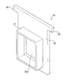
次に、図2に示したレギュレーションプレート50、アノードホルダ60、及び基板ホルダ11の形状について説明する。図3は、レギュレーションプレート50の概略斜視図である。図3に示すように、レギュレーションプレート50の本体部52は、全体として略矩形の板状である。レギュレーションプレート50の上部の左右端部には、図1及び図2に示しためっき槽139の周壁上面にレギュレーションプレート50を吊下げるための一対の吊下げ部53を有する。また、本体部52は、その略中央部に角形開口52aを有する。この角形開口52aは、本体部52及び本体部52に設けられた縁部51により形成される。
図4は、図2に示したアノードホルダ60の概略平面図である。図4に示すように、アノードホルダ60は、平板状のアノードホルダ本体61と、アノードホルダ本体61に連結されたアーム部63とを有する。アーム部63は、一対の台座66を有し、図1に示しためっき槽139の周壁上面に台座66を設置することで、アノードホルダ60が垂直に吊下げ支持される。また、アーム部63には、めっき槽139の周壁上面に台座66を設置したときに、めっき槽139に設けられた電気接点と接触するように構成されたコネクタ部65が設けられる。これにより、アノードホルダ60は図2に示しためっき電源144と電気的に接続され、アノード62に電圧・電流が印加される。
アノードホルダ60は、アノード62を保持し、このアノード62の周辺部がアノードマスク64により遮蔽される。図4に示すように、アノードマスク64は、矩形の開口(角形開口)を有する。したがって、図4に示す平面図においてアノード62はアノードマスク64の角形開口から露出されるように、アノードホルダ60に保持される。
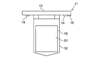
図5は、基板ホルダ11の概略平面図である。図5に示すように、基板ホルダ11は、例えば塩化ビニル製で平板状の基板ホルダ本体12と、基板ホルダ本体12に連結されたアーム部13とを有する。アーム部13は、一対の台座14を有し、図1に示した各処理槽の周壁上面に台座14を設置することで、基板ホルダ11が垂直に吊下げ支持される。また、アーム部13には、めっき槽139の周壁上面に台座14を設置したときに、めっき槽139に設けられた電気接点と接触するように構成されたコネクタ部15が設けられる。これにより、基板ホルダ11は図2に示しためっき電源144と電気的に接続され、基板ホルダ11に保持された角形基板S1に電圧・電流が印加される。
基板ホルダ11は、図5に示す角形基板S1の被めっき面が露出されるように、角形基板S1を保持する。言い換えれば、基板ホルダ11は、保持した角形基板S1を露出させるための角形開口を形成する縁部16を有する。基板ホルダ11は、角形基板S1の表面に接触する図示しない電気接点を有する。角形基板S1を基板ホルダ11が保持したとき、この電気接点は、例えば角形基板S1の対向する二辺に沿って、角形基板S1の表面と接触する。なお、角形基板S1の形状は、正方形または長方形である。長方形の角形基板の場合、電気接点は長方形の角型基板の長辺または短辺のいずれかの対向する二辺に接触するように構成される。
ところで、上述したように、角形基板S1では、角形基板S1上に設けられる配線パターン等が一様ではなく、パターン密度又はパターン形状が場所によって異なる場合があり得る。この場合、角形基板S1へのめっきにおいては、円形基板へのめっきと異なり、角形基板S1上の所定部分のみめっき膜厚を厚く又は薄くしたりする必要がある。したがって、角形基板S1へのめっきにおいては、基板の面内で部分的又は局所的にめっきの膜厚を意図的に制御できることが好ましい。そこで、本実施形態では、角形基板S1に形成するめっきの膜厚を部分的又は局所的に制御するために、レギュレーションプレート50、アノードホルダ60、及び基板ホルダ11の少なくとも一つに取り付ける遮蔽部材を使用する。
図6は、本実施形態に係る遮蔽部材を取り付けたレギュレーションプレート50、アノードホルダ60、及び基板ホルダ11を収納しためっき槽139の概略断面図である。なお、図6においては、図2に示した一部の構成が図示省略される。図6に示すように、レギュレーションプレート50、アノードホルダ60、及び基板ホルダ11には遮蔽部材70が着脱可能に取り付けられる。具体的には、遮蔽部材70は、レギュレーションプレート50の縁部51の基板ホルダ11に近い先端に取り付けられて、レギュレーションプレート50の角形開口52aの一部を遮蔽している。なお、遮蔽部材70は、レギュレーションプレート50の基板ホルダ11に遠い側に取り付けられてもよい。しかしながら、遮蔽部材70は、図6に示すように、レギュレーションプレート50の基板ホルダ11に近い側に取り付けたほうが、角形基板S1に形成されるめっき膜の厚さの調節を効果的に行うことができる。また、遮蔽部材70は、アノードホルダ60のアノードマスク64に取り付けられて、アノードマスク64の角形開口の一部を遮蔽している。同様に、遮蔽部材70は、基板ホルダ11の縁部16にも取り付けられ、基板ホルダ11の角形開口の一部を遮蔽している。
遮蔽部材70は、例えば誘電体材料等で形成され、アノードホルダ60、レギュレーションプレート50、及び基板ホルダ11の間の電場を調節することができる。なお、図6に示す例では、レギュレーションプレート50、アノードホルダ60、及び基板ホルダ11のそれぞれに遮蔽部材70が取り付けられているが、これには限られない。即ち、レギュレーションプレート50、アノードホルダ60、及び基板ホルダ11の少なくとも一つに遮蔽部材70を取り付けることで、角形基板S1に形成されるめっき膜の厚さを部分的又は局所的に厚く又は薄くすることができる。
図7Aから図7Fは、レギュレーションプレート50、アノードホルダ60、及び基板ホルダ11に取り付けることができる遮蔽部材70の例を示す概略平面図である。遮蔽部材70は、レギュレーションプレート50の角形開口52a、アノードホルダ60の角形開口、及び基板ホルダ11の角形開口を通過する電流の一部を遮蔽するように、それぞれに取り付けられ得る。図7Aから図7Fに示す縁部72は、レギュレーションプレート50の角形開口52a、アノードホルダ60の角形開口、及び基板ホルダ11の角形開口を形成する縁部の総称として用いられる。
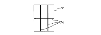
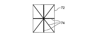
図7A及び図7Bに示す例では、遮蔽部材70の一例である区画部材74が、縁部72に取り付けられ得る。図示の例では、区画部材74は真っ直ぐな棒状の部材であり、角形開口を複数の区画に分割するように構成される。図7Aに示す例では、縁部72の一方から他方に横断するように、上下方向に2本、左右方向に1本取り付けられる。また、図7Bに示される例では、縁部72の一方から他方に横断するように、上下方向に1本、左右方向に1本、対角線上に2本の区画部材74が取り付けられる。区画部材74は、ボルト又はネジ等の任意の固定手段により、縁部72に取り付けることができる。所定の配線パターンを有する区画が角形基板S1上に複数形成されている場合には、図7A及び図7Bに示すように、区画部材74で角形開口を複数の区画に分割することにより、それぞれの区画に応じて膜厚を調整することができる。なお、区画部材74は、縁部72に取り付けるのではなく、レギュレーションプレート50の本体部52、アノードホルダ60のアノードホルダ本体61、又は基板ホルダ11の基板ホルダ本体12等、任意の場所に取り付けることができる。
図7C及び図7Dに示す例では、縁部72には、遮蔽部材70の一例である区画部材75が取り付けられ得る。図示の例では、区画部材75は枠状の部材である。したがって、区画部材75が縁部72に取り付けられることで、角形開口を複数の区画に分割することができる。図7Cに示す例では、縁部72の角に一致するように、区画部材75が取り付けられる。図7Dに示す例では、一つの区画部材75が縁部72の角に一致するように取り付けられ、他の一つの区画部材74が縁部72の辺に一致するように取り付けられる。なお、区画部材75は、縁部72に取り付けるのではなく、レギュレーションプレート50の本体部52、アノードホルダ60のアノードホルダ本体61、又は基板ホルダ11の基板ホルダ本体12等、任意の場所に取り付けることができる。
図7E及び図7Fに示す例では、縁部72には、軸状の支持部材76が設けられる。図7E及び図7Fに示すように、支持部材76は、角形開口を横断するように、上下方向に1本、及び左右方向に1本取り付けられる。支持部材76は、ボルト又はネジ等の任意の固定手段により、縁部72に取り付けることができる。支持部材76は、角形開口を通過する電流への影響を無視できる程度に細い部材で形成される。したがって、支持部材76が角形開口を横断するように設けられても、角形基板S1に形成されるめっき膜の膜厚分布に対する支持部材76による影響はほぼない。なお、支持部材76は、縁部72に取り付けるのではなく、レギュレーションプレート50の本体部52、アノードホルダ60のアノードホルダ本体61、又は基板ホルダ11の基板ホルダ本体12等、任意の場所に取り付けることができる。
図7Eに示されるように、支持部材76には、枠状の区画部材75が着脱可能に取り付けられる。また、図7Fに示されるように、支持部材76には、遮蔽部材70の一例である遮蔽板77が着脱可能に取り付けられる。区画部材75及び遮蔽板77は、ボルト又はネジ等の任意の固定手段により、支持部材76に取り付けることができる。このように、図7E及び図7Fに示した例では、支持部材76を介して区画部材75及び遮蔽板77を角形開口上に配置することができるので、区画部材75及び遮蔽板77を縁部72に直接取り付ける必要がない。これは、角形基板S1の外周近傍のめっき膜に区画部材75及び遮蔽板77による影響を与えることが望まれない場合に特に有益である。なお、遮蔽板77は、区画部材75に任意の固定手段で取り付けられてもよい。
図8Aから図8Dは、遮蔽部材70の他の例を示す概略平面図である。図8Aから図8Dに示す例では、遮蔽部材70の一例である枠状の区画部材75が縁部72の角に一致するように取り付けられる。また、この区画部材75の開口を横断するように、上下方向に1本の支持部材76と、左右方向に1本の支持部材76とが設けられる。支持部材76は、区画部材75にボルト又はネジ等の任意の固定手段により取り付けることができる。
図8Aに示す例では、2本の支持部材76の交差部分に遮蔽板77aが取り付けられる。図8Bに示す例では、2本の支持部材76の交差部分に遮蔽板77aよりも面積が大きい遮蔽板77bが取り付けられる。図8Cに示す例では、2本の支持部材76の交差部分に遮蔽板77bよりも面積が大きい遮蔽板77cが取り付けられる。図8Dに示す例では、2本の支持部材76の交差部分に遮蔽板77cよりも面積が大きい遮蔽板77dが取り付けられる。
図9Aから図9Dは、それぞれ、図8Aから図8Dの遮蔽部材70をレギュレーションプレート50に取り付けた場合の、角形基板S1に形成されるめっき膜の膜厚分布の例を示す。図9Aに示す膜厚分布図によれば、図8Aに示す遮蔽板77aに対応する部分の膜厚が他の箇所に比べて薄くなっている。図9B、図9C、及び図9Dに示す膜厚分布図によれば、遮蔽板77b、遮蔽板77c、及び遮蔽板77dによる遮蔽面積が大きくなるにつれて、膜厚が薄い部分の領域が広がっている。これに伴い、最も遮蔽面積が大きい遮蔽板77dにより角形開口が遮蔽された場合、図9Dによれば、遮蔽された部分に対応する角形基板S1の部分の膜厚が最も薄くなっている。
以上で説明したように、本実施形態によれば、区画部材74、区画部材75、及び遮蔽板77等を含む遮蔽部材70を、レギュレーションプレート50、アノードホルダ60、及び基板ホルダ11の少なくとも一つに取り付けて角形開口の一部を遮蔽することができる。これにより、角形基板S1へのめっき膜厚を部分的又は局所的に制御することができる。ひいては、円形基板の場合は通常求められない、膜厚を敢えて不均一にすることを実現することができる。
特に、角形基板S1には、ひとまとまりの所定の配線パターンが複数形成されている場合がある。このような場合は、隣接する一対の配線パターンの境界に対応するように、区画部材74又は区画部材75で角形開口を複数の区画に分割することで、それぞれの区画に応じて膜厚を調整することができる。
さらに、支持部材76を使用することで、縁部72から離間した位置に遮蔽部材70を取り付けることができるから、角形基板S1上の所望の位置のめっき膜厚を調節することができる。これは、角形基板S1の周辺近傍のめっき膜に遮蔽部材70による影響を与えることが望まれない場合に特に有益である。
また、図8A-図8Dに示したように、区画部材74又は区画部材75によって区画された領域内に、支持部材76を介して遮蔽板77を配置することもできる。したがって、角形開口を複数の区画に分割するとともに、各区画内に遮蔽板77を配置することで、各区画に対応する角形基板S1上のめっき膜厚を調節することもできる。なお、区画部材74又は区画部材75によって角形開口を区画した場合において、図8A-図8Dに示したように支持部材76を介して遮蔽板77を配置するのではなく、遮蔽板77を区画部材74又は区画部材75に直接取り付けてもよい。
以上、本発明の実施形態について説明したが、上述した発明の実施の形態は、本発明の理解を容易にするためのものであり、本発明を限定するものではない。本発明は、その趣旨を逸脱することなく、変更、改良され得るとともに、本発明にはその等価物が含まれることはもちろんである。また、上述した課題の少なくとも一部を解決できる範囲、または、効果の少なくとも一部を奏する範囲において、特許請求の範囲及び明細書に記載された各構成要素の任意の組み合わせ、又は省略が可能である。
以下に本明細書が開示する形態のいくつかを記載しておく。
第1形態によれば、アノードと角形基板との間の電流を調整するためのレギュレーションプレートが提供される。このレギュレーションプレートは、電流が通過する角形開口を形成する縁部を有する本体部と、前記角形開口の少なくとも一部を遮蔽するための着脱可能な遮蔽部材と、を有する。
第1形態によれば、遮蔽部材をレギュレーションプレートに取り付けて、角形開口の一部を遮蔽することができる。これにより、角形基板へのめっき膜厚を部分的又は局所的に制御することができる。ひいては、円形基板の場合は通常求められない、膜厚を敢えて不均一にすることを実現することができる。
第2形態によれば、第1形態のレギュレーションプレートにおいて、前記遮蔽部材は、前記角形開口を複数の区画に分割するように構成される区画部材を含む。
角形基板には、ひとまとまりの所定の配線パターンが複数形成されている場合がある。第2形態によれば、このような場合に、配線パターンと配線パターンとの境界に対応するように、区画部材で角形開口を複数の区画に分割することで、それぞれの区画に応じて膜厚を調整することができる。
第3形態によれば、第1又は第2形態のレギュレーションプレートにおいて、前記角形開口を横断するように設けられる軸状の支持部材を有し、前記遮蔽部材は、前記支持部材に着脱可能に取り付けられる遮蔽板を含む。
第3形態によれば、支持部材を使用することで、レギュレーションプレートの縁部から離間した位置に遮蔽部材を取り付けることができる。これにより、角形基板上の所望の位置のめっき膜厚を調節することができる。これは、角形基板の周辺近傍のめっき膜に遮蔽部材による影響を与えることが望まれない場合に特に有益である。
第4形態によれば、第3形態のレギュレーションプレートにおいて、前記遮蔽板は、前記本体部に接触しないように前記支持部材に着脱可能に取り付けられる。
第4形態によれば、支持部材を使用することで、レギュレーションプレートの縁部から離間した位置に遮蔽部材を取り付けることができる。これにより、角形基板上の所望の位置のめっき膜厚を調節することができる。これは、角形基板の周辺近傍のめっき膜に遮蔽部材による影響を与えることが望まれない場合に特に有益である。
第5形態によれば、第2形態のレギュレーションプレートにおいて、前記区画部材は、前記角形開口を区画して複数の開口を形成する。前記レギュレーションプレートは、さらに、前記複数の開口の少なくとも一つを横断するように設けられる軸状の支持部材を有する。前記遮蔽部材は、前記支持部材に着脱可能に取り付けられる遮蔽板を含む。
第5形態によれば、角形開口を複数の区画に分割するとともに、各区画内に遮蔽板を配置することで、各区画に対応する角形基板上のめっき膜厚を調節することができる。
第6形態によれば、アノードを保持するように構成されたアノードホルダが提供される。このアノードホルダは、前記アノードを保持するホルダ本体部と、前記ホルダ本体部に取り付けられ、角形開口を有し、前記アノードの周辺部を遮蔽するアノードマスクと、前記角形開口の少なくとも一部を遮蔽するための着脱可能な遮蔽部材と、を有する。
第6形態によれば、遮蔽部材をアノードホルダに取り付けて、角形開口の一部を遮蔽することができる。これにより、角形基板へのめっき膜厚を部分的又は局所的に制御することができる。ひいては、円形基板の場合は通常求められない、膜厚を敢えて不均一にすることを実現することができる。
第7形態によれば、第6形態のアノードホルダにおいて、前記遮蔽部材は、前記角形開口を複数の区画に分割するように構成される区画部材を含む。
角形基板には、ひとまとまりの所定の配線パターンが複数形成されている場合がある。第7形態によれば、このような場合に、配線パターンと配線パターンとの境界に対応するように、区画部材で角形開口を複数の区画に分割することで、それぞれの区画に応じて膜厚を調整することができる。
第8形態によれば、第6又は第7形態のアノードホルダにおいて、前記角形開口を横断するように設けられる軸状の支持部材を有し、前記遮蔽部材は、前記支持部材に着脱可能に取り付けられる遮蔽板を含む。
第8形態によれば、支持部材を使用することで、アノードマスクの縁部から離間した位置に遮蔽部材を取り付けることができる。これにより、角形基板上の所望の位置のめっき膜厚を調節することができる。これは、角形基板の周辺近傍のめっき膜に遮蔽部材による影響を与えることが望まれない場合に特に有益である。
第9形態によれば、第8形態のアノードホルダにおいて、前記遮蔽板は、前記ホルダ本体部及び前記アノードマスクに接触しないように前記支持部材に着脱可能に取り付けられる。
第9形態によれば、支持部材を使用することで、アノードマスクの縁部から離間した位置に遮蔽部材を取り付けることができる。これにより、角形基板上の所望の位置のめっき膜厚を調節することができる。これは、角形基板の周辺近傍のめっき膜に遮蔽部材による影響を与えることが望まれない場合に特に有益である。
第10形態によれば、第7形態のアノードホルダにおいて、前記区画部材は、前記角形開口を区画して複数の開口を形成する。前記アノードホルダは、さらに、前記複数の開口の少なくとも一つを横断するように設けられる軸状の支持部材を有する。前記遮蔽部材は、前記支持部材に着脱可能に取り付けられる遮蔽板を含む。
第10形態によれば、角形開口を複数の区画に分割するとともに、各区画内に遮蔽板を配置することで、各区画に対応する角形基板上のめっき膜厚を調節することができる。
第11形態によれば、角形基板を保持するための基板ホルダが提供される。この基板ホルダは、保持した前記角形基板を露出させるための角形開口を形成する縁部を有するホルダ本体部と、前記角形開口の少なくとも一部を遮蔽するための着脱可能な遮蔽部材と、を有する。
第11形態によれば、遮蔽部材を基板ホルダに取り付けて、角形開口の一部を遮蔽することができる。これにより、角形基板へのめっき膜厚を部分的又は局所的に制御することができる。ひいては、円形基板の場合は通常求められない、膜厚を敢えて不均一にすることを実現することができる。
第12形態によれば、第11形態の基板ホルダにおいて、前記遮蔽部材は、前記角形開口を複数の区画に分割するように構成される区画部材を含む。
角形基板には、ひとまとまりの所定の配線パターンが複数形成されている場合がある。第12形態によれば、このような場合に、配線パターンと配線パターンとの境界に対応するように、区画部材で角形開口を複数の区画に分割することで、それぞれの区画に応じて膜厚を調整することができる。
第13形態によれば、第11又は第12形態の基板ホルダにおいて、前記角形開口を横断するように設けられる軸状の支持部材を有し、前記遮蔽部材は、前記支持部材に着脱可能に取り付けられる遮蔽板を含む。
第13形態によれば、支持部材を使用することで、基板ホルダの縁部から離間した位置に遮蔽部材を取り付けることができる。これにより、角形基板上の所望の位置のめっき膜厚を調節することができる。これは、角形基板の周辺近傍のめっき膜に遮蔽部材による影響を与えることが望まれない場合に特に有益である。
第14形態によれば、第13形態の基板ホルダにおいて、前記遮蔽板は、前記ホルダ本体部に接触しないように前記支持部材に着脱可能に取り付けられる。
第14形態によれば、支持部材を使用することで、基板ホルダの縁部から離間した位置に遮蔽部材を取り付けることができる。これにより、角形基板上の所望の位置のめっき膜厚を調節することができる。これは、角形基板の周辺近傍のめっき膜に遮蔽部材による影響を与えることが望まれない場合に特に有益である。
第15形態によれば、第12形態の基板ホルダにおいて、前記区画部材は、前記角形開口を区画して複数の開口を形成する。前記基板ホルダは、さらに、前記複数の開口の少なくとも一つを横断するように設けられる軸状の支持部材を有する。前記遮蔽部材は、前記支持部材に着脱可能に取り付けられる遮蔽板を含む。
第15形態によれば、角形開口を複数の区画に分割するとともに、各区画内に遮蔽板を配置することで、各区画に対応する角形基板上のめっき膜厚を調節することができる。
S1…角形基板
11…基板ホルダ
12…基板ホルダ本体
16…縁部
50…レギュレーションプレート
51…縁部
52…本体部
52a…角形開口
60…アノードホルダ
61…アノードホルダ本体
62…アノード
64…アノードマスク
70…遮蔽部材
72…縁部
74…区画部材
75…区画部材
76…支持部材
77,77a,77b,77c,77d…遮蔽板
11…基板ホルダ
12…基板ホルダ本体
16…縁部
50…レギュレーションプレート
51…縁部
52…本体部
52a…角形開口
60…アノードホルダ
61…アノードホルダ本体
62…アノード
64…アノードマスク
70…遮蔽部材
72…縁部
74…区画部材
75…区画部材
76…支持部材
77,77a,77b,77c,77d…遮蔽板
Claims (15)
- アノードと角形基板との間の電流を調整するためのレギュレーションプレートであって、
電流が通過する角形開口を形成する縁部を有する本体部と、
前記角形開口の少なくとも一部を遮蔽するための着脱可能な遮蔽部材と、を有する、レギュレーションプレート。 - 請求項1に記載されたレギュレーションプレートにおいて、
前記遮蔽部材は、前記角形開口を複数の区画に分割するように構成される区画部材を含む、レギュレーションプレート。 - 請求項1又は2に記載されたレギュレーションプレートにおいて、
前記角形開口を横断するように設けられる軸状の支持部材を有し、
前記遮蔽部材は、前記支持部材に着脱可能に取り付けられる遮蔽板を含む、レギュレーションプレート。 - 請求項3に記載されたレギュレーションプレートにおいて、
前記遮蔽板は、前記本体部に接触しないように前記支持部材に着脱可能に取り付けられる、レギュレーションプレート。 - 請求項2に記載されたレギュレーションプレートにおいて、
前記区画部材は、前記角形開口を区画して複数の開口を形成し、
前記レギュレーションプレートは、さらに、前記複数の開口の少なくとも一つを横断するように設けられる軸状の支持部材を有し、
前記遮蔽部材は、前記支持部材に着脱可能に取り付けられる遮蔽板を含む、レギュレーションプレート。 - アノードを保持するように構成されたアノードホルダであって、
前記アノードを保持するホルダ本体部と、
前記ホルダ本体部に取り付けられ、角形開口を有し、前記アノードの周辺部を遮蔽するアノードマスクと、
前記角形開口の少なくとも一部を遮蔽するための着脱可能な遮蔽部材と、を有する、アノードホルダ。 - 請求項6に記載されたアノードホルダにおいて、
前記遮蔽部材は、前記角形開口を複数の区画に分割するように構成される区画部材を含む、アノードホルダ。 - 請求項6又は7に記載されたアノードホルダにおいて、
前記角形開口を横断するように設けられる軸状の支持部材を有し、
前記遮蔽部材は、前記支持部材に着脱可能に取り付けられる遮蔽板を含む、アノードホルダ。 - 請求項8に記載されたアノードホルダにおいて、
前記遮蔽板は、前記ホルダ本体部及び前記アノードマスクに接触しないように前記支持部材に着脱可能に取り付けられる、アノードホルダ。 - 請求項7に記載されたアノードホルダにおいて、
前記区画部材は、前記角形開口を区画して複数の開口を形成し、
前記アノードホルダは、さらに、前記複数の開口の少なくとも一つを横断するように設けられる軸状の支持部材を有し、
前記遮蔽部材は、前記支持部材に着脱可能に取り付けられる遮蔽板を含む、アノードホルダ。 - 角形基板を保持するための基板ホルダであって、
保持した前記角形基板を露出させるための角形開口を形成する縁部を有するホルダ本体部と、
前記角形開口の少なくとも一部を遮蔽するための着脱可能な遮蔽部材と、を有する、基板ホルダ。 - 請求項11に記載された基板ホルダにおいて、
前記遮蔽部材は、前記角形開口を複数の区画に分割するように構成される区画部材を含む、基板ホルダ。 - 請求項11又は12に記載された基板ホルダにおいて、
前記角形開口を横断するように設けられる軸状の支持部材を有し、
前記遮蔽部材は、前記支持部材に着脱可能に取り付けられる遮蔽板を含む、基板ホルダ。 - 請求項13に記載された基板ホルダにおいて、
前記遮蔽板は、前記ホルダ本体部に接触しないように前記支持部材に着脱可能に取り付けられる、基板ホルダ。 - 請求項12に記載された基板ホルダにおいて、
前記区画部材は、前記角形開口を区画して複数の開口を形成し、
前記基板ホルダは、さらに、前記複数の開口の少なくとも一つを横断するように設けられる軸状の支持部材を有し、
前記遮蔽部材は、前記支持部材に着脱可能に取り付けられる遮蔽板を含む、基板ホルダ。
Priority Applications (4)
| Application Number | Priority Date | Filing Date | Title |
|---|---|---|---|
| US16/630,369 US11268207B2 (en) | 2017-07-11 | 2018-07-06 | Regulation plate, anode holder, and substrate holder |
| KR1020197037760A KR102551335B1 (ko) | 2017-07-11 | 2018-07-06 | 레귤레이션 플레이트, 애노드 홀더, 및 기판 홀더 |
| CN201880045920.1A CN110914482B (zh) | 2017-07-11 | 2018-07-06 | 调节板、阳极保持器以及基板保持器 |
| US17/590,140 US11686009B2 (en) | 2017-07-11 | 2022-02-01 | Regulation plate, anode holder, and substrate holder |
Applications Claiming Priority (2)
| Application Number | Priority Date | Filing Date | Title |
|---|---|---|---|
| JP2017-135370 | 2017-07-11 | ||
| JP2017135370A JP6891060B2 (ja) | 2017-07-11 | 2017-07-11 | レギュレーションプレート、アノードホルダ、及び基板ホルダ |
Related Child Applications (2)
| Application Number | Title | Priority Date | Filing Date |
|---|---|---|---|
| US16/630,369 A-371-Of-International US11268207B2 (en) | 2017-07-11 | 2018-07-06 | Regulation plate, anode holder, and substrate holder |
| US17/590,140 Division US11686009B2 (en) | 2017-07-11 | 2022-02-01 | Regulation plate, anode holder, and substrate holder |
Publications (1)
| Publication Number | Publication Date |
|---|---|
| WO2019013111A1 true WO2019013111A1 (ja) | 2019-01-17 |
Family
ID=65001291
Family Applications (1)
| Application Number | Title | Priority Date | Filing Date |
|---|---|---|---|
| PCT/JP2018/025622 Ceased WO2019013111A1 (ja) | 2017-07-11 | 2018-07-06 | レギュレーションプレート、アノードホルダ、及び基板ホルダ |
Country Status (6)
| Country | Link |
|---|---|
| US (2) | US11268207B2 (ja) |
| JP (1) | JP6891060B2 (ja) |
| KR (1) | KR102551335B1 (ja) |
| CN (1) | CN110914482B (ja) |
| TW (1) | TWI773784B (ja) |
| WO (1) | WO2019013111A1 (ja) |
Cited By (1)
| Publication number | Priority date | Publication date | Assignee | Title |
|---|---|---|---|---|
| JP7558455B1 (ja) * | 2023-12-21 | 2024-09-30 | 株式会社荏原製作所 | めっき装置 |
Families Citing this family (8)
| Publication number | Priority date | Publication date | Assignee | Title |
|---|---|---|---|---|
| JP7256708B2 (ja) | 2019-07-09 | 2023-04-12 | 株式会社荏原製作所 | めっき装置 |
| JP7227875B2 (ja) * | 2019-08-22 | 2023-02-22 | 株式会社荏原製作所 | 基板ホルダおよびめっき装置 |
| JP7296832B2 (ja) * | 2019-09-10 | 2023-06-23 | 株式会社荏原製作所 | めっき装置 |
| CN111394758B (zh) * | 2020-05-14 | 2023-11-03 | 绍兴上虞顺风金属表面处理有限公司 | 一种基于金属表面化处理领域的电镀工艺及设备 |
| JP7069442B1 (ja) * | 2021-12-06 | 2022-05-17 | 株式会社荏原製作所 | めっき方法及びめっき装置 |
| TWI806455B (zh) * | 2022-03-01 | 2023-06-21 | 日商荏原製作所股份有限公司 | 鍍覆裝置及鍍覆方法 |
| US11913132B2 (en) * | 2022-05-18 | 2024-02-27 | Advanced Semiconductor Engineering, Inc. | Method for manufacturing a package |
| CN121760043A (zh) * | 2024-09-30 | 2026-03-31 | 盛美半导体设备(上海)股份有限公司 | 电场控制元件及电镀装置 |
Citations (5)
| Publication number | Priority date | Publication date | Assignee | Title |
|---|---|---|---|---|
| JPH0617297A (ja) * | 1992-07-02 | 1994-01-25 | Ibiden Co Ltd | 電気メッキ装置 |
| JP2005029863A (ja) * | 2003-07-10 | 2005-02-03 | Ebara Corp | めっき装置 |
| JP2008088522A (ja) * | 2006-10-04 | 2008-04-17 | Matsushita Electric Ind Co Ltd | パターンめっき方法 |
| JP2013112842A (ja) * | 2011-11-28 | 2013-06-10 | Yamaichi Electronics Co Ltd | 電気めっき装置およびめっき方法 |
| JP2016127069A (ja) * | 2014-12-26 | 2016-07-11 | 株式会社荏原製作所 | 基板ホルダ、基板ホルダで基板を保持する方法、及びめっき装置 |
Family Cites Families (12)
| Publication number | Priority date | Publication date | Assignee | Title |
|---|---|---|---|---|
| JPS6017297A (ja) * | 1983-07-07 | 1985-01-29 | Babcock Hitachi Kk | フレツテイング防止法 |
| JP2002302799A (ja) * | 2001-04-05 | 2002-10-18 | Sumitomo Metal Mining Co Ltd | 電気めっき方法および電気めっき方法で用いる遮へい板 |
| JP4942580B2 (ja) * | 2007-08-20 | 2012-05-30 | 株式会社荏原製作所 | アノードホルダ用通電ベルトおよびアノードホルダ |
| US8177944B2 (en) * | 2007-12-04 | 2012-05-15 | Ebara Corporation | Plating apparatus and plating method |
| CN201180162Y (zh) * | 2008-01-18 | 2009-01-14 | 佳辉设备(东莞)有限公司 | 活动式阴极遮蔽装置 |
| CN202323066U (zh) * | 2011-11-23 | 2012-07-11 | 天津普林电路股份有限公司 | 高密度互连电路板电镀工艺用边缘镀铜可调的遮蔽板 |
| US20140231245A1 (en) * | 2013-02-18 | 2014-08-21 | Globalfoundries Inc. | Adjustable current shield for electroplating processes |
| JP6317299B2 (ja) | 2015-08-28 | 2018-04-25 | 株式会社荏原製作所 | めっき装置、めっき方法、及び基板ホルダ |
| CN204859775U (zh) * | 2015-08-28 | 2015-12-09 | 上海美维科技有限公司 | 一种图形电镀治具 |
| CN108149293A (zh) * | 2016-12-05 | 2018-06-12 | 苏州能讯高能半导体有限公司 | 半导体晶圆电沉积方法及半导体晶圆电沉积装置 |
| KR20180126312A (ko) * | 2017-05-17 | 2018-11-27 | 삼성전기주식회사 | 도금장치 |
| CN112323112A (zh) * | 2020-11-30 | 2021-02-05 | 苏州市康普来表面处理科技有限公司 | 运用于新能源汽车零部件局部镀阴极遮蔽治具及电镀设备 |
-
2017
- 2017-07-11 JP JP2017135370A patent/JP6891060B2/ja active Active
-
2018
- 2018-07-02 TW TW107122761A patent/TWI773784B/zh active
- 2018-07-06 WO PCT/JP2018/025622 patent/WO2019013111A1/ja not_active Ceased
- 2018-07-06 CN CN201880045920.1A patent/CN110914482B/zh active Active
- 2018-07-06 US US16/630,369 patent/US11268207B2/en active Active
- 2018-07-06 KR KR1020197037760A patent/KR102551335B1/ko active Active
-
2022
- 2022-02-01 US US17/590,140 patent/US11686009B2/en active Active
Patent Citations (5)
| Publication number | Priority date | Publication date | Assignee | Title |
|---|---|---|---|---|
| JPH0617297A (ja) * | 1992-07-02 | 1994-01-25 | Ibiden Co Ltd | 電気メッキ装置 |
| JP2005029863A (ja) * | 2003-07-10 | 2005-02-03 | Ebara Corp | めっき装置 |
| JP2008088522A (ja) * | 2006-10-04 | 2008-04-17 | Matsushita Electric Ind Co Ltd | パターンめっき方法 |
| JP2013112842A (ja) * | 2011-11-28 | 2013-06-10 | Yamaichi Electronics Co Ltd | 電気めっき装置およびめっき方法 |
| JP2016127069A (ja) * | 2014-12-26 | 2016-07-11 | 株式会社荏原製作所 | 基板ホルダ、基板ホルダで基板を保持する方法、及びめっき装置 |
Cited By (2)
| Publication number | Priority date | Publication date | Assignee | Title |
|---|---|---|---|---|
| JP7558455B1 (ja) * | 2023-12-21 | 2024-09-30 | 株式会社荏原製作所 | めっき装置 |
| WO2025134313A1 (ja) * | 2023-12-21 | 2025-06-26 | 株式会社荏原製作所 | めっき装置 |
Also Published As
| Publication number | Publication date |
|---|---|
| JP6891060B2 (ja) | 2021-06-18 |
| US20220154363A1 (en) | 2022-05-19 |
| KR20200026821A (ko) | 2020-03-11 |
| JP2019014955A (ja) | 2019-01-31 |
| CN110914482A (zh) | 2020-03-24 |
| TWI773784B (zh) | 2022-08-11 |
| KR102551335B1 (ko) | 2023-07-05 |
| TW201909278A (zh) | 2019-03-01 |
| US11686009B2 (en) | 2023-06-27 |
| CN110914482B (zh) | 2022-02-22 |
| US11268207B2 (en) | 2022-03-08 |
| US20200157702A1 (en) | 2020-05-21 |
Similar Documents
| Publication | Publication Date | Title |
|---|---|---|
| WO2019013111A1 (ja) | レギュレーションプレート、アノードホルダ、及び基板ホルダ | |
| JP7220758B2 (ja) | 基板ホルダ及びめっき装置 | |
| KR102786549B1 (ko) | 기판 홀더 및 도금 장치 | |
| US10968530B2 (en) | Electroplating device | |
| CN112553661B (zh) | 镀敷装置 | |
| JP6859150B2 (ja) | めっき装置及びめっき槽構成の決定方法 | |
| CN116391063A (zh) | 镀覆装置 | |
| KR20230122175A (ko) | 도금 장치 및 도금 방법 | |
| JP7285389B1 (ja) | めっき装置、および、めっき方法 | |
| KR102744025B1 (ko) | 도금 장치 |
Legal Events
| Date | Code | Title | Description |
|---|---|---|---|
| 121 | Ep: the epo has been informed by wipo that ep was designated in this application |
Ref document number: 18831278 Country of ref document: EP Kind code of ref document: A1 |
|
| ENP | Entry into the national phase |
Ref document number: 20197037760 Country of ref document: KR Kind code of ref document: A |
|
| NENP | Non-entry into the national phase |
Ref country code: DE |
|
| 122 | Ep: pct application non-entry in european phase |
Ref document number: 18831278 Country of ref document: EP Kind code of ref document: A1 |