WO2019012372A1 - 給電装置および非接触給電システム - Google Patents
給電装置および非接触給電システム Download PDFInfo
- Publication number
- WO2019012372A1 WO2019012372A1 PCT/IB2018/054931 IB2018054931W WO2019012372A1 WO 2019012372 A1 WO2019012372 A1 WO 2019012372A1 IB 2018054931 W IB2018054931 W IB 2018054931W WO 2019012372 A1 WO2019012372 A1 WO 2019012372A1
- Authority
- WO
- WIPO (PCT)
- Prior art keywords
- potential
- coil
- current
- function
- transistor
- Prior art date
- Legal status (The legal status is an assumption and is not a legal conclusion. Google has not performed a legal analysis and makes no representation as to the accuracy of the status listed.)
- Ceased
Links
Images







Classifications
-
- H—ELECTRICITY
- H04—ELECTRIC COMMUNICATION TECHNIQUE
- H04B—TRANSMISSION
- H04B5/00—Near-field transmission systems, e.g. inductive or capacitive transmission systems
- H04B5/20—Near-field transmission systems, e.g. inductive or capacitive transmission systems characterised by the transmission technique; characterised by the transmission medium
- H04B5/24—Inductive coupling
- H04B5/26—Inductive coupling using coils
-
- H—ELECTRICITY
- H02—GENERATION; CONVERSION OR DISTRIBUTION OF ELECTRIC POWER
- H02J—ELECTRIC POWER NETWORKS; CIRCUIT ARRANGEMENTS OR SYSTEMS FOR SUPPLYING OR DISTRIBUTING ELECTRIC POWER; SYSTEMS FOR STORING ELECTRIC ENERGY
- H02J50/00—Circuit arrangements or systems for wireless supply or distribution of electric power
- H02J50/10—Circuit arrangements or systems for wireless supply or distribution of electric power using inductive coupling
- H02J50/12—Circuit arrangements or systems for wireless supply or distribution of electric power using inductive coupling of the resonant type
-
- H—ELECTRICITY
- H02—GENERATION; CONVERSION OR DISTRIBUTION OF ELECTRIC POWER
- H02J—ELECTRIC POWER NETWORKS; CIRCUIT ARRANGEMENTS OR SYSTEMS FOR SUPPLYING OR DISTRIBUTING ELECTRIC POWER; SYSTEMS FOR STORING ELECTRIC ENERGY
- H02J50/00—Circuit arrangements or systems for wireless supply or distribution of electric power
- H02J50/005—Mechanical details of housing or structure aiming to accommodate the power transfer means, e.g. mechanical integration of coils, antennas or transducers into emitting or receiving devices
-
- H—ELECTRICITY
- H02—GENERATION; CONVERSION OR DISTRIBUTION OF ELECTRIC POWER
- H02J—ELECTRIC POWER NETWORKS; CIRCUIT ARRANGEMENTS OR SYSTEMS FOR SUPPLYING OR DISTRIBUTING ELECTRIC POWER; SYSTEMS FOR STORING ELECTRIC ENERGY
- H02J50/00—Circuit arrangements or systems for wireless supply or distribution of electric power
- H02J50/10—Circuit arrangements or systems for wireless supply or distribution of electric power using inductive coupling
-
- H—ELECTRICITY
- H02—GENERATION; CONVERSION OR DISTRIBUTION OF ELECTRIC POWER
- H02J—ELECTRIC POWER NETWORKS; CIRCUIT ARRANGEMENTS OR SYSTEMS FOR SUPPLYING OR DISTRIBUTING ELECTRIC POWER; SYSTEMS FOR STORING ELECTRIC ENERGY
- H02J50/00—Circuit arrangements or systems for wireless supply or distribution of electric power
- H02J50/40—Circuit arrangements or systems for wireless supply or distribution of electric power using two or more transmitting or receiving devices
- H02J50/402—Circuit arrangements or systems for wireless supply or distribution of electric power using two or more transmitting or receiving devices the two or more transmitting or the two or more receiving devices being integrated in the same unit, e.g. power mats with several coils or antennas with several sub-antennas
-
- H—ELECTRICITY
- H02—GENERATION; CONVERSION OR DISTRIBUTION OF ELECTRIC POWER
- H02J—ELECTRIC POWER NETWORKS; CIRCUIT ARRANGEMENTS OR SYSTEMS FOR SUPPLYING OR DISTRIBUTING ELECTRIC POWER; SYSTEMS FOR STORING ELECTRIC ENERGY
- H02J50/00—Circuit arrangements or systems for wireless supply or distribution of electric power
- H02J50/80—Circuit arrangements or systems for wireless supply or distribution of electric power involving the exchange of data, concerning supply or distribution of electric power, between transmitting devices and receiving devices
-
- H—ELECTRICITY
- H02—GENERATION; CONVERSION OR DISTRIBUTION OF ELECTRIC POWER
- H02J—ELECTRIC POWER NETWORKS; CIRCUIT ARRANGEMENTS OR SYSTEMS FOR SUPPLYING OR DISTRIBUTING ELECTRIC POWER; SYSTEMS FOR STORING ELECTRIC ENERGY
- H02J50/00—Circuit arrangements or systems for wireless supply or distribution of electric power
- H02J50/90—Circuit arrangements or systems for wireless supply or distribution of electric power involving detection or optimisation of position, e.g. alignment
-
- H—ELECTRICITY
- H02—GENERATION; CONVERSION OR DISTRIBUTION OF ELECTRIC POWER
- H02J—ELECTRIC POWER NETWORKS; CIRCUIT ARRANGEMENTS OR SYSTEMS FOR SUPPLYING OR DISTRIBUTING ELECTRIC POWER; SYSTEMS FOR STORING ELECTRIC ENERGY
- H02J7/00—Circuit arrangements for charging or discharging batteries or for supplying loads from batteries
- H02J7/40—Circuit arrangements for charging or discharging batteries or for supplying loads from batteries characterised by the exchange of charge or discharge related data
- H02J7/42—Circuit arrangements for charging or discharging batteries or for supplying loads from batteries characterised by the exchange of charge or discharge related data with electronic devices having internal batteries, e.g. mobile phones
-
- H—ELECTRICITY
- H02—GENERATION; CONVERSION OR DISTRIBUTION OF ELECTRIC POWER
- H02J—ELECTRIC POWER NETWORKS; CIRCUIT ARRANGEMENTS OR SYSTEMS FOR SUPPLYING OR DISTRIBUTING ELECTRIC POWER; SYSTEMS FOR STORING ELECTRIC ENERGY
- H02J7/00—Circuit arrangements for charging or discharging batteries or for supplying loads from batteries
- H02J7/80—Circuit arrangements for charging or discharging batteries or for supplying loads from batteries including monitoring or indicating arrangements
- H02J7/82—Control of state of charge [SOC]
- H02J7/825—Detection of fully charged condition
-
- Y—GENERAL TAGGING OF NEW TECHNOLOGICAL DEVELOPMENTS; GENERAL TAGGING OF CROSS-SECTIONAL TECHNOLOGIES SPANNING OVER SEVERAL SECTIONS OF THE IPC; TECHNICAL SUBJECTS COVERED BY FORMER USPC CROSS-REFERENCE ART COLLECTIONS [XRACs] AND DIGESTS
- Y02—TECHNOLOGIES OR APPLICATIONS FOR MITIGATION OR ADAPTATION AGAINST CLIMATE CHANGE
- Y02T—CLIMATE CHANGE MITIGATION TECHNOLOGIES RELATED TO TRANSPORTATION
- Y02T10/00—Road transport of goods or passengers
- Y02T10/60—Other road transportation technologies with climate change mitigation effect
- Y02T10/70—Energy storage systems for electromobility, e.g. batteries
Definitions
- One aspect of the present invention relates to a power feeding device and a non-contact power feeding system.
- one embodiment of the present invention is not limited to the above technical field.
- the technical field of the invention disclosed in the present specification and the like relates to an object, a method, or a method of manufacturing.
- one aspect of the present invention relates to a process, a machine, a manufacture, or a composition (composition of matter). Therefore, the technical field of one embodiment of the present invention disclosed in the present specification more specifically includes a semiconductor device, a display device, a light emitting device, a power storage device, an imaging device, a storage device, a driving method thereof, or The manufacturing method can be mentioned as an example.
- a non-contact method of charging the battery has been developed.
- an electromagnetic coupling method also referred to as electromagnetic induction method
- an electromagnetic resonance method also referred to as electromagnetic resonance coupling method
- a radio wave method also referred to as a microwave method
- the positional relationship between the power receiving coil of a device that receives power (hereinafter, power receiving device) and the power feeding coil of a device that supplies power (hereinafter, power feeding device) It can be said that one of the means for improving the transmission efficiency of contactless power feeding is to optimize the Therefore, a technique for optimizing the positional relationship between the power receiving coil and the power feeding coil has been developed by moving the power feeding coil in accordance with the position of the power receiving coil.
- Patent Document 1 discloses an electromagnetic resonance type power supply device having a function of detecting the position of a power reception coil of a power reception device and moving a power supply coil according to the position of the power reception coil.
- Patent Document 2 discloses an electromagnetic coupling type power feeding device having a function of detecting a position of a power receiving coil of a power receiving device and moving a power feeding coil according to the position of the power receiving coil.
- An object of one embodiment of the present invention is to provide a novel power supply device.
- a power feeding device of an electromagnetic induction system having a function of detecting the position of a power receiving coil of a power receiving device and moving a power feeding coil according to the position of the power receiving coil
- One aim is to improve the accuracy.
- Another object of one embodiment of the present invention is to make it possible to more accurately, easily, or more reliably determine the optimum position of the feeding coil in the feeding device.
- Another object of one embodiment of the present invention is to provide a novel noncontact power feeding system. Another object of one embodiment of the present invention is to increase the transmission efficiency of a noncontact power feeding system. Another object of one embodiment of the present invention is to improve the convenience of the non-contact power feeding system.
- the problems of one embodiment of the present invention are not limited to the problems listed above.
- the issues listed above do not disturb the existence of other issues.
- Still other problems are problems which are not mentioned in this item described in the following description.
- the problems not mentioned in this item can be derived by the person skilled in the art from the description such as the specification or the drawings, and can be appropriately extracted from these descriptions. Note that one aspect of the present invention is to solve at least one of the above-described descriptions and / or other problems.
- One embodiment of the present invention includes a feeding coil, a control device, a detecting device, and a moving device, the feeding coil having a function of generating a magnetic field, the control device including the feeding coil
- the detection device the function of being electrically connected and determining the position of the feeding coil, and the function of transmitting a position control signal
- the moving device having a function of receiving the position control signal, And a function of moving the feeding coil based on the position control signal
- the detection device includes a first detection coil and a second detection coil, and the first detection coil.
- one aspect of the present invention includes a feeding coil, a control device, a detection device, and a moving device, and the feeding coil has a function of generating a magnetic field, and the control device is configured to
- the moving device has a coil, the detection device, a function of being electrically connected and determining the position of the feeding coil, and a function of transmitting a position control signal, and the moving device receives the position control signal.
- the coil group is a power feeding device located in a region surrounded by any one of the coils included in the first coil group.
- At least one of the first coil group and the second coil group includes a first detection coil and a second detection coil
- the first detection coil is More preferably, the second detection coil has a function of generating a magnetic field, and the second detection coil has a function of detecting a change in magnetic flux density.
- the control device has a neural network, the detection information is input to the input layer of the neural network, and the control signal is output from the output layer of the neural network. More preferably.
- one embodiment of the present invention includes a power feeding device with each of the above structures and a power receiving device, the power receiving device includes a power storage device, and a power receiving coil, and the power storage device includes the power receiving coil.
- the control device has the function of determining the position of the power supply coil corresponding to the position of the power reception coil. It is a contact power supply system.
- a novel power feeding device can be provided. Further, according to one aspect of the present invention, in a power feeding device of an electromagnetic induction system having a function of detecting the position of the power receiving coil of the power receiving device and moving the power feeding coil according to the position of the power receiving coil Accuracy can be improved. Also, according to one aspect of the present invention, it is possible to facilitate or ensure the determination of the optimal feed coil position in the feed device.
- a novel noncontact power feeding system can be provided. Further, according to an aspect of the present invention, the transmission efficiency of the non-contact power feeding system can be improved. Further, according to one embodiment of the present invention, the convenience of the non-contact power feeding system can be improved.
- the effects of one embodiment of the present invention are not limited to the effects listed above.
- the above listed effects do not disturb the existence of other effects.
- Still other effects are the effects not mentioned in this item, which will be described in the following description.
- the effects not mentioned in this item can be derived by the person skilled in the art from the description such as the specification or the drawings, and can be appropriately extracted from these descriptions.
- one embodiment of the present invention has at least one of the effects and / or other effects listed above. Therefore, one aspect of the present invention may not have the effects listed above in some cases.
- FIG. 1A and 1B are a block diagram and a perspective view illustrating one embodiment of the present invention.
- 7A and 7B are a top view and a perspective view illustrating one embodiment of the present invention.
- 7A and 7B are a top view and a perspective view illustrating one embodiment of the present invention.
- FIG. 5 is a perspective view illustrating one embodiment of the present invention.
- 6 is a flowchart illustrating one embodiment of the present invention.
- FIG. 10 is a block diagram illustrating one embodiment of the present invention. The figure which shows the structural example of a neural network.
- FIG. 7 shows a structural example of a semiconductor device.
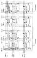
- FIG. 7 shows a configuration example of a memory circuit.
- FIG. 2 shows an example of the configuration of a memory cell.
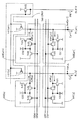
- FIG. 2 shows an example of the configuration of a circuit.
- FIG. 7 shows a structural example of a transistor. The figure which shows energy band structure.
- FIG. 7 shows a structural example of a semiconductor device.
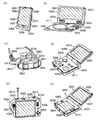
- FIG. 2 shows an example of the configuration of an electronic device.
- FIG. 2 shows an example of the configuration of an electronic device.
- FIG. 2 shows an example of the configuration of an electronic device.
- Embodiment 1 a power feeding device and a non-contact power feeding system which is one embodiment of the present invention will be described with reference to FIGS. 1 to 5.
- the non-contact power feeding system including the power feeding device 100 and the power receiving device 200 will be described as an example of the power feeding device and the non-contact power feeding system of one embodiment of the present invention.
- FIG. 1A shows a block diagram of the power feeding device 100 and the power receiving device 200.
- FIG. 1B is a perspective view of the power supply device 100 and the electronic device 300.
- electronic device 300 is placed on power supply device 100 for charging power storage device 220.
- the electronic device 300 mounts the power receiving device 200.
- the power receiving device 200 has a power receiving coil 210.
- the power feeding device 100 includes a feeding coil 110, an AC power supply 111, a control device 120, a detection device 130, and a moving device 140. Further, as shown in FIG. 1B, the power feeding device 100 includes a casing 150 that encloses the feeding coil 110, the AC power supply 111, the control device 120, the detecting device 130, and the moving device 140.
- the detection device 130 has a function of detecting the position of the power receiving coil 210, and a function of transmitting a detection signal including the result of the detection.
- the control device 120 has a function of determining an optimal position of the feeding coil 110 based on the detection signal, a function of transmitting a position control signal 121 including the position information, and the feeding coil 110 based on the detection signal.
- the moving device 140 has a function of moving the feeding coil 110 to an optimal position as shown by an arrow 101 in FIG. 1B based on the position control signal 121.
- the AC power supply 111 has a function of supplying a voltage to the feed coil 110 based on the output control signal 123.
- the power feeding apparatus 100 can detect the position of the power receiving coil 210 and move the power feeding coil 110 to an optimal position according to the position of the power receiving coil 210, and then feed power to the power receiving coil 210.
- Control device 120 is electrically connected to AC power supply 111, detection device 130, and movement device 140. Further, the control device 120 has a function of receiving the detection signal transmitted from the detection device 130. Further, the control device 120 has a function of determining an optimal position of the feeding coil 110 based on the detection signal, and a function of transmitting a position control signal 121 including the position information to the moving device 140. Further, the control device 120 has a function of transmitting an output control signal 123 for adjusting the size of the output of the feeding coil 110 to the AC power supply 111 in accordance with the detection signal.
- control device 120 may have a function of transmitting an output control signal 123 including information for pausing power feeding.
- Control device 120 may have a full charge detection circuit that detects full charge of power storage device 220 of power reception device 200.
- control device 120 has a function of transmitting to AC power supply 111 an output control signal 123 (hereinafter also referred to as a termination signal) including information for terminating power feeding when full charge of power storage device 220 is detected. It may be done.
- AC power supply 111 is electrically connected to feed coil 110. Further, the AC power supply 111 has a function of receiving the output control signal 123. Further, the AC power supply 111 has a function of supplying a voltage to the feed coil 110 based on the output control signal 123. Further, the AC power supply 111 has a function of temporarily stopping the supply of voltage to the feeding coil 110 based on the output control signal 123.
- the feeding coil 110 has a function of moving by the operation of the moving device 140 and a function of generating a magnetic field by the voltage supplied from the AC power supply 111. Therefore, after the feeding coil 110 moves to the optimal position according to the position of the receiving coil 210, power can be supplied to the receiving coil 210.
- the feed device 100 may have a single feed coil 110 or may have a plurality of feed coils 110. With the power supply device 100 including the plurality of power supply coils 110, power can be supplied to the plurality of power reception devices.
- the sensing device 130 has a plurality of sensing coils.
- the detection device 130 is, for example, a printed circuit board or the like, and the detection coil is constituted by printed wiring formed on the substrate.
- the detection device 130 can also be configured by a substrate and a small coil or chip inductor installed on the substrate. Details of the arrangement method, shape, size, and the like of the detection coil will be described later.
- the detection coil of the detection device 130 has a function of detecting the position of the power reception coil 210 and transmitting a detection signal including the result of the detection to the control device 120.
- the detection of the position of the power reception coil 210 can be performed by detecting a change in magnetic flux density around the detection coil. Note that all of the detection coils of the detection device 130 may have the same function, and part of the detection coil of the detection device 130 and another part of the detection coil of the detection device 130 May have different functions.
- FIG. 1A shows an example in which the detection device 130 includes a detection coil 131 and a detection coil 132 having different functions.
- the detection coil 131 has a function of generating a magnetic field.
- the detection coil 132 has a function of detecting a change in magnetic flux density and transmitting a detection signal to the control device 120.
- the purpose of the detection coil 131 to generate a magnetic field is to detect the position of the power reception coil 210, which is different from the purpose to generate a magnetic field by the feed coil 110. Therefore, it can be said that the maximum value of the strength of the magnetic field generated by the detection coil 131 is smaller than the maximum value of the strength of the magnetic field generated by the feeding coil 110 for power supply.
- a neural network for the control device 120, because it is possible to reliably determine the optimum position of the feeding coil 110 based on complex detection signals.
- the moving device 140 has a function of receiving the position control signal 121 and a function of moving the feeding coil 110 based on the position control signal 121.
- the movement of the feed coil 110 is performed horizontally with the substrate or the like of the detection device 130. Details of the structure of the mobile device 140 will be described later.
- the power receiving device 200 includes a power storage device 220 and a power receiving coil 210. Further, as shown in FIG. 1B, the power receiving device 200 may be mounted on the electronic device 300.
- the power receiving coil 210 has a function of receiving power by the magnetic field generated by the power feeding coil 110 of the power feeding device 100.
- Power storage device 220 is electrically connected to power reception coil 210 and has a function of being charged by the power received by power reception coil 210.
- the detection coils included in the detection device 130 are classified into any one of a first detection coil group to a N-th (N is a natural number of 2 or more) detection coil group. Further, among the detection coils classified into the n-th (n is a natural number of 2 or more and N or less) detection coil group, any one of the detection coils classified into the (n ⁇ 1) th detection coil group Located in the area enclosed by
- the detection device 130 has a detection coil 131 having a function of generating a magnetic field and a detection coil 132 having a function of detecting a change in magnetic flux density and transmitting a detection signal to the control device 120
- a more stable magnetic field can be generated between the detection coils 131 classified into groups.
- the change in magnetic flux density can be detected with higher accuracy between the detection coils 132 classified into the same group. Therefore, with such a configuration, it is possible to improve the detection accuracy of the detection device.
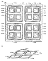
- FIG. 2A shows an example of a top view of the detection device 130. Moreover, in FIG. 2 (B), the perspective view of a part of detection apparatus 130 is shown.
- FIG. 2 shows an example in which the detection coil of the detection device 130 is classified into any one of the first coil group and the second detection coil group. Further, in FIG. 2, the detection device 130 has a detection coil 131 having a function of generating a magnetic field, and a detection coil 132 having a function of detecting a change in magnetic flux density and transmitting a detection signal to the control device 120.
- a detection coil 131 having a function of generating a magnetic field
- a detection coil 132 having a function of detecting a change in magnetic flux density and transmitting a detection signal to the control device 120.
- the detection device 130 illustrated in FIG. 2A includes a substrate 135, two detection coils 131a, two detection coils 132a, eight detection coils 131b, and eight detection coils 132b. .
- the detection coil 131a, the detection coil 132a, the detection coil 131b, and the detection coil 132b are printed wiring formed on the substrate 135.
- detection coils 131a and 132a are shown as specific examples of the detection coils belonging to the first detection coil group.
- the detection coil 131b and the detection coil 132b are shown as a specific example of the detection coil which belongs to a 2nd detection coil group.
- detection coils 131a and 131b are shown.
- detection coil 132a and a detection coil 132b are shown.
- the detection coil 131a and the detection coil 132a have the same size. Also, two detection coils 131a and two detection coils 132a are located in the area 133a.
- the size is equal to the detection coil 131b and the detection coil 132b.
- the detection coil 131b and the detection coil 132b are smaller in size than the detection coil 131a and the detection coil 132a.
- the two detection coils 131 b and the two detection coils 132 b are located in a region 133 b surrounded by either the detection coil 131 a or the detection coil 132 a.
- the detection device 130 may have a detection coil located in a region 133c (see FIG. 2A) surrounded by any one of the detection coil 131b or the detection coil 132b. For example, by providing four detection coils in the region 133c, the change in magnetic flux density can be detected in more detail, which is preferable.
- the two detection coils 131a are arranged so as not to be adjacent to each other. Further, the two detection coils 132a are arranged not to be adjacent to each other. In addition, the two detection coils 131 b are disposed so as not to be adjacent to each other. In addition, the two detection coils 132b are arranged not to be adjacent to each other.
- FIG. 2B is a perspective view of the region 133a and the detection coil 131a and the detection coil 132a located in the region 133a. Further, FIG. 2B shows an arrow 137 expressing a magnetic field that can be generated between the two detection coils 131a.
- FIG. 2A it is possible to generate a stable magnetic field between the two detection coils 131a. Also, similarly, it becomes possible to generate a stable magnetic field between the two detection coils 131b.
- the configuration of the detection device 130 is not particularly limited to the configuration shown in FIG.
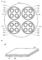
- FIG. 3A a top view of a modification of the detection device 130 is shown.
- a modification of the detection device 130 shown in FIG. 3A includes a circular substrate 135, a circular detection coil 131a, a circular detection coil 132a, a circular detection coil 131b, and a circular detection coil 132b. Have.
- FIG. 3B a perspective view of a detection device 136 which is a modification of the detection device 130 is shown.
- the sensing device 136 includes a sensing device 130a, a dielectric 138, and a sensing device 130b.
- the detection device 130a and the detection device 130b are arranged to overlap with each other.
- the dielectric 138 is disposed at a position where it is sandwiched between the sensing device 130a and the sensing device 130b.
- the detection device 130 a and the detection device 130 b may each have the same configuration as the detection device 130 illustrated in FIG. 2.
- the magnetic flux density can be detected three-dimensionally, which is preferable.
- the distance between the detection device 136 and the power reception coil 210 can be easily detected when the power reception device 200 having the power reception coil 210 is brought close to the power supply device 100, which is preferable.
- FIG. 4A shows a perspective view of an example of the moving device 140. Further, FIG. 4B shows another example of the mobile device 140.
- the moving device 140 shown in FIG. 4A includes two rails 141, one rail 142, and one coil base 143.
- the rail 142 can move smoothly on the rail 141.
- the coil base 143 can move smoothly on the rail 142.
- the coil base 143 also has a tire 144 driven by an electronic motor. Moreover, it is possible to attach the feed coil 110 on the coil base.
- the moving device 140 can move the feeding coil 110 horizontally with the substrate or the like included in the detecting device 130.
- the moving device 140 shown in FIG. 4B includes two rails 141, two rails 142, and two coil bases 143. With such a configuration, the moving device 140 may move the plurality of feed coils 110.
- the above is a detailed description of the mobile device 140.
- the configuration of the mobile device 140 is not limited to the configuration shown in FIG.
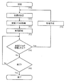
- FIG. 5 shows a flowchart for explaining the power supply method of the power supply apparatus 100.
- the power receiving device 200 is placed on the power feeding device 100, and the power feeding device 100 starts operation (see FIG. 5 (T0)).
- the optimum feed coil position is determined (see FIG. 5 (T1)). As described above, the determination of the optimal position of the feeding coil 110 can be performed by processing the detection signal transmitted from the detection device 130 in the control device 120.
- Second step In the second step, the feeding coil 110 is moved (see FIG. 5 (T2)). As described above, the moving device 140 has the function of moving the feeding coil 110.
- ⁇ 3rd step >> In the third step, power feeding is started (see FIG. 5 (T3)). As described above, the feeding coil 110 has a function of inducing an electromotive force.
- ⁇ 4th step it is determined whether or not the power receiving coil 210 has moved (see FIG. 5 (T4)). If it is determined that the power receiving coil 210 has moved to a position different from the position at the start of power feeding, the process proceeds to the fifth step, and if it is determined that the power receiving coil 210 has not moved from the position at the power feeding start Proceed to the sixth step.
- the movement of the power receiving coil 210 is assumed to occur, for example, due to vibration of the power receiving device 200 having the power receiving coil 210.
- ⁇ 5th step the power supply apparatus 100 pauses power feeding, and then proceeds to the first step (see FIG. 5 (T5)).
- the operation method of the power supply apparatus 100 is not limited to temporarily stopping power supply.
- the operation may be performed such that the power supply is continued after reducing the output, or after the fourth step, the process may proceed to the first step without passing through the fifth step.
- Such control of the output of the feeding coil 110 can be performed by the output control signal 123 transmitted from the control device 120 to the AC power supply 111.
- ⁇ 6th step when the AC power supply 111 receives the termination signal, power supply is terminated, and when the AC power supply 111 does not receive the termination signal, the process proceeds to the fourth step (see (T6) in FIG. 5). ).
- the end signal is transmitted from the control device 120, for example, when the power receiving device 200 is separated from the power feeding device, or when the power storage device 220 of the power receiving device 200 is fully charged.
- the above is the power feeding method of the power feeding device 100.
- artificial intelligence is a generic term of the computer which imitated human intelligence.
- artificial intelligence includes artificial neural networks (ANN).
- An artificial neural network is a circuit that simulates a neural network composed of neurons and synapses.
- the term "neural network” as used herein refers particularly to artificial neural networks.
- the control device 120 shown in FIG. 6 has a position control circuit 122 and an output control circuit 124.
- the position control circuit 122 and the output control circuit 124 each have a function to which a detection signal transmitted by the detection device 130 is supplied. Further, the position control circuit 122 has a function of transmitting the position control signal 121. The position control circuit 122 also includes a neural network NN. The output control circuit 124 also has a function of transmitting the output control signal 123.
- the neural network NN has an input layer IL, an output layer OL, and a hidden layer (intermediate layer) HL. Detection information acquired by the detection device 130 is input to the input layer IL.
- Each of the output layer OL, the input layer IL, and the hidden layer HL has one or more units (neuron circuits), and the output of each unit is supplied to units provided in different layers through weights (coupling strength). Be done.
- the number of units in each layer can be set arbitrarily.
- the neural network NN may be a network (DNN: deep neural network) having a plurality of hidden layers HL. The learning of deep neural networks is sometimes called deep learning.
- the neural network NN is added with a function of determining the optimum position of the feed coil 110 based on the detection information by learning. Then, when data corresponding to the detection information is input to the input layer of the neural network NN, arithmetic processing is performed in each layer. Arithmetic processing in each layer is performed by a product-sum operation of an output of a unit in the previous layer and a weighting factor.
- the bonding between layers may be a total bond in which all units are bonded, or a partial bond in which some units are bonded. Then, data corresponding to the result of determining the optimum position of the feeding coil 110 is output from the output layer OL.
- the neural network NN for the position control circuit 122, it is possible to more easily and accurately determine the optimum position of the feeding coil 110 based on the detection signal.
- the neural network is composed of a neuron circuit NC and a synapse circuit SC provided between the neuron circuits NC.
- FIG. 7A shows a configuration example of the neuron circuit NC and the synapse circuit SC.
- Input data x 1 to x L (L is a natural number) are input to the synapse circuit SC.
- the synapse circuit SC has a function of storing a weighting coefficient w k (k is an integer of 1 or more and L or less). Weight coefficient w k corresponds to the strength of coupling between neuron circuits NC.
- the neuron circuit NC When the input data x 1 to x L is input to the synapse circuit SC, the product of the input data x k input to the synapse circuit SC and the weight coefficient w k stored in the synapse circuit SC is input to the neuron circuit NC.
- a value (x 1 w 1 + x 2 w 2 +... + X L w L ) obtained by adding (x k w k ) for k 1 to L , that is, obtained by a product-sum operation using x k and w k
- the supplied value is supplied.
- this value exceeds the threshold ⁇ of the neuron circuit NC, the neuron circuit NC outputs a high level signal. This phenomenon is called firing of the neuron circuit NC.
- FIG. 7 (B) A model of a hierarchical neural network using the above-described neuron circuit NC and synapse circuit SC is shown in FIG. 7 (B).
- the neural network has an input layer IL, a hidden layer HL, and an output layer OL.
- the input layer IL has an input neuron circuit IN.
- the hidden layer HL has a hidden synapse circuit HS and a hidden neuron circuit HN.
- the output layer OL has an output synapse circuit OS and an output neuron circuit ON.
- threshold values ⁇ of the input neuron circuit IN, the hidden neuron circuit HN, and the output neuron circuit ON are denoted as ⁇ I , ⁇ H , and ⁇ O , respectively.
- Data x 1 to x i (i is a natural number) corresponding to the detection signal is supplied to the input layer IL, and the output of the input layer IL is supplied to the hidden layer HL. Then, the value obtained by the product-sum operation using the output data of the input layer IL and the weighting factor w held in the hidden synapse circuit HS is supplied to the hidden neuron circuit HN. Then, the output neuron circuit ON is supplied with the output of the hidden neuron circuit HN and the value obtained by the product-sum operation using the weight coefficient w held in the output synapse circuit OS. Then, data y corresponding to the optimal position of the feeding coil 110 is output.
- the neural network shown in FIG. 7B has a function of determining the optimal position of the feeding coil 110 based on the detection information.
- FIG. 7C shows a model of a neural network that performs supervised learning using an error back propagation method.
- the error back propagation method is one of the methods of changing the weight coefficient of the synapse circuit so that the error between the output data of the neural network and the teacher data becomes small.
- the error [delta] O which is determined based on the output data (data y) and teacher data (data t) are changed weighting coefficient w of the hidden synapse circuit HS.
- the weighting factor w of the previous stage synapse circuit SC is modified in accordance with the amount of modification of the weighting factor w of the hidden synapse circuit HS.
- learning of the neural network NN can be performed by sequentially changing the weight coefficient of the synapse circuit SC based on the teacher data.
- the number of hidden layers HL may be two or more. In this way, deep learning can be performed.
- Embodiment 2 a structural example of a semiconductor device which can be used for the neural network described in Embodiment 2 will be described.
- the product-sum operation in the neural network can be performed using a product-sum operation element.
- a configuration example of a semiconductor device that can be used as a product-sum operation element of the neural network NN will be described.
- FIG. 8 An example of the configuration of the semiconductor device 500 is shown in FIG.
- the semiconductor device 500 illustrated in FIG. 8 includes a memory circuit 510 (MEM), a reference memory circuit 520 (RMEM), a circuit 530, and a circuit 540.
- the semiconductor device 500 may further include a current source circuit 550 (CREF).
- MEM memory circuit 510
- RMEM reference memory circuit 520
- CREF current source circuit 550
- the memory circuit 510 has a memory cell MC [p, q] and a memory cell MC exemplified by the memory cell MC [p + 1, q].
- Each memory cell MC has an element having a function of converting an input potential to a current.
- an active element such as a transistor can be used, for example.
- FIG. 8 exemplifies the case where each memory cell MC includes the transistor Tr11.
- the first analog potential is input to the memory cell MC from the wiring WD exemplified by the wiring WD [q].
- the first analog potential corresponds to first analog data.
- the memory cell MC has a function of generating a first analog current according to the first analog potential. Specifically, the drain current of the transistor Tr11 obtained when the first analog potential is supplied to the gate of the transistor Tr11 can be used as the first analog current.
- the current flowing to the memory cell MC [p, q] is I [p, q]
- the current flowing to the memory cell MC [p + 1, q] is I [p + 1, q].
- the transistor Tr11 when the transistor Tr11 operates in a saturation region, its drain current does not depend on the voltage between the source and the drain but is controlled by the difference between the gate voltage and the threshold voltage. Therefore, it is desirable to operate the transistor Tr11 in the saturation region. In order to operate the transistor Tr11 in the saturation region, it is assumed that the gate voltage and the voltage between the source and the drain are appropriately set to voltages in the range of operation in the saturation region.
- the potential according to] is input.
- the memory cell MC [p, q] has a function of generating a first analog current according to the first analog potential Vx [p, q]. That is, in this case, the current I [p, q] of the memory cell MC [p, q] corresponds to the first analog current.
- the first analog potential Vx [p + 1, q] or the first analog potential Vx [p + 1] from the wiring WD [q] to the memory cell MC [p + 1, q]. , Q] are input.
- the memory cell MC [p + 1, q] has a function of generating a first analog current according to the first analog potential Vx [p + 1, q]. That is, in this case, the current I [p + 1, q] of the memory cell MC [p + 1, q] corresponds to the first analog current.
- the memory cell MC has a function of holding the first analog potential. That is, it can be said that the memory cell MC has a function of holding the first analog current according to the first analog potential by holding the first analog potential.
- the second analog potential is input to the memory cell MC from the wiring RW exemplified by the wiring RW [p] and the wiring RW [p + 1].
- the second analog potential corresponds to second analog data.
- Memory cell MC has a function of adding the second analog potential or a potential corresponding to the second analog potential to the already held first analog potential, and a third analog potential obtained by adding And a function to hold.
- the memory cell MC has a function of generating a second analog current according to the third analog potential. That is, it can be said that the memory cell MC has a function of holding the second analog current according to the third analog potential by holding the third analog potential.
- the second analog potential Vw [p, q] is input to the memory cell MC [p, q] from the wiring RW [p].
- the memory cell MC [p, q] has a function of holding a third analog potential corresponding to the first analog potential Vx [p, q] and the second analog potential Vw [p, q].
- the memory cell MC [p, q] has a function of generating a second analog current according to the third analog potential. That is, in this case, the current I [p, q] of the memory cell MC [p, q] corresponds to the second analog current.
- the second analog potential Vw [p + 1, q] is input to the memory cell MC [p + 1, q] from the wiring RW [p + 1].
- the memory cell MC [p + 1, q] has a function of holding a third analog potential corresponding to the first analog potential Vx [p + 1, q] and the second analog potential Vw [p + 1, q].
- the memory cell MC [p + 1, q] has a function of generating a second analog current according to the third analog potential. That is, in this case, the current I [p + 1, q] of the memory cell MC [p + 1, q] corresponds to the second analog current.
- the current I [p, q] flows between the wiring BL [q] and the wiring VR [q] through the memory cell MC [p, q].
- the current I [p + 1, q] flows between the wiring BL [q] and the wiring VR [q] via the memory cell MC [p + 1, q]. Therefore, the current I [q] corresponding to the sum of the current I [p, q] and the current I [p + 1, q] passes through the memory cell MC [p, q] and the memory cell MC [p + 1, q]. It flows between the wiring BL [q] and the wiring VR [q].
- the reference storage circuit 520 has a memory cell MCR [p] and a memory cell MCR exemplified by the memory cell MCR [p + 1].
- the first reference potential VPR is input to the memory cell MCR from the wiring WDREF.
- the memory cell MCR has a function of generating a first reference current according to the first reference potential VPR.
- the current flowing to the memory cell MCR [p] is IREF [p]
- the current flowing to the memory cell MCR [p + 1] is IREF [p + 1].
- the first reference potential VPR is input to the memory cell MCR [p] from the wiring WDREF.
- the memory cell MCR [p] has a function of generating a first reference current according to the first reference potential VPR. That is, in this case, the current IREF [p] of the memory cell MCR [p] corresponds to the first reference current.
- the first reference potential VPR is input to the memory cell MCR [p + 1] from the wiring WDREF.
- the memory cell MCR [p + 1] has a function of generating a first reference current according to the first reference potential VPR. That is, in this case, the current IREF [p + 1] of the memory cell MCR [p + 1] corresponds to the first reference current.
- the memory cell MCR has a function of holding the first reference potential VPR. That is, it can be said that the memory cell MCR has a function of holding the first reference current corresponding to the first reference potential VPR by holding the first reference potential VPR.
- the second analog potential is input to the memory cell MCR from the wiring RW illustrated by the wiring RW [p] and the wiring RW [p + 1].
- Memory cell MCR has a function of adding the second analog potential or a potential corresponding to the second analog potential to the already held first reference potential VPR, and a second reference potential obtained by addition. Have the ability to hold The memory cell MCR has a function of generating a second reference current according to the second reference potential. That is, it can be said that the memory cell MCR has a function of holding the second reference current according to the second reference potential by holding the second reference potential.
- the second analog potential Vw [p, q] is input to the memory cell MCR [p] from the wiring RW [p].
- the memory cell MCR [p] has a function of holding a second reference potential corresponding to the first reference potential VPR and the second analog potential Vw [p, q].
- the memory cell MCR [p] has a function of generating a second reference current according to the second reference potential. That is, in this case, the current IREF [p] of the memory cell MCR [p] corresponds to the second reference current.
- the second analog potential Vw [p + 1, q] is input to the memory cell MCR [p + 1] from the wiring RW [p + 1].
- the memory cell MCR [p + 1] has a function of holding a second reference potential corresponding to the first reference potential VPR and the second analog potential Vw [p + 1, q].
- the memory cell MCR [p + 1] has a function of generating a second reference current according to the second reference potential. That is, in this case, the current IREF [p + 1] of the memory cell MCR [p + 1] corresponds to the second reference current.
- the current IREF [p] flows between the wiring BLREF and the wiring VRREF through the memory cell MCR [p].
- the current IREF [p + 1] flows between the wiring BLREF and the wiring VRREF through the memory cell MCR [p + 1]. Therefore, a current IREF corresponding to the sum of the current IREF [p] and the current IREF [p + 1] flows between the wiring BLREF and the wiring VRREF through the memory cell MCR [p] and the memory cell MCR [p + 1]. Become.
- the current source circuit 550 has a function of supplying, to the wiring BL, a current having the same value as the current IREF flowing to the wiring BLREF, or a current corresponding to the current IREF. Then, when setting an offset current to be described later, the current flowing between the wiring BL [q] and the wiring VR [q] via the memory cell MC [p, q] and the memory cell MC [p + 1, q] When I [q] is different from the current IREF flowing between the wiring BLREF and the wiring VRREF through the memory cell MCR [p] and the memory cell MCR [p + 1], a differential current flows in the circuit 530 or the circuit 540. Circuit 530 has a function as a current source circuit, and circuit 540 has a function as a current sink circuit.
- the circuit 530 when the current I [q] is larger than the current IREF, the circuit 530 has a function of generating a current ⁇ I [q] corresponding to the difference between the current I [q] and the current IREF.
- the circuit 530 also has a function of supplying the generated current ⁇ I [q] to the wiring BL [q]. That is, it can be said that the circuit 530 has a function of holding the current ⁇ I [q].
- the circuit 540 When the current I [q] is smaller than the current IREF, the circuit 540 has a function of generating a current ⁇ I [q] corresponding to the difference between the current I [q] and the current IREF. The circuit 540 also has a function of drawing the generated current ⁇ I [q] from the wiring BL [q]. That is, it can be said that the circuit 540 has a function of holding the current ⁇ I [q].
- a potential corresponding to the first analog potential is stored in the memory cell MC [p, q].
- the potential VPR-Vx [p, q] obtained by subtracting the first analog potential Vx [p, q] from the first reference potential VPR is the memory cell MC [p] via the wiring WD [q]. , Q].
- the potential VPR-Vx [p, q] is held.
- a current I [p, q] corresponding to the potential VPR ⁇ Vx [p, q] is generated.
- the first reference potential VPR is a high level potential higher than the ground potential. Specifically, it is desirable that the potential is higher than the ground potential and equal to or less than the high level potential VDD supplied to the current source circuit 550.
- the first reference potential VPR is stored in the memory cell MCR [p]. Specifically, the first reference potential VPR is input to the memory cell MCR [p] through the wiring WDREF. The memory cell MCR [p] holds the first reference potential VPR. In memory cell MCR [p], a current IREF [p] corresponding to the first reference potential VPR is generated.
- a potential corresponding to the first analog potential is stored in the memory cell MC [p + 1, q].
- the potential VPR-Vx [p + 1, q] obtained by subtracting the first analog potential Vx [p + 1, q] from the first reference potential VPR is the memory cell MC [p + 1] through the wiring WD [q]. , Q].
- the potential VPR-Vx [p + 1, q] is held.
- a current I [p + 1, q] corresponding to the potential VPR-Vx [p + 1, q] is generated.
- the first reference potential VPR is stored in the memory cell MCR [p + 1]. Specifically, the first reference potential VPR is input to the memory cell MCR [p + 1] through the wiring WDREF. Memory cell MCR [p + 1] holds first reference potential VPR. Further, in the memory cell MCR [p + 1], the current IREF [p + 1] corresponding to the first reference potential VPR is generated.
- the wiring RW [p] and the wiring RW [p + 1] are set to the reference potential.
- a ground potential, a low level potential VSS lower than the ground potential, or the like can be used as the reference potential.
- the potential of the wiring RW can be made higher than the ground potential even if the second analog potential Vw is positive or negative, so that signal generation can be facilitated. Is preferable because it enables product operations on positive or negative analog data.
- a current obtained by combining currents respectively generated in the memory cells MC connected to the wiring BL [q] flows in the wiring BL [q].
- the current I [p, q] generated in the memory cell MC [p, q] and the current I [p + 1, q] generated in the memory cell MC [p + 1, q] are combined.
- Current I [q] flows.
- a current obtained by combining currents respectively generated in the memory cells MCR connected to the wiring BLREF flows in the wiring BLREF.
- a current IREF which is a combination of the current IREF [p] generated in the memory cell MCR [p] and the current IREF [p + 1] generated in the memory cell MCR [p + 1] flows.
- the current I [q] obtained by inputting the first analog potential and the first reference potential are input.
- the offset current Ioffset [q] obtained from the difference with the obtained current IREF is held in the circuit 530 or the circuit 540.
- the circuit 530 supplies the current Ioffset [q] to the wiring BL [q]. That is, the current ICM [q] flowing through the circuit 530 corresponds to the current Ioffset [q]. Then, the value of the current ICM [q] is held in the circuit 530.
- the circuit 540 draws the current Ioffset [q] from the wiring BL [q]. That is, the current ICP [q] flowing through the circuit 540 corresponds to the current Ioffset [q]. Then, the value of the current ICP [q] is held in the circuit 540.
- the second analog potential or the second analog potential it is added to the first analog potential or the potential corresponding to the first analog potential already held in the memory cell MC [p, q].
- the potential is stored in the memory cell MC [p, q].
- the second analog potential Vw [p] is stored in memory via the wiring RW [p] by setting the potential of the wiring RW [p] higher than the reference potential by Vw [p]. It is input to the cell MC [p, q].
- the potential VPR-Vx [p, q] + Vw [p] is held.
- a current I [p, q] corresponding to the potential VPR ⁇ Vx [p, q] + Vw [p] is generated.
- the second analog potential or the second analog potential it is added to the first analog potential or the potential corresponding to the first analog potential already held in the memory cell MC [p + 1, q].
- the potential is stored in the memory cell MC [p + 1, q].
- the second analog potential Vw [p + 1] can be stored in memory via the wiring RW [p + 1]. It is input to the cell MC [p + 1, q].
- the potential VPR-Vx [p + 1, q] + Vw [p + 1] is held.
- a current I [p + 1, q] corresponding to the potential VPR-Vx [p + 1, q] + Vw [p + 1] is generated.
- the potential of the wiring RW [p] is Vw [p] and the potential of the wiring RW [p + 1] is Vw [p + 1]
- the second analog current is expressed by the following equation 1.
- k is a coefficient
- Vth is a threshold voltage of the transistor Tr11.
- the second reference current is represented by the following formula 2.
- Equation 1 The current ⁇ I [q] is derived from Equation 1, Equation 2 and Equation 3 as Equation 4 below.
- Equation 4 the term represented by 2k ⁇ i (Vw [p] ⁇ Vx [p, q]) is the product of the first analog potential Vx [p, q] and the second analog potential Vw [p] and This corresponds to the sum of the product of one analog potential Vx [p + 1, q] and the second analog potential Vw [p + 1].
- the current Ioffset [q] is set such that the second analog potential Vw [p] is 0 and the second analog potential Vw [p + 1] is 0 when all the potentials of the wiring RW [p] are the reference potential. Assuming that the current ⁇ I [q] at that time, Equation 5 below is derived from Equation 4.
- the current Iout [q] is 2k ⁇ i (Vw [p] ⁇ Vx [p, q]), and the first analog potential Vx [p, q] and the second analog potential Vw [p] It can be seen that it corresponds to the sum of the product and the product of the first analog potential Vx [p + 1, q] and the second analog potential Vw [p + 1].
- the transistor Tr11 can be regarded as operating in the saturation region.
- arithmetic processing of analog data can be performed without conversion to digital data, so that the circuit scale of the semiconductor device can be reduced.
- arithmetic processing of analog data can be executed without conversion to digital data, so that time required for arithmetic processing of analog data can be suppressed.
- low power consumption of a semiconductor device can be realized while suppressing a time required for arithmetic processing of analog data.
- the memory circuit 510 has a plurality of memory cells MC in y rows x columns (x and y are natural numbers), and the reference memory circuit 520 (RMEM) has a plurality of memory cells in y rows and 1 column. The case where it has MCR is illustrated.
- a source of a transistor means a source region which is part of a semiconductor layer functioning as a channel formation region, a source electrode connected to the semiconductor layer, or the like.
- the drain of the transistor means a drain region which is part of the semiconductor layer, a drain electrode connected to the semiconductor layer, or the like.
- the gate means a gate electrode or the like.
- the names of the source and the drain of the transistor are switched depending on the conductivity type of the transistor and the level of the potential supplied to each terminal.
- a terminal to which a low potential is applied is called a source
- a terminal to which a high potential is applied is called a drain
- a terminal to which a high potential is applied is called a source.
- the connection relationship of transistors may be described on the assumption that the source and the drain are fixed for convenience, but in actuality, the name of the source and the drain is referred to according to the relationship of the above-mentioned potentials. Replace.
- the memory circuit 510 is connected to the wiring RW, the wiring WW, the wiring WD, the wiring VR, and the wiring BL.
- wirings RW [1] to RW [y] are connected to memory cells MC in each row, and wirings WW [1] to WW [y] are connected to memory cells MC in each row, and wiring WD [1] to the wiring WD [x] are connected to the memory cells MC of the respective columns, and the wirings BL [1] to the wiring BL [x] are respectively connected to the memory cells MC of the respective columns.
- FIG. 9 exemplifies the case where the wirings VR [1] to VR [x] are connected to the memory cells MC in the respective columns. Note that the wirings VR [1] to VR [x] may be connected to each other.
- the reference memory circuit 520 is connected to the wiring RW, the wiring WW, the wiring WDREF, the wiring VRREF, and the wiring BLREF.
- wirings RW [1] to RW [y] are connected to memory cells MCR in each row
- wirings WW [1] to WW [y] are connected to memory cells MCR in each row
- wiring WDREF Are respectively connected to the memory cells MCR in one column
- the wiring BLREF is connected to the memory cells MCR in one column
- the wiring VRREF is connected to the memory cells MCR in one column.
- the wiring VRREF may be connected to the wirings VR [1] to VR [x].
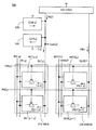
- FIG. 10 illustrates the memory cell MCR [p] in the p-th row and the memory cell MCR [p + 1] in the p + 1-th row.
- p and p + 1 are each an arbitrary number from 1 to y
- q and q + 1 are each an arbitrary number from 1 to x.
- the memory cell MC [p, q] in the p-th row, the memory cell MC [p, q + 1], and the memory cell MCR [p] are connected to the wiring RW [p] and the wiring WW [p]. Also, the memory cell MC [p + 1, q] in the (p + 1) th row, the memory cell MC [p + 1, q + 1], and the memory cell MCR [p + 1] are connected to the wiring RW [p + 1] and the wiring WW [p + 1]. There is.
- the memory cell MC [p, q] in the q-th column and the memory cell MC [p + 1, q] are connected to the wiring WD [q], the wiring VR [q], and the wiring BL [q].
- the memory cell MC [p, q + 1] in the q + 1 th column and the memory cell MC [p + 1, q + 1] are connected to the wiring WD [q + 1], the wiring VR [q + 1], and the wiring BL [q + 1]. .
- the memory cell MCR [p] in the p-th row and the memory cell MCR [p + 1] in the p + 1-th row are connected to the wiring WDREF, the wiring VRREF, and the wiring BLREF.
- Each memory cell MC and each memory cell MCR have a transistor Tr11, a transistor Tr12, and a capacitive element C11.
- the transistor Tr12 has a function of controlling the input of the first analog potential to the memory cell MC or the memory cell MCR.
- the transistor Tr11 has a function of generating an analog current in accordance with the potential input to the gate.
- Capacitive element C11 sets the second analog potential or the second analog potential to a potential corresponding to the first analog potential or the first analog potential held in memory cell MC or memory cell MCR. It has a function to add.
- the gate of the transistor Tr12 is connected to the wiring WW, one of the source or drain is connected to the wiring WD, and the other of the source or drain is connected to the gate of the transistor Tr11. ing.
- the transistor Tr11 one of the source and the drain is connected to the wiring VR, and the other of the source or the drain is connected to the wiring BL.
- the first electrode of the capacitor C11 is connected to the wiring RW, and the second electrode is connected to the gate of the transistor Tr11.
- the gate of the transistor Tr12 is connected to the wiring WW, one of the source or drain is connected to the wiring WDREF, and the other of the source or drain is connected to the gate of the transistor Tr11. .
- the transistor Tr11 one of the source and the drain is connected to the wiring VRREF, and the other of the source or the drain is connected to the wiring BLREF.
- the first electrode of the capacitor C11 is connected to the wiring RW, and the second electrode is connected to the gate of the transistor Tr11.
- the first analog potential is input to the node N via the transistor Tr12, and then the node N becomes floating when the transistor Tr12 is turned off.
- a potential corresponding to the first analog potential or the first analog potential is held at node N.
- the second analog potential input to the first electrode of the capacitive element C11 is applied to the node N.
- the amount of change in the potential of the first electrode is reflected as it is on the amount of change in the potential of node N
- the amount of change in the potential of the first electrode is multiplied by the coupling coefficient uniquely determined from the capacitance value of the capacitive element C11, the capacitance value of the gate capacitance of the transistor Tr11, and the capacitance value of the parasitic capacitance.
- the amount of change in the potential of the node N can be accurately calculated.
- the amount of change in the potential of the first electrode is substantially reflected in the amount of change in the potential of the node N.
- the drain current of the transistor Tr11 is determined according to the potential of the node N. Therefore, when the potential of the node N is held as the transistor Tr12 is turned off, the value of the drain current of the transistor Tr11 is also held.
- the drain current reflects the first analog potential and the second analog potential.
- node NREF In memory cell MCR, assuming that the gate of transistor Tr11 is node NREF, in memory cell MCR, the first reference potential or a potential corresponding to the first reference potential is input to node NREF through transistor Tr12, and then the transistor When the transistor Tr12 is turned off, the node NREF is in a floating state, and the node NREF holds the first reference potential or a potential corresponding to the first reference potential.
- the second analog potential input to the first electrode of the capacitive element C11 is applied to the node NREF.
- node NREF is a potential obtained by adding the second analog potential or the potential corresponding to the second analog potential to the first reference potential or the potential corresponding to the first reference potential. Become.
- the drain current of transistor Tr11 is determined according to the potential of node NREF. Therefore, when the potential of the node NREF is held by the transistor Tr12 being turned off, the value of the drain current of the transistor Tr11 is also held.
- the drain current reflects the first reference potential and the second analog potential.
- a drain current flowing to the transistor Tr11 of the memory cell MC [p, q] is a current I [p, q]
- a drain current flowing to the transistor Tr11 of the memory cell MC [p + 1, q] is a current I [p + 1, q].
- the sum of the currents supplied from the wiring BL [q] to the memory cell MC [p, q] and the memory cell MC [p + 1, q] is a current I [q].
- the drain current flowing to the transistor Tr11 of the memory cell MC [p, q + 1] is current I [p, q + 1]
- the drain current flowing to the transistor Tr11 of the memory cell MC [p + 1, q + 1] is current I [p + 1, q + 1].
- the sum of the currents supplied from the wiring BL [q + 1] to the memory cell MC [p, q + 1] and the memory cell MC [p + 1, q + 1] is a current I [q + 1].
- the drain current flowing to the transistor Tr11 of the memory cell MCR [p] is a current IREF [p]
- the drain current flowing to the transistor Tr11 of the memory cell MCR [p + 1] is a current IREF [p + 1]
- the memory cell The sum of the currents supplied to MCR [p] and the memory cell MCR [p + 1] is the current IREF.
- FIG. 11 shows an example of the configuration of the circuit 530, the circuit 540, and the current source circuit 550 corresponding to the memory cell MC and the memory cell MCR shown in FIG.
- the circuit 530 illustrated in FIG. 11 includes a circuit 530 [q] corresponding to the qth memory cell MC and a circuit 530 [q + 1] corresponding to the q + 1th memory cell MC.
- the circuit 540 shown in FIG. 11 has a circuit 540 [q] corresponding to the qth memory cell MC and a circuit 540 [q + 1] corresponding to the q + 1th memory cell MC.
- the circuit 530 [q] and the circuit 540 [q] are connected to the wiring BL [q].
- the circuit 530 [q + 1] and the circuit 540 [q + 1] are connected to the wiring BL [q + 1].
- the current source circuit 550 is connected to the wiring BL [q], the wiring BL [q + 1], and the wiring BLREF.
- the current source circuit 550 has a function of supplying the current IREF to the wiring BLREF, and a function of supplying the same current as the current IREF or a current corresponding to the current IREF to the wiring BL [q] and the wiring BL [q + 1]. Have.
- the circuits 530 [q] and 530 [q + 1] each include transistors Tr24 to Tr26 and a capacitor C22.
- the transistor Tr24 When setting the offset current, in the circuit 530 [q], the transistor Tr24 generates a current ICM [corresponding to the difference between the current I [q] and the current IREF when the current I [q] is larger than the current IREF. q] is generated.
- the transistor Tr24 In the circuit 530 [q + 1], the transistor Tr24 has a function of generating a current ICM [q + 1] corresponding to the difference between the current I [q + 1] and the current IREF when the current I [q + 1] is larger than the current IREF. Have.
- the current ICM [q] and the current ICM [q + 1] are supplied from the circuit 530 [q] and the circuit 530 [q + 1] to the wiring BL [q] and the wiring BL [q + 1].
- one of the source and the drain of the transistor Tr24 is connected to the corresponding wiring BL, and the other of the source or the drain is a wiring to which a predetermined potential is supplied. It is connected.
- One of the source and the drain of the transistor Tr25 is connected to the wiring BL, and the other of the source and the drain is connected to the gate of the transistor Tr24.
- the transistor Tr26 one of the source and the drain is connected to the gate of the transistor Tr24, and the other of the source and the drain is connected to a wiring to which a predetermined potential is supplied.
- a first electrode of the capacitive element C22 is connected to the gate of the transistor Tr24, and a second electrode of the capacitive element C22 is connected to a wiring to which a predetermined potential is supplied.
- the gate of the transistor Tr25 is connected to the wiring OSM, and the gate of the transistor Tr26 is connected to the wiring ORM.
- FIG. 11 illustrates the case where the transistor Tr24 is a p-channel type and the transistors Tr25 and Tr26 are an n-channel type.
- the circuit 540 [q] and the circuit 540 [q + 1] each include transistors Tr21 to Tr23 and a capacitor C21.
- the transistor Tr21 is a current ICP [corresponding to the difference between the current I [q] and the current IREF when the current I [q] is smaller than the current IREF. q] is generated.
- the transistor Tr21 has a function of generating a current ICP [q + 1] corresponding to the difference between the current I [q + 1] and the current IREF when the current I [q + 1] is smaller than the current IREF.
- the current ICP [q] and the current ICP [q + 1] are drawn from the wiring BL [q] and the wiring BL [q + 1] to the circuit 540 [q] and the circuit 540 [q + 1].
- the current ICM [q] and the current ICP [q] correspond to the current Ioffset [q].
- the current ICM [q + 1] and the current ICP [q + 1] correspond to the current Ioffset [q + 1].
- one of the source and the drain of the transistor Tr21 is connected to the corresponding wiring BL, and the other of the source or the drain is a wiring to which a predetermined potential is supplied. It is connected.
- One of the source and the drain of the transistor Tr22 is connected to the wiring BL, and the other of the source and the drain is connected to the gate of the transistor Tr21.
- the transistor Tr23 one of the source and the drain is connected to the gate of the transistor Tr21, and the other of the source and the drain is connected to a wiring to which a predetermined potential is supplied.
- the first electrode of the capacitive element C21 is connected to the gate of the transistor Tr21, and the second electrode is connected to a wiring to which a predetermined potential is supplied.
- the gate of the transistor Tr22 is connected to the wiring OSP, and the gate of the transistor Tr23 is connected to the wiring ORP.
- FIG. 11 illustrates the case where the transistors Tr21 to Tr23 are n-channel transistors.
- the current source circuit 550 further includes a transistor Tr27 corresponding to the wiring BL and a transistor Tr28 corresponding to the wiring BLREF. Specifically, in the case where the current source circuit 550 shown in FIG. 11 includes the transistor Tr27 [q] corresponding to the wiring BL [q] and the transistor Tr27 [q + 1] corresponding to the wiring BL [q + 1] as the transistor Tr27. Is illustrated.
- the gate of the transistor Tr27 is connected to the gate of the transistor Tr28.
- one of the source and the drain is connected to the corresponding wiring BL, and the other of the source or the drain is connected to the wiring to which a predetermined potential is supplied.
- One of the source and the drain of the transistor Tr28 is connected to the wiring BLREF, and the other of the source or the drain is connected to a wiring to which a predetermined potential is supplied.
- FIG. 11 exemplifies the case where both the transistor Tr27 and the transistor Tr28 have p-channel type.
- the drain current of the transistor Tr28 corresponds to the current IREF. Since the transistor Tr27 and the transistor Tr28 have a function as a current mirror circuit, the drain current of the transistor Tr27 has substantially the same value as the drain current of the transistor Tr28 or a value according to the drain current of the transistor Tr28.
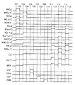
- FIG. 12 corresponds to an example of a timing chart showing operations of the memory cell MC, the memory cell MCR shown in FIG. 10, and the circuits 530, 540 and the current source circuit 550 shown in FIG.
- an operation of storing the first analog data in the memory cell MC and the memory cell MCR is performed at time T01 to time T04.
- an operation of setting the offset current Ioffset flowing to the circuits 530 and 540 is performed.
- an operation of acquiring data corresponding to the product-sum value of the first analog data and the second analog data is performed.
- a low level potential is supplied to the wiring VR [q] and the wiring VR [q + 1]. Further, all the wirings having a predetermined potential connected to the circuit 530 are supplied with a high level potential VDD. In addition, all the wirings having a predetermined potential connected to the circuit 540 are supplied with a low level potential VSS. Further, all the wirings having a predetermined potential connected to the current source circuit 550 are supplied with a high level potential VDD.
- Tr11, Tr21, Tr24, Tr27 [q], Tr27 [q + 1], and Tr28 operate in the saturation region.
- a high level potential is applied to the wiring WW [p]
- a low level potential is applied to the wiring WW [p + 1].
- the transistor Tr12 is turned on in the memory cell MC [p, q], the memory cell MC [p, q + 1], and the memory cell MCR [p] shown in FIG.
- the transistor Tr12 remains off in the memory cell MC [p + 1, q], the memory cell MC [p + 1, q + 1], and the memory cell MCR [p + 1].
- a potential obtained by subtracting the first analog potential from the first reference potential VPR is applied to the wiring WD [q] and the wiring WD [q + 1] shown in FIG.
- the potential VPR-Vx [p, q] is applied to the wiring WD [q]
- the potential VPR-Vx [p, q + 1] is applied to the wiring WD [q + 1].
- the first reference potential VPR is applied to the wiring WDREF
- a potential between the potential VSS and the potential VDD for example, the potential (VDD + VSS) / 2 is applied to the wiring RW [p] and the wiring RW [p + 1] as a reference potential.
- potential VPR-Vx [p, q] is applied to node N [p, q] of memory cell MC [p, q] shown in FIG. 10 through transistor Tr12, and memory cell MC [p, q + 1].
- the potential VPR-Vx [p, q + 1] is given to the node N [p, q + 1] of the memory cell via the transistor Tr12, and the node NREF [p] of the memory cell MCR [p] is given the first potential via the transistor Tr12. Reference potential VPR is applied.
- the potential applied to the wiring WW [p] shown in FIG. 10 changes from high level to low level, and the memory cell MC [p, q], the memory cell MC [p, q + 1], the memory cell MCR
- the transistor Tr12 is turned off at [p].
- the potential VPR-Vx [p, q] is held at the node N [p, q] and the potential VPR-Vx [p, q + 1] is held at the node N [p, q + 1].
- the first reference position VPR is held in [p].
- the potential of the wiring WW [p] illustrated in FIG. 10 is maintained at low level, and a high level potential is applied to the wiring WW [p + 1].
- the transistor Tr12 is turned on in the memory cell MC [p + 1, q], the memory cell MC [p + 1, q + 1], and the memory cell MCR [p + 1] shown in FIG.
- the transistor Tr12 maintains the off state.
- a potential obtained by subtracting the first analog potential from the first reference potential VPR is applied to the wiring WD [q] and the wiring WD [q + 1] shown in FIG.
- the potential VPR-Vx [p + 1, q] is applied to the wiring WD [q]
- the potential VPR-Vx [p + 1, q + 1] is applied to the wiring WD [q + 1].
- the first reference potential VPR is applied to the wiring WDREF
- a potential between the potential VSS and the potential VDD for example, the potential (VDD + VSS) / 2 is applied to the wiring RW [p] and the wiring RW [p + 1] as a reference potential.
- potential VPR-Vx [p + 1, q] is applied to node N [p + 1, q] of memory cell MC [p + 1, q] shown in FIG. 10 via transistor Tr12, and memory cell MC [p + 1, q + 1].
- the potential VPR-Vx [p + 1, q + 1] is applied to the node N [p + 1, q + 1] of the memory cell via the transistor Tr12, and the node NREF [p + 1] of the memory cell MCR [p + 1] is Reference potential VPR is applied.
- the potential applied to wiring WW [p + 1] shown in FIG. 10 changes from high level to low level, and memory cell MC [p + 1, q], memory cell MC [p + 1, q + 1], memory cell MCR.
- the transistor Tr12 is turned off at [p + 1].
- the potential VPR-Vx [p + 1, q] is held at the node N [p + 1, q]
- the potential VPR-Vx [p + 1, q + 1] is held at the node N [p + 1, q + 1].
- the first reference potential VPR is held at [p + 1].
- a high-level potential is applied to the wiring ORP and the wiring ORM illustrated in FIG.
- a high level potential is applied to the wiring ORM to turn on the transistor Tr26, and the gate of the transistor Tr24 is reset by applying the potential VDD. Be done.
- a high level potential is applied to the wiring ORP, so that the transistor Tr23 is turned on and the potential VSS is applied to the gate of the transistor Tr21. It is reset by.
- the potential applied to the wiring ORP and the wiring ORM illustrated in FIG. 10 changes from high level to low level, and the transistor Tr26 is turned off in the circuit 530 [q] and the circuit 530 [q + 1], and the circuit 540 The transistor Tr23 is turned off in [q] and the circuit 540 [q + 1].
- the potential VDD is held at the gate of the transistor Tr24 in the circuits 530 [q] and 530 [q + 1]
- the potential VSS is held at the gate of the transistor Tr21 in the circuits 540 [q] and 540 [q + 1]. .
- a high level potential is applied to the wiring OSP illustrated in FIG. Further, a potential between the potential VSS and the potential VDD, for example, a potential (VDD + VSS) / 2, is applied to the wiring RW [p] and the wiring RW [p + 1] illustrated in FIG. 10 as a reference potential.
- a potential between the potential VSS and the potential VDD for example, a potential (VDD + VSS) / 2
- VDD + VSS VDD + VSS
- the transistor Tr11 of the memory cell MC [p, q] shown in FIG. Means that the sum of the current which can be drawn and the current which can be drawn in the transistor Tr11 of the memory cell MC [p + 1, q] is smaller than the drain current of the transistor Tr27 [q]. Therefore, when the current ⁇ I [q] is positive, when the transistor Tr22 is turned on in the circuit 540 [q], part of the drain current of the transistor Tr27 [q] flows into the gate of the transistor Tr21, and the potential of the gate rises Begin to.
- the potential of the gate of the transistor Tr21 converges to a predetermined value.
- the potential applied to the wiring OSP illustrated in FIG. 11 changes from high level to low level, and the transistor Tr22 is turned off in the circuits 540 [q] and 540 [q + 1].
- the potential of the gate of the transistor Tr21 is held.
- the circuit 540 [q] maintains the state set to the current source capable of flowing the current ICP [q]
- the circuit 540 [q + 1] maintains the state set to the current source capable of flowing the current ICP [q + 1].
- a high level potential is applied to the wiring OSM illustrated in FIG. Further, a potential between the potential VSS and the potential VDD, for example, a potential (VDD + VSS) / 2, is applied to the wiring RW [p] and the wiring RW [p + 1] illustrated in FIG. 10 as a reference potential.
- a potential between the potential VSS and the potential VDD for example, a potential (VDD + VSS) / 2
- VDD + VSS VDD + VSS
- the transistor Tr11 of the memory cell MC [p, q] shown in FIG. Means that the sum of the current that can be drawn and the current that can be drawn by the transistor Tr11 of the memory cell MC [p + 1, q] is larger than the drain current of the transistor Tr27 [q]. Therefore, when the current ⁇ I [q] is negative, when the transistor Tr25 is turned on in the circuit 530 [q], the current flows from the gate of the transistor Tr24 to the wiring BL [q], and the potential of the gate starts to decrease.
- the potential of the gate of the transistor Tr24 converges to a predetermined value.
- the potential applied to the wiring OSM illustrated in FIG. 11 changes from high level to low level, and the transistor Tr25 is turned off in the circuit 530 [q] and the circuit 530 [q + 1].
- the potential of the gate of the transistor Tr24 is held. Therefore, the circuit 530 [q] maintains the state set to the current source capable of flowing the current ICM [q], and the circuit 530 [q + 1] maintains the state set to the current source capable of flowing the current ICM [q + 1].
- the transistor Tr21 has a function of drawing a current. Therefore, when the current I [q] flowing through the wiring BL [q] is larger than the current IREF flowing through the wiring BLREF at times T07 to T08, or the current flowing through the wiring BL [q + 1] is negative.
- the circuit 540 [q] or the circuit 540 [q + 1] has no excess or deficiency in the wiring BL [q] or the wiring BL [q + 1] It may be difficult to supply current to In this case, the transistor Tr11 of the memory cell MC and the circuit 540 [q] or the circuit 540 [q + 1] are used to balance the current flowing through the wiring BL [q] or the wiring BL [q + 1] and the current flowing through the wiring BLREF. It may be difficult for both the transistor Tr21 and the transistor Tr27 [q] or Tr27 [q + 1] to operate in the saturation region.
- the transistor Tr11, Tr21, Tr27 [q] or Tr27 [q + 1] operates at time T05 to time T06 to ensure operation in the saturation region.
- the potential of the gate of the transistor Tr24 may be set to such a height that a predetermined drain current can be obtained.
- the second analog potential Vw [p] is applied to the wiring RW [p] illustrated in FIG.
- a potential between the potential VSS and the potential VDD for example, a potential (VDD + VSS) / 2
- VDD + VSS potential (VDD + VSS) / 2
- Vw [p] the potential of the wiring RW [p] is the second analog potential Vw [p].
- the product-sum value of the first analog data and the second analog data corresponding to the memory cell MC [p, q] is obtained by subtracting the current Ioffset [q] from the current ⁇ I [q] from the equation 6 above. It can be seen that the current, ie, the current Iout [q] flowing out from the wiring BL [q] is reflected. Further, the product-sum value of the first analog data and the second analog data corresponding to memory cell MC [p, q + 1] is a current obtained by subtracting current Ioffset [q + 1] from current ⁇ I [q + 1], that is, wiring BL It can be seen that the current Iout [q + 1] flowing out of [q + 1] is reflected.
- the second analog potential Vw [p + 1] is applied to the wiring RW [p + 1] illustrated in FIG.
- a potential between the potential VSS and the potential VDD for example, the potential (VDD + VSS) / 2 is kept applied to the wiring RW [p] as the reference potential.
- the potential of the wiring RW [p + 1] is higher than the potential between the potential VSS which is the reference potential and the potential VDD, for example, the potential (VDD + VSS) / 2 by the potential difference Vw [p + 1].
- the potential of the wiring RW [p + 1] is the second analog potential Vw [p + 1].
- the product-sum value of the first analog data and the second analog data corresponding to the memory cell MC [p + 1, q] is obtained by subtracting the current Ioffset [q] from the current ⁇ I [q] from Equation 6 above. It can be seen that the current, that is, the current Iout [q] is reflected. Further, the product-sum value of the first analog data and the second analog data corresponding to memory cell MC [p + 1, q + 1] is a current obtained by subtracting current Ioffset [q + 1] from current ⁇ I [q + 1], that is, current Iout. It can be seen that [q + 1] is reflected.
- the second analog potential Vw [p] is applied to the wiring RW [p] illustrated in FIG. 10, and the second analog potential Vw [p + 1] is applied to the wiring RW [p + 1].
- the potential of the wiring RW [p] is higher than the potential between the potential VSS which is the reference potential and the potential VDD, for example, the potential (VDD + VSS) / 2 by a potential difference Vw [p].
- the potential of p + 1] is higher than the potential between the potential VSS which is the reference potential and the potential VDD, for example, the potential (VDD + VSS) / 2 by the potential difference Vw [p + 1]. It is assumed that the potential of the wiring RW [p] is the second analog potential Vw [p] and the potential of the wiring RW [p + 1] is the second analog potential Vw [p + 1].
- the amount of change in the potential of the first electrode of capacitive element C11 is substantially reflected in the amount of change in the potential of node N when interconnection RW [p + 1] attains second analog potential Vw [p + 1].
- the potential of the node N [p + 1, q] in the memory cell MC [p + 1, q] shown in FIG. 10 is VPR-Vx [p + 1, q] + Vw [p + 1], and the node N [in the memory cell MC [p + 1, q + 1]
- the potential of p + 1, q + 1] is VPR-Vx [p + 1, q + 1] + Vw [p + 1].
- the product-sum value of the first analog data and the second analog data corresponding to the memory cell MC [p, q] and the memory cell MC [p + 1, q] is the current ⁇ I [q ] Is subtracted from the current Ioffset [q], that is, reflected in the current Iout [q].
- the product-sum value of the first analog data and the second analog data corresponding to the memory cell MC [p, q + 1] and the memory cell MC [p + 1, q + 1] is the current ⁇ I [q + 1] to the current Ioffset [q + 1]. It can be seen that the current obtained by subtracting] is reflected in the current Iout [q + 1].
- the product-sum operation can be performed with a small circuit scale. Further, with the above configuration, product-sum operations can be performed at high speed. Further, with the above configuration, product-sum operations can be performed with low power consumption.
- a transistor with extremely low off-state current is preferably used as the transistor Tr12, Tr22, Tr23, Tr25, or Tr26.
- the transistor Tr12 By using a transistor with extremely low off-state current as the transistor Tr12, the potential of the node N can be held for a long time. Further, by using a transistor with extremely low off-state current as the transistors Tr22 and Tr23, the potential of the gate of the transistor Tr21 can be held for a long time. Further, by using a transistor with extremely low off-state current as the transistors Tr25 and Tr26, the potential of the gate of the transistor Tr24 can be held for a long time.
- An OS transistor may be used as a transistor with extremely low off-state current.
- the off-state current of the OS transistor normalized by the channel width can be 10 ⁇ 10 -21 A / ⁇ m (10 zept A / ⁇ m) or less at a source-drain voltage of 10 V and room temperature (about 25 ° C) It is.
- Embodiment 4 In this embodiment, a structural example of an OS transistor which can be used in the above embodiment will be described.
- FIG. 13A is a top view illustrating a configuration example of a transistor.
- 13B is a cross-sectional view taken along line X1-X2 of FIG. 13A
- FIG. 13C is a cross-sectional view taken along line Y1-Y2.
- the direction of the X1-X2 line may be referred to as a channel length direction
- the direction of the Y1-Y2 line may be referred to as a channel width direction.
- FIG. 13B is a view showing a cross-sectional structure in the channel length direction of the transistor
- FIG. 13C is a view showing a cross-sectional structure in the channel width direction of the transistor. Note that some components are omitted in FIG. 13A in order to clarify the device structure.
- the semiconductor device includes insulating layers 812 to 820, metal oxide films 821 to 824, and conductive layers 850 to 853.
- the transistor 801 is formed on the insulating surface.
- FIG. 13 illustrates the case where the transistor 801 is formed over the insulating layer 811.
- the transistor 801 is covered with an insulating layer 818 and an insulating layer 819.
- the insulating layer, the metal oxide film, the conductive layer, and the like included in the transistor 801 may be a single layer or a stack of a plurality of films.
- Various film forming methods such as sputtering method, molecular beam epitaxy method (MBE method), pulse laser ablation method (PLA method), CVD method, atomic layer deposition method (ALD method), etc. can be used for these fabrications.
- the CVD method includes a plasma CVD method, a thermal CVD method, an organic metal CVD method and the like.
- the conductive layer 850 includes a region functioning as a gate electrode of the transistor 801.
- the conductive layer 850 may be formed by stacking a conductive layer 850 a and a conductive layer 850 b made of different materials.
- the conductive layer 851 and the conductive layer 852 each include a region functioning as a source electrode or a drain electrode.
- the conductive layer 853 has a region functioning as a back gate electrode.
- the conductive layer 853 may be formed by stacking a conductive layer 853a and a conductive layer 853b made of different materials.
- the insulating layer 817 has a region functioning as a gate insulating layer on the gate electrode (front gate electrode) side, and the insulating layer formed by stacking the insulating layers 814 to 816 is a gate insulating layer on the back gate electrode side Have an area that functions as The insulating layer 818 functions as an interlayer insulating layer.
- the insulating layer 819 functions as a barrier layer.
- the metal oxide films 821 to 824 are collectively referred to as an oxide layer 830.
- the oxide layer 830 has a region in which a metal oxide film 821, a metal oxide film 822, and a metal oxide film 824 are sequentially stacked.
- the pair of metal oxide films 823 are located over the conductive layer 851 and the conductive layer 852, respectively.
- a channel formation region is mainly formed in the metal oxide film 822 in the oxide layer 830.
- the metal oxide film 824 covers the metal oxide films 821 to 823, the conductive layer 851, and the conductive layer 852.
- the insulating layer 817 is located between the metal oxide film 823 and the conductive layer 850.
- the conductive layer 851 and the conductive layer 852 each have a region overlapping with the conductive layer 850 with the metal oxide film 823, the metal oxide film 824, and the insulating layer 817 interposed therebetween.
- the conductive layer 851 and the conductive layer 852 are manufactured from a hard mask for forming the metal oxide film 821 and the metal oxide film 822. Therefore, the conductive layer 851 and the conductive layer 852 do not have a region in contact with the side surfaces of the metal oxide film 821 and the metal oxide film 822.
- the metal oxide films 821 and 822, the conductive layer 851, and the conductive layer 852 can be manufactured.
- a conductive film is formed over the two stacked metal oxide films.
- the conductive film is processed (etched) into a desired shape to form a hard mask.
- the shape of the two-layer metal oxide film is processed using a hard mask to form a stacked metal oxide film 821 and a metal oxide film 822.
- the hard mask is processed into a desired shape to form a conductive layer 851 and a conductive layer 852.
- insulating material used for the insulating layers 811 to 818 aluminum nitride, aluminum oxide, aluminum nitride oxide, aluminum oxynitride, magnesium oxide, silicon oxide, silicon oxide, silicon nitride oxide, silicon oxynitride, gallium oxynitride, germanium oxide, There are yttrium oxide, zirconium oxide, lanthanum oxide, neodymium oxide, hafnium oxide, tantalum oxide, aluminum silicate and the like.
- the insulating layers 811 to 818 are formed of a single layer or a stack of these insulating materials.
- the layers constituting the insulating layers 811 to 818 may contain a plurality of insulating materials.
- oxynitride refers to a compound in which the content of oxygen is higher than nitrogen
- nitrided oxide refers to a compound in which the content of nitrogen is higher than oxygen
- the insulating layers 816 to 818 are preferably insulating layers containing oxygen.
- the insulating layers 816 to 818 are more preferably formed using an insulating film from which oxygen is released by heating (hereinafter, also referred to as “an insulating film containing excess oxygen”).
- an insulating film containing excess oxygen By supplying oxygen to the oxide layer 830 from the insulating film containing excess oxygen, oxygen vacancies in the oxide layer 830 can be compensated. As a result, the reliability and electrical characteristics of the transistor 801 can be improved.
- the insulating layer containing excess oxygen refers to an oxygen molecule having a surface temperature of 100 ° C. to 700 ° C., or 100 ° C. to 500 ° C., in TDS (Thermal Desorption Spectroscopy).
- the film has a release amount of 1.0 ⁇ 10 18 molecules / cm 3 or more. More preferably, the release amount of oxygen molecules is 3.0 ⁇ 10 20 molecules / cm 3 or more.
- the insulating film containing excess oxygen can be formed by performing treatment for adding oxygen to the insulating film.
- the treatment for adding oxygen can be performed by heat treatment in an oxygen atmosphere, ion implantation, ion doping, plasma immersion ion implantation, plasma treatment, or the like.
- oxygen gas such as 16 O 2 or 18 O 2 , nitrous oxide gas or ozone gas can be used.
- the hydrogen concentration in the insulating layers 812 to 819 is preferably reduced.
- the hydrogen concentration is 2 ⁇ 10 20 atoms / cm 3 or less, preferably 5 ⁇ 10 19 atoms / cm 3 or less, more preferably 1 ⁇ 10 19 atoms / cm 3 or less, and 5 ⁇ 10 18 atoms / cm 3 or less is more preferable.
- the above-mentioned hydrogen concentration is a value measured by secondary ion mass spectrometry (SIMS).
- the transistor 801 preferably has a structure in which the oxide layer 830 is surrounded by an insulating layer having a barrier property to oxygen and hydrogen (hereinafter also referred to as a barrier layer). With such a structure, release of oxygen from the oxide layer 830 and entry of hydrogen into the oxide layer 830 can be suppressed. As a result, the reliability and electrical characteristics of the transistor 801 can be improved.
- the insulating layer 819 may function as a barrier layer, and at least one of the insulating layers 811 812 814 may function as a barrier layer.
- the barrier layer can be formed of a material such as aluminum oxide, aluminum oxynitride, gallium oxide, gallium oxynitride, yttrium oxide, yttrium oxynitride, hafnium oxide, hafnium oxynitride, or silicon nitride.
- the insulating layers 811 to 819 function as barrier layers, respectively.
- the insulating layers 816 to 818 are oxide layers containing excess oxygen.
- the insulating layer 811 is silicon nitride
- the insulating layer 812 is aluminum oxide
- the insulating layer 813 is silicon oxynitride.
- the insulating layers 814 to 816 having a function as a gate insulating layer on the back gate electrode side are stacked layers of silicon oxide, aluminum oxide, and silicon oxide.
- the insulating layer 817 having a function as a gate insulating layer on the front gate side is silicon oxynitride.
- the insulating layer 818 having a function as an interlayer insulating layer is silicon oxide.
- the insulating layer 819 is aluminum oxide.
- Conductive materials used for the conductive layers 850 to 853 include metals such as molybdenum, titanium, tantalum, tungsten, aluminum, copper, chromium, neodymium, and scandium, or metal nitrides containing the above-described metals (tantalum nitride, There are titanium nitride, molybdenum nitride, tungsten nitride) and the like.
- a conductive material such as tin oxide can be used.
- the conductive layer 850 is a tantalum nitride or tungsten single layer.
- conductive layer 850 is a stack of tantalum nitride, tantalum and tantalum nitride.
- the conductive layer 851 is a single layer of tantalum nitride or a stack of tantalum nitride and tungsten.
- the configuration of the conductive layer 852 is the same as that of the conductive layer 851.
- the conductive layer 853 is a single layer of tantalum nitride or a stack of tantalum nitride and tungsten.
- the metal oxide film 822 preferably has a large energy gap.
- the energy gap of the metal oxide film 822 is 2.5 eV or more and 4.2 eV or less, preferably 2.8 eV or more and 3.8 eV or less, and more preferably 3 eV or more and 3.5 eV or less.
- the oxide layer 830 preferably has crystallinity. At least the metal oxide film 822 preferably has crystallinity. With the above structure, the transistor 801 with high reliability and good electrical characteristics can be realized.
- An oxide applicable to the metal oxide film 822 is, for example, an In—Ga oxide, an In—Zn oxide, or an In—M—Zn oxide (M is Al, Ga, Y, or Sn).
- the metal oxide film 822 is not limited to the oxide layer containing indium.
- the metal oxide film 822 can be formed of, for example, a Zn-Sn oxide, a Ga-Sn oxide, a Zn-Mg oxide, or the like.
- the metal oxide films 821, 823, and 824 can also be formed using the same oxide as the metal oxide film 822. In particular, the metal oxide films 821, 823 and 824 can be formed of Ga oxide, respectively.
- the metal oxide film 821 preferably contains at least one of the metal elements constituting the metal oxide film 822 as a component. Thus, interface states are less likely to be formed at the interface between the metal oxide film 822 and the metal oxide film 821, and variations in electrical characteristics such as threshold voltage of the transistor 801 can be reduced.
- the metal oxide film 824 preferably contains at least one of the metal elements constituting the metal oxide film 822 as a component. Thus, interface scattering is less likely to occur at the interface between the metal oxide film 822 and the metal oxide film 824, and movement of carriers is less likely to be inhibited; therefore, the field-effect mobility of the transistor 801 can be increased.
- the carrier mobility of the metal oxide film 822 is preferably the highest.
- a channel can be formed in the metal oxide film 822 provided away from the insulating layers 816 and 817.
- an In-containing metal oxide such as an In-M-Zn oxide can increase carrier mobility by increasing the In content.
- An oxide with a high indium content has higher mobility than an oxide with a low indium content. Therefore, carrier mobility can be increased by using an oxide with a high content of indium for the metal oxide film.
- the metal oxide film 822 is formed of In—Ga—Zn oxide
- the metal oxide films 821 and 823 are formed of Ga oxide.
- the In content ratio corresponds to the In content ratio of the metal oxide film 822, and the In content of the metal oxide films 821 and 823. Make it higher than the rate.
- the In content can be changed by changing the atomic ratio of the metal element of the target.
- the atomic ratio In: M: Zn of the metal element of the target used for forming the metal oxide film 822 is preferably 1: 1: 1, 3: 1: 2, or 4: 2: 4.1.
- the atomic ratio In: M: Zn of the metal element of the target used for forming the metal oxide films 821 and 823 is preferably 1: 3: 2 or 1: 3: 4.
- the impurity concentration of the oxide layer 830 is preferably reduced.
- hydrogen, nitrogen, carbon, silicon, and metal elements other than main components are impurities.
- hydrogen and nitrogen contribute to the formation of donor levels and increase the carrier density.
- silicon and carbon contribute to the formation of impurity levels in the metal oxide. The impurity levels become traps and may degrade the electrical characteristics of the transistor.
- the oxide layer 830 has a region in which the silicon concentration is 2 ⁇ 10 18 atoms / cm 3 or less, preferably 2 ⁇ 10 17 atoms / cm 3 or less.
- the carbon concentration of the oxide layer 830 is similar.
- the oxide layer 830 has a region in which the alkali metal concentration is 1 ⁇ 10 18 atoms / cm 3 or less, preferably 2 ⁇ 10 16 atoms / cm 3 or less. The same applies to the concentration of the alkaline earth metal in the oxide layer 830.
- the oxide layer 830 has a hydrogen concentration of less than 1 ⁇ 10 20 atoms / cm 3 , preferably less than 1 ⁇ 10 19 atoms / cm 3 , more preferably less than 5 ⁇ 10 18 atoms / cm 3 , still more preferably It has a region of less than 1 ⁇ 10 18 atoms / cm 3 .
- the impurity concentration of the above-described oxide layer 830 is a value obtained by SIMS.
- the metal oxide film 822 When the metal oxide film 822 has an oxygen vacancy, hydrogen may enter a site of the oxygen vacancy to form a donor level. As a result, the on current of the transistor 801 is reduced. The site of oxygen deficiency is more stable when oxygen enters than hydrogen is entered. Therefore, by reducing oxygen vacancies in the metal oxide film 822, the on-state current of the transistor 801 can be increased in some cases. Therefore, reducing hydrogen in the metal oxide film 822 is effective for preventing the influx of hydrogen into the site of oxygen vacancies in on-current characteristics.
- Hydrogen contained in a metal oxide may form oxygen vacancies because it reacts with oxygen bonded to a metal atom to form water.
- the entry of hydrogen into an oxygen vacancy may generate electrons that are carriers.
- a part of hydrogen may be bonded to oxygen which is bonded to a metal atom to generate an electron which is a carrier. Since the metal oxide film 822 is provided with a channel formation region, the transistor 801 is likely to be normally on when the metal oxide film 822 contains hydrogen. Therefore, it is preferable that hydrogen in the metal oxide film 822 be reduced as much as possible.
- the metal oxide film 822 may have an n-type region 822 n in a region in contact with the conductive layer 851 or the conductive layer 852.
- oxygen in the metal oxide film 822 is extracted into the conductive layer 851 or the conductive layer 852, or a conductive material included in the conductive layer 851 or the conductive layer 852 is combined with an element in the metal oxide film 822. It is formed by phenomena such as By formation of the region 822 n, the contact resistance between the conductive layer 851 or the conductive layer 852 and the metal oxide film 822 can be reduced.
- FIG. 13 shows an example of the oxide layer 830 having a four-layer structure, it is not limited thereto.
- the oxide layer 830 can have a three-layer structure without the metal oxide film 821 or the metal oxide film 823.
- a metal oxide film similar to the metal oxide films 821 to 824 may be formed at any two or more places between the optional layer of the oxide layer 830, above the oxide layer 830, and below the oxide layer 830.
- a layer or layers can be provided.
- FIG. 14 is a schematic view of an energy band structure of a channel formation region of the transistor 801.
- Ec816e, Ec821e, Ec822e, Ec824e, and Ec817e indicate the energy of the lower end of the conduction band of the insulating layer 816, the metal oxide film 821, the metal oxide film 822, the metal oxide film 824, and the insulating layer 817, respectively. ing.
- the difference between the vacuum level and the energy at the lower end of the conduction band is obtained by subtracting the energy gap from the difference between the vacuum level and the energy at the upper end of the valence band (also referred to as ionization potential). It becomes a value.
- the energy gap can be measured using a spectroscopic ellipsometer (UT-300 manufactured by HORIBA JOBIN YVON).
- the energy difference between the vacuum level and the top of the valence band can be measured using an ultraviolet photoelectron spectroscopy (UPS) apparatus (VersaProbe, manufactured by PHI).
- Ec 816 e and E c 817 e are closer to a vacuum level (smaller in electron affinity) than E c 821 e, E c 822 e, and E c 824 e.
- the metal oxide film 822 has electron affinity higher than that of the metal oxide films 821 and 824.
- the difference in electron affinity between the metal oxide film 822 and the metal oxide film 821 and the difference in electron affinity between the metal oxide film 822 and the metal oxide film 824 are respectively 0.07 eV or more and 1.3 eV or less It is.
- the difference in electron affinity is preferably 0.1 eV or more and 0.7 eV or less, and more preferably 0.15 eV or more and 0.4 eV or less.
- the electron affinity is the difference between the vacuum level and the energy at the lower end of the conduction band.
- a channel is mainly included in the metal oxide film 822 having high electron affinity among the metal oxide film 821, the metal oxide film 822, and the metal oxide film 824. It is formed.
- Indium gallium oxide has a small electron affinity and a high oxygen blocking property. Therefore, it is preferable that the metal oxide film 824 contains indium gallium oxide.
- the gallium atom ratio [Ga / (In + Ga)] is, for example, 70% or more, preferably 80% or more, and more preferably 90% or more.
- a mixed region of the metal oxide film 821 and the metal oxide film 822 may be present between the metal oxide film 821 and the metal oxide film 822.
- a mixed region of the metal oxide film 824 and the metal oxide film 822 may exist between the metal oxide film 824 and the metal oxide film 822. Since the mixed region has a low interface state density, the stacked region of the metal oxide films 821, 822, and 824 has a band structure in which energy changes continuously in the vicinity of each interface (also referred to as continuous junction) It becomes.
- the difference between Ec821e and Ec822e, and the difference between Ec824e and Ec822e is set to 0.1 eV or more, respectively. More preferably, it is 0.15 eV or more.
- the transistor 801 can have a structure without a back gate electrode.
- FIG. 15 illustrates an example of a stacked structure of a semiconductor device 860 in which a transistor Tr100 which is a Si transistor, a transistor Tr200 which is an OS transistor, and a capacitive element C100 are stacked.
- the semiconductor device 860 is formed of a stack of a CMOS layer 871, wiring layers W 1 to W 5 , a transistor layer 872, and wiring layers W 6 and W 7 .
- a transistor Tr100 is provided in the CMOS layer 871.
- the channel formation region of the transistor Tr100 is provided in the single crystal silicon wafer 870.
- the gate electrode 873 of the transistor Tr100 via the wiring layer W 1 to W 5, and is connected to one electrode 875 of the capacitor C100.
- the transistor Tr 200 is provided in the transistor layer 872.
- the transistor Tr200 has the same structure as the transistor 801 (FIG. 13).
- An electrode 874 corresponding to one of the source and the drain of the transistor Tr200 is connected to one electrode 875 of the capacitive element C100.
- the transistor Tr200 is exemplified a case having a back gate electrode to the wiring layer W 5. Further, the wiring layer W 6 being the capacitor C100 is provided.
- the area of the circuit can be reduced.
- the transistor Tr100 can be used as the transistor Tr11 in FIG. 10
- the transistor Tr200 can be used as the transistor Tr12
- the capacitive element C100 can be used as the capacitive element C11.
- the transistor Tr100 can be used as the transistor Tr21 or Tr24 in FIG. 11
- the transistor Tr200 can be used as the transistor Tr22, Tr23, Tr25, or Tr26
- the capacitive element C100 can be used as the capacitive element C21 or C22.
- CAC-OS or CAC-metal oxide has a conductive function in part of the material and an insulating function in part of the material, and functions as a semiconductor in the whole of the material.
- the conductive function is a function of causing electrons (or holes) to be carriers
- the insulating function is a carrier. It is a function that does not flow electrons.
- a function of switching can be imparted to the CAC-OS or the CAC-metal oxide by causing the conductive function and the insulating function to be complementary to each other.
- CAC-OS or CAC-metal oxide has a conductive region and an insulating region.
- the conductive region has the above-mentioned conductive function
- the insulating region has the above-mentioned insulating function.
- the conductive region and the insulating region may be separated at the nanoparticle level.
- the conductive region and the insulating region may be unevenly distributed in the material.
- the conductive region may be observed as connected in a cloud shape with a blurred periphery.
- the conductive region and the insulating region are each dispersed in the material with a size of 0.5 nm or more and 10 nm or less, preferably 0.5 nm or more and 3 nm or less There is.
- CAC-OS or CAC-metal oxide is composed of components having different band gaps.
- CAC-OS or CAC-metal oxide is composed of a component having a wide gap resulting from the insulating region and a component having a narrow gap resulting from the conductive region.
- the carrier when the carrier flows, the carrier mainly flows in the component having the narrow gap.
- the component having the narrow gap acts complementarily to the component having the wide gap, and the carrier also flows to the component having the wide gap in conjunction with the component having the narrow gap. Therefore, when the above-described CAC-OS or CAC-metal oxide is used for a channel formation region of a transistor, high current driving force, that is, high on current, and high field effect mobility can be obtained in the on state of the transistor.
- CAC-OS or CAC-metal oxide can also be called a matrix composite (matrix composite) or a metal matrix composite (metal matrix composite).
- the CAC-OS is one configuration of a material in which, for example, an element constituting a metal oxide is 0.5 nm or more and 10 nm or less, preferably 1 nm or more and 2 nm or less, or a size in the vicinity thereof. Note that in the following, in the metal oxide, one or more metal elements are unevenly distributed, and the region having the metal element has a size of 0.5 nm or more and 10 nm or less, preferably 1 nm or more and 2 nm or less, or the size thereof
- the state of mixing in is also called mosaic or patch.
- the metal oxide preferably contains at least indium.
- One or more selected from the above may be included.
- CAC-OS in the In-Ga-Zn oxide is an indium oxide (hereinafter referred to as InO).
- InO indium oxide
- X1 X1 is a real number greater than 0
- indium zinc oxide hereinafter, In X2 Zn Y2 O Z2 (X2, Y2, and Z2 are real numbers greater than 0)
- GaO X3 X3 is a real number greater than 0)
- Ga X4 Zn Y4 O Z4 X4, Y4, and Z4 are real numbers greater than 0) to.
- the material becomes mosaic by separate into, mosaic InO X1 or in X2 Zn Y2 O Z2, is a configuration in which uniformly distributed in the film (hereinafter Also referred to as a cloud-like.)
- CAC-OS is a composite metal oxide having a structure in which a region in which GaO X3 is a main component and a region in which In X2 Zn Y2 O Z2 or InO X1 is a main component are mixed.
- the ratio of the atomic ratio of In to the element M in the first region is larger than the atomic ratio of In to the element M in the second region, It is assumed that the concentration of In is higher than that in the region 2.
- IGZO is a common name and may refer to one compound of In, Ga, Zn, and O. Representative examples are represented by InGaO 3 (ZnO) m1 (m1 is a natural number), or In (1 + x0) Ga ( 1-x0) O 3 (ZnO) m0 (-1 ⁇ x0 ⁇ 1, m0 is an arbitrary number) Crystalline compounds are mentioned.
- the crystalline compound has a single crystal structure, a polycrystalline structure, or a c-axis aligned crystal (CAAC) structure.
- CAAC c-axis aligned crystal
- the CAAC structure is a crystal structure in which a plurality of IGZO nanocrystals have c-axis orientation and are connected without orientation in the a-b plane.
- CAC-OS relates to the material composition of metal oxides.
- the CAC-OS refers to a region observed in the form of nanoparticles mainly composed of Ga in a material configuration including In, Ga, Zn, and O, and nanoparticles composed mainly of In in some components.
- region observed in shape says the structure currently disperse
- CAC-OS does not include a stacked structure of two or more types of films different in composition. For example, a structure including two layers of a film containing In as a main component and a film containing Ga as a main component is not included.
- the CAC-OS may be a region observed in the form of nanoparticles mainly composed of the metal element, and a nano mainly composed of In as a main component.
- region observed in particle form says the structure currently each disperse
- the CAC-OS can be formed, for example, by sputtering under the condition that the substrate is not heated.
- one or more selected from an inert gas (typically, argon), an oxygen gas, and a nitrogen gas may be used as a deposition gas.
- an inert gas typically, argon
- oxygen gas typically, oxygen gas
- a nitrogen gas may be used as a deposition gas.
- the flow rate ratio of the oxygen gas to the total flow rate of the film forming gas at the time of film formation is preferably as low as possible.
- the flow rate ratio of the oxygen gas is preferably 0% to less than 30%, .
- CAC-OS has a feature that a clear peak is not observed when it is measured using a ⁇ / 2 ⁇ scan by the Out-of-plane method, which is one of X-ray diffraction (XRD) measurement methods. Have. That is, it can be understood from X-ray diffraction that the orientation in the a-b plane direction and the c-axis direction of the measurement region is not seen.
- XRD X-ray diffraction
- the CAC-OS has a ring-like high luminance region and a plurality of bright spots in the ring region. A point is observed. Therefore, it can be seen from the electron diffraction pattern that the crystal structure of the CAC-OS has an nc (nano-crystal) structure having no orientation in the planar direction and in the cross-sectional direction.
- a region in which GaO X3 is a main component by EDX mapping acquired using energy dispersive X-ray spectroscopy (EDX: Energy Dispersive X-ray spectroscopy) It can be confirmed that the light emitting element and the region containing In X 2 Zn Y 2 O Z 2 or InO X 1 as the main components have a structure in which the elements are localized and mixed.
- the CAC-OS has a structure different from the IGZO compound in which the metal element is uniformly distributed, and has different properties from the IGZO compound. That is, CAC-OS is phase-separated into a region in which GaO X3 or the like is a main component and a region in which In X2 Zn Y2 O Z2 or InO X1 is a main component, and a region in which each element is a main component Has a mosaic-like structure.
- the region whose main component is In X2 Zn Y2 O Z2 or InO X1 is a region whose conductivity is higher than the region whose main component is GaO X3 or the like. That is, when carriers flow in a region mainly containing In X2 Zn Y2 O Z2 or InO X1 , conductivity as an oxide semiconductor is exhibited. Therefore, high field-effect mobility ( ⁇ ) can be realized by cloud-like distribution of a region containing In X 2 Zn Y 2 O Z 2 or InO X 1 as a main component in the oxide semiconductor.
- the region in which GaO X3 or the like is a main component is a region in which the insulating property is higher than the region in which In X2 Zn Y2 O Z2 or InO X1 is a main component.
- the region in which GaO X3 or the like is a main component is a region in which the insulating property is higher than the region in which In X2 Zn Y2 O Z2 or InO X1 is a main component.
- CAC-OS when CAC-OS is used for a semiconductor element, the insulating property caused by GaO X3 and the like and the conductivity caused by In X 2 Zn Y 2 O Z 2 or InO X 1 act complementarily to achieve high results. On current (I on ) and high field effect mobility ( ⁇ ) can be realized.
- CAC-OS is optimal for various semiconductor devices.
- 16A to 16F illustrate electronic devices. These electronic devices include a housing 5000, a display portion 5001, a speaker 5003, an LED lamp 5004, an operation key 5005 (including a power switch or an operation switch), a connection terminal 5006, a sensor 5007 (force, displacement, position, speed, Measuring acceleration, angular velocity, number of rotations, distance, light, liquid, magnetism, temperature, chemical, voice, time, hardness, electric field, current, voltage, power, radiation, flow rate, humidity, inclination, vibration, odor or infrared light Functions), a microphone 5008, and the like.
- a sensor 5007 force, displacement, position, speed, Measuring acceleration, angular velocity, number of rotations, distance, light, liquid, magnetism, temperature, chemical, voice, time, hardness, electric field, current, voltage, power, radiation, flow rate, humidity, inclination, vibration, odor or infrared light Functions
- a microphone 5008 and the like.
- FIG. 16A illustrates a mobile computer, which can include a switch 5009, an infrared port 5010, and the like in addition to the above components.
- FIG. 16B shows a portable image reproducing apparatus (for example, a DVD reproducing apparatus) provided with a recording medium, which may have a second display portion 5002, a recording medium reading portion 5011, and the like in addition to those described above. it can.
- FIG. 16C illustrates a goggle type display, which can include a second display portion 5002, a support portion 5012, an earphone 5013, and the like in addition to the above components.
- FIG. 16D illustrates a portable game machine, which can include the memory medium reading portion 5011 and the like in addition to the above components.
- FIG. 16E illustrates a digital camera having a television receiving function, which can include an antenna 5014, a shutter button 5015, an image receiving portion 5016, and the like in addition to the above components.
- FIG. 16F illustrates a portable game machine, which can include the second display portion 5002, the recording medium reading portion 5011, and the like in addition to the above components.
- the electronic devices illustrated in FIGS. 16A to 16F can have various functions. For example, a function of displaying various information (still image, moving image, text image, etc.) on the display unit, a touch panel function, a calendar, a function of displaying date or time, etc., a function of controlling processing by various software (programs), A wireless communication function, a function of connecting to various computer networks using the wireless communication function, a function of transmitting or receiving various data using the wireless communication function, reading out and displaying a program or data recorded in a recording medium It can have a function of displaying on a unit, and the like.
- the function of displaying image information mainly on one display unit and displaying character information mainly on another display unit or considering parallax in a plurality of display units It is possible to have a function of displaying a three-dimensional image and the like by displaying the captured image. Furthermore, in an electronic device having an image receiving unit, the function of capturing a still image, the function of capturing a moving image, the function of automatically or manually correcting the captured image, the captured image in a recording medium (externally or built in a camera) A function to save, a function to display a captured image on a display portion, and the like can be provided. Note that the electronic devices illustrated in FIGS. 16A to 16F can have various functions without limitation to the above.
- the electronic device described in this embodiment can include a battery and can perform the wireless power supply described in the above embodiment.
- 17A and 17B illustrate usage examples of the electronic device.
- FIG. 17A shows an example in which the information terminal is operated in the car of a mobile object such as a car.
- a handle 5103 has an antenna inside. Power can be supplied to the electronic device 5100 from an antenna in the handle 5103.
- the electronic device 5100 has a battery and is charged by wireless power feeding.
- a jig that can fix the electronic device 5100 may be provided on the handle 5103. If the electronic device 5100 is fixed to the handle 5103, hands-free phone calls or video phone calls can be made.
- voice authentication can be performed by the microphone provided in the electronic device 5100, and the vehicle can be steered by the voice of the driver.
- position information can be displayed on the display portion 5102 by operating the electronic device 5100 while the vehicle is stopped. Further, information not displayed on the display unit 5101 of the car, for example, the engine speed, the steering wheel angle, the temperature, the tire pressure, etc. may be displayed on the display unit 5102.
- the display portion 5102 has a touch input function.
- the state of the outside of the vehicle can be displayed on the display portion 5102 using one or more cameras for capturing the outside of the vehicle, and can also be used, for example, as a back monitor.
- information such as traveling speed is wirelessly received from the car, and while traveling while monitoring the traveling speed, the driver is photographed from the electronic device 5100, and the eyes are closed.
- the driver can appropriately select settings such as vibrating the electronic device 5100, a warning sound, and allowing music to flow.
- shooting of the driver may be stopped to save power, and the battery of the electronic device 5100 may be charged wirelessly while the vehicle is stopped.
- the electronic device 5100 be provided with many sensors and a plurality of antennas in order to have various functions.
- Mobiles such as cars have a power supply, but have limitations. Considering the power to drive the mobiles, it is preferable to reduce the power used for the electronic device 5100 as much as possible. The power consumption used by the device 5100 may shorten the travel distance. Even if the electronic device 5100 is provided with various functions, it is rare to use all the functions at the same time, and often only one function or two functions are used as needed.
- FIG. 17 (B) shows an example in which the information terminal is operated in an airplane or the like.
- the time during which an individual's information terminal can be used may be limited, and in the case of a long flight, it is desirable that an information terminal provided on the plane can be used.
- the electronic device 5200 includes a display unit 5202 that displays an image such as a movie, a game, or an advertisement, and is an information terminal capable of acquiring the current flight position, the remaining arrival time, and the like in real time by the communication function.
- the display portion 5202 has a touch input function.
- the electronic device 5200 is inserted into the concave portion provided in the sheet 5201 and the antenna installation portion 5203 is provided at a position overlapping with the electronic device 5200 so that wireless power feeding can be performed while being inserted.
- the electronic device 5200 can also function as a telephone or a communication tool when the user wishes to contact a crew member who is in poor physical condition or the like. If the electronic device 5200 is provided with a translation function or the like, communication can be made using the display portion 5202 of the electronic device 5200 even if the passenger is a passenger whose language is different. In addition, communication can be performed by using the display portion 5202 of the electronic device 5200 between crew members who are adjacent to each other and have different languages. In addition, for example, while the occupant is sleeping, the display unit 5202 can also be displayed in English as "Please do not wake up" or the like, and can also function as a message board.
- the electronic device 5200 may have a plurality of batteries for each function, and power saving can be achieved by turning on only the function to be used and turning off a function that is not in use. Further, among the plurality of batteries, the battery corresponding to the stopped function can be wirelessly supplied with power from the antenna installation unit 5203.
- the battery of the electronic device 5200 in each of the plurality of sheets may be designed to be used for emergency. Since all the electronic devices 5200 in each of the plurality of sheets are the same product and have the same design, the system may be configured to be connected in series as an emergency power supply.
- any one or more of lithium ion secondary batteries such as lithium polymer batteries, lithium ion capacitors, electric double layer capacitors, and redox capacitors can be used.
- FIG. 18 is a schematic cross-sectional view showing an example of a pacemaker.
- the pacemaker main body 5300 has at least batteries 5301a and 5301b, a regulator, a control circuit, an antenna 5304, a wire 5302 to the right atrium, and a wire 5303 to the right ventricle.
- the pacemaker body 5300 is placed in the body by surgery, and the two wires pass through the subclavian vein 5305 and the superior vena cava 5306 of the human body, and one wire tip is placed in the right ventricle and the other wire tip in the right atrium. To be done.
- the pacemaker main body 5300 has a plurality of batteries, it is highly safe and can function as an auxiliary power supply because one can function even if one breaks down. If the battery provided in the pacemaker is further divided into a plurality of thin batteries, it is mounted on a printed circuit board provided with a control circuit including a CPU and the like, and the pacemaker main body 5300 is miniaturized and the pacemaker main body 5300 is thick. Can be made thinner.
- an antenna that can transmit a physiological signal may be provided.
- physiological signals such as pulse, respiratory rate, heart rate, and temperature can be checked by an external monitor device. System for monitoring various cardiac activities.
- this pacemaker is also an example, and it may become various forms according to heart disease.
- the cochlear implant is one of the more popular artificial organs than pacemakers.
- a cochlear implant is a device that converts sound into an electrical signal and directly stimulates the auditory nerve with a stimulator placed in the cochlea.
- the cochlear implant is comprised of a first device to be implanted in the back of the ear during surgery and a second device to send sound to a first device which is picked up by a microphone and embedded.
- the first device and the second device are not electrically connected, but are systems that transmit and receive wirelessly.
- the first device comprises at least an antenna for receiving an electrical signal converted from sound and a wire reaching the cochlea.
- the second device at least includes an audio processing unit for converting sound into an electrical signal, and a transmission circuit for transmitting the electrical signal to the first device.
Landscapes
- Engineering & Computer Science (AREA)
- Computer Networks & Wireless Communication (AREA)
- Power Engineering (AREA)
- Signal Processing (AREA)
- Charge And Discharge Circuits For Batteries Or The Like (AREA)
Abstract
Description
本実施の形態では、図1乃至図5を用いて、本発明の一態様である給電装置および非接触給電システムについて説明する。また、本実施の形態では、本発明の一態様である給電装置および非接触給電システムについて、給電装置100および受電装置200を有する非接触給電システムを例に挙げて説明する。
第1のステップにおいて、最適な給電コイルの位置を決定する(図5(T1)参照)。上述のとおり、最適な給電コイル110の位置の決定は、検知装置130から送信された検知信号を制御装置120において処理することによって行うことができる。
第2のステップにおいて、給電コイル110が移動する(図5(T2)参照)。上述のとおり、移動装置140が、給電コイル110を移動させる機能を有する。
第3のステップにおいて、給電を開始する(図5(T3)参照)。上述のとおり、給電コイル110が、起電力を誘導する機能を有する。
第4のステップにおいて、受電コイル210が移動したかどうかを判別する(図5(T4)参照)。受電コイル210が、給電開始時の位置と異なる位置に移動したと判別した場合は、第5のステップに進み、受電コイル210が、給電開始時の位置から移動していないと判別した場合は、第6のステップに進む。
第5のステップにおいて、給電装置100は、給電を一時停止した後、第1のステップに進む(図5(T5)参照)。これによって、給電の途中に受電コイル210と、給電コイル110との位置関係がずれるようなことがあっても、無駄な電力を放出することを防ぐことができる。
第6のステップにおいて、交流電源111が、終了信号を受信した場合は、給電を終了し、交流電源111が、終了信号を受信しない場合は、第4のステップに進む(図5(T6)参照)。
本実施の形態では、上記実施の形態で説明した非接触給電システムに人工知能(AI:Artificial Intelligence)を用いた構成例について説明する。
図6に、制御装置120の構成例を示す。
次に、ニューラルネットワークNNのより具体的な構成例について説明する。ニューラルネットワークの構成例を図7に示す。ニューラルネットワークは、ニューロン回路NCと、ニューロン回路NC間に設けられたシナプス回路SCによって構成されている。
本実施の形態では、実施の形態2で説明したニューラルネットワークに用いることができる半導体装置の構成例について説明する。
半導体装置500の構成の一例を図8に示す。図8に示す半導体装置500は、記憶回路510(MEM)と、参照用記憶回路520(RMEM)と、回路530と、回路540と、を有する。半導体装置500は、さらに電流源回路550(CREF)を有していても良い。
=Σi{k(Vw[p]−Vth+VPR)2−k(Vw[p]−Vth+VPR−Vx[p、q])2}
=2kΣi(Vw[p]・Vx[p、q])−2kΣi(Vth−VPR)・Vx[p、q]−kΣiVx[p、q]2 (式4)
次いで、記憶回路510(MEM)と、参照用記憶回路520(RMEM)の具体的な構成の一例について、図9を用いて説明する。
次いで、回路530と、回路540と、電流源回路550(CREF)の具体的な構成の一例について、図11を用いて説明する。
次いで、図10乃至図12を用いて、本発明の一態様に係る半導体装置500の具体的な動作の一例について説明する。
本実施の形態では、上記実施の形態において用いることができるOSトランジスタの構成例について説明する。
図13(A)は、トランジスタの構成例を示す上面図である。図13(B)は、図13(A)のX1−X2線断面図であり、図13(C)はY1−Y2線断面図である。ここでは、X1−X2線の方向をチャネル長方向と、Y1−Y2線方向をチャネル幅方向と呼称する場合がある。図13(B)は、トランジスタのチャネル長方向の断面構造を示す図であり、図13(C)は、トランジスタのチャネル幅方向の断面構造を示す図である。なお、デバイス構造を明確にするため、図13(A)では、一部の構成要素が省略されている。
次に、OSトランジスタと他のトランジスタの積層によって構成される半導体装置の構造について説明する。
本実施の形態では、上記実施の形態で説明したOSトランジスタに用いることができる、金属酸化物について説明する。以下では特に、金属酸化物とCAC(Cloud−Aligned Composite)の詳細について説明する。
本実施の形態では、上記実施の形態で説明した受電装置を搭載することが可能な電子機器について説明する。
Claims (5)
- 給電コイルと、制御装置と、検知装置と、移動装置と、を有し、
前記給電コイルは、磁界を発生させる機能を有し、
前記制御装置は、前記給電コイルと、前記検知装置と、電気的に接続され、前記給電コイルの位置を決定する機能と、位置制御信号を送信する機能と、を有し、
前記移動装置は、前記位置制御信号を受信する機能と、前記位置制御信号に基づいて前記給電コイルを移動させる機能と、を有し、
前記検知装置は、第1の検知コイルと、第2の検知コイルと、を有し、
前記第1の検知コイルは、磁界を発生させる機能を有し、
前記第2の検知コイルは、磁束密度の変化を検知する機能を有する、給電装置。 - 給電コイルと、制御装置と、検知装置と、移動装置と、を有し、
前記給電コイルは、磁界を発生させる機能を有し、
前記制御装置は、前記給電コイルと、前記検知装置と、電気的に接続され、前記給電コイルの位置を決定する機能と、位置制御信号を送信する機能と、を有し、
前記移動装置は、前記位置制御信号を受信する機能と、前記位置制御信号に基づいて前記給電コイルを移動させる機能と、を有し、
前記検知装置は、第1のコイル群と、第2のコイル群とを有し、
前記第2のコイル群は、前記第1のコイル群の含むコイルのいずれか一に囲まれる領域に位置する、給電装置。 - 請求項2において、
前記第1のコイル群および前記第2のコイル群のすくなくともいずれか一方は、第1の検知コイルと、第2の検知コイルを含み、
前記第1の検知コイルは、磁界を発生させる機能を有し、
前記第2の検知コイルは、磁束密度の変化を検知する機能を有する、給電装置。 - 請求項1乃至3のいずれか一において、
前記制御装置は、ニューラルネットワークを有し、
前記ニューラルネットワークの入力層には、前記検知情報が入力され、
前記ニューラルネットワークの出力層から、前記制御信号が出力される給電装置。 - 請求項1乃至3のいずれか一に記載の給電装置と、受電装置と、を有し、
前記受電装置は、蓄電装置と、受電コイルと、を有し、
前記蓄電装置は、前記受電コイルに電気的に接続され、前記受電コイルに誘導される電力で充電される機能を有し、
前記制御装置は、前記受電コイルの位置に対応して前記電源コイルの位置を決定する機能を有する非接触給電システム。
Priority Applications (5)
| Application Number | Priority Date | Filing Date | Title |
|---|---|---|---|
| US16/629,052 US20200203995A1 (en) | 2017-07-14 | 2018-07-04 | Power-feeding device and wireless power-feeding system |
| DE112018003598.0T DE112018003598T5 (de) | 2017-07-14 | 2018-07-04 | Stromversorgungsvorrichtung und kontaktfreies Stromversorgungssystem |
| JP2019529319A JP7167023B2 (ja) | 2017-07-14 | 2018-07-04 | 給電装置および非接触給電システム |
| CN201880045594.4A CN110870163A (zh) | 2017-07-14 | 2018-07-04 | 供电装置及非接触供电系统 |
| KR1020207003993A KR20200029526A (ko) | 2017-07-14 | 2018-07-04 | 급전 장치 및 비접촉 급전 시스템 |
Applications Claiming Priority (2)
| Application Number | Priority Date | Filing Date | Title |
|---|---|---|---|
| JP2017-138238 | 2017-07-14 | ||
| JP2017138238 | 2017-07-14 |
Publications (1)
| Publication Number | Publication Date |
|---|---|
| WO2019012372A1 true WO2019012372A1 (ja) | 2019-01-17 |
Family
ID=65002500
Family Applications (1)
| Application Number | Title | Priority Date | Filing Date |
|---|---|---|---|
| PCT/IB2018/054931 Ceased WO2019012372A1 (ja) | 2017-07-14 | 2018-07-04 | 給電装置および非接触給電システム |
Country Status (6)
| Country | Link |
|---|---|
| US (1) | US20200203995A1 (ja) |
| JP (1) | JP7167023B2 (ja) |
| KR (1) | KR20200029526A (ja) |
| CN (1) | CN110870163A (ja) |
| DE (1) | DE112018003598T5 (ja) |
| WO (1) | WO2019012372A1 (ja) |
Cited By (7)
| Publication number | Priority date | Publication date | Assignee | Title |
|---|---|---|---|---|
| WO2021055898A1 (en) * | 2019-09-20 | 2021-03-25 | Energous Corporation | Systems and methods for machine learning based foreign object detection for wireless power transmission |
| US11381118B2 (en) | 2019-09-20 | 2022-07-05 | Energous Corporation | Systems and methods for machine learning based foreign object detection for wireless power transmission |
| KR20220106075A (ko) * | 2021-01-21 | 2022-07-28 | 후아웨이 디지털 파워 테크놀러지스 컴퍼니 리미티드 | 무선충전 장치, 자동 정렬 방식 및 충전 도크 |
| US11463179B2 (en) | 2019-02-06 | 2022-10-04 | Energous Corporation | Systems and methods of estimating optimal phases to use for individual antennas in an antenna array |
| JP2023527817A (ja) * | 2020-05-27 | 2023-06-30 | トヨタ自動車株式会社 | 無線車両電力転送およびずれ推定のためのシステムと方法 |
| WO2025115959A1 (ja) * | 2023-12-01 | 2025-06-05 | パナソニックIpマネジメント株式会社 | 制御方法及びプログラム |
| US12413097B2 (en) | 2021-12-29 | 2025-09-09 | Energous Corporation | Small form-factor devices with integrated and modular harvesting receivers, and shelving-mounted wireless-power transmitters for use therewith |
Families Citing this family (9)
| Publication number | Priority date | Publication date | Assignee | Title |
|---|---|---|---|---|
| DE102019110998A1 (de) * | 2019-04-29 | 2020-10-29 | Tdk Electronics Ag | Anordnungen eines Fahrzeug-Positionsbestimmungssystems, System, Verwendung und Verfahren |
| CN113555979B (zh) * | 2020-04-24 | 2025-02-11 | 北京小米移动软件有限公司 | 无线充电定位装置、方法及存储介质 |
| US11804737B2 (en) * | 2020-05-29 | 2023-10-31 | Renesas Electronics America Inc. | Universal wireless charging surface |
| US11610999B2 (en) * | 2020-06-10 | 2023-03-21 | Globalfoundries Dresden Module One Limited Liability Company & Co. Kg | Floating-gate devices in high voltage applications |
| CN113852219A (zh) * | 2020-06-28 | 2021-12-28 | 北京小米移动软件有限公司 | 无线充电系统和无线充电的实现方法 |
| WO2022034936A1 (ko) * | 2020-08-10 | 2022-02-17 | 엘지전자 주식회사 | 무선 전력 송신 장치 |
| WO2022155838A1 (zh) * | 2021-01-21 | 2022-07-28 | 华为数字能源技术有限公司 | 一种无线充电设备及无线充电底座 |
| CN113472088B (zh) * | 2021-07-09 | 2024-04-23 | 东集技术股份有限公司 | 一种无线充电方法及无线充电系统 |
| KR102576265B1 (ko) * | 2021-10-15 | 2023-09-07 | 단국대학교 산학협력단 | 무인 항공체의 자율 무선 배터리 충전 장치, 방법 및 프로그램 |
Citations (5)
| Publication number | Priority date | Publication date | Assignee | Title |
|---|---|---|---|---|
| JPH09215211A (ja) * | 1996-02-02 | 1997-08-15 | Sumitomo Wiring Syst Ltd | 電気自動車用充電システム |
| JP2009089464A (ja) * | 2007-09-27 | 2009-04-23 | Panasonic Corp | 電子機器および充電システム |
| WO2015177994A1 (ja) * | 2014-05-19 | 2015-11-26 | パナソニックIpマネジメント株式会社 | 携帯端末充電装置と、それを搭載した自動車 |
| WO2016088261A1 (ja) * | 2014-12-05 | 2016-06-09 | 三菱電機エンジニアリング株式会社 | 共振型電力伝送システム、送信装置及び給電位置制御システム |
| WO2017017959A1 (ja) * | 2015-07-29 | 2017-02-02 | パナソニックIpマネジメント株式会社 | ワイヤレス充電装置 |
Family Cites Families (11)
| Publication number | Priority date | Publication date | Assignee | Title |
|---|---|---|---|---|
| WO2009155030A2 (en) * | 2008-05-28 | 2009-12-23 | Georgia Tech Research Corporation | Systems and methods for providing wireless power to a portable unit |
| JP2010273472A (ja) | 2009-05-22 | 2010-12-02 | Canon Inc | 充電装置 |
| JP2010288431A (ja) * | 2009-06-15 | 2010-12-24 | Sanyo Electric Co Ltd | 電池内蔵機器と充電台 |
| DE102011077068A1 (de) * | 2011-06-07 | 2012-12-13 | Hilti Aktiengesellschaft | Verfahren und Vorrichtung zum Detektieren eines leitfähigen Objektes |
| JP5770556B2 (ja) * | 2011-07-29 | 2015-08-26 | 東光株式会社 | ワイヤレス電力伝送装置および相対位置検出方法 |
| JP2013118720A (ja) * | 2011-12-01 | 2013-06-13 | Sanyo Electric Co Ltd | 充電台 |
| JP5997554B2 (ja) | 2012-02-10 | 2016-09-28 | 東光株式会社 | ワイヤレス電力伝送装置 |
| US9410823B2 (en) * | 2012-07-13 | 2016-08-09 | Qualcomm Incorporated | Systems, methods, and apparatus for detection of metal objects in a predetermined space |
| DE102012020885A1 (de) * | 2012-10-24 | 2014-04-24 | Panasonic Corporation | Kontaktloses Leistungsversorgungssystem |
| JP6384991B2 (ja) * | 2013-10-28 | 2018-09-05 | パナソニック株式会社 | 送電装置及び無線電力伝送システム |
| US20170182903A1 (en) * | 2015-12-26 | 2017-06-29 | Intel Corporation | Technologies for wireless charging of electric vehicles |
-
2018
- 2018-07-04 WO PCT/IB2018/054931 patent/WO2019012372A1/ja not_active Ceased
- 2018-07-04 DE DE112018003598.0T patent/DE112018003598T5/de not_active Withdrawn
- 2018-07-04 CN CN201880045594.4A patent/CN110870163A/zh active Pending
- 2018-07-04 US US16/629,052 patent/US20200203995A1/en not_active Abandoned
- 2018-07-04 KR KR1020207003993A patent/KR20200029526A/ko not_active Ceased
- 2018-07-04 JP JP2019529319A patent/JP7167023B2/ja active Active
Patent Citations (5)
| Publication number | Priority date | Publication date | Assignee | Title |
|---|---|---|---|---|
| JPH09215211A (ja) * | 1996-02-02 | 1997-08-15 | Sumitomo Wiring Syst Ltd | 電気自動車用充電システム |
| JP2009089464A (ja) * | 2007-09-27 | 2009-04-23 | Panasonic Corp | 電子機器および充電システム |
| WO2015177994A1 (ja) * | 2014-05-19 | 2015-11-26 | パナソニックIpマネジメント株式会社 | 携帯端末充電装置と、それを搭載した自動車 |
| WO2016088261A1 (ja) * | 2014-12-05 | 2016-06-09 | 三菱電機エンジニアリング株式会社 | 共振型電力伝送システム、送信装置及び給電位置制御システム |
| WO2017017959A1 (ja) * | 2015-07-29 | 2017-02-02 | パナソニックIpマネジメント株式会社 | ワイヤレス充電装置 |
Cited By (12)
| Publication number | Priority date | Publication date | Assignee | Title |
|---|---|---|---|---|
| US11463179B2 (en) | 2019-02-06 | 2022-10-04 | Energous Corporation | Systems and methods of estimating optimal phases to use for individual antennas in an antenna array |
| US11784726B2 (en) | 2019-02-06 | 2023-10-10 | Energous Corporation | Systems and methods of estimating optimal phases to use for individual antennas in an antenna array |
| WO2021055898A1 (en) * | 2019-09-20 | 2021-03-25 | Energous Corporation | Systems and methods for machine learning based foreign object detection for wireless power transmission |
| US11381118B2 (en) | 2019-09-20 | 2022-07-05 | Energous Corporation | Systems and methods for machine learning based foreign object detection for wireless power transmission |
| US11831361B2 (en) | 2019-09-20 | 2023-11-28 | Energous Corporation | Systems and methods for machine learning based foreign object detection for wireless power transmission |
| US12418327B2 (en) | 2019-09-20 | 2025-09-16 | Energous Corporation | Systems and methods for machine learning zone-based foreign object detection for wireless power transmission |
| JP2023527817A (ja) * | 2020-05-27 | 2023-06-30 | トヨタ自動車株式会社 | 無線車両電力転送およびずれ推定のためのシステムと方法 |
| JP7719467B2 (ja) | 2020-05-27 | 2025-08-06 | トヨタ自動車株式会社 | 無線車両電力転送およびずれ推定のためのシステムと方法 |
| KR20220106075A (ko) * | 2021-01-21 | 2022-07-28 | 후아웨이 디지털 파워 테크놀러지스 컴퍼니 리미티드 | 무선충전 장치, 자동 정렬 방식 및 충전 도크 |
| KR102657710B1 (ko) * | 2021-01-21 | 2024-04-15 | 후아웨이 디지털 파워 테크놀러지스 컴퍼니 리미티드 | 무선충전 장치, 자동 정렬 방식 및 충전 도크 |
| US12413097B2 (en) | 2021-12-29 | 2025-09-09 | Energous Corporation | Small form-factor devices with integrated and modular harvesting receivers, and shelving-mounted wireless-power transmitters for use therewith |
| WO2025115959A1 (ja) * | 2023-12-01 | 2025-06-05 | パナソニックIpマネジメント株式会社 | 制御方法及びプログラム |
Also Published As
| Publication number | Publication date |
|---|---|
| CN110870163A (zh) | 2020-03-06 |
| KR20200029526A (ko) | 2020-03-18 |
| DE112018003598T5 (de) | 2020-04-16 |
| US20200203995A1 (en) | 2020-06-25 |
| JPWO2019012372A1 (ja) | 2020-07-02 |
| JP7167023B2 (ja) | 2022-11-08 |
Similar Documents
| Publication | Publication Date | Title |
|---|---|---|
| JP7167023B2 (ja) | 給電装置および非接触給電システム | |
| JP7379557B2 (ja) | 半導体装置 | |
| JP7693924B2 (ja) | 半導体装置 | |
| JP2023027137A (ja) | 電子機器 | |
| JP2023156292A (ja) | 半導体装置 | |
| JP2019046374A (ja) | 半導体装置、電子部品、電子機器、及び半導体装置の駆動方法 | |
| TWI721176B (zh) | 半導體裝置 | |
| JP2019046375A (ja) | 半導体装置、電子部品、及び電子機器 | |
| JP2025100591A (ja) | 半導体装置 | |
| JP7106529B2 (ja) | 半導体装置 |
Legal Events
| Date | Code | Title | Description |
|---|---|---|---|
| 121 | Ep: the epo has been informed by wipo that ep was designated in this application |
Ref document number: 18832243 Country of ref document: EP Kind code of ref document: A1 |
|
| ENP | Entry into the national phase |
Ref document number: 2019529319 Country of ref document: JP Kind code of ref document: A |
|
| ENP | Entry into the national phase |
Ref document number: 20207003993 Country of ref document: KR Kind code of ref document: A |
|
| 122 | Ep: pct application non-entry in european phase |
Ref document number: 18832243 Country of ref document: EP Kind code of ref document: A1 |