WO2019009182A1 - 単結晶基板、単結晶基板の製造方法および炭化ケイ素基板 - Google Patents
単結晶基板、単結晶基板の製造方法および炭化ケイ素基板 Download PDFInfo
- Publication number
- WO2019009182A1 WO2019009182A1 PCT/JP2018/024615 JP2018024615W WO2019009182A1 WO 2019009182 A1 WO2019009182 A1 WO 2019009182A1 JP 2018024615 W JP2018024615 W JP 2018024615W WO 2019009182 A1 WO2019009182 A1 WO 2019009182A1
- Authority
- WO
- WIPO (PCT)
- Prior art keywords
- single crystal
- silicon carbide
- substrate
- plane
- crystal
- Prior art date
- Legal status (The legal status is an assumption and is not a legal conclusion. Google has not performed a legal analysis and makes no representation as to the accuracy of the status listed.)
- Ceased
Links
Images




Classifications
-
- C—CHEMISTRY; METALLURGY
- C23—COATING METALLIC MATERIAL; COATING MATERIAL WITH METALLIC MATERIAL; CHEMICAL SURFACE TREATMENT; DIFFUSION TREATMENT OF METALLIC MATERIAL; COATING BY VACUUM EVAPORATION, BY SPUTTERING, BY ION IMPLANTATION OR BY CHEMICAL VAPOUR DEPOSITION, IN GENERAL; INHIBITING CORROSION OF METALLIC MATERIAL OR INCRUSTATION IN GENERAL
- C23C—COATING METALLIC MATERIAL; COATING MATERIAL WITH METALLIC MATERIAL; SURFACE TREATMENT OF METALLIC MATERIAL BY DIFFUSION INTO THE SURFACE, BY CHEMICAL CONVERSION OR SUBSTITUTION; COATING BY VACUUM EVAPORATION, BY SPUTTERING, BY ION IMPLANTATION OR BY CHEMICAL VAPOUR DEPOSITION, IN GENERAL
- C23C16/00—Chemical coating by decomposition of gaseous compounds, without leaving reaction products of surface material in the coating, i.e. chemical vapour deposition [CVD] processes
- C23C16/22—Chemical coating by decomposition of gaseous compounds, without leaving reaction products of surface material in the coating, i.e. chemical vapour deposition [CVD] processes characterised by the deposition of inorganic material, other than metallic material
- C23C16/30—Deposition of compounds, mixtures or solid solutions, e.g. borides, carbides, nitrides
- C23C16/32—Carbides
- C23C16/325—Silicon carbide
-
- H—ELECTRICITY
- H10—SEMICONDUCTOR DEVICES; ELECTRIC SOLID-STATE DEVICES NOT OTHERWISE PROVIDED FOR
- H10P—GENERIC PROCESSES OR APPARATUS FOR THE MANUFACTURE OR TREATMENT OF DEVICES COVERED BY CLASS H10
- H10P14/00—Formation of materials, e.g. in the shape of layers or pillars
- H10P14/20—Formation of materials, e.g. in the shape of layers or pillars of semiconductor materials
- H10P14/24—Formation of materials, e.g. in the shape of layers or pillars of semiconductor materials using chemical vapour deposition [CVD]
-
- C—CHEMISTRY; METALLURGY
- C30—CRYSTAL GROWTH
- C30B—SINGLE-CRYSTAL GROWTH; UNIDIRECTIONAL SOLIDIFICATION OF EUTECTIC MATERIAL OR UNIDIRECTIONAL DEMIXING OF EUTECTOID MATERIAL; REFINING BY ZONE-MELTING OF MATERIAL; PRODUCTION OF A HOMOGENEOUS POLYCRYSTALLINE MATERIAL WITH DEFINED STRUCTURE; SINGLE CRYSTALS OR HOMOGENEOUS POLYCRYSTALLINE MATERIAL WITH DEFINED STRUCTURE; AFTER-TREATMENT OF SINGLE CRYSTALS OR A HOMOGENEOUS POLYCRYSTALLINE MATERIAL WITH DEFINED STRUCTURE; APPARATUS THEREFOR
- C30B25/00—Single-crystal growth by chemical reaction of reactive gases, e.g. chemical vapour-deposition growth
- C30B25/02—Epitaxial-layer growth
- C30B25/18—Epitaxial-layer growth characterised by the substrate
-
- C—CHEMISTRY; METALLURGY
- C30—CRYSTAL GROWTH
- C30B—SINGLE-CRYSTAL GROWTH; UNIDIRECTIONAL SOLIDIFICATION OF EUTECTIC MATERIAL OR UNIDIRECTIONAL DEMIXING OF EUTECTOID MATERIAL; REFINING BY ZONE-MELTING OF MATERIAL; PRODUCTION OF A HOMOGENEOUS POLYCRYSTALLINE MATERIAL WITH DEFINED STRUCTURE; SINGLE CRYSTALS OR HOMOGENEOUS POLYCRYSTALLINE MATERIAL WITH DEFINED STRUCTURE; AFTER-TREATMENT OF SINGLE CRYSTALS OR A HOMOGENEOUS POLYCRYSTALLINE MATERIAL WITH DEFINED STRUCTURE; APPARATUS THEREFOR
- C30B25/00—Single-crystal growth by chemical reaction of reactive gases, e.g. chemical vapour-deposition growth
- C30B25/02—Epitaxial-layer growth
- C30B25/18—Epitaxial-layer growth characterised by the substrate
- C30B25/186—Epitaxial-layer growth characterised by the substrate being specially pre-treated by, e.g. chemical or physical means
-
- C—CHEMISTRY; METALLURGY
- C30—CRYSTAL GROWTH
- C30B—SINGLE-CRYSTAL GROWTH; UNIDIRECTIONAL SOLIDIFICATION OF EUTECTIC MATERIAL OR UNIDIRECTIONAL DEMIXING OF EUTECTOID MATERIAL; REFINING BY ZONE-MELTING OF MATERIAL; PRODUCTION OF A HOMOGENEOUS POLYCRYSTALLINE MATERIAL WITH DEFINED STRUCTURE; SINGLE CRYSTALS OR HOMOGENEOUS POLYCRYSTALLINE MATERIAL WITH DEFINED STRUCTURE; AFTER-TREATMENT OF SINGLE CRYSTALS OR A HOMOGENEOUS POLYCRYSTALLINE MATERIAL WITH DEFINED STRUCTURE; APPARATUS THEREFOR
- C30B29/00—Single crystals or homogeneous polycrystalline material with defined structure characterised by the material or by their shape
- C30B29/02—Elements
- C30B29/04—Diamond
-
- C—CHEMISTRY; METALLURGY
- C30—CRYSTAL GROWTH
- C30B—SINGLE-CRYSTAL GROWTH; UNIDIRECTIONAL SOLIDIFICATION OF EUTECTIC MATERIAL OR UNIDIRECTIONAL DEMIXING OF EUTECTOID MATERIAL; REFINING BY ZONE-MELTING OF MATERIAL; PRODUCTION OF A HOMOGENEOUS POLYCRYSTALLINE MATERIAL WITH DEFINED STRUCTURE; SINGLE CRYSTALS OR HOMOGENEOUS POLYCRYSTALLINE MATERIAL WITH DEFINED STRUCTURE; AFTER-TREATMENT OF SINGLE CRYSTALS OR A HOMOGENEOUS POLYCRYSTALLINE MATERIAL WITH DEFINED STRUCTURE; APPARATUS THEREFOR
- C30B29/00—Single crystals or homogeneous polycrystalline material with defined structure characterised by the material or by their shape
- C30B29/10—Inorganic compounds or compositions
- C30B29/36—Carbides
-
- C—CHEMISTRY; METALLURGY
- C30—CRYSTAL GROWTH
- C30B—SINGLE-CRYSTAL GROWTH; UNIDIRECTIONAL SOLIDIFICATION OF EUTECTIC MATERIAL OR UNIDIRECTIONAL DEMIXING OF EUTECTOID MATERIAL; REFINING BY ZONE-MELTING OF MATERIAL; PRODUCTION OF A HOMOGENEOUS POLYCRYSTALLINE MATERIAL WITH DEFINED STRUCTURE; SINGLE CRYSTALS OR HOMOGENEOUS POLYCRYSTALLINE MATERIAL WITH DEFINED STRUCTURE; AFTER-TREATMENT OF SINGLE CRYSTALS OR A HOMOGENEOUS POLYCRYSTALLINE MATERIAL WITH DEFINED STRUCTURE; APPARATUS THEREFOR
- C30B33/00—After-treatment of single crystals or homogeneous polycrystalline material with defined structure
- C30B33/08—Etching
-
- H—ELECTRICITY
- H10—SEMICONDUCTOR DEVICES; ELECTRIC SOLID-STATE DEVICES NOT OTHERWISE PROVIDED FOR
- H10P—GENERIC PROCESSES OR APPARATUS FOR THE MANUFACTURE OR TREATMENT OF DEVICES COVERED BY CLASS H10
- H10P14/00—Formation of materials, e.g. in the shape of layers or pillars
- H10P14/20—Formation of materials, e.g. in the shape of layers or pillars of semiconductor materials
- H10P14/27—Formation of materials, e.g. in the shape of layers or pillars of semiconductor materials using selective deposition, e.g. simultaneous growth of monocrystalline and non-monocrystalline semiconductor materials
- H10P14/271—Formation of materials, e.g. in the shape of layers or pillars of semiconductor materials using selective deposition, e.g. simultaneous growth of monocrystalline and non-monocrystalline semiconductor materials characterised by the preparation of substrate for selective deposition
-
- H—ELECTRICITY
- H10—SEMICONDUCTOR DEVICES; ELECTRIC SOLID-STATE DEVICES NOT OTHERWISE PROVIDED FOR
- H10P—GENERIC PROCESSES OR APPARATUS FOR THE MANUFACTURE OR TREATMENT OF DEVICES COVERED BY CLASS H10
- H10P14/00—Formation of materials, e.g. in the shape of layers or pillars
- H10P14/20—Formation of materials, e.g. in the shape of layers or pillars of semiconductor materials
- H10P14/29—Formation of materials, e.g. in the shape of layers or pillars of semiconductor materials characterised by the substrates
- H10P14/2901—Materials
- H10P14/2902—Materials being Group IVA materials
- H10P14/2905—Silicon, silicon germanium or germanium
-
- H—ELECTRICITY
- H10—SEMICONDUCTOR DEVICES; ELECTRIC SOLID-STATE DEVICES NOT OTHERWISE PROVIDED FOR
- H10P—GENERIC PROCESSES OR APPARATUS FOR THE MANUFACTURE OR TREATMENT OF DEVICES COVERED BY CLASS H10
- H10P14/00—Formation of materials, e.g. in the shape of layers or pillars
- H10P14/20—Formation of materials, e.g. in the shape of layers or pillars of semiconductor materials
- H10P14/29—Formation of materials, e.g. in the shape of layers or pillars of semiconductor materials characterised by the substrates
- H10P14/2924—Structures
- H10P14/2925—Surface structures
-
- H—ELECTRICITY
- H10—SEMICONDUCTOR DEVICES; ELECTRIC SOLID-STATE DEVICES NOT OTHERWISE PROVIDED FOR
- H10P—GENERIC PROCESSES OR APPARATUS FOR THE MANUFACTURE OR TREATMENT OF DEVICES COVERED BY CLASS H10
- H10P14/00—Formation of materials, e.g. in the shape of layers or pillars
- H10P14/20—Formation of materials, e.g. in the shape of layers or pillars of semiconductor materials
- H10P14/29—Formation of materials, e.g. in the shape of layers or pillars of semiconductor materials characterised by the substrates
- H10P14/2926—Crystal orientations
-
- H—ELECTRICITY
- H10—SEMICONDUCTOR DEVICES; ELECTRIC SOLID-STATE DEVICES NOT OTHERWISE PROVIDED FOR
- H10P—GENERIC PROCESSES OR APPARATUS FOR THE MANUFACTURE OR TREATMENT OF DEVICES COVERED BY CLASS H10
- H10P14/00—Formation of materials, e.g. in the shape of layers or pillars
- H10P14/20—Formation of materials, e.g. in the shape of layers or pillars of semiconductor materials
- H10P14/32—Formation of materials, e.g. in the shape of layers or pillars of semiconductor materials characterised by intermediate layers between substrates and deposited layers
- H10P14/3202—Materials thereof
- H10P14/3204—Materials thereof being Group IVA semiconducting materials
- H10P14/3208—Silicon carbide
-
- H—ELECTRICITY
- H10—SEMICONDUCTOR DEVICES; ELECTRIC SOLID-STATE DEVICES NOT OTHERWISE PROVIDED FOR
- H10P—GENERIC PROCESSES OR APPARATUS FOR THE MANUFACTURE OR TREATMENT OF DEVICES COVERED BY CLASS H10
- H10P14/00—Formation of materials, e.g. in the shape of layers or pillars
- H10P14/20—Formation of materials, e.g. in the shape of layers or pillars of semiconductor materials
- H10P14/32—Formation of materials, e.g. in the shape of layers or pillars of semiconductor materials characterised by intermediate layers between substrates and deposited layers
- H10P14/3242—Structure
-
- H—ELECTRICITY
- H10—SEMICONDUCTOR DEVICES; ELECTRIC SOLID-STATE DEVICES NOT OTHERWISE PROVIDED FOR
- H10P—GENERIC PROCESSES OR APPARATUS FOR THE MANUFACTURE OR TREATMENT OF DEVICES COVERED BY CLASS H10
- H10P14/00—Formation of materials, e.g. in the shape of layers or pillars
- H10P14/20—Formation of materials, e.g. in the shape of layers or pillars of semiconductor materials
- H10P14/34—Deposited materials, e.g. layers
- H10P14/3402—Deposited materials, e.g. layers characterised by the chemical composition
- H10P14/3404—Deposited materials, e.g. layers characterised by the chemical composition being Group IVA materials
- H10P14/3408—Silicon carbide
Definitions
- the present invention relates to a single crystal substrate, a method of manufacturing a single crystal substrate, and a silicon carbide substrate.
- Silicon carbide is a wide band gap semiconductor having a band gap (2.36 to 3.23 eV) twice or more that of Si and is attracting attention as a material for high breakdown voltage devices.
- SiC has a high crystallization temperature unlike Si, it is difficult to form a single crystal ingot by a pulling method from the same liquid phase as the Si substrate. Therefore, a method of forming a single crystal ingot of SiC by a sublimation method has been proposed, but in such a sublimation method, it is very difficult to form a substrate with a large diameter and few crystal defects.
- cubic SiC (3C—SiC) among SiC crystals can be formed at a relatively low temperature, so a method of performing epitaxial growth on a substrate has been proposed.
- Non-Patent Document 1 discloses epitaxial growth of SiC on the surface of an Si (100) substrate using an offset substrate in which the [001] direction is inclined by about 4 ° in the [110] direction. . Thereby, in the SiC growth layer, it is possible to reduce a crystal defect called an anti-phase boundary (APB: Anti-phase boundary).
- APB Anti-phase boundary
- Patent Document 1 has a groove including a bottom portion of (001) plane, and facets including (111) plane, (-1-11) plane, (-111) plane and (1-11) plane.
- a semiconductor device is disclosed having a semiconductor substrate, a semiconductor buffer layer provided on the semiconductor substrate, and a first semiconductor layer provided on the semiconductor buffer layer.
- the crystal defects can not be sufficiently reduced.
- the object of the present invention is to have a single crystal substrate capable of forming a silicon carbide growth layer with few crystal defects, a method of manufacturing a single crystal substrate capable of efficiently producing such a single crystal substrate, and a high quality silicon carbide growth layer A silicon carbide substrate is provided.
- the single crystal substrate of the present invention includes a base substrate including a plurality of grooves having a first crystal plane and a second crystal plane opposite to the first crystal plane on the inner surface, and the extension direction is a ⁇ 110> direction.
- Have An angle between the first crystal plane and the second crystal plane is more than 70.6 °.
- an angle between the first crystal plane and the second crystal plane is preferably 100 ° or more and 176 ° or less.
- the base substrate further comprises a Si ⁇ 100 ⁇ plane as a flat surface provided between the grooves.
- the silicon carbide growth layer can be efficiently and stably grown from the silicon carbide base film toward the groove.
- crystal defects can be eliminated or reduced more efficiently.
- the base substrate further has a flat surface provided between the grooves at an angle of more than 0 ° and less than 54.7 ° in the ⁇ 110> direction. It is preferred to have an inclined surface.
- crystal defects can be eliminated or reduced not only in the groove but also in the flat surface. As a result, it is possible to form a high quality silicon carbide growth layer with less crystal defects.
- an angle between the flat surface and the first crystal plane be larger than an angle between the flat surface and the Si ⁇ 111 ⁇ plane.
- crystal defects can be associated with each other with high probability, and can be eliminated or reduced.
- the single crystal substrate of the present invention preferably further comprises a silicon carbide base film provided on the flat surface.
- the base substrate preferably contains silicon, polycrystalline silicon carbide or diamond. Thereby, a higher quality silicon carbide growth layer can be formed.
- the method for producing a single crystal substrate according to the present invention is a method for producing a single crystal substrate according to the present invention, Preparing a masked base material comprising a single crystal base material and a first mask provided on a part of the surface; Providing a second mask on the surface of the single crystal base material; Etching the single crystal base material to form the groove in a region of the surface of the single crystal base material facing the first mask; And removing the first mask.
- a single crystal substrate can be manufactured efficiently.
- the single crystal substrate of the present invention In the silicon carbide substrate of the present invention, the single crystal substrate of the present invention, And a silicon carbide growth layer formed on the single crystal substrate.
- a silicon carbide substrate provided with a semiconductor layer capable of forming a power device can be obtained by utilizing the wide band gap of the silicon carbide growth layer and the small number of crystal defects.
- FIG. 3 is a perspective view showing only a base substrate included in the single crystal substrate shown in FIG. 2;
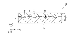
- FIG. 2 is an enlarged view of the silicon carbide substrate shown in FIG. 1 and is a view schematically showing an example of a crystal defect.
- FIG. 3 is a perspective view showing only a base substrate included in the single crystal substrate shown in FIG. 2;
- FIG. 2 is an enlarged view of the silicon carbide substrate shown in FIG. 1 and is a view schematically showing an example of a crystal defect.
- FIG. 2 is an enlarged view of the silicon carbide substrate shown in FIG. 1 and is a view schematically showing an example of a crystal defect.
- FIG. 1 is a longitudinal sectional view of a silicon carbide substrate 10 according to the present embodiment.
- a silicon carbide substrate 10 (an embodiment of a silicon carbide substrate of the present invention) comprises a single crystal substrate 1 (an embodiment of a single crystal substrate of the present invention) and a silicon carbide growth layer 4 deposited on the single crystal substrate 1 ,have.
- the silicon carbide growth layer 4 is used as a semiconductor layer which can form, for example, a power device described later, by taking advantage of the wide band gap and the number of crystal defects.
- this silicon carbide growth layer 4 for example, a semiconductor layer composed of cubic silicon carbide (3C-SiC) can be mentioned. Cubic silicon carbide is particularly preferably used as a wide band gap semiconductor for power devices because the band gap value is as wide as 2.36 eV or more, and the thermal conductivity and the dielectric breakdown electric field are high.
- the silicon carbide growth layer 4 is not limited to the semiconductor layer composed of 3C—SiC, and may be a semiconductor layer composed of 4H—SiC or 6H—SiC.
- a transistor for boost converter, a diode, etc. are mentioned, for example.
- a metal-oxide-semiconductor field-effect transistor (MOSFET), an insulated gate bipolar transistor (IGBT), a Schottky barrier diode (SBD) and the like can be mentioned.
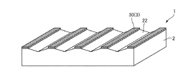
- FIG. 2 is a perspective view showing single crystal substrate 1 included in silicon carbide substrate 10 shown in FIG.
- FIG. 3 is a perspective view showing only the base substrate 2 included in the single crystal substrate 1 shown in FIG.
- Single crystal substrate 1 has base substrate 2 and silicon carbide base film 3 provided on base substrate 2. Such a single crystal substrate 1 is used, for example, as a base for epitaxially growing the silicon carbide growth layer 4 using the silicon carbide base film 3 as a seed layer.
- the base substrate 2 is not particularly limited as long as it is a single crystal substrate, but, for example, these crystals are formed on a silicon substrate, polycrystalline silicon carbide substrate, diamond substrate, sapphire substrate, quartz substrate, or any substrate It is a composite substrate.
- the base substrate 2 preferably contains silicon, polycrystalline silicon carbide or diamond, and is more preferably composed of a crystalline material containing these as a main material. All such base substrates 2 contain cubic crystals, and are suitable as a base for growing silicon carbide. Therefore, by using such base substrate 2, it is possible to form silicon carbide growth layer 4 of higher quality.
- the thickness of base substrate 2 is appropriately set so as to have mechanical strength sufficient to withstand the handling of the step of forming silicon carbide growth layer 4, and preferably about 100 ⁇ m or more and 2 mm or less as an example.
- the base substrate 2 shown in FIG. 1 is, for example, a single crystal silicon substrate whose main surface is a Si (001) surface.
- the lower surface 2a of the base substrate 2 is a flat surface of the Si (001) surface.
- the upper surface 2b of the base substrate 2 includes a plurality of flat surfaces 21 made of Si (001) and a plurality of grooves 22 whose extending direction is the [110] direction. That is, on the upper surface 2b, the plurality of flat surfaces 21 extending in the [110] direction and the plurality of grooves 22 extending in the [110] direction are alternately arranged in the direction orthogonal to the [110] direction. .
- the upper surface 2b has an uneven shape in which a convex portion (peak) having the flat surface 21 as a top surface and a concave portion (valley) formed of the groove 22 are alternately arranged along the [1-10] direction. It is a face.
- the plurality of grooves 22 be parallel to one another, but a deviation about the manufacturing error is acceptable.
- partially non-parallel portions may be included, and may be curved or bent halfway.
- each groove 22 has a V-shaped cross-sectional shape. That is, each groove 22 includes the first crystal surface 221 and the second crystal surface 222 facing the first crystal surface 221 on the inner surface. Each groove 22 extends in the [110] direction while maintaining the V-shaped cross-sectional shape formed of the first crystal surface 221 and the second crystal surface 222.
- that the first crystal surface 221 and the second crystal surface 222 face each other means that both are located on the inner surface of the groove 22 and located on the opposite side to each other across the bottom of the groove 22.
- the opening angle ⁇ of the groove 22, that is, the angle between the first crystal plane 221 and the second crystal plane 222 is more than 70.6 °.
- Grooves 22 having such an opening angle ⁇ efficiently eliminate or reduce crystal defects in silicon carbide crystals when silicon carbide is epitaxially grown on single crystal substrate 1 including grooves 22 on upper surface 2b. be able to. Thereby, a high quality silicon carbide growth layer 4 is obtained.
- FIG. 4 is an enlarged view of the silicon carbide substrate 10 shown in FIG. 1 and is a view schematically showing an example of a crystal defect.
- the first crystal plane 221 and the second crystal plane 222 face each other.
- crystal defects 91 having an end on the first crystal plane 221 progress in parallel with the Si (111) plane.
- crystal defects 92 that originate at the second crystal plane 222 progress in parallel with the Si (1-11) plane.
- the crystal defect 91 and the crystal defect 92 are associated at the junction point 93 and disappear.
- the crystal defects 91 and 92 which progress in different directions can be associated, eliminated or reduced.
- the opening angle ⁇ of the groove 22 is less than the lower limit value, the opening angle ⁇ is too narrow, so the probability that the crystal defects 91 and 92 are associated decreases, and the crystal defects 91 and 92 can not be sufficiently reduced. .
- the opening angle ⁇ of the groove 22 is preferably 100 ° or more and 176 ° or less, more preferably 150 ° or more and 175 ° or less, and still more preferably 166 ° or more and 174 ° or less. Thereby, the crystal defects 91 and 92 can be eliminated or reduced more efficiently. If the opening angle ⁇ of the groove 22 exceeds the upper limit value, the effect of providing the groove 22 diminishes, so the probability that the crystal defects 91 and 92 are associated decreases, and the crystal defects 91 and 92 are sufficiently reduced. May not be reduced.
- the opening angle ⁇ of the groove 22 can be adjusted in accordance with the width of the groove 22, the formation time of the groove 22, and the like.
- the opening angle ⁇ of the groove 22 can be increased by widening the width of the groove 22, and the opening angle ⁇ of the groove 22 can be reduced by narrowing the width of the groove 22.
- the opening angle ⁇ of the groove 22 can be reduced, while the groove 22 can be formed by shortening the formation time. Since 22 can be made shallow, the opening angle ⁇ of the groove 22 can be increased.
- Such a groove 22 extends in the [110] direction as described above. Further, the base substrate 2 has a plurality of grooves 22 which are arranged in the direction orthogonal to the [110] direction.
- the base substrate 2 has a Si (001) plane as the flat surface 21 provided between the adjacent grooves 22.
- the upper surface 2 b of the base substrate 2 becomes a surface on which the grooves 22 can be easily processed, and therefore, the uneven shape in which the flat surfaces 21 and the grooves 22 are alternately and precisely aligned. It becomes the surface which has Such a top surface 2 b can more efficiently eliminate or reduce crystal defects, even when the film thickness of the silicon carbide growth layer 4 grown on the single crystal substrate 1 is thin.
- the flat surface 21 according to the present embodiment is a region for forming the silicon carbide base film 3 described above. That is, by providing flat surface 21, silicon carbide base film 3 can be stably provided adjacent to groove 22. Thereby, when growing silicon carbide growth layer 4 using silicon carbide base film 3 as a seed layer, silicon carbide growth layer 4 can be efficiently and stably grown from silicon carbide base film 3 toward groove 22. As a result, a higher quality silicon carbide growth layer 4 can be obtained.
- the flat surface 21 may be parallel to the lower surface 2a (rear surface) or may not be parallel. In the case of being parallel, it is easy to provide the silicon carbide base film 3 having a uniform thickness with respect to the flat surface 21. Therefore, as to the silicon carbide growth layer 4 grown toward the groove 22, one having few crystal defects is obtained.
- the angle ⁇ between the flat surface 21 and the first crystal surface 221 is preferably larger than the angle between the flat surface 21 and the Si (1-11) surface. Since the Si (1-11) plane is a plane parallel to the crystal defects, the angle between the flat surface 21 and the first crystal plane 221 is larger than the angle with the Si (1-11) plane.
- the angle between the flat surface 21 and the second crystal surface 222 is also the same as the angle between the flat surface 21 and the first crystal surface 221.
- FIG. 1 illustrates an example in which the flat surface 21 is a Si (001) surface
- the flat surface 21 is not limited to this surface, and the Si (001) surface is inclined at a predetermined angle. It may be a plane.
- a plane in which the Si (001) plane is inclined at an angle of more than 0 ° and less than 54.7 ° in the [110] direction can be mentioned.
- the inclination angle from the Si (001) plane is more preferably 1 ° or more and 15 ° or less, and still more preferably 2 ° or more and 10 ° or less.
- the period C of the groove 22 (see FIG. 4), that is, the sum of the width W2 of the groove 22 and the width W1 of the flat surface 21 is not particularly limited, but is preferably 0.1 ⁇ m to 100 ⁇ m, 0.2 ⁇ m It is more preferable that the thickness is not less than 20 ⁇ m.
- the width W2 of the groove 22 is preferably 5% or more and 95% or less of the period C of the groove 22, and more preferably 30% or more and 85% or less.
- the single crystal constituting the base substrate 2 is a cubic crystal, for example, (001) plane, (010) plane, (001) plane, (-100) plane, (0-10) plane, (00- 1)
- the faces and the like are mutually equivalent faces. Therefore, the Si (001) plane in the present specification can be replaced with these equivalent planes. That is, since the Si (001) plane in the present invention is not limited to only that plane, when these equivalent planes are collectively described, it is typically described as a Si ⁇ 100 ⁇ plane.
- the present specification describes that there is a predetermined relationship between the Si (001) plane and other planes and directions, the case where the Si (001) plane is replaced by an equivalent plane is described. Is replaced with other planes and directions so as to maintain the predetermined relationship described above.
- the (111) plane, the (-111) plane, the (1-11) plane, the (11-1) plane, the (-1-11) plane, the (-11-1) plane, etc. are equivalent to each other. It is a good side. Therefore, since the Si (111) plane and the Si (1-11) plane in the specification of the present application can be replaced with these equivalent planes, in the present application, when these equivalent planes are collectively described, Described as Si ⁇ 111 ⁇ plane.
- the [110] direction, the [101] direction, the [011] direction, the [1-10] direction, the [10-1] direction, the [01-1] direction, and the like are mutually equivalent directions. Therefore, since the [110] direction and the [1-10] direction in the present specification can be replaced with these equivalent directions, in the present application, when those equivalent directions are collectively described, ⁇ 110 Describe as> direction.
- the [110] direction or the [1-10] direction and the other surface or direction
- the [110] direction or [1-10] When the direction is replaced with the equivalent direction, the other planes and directions are also replaced so as to maintain the predetermined relationship described above.
- Silicon carbide primer film- Silicon carbide base film 3 is provided on flat surface 21 of upper surface 2 b of base substrate 2.
- the silicon carbide base film 3 may be, for example, a carbonized film formed by modifying the surface of a silicon single crystal substrate, and is a silicon carbide film obtained by forming SiC on the upper surface of the base substrate 2 It is also good.
- silicon carbide base film 3 may be provided only on a part of flat surface 21.
- the crystal structure of the silicon carbide base film 3 is not particularly limited, it is, for example, cubic SiC (3C-SiC). Note that crystals other than 3C-SiC, for example, 4H-SiC, 6H-SiC may be used.
- the thickness of the silicon carbide base film 3 is not particularly limited, but is preferably 1 nm or more and 100 nm or less, more preferably 2 nm or more and 50 nm or less, and still more preferably 3 nm or more and 10 nm or less. By setting the thickness of the silicon carbide base film 3 within the above range, the thickness becomes necessary and sufficient as a seed layer.
- the thickness of silicon carbide base film 3 When the thickness of silicon carbide base film 3 is less than the above lower limit value, the thickness of silicon carbide base film 3 may be insufficient as a seed layer. On the other hand, when the thickness of the silicon carbide base film 3 exceeds the above upper limit, the thickness of the silicon carbide base film 3 becomes too thick, so depending on the conditions of the epitaxial growth, the influence of the silicon carbide base film 3 causes silicon carbide growth. There is a risk of reaching layer 4.
- the thickness of the silicon carbide base film 3 is measured, for example, by a measurement method using an optical method such as ellipsometry, or the cross section of the single crystal substrate 1 is observed with an electron microscope, an optical microscope, etc. It can be determined by a method such as measuring the thickness of silicon carbide base film 3 on the observation image.
- the whole silicon carbide base film 3 is a single crystal, it is not necessarily limited thereto, and may be a polycrystal, a microcrystalline, or an amorphous crystal.
- the silicon carbide base film 3 may be provided in the groove 22 other than on the flat surface 21, that is, at least a part of the first crystal surface 221 and the second crystal surface 222, but preferably the flat surface. It is provided only on 21. As a result, crystals can be grown toward the inside of the grooves 22 with the silicon carbide base film 3 provided at a constant density as a seed layer, so that crystals with fewer crystal defects can be grown. As a result, a higher quality silicon carbide growth layer 4 can be obtained.
- 5 to 9 are views for explaining an embodiment of a method of manufacturing a single crystal substrate according to the present invention.
- a process of preparing a base material with mask 120 including a single crystal base material 100 and a first mask 110 provided on a part of the surface includes the steps of: providing a second mask 30 on the surface of the base material 100; etching the single crystal base material 100 to form a groove 22; and removing the first mask 110.
- the single crystal substrate 1 can be manufactured efficiently. The respective steps will be sequentially described below.
- a single crystal base material 100 is prepared. Since the single crystal base material 100 is a raw material of the base substrate 2, for example, the same single crystal material as the above-described base substrate 2 can be mentioned.
- a mask coating 110 ′ is provided on the surface of the single crystal base material 100.
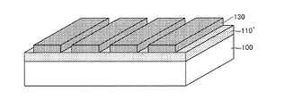
- a mask coating 110 ' is formed to cover the entire surface of the single crystal base material 100 (see FIG. 5).
- the mask coating 110 ′ is made of a material resistant to the etching process of the single crystal base material 100 described later. Examples of such a material include silicon oxide and silicon nitride.
- a photosensitive film is formed on the surface of the mask coating 110 '. Then, patterning is performed by subjecting the photosensitive film to exposure and development processing. Thereby, the resist film 130 provided only in the target area is obtained (see FIG. 5).
- the mask coating 110 ′ is etched through the patterned resist film 130.
- the region of the mask coating 110 ′ not covered by the resist film 130 is etched.
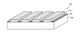
- the first mask 110 provided in the region corresponding to the groove 22 to be formed in the process described later is obtained (see FIG. 6).
- the base material 120 with a mask provided with the single crystal base material 100 and the 1st mask 110 provided in a part of the surface is obtained. Thereafter, the resist film 130 is removed.
- the second mask 30 is formed on the surface of the single crystal base material 100.
- the second mask 30 is formed in a region of the surface of the single crystal base material 100 which is not covered by the first mask 110.
- the second mask 30 may be formed on the surface of the first mask 110, but is omitted in FIG.
- the method of forming the second mask 30 is not particularly limited. For example, a method of forming the surface of the single crystal base material 100 by modifying (carbonizing), forming silicon carbide on the upper surface of the single crystal base material 100 And the like.
- the carbonization treatment is performed by heating the single crystal base material 100 in a carbon-based gas atmosphere. According to the carbonization process, since a part of the single crystal base material 100 is converted to silicon carbide, it is possible to form the second mask 30 having high crystallinity as compared with other methods.
- the carbon-based gas atmosphere is formed of a processing gas containing a carbon-based gas.
- the carbon-based gas is not limited as long as it is a gas containing carbon, for example, ethylene (C 2 H 4 ), acetylene (C 2 H 2 ), propane (C 3 H 8 ) and methane (CH 4 ) Hydrocarbon gas such as ethane (C 2 H 6 ), normal butane (n-C 4 H 10 ), isobutane (i-C 4 H 10 ), neopentane (neo-C 5 H 12 ), etc. One or two or more of them can be used in combination.
- the mixed gas of these hydrocarbon type gas and other gas may be sufficient.
- examples of other gases include hydrogen silicide gas, silicon chloride gas, silicon carbide gas and the like.
- any gas such as a carrier gas may be mixed with these process gases.
- the carrier gas include hydrogen, nitrogen, helium, argon and the like.
- the concentration of the carbon-based gas in the processing gas is suitably set according to the speed of the carbonization treatment and the like, but is preferably 0.1% by volume or more and 30% by volume or less, as an example. More preferably, it is 0.3% by volume or more and 5% by volume or less.
- the heating temperature of the single crystal base material 100 in the carbonization treatment is preferably 500 ° C. or more and 1400 ° C. or less, more preferably 800 ° C. or more and 1300 ° C. or less, and still more preferably 950 ° C. or more and 1200 ° C. or less .
- the heating time of the single crystal base material 100 in the carbonization treatment is preferably 0.5 minutes or more, preferably 1 minute to 120 minutes, and more preferably 3 minutes. More preferably, it is 90 minutes or less.
- the heating conditions within the above range, it is possible to form the second mask 30 having the thickness as described above.
- the conversion rate to silicon carbide is optimized, so that the second mask 30 of good quality can be formed.
- the carbonization may be performed in any of normal pressure atmosphere, pressurized atmosphere, and reduced pressure atmosphere, but preferably in a state where the processing gas is introduced while exhausting the processing chamber containing the single crystal base material 100. You should do it.
- the introduction amount of the carbon-based gas in the processing gas is 10 sccm or more and 100 sccm or less.
- a vapor phase film forming method such as a CVD method or a vapor deposition method is used.
- the single crystal base material 100 is etched. Thereby, the groove 22 is formed. In this etching process, the upper surface of the single crystal base material 100 is etched so as to remove the lower side of the first mask 110 (the region facing the first mask 110).
- etching process for example, a process of heating the mask-attached base material 120 provided with the second mask 30 above the sublimation temperature of Si can be mentioned.
- Si atoms contained in the single crystal base material 100 easily sublime, and are discharged to the outside from the gap between the single crystal base material 100 and the first mask 110.
- the lower part of the first mask 110 is etched to form a groove 22 as shown in FIG.
- the heating temperature is slightly different depending on the pressure of the space in which the single crystal base material 100 is placed, etc., but is a temperature at which Si atoms can be sublimed and not higher than the melting point of Si, and is 900.degree. The range is sufficient. Moreover, although heating time is suitably set according to the said heating temperature, it is preferable that time exposed to heating temperature is 0.5 to 60 minutes.
- the heating of the mask-attached base material 120 may be performed in a normal pressure atmosphere or a pressurized atmosphere, but is preferably performed in a reduced pressure atmosphere or a reducing atmosphere. Thereby, the sublimation of Si atoms is promoted or oxidation is prevented, so that the etching process can be performed while suppressing the denaturation of the single crystal base material 100.
- the pressure of the reduced pressure atmosphere is not particularly limited as long as it is less than the atmospheric pressure, and is, for example, 0.5 Pa or less.
- the groove 22 is formed below the first mask 110.
- the etching is suppressed in the region where the second mask 30 is formed. For this reason, the flat surface 21 described above is formed in this region.
- a process of exposing the mask attached base material 120 provided with the second mask 30 to an etching gas may be used instead of the above heat treatment.
- the first mask 110 is removed.
- an etching process is used to remove the first mask 110.
- the single crystal substrate 1 shown in FIG. 9 is obtained.
- the second mask 30 shown in FIG. 9 can be used as the silicon carbide base film 3 shown in FIG. 1 described above. Therefore, the second mask 30 may be removed but may be left without being removed.
- Silicon carbide substrate 10 is manufactured by epitaxially growing silicon carbide growth layer 4 on single crystal substrate 1.
- Silicon carbide base film 3 functions as a seed layer for epitaxially growing silicon carbide growth layer 4.
- the silicon carbide growth layer 4 grows the silicon carbide base film 3 as a seed layer by, for example, housing the single crystal substrate 1 in a processing chamber and heating the single crystal substrate 1 while introducing a source gas. As a result, silicon carbide substrate 10 shown in FIG. 1 is obtained.
- a mixed gas obtained by mixing a gas containing carbon and a gas containing silicon at a predetermined ratio, a gas containing carbon and silicon at a predetermined ratio, a gas containing carbon and a gas containing carbon
- a mixed gas comprising a mixture of a gas containing silicon and a gas containing carbon and silicon in a predetermined ratio.
- the gas containing carbon for example, other than ethylene (C 2 H 4 ), acetylene (C 2 H 2 ), propane (C 3 H 8 ), methane (CH 4 ), ethane (C 2 H 6) ), Normal butane (n-C 4 H 10 ), isobutane (i-C 4 H 10 ), neopentane (neo-C 5 H 12 ), etc., and one or more of these may be used in combination. It can be used.
- ethylene C 2 H 4
- acetylene C 2 H 2
- propane C 3 H 8
- methane CH 4
- ethane C 2 H 6
- Normal butane n-C 4 H 10
- isobutane i-C 4 H 10
- neopentane neo-C 5 H 12
- the gas containing silicon for example, monosilane (SiH 4 ), disilane (Si 2 H 6 ), trisilane (Si 3 H 8 ), tetrasilane (Si 4 H 10 ), dichlorosilane (SiH 2 Cl 2 ), Tetrachlorosilane (SiCl 4 ), trichlorosilane (SiHCl 3 ), hexachlorodisilane (Si 2 Cl 6 ), and the like can be mentioned, and one or more of these can be used in combination.
- methylsilane (SiH 3 CH 3 ), dimethylsilane (SiH 2 (CH 3 ) 2 ), trimethylsilane (SiH (CH 3 ) 3 ) and the like can be mentioned. It is possible to use one kind or two or more kinds in combination.
- the heating temperature in epitaxial growth that is, the temperature of single crystal substrate 1 during epitaxial growth is preferably 600 ° C. or more and 1400 ° C. or less, more preferably 800 ° C. or more and 1350 ° C. or less, and 950 ° C. or more and 1100 ° C. It is further preferred that The heating time in the epitaxial growth is appropriately set in accordance with the intended thickness of the silicon carbide growth layer 4.
- the pressure in the processing chamber in the epitaxial growth is not particularly limited, but is preferably 1 ⁇ 10 ⁇ 4 Pa or more and atmospheric pressure (100 kPa) or less, and more preferably 1 ⁇ 10 ⁇ 3 Pa or more and 10 kPa or less.
- Such a high quality silicon carbide substrate 10 is suitably used, for example, as a semiconductor substrate capable of producing high-performance power devices.
- the single crystal substrate, the method for manufacturing a single crystal substrate, and the silicon carbide substrate according to the present invention have been described above based on the illustrated embodiments, but the present invention is not limited to this.
- the single crystal substrate and the silicon carbide substrate according to the present invention may each be obtained by adding an arbitrary element to the above-described embodiment.
- an arbitrary step may be added to the embodiment described above.
- a mask coating was formed on the entire surface of the silicon wafer. Subsequently, a resist film was formed on the mask film, and then the mask film was etched. Thereby, a base material with a mask having a first mask patterned in a target shape was obtained.
- a second mask was formed on the surface of the mask-attached base material.
- ethylene gas was used, and the surface of the silicon wafer was carbonized by heating at 1000 ° C. for 60 minutes.
- the base material with mask provided with the second mask was etched.
- a base substrate in which grooves extending in the [011] direction and flat surfaces were alternately arranged was obtained.
- the mask base material was heated at 1000 ° C. for 30 minutes in a reduced pressure atmosphere.
- a silicon carbide growth layer was epitaxially grown on the obtained single crystal substrate.
- a silicon carbide substrate was obtained.
- a silicon carbide growth layer was obtained by heating at 1000 ° C. for 2 hours using ethylene gas and dichlorosilane gas as source gases.
- Example 2 A silicon carbide substrate was obtained in the same manner as in Example 1 except that the manufacturing conditions were changed as shown in Table 1 or Table 2.
- Example 4 A silicon carbide substrate was obtained in the same manner as in Example 1 except that the groove formation process was omitted.
- the silicon carbide substrate obtained in each example was found to have a relatively low density of crystal defects. From this, it was recognized that according to the present invention, a high quality silicon carbide growth layer can be manufactured.
Landscapes
- Chemical & Material Sciences (AREA)
- Engineering & Computer Science (AREA)
- Materials Engineering (AREA)
- Metallurgy (AREA)
- Organic Chemistry (AREA)
- Crystallography & Structural Chemistry (AREA)
- Inorganic Chemistry (AREA)
- General Chemical & Material Sciences (AREA)
- Chemical Kinetics & Catalysis (AREA)
- Mechanical Engineering (AREA)
- Crystals, And After-Treatments Of Crystals (AREA)
Abstract
結晶欠陥の少ない炭化ケイ素成長層を形成可能な単結晶基板、かかる単結晶基板を効率よく製造可能な単結晶基板の製造方法、および、高品質な炭化ケイ素成長層を有する炭化ケイ素基板を提供すること。 第1結晶面と、前記第1結晶面と対向する第2結晶面と、を内面に含み、延在方向が<110>方向である溝を複数備える下地基板を有し、前記第1結晶面と前記第2結晶面とのなす角度が70.6°超であることを特徴とする単結晶基板。また、前記第1結晶面と前記第2結晶面とのなす角度が100°以上176°以下であることが好ましい。
Description
本発明は、単結晶基板、単結晶基板の製造方法および炭化ケイ素基板に関するものである。
炭化ケイ素(SiC)は、Siに比べ2倍以上のバンドギャップ(2.36~3.23eV)を有するワイドバンドギャップ半導体であり、高耐圧デバイス用材料として注目されている。
ところが、SiCは、Siとは異なり、結晶化温度が高温であるため、Si基板と同様の液相からの引上げ法による単結晶インゴット作成が困難である。そのため、昇華法によりSiCの単結晶インゴットを形成する方法が提案されているが、かかる昇華法においては、大口径で結晶欠陥の少ない基板を形成することが非常に難しい。一方、SiC結晶の中でも立方晶SiC(3C-SiC)は、比較的低温で形成可能であるため、基板上にエピタキシャル成長を行う方法が提案されている。
このエピタキシャル成長を用いたSiC基板の製造方法の1つとして、気相中において、Si基板上に3C-SiCを成長させるヘテロエピタキシャル技術が検討されている。例えば、非特許文献1には、Si(100)基板において[001]方向を[110]方向へ4°程度傾けてなるオフセット基板を用い、その表面上にSiCをエピタキシャル成長させることが開示されている。これにより、SiC成長層において、反位相領域界面(APB : Anti-phase boundary)と呼ばれる結晶欠陥の低減を図ることができる。
また、特許文献1には、(001)面の底部と、(111)面、(-1-11)面、(-111)面および(1-11)面からなるファセットと、を含む溝を備える半導体基板と、半導体基板上に設けられた半導体緩衝層と、半導体緩衝層上に設けられた第1の半導体層と、を有する半導体装置が開示されている。
Journal of Crystal Growth 78 (1986) 538-544.
ところが、従来のオフセット基板や溝を備えた半導体基板では、結晶欠陥の低減を十分に図ることができない。
本発明の目的は、結晶欠陥の少ない炭化ケイ素成長層を形成可能な単結晶基板、かかる単結晶基板を効率よく製造可能な単結晶基板の製造方法、および、高品質な炭化ケイ素成長層を有する炭化ケイ素基板を提供することにある。
上記目的は、下記の本発明により達成される。
本発明の単結晶基板は、第1結晶面と、前記第1結晶面と対向する第2結晶面と、を内面に含み、延在方向が<110>方向である溝を複数備える下地基板を有し、
前記第1結晶面と前記第2結晶面とのなす角度が70.6°超であることを特徴とする。
本発明の単結晶基板は、第1結晶面と、前記第1結晶面と対向する第2結晶面と、を内面に含み、延在方向が<110>方向である溝を複数備える下地基板を有し、
前記第1結晶面と前記第2結晶面とのなす角度が70.6°超であることを特徴とする。
これにより、溝を含む単結晶基板を下地にして炭化ケイ素をエピタキシャル成長させたとき、炭化ケイ素結晶内における結晶欠陥を効率よく消滅または低減させることができる。したがって、結晶欠陥の少ない炭化ケイ素成長層を形成可能な単結晶基板が得られる。
本発明の単結晶基板では、前記第1結晶面と前記第2結晶面とのなす角度が100°以上176°以下であることが好ましい。
これにより、結晶欠陥をより効率よく消滅または低減させることができる。
これにより、結晶欠陥をより効率よく消滅または低減させることができる。
本発明の単結晶基板では、前記下地基板は、さらに、前記溝同士の間に設けられている平坦面としてSi{100}面を備えることが好ましい。
これにより、平坦面と溝とを高精度に形成することができるので、炭化ケイ素下地膜から溝に向かって炭化ケイ素成長層を効率よく安定的に成長させることができる。その結果、成長させる炭化ケイ素成長層が薄い場合でも、結晶欠陥をより効率よく消滅または低減させることができる。
本発明の単結晶基板では、前記下地基板は、さらに、前記溝同士の間に設けられている平坦面としてSi{100}面が<110>方向に0°超54.7°未満の角度で傾斜している面を備えることが好ましい。
これにより、溝のみならず、平坦面においても、結晶欠陥を消滅または低減させることができる。その結果、より結晶欠陥が少なく、高品質な炭化ケイ素成長層を形成することができる。
本発明の単結晶基板では、前記平坦面と前記第1結晶面とのなす角度は、前記平坦面とSi{111}面とのなす角度よりも大きい角度であることが好ましい。
これにより、結晶欠陥同士をより高い確率で会合させ、消滅または低減させることができる。
本発明の単結晶基板では、さらに、前記平坦面上に設けられている炭化ケイ素下地膜を有することが好ましい。
これにより、単結晶基板上に炭化ケイ素成長層を成長させるとき、炭化ケイ素下地膜をシード層として溝に向かって結晶を成長させることができる。その結果、より高品質な炭化ケイ素成長層が得られる。
本発明の単結晶基板では、前記下地基板は、シリコン、多結晶炭化ケイ素またはダイヤモンドを含むことが好ましい。
これにより、より高品質な炭化ケイ素成長層を形成することができる。
これにより、より高品質な炭化ケイ素成長層を形成することができる。
本発明の単結晶基板の製造方法は、本発明の単結晶基板を製造する方法であって、
単結晶母材とその表面の一部に設けられている第1マスクとを備えるマスク付き母材を用意する工程と、
前記単結晶母材の表面に第2マスクを設ける工程と、
前記単結晶母材にエッチング処理を施し、前記単結晶母材の表面のうち前記第1マスクに臨む領域に前記溝を形成する工程と、
前記第1マスクを除去する工程と、を有することを特徴とする。
これにより、単結晶基板を効率よく製造することができる。
単結晶母材とその表面の一部に設けられている第1マスクとを備えるマスク付き母材を用意する工程と、
前記単結晶母材の表面に第2マスクを設ける工程と、
前記単結晶母材にエッチング処理を施し、前記単結晶母材の表面のうち前記第1マスクに臨む領域に前記溝を形成する工程と、
前記第1マスクを除去する工程と、を有することを特徴とする。
これにより、単結晶基板を効率よく製造することができる。
本発明の炭化ケイ素基板では、本発明の単結晶基板と、
前記単結晶基板上に成膜されている炭化ケイ素成長層と、を有することを特徴とする。
前記単結晶基板上に成膜されている炭化ケイ素成長層と、を有することを特徴とする。
これにより、炭化ケイ素成長層のワイドバンドギャップと結晶欠陥の少なさとを活かし、パワーデバイスを形成し得る半導体層を備えた炭化ケイ素基板が得られる。
以下、単結晶基板、単結晶基板の製造方法および炭化ケイ素基板を添付図面に示す好適実施形態に基づいて詳細に説明する。
<炭化ケイ素基板>
まず、本発明の炭化ケイ素基板の実施形態について説明する。
図1は、本実施形態に係る炭化ケイ素基板10の縦断面図である。
まず、本発明の炭化ケイ素基板の実施形態について説明する。
図1は、本実施形態に係る炭化ケイ素基板10の縦断面図である。
炭化ケイ素基板10(本発明の炭化ケイ素基板の実施形態)は、単結晶基板1(本発明の単結晶基板の実施形態)と、単結晶基板1上に成膜された炭化ケイ素成長層4と、を有している。この炭化ケイ素成長層4は、そのワイドバンドギャップと結晶欠陥の少なさとを活かし、例えば後述するパワーデバイスを形成し得る半導体層として用いられる。
かかる炭化ケイ素成長層4としては、例えば、立方晶炭化ケイ素(3C-SiC)で構成された半導体層が挙げられる。立方晶炭化ケイ素は、バンドギャップ値が2.36eV以上と広く、熱伝導率や絶縁破壊電界が高いため、パワーデバイス用のワイドバンドギャップ半導体として特に好適に用いられる。なお、炭化ケイ素成長層4は、3C-SiCで構成された半導体層に限定されず、4H-SiCや6H-SiCで構成された半導体層であってもよい。
そして、後述する単結晶基板1を用いることにより、結晶欠陥が少なく高品質な炭化ケイ素成長層4を形成することができる。
なお、炭化ケイ素基板10を用いて製造されるパワーデバイスとしては、例えば昇圧コンバーター用のトランジスターやダイオード等が挙げられる。具体的には、MOSFET(metal-oxide-semiconductor field-effect transistor)、絶縁ゲート型バイポーラー・トランジスター(IGBT)、ショットキーバリアーダイオード(SBD)等が挙げられる。
以下、単結晶基板1についてさらに詳述する。
(単結晶基板)
図2は、図1に示す炭化ケイ素基板10に含まれる単結晶基板1を示す斜視図である。また、図3は、図2に示す単結晶基板1に含まれる下地基板2のみを示す斜視図である。
(単結晶基板)
図2は、図1に示す炭化ケイ素基板10に含まれる単結晶基板1を示す斜視図である。また、図3は、図2に示す単結晶基板1に含まれる下地基板2のみを示す斜視図である。
単結晶基板1は、下地基板2と、下地基板2上に設けられた炭化ケイ素下地膜3と、を有している。このような単結晶基板1は、例えば、炭化ケイ素下地膜3をシード層として炭化ケイ素成長層4をエピタキシャル成長させるための下地として用いられる。
-下地基板-
下地基板2は、単結晶の基板であれば、特に限定されないが、例えば、シリコン基板、多結晶炭化ケイ素基板、ダイヤモンド基板、サファイア基板、石英基板、または任意の基板にこれらの結晶を成膜した複合基板である。
下地基板2は、単結晶の基板であれば、特に限定されないが、例えば、シリコン基板、多結晶炭化ケイ素基板、ダイヤモンド基板、サファイア基板、石英基板、または任意の基板にこれらの結晶を成膜した複合基板である。
このうち、下地基板2は、シリコン、多結晶炭化ケイ素またはダイヤモンドを含むことが好ましく、これらを主材料とする結晶材料で構成されるのがより好ましい。このような下地基板2は、いずれも立方晶を含み、炭化ケイ素を成長させるための下地として好適なものである。このため、かかる下地基板2を用いることにより、より高品質な炭化ケイ素成長層4を形成させることができる。
下地基板2の厚さは、炭化ケイ素成長層4を形成する工程のハンドリングに耐え得る程度の機械的強度を有するように適宜設定されるが、一例として100μm以上2mm以下程度が好ましい。
図1に示す下地基板2には、一例として、主面がSi(001)面の単結晶シリコン基板を挙げている。そして、下地基板2の下面2aは、Si(001)面の平坦面となっている。一方、下地基板2の上面2bは、Si(001)面からなる複数の平坦面21と、延在方向が[110]方向である複数の溝22と、を含んでいる。すなわち、上面2bでは、[110]方向に延在する複数の平坦面21と、[110]方向に延在する複数の溝22とが、[110]方向と直交する方向に交互に並んでいる。これにより、上面2bは、平坦面21を頂面とする凸部(山)と、溝22からなる凹部(谷)とが、[1-10]方向に沿って交互に並んだ凹凸形状を有する面になっている。
なお、複数の溝22は、互いに平行であることが好ましいが、製造誤差程度のずれは許容される。また、部分的に非平行な部分が含まれていてもよく、途中で湾曲または屈曲していてもよい。
ここで、各溝22は、横断面形状がV字状になっている。すなわち、各溝22は、第1結晶面221と、この第1結晶面221と対向する第2結晶面222と、を内面に含んでいる。そして、各溝22は、このような第1結晶面221と第2結晶面222とで構成されるV字状の横断面形状を維持しながら、[110]方向に延在している。なお、第1結晶面221と第2結晶面222とが対向しているとは、双方が溝22の内面に位置するとともに、溝22の底を挟んで互いに反対側に位置していることをいう。
また、溝22の開口角θ、すなわち、第1結晶面221と第2結晶面222とのなす角度は、70.6°超である。このような開口角θを有する溝22は、その溝22を上面2bに含む単結晶基板1を下地にして炭化ケイ素をエピタキシャル成長させたとき、炭化ケイ素結晶内における結晶欠陥を効率よく消滅または低減させることができる。これにより、高品質な炭化ケイ素成長層4が得られる。
ここで、図4は、図1に示す炭化ケイ素基板10の拡大図であって、結晶欠陥の一例を模式的に示した図である。
溝22では、前述したように、第1結晶面221と第2結晶面222とが互いに向かい合っている。図4に示す例では、第1結晶面221に端を発する結晶欠陥91が、Si(111)面と平行に進展している。一方、第2結晶面222に端を発する結晶欠陥92は、Si(1-11)面と平行に進展している。そして、結晶欠陥91と結晶欠陥92は、会合点93において会合し、消滅している。このように、溝22を有する単結晶基板1上に成長させた炭化ケイ素成長層4では、互いに異なる方向に進展する結晶欠陥91、92を会合させ、消滅または減少させることができる。
なお、溝22の開口角θが前記下限値を下回ると、開口角θが狭すぎるため、結晶欠陥91、92が会合する確率が低下し、結晶欠陥91、92を十分に低減することができない。
また、溝22の開口角θは、100°以上176°以下であるのが好ましく、150°以上175°以下であるのがより好ましく、166°以上174°以下であるのがさらに好ましい。これにより、結晶欠陥91、92をより効率よく消滅または低減させることができる。なお、溝22の開口角θが前記上限値を上回ると、溝22を設けたことによる効果が薄れてしまうため、結晶欠陥91、92が会合する確率が低下し、結晶欠陥91、92を十分に低減させることができないおそれがある。
溝22の開口角θは、溝22の幅や溝22の形成時間等に応じて調整可能である。例えば、溝22の幅を広くすることにより、溝22の開口角θを大きくすることができ、一方、溝22の幅を狭くすることにより、溝22の開口角θを小さくすることができる。また、溝22の形成時間を長くすることにより、溝22を深くすることができるので、溝22の開口角θを小さくすることができ、一方、溝22の形成時間を短くすることにより、溝22を浅くすることができるので、溝22の開口角θを大きくすることができる。
このような溝22は、前述したように、[110]方向に延在している。また、下地基板2は、複数の溝22を有しており、これらは[110]方向と直交する方向に並んでいる。
一方、本実施形態に係る下地基板2は、前述したように、隣接する溝22同士の間に設けられている平坦面21としてSi(001)面を有している。このような平坦面21が設けられることにより、下地基板2の上面2bは、溝22を加工し易い面となるため、平坦面21と溝22とが交互にかつ高精度に並んでなる凹凸形状を有する面となる。このような上面2bは、単結晶基板1上に成長させる炭化ケイ素成長層4の膜厚が薄い場合でも、結晶欠陥をより効率よく消滅または低減させることができる。
また、本実施形態に係る平坦面21は、前述した炭化ケイ素下地膜3を成膜するための領域となる。すなわち、平坦面21が設けられることにより、溝22に隣接して炭化ケイ素下地膜3を安定的に設けることができる。これにより、炭化ケイ素下地膜3をシード層として炭化ケイ素成長層4を成長させるとき、炭化ケイ素下地膜3から溝22に向かって炭化ケイ素成長層4を効率よく安定的に成長させることができる。その結果、より高品質な炭化ケイ素成長層4が得られる。
なお、平坦面21は、下面2a(裏面)と平行であってもよく、非平行であってもよい。平行である場合には、平坦面21に対して均一な厚さの炭化ケイ素下地膜3を設け易いため、溝22に向かって成長する炭化ケイ素成長層4についても、結晶欠陥の少ないものが得られる。
また、平坦面21と第1結晶面221とのなす角度αは、平坦面21とSi(1-11)面とのなす角度よりも大きいことが好ましい。Si(1-11)面は、結晶欠陥と平行な面であるため、平坦面21と第1結晶面221とのなす角度を、Si(1-11)面とのなす角度よりも大きい角度に設定することで、結晶欠陥同士をより高い確率で会合させ、消滅または低減させることができる。
また、平坦面21と第2結晶面222とのなす角度も、平坦面21と第1結晶面221とのなす角度と同様である。
また、図1では、平坦面21がSi(001)面である例を図示しているが、平坦面21はこの面に限定されず、Si(001)面が所定の角度で傾斜している面であってもよい。一例として、Si(001)面が[110]方向に0°超54.7°未満の角度で傾斜している面が挙げられる。このように傾斜させた面を平坦面21とすることにより、溝22のみならず、平坦面21においても、結晶欠陥を消滅または低減させることができる。その結果、より結晶欠陥が少なく、高品質な炭化ケイ素成長層4を形成することができる。
なお、Si(001)面からの傾斜角度は、1°以上15°以下であるのがより好ましく、2°以上10°以下であるのがさらに好ましい。これにより、上記効果がより顕著になり、炭化ケイ素成長層4のさらなる高品質化が図られる。
溝22の周期C(図4参照)は、すなわち溝22の幅W2と平坦面21の幅W1との合計は、特に限定されないが、0.1μm以上100μm以下であるのが好ましく、0.2μm以上20μm以下であるのがより好ましい。溝22の周期Cを前記範囲内に設定することにより、単結晶基板1上に成長させる炭化ケイ素成長層4の膜厚が薄い場合でも、結晶欠陥をより効率よく消滅または低減させることができる。
また、溝22の幅W2は、溝22の周期Cの5%以上95%以下であるのが好ましく、30%以上85%以下であるのがより好ましい。溝22の周期Cに対する溝22の幅W2の割合を前記範囲内に設定することにより、溝22の幅W2と平坦面21の幅W1とのバランスが最適化される。その結果、単結晶基板1上に成長させる炭化ケイ素成長層4の膜厚が薄い場合でも、結晶欠陥をより効率よく消滅または低減させることができる。
また、下地基板2を構成する単結晶が立方晶である場合、例えば、(001)面、(010)面、(001)面、(-100)面、(0-10)面、(00-1)面等は、互いに等価な面である。したがって、本願明細書におけるSi(001)面は、これらの等価な面に置き換え得る。すなわち、本願発明におけるSi(001)面は、その面のみに限定されるものではないことから、これらの等価な面をまとめて記載する場合に、代表的にSi{100}面と記載する。なお、本願明細書ではSi(001)面とその他の面や方向との間に所定の関係があることを記載しているが、Si(001)面がそれと等価な面に置き換えられた場合には、前述した所定の関係が維持されるように、その他の面や方向についても置き換えられることとなる。
同様に、例えば、(111)面、(-111)面、(1-11)面、(11-1)面、(-1-11)面、(-11-1)面等は、互いに等価な面である。したがって、本願明細書におけるSi(111)面やSi(1-11)面は、これらの等価な面に置き換え得るため、本願では、これらの等価な面をまとめて記載する場合に、代表的にSi{111}面と記載する。なお、本願明細書ではSi(111)面やSi(1-11)面とその他の面や方向との間に所定の関係があることを記載しているが、Si(111)面やSi(1-11)面がそれと等価な面に置き換えられた場合には、前述した所定の関係が維持されるように、その他の面や方向についても置き換えられることとなる。
同様に、例えば、[110]方向、[101]方向、[011]方向、[1-10]方向、[10-1]方向、[01-1]方向等は、互いに等価な方向である。したがって、本願明細書における[110]方向や[1-10]方向は、これらの等価な方向に置き換え得るため、本願では、これらの等価な方向をまとめて記載する場合に、代表的に<110>方向と記載する。なお、本願明細書では、[110]方向や[1-10]方向とその他の面や方向との間に所定の関係があることを記載しているが、[110]方向や[1-10]方向がそれと等価な方向に置き換えられた場合には、前述した所定の関係が維持されるように、その他の面や方向についても置き換えられることとなる。
-炭化ケイ素下地膜-
炭化ケイ素下地膜3は、下地基板2の上面2bのうち、平坦面21上に設けられている。この炭化ケイ素下地膜3は、例えばシリコン単結晶基板の表面を改質してなる炭化膜であってもよく、下地基板2の上面にSiCを成膜して得られた炭化ケイ素膜であってもよい。また、炭化ケイ素下地膜3は、平坦面21のうちの一部のみに設けられていてもよい。
炭化ケイ素下地膜3は、下地基板2の上面2bのうち、平坦面21上に設けられている。この炭化ケイ素下地膜3は、例えばシリコン単結晶基板の表面を改質してなる炭化膜であってもよく、下地基板2の上面にSiCを成膜して得られた炭化ケイ素膜であってもよい。また、炭化ケイ素下地膜3は、平坦面21のうちの一部のみに設けられていてもよい。
炭化ケイ素下地膜3の結晶構造は、特に限定されないが、例えば、立方晶SiC(3C-SiC)とされる。なお、3C-SiC以外の結晶、例えば、4H-SiC、6H-SiCであってもよい。
また、炭化ケイ素下地膜3の厚さは、特に限定されないが、1nm以上100nm以下であるのが好ましく、2nm以上50nm以下であるのがより好ましく、3nm以上10nm以下であるのがさらに好ましい。炭化ケイ素下地膜3の厚さを前記範囲内に設定することにより、シード層として必要かつ十分な厚さとなる。
なお、炭化ケイ素下地膜3の厚さが前記下限値を下回ると、炭化ケイ素下地膜3の厚さがシード層として不十分になるおそれがある。一方、炭化ケイ素下地膜3の厚さが前記上限値を上回ると、炭化ケイ素下地膜3の厚さが厚くなり過ぎるため、エピタキシャル成長の条件等によっては、炭化ケイ素下地膜3の影響が炭化ケイ素成長層4に及んでしまうおそれがある。
また、炭化ケイ素下地膜3の厚さは、例えば、エリプソメトリ法等の光学的手法を用いた測定法により計測する、あるいは、単結晶基板1の断面を電子顕微鏡や光学顕微鏡等で観察し、観察像上において炭化ケイ素下地膜3の厚さを計測する、等の方法によって求められる。
また、炭化ケイ素下地膜3は、その全体が単結晶であることが好ましいが、必ずしもそれに限定されず、多結晶、微結晶、アモルファス晶であってもよい。
なお、炭化ケイ素下地膜3は、平坦面21上の他、溝22内、すなわち第1結晶面221および第2結晶面222の少なくとも一部にも設けられていてもよいが、好ましくは平坦面21上のみに設けられる。これにより、一定の密度で設けられた炭化ケイ素下地膜3をシード層として、溝22内に向かって結晶を成長させることができるので、結晶欠陥のより少ない結晶を成長させることができる。その結果、より高品質な炭化ケイ素成長層4を得ることができる。
<単結晶基板の製造方法>
次に、本発明の単結晶基板の製造方法の実施形態について説明する。
次に、本発明の単結晶基板の製造方法の実施形態について説明する。
図5~図9は、それぞれ本発明の単結晶基板の製造方法の実施形態を説明するための図である。
本実施形態に係る単結晶基板1の製造方法は、単結晶母材100とその表面の一部に設けられている第1マスク110とを備えるマスク付き母材120を用意する工程と、単結晶母材100の表面に第2マスク30を設ける工程と、単結晶母材100にエッチング処理を施し、溝22を形成する工程と、第1マスク110を除去する工程と、を有する。このような製造方法によれば、単結晶基板1を効率よく製造することができる。以下、各工程について順次説明する。
[1]まず、単結晶母材100を用意する。単結晶母材100は、下地基板2の原料となるため、例えば、前述した下地基板2と同様の単結晶材料が挙げられる。
次いで、単結晶母材100の表面にマスク用被膜110’を設ける。ここでは、まず、単結晶母材100の表面全体を覆うようにマスク用被膜110’を成膜する(図5参照)。マスク用被膜110’は、後述する単結晶母材100のエッチング処理において耐性を有する材料で構成される。かかる材料としては、例えば、酸化ケイ素、窒化ケイ素等が挙げられる。
次に、マスク用被膜110’の表面に感光性を有する被膜を形成する。そして、この感光性被膜に露光・現像処理を施すことにより、パターニングを施す。これにより、目的とする領域のみに設けられたレジスト膜130が得られる(図5参照)。
次に、パターニングされたレジスト膜130を介してマスク用被膜110’にエッチング処理を施す。これにより、マスク用被膜110’のうち、レジスト膜130に覆われていない領域がエッチングされる。その結果、後述する工程において形成しようとする溝22に対応する領域に設けられた第1マスク110が得られる(図6参照)。そして、単結晶母材100とその表面の一部に設けられた第1マスク110とを備えるマスク付き母材120が得られる。
その後、レジスト膜130を除去する。
その後、レジスト膜130を除去する。
[2]次に、図7に示すように、単結晶母材100の表面に第2マスク30を形成する。この第2マスク30は、単結晶母材100の表面のうち第1マスク110で覆われていない領域に形成される。なお、第2マスク30は、第1マスク110の表面に形成されてもよいが、図7では省略している。
第2マスク30の形成方法は、特に限定されないが、例えば、単結晶母材100の表面を改質(炭化処理)することによって形成する方法、単結晶母材100の上面に炭化ケイ素を成膜して形成する方法等が挙げられる。
炭化処理は、炭素系ガス雰囲気中で単結晶母材100を加熱することにより行われる。炭化処理によれば、単結晶母材100の一部を炭化ケイ素に転化させるため、他の方法と比較して結晶性の高い第2マスク30を形成することができる。
炭素系ガス雰囲気は、炭素系ガスを含む処理ガスで構成される。炭素系ガスとしては、炭素を含むガスであれば限定されないものの、例えば、エチレン(C2H4)の他、アセチレン(C2H2)、プロパン(C3H8)、メタン(CH4)、エタン(C2H6)、ノルマルブタン(n-C4H10)、イソブタン(i-C4H10)、ネオペンタン(neo-C5H12)等の炭化水素系ガスが挙げられ、これらのうちの1種または2種以上を組み合わせて用いることができる。
また、これらの炭化水素系ガスとその他のガスとの混合ガスであってもよい。その他のガスとしては、例えば、ケイ化水素系ガス、塩化ケイ素系ガス、炭化ケイ素系ガス等が挙げられる。
さらに、これらの処理ガスに対して、キャリアガス等の任意のガスが混合されてもよい。キャリアガスとしては、例えば、水素、窒素、ヘリウム、アルゴン等が挙げられる。キャリアガスが用いられる場合、処理ガス中の炭素系ガスの濃度は、炭化処理の速度等に応じて適宜設定されるものの、一例として0.1体積%以上30体積%以下であるのが好ましく、0.3体積%以上5体積%以下であるのがより好ましい。
炭化処理における単結晶母材100の加熱温度は、500℃以上1400℃以下であるのが好ましく、800℃以上1300℃以下であるのがより好ましく、950℃以上1200℃以下であるのがさらに好ましい。また、炭化処理における単結晶母材100の加熱時間は、前記加熱温度に曝される時間が0.5分以上であるのが好ましく、1分以上120分以下であるのがより好ましく、3分以上90分以下であるのがさらに好ましい。
加熱条件を前記範囲内に設定することにより、前述したような厚さの第2マスク30を形成することができる。また、付加される熱エネルギーを最適化することによって、炭化ケイ素への転化速度が最適化されるため、良質な第2マスク30を形成することができる。
また、炭化処理は、常圧雰囲気、加圧雰囲気または減圧雰囲気のいずれで行われてもよいが、好ましくは単結晶母材100を納めた処理室内を排気しつつ、処理ガスを導入した状態で行うようにすればよい。一例として、処理ガス中の炭素系ガスの導入量は、10sccm以上100sccm以下とされる。
一方、炭化ケイ素の成膜処理では、例えばCVD法、蒸着法のような気相成膜法が用いられる。
[3]次に、単結晶母材100にエッチング処理を施す。これにより溝22を形成する。
このエッチング処理では、単結晶母材100の上面のうち、第1マスク110の下方(第1マスク110に臨む領域)が除去されるようにエッチングされる。
このエッチング処理では、単結晶母材100の上面のうち、第1マスク110の下方(第1マスク110に臨む領域)が除去されるようにエッチングされる。
このようなエッチング処理としては、例えば、第2マスク30を設けたマスク付き母材120をSiの昇華温度以上で加熱する処理が挙げられる。これにより、単結晶母材100に含まれるSi原子が昇華し易くなり、単結晶母材100と第1マスク110との隙間から外部に排出される。その結果、第1マスク110の下方がエッチングされ、図8に示すような溝22が形成される。
なお、加熱温度は、単結晶母材100が置かれる空間の圧力等に応じて若干異なるものの、Si原子が昇華し得る温度でかつSiの融点以下の温度とされ、900℃以上1400℃以下の範囲であればよい。また、加熱時間は前記加熱温度に応じて適時設定されるが、加熱温度に曝される時間が0.5分以上60分以下であることが好ましい。
また、マスク付き母材120の加熱は、常圧雰囲気や加圧雰囲気において行われてもよいが、減圧雰囲気または還元雰囲気において行うことが好ましい。これにより、Si原子の昇華が促進されたり、酸化が防止されるため、単結晶母材100の変性を抑えつつエッチング処理を施すことができる。
この減圧雰囲気の圧力は大気圧未満であれば特に限定されないが、例えば0.5Pa以下とされる。
以上のようにして、第1マスク110の下方に溝22が形成される。
以上のようにして、第1マスク110の下方に溝22が形成される。
なお、単結晶母材100の上面のうち、第2マスク30が成膜されている領域では、エッチングが抑制される。このため、この領域には前述した平坦面21が形成されることとなる。
また、エッチング処理では、上記の加熱処理に代えて、第2マスク30を設けたマスク付き母材120をエッチングガスに曝す処理が用いられてもよい。
[4]次に、第1マスク110を除去する。
第1マスク110の除去には、例えばエッチング処理が用いられる。
第1マスク110の除去には、例えばエッチング処理が用いられる。
以上のようにして図9に示す単結晶基板1が得られる。なお、図9に示す第2マスク30は、前述した図1に示す炭化ケイ素下地膜3として用いることができる。このため、第2マスク30については、除去されてもよいが、除去されることなく残すようにしてもよい。
<炭化ケイ素基板の製造方法>
次に、図1に示す炭化ケイ素基板10を製造する方法の一例について説明する。
次に、図1に示す炭化ケイ素基板10を製造する方法の一例について説明する。
炭化ケイ素基板10は、単結晶基板1上に炭化ケイ素成長層4をエピタキシャル成長させることで製造される。炭化ケイ素下地膜3は、炭化ケイ素成長層4をエピタキシャル成長させるためのシード層として機能する。
炭化ケイ素成長層4は、例えば処理室内に単結晶基板1を収納し、原料ガスを導入しつつ単結晶基板1を加熱することにより、炭化ケイ素下地膜3をシード層として成長する。その結果、図1に示す炭化ケイ素基板10が得られる。
原料ガスとしては、炭素を含むガスとケイ素を含むガスとを所定の割合にて混合してなる混合ガス、炭素とケイ素とを所定の割合で含む炭素およびケイ素を含むガス、炭素を含むガスとケイ素を含むガスと炭素およびケイ素を含むガスとを所定の割合にて混合してなる複数種混合ガスが挙げられる。
このうち、炭素を含むガスとしては、例えば、エチレン(C2H4)の他、アセチレン(C2H2)、プロパン(C3H8)、メタン(CH4)、エタン(C2H6)、ノルマルブタン(n-C4H10)、イソブタン(i-C4H10)、ネオペンタン(neo-C5H12)等が挙げられ、これらのうちの1種または2種以上を組み合わせて用いることができる。
また、ケイ素を含むガスとしては、例えば、モノシラン(SiH4)、ジシラン(Si2H6)、トリシラン(Si3H8)、テトラシラン(Si4H10)、ジクロロシラン(SiH2Cl2)、テトラクロロシラン(SiCl4)、トリクロロシラン(SiHCl3)、ヘキサクロロジシラン(Si2Cl6)等が挙げられ、これらのうちの1種または2種以上を組み合わせて用いることができる。
さらに、炭素およびケイ素を含むガスとしては、メチルシラン(SiH3CH3)、ジメチルシラン(SiH2(CH3)2)、トリメチルシラン(SiH(CH3)3)等が挙げられ、これらのうちの1種または2種以上を組み合わせて用いることができる。
また、エピタキシャル成長における加熱温度、すなわち、エピタキシャル成長時の単結晶基板1の温度は、600℃以上1400℃以下であるのが好ましく、800℃以上1350℃以下であるのがより好ましく、950℃以上1100℃以下であるのがさらに好ましい。なお、エピタキシャル成長における加熱時間は、炭化ケイ素成長層4の目的とする厚さに応じて適宜設定される。
また、エピタキシャル成長における処理室内の圧力は、特に限定されないが、1×10⁻⁴Pa以上大気圧(100kPa)以下であるのが好ましく、1×10⁻³Pa以上10kPa以下であるのがより好ましい。
以上のようにして炭化ケイ素下地膜3上に炭化ケイ素成長層4をエピタキシャル成長させることにより、高品質な炭化ケイ素成長層4を有する炭化ケイ素基板10を効率よく得ることができる。
このような高品質な炭化ケイ素基板10は、例えば高性能のパワーデバイスを製造可能な半導体基板として好適に用いられる。
以上、本発明に係る単結晶基板、単結晶基板の製造方法および炭化ケイ素基板を、図示の実施形態に基づいて説明したが、本発明はこれに限定されるものではない。例えば、本発明に係る単結晶基板および炭化ケイ素基板は、それぞれ、上述した実施形態に任意の要素が付加されたものであってもよい。また、本発明に係る単結晶基板の製造方法は、上述した実施形態に任意の工程が追加されたものであってもよい。
次に、本発明の具体的実施例について説明する。
1.炭化ケイ素基板の製造
(実施例1)
<1>まず、単結晶母材としてSi(001)面を主面とする6インチ(直径150mm、厚さ0.625mm)のシリコンウエハーを用意した。そして、表面をフッ酸等で洗浄した。
1.炭化ケイ素基板の製造
(実施例1)
<1>まず、単結晶母材としてSi(001)面を主面とする6インチ(直径150mm、厚さ0.625mm)のシリコンウエハーを用意した。そして、表面をフッ酸等で洗浄した。
次に、シリコンウエハーの全面にマスク用被膜を成膜した。続いて、マスク用被膜上にレジスト膜を形成した後、マスク用被膜をエッチングした。これにより、目的とする形状にパターニングされた第1マスクを有するマスク付き母材を得た。
<2>次に、マスク付き母材の表面に第2マスクを形成した。なお、第2マスクの形成ではエチレンガスを使用し、1000℃で60分間加熱することにより、シリコンウエハーの表面を炭化させる処理を行った。
<3>次に、第2マスクを設けたマスク付き母材にエッチング処理を施した。これにより、[011]方向に延在する溝と平坦面とが交互に並んだ下地基板を得た。このエッチング処理では、減圧雰囲気においてマスク付き母材を1000℃で30分間加熱する処理を行った。
<4>次に、エッチング処理により第1マスクを除去した。これにより、下地基板と第2マスクとを備える単結晶基板を得た。
<5>次に、得られた単結晶基板上に炭化ケイ素成長層をエピタキシャル成長させた。これにより、炭化ケイ素基板を得た。なお、エピタキシャル成長では、原料ガスとしてエチレンガスおよびジクロロシランガスを使用し、1000℃で2時間加熱することにより、炭化ケイ素成長層を得るようにした。
(実施例2~21)
製造条件を表1または表2に示すように変更した以外は、実施例1と同様にして炭化ケイ素基板を得た。
製造条件を表1または表2に示すように変更した以外は、実施例1と同様にして炭化ケイ素基板を得た。
(比較例1~3)
製造条件を表1に示すように変更した以外は、実施例1と同様にして炭化ケイ素基板を得た。
製造条件を表1に示すように変更した以外は、実施例1と同様にして炭化ケイ素基板を得た。
(比較例4)
溝の形成プロセスを省略した以外は、実施例1と同様にして炭化ケイ素基板を得た。
溝の形成プロセスを省略した以外は、実施例1と同様にして炭化ケイ素基板を得た。
2.炭化ケイ素基板の評価
各実施例および各比較例で得られた炭化ケイ素基板について、結晶欠陥の密度を測定した。なお、結晶欠陥の密度は、炭化ケイ素基板の中心部の表面を原子間力顕微鏡(AFM : Atomic Force Microscope)で観察することにより測定した。
各実施例および各比較例で得られた炭化ケイ素基板について、結晶欠陥の密度を測定した。なお、結晶欠陥の密度は、炭化ケイ素基板の中心部の表面を原子間力顕微鏡(AFM : Atomic Force Microscope)で観察することにより測定した。
次いで、比較例4で得られた炭化ケイ素基板の結晶欠陥の密度を1としたとき、各実施例および各比較例で得られた炭化ケイ素基板の結晶欠陥の密度の相対値を算出した。そして、算出結果を以下の評価基準に照らして評価した。
<結晶欠陥の密度の評価基準>
◎:結晶欠陥の密度の相対値が0.5未満である
○:結晶欠陥の密度の相対値が0.5以上0.75未満である
△:結晶欠陥の密度の相対値が0.75以上1未満である
×:結晶欠陥の密度の相対値が1以上である
評価結果を表1、2に示す。
◎:結晶欠陥の密度の相対値が0.5未満である
○:結晶欠陥の密度の相対値が0.5以上0.75未満である
△:結晶欠陥の密度の相対値が0.75以上1未満である
×:結晶欠陥の密度の相対値が1以上である
評価結果を表1、2に示す。
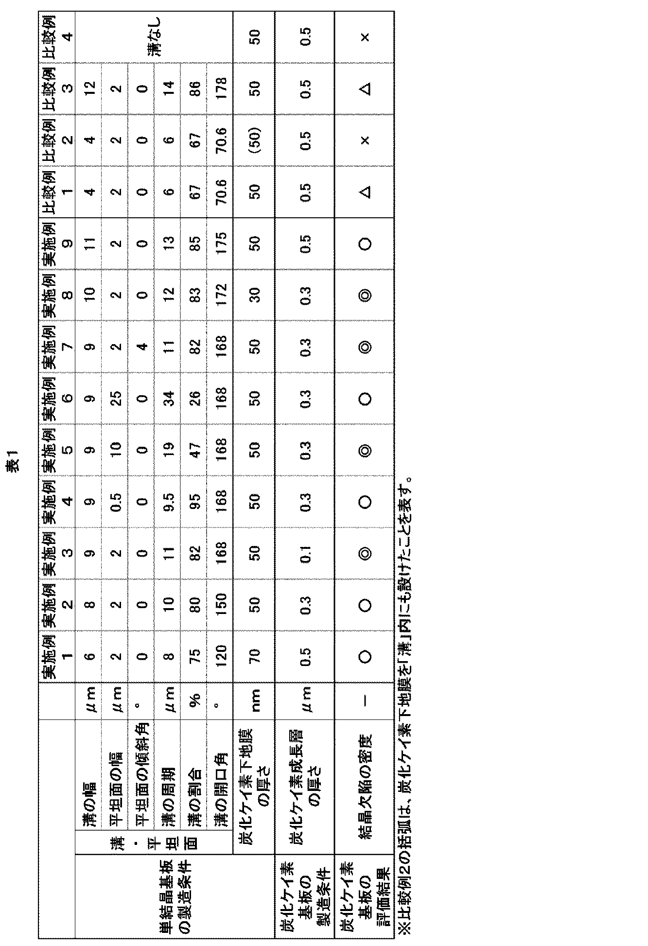
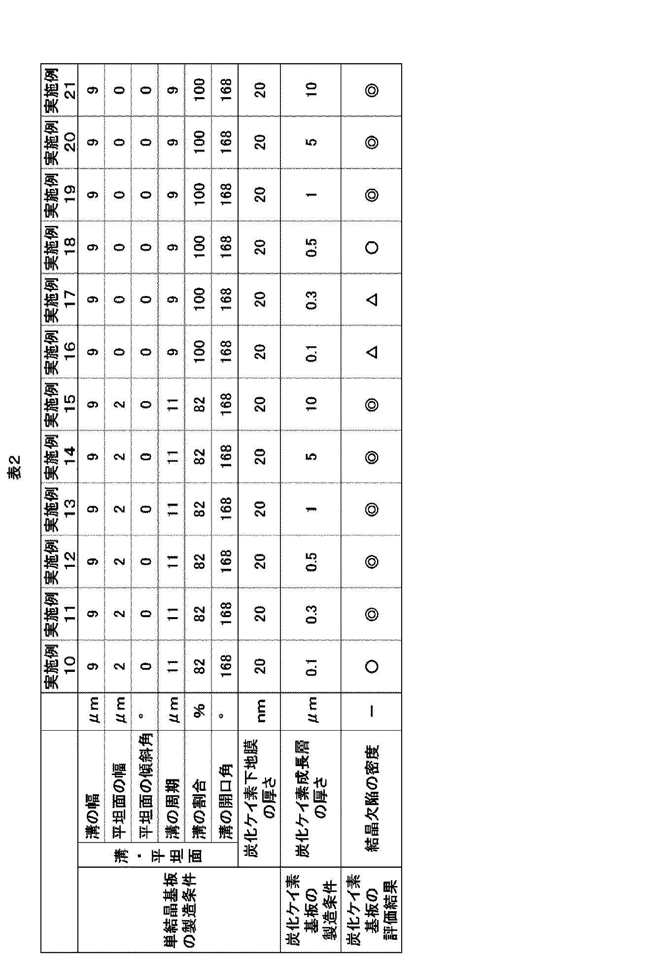
表1から明らかなように、各実施例で得られた炭化ケイ素基板は、結晶欠陥の密度が相対的に低いことが認められた。このことから、本発明によれば、高品質な炭化ケイ素成長層を製造し得ることが認められた。
また、表2から明らかなように、平坦面を設けた単結晶基板では、平坦面を設けない単結晶基板に比べて、エピタキシャル成長させる炭化ケイ素成長層が薄い場合でも、結晶欠陥を抑えられることが認められた。
1…単結晶基板、2…下地基板、2a…下面、2b…上面、3…炭化ケイ素下地膜、4…炭化ケイ素成長層、10…炭化ケイ素基板、21…平坦面、22…溝、30…第2マスク、91…結晶欠陥、92…結晶欠陥、93…会合点、100…単結晶母材、110…マスク、110’…マスク用被膜、120…マスク付き母材、130…レジスト膜、221…第1結晶面、222…第2結晶面、C…周期、W1…幅、W2…幅、α…角度、θ…開口角
Claims (9)
- 第1結晶面と前記第1結晶面と対向する第2結晶面とを内面に含み、延在方向が<110>方向である溝を複数備える下地基板を有し、
前記第1結晶面と前記第2結晶面とのなす角度が70.6°超であることを特徴とする単結晶基板。 - 前記第1結晶面と前記第2結晶面とのなす角度が100°以上176°以下である請求項1に記載の単結晶基板。
- 前記下地基板は、さらに、前記溝同士の間に設けられている平坦面としてSi{100}面を備える請求項1または2に記載の単結晶基板。
- 前記下地基板は、さらに、前記溝同士の間に設けられている平坦面としてSi{100}面が<110>方向に0°超54.7°未満の角度で傾斜している面を備える請求項1または2に記載の単結晶基板。
- 前記平坦面と前記第1結晶面とのなす角度は、前記平坦面とSi{111}面とのなす角度よりも大きい角度である請求項3または4に記載の単結晶基板。
- さらに、前記平坦面上に設けられている炭化ケイ素下地膜を有する請求項3ないし5のいずれか1項に記載の単結晶基板。
- 前記下地基板は、シリコン、多結晶炭化ケイ素またはダイヤモンドを含む請求項1ないし6のいずれか1項に記載の単結晶基板。
- 請求項1ないし7のいずれか1項に記載の単結晶基板を製造する方法であって、
単結晶母材とその表面の一部に設けられている第1マスクとを備えるマスク付き母材を用意する工程と、
前記単結晶母材の表面に第2マスクを設ける工程と、
前記単結晶母材にエッチング処理を施し、前記単結晶母材の表面のうち前記第1マスクに臨む領域に前記溝を形成する工程と、
前記第1マスクを除去する工程と、を有することを特徴とする単結晶基板の製造方法。 - 請求項1ないし7のいずれか1項に記載の単結晶基板と、
前記単結晶基板上に成膜されている炭化ケイ素成長層と、を有することを特徴とする炭化ケイ素基板。
Priority Applications (1)
| Application Number | Priority Date | Filing Date | Title |
|---|---|---|---|
| US16/628,785 US11142821B2 (en) | 2017-07-07 | 2018-06-28 | Method for producing single crystal substrate having a plurality of grooves using a pair of masks |
Applications Claiming Priority (2)
| Application Number | Priority Date | Filing Date | Title |
|---|---|---|---|
| JP2017-133415 | 2017-07-07 | ||
| JP2017133415A JP6958041B2 (ja) | 2017-07-07 | 2017-07-07 | 単結晶基板、単結晶基板の製造方法および炭化ケイ素基板 |
Publications (1)
| Publication Number | Publication Date |
|---|---|
| WO2019009182A1 true WO2019009182A1 (ja) | 2019-01-10 |
Family
ID=64950096
Family Applications (1)
| Application Number | Title | Priority Date | Filing Date |
|---|---|---|---|
| PCT/JP2018/024615 Ceased WO2019009182A1 (ja) | 2017-07-07 | 2018-06-28 | 単結晶基板、単結晶基板の製造方法および炭化ケイ素基板 |
Country Status (3)
| Country | Link |
|---|---|
| US (1) | US11142821B2 (ja) |
| JP (1) | JP6958041B2 (ja) |
| WO (1) | WO2019009182A1 (ja) |
Families Citing this family (1)
| Publication number | Priority date | Publication date | Assignee | Title |
|---|---|---|---|---|
| US20240047207A1 (en) * | 2022-08-02 | 2024-02-08 | Infineon Technologies Ag | Technique for Forming Cubic Silicon Carbide and Heterojunction Silicon Carbide Device |
Citations (2)
| Publication number | Priority date | Publication date | Assignee | Title |
|---|---|---|---|---|
| JP2004189598A (ja) * | 1998-10-10 | 2004-07-08 | Hoya Corp | 炭化珪素膜及びその製造方法 |
| JP2006196631A (ja) * | 2005-01-13 | 2006-07-27 | Hitachi Ltd | 半導体装置及びその製造方法 |
Family Cites Families (2)
| Publication number | Priority date | Publication date | Assignee | Title |
|---|---|---|---|---|
| EP1130135B1 (en) | 1999-10-08 | 2007-08-08 | Hoya Corporation | Silicon carbide film and method for manufacturing the same |
| US6475456B2 (en) * | 2000-02-29 | 2002-11-05 | Hoya Corporation | Silicon carbide film and method for manufacturing the same |
-
2017
- 2017-07-07 JP JP2017133415A patent/JP6958041B2/ja active Active
-
2018
- 2018-06-28 WO PCT/JP2018/024615 patent/WO2019009182A1/ja not_active Ceased
- 2018-06-28 US US16/628,785 patent/US11142821B2/en active Active
Patent Citations (2)
| Publication number | Priority date | Publication date | Assignee | Title |
|---|---|---|---|---|
| JP2004189598A (ja) * | 1998-10-10 | 2004-07-08 | Hoya Corp | 炭化珪素膜及びその製造方法 |
| JP2006196631A (ja) * | 2005-01-13 | 2006-07-27 | Hitachi Ltd | 半導体装置及びその製造方法 |
Also Published As
| Publication number | Publication date |
|---|---|
| JP6958041B2 (ja) | 2021-11-02 |
| US20200140998A1 (en) | 2020-05-07 |
| JP2019014626A (ja) | 2019-01-31 |
| US11142821B2 (en) | 2021-10-12 |
Similar Documents
| Publication | Publication Date | Title |
|---|---|---|
| US11404269B2 (en) | Single crystal substrate with undulating ridges and silicon carbide substrate | |
| JP6248532B2 (ja) | 3C−SiCエピタキシャル層の製造方法、3C−SiCエピタキシャル基板および半導体装置 | |
| CN106169497B (zh) | 碳化硅基板以及碳化硅基板的制造方法 | |
| JP2025011298A (ja) | 炭化ケイ素半導体エピタキシャル基板 | |
| Niu et al. | The influence of temperature on the silicon droplet evolution in the homoepitaxial growth of 4H-SiC | |
| US9362368B2 (en) | Substrate with silicon carbide film, method for producing substrate with silicon carbide film, and semiconductor device | |
| JP2006321696A (ja) | 炭化珪素単結晶の製造方法 | |
| JP2003282451A (ja) | SiC単結晶薄膜の作製法 | |
| JP6958041B2 (ja) | 単結晶基板、単結晶基板の製造方法および炭化ケイ素基板 | |
| JP2016092399A (ja) | 炭化ケイ素膜付き基板、炭化ケイ素膜付き基板の製造方法、及び、半導体装置 | |
| JP6958042B2 (ja) | 単結晶基板、単結晶基板の製造方法および炭化ケイ素基板 | |
| US9536954B2 (en) | Substrate with silicon carbide film, semiconductor device, and method for producing substrate with silicon carbide film | |
| JP7322408B2 (ja) | 炭化珪素多結晶基板、炭化珪素多結晶膜の製造方法および炭化珪素多結晶基板の製造方法 | |
| JP2013035731A (ja) | 単結晶炭化シリコン膜の製造方法及び単結晶炭化シリコン膜付き基板の製造方法 | |
| JP2014033068A (ja) | 炭化珪素半導体装置の製造方法および炭化珪素基板 | |
| JP2019014628A (ja) | 炭化ケイ素膜付き基板の製造方法、炭化ケイ素膜付き基板および炭化ケイ素単結晶基板 | |
| JP2015078094A (ja) | SiC層の形成方法、3C−SiCエピタキシャル基板の製造方法、および3C−SiCエピタキシャル基板 | |
| JP7711575B2 (ja) | 単結晶ダイヤモンド膜の形成方法 | |
| JP6627304B2 (ja) | 炭化ケイ素膜付き基板、半導体装置および炭化ケイ素膜付き基板の製造方法 | |
| JP5267271B2 (ja) | 半導体基板の製造方法及び半導体基板 | |
| CN112602171A (zh) | 外延基板 | |
| JP2018070435A (ja) | 半導体基板の製造方法 | |
| JP2016023117A (ja) | 立方晶炭化珪素半導体基板、および立方晶炭化珪素半導体基板の製造方法 |
Legal Events
| Date | Code | Title | Description |
|---|---|---|---|
| 121 | Ep: the epo has been informed by wipo that ep was designated in this application |
Ref document number: 18828544 Country of ref document: EP Kind code of ref document: A1 |
|
| NENP | Non-entry into the national phase |
Ref country code: DE |
|
| 122 | Ep: pct application non-entry in european phase |
Ref document number: 18828544 Country of ref document: EP Kind code of ref document: A1 |