WO2018235676A1 - ソケット及び検査治具 - Google Patents
ソケット及び検査治具 Download PDFInfo
- Publication number
- WO2018235676A1 WO2018235676A1 PCT/JP2018/022431 JP2018022431W WO2018235676A1 WO 2018235676 A1 WO2018235676 A1 WO 2018235676A1 JP 2018022431 W JP2018022431 W JP 2018022431W WO 2018235676 A1 WO2018235676 A1 WO 2018235676A1
- Authority
- WO
- WIPO (PCT)
- Prior art keywords
- insulating support
- socket
- inspection
- recess
- contact probe
- Prior art date
- Legal status (The legal status is an assumption and is not a legal conclusion. Google has not performed a legal analysis and makes no representation as to the accuracy of the status listed.)
- Ceased
Links
Images






Classifications
-
- G—PHYSICS
- G01—MEASURING; TESTING
- G01R—MEASURING ELECTRIC VARIABLES; MEASURING MAGNETIC VARIABLES
- G01R1/00—Details of instruments or arrangements of the types included in groups G01R5/00 - G01R13/00 and G01R31/00
- G01R1/02—General constructional details
- G01R1/06—Measuring leads; Measuring probes
- G01R1/067—Measuring probes
-
- G—PHYSICS
- G01—MEASURING; TESTING
- G01R—MEASURING ELECTRIC VARIABLES; MEASURING MAGNETIC VARIABLES
- G01R31/00—Arrangements for testing electric properties; Arrangements for locating electric faults; Arrangements for electrical testing characterised by what is being tested not provided for elsewhere
- G01R31/26—Testing of individual semiconductor devices
-
- H—ELECTRICITY
- H01—ELECTRIC ELEMENTS
- H01R—ELECTRICALLY-CONDUCTIVE CONNECTIONS; STRUCTURAL ASSOCIATIONS OF A PLURALITY OF MUTUALLY-INSULATED ELECTRICAL CONNECTING ELEMENTS; COUPLING DEVICES; CURRENT COLLECTORS
- H01R13/00—Details of coupling devices of the kinds covered by groups H01R12/70 or H01R24/00 - H01R33/00
- H01R13/46—Bases; Cases
- H01R13/52—Dustproof, splashproof, drip-proof, waterproof, or flameproof cases
-
- H—ELECTRICITY
- H01—ELECTRIC ELEMENTS
- H01R—ELECTRICALLY-CONDUCTIVE CONNECTIONS; STRUCTURAL ASSOCIATIONS OF A PLURALITY OF MUTUALLY-INSULATED ELECTRICAL CONNECTING ELEMENTS; COUPLING DEVICES; CURRENT COLLECTORS
- H01R33/00—Coupling devices specially adapted for supporting apparatus and having one part acting as a holder providing support and electrical connection via a counterpart which is structurally associated with the apparatus, e.g. lamp holders; Separate parts thereof
- H01R33/74—Devices having four or more poles, e.g. holders for compact fluorescent lamps
- H01R33/76—Holders with sockets, clips, or analogous contacts adapted for axially-sliding engagement with parallely-arranged pins, blades, or analogous contacts on counterpart, e.g. electronic tube socket
Definitions
- the present invention relates to a socket and an inspection jig provided with a contact probe for inspecting a semiconductor or the like.
- FIG. 11 is a schematic enlarged sectional view of a socket and inspection jig according to the prior art
- FIG. 12 is a plan view
- FIG. 13 is a sectional view taken along line XIII-XIII in FIG. 12
- FIG. 14 is a sectional view taken along line XIV-XIV in FIG.
- FIG. 16 is a bottom view of the side view.
- the socket 50 comprises an insulating support 60 and a plurality of contact probes 20.
- the insulating support 60 is composed of a pin block 61, a pin plate 62, and a guide 63.
- the insulating support 60 supports a plurality of contact probes 20.
- the guide 63 guides and positions a semiconductor (IC, LSI or the like) 40 as an inspection object to a predetermined measurement position.
- the inspection jig 70 includes a socket 50 and an inspection substrate 30 (a substrate for connecting the contact probe 20 and the measuring device).
- the inspection substrate 30 is closely fixed to the substrate mounting surface of the insulating support 60.
- the first plunger 21 of the contact probe 20 is electrically connected to the electrode 41 of the semiconductor 40.
- the second plunger 22 of the contact probe 20 is electrically connected to the electrode 31 of the inspection substrate 30. Since the electrodes 31 of the inspection substrate 30 are electrically connected to the measuring device, the electrodes 41 of the semiconductor 40 are electrically connected to the measuring device via the inspection jig 70.
- a ventilation gap S2 is provided between the pin block 61 and the pin plate 62.
- the ventilation gap S2 is open at the side surface of the insulating support 60.
- no ventilation means is provided between the pin plate 62 and the inspection substrate 30.
- a socket 50 for semiconductor inspection and an inspection jig 70 are also used in a temperature test environment.
- the inspection substrate 30 is attached to the test tank so that the socket 50 of the inspection jig 70 is on the inner side of the test tank.
- the inspection substrate 30 serves as a wall that divides the internal atmosphere of the test tank from the outside air.
- the problem is that the socket 50, the contact probe 20, and the inspection substrate 30 cause dew condensation or frost-dew by changing the state of the temperature test tank from high temperature (normal temperature) ⁇ low temperature ⁇ high temperature (normal temperature) ⁇ low temperature etc. , Frost is generated.
- Condensation, frost dew, and frost are generated due to the change in the amount of saturated water vapor as the temperature changes and the water vapor becoming liquid or solidified.
- the standard of each temperature condition in a temperature test is high temperature> 50 ° C, normal temperature 25 25 ° C, low temperature ⁇ 0 ° C.
- Condensation and frost may be generated not only by the temperature change of the test tank but also by the temperature change of the contact probe itself due to the energization of the contact probe 20. Further, in this temperature test tank, the inspection substrate itself serves as a shield between the outside air and the temperature test tank without using a heat insulating material. For this reason, dew condensation or frost may occur on the inspection substrate 30 due to the temperature difference between the outside air and the temperature test tank.
- Leakage will occur if condensation, frost, or frost is introduced into the installation surface between the inspection substrate 30 and the socket 50, or into the gap between the plunger 22 of the contact probe 20 and the socket hole (through hole 62a of the pin plate 62). (Failure in which minute current flows) and short circuit failure (short circuit failure) may occur. In addition, when the water freezes in a low temperature state, an open defect (a defect that the plunger can not move) may occur (for example, area A in FIG. 11).
- the water in the entire apparatus is temporarily removed by bringing the entire temperature test tank into a high temperature and dry state before the start of the temperature test.
- water is removed by removing the socket or the inspection substrate and leaving it in a high-temperature dry state for a long time. According to these methods, immediately after dehumidifying and drying, no problem occurs in contact performance.
- moisture may be deposited inside the device, and a leak failure, a short failure and an open failure may occur again.
- Patent Document 1 JP-A-2016-207511 Patent Document 1 is an example of a semiconductor inspection socket.
- Leakage, short-circuit, or open defects may occur if condensation, frost dew, or frost from the temperature test enter the installation surface between the inspection substrate and socket or the gap between the contact probe plunger and the socket hole. is there.
- An object of the present invention is to provide a socket and inspection jig which can eliminate the inconvenience caused by moisture and stabilize the electrical connection between the contact probe and the electrode of the inspection substrate.
- the socket comprises a contact probe and an insulating support that supports the contact probe.
- a recess is provided on the inspection substrate mounting side of the insulating support.
- the contact probe projects into the recess.
- the recess opens on the side surface of the insulating support.
- the surface of the insulating support on which the inspection substrate is mounted is different from the side surface of the insulating support.
- the recess may be a blowing path.
- a hygroscopic material or a heat insulating material may be disposed in the recess.
- the height difference between the surface of the insulating support in contact with the inspection substrate and the bottom of the recess may be 0.15 mm or more and 0.2 mm or less.
- the inspection jig includes a contact probe, an insulating support for supporting the contact probe, and an inspection substrate mounted on the insulating support.
- the recessed part is provided in the board
- the contact probe projects into the recess.
- the recess opens on the side surface of the insulating support.
- the surface of the insulating support on which the inspection substrate is mounted is different from the side surface of the insulating support.
- the recessed portion from which the plunger of the contact probe protrudes is provided on the inspection substrate mounting side of the insulating support that supports the contact probe. Since the recess communicates with the outside air, the inconvenience due to moisture can be eliminated, and the electrical connection between the contact probe and the electrode of the inspection substrate is stabilized.
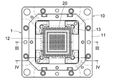
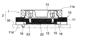
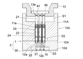
- FIG. 2 is a plan view of Embodiment 1; III-III sectional drawing of FIG. IV-IV sectional drawing of FIG.
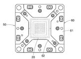
- FIG. 2 is a side view of the first embodiment. The same bottom view.
- FIG. 7 is a schematic enlarged cross-sectional view for explaining the operation and effect of the first embodiment.
- FIG. 10 is a schematic enlarged cross-sectional view showing Embodiment 3 of the present invention.
- FIG. 10 is a schematic enlarged cross-sectional view showing Embodiment 4 of the present invention.
- Embodiment 1 1 is a schematic enlarged sectional view showing Embodiment 1 of the socket and inspection jig according to the present invention
- FIG. 2 is a plan view
- FIG. 3 is a III-III sectional view of FIG. 2 and FIG. IV sectional view
- FIG. 5 is a side view
- FIG. 6 is a bottom view
- FIG. 7 is a schematic enlarged sectional view explaining the operation and effect.
- the socket 1 comprises an insulating support 10 and a plurality of contact probes 20.
- the insulating support 10 has a structure in which the pin block 11, the pin plate 12 and the guide 13 are integrated.
- the insulating support 10 supports a plurality of contact probes 20.
- the inspection jig 2 includes a socket 1 and an inspection substrate 30 mounted on the opposite side of the guide 13 of the insulating support 10.
- the inspection substrate 30 is closely fixed to the substrate mounting surface 11 d of the insulating support 10.
- a ventilation gap S3 is formed between the insulating support 10 and the inspection substrate 30.
- the contact probe 20 has a tube 23 of conductive metal, a first plunger 21, a second plunger 22, and a coil spring 24.
- the first plunger 21 is provided at one end of a tube 23 of conductive metal.
- the second plunger 22 is provided at the other end of the conductive metal tube 23.
- the coil spring 24 is provided in a tube 23 of conductive metal. The coil spring 24 biases the first plunger 21 and the second plunger 22 away from each other. The tips of the first plunger 21 and the second plunger 22 respectively project from both ends of the tube 23.
- the guide 13 of the insulating support 10 guides and positions a semiconductor (IC, LSI or the like) 40 as an inspection object to a predetermined measurement position.
- the guide 13 of the insulating support 10 is movably held by the guide holding portion 11e of the pin block 11 on one side of the pin block 11 within the range of the gap S1.
- the pin block 11 and the pin plate 12 have through holes 11a and 12a.
- the pin block 11 and the pin plate 12 hold the contact probes 20 disposed in the through holes 11 a and 12 a so as not to come off.
- Through holes 13 a corresponding to the through holes 11 a and 12 a are formed in the guide 13.
- the guide 13 moves in the direction in which the gap S1 is reduced so as to press the electrode 41 of the semiconductor 40 against the first plunger 21.
- the semiconductor 40 is held from above by a holding member (not shown) and held by the guide 13.
- a recess 11b for disposing the pin plate 12 is formed on the other side of the pin block 11.
- the pin plate 12 is disposed and fixed in the recess 11 b.
- a ventilation gap S2 is formed between the pin block 11 and the pin plate 12.
- the ventilation gap S2 is open at the side surface of the insulating support 10.
- a ventilation gap S2 is provided for dehumidification around the through holes 11a and 12a and the tube 23.
- the pin block 11 has a substrate mounting surface 11 d for attaching the inspection substrate 30 in close contact.
- the depth from the substrate mounting surface 11 d to the pin plate mounting surface 11 c of the recess 11 b (depth in the axial direction of the contact probe 20) is larger than the thickness of the pin plate 12.
- the recessed part 15 which the 2nd plunger 22 protrudes is provided in the arrangement
- the ventilation gap S3 is opened at the side surface of the insulating support 10, as shown in FIG.
- the side surface of the insulating support 10 is a surface which intersects the substrate mounting surface 11 d among a plurality of surfaces constituting the insulating support 10 and is an outer surface other than the substrate mounting surface 11 d.
- positioning pins 16 are erected and fixed on the substrate mounting surface 11 d of the pin block 11.
- the positioning pins 16 are fitted in the positioning holes of the inspection substrate 30, whereby the inspection substrate 30 is positioned and fixed on the substrate mounting surface 11d of the pin block 11 (that is, the substrate mounting surface of the insulating support 10).
- the height difference between the substrate mounting surface 11d of the insulating support 10 in contact with the inspection substrate 30 and the bottom surface of the recess 15 (the opposite surface 12b of the pin plate 12 to the inspection substrate 30) is 0.15 mm or more. It is set to .2 mm or less.
- the height difference is determined in consideration of the stroke and the like of the second plunger 22. However, if it is less than 0.15 mm, the ventilation effect is small, and if it is larger than 0.2 mm, the positioning accuracy of the second plunger 22 is degraded.
- the semiconductor 40 is held from above by a holding member (not shown) and held by the guide 13.
- the first plunger 21 of the contact probe 20 is electrically connected to the electrode 41 of the semiconductor 40.
- the second plunger 22 of the contact probe 20 is electrically connected to the electrode 31 of the inspection substrate 30. Since the electrodes 31 of the inspection substrate 30 are electrically connected to the measuring device, the electrodes 41 of the semiconductor 40 are electrically connected to the measuring device via the inspection jig 2.
- the contact portion between the contact probe 20 and the electrode 31 of the inspection substrate 30 can be opened, and the moisture can be evaporated to the test environment atmosphere.
- the contact portion between the contact probe 20 and the electrode 31 of the inspection substrate 30 can be directly dried by using the ventilation gap S3 as a path of dry air and forcibly blowing dry air. Further, by forcibly blowing dry air, sliding foreign matter C (dust, debris) generated from the sliding portion of the contact probe 20 shown in FIG. 7 can also be removed by blowing air.
- test tank when the test tank is in a low temperature state, it is possible to prevent the heat of the outside air from entering from the opposite surface of the socket mounting surface of the inspection substrate 30. As a result, the temperature of the test tank during the temperature test can be stably and efficiently maintained.
- FIG. 8 is a schematic enlarged cross-sectional view showing Embodiment 2 of the present invention.
- the entire outer shape of the insulating support of the second embodiment is substantially the same as the entire outer shape of the insulating support of the first embodiment, but the division structure is different between the first embodiment and the second embodiment.
- the insulating support 10A has a structure in which the pin block 11A, the pin plate 12A and the guide 13 are integrated, but the pin plate 12A is interposed between the inspection substrate 30 and the pin block 11A. That is, in the second embodiment, the pin plate 12A having the recess 15 is integrated with the pin block 11A.
- the inspection substrate 30 is closely fixed to the substrate mounting surface 12d of the pin plate 12A.
- the outer shape of the insulating support 10A of the second embodiment is substantially the same as the insulating support 10 of the first embodiment.
- the other configuration of the second embodiment is the same as that of the first embodiment, and the same or corresponding portions are denoted by the same reference numerals as the first embodiment, and the description thereof will be omitted.
- FIG. 9 is a schematic enlarged sectional view showing a third embodiment of the present invention.
- the overall outer shape of the insulating support of the third embodiment is substantially the same as that of the first embodiment, but the division structure is different between the first embodiment and the third embodiment.
- the insulating support 10B has a structure in which the pin block 11B, the pin plate 12B, the spacer 14 and the guide 13 are integrated. That is, instead of the pin plate 12A having the concave portion 15 of the second embodiment, a laminated structure of the flat plate plate 12B and the spacer 14 is used in the third embodiment.
- the spacer 14 is formed in advance with the through hole 19 which becomes the recess 15 at the time of stacking.
- the inspection substrate 30 is fixed to the insulating support 10B with the spacer 14 interposed between the pin plate 12B and the inspection substrate 30. Thereby, the place which provided the through-hole 19 of the spacer 14 (concave part 15 of the insulation support body 10B) becomes ventilation clearance S3.
- the outer shape of the insulating support 10B of the third embodiment is substantially the same as the insulating support 10 of the first embodiment.
- the other configuration of the third embodiment is the same as that of the first embodiment, and the same or corresponding portions are denoted by the same reference numerals as the first embodiment and the description will be omitted.
- FIG. 10 is a schematic enlarged sectional view showing a fourth embodiment of the present invention.
- a hygroscopic material (dehumidifying material) or a heat insulating material 16 is provided in the recess 15 of the insulating support 10.
- the second plunger 22 penetrates the hygroscopic material or the heat insulating material 16 so as not to prevent the contact between the second plunger 22 of the contact probe 20 and the electrode 31 of the inspection substrate 30.
- the other configuration of the fourth embodiment is the same as that of the first embodiment, and the same or corresponding portions are denoted with the same reference numerals as those of the first embodiment and the description will be omitted.
- the hygroscopic material or the heat insulating material 16 is provided in the recess 15 of the insulating support 1. For this reason, it is possible to suppress the occurrence of condensation, frost, and frost around the contact portion between the second plunger 22 of the contact probe 20 and the inspection substrate 30. As a result, the electrical connection between the contact probe 20 and the inspection substrate 30 is stabilized.
- the heat insulating material 16 blocks direct heat conduction between the socket 1 and the inspection substrate 30.
- the heat insulating material 16 blocks direct heat conduction between the socket 1 and the inspection substrate 30.
- the structure of the contact probe and the insulating support supporting the contact probe can be appropriately changed according to the type of the inspection object.
- the openings for the ventilation gaps S2 and S3 provided in the insulating support are provided on the four side surfaces of the insulating support.
- the openings are provided. May be limited to two places on the air supply side and the exhaust side.
Landscapes
- Physics & Mathematics (AREA)
- General Physics & Mathematics (AREA)
- Testing Of Individual Semiconductor Devices (AREA)
- Measuring Leads Or Probes (AREA)
- Connecting Device With Holders (AREA)
- Connector Housings Or Holding Contact Members (AREA)
Abstract
湿気に起因する不都合を除去し、ソケットのコンタクトプローブと検査用基板の電極との電気的接続の安定化を図る。 ソケット1は、コンタクトプローブ20と、これらを支持する絶縁支持体10と、を備える。絶縁支持体10の検査用基板装着側に、凹部15が設けられる。コンタクトプローブ20のプランジャ22は、凹部15に突出する。凹部15は、絶縁支持体10の側面に開口する。絶縁支持体の検査用基板装着側の面は、絶縁支持体の側面と異なる。
Description
本発明は、半導体等を検査するためのコンタクトプローブを備えたソケット及び検査治具に関する。
図11は従来例のソケット及び検査治具の概略拡大断面図、図12は平面図、図13は図12のXIII-XIII断面図、図14は図12のXIV-XIV断面図、図15は側面図、図16は底面図である。これらの図に示すように、ソケット50は、絶縁支持体60と、複数のコンタクトプローブ20と、を備える。絶縁支持体60は、ピンブロック61、ピンプレート62、及び、ガイド63で構成される。絶縁支持体60は、複数のコンタクトプローブ20を支持する。ガイド63は、検査対象物としての半導体(IC、LSI等)40を所定の測定位置にガイドし、位置決めする。検査治具70は、ソケット50と、検査用基板30(コンタクトプローブ20と測定装置とを接続するための基板)と、を備える。検査用基板30は、絶縁支持体60の基板取付面に密着固定されている。
測定時において、コンタクトプローブ20の第1プランジャ21は、半導体40の電極41に電気的に接続する。また、コンタクトプローブ20の第2プランジャ22は、検査用基板30の電極31に電気的に接続する。検査用基板30の電極31は測定装置に電気的に接続されているから、半導体40の電極41が、検査治具70を介して、測定装置に電気的に接続される。
従来例のソケット50及び検査治具70では、ピンブロック61とピンプレート62間に通気用隙間S2が設けられている。通気用隙間S2は、絶縁支持体60の側面に開口している。しかし、ピンプレート62と検査用基板30間には、通気手段は、設けられていない。
ところで、半導体検査においては、検査対象の半導体の使用環境を想定した温度試験が通常的に行われている。半導体検査用のソケット50及び検査治具70も、温度試験の環境で使用される。具体的には、検査治具70のソケット50が試験槽内側となるように、検査用基板30が試験槽に取り付けられる。このとき、検査用基板30は、試験槽の内部雰囲気と外気とを仕切る壁となる。その場合の問題点は、温度試験槽の状態が高温(常温)→低温→高温(常温)→低温等に変化することによって、ソケット50、コンタクトプローブ20、検査用基板30で、結露、凍露、霜が発生することである。結露、凍露、霜は、温度変化にともない飽和水蒸気量が変化し水蒸気が液体化または固体化することに起因して発生する。温度試験での各温度条件の目安は、高温>50℃、常温≒25℃、低温<0℃である。
結露、霜は、試験槽の温度変化だけでは無く、コンタクトプローブ20への通電によるコンタクトプローブ自体の温度変化によって発生することもある。また、この温度試験槽では、断熱材を介さず、検査用基板自体が外気と温度試験槽との遮蔽物となる。このため、外気と温度試験槽との温度差によって、検査用基板30に結露や霜が発生することがある。
発生した結露、凍露、霜が、検査用基板30とソケット50との設置面や、コンタクトプローブ20のプランジャ22とソケット孔(ピンプレート62の貫通孔62a)との隙間に入り込むと、リーク不良(微小電流が流れる不良)やショート不良(短絡不良)が発生することがある。また、その水分が低温状態で凍結すると、オープン不良(プランジャが動けなくなる不良)が発生することがある(例えば図11の領域A)。
この水分の結露・凍露・霜問題に対し、ある従来の方法では、温度試験開始前に温度試験槽全体を高温、乾燥状態にして、装置全体の水分を一旦除去する。また、別の従来の方法では、ソケットや検査用基板を取り外し長時間高温乾燥状態に放置することで、水分を除去する。これらの方法によれば、除湿乾燥の直後は、接点性能に問題が生じ無い。但し、これらの方法によれば、温度試験を長時間続けると、水分が装置内部に堆積して、再びリーク不良、ショート不良、オープン不良が、発生することがある。
一方、半導体検査中にソケット内(半導体とソケットの間、ピンブロックとピンプレートの間)に乾燥した空気を吹き込み除湿する方法(例えば従来例の通気用隙間S2に強制送風する方法)もある。ただし、この方法では、検査用基板とソケットとの設置面や、コンタクトプローブのプランジャとソケット穴との隙間に入り込んだ水分を、十分に除去できない。
温度試験に伴う結露、凍露、霜が、検査用基板とソケットとの設置面や、コンタクトプローブのプランジャとソケット孔との隙間に入ると、リーク不良、ショート不良、オープン不良が発生することがある。
本発明はこうした状況を認識してなされたものである。本発明の目的は、湿気に起因する不都合を除去し、コンタクトプローブと検査用基板の電極との電気的接続の安定化を図ることが可能なソケット及び検査治具を提供することにある。
本発明のある態様はソケットである。このソケットは、コンタクトプローブと、コンタクトプローブを支持する絶縁支持体と、を備える。
絶縁支持体の検査用基板装着側に凹部が設けられている。コンタクトプローブは凹部に突出する。凹部は、絶縁支持体の側面に開口する。絶縁支持体の検査用基板装着側の面は、絶縁支持体の側面と異なる。
絶縁支持体の検査用基板装着側に凹部が設けられている。コンタクトプローブは凹部に突出する。凹部は、絶縁支持体の側面に開口する。絶縁支持体の検査用基板装着側の面は、絶縁支持体の側面と異なる。
凹部が送風経路となっていてもよい。
凹部に吸湿材又は断熱材が配置されてもよい。
絶縁支持体の検査用基板に接する面と、凹部の底面との高低差が、0.15mm以上で0.2mm以下でもよい。
本発明のもう一つの態様は検査治具である。この検査治具は、コンタクトプローブと、コンタクトプローブを支持する絶縁支持体と、絶縁支持体に装着される検査用基板と、を備える。
絶縁支持体の検査用基板装着側に、凹部が設けられている。コンタクトプローブは、凹部に突出する。凹部は、絶縁支持体の側面に開口する。絶縁支持体の検査用基板装着側の面は、絶縁支持体の側面と異なる。
絶縁支持体の検査用基板装着側に、凹部が設けられている。コンタクトプローブは、凹部に突出する。凹部は、絶縁支持体の側面に開口する。絶縁支持体の検査用基板装着側の面は、絶縁支持体の側面と異なる。
なお、以上の構成要素の任意の組合せ、本発明の表現を方法やシステムなどの間で変換したものもまた、本発明の態様として有効である。
本発明によれば、コンタクトプローブを支持する絶縁支持体の検査用基板装着側に、コンタクトプローブのプランジャが突出する凹部が設けられる。この凹部が外気に連通することで、湿気に起因する不都合を除去することができ、コンタクトプローブと検査用基板の電極との電気的接続が安定化する。
以下、図面を参照しながら本発明の好適な実施の形態を詳述する。なお、各図面に示される同一または同等の構成要素、部材、処理等には同一の符号を付し、適宜重複した説明は省略する。また、実施の形態は発明を限定するものではなく例示であり、実施の形態に記述されるすべての特徴やその組み合わせは必ずしも発明の本質的なものであるとは限らない。
<実施の形態1>
図1は本発明に係るソケット及び検査治具の実施の形態1を示す概略拡大断面図、図2は平面図、図3は図2のIII-III断面図、図4は図2のIV-IV断面図、図5は側面図、図6は底面図、図7は作用効果を説明する概略拡大断面図である。これらの図に示すように、ソケット1は、絶縁支持体10と、複数のコンタクトプローブ20と、を備える。絶縁支持体10は、ピンブロック11、ピンプレート12及びガイド13を一体化した構造である。絶縁支持体10は、複数のコンタクトプローブ20を支持する。検査治具2は、ソケット1と、絶縁支持体10のガイド13の反対側に装着される検査用基板30と、を備える。検査用基板30は、絶縁支持体10の基板取付面11dに密着固定されている。後で詳述するが、絶縁支持体10と検査用基板30間に、通気用隙間S3が、形成されている。
図1は本発明に係るソケット及び検査治具の実施の形態1を示す概略拡大断面図、図2は平面図、図3は図2のIII-III断面図、図4は図2のIV-IV断面図、図5は側面図、図6は底面図、図7は作用効果を説明する概略拡大断面図である。これらの図に示すように、ソケット1は、絶縁支持体10と、複数のコンタクトプローブ20と、を備える。絶縁支持体10は、ピンブロック11、ピンプレート12及びガイド13を一体化した構造である。絶縁支持体10は、複数のコンタクトプローブ20を支持する。検査治具2は、ソケット1と、絶縁支持体10のガイド13の反対側に装着される検査用基板30と、を備える。検査用基板30は、絶縁支持体10の基板取付面11dに密着固定されている。後で詳述するが、絶縁支持体10と検査用基板30間に、通気用隙間S3が、形成されている。
コンタクトプローブ20は、導体金属のチューブ23と、第1プランジャ21と、第2プランジャ22と、コイルスプリング24と、を有する。第1プランジャ21は、導体金属のチューブ23の一端部に設けられる。第2プランジャ22は、導体金属のチューブ23の他端部に設けられる。コイルスプリング24は、導体金属のチューブ23内に設けられる。コイルスプリング24は、第1プランジャ21及び第2プランジャ22を互いに離間する方向に付勢する。第1プランジャ21及び第2プランジャ22の先端は、チューブ23の両端からそれぞれ突出している。
絶縁支持体10のガイド13は、検査対象物としての半導体(IC、LSI等)40を所定の測定位置にガイドし、位置決めする。絶縁支持体10のガイド13は、ピンブロック11のガイド保持部11eによって、ピンブロック11の一方の側に隙間S1の範囲内で移動自在に保持される。ピンブロック11及びピンプレート12は、貫通孔11a,12aを有する。ピンブロック11及びピンプレート12は、貫通孔11a,12aに配置されたコンタクトプローブ20を脱落しないように保持している。ガイド13には、貫通孔11a,12aに対応する貫通孔13aが、形成されている。半導体40の測定時において、ガイド13は、半導体40の電極41を第1プランジャ21に押し当てるように、隙間S1が縮小する向きに移動する。なお、半導体40は、図示しない押え部材によって上方から押えられて、ガイド13に保持される。
ピンブロック11の他方の側には、ピンプレート12を配置するための凹部11bが形成されている。凹部11bに、ピンプレート12が、配置、固定される。ピンブロック11とピンプレート12と間に、通気用隙間S2が、形成される。通気用隙間S2は、絶縁支持体10の側面に開口している。通気用隙間S2が、貫通孔11a,12a及びチューブ23周辺の除湿のために設けられている。
ピンブロック11は、検査用基板30を密着させて取り付けるための基板取付面11dを有する。基板取付面11dから凹部11bのピンプレート取付面11cに至る深さ(コンタクトプローブ20の軸方向でみた深さ)は、ピンプレート12の厚みよりも大きい。このため、絶縁支持体10の検査用基板装着側におけるコンタクトプローブ20の配置領域に、第2プランジャ22が突出する凹部15が、設けられる。つまり、絶縁支持体10に検査用基板30を装着したときに、絶縁支持体10と検査用基板30との間に、通気用隙間S3が形成される。通気用隙間S3は、図5などに示すように、絶縁支持体10の側面に開口している。なお、絶縁支持体10の側面は、絶縁支持体10を構成する複数の面のうち、基板取付面11dに交差する面であり、基板取付面11d以外の外面である。
図3から図5のように、ピンブロック11の基板取付面11dには位置決めピン16が立設固定されている。位置決めピン16が検査用基板30の位置決め穴に嵌合することで、検査用基板30は、ピンブロック11の基板取付面11d(つまり絶縁支持体10の基板取付面)に位置決め、固定される。
なお、絶縁支持体10の検査用基板30に接する基板取付面11dと、凹部15の底面(ピンプレート12の検査用基板30への対向面12b)との高低差は、0.15mm以上で0.2mm以下に設定される。高低差は、第2プランジャ22のストローク等に配慮して決められるが、0.15mm未満では通気効果が少なく、0.2mmより大きいと第2プランジャ22の位置決め精度が低下する。
測定時において、半導体40は、図示しない押え部材によって上方から押えられて、ガイド13に保持される。コンタクトプローブ20の第1プランジャ21は、半導体40の電極41に電気的に接続する。コンタクトプローブ20の第2プランジャ22は、検査用基板30の電極31に電気的に接続する。検査用基板30の電極31は、測定装置に電気的に接続されるから、検査治具2を介して半導体40の電極41が、測定装置に電気的に接続される。
本実施の形態によれば、下記の効果を奏することができる。
(1) 絶縁支持体10と検査用基板30間に通気用隙間S3を設けることで、コンタクトプローブ20と検査用基板30の電極31との接触部分を開放し(通気用隙間S3に対して露出させ)、第2プランジャ22と貫通孔12aの隙間部分への水分の流れ込みを防止することができる。
(2) 通気用隙間S3を設けることで、コンタクトプローブ20と検査用基板30の電極31との接触部分を開放し、試験環境雰囲気へ水分を蒸発させることができる。
(3) 通気用隙間S3を乾燥空気の経路として利用し、乾燥空気を強制送風することで、コンタクトプローブ20と検査用基板30の電極31との接触部分を直接的に乾燥させることができる。また、乾燥空気を強制送風することで、図7に示すコンタクトプローブ20の摺動部分から発生する摺動異物C(ゴミ、カス)を送風によって除去することもできる。
(4) 以上のことから、温度試験に伴う結露、凍露、霜による悪影響を除去でき、コンタクトプローブ20と検査用基板30の電極との電気的接続の安定化を実現できる。さらに、通気用隙間S3を設けたことで、ソケット1の検査用基板30への接触面が小さくなり、通気用隙間S3がソケット1と検査用基板30間の直接的熱伝導を遮ることができる。これによって、ソケット1を有する検査治具2を試験槽に取り付けた温度試験において、試験槽が高温状態の場合に検査用基板30のソケット取付面の反対面から試験槽の熱が逃げることを防ぐことができる。また、試験槽が低温状態の場合に検査用基板30のソケット取付面の反対面から外気の熱が入ることを防ぐことができる。この結果、温度試験時における試験槽の温度を安定的にかつ効率よく保持することができる。
<実施の形態2>
図8は、本発明の実施の形態2を示す概略拡大断面図である。実施の態様2の絶縁支持体の全体の外形は、実施の形態1の絶縁支持体の全体の外形と実質的に同じであるが、分割構造が実施の態様1と実施の態様2とで異なっている。実施の形態2において、絶縁支持体10Aは、ピンブロック11A、ピンプレート12A及びガイド13を一体化した構造であるが、ピンプレート12Aが検査用基板30とピンブロック11A間に介在している。つまり、実施の態様2では、ピンブロック11Aに、凹部15を有するピンプレート12Aが重ねて一体化される。検査用基板30は、ピンプレート12Aの基板取付面12dに密着固定される。ピンプレート12Aの凹部15を設けた所が、通気用隙間S3となる。実施の態様2の絶縁支持体10Aの外形は、実施の態様1の絶縁支持体10と実質的に同じになる。実施の態様2のその他の構成は実施の形態1と同様であり、同一又は相当部分に実施の形態1と同じ符号を付して説明を省略する。
図8は、本発明の実施の形態2を示す概略拡大断面図である。実施の態様2の絶縁支持体の全体の外形は、実施の形態1の絶縁支持体の全体の外形と実質的に同じであるが、分割構造が実施の態様1と実施の態様2とで異なっている。実施の形態2において、絶縁支持体10Aは、ピンブロック11A、ピンプレート12A及びガイド13を一体化した構造であるが、ピンプレート12Aが検査用基板30とピンブロック11A間に介在している。つまり、実施の態様2では、ピンブロック11Aに、凹部15を有するピンプレート12Aが重ねて一体化される。検査用基板30は、ピンプレート12Aの基板取付面12dに密着固定される。ピンプレート12Aの凹部15を設けた所が、通気用隙間S3となる。実施の態様2の絶縁支持体10Aの外形は、実施の態様1の絶縁支持体10と実質的に同じになる。実施の態様2のその他の構成は実施の形態1と同様であり、同一又は相当部分に実施の形態1と同じ符号を付して説明を省略する。
この実施の形態2によっても、実施の形態1と同様の作用効果を得ることができる。
<実施の形態3>
図9は、本発明の実施の形態3を示す概略拡大断面図である。実施の態様3の絶縁支持体の全体の外形は実施の形態1と実質的に同じであるが、分割構造が実施の態様1と実施の態様3とで異なっている。実施の形態3において、絶縁支持体10Bは、ピンブロック11B、ピンプレート12B及びスペーサ14及びガイド13を一体化した構造である。つまり、実施の形態2の凹部15を有するピンプレート12Aの代わりに、実施の態様3では平板状のピンプレート12Bとスペーサ14との積層構造が用いられる。実施の態様3において、スペーサ14には積層時に凹部15となる透孔19が予め形成されている。ピンプレート12Bと検査用基板30間にスペーサ14を介在させて検査用基板30が絶縁支持体10Bに固定されている。これにより、スペーサ14の透孔19(絶縁支持体10Bの凹部15)を設けた所が通気用隙間S3となる。実施の態様3の絶縁支持体10Bの外形は、実施の態様1の絶縁支持体10と実質的に同じになる。実施の態様3のその他の構成は実施の形態1と同様であり、同一又は相当部分に実施の形態1と同じ符号を付して説明を省略する。
図9は、本発明の実施の形態3を示す概略拡大断面図である。実施の態様3の絶縁支持体の全体の外形は実施の形態1と実質的に同じであるが、分割構造が実施の態様1と実施の態様3とで異なっている。実施の形態3において、絶縁支持体10Bは、ピンブロック11B、ピンプレート12B及びスペーサ14及びガイド13を一体化した構造である。つまり、実施の形態2の凹部15を有するピンプレート12Aの代わりに、実施の態様3では平板状のピンプレート12Bとスペーサ14との積層構造が用いられる。実施の態様3において、スペーサ14には積層時に凹部15となる透孔19が予め形成されている。ピンプレート12Bと検査用基板30間にスペーサ14を介在させて検査用基板30が絶縁支持体10Bに固定されている。これにより、スペーサ14の透孔19(絶縁支持体10Bの凹部15)を設けた所が通気用隙間S3となる。実施の態様3の絶縁支持体10Bの外形は、実施の態様1の絶縁支持体10と実質的に同じになる。実施の態様3のその他の構成は実施の形態1と同様であり、同一又は相当部分に実施の形態1と同じ符号を付して説明を省略する。
この実施の形態3によっても、実施の形態1と同様の作用効果を得ることができる。
<実施の形態4>
図10は、本発明の実施の形態4を示す概略拡大断面図である。実施の態様4では、実施の形態1の構成に加えて、絶縁支持体10の凹部15に吸湿材(除湿材)又は断熱材16が設けられている。コンタクトプローブ20の第2プランジャ22と検査用基板30の電極31との接触を妨げないように、第2プランジャ22が、吸湿材又は断熱材16を貫通する。実施の形態4のその他の構成は実施の形態1と同様であり、同一又は相当部分に実施の形態1と同じ符号を付して説明を省略する。
図10は、本発明の実施の形態4を示す概略拡大断面図である。実施の態様4では、実施の形態1の構成に加えて、絶縁支持体10の凹部15に吸湿材(除湿材)又は断熱材16が設けられている。コンタクトプローブ20の第2プランジャ22と検査用基板30の電極31との接触を妨げないように、第2プランジャ22が、吸湿材又は断熱材16を貫通する。実施の形態4のその他の構成は実施の形態1と同様であり、同一又は相当部分に実施の形態1と同じ符号を付して説明を省略する。
実施の形態4では、絶縁支持体1の凹部15に吸湿材又は断熱材16が設けられる。このため、コンタクトプローブ20の第2プランジャ22と検査用基板30との接触部分周辺に結露、凍露、霜が発生するのを抑えることができる。この結果、コンタクトプローブ20と検査用基板30と間の電気的接続が、安定化する。
また、実施の形態4では、凹部15に断熱材16を設けたため、断熱材16がソケット1と検査用基板30間の直接的熱伝導を遮る。これによって、ソケット1を有する検査治具2を試験槽に取り付けた温度試験において、試験槽が高温状態の場合に、検査用基板30のソケット取付面の反対面から試験槽の熱が逃げることを防ぐことができる。また、試験槽が低温状態の場合に、検査用基板30のソケット取付面の反対面から外気の熱が入ることを防ぐことができる。この結果、温度試験時における試験槽の温度を安定的にかつ効率よく保持することができる。
以上、実施の形態を例に本発明を説明したが、実施の形態の各構成要素や各処理プロセスには請求項に記載の範囲で種々の変形が可能であることは当業者に理解されるところである。以下、変形例について触れる。
各実施の形態において、コンタクトプローブと、コンタクトプローブを支持する絶縁支持体の構造は、検査対象物の種類に応じて適宜変更可能である。
各実施の形態において、絶縁支持体に設けられた通気用隙間S2,S3の開口は絶縁支持体の4箇所の側面に設けられるが、通気用隙間S2,S3に強制送風する場合には、開口を給気側と排気側の2箇所に限定してもよい。
1,50 ソケット
2,70 検査治具
10,10A,10B,60 絶縁支持体
15 凹部
16 吸湿材(除湿材)又は断熱材
20 コンタクトプローブ
30 検査用基板
31,41 電極
40 半導体
S2,S3 通気用隙間
2,70 検査治具
10,10A,10B,60 絶縁支持体
15 凹部
16 吸湿材(除湿材)又は断熱材
20 コンタクトプローブ
30 検査用基板
31,41 電極
40 半導体
S2,S3 通気用隙間
Claims (5)
- コンタクトプローブと、
前記コンタクトプローブを支持する絶縁支持体と、を備え、
前記絶縁支持体は、前記絶縁支持体の検査用基板装着側に凹部を有し、
前記コンタクトプローブは、前記凹部から突出し、
前記凹部は、前記絶縁支持体の側面に開口し、
前記絶縁支持体の検査用基板装着側の面は、前記絶縁支持体の前記側面と異なる、
ソケット。 - 前記凹部が、送風経路となっている、請求項1に記載のソケット。
- 前記凹部に、吸湿材又は断熱材が、配置されている、請求項1に記載のソケット。
- 前記絶縁支持体の検査用基板に接する面と、前記凹部の底面との高低差が、0.15mm以上で0.2mm以下である、請求項1から3のいずれか一項に記載のソケット。
- コンタクトプローブと、
前記コンタクトプローブを支持する絶縁支持体と、
前記絶縁支持体に装着される検査用基板と、を備え、
前記絶縁支持体は、前記絶縁支持体の検査用基板装着側に凹部を有し、
前記コンタクトプローブは、前記凹部から突出し、
前記凹部は、前記絶縁支持体の側面に開口し、
前記絶縁支持体の検査用基板装着側の面は、前記絶縁支持体の前記側面と異なる、
検査治具。
Applications Claiming Priority (2)
| Application Number | Priority Date | Filing Date | Title |
|---|---|---|---|
| JP2017123757A JP2019008989A (ja) | 2017-06-23 | 2017-06-23 | ソケット及び検査治具 |
| JP2017-123757 | 2017-06-23 |
Publications (1)
| Publication Number | Publication Date |
|---|---|
| WO2018235676A1 true WO2018235676A1 (ja) | 2018-12-27 |
Family
ID=64737064
Family Applications (1)
| Application Number | Title | Priority Date | Filing Date |
|---|---|---|---|
| PCT/JP2018/022431 Ceased WO2018235676A1 (ja) | 2017-06-23 | 2018-06-12 | ソケット及び検査治具 |
Country Status (3)
| Country | Link |
|---|---|
| JP (1) | JP2019008989A (ja) |
| TW (1) | TW201906258A (ja) |
| WO (1) | WO2018235676A1 (ja) |
Cited By (1)
| Publication number | Priority date | Publication date | Assignee | Title |
|---|---|---|---|---|
| CN110726918A (zh) * | 2019-09-25 | 2020-01-24 | 苏州韬盛电子科技有限公司 | 阻抗匹配结构的半导体芯片测试同轴插座及其制备方法 |
Families Citing this family (1)
| Publication number | Priority date | Publication date | Assignee | Title |
|---|---|---|---|---|
| TWI745775B (zh) * | 2019-11-01 | 2021-11-11 | 美商第一檢測有限公司 | 晶片測試裝置及晶片測試系統 |
Citations (4)
| Publication number | Priority date | Publication date | Assignee | Title |
|---|---|---|---|---|
| JP2003297989A (ja) * | 2002-04-05 | 2003-10-17 | Moldec Kk | 集積回路用冷却装置及び集積回路装着用組立体 |
| JP2004311304A (ja) * | 2003-04-09 | 2004-11-04 | Yamaichi Electronics Co Ltd | Bga形icパッケージ用ソケット |
| JP2007198835A (ja) * | 2006-01-25 | 2007-08-09 | Murata Mfg Co Ltd | 高周波特性測定治具 |
| JP2016102696A (ja) * | 2014-11-27 | 2016-06-02 | 株式会社ヨコオ | 検査ユニット |
-
2017
- 2017-06-23 JP JP2017123757A patent/JP2019008989A/ja active Pending
-
2018
- 2018-05-03 TW TW107115044A patent/TW201906258A/zh unknown
- 2018-06-12 WO PCT/JP2018/022431 patent/WO2018235676A1/ja not_active Ceased
Patent Citations (4)
| Publication number | Priority date | Publication date | Assignee | Title |
|---|---|---|---|---|
| JP2003297989A (ja) * | 2002-04-05 | 2003-10-17 | Moldec Kk | 集積回路用冷却装置及び集積回路装着用組立体 |
| JP2004311304A (ja) * | 2003-04-09 | 2004-11-04 | Yamaichi Electronics Co Ltd | Bga形icパッケージ用ソケット |
| JP2007198835A (ja) * | 2006-01-25 | 2007-08-09 | Murata Mfg Co Ltd | 高周波特性測定治具 |
| JP2016102696A (ja) * | 2014-11-27 | 2016-06-02 | 株式会社ヨコオ | 検査ユニット |
Cited By (2)
| Publication number | Priority date | Publication date | Assignee | Title |
|---|---|---|---|---|
| CN110726918A (zh) * | 2019-09-25 | 2020-01-24 | 苏州韬盛电子科技有限公司 | 阻抗匹配结构的半导体芯片测试同轴插座及其制备方法 |
| CN110726918B (zh) * | 2019-09-25 | 2022-04-05 | 苏州韬盛电子科技有限公司 | 阻抗匹配结构的半导体芯片测试同轴插座及其制备方法 |
Also Published As
| Publication number | Publication date |
|---|---|
| JP2019008989A (ja) | 2019-01-17 |
| TW201906258A (zh) | 2019-02-01 |
Similar Documents
| Publication | Publication Date | Title |
|---|---|---|
| JP4150260B2 (ja) | 半導体デバイステストシステム | |
| JP4262099B2 (ja) | 半導体集積回路の検査治具 | |
| JP6378423B2 (ja) | 検査装置用コンタクトプローブ | |
| WO2018235676A1 (ja) | ソケット及び検査治具 | |
| JP2016095141A (ja) | 半導体デバイスの検査ユニット | |
| US10295591B2 (en) | Method and device for testing wafers | |
| JP6313131B2 (ja) | 湿度センサ検査装置 | |
| JPH10321683A (ja) | プローブ装置及び低温検査方法 | |
| JP6515819B2 (ja) | 評価装置、プローブ位置の検査方法 | |
| CN103175736B (zh) | 岩石试验承载底盘 | |
| JP6654096B2 (ja) | プローブカード | |
| JP2002026090A (ja) | ウェーハプロビング検査機のウェーハ載置装置 | |
| KR101544499B1 (ko) | 검사장치 | |
| JP3134836B2 (ja) | ウエハプローバ | |
| JP2016180680A (ja) | プローブカード型温度センサ | |
| JP6284400B2 (ja) | 半導体検査装置 | |
| JP2005203416A (ja) | 半導体ウェハの高温低温検査方法および装置 | |
| TWI612310B (zh) | 吸附式測試裝置 | |
| CN108254593B (zh) | 吸附式测试装置 | |
| US20070024312A1 (en) | Device and method for the testing of integrated semiconductor circuits on wafers | |
| US20150310161A1 (en) | Method of designing circuit board inspecting jig, circuit board inspecting jig, and circuit board inspecting apparatus | |
| JP2010101834A (ja) | 半導体試験装置 | |
| KR200169513Y1 (ko) | 반도체 소자 검사용 테스트 보드 | |
| KR100801899B1 (ko) | 인쇄회로기판 검사방법 | |
| JP2008304254A (ja) | 検査用ソケットおよび半導体装置の製造方法 |
Legal Events
| Date | Code | Title | Description |
|---|---|---|---|
| 121 | Ep: the epo has been informed by wipo that ep was designated in this application |
Ref document number: 18820363 Country of ref document: EP Kind code of ref document: A1 |
|
| NENP | Non-entry into the national phase |
Ref country code: DE |
|
| 122 | Ep: pct application non-entry in european phase |
Ref document number: 18820363 Country of ref document: EP Kind code of ref document: A1 |