WO2018220979A1 - 金属電着用陰極板及びその製造方法 - Google Patents
金属電着用陰極板及びその製造方法 Download PDFInfo
- Publication number
- WO2018220979A1 WO2018220979A1 PCT/JP2018/013187 JP2018013187W WO2018220979A1 WO 2018220979 A1 WO2018220979 A1 WO 2018220979A1 JP 2018013187 W JP2018013187 W JP 2018013187W WO 2018220979 A1 WO2018220979 A1 WO 2018220979A1
- Authority
- WO
- WIPO (PCT)
- Prior art keywords
- conductive film
- cathode plate
- metal plate
- plate
- nickel
- Prior art date
- Legal status (The legal status is an assumption and is not a legal conclusion. Google has not performed a legal analysis and makes no representation as to the accuracy of the status listed.)
- Ceased
Links
Images


Classifications
-
- C—CHEMISTRY; METALLURGY
- C25—ELECTROLYTIC OR ELECTROPHORETIC PROCESSES; APPARATUS THEREFOR
- C25D—PROCESSES FOR THE ELECTROLYTIC OR ELECTROPHORETIC PRODUCTION OF COATINGS; ELECTROFORMING; APPARATUS THEREFOR
- C25D17/00—Constructional parts, or assemblies thereof, of cells for electrolytic coating
- C25D17/16—Apparatus for electrolytic coating of small objects in bulk
-
- C—CHEMISTRY; METALLURGY
- C23—COATING METALLIC MATERIAL; COATING MATERIAL WITH METALLIC MATERIAL; CHEMICAL SURFACE TREATMENT; DIFFUSION TREATMENT OF METALLIC MATERIAL; COATING BY VACUUM EVAPORATION, BY SPUTTERING, BY ION IMPLANTATION OR BY CHEMICAL VAPOUR DEPOSITION, IN GENERAL; INHIBITING CORROSION OF METALLIC MATERIAL OR INCRUSTATION IN GENERAL
- C23F—NON-MECHANICAL REMOVAL OF METALLIC MATERIAL FROM SURFACE; INHIBITING CORROSION OF METALLIC MATERIAL OR INCRUSTATION IN GENERAL; MULTI-STEP PROCESSES FOR SURFACE TREATMENT OF METALLIC MATERIAL INVOLVING AT LEAST ONE PROCESS PROVIDED FOR IN CLASS C23 AND AT LEAST ONE PROCESS COVERED BY SUBCLASS C21D OR C22F OR CLASS C25
- C23F1/00—Etching metallic material by chemical means
- C23F1/02—Local etching
- C23F1/04—Chemical milling
-
- C—CHEMISTRY; METALLURGY
- C25—ELECTROLYTIC OR ELECTROPHORETIC PROCESSES; APPARATUS THEREFOR
- C25C—PROCESSES FOR THE ELECTROLYTIC PRODUCTION, RECOVERY OR REFINING OF METALS; APPARATUS THEREFOR
- C25C1/00—Electrolytic production, recovery or refining of metals by electrolysis of solutions
- C25C1/06—Electrolytic production, recovery or refining of metals by electrolysis of solutions or iron group metals, refractory metals or manganese
- C25C1/08—Electrolytic production, recovery or refining of metals by electrolysis of solutions or iron group metals, refractory metals or manganese of nickel or cobalt
-
- C—CHEMISTRY; METALLURGY
- C25—ELECTROLYTIC OR ELECTROPHORETIC PROCESSES; APPARATUS THEREFOR
- C25C—PROCESSES FOR THE ELECTROLYTIC PRODUCTION, RECOVERY OR REFINING OF METALS; APPARATUS THEREFOR
- C25C7/00—Constructional parts, or assemblies thereof, of cells; Servicing or operating of cells
- C25C7/02—Electrodes; Connections thereof
-
- C—CHEMISTRY; METALLURGY
- C25—ELECTROLYTIC OR ELECTROPHORETIC PROCESSES; APPARATUS THEREFOR
- C25D—PROCESSES FOR THE ELECTROLYTIC OR ELECTROPHORETIC PRODUCTION OF COATINGS; ELECTROFORMING; APPARATUS THEREFOR
- C25D1/00—Electroforming
- C25D1/003—3D structures, e.g. superposed patterned layers
-
- C—CHEMISTRY; METALLURGY
- C25—ELECTROLYTIC OR ELECTROPHORETIC PROCESSES; APPARATUS THEREFOR
- C25D—PROCESSES FOR THE ELECTROLYTIC OR ELECTROPHORETIC PRODUCTION OF COATINGS; ELECTROFORMING; APPARATUS THEREFOR
- C25D1/00—Electroforming
- C25D1/20—Separation of the formed objects from the electrodes with no destruction of said electrodes
-
- C—CHEMISTRY; METALLURGY
- C25—ELECTROLYTIC OR ELECTROPHORETIC PROCESSES; APPARATUS THEREFOR
- C25D—PROCESSES FOR THE ELECTROLYTIC OR ELECTROPHORETIC PRODUCTION OF COATINGS; ELECTROFORMING; APPARATUS THEREFOR
- C25D17/00—Constructional parts, or assemblies thereof, of cells for electrolytic coating
- C25D17/10—Electrodes, e.g. composition, counter electrode
- C25D17/12—Shape or form
Definitions
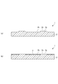
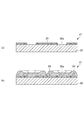
- FIG. 7A shows a photosensitive non-conductive resin on the metal plate 22, and the non-conductive resin corresponding to the conductive portion 22a is removed by exposure and development.
- a method for forming the non-conductive film 23 having a desired pattern has also been proposed.
- FIG. 7B shows a state in which nickel (electric nickel) 24 is electrodeposited on the conductive portion 22a using the cathode plate 21 on which the non-conductive film 23 is formed. Also in the cathode plate 21, the nickel 24 begins to be electrodeposited from the conductive portion 22a and grows not only in the thickness direction but also in the plane direction.
- the non-conductive film (non-conductive part) formed on the cathode plate has a long life, and the non-conductive film is missing (deteriorated). Even in such a case, it is required to be easily maintainable.
- the nonconductive film 23 is formed with a uniform film thickness. can do.
- the nickel 24 is peeled off after electrodeposition, the nickel 24 is caught by the step of the non-conductive film 23 constituting the convex portion, and a large impact is easily applied to the non-conductive film 23. Missing will occur.
- the present invention is a metal electrodeposition cathode that is difficult to remove a non-conductive film on a metal plate, can be used repeatedly, and is easy to maintain even when the non-conductive film is missing. It aims at providing a board and its manufacturing method.
- the inventors of the present invention have made extensive studies to solve the above-mentioned problem. As a result, it has been found that by providing a protrusion on the metal plate as a conductive portion and providing a non-conductive film on the metal surface other than the protrusion, the non-conductive film is not easily lost. Furthermore, by making the shape of the side surface of the projection part a predetermined shape, it is possible to more effectively prevent the loss of the non-conductive film, and even when maintenance by re-forming the non-conductive film is necessary, The present inventors have found that maintenance is facilitated without removing the non-conductive film when the non-conductive film is peeled off, and the present invention has been completed.
- the height L1 of the protrusion 2a is excessive, for example, when a non-conductive film is formed by screen printing, the number of times of application increases and productivity decreases.
- the height L1 is excessively large, distortion of the metal plate 2 is likely to occur during the processing of the protrusion 2a, and the metal plate 2 is likely to warp, making it difficult to form the non-conductive film 3.
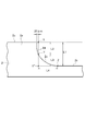
- FIG. 3 is an enlarged cross-sectional view of the main part, in which the A part in FIG. 2 is enlarged, and is an enlarged cross-sectional view of the main part for explaining the side shape of the protrusion of the metal plate.
- the side surface of the protrusion 2a has a shape composed of a substantially vertical portion 2d and an inclined portion 2e.
- the substantially vertical portion 2d is a portion that is formed substantially perpendicular to the upper surface that becomes the conductive portion 2c of the protrusion 2a.
- the inclined portion 2e is a portion formed to be inclined from the substantially vertical portion 2d toward the flat portion 2c.
- the shape of the side surface of the protruding portion 2a is the intersection of the line vertically dropped from the position X 20 ⁇ m away from the outer peripheral edge of the protruding portion 2a and the side surface of the protruding portion 2a.
- the length L2 from X to Y is 40 ⁇ m or more, and preferably 100 ⁇ m or more.
- the outer peripheral edge of the protruding portion 2a is the outer peripheral edge (edge portion) of the upper surface that becomes the conductive portion 2c of the protruding portion 2a.
- the length L2 is 0.8 times (L1 ⁇ 0.8 ⁇ m) or less of the height L1 of the protrusion 2a.
- the length L2 is L1 ⁇ 0.8 ⁇ m or less, the inclined portion 2e can be effectively secured, and as described above, when the nonconductive film 3 is peeled from the metal plate 2, the side surface of the protruding portion 2a In other words, the remaining peeling of the non-conductive film 3 is less likely to occur.
- the non-conductive film 3 is not particularly limited as long as the non-conductive film 3 is non-conductive and is made of a material that is less corroded by the electrolyte used.
- a thermosetting resin or a photo-curing (ultraviolet-curing resin) resin from the viewpoint of easy film formation.
- Specific examples include insulating resins such as epoxy resins, phenol resins, polyamide resins, and polyimide resins.
- a plurality of disc-shaped protrusions 2 a are formed on the surface of the metal plate 2. For example, a portion other than the protrusion 2a is cut away from the flat metal plate 2 to leave the protrusion 2a having the height L1, and the flat portion 2b is formed.
- a processing method wet etching processing or end mill processing is preferable, and wet etching processing is more preferable for processing a large area.
- a photosensitive etching resist is applied to the surface of the stainless steel plate, and then exposed through a film or glass on which a desired pattern is drawn and etched.
- the etching resist is removed by development processing.
- the developed stainless steel plate is attached to an etching solution (for example, ferric chloride solution), a part of the stainless steel plate from which the etching resist is removed is removed, and finally the etching resist is peeled off to obtain a desired
- etching solution for example, ferric chloride solution
- the etching rate of the stainless in the vicinity of the resist is slower than that of the portion away from the resist end, so that the cross-sectional shape of the protrusion 2a is a shape formed by the substantially vertical portion 2d and the inclined portion 2e. Become. Moreover, since a large area can be processed at once, it can be manufactured in a short time.
- the protrusion 2a may be formed only on one surface of the metal plate 2 or may be formed on both surfaces of the metal plate 2.
- the non-conductive film 3 is formed on the flat portion 2b that is the surface of the metal plate 2 other than the protruding portion 2a.
- the method for forming the non-conductive film 3 is not particularly limited, and can be performed by screen printing. In the case where the material of the non-conductive film 3 is a thermosetting resin or a photo-curing resin, heat curing or photo-curing may be performed as necessary.
- a non-conductive film 3 was formed by applying a thermosetting epoxy resin on the flat portion 2b of the metal plate 2 by screen printing and curing it by heating at 150 ° C. for 60 minutes.
- Example 5 A cathode plate 1 was prepared in the same manner as in Example 1 except that a disc-shaped protrusion was formed using a radius end mill drill.
- the height L2 of the substantially vertical portion 2d was measured by a laser displacement meter.
- the average height L3 of the inclined portion 2e was 200 ⁇ m
- the length L4 of the inclined portion 2e was 220 ⁇ m.
- electro nickel was produced by electrolytic treatment. Specifically, a cathode plate and an anode plate made of electric nickel of 200 mm ⁇ 100 mm ⁇ 10 mm were immersed facing each other in an electrolytic cell containing a nickel chloride electrolyte. Then, nickel was electrodeposited on the surface of the cathode plate under the conditions of an initial current density of 710 A / m 2 and an electrolysis time of 3 days. After electrolysis, the electronickel deposited on the cathode plate was peeled off to obtain a small lump of electronickel for plating.
Landscapes
- Chemical & Material Sciences (AREA)
- Metallurgy (AREA)
- Engineering & Computer Science (AREA)
- Materials Engineering (AREA)
- Chemical Kinetics & Catalysis (AREA)
- Organic Chemistry (AREA)
- Electrochemistry (AREA)
- General Chemical & Material Sciences (AREA)
- Mechanical Engineering (AREA)
- Crystallography & Structural Chemistry (AREA)
- Electrolytic Production Of Metals (AREA)
- Milling Processes (AREA)
- ing And Chemical Polishing (AREA)
Priority Applications (3)
| Application Number | Priority Date | Filing Date | Title |
|---|---|---|---|
| EP18809926.1A EP3633074B1 (en) | 2017-05-29 | 2018-03-29 | Cathode plate for metal electrodeposition and manufacturing method for same |
| CN201880026566.8A CN110546310B (zh) | 2017-05-29 | 2018-03-29 | 金属电沉积用的阴极板及其制造方法 |
| CA3064525A CA3064525C (en) | 2017-05-29 | 2018-03-29 | Cathode plate for metal electrodeposition and manufacturing method for same |
Applications Claiming Priority (2)
| Application Number | Priority Date | Filing Date | Title |
|---|---|---|---|
| JP2017105796A JP6500937B2 (ja) | 2017-05-29 | 2017-05-29 | 金属電着用陰極板及びその製造方法 |
| JP2017-105796 | 2017-05-29 |
Publications (1)
| Publication Number | Publication Date |
|---|---|
| WO2018220979A1 true WO2018220979A1 (ja) | 2018-12-06 |
Family
ID=64454726
Family Applications (1)
| Application Number | Title | Priority Date | Filing Date |
|---|---|---|---|
| PCT/JP2018/013187 Ceased WO2018220979A1 (ja) | 2017-05-29 | 2018-03-29 | 金属電着用陰極板及びその製造方法 |
Country Status (5)
| Country | Link |
|---|---|
| EP (1) | EP3633074B1 (enExample) |
| JP (1) | JP6500937B2 (enExample) |
| CN (1) | CN110546310B (enExample) |
| CA (1) | CA3064525C (enExample) |
| WO (1) | WO2018220979A1 (enExample) |
Families Citing this family (6)
| Publication number | Priority date | Publication date | Assignee | Title |
|---|---|---|---|---|
| JP7188216B2 (ja) * | 2019-03-25 | 2022-12-13 | 住友金属鉱山株式会社 | 金属電着用の陰極板の製造方法 |
| JP7238524B2 (ja) * | 2019-03-25 | 2023-03-14 | 住友金属鉱山株式会社 | 金属電着用の陰極板 |
| JP7188217B2 (ja) * | 2019-03-25 | 2022-12-13 | 住友金属鉱山株式会社 | 金属電着用の陰極板の製造方法 |
| JP7188219B2 (ja) * | 2019-03-25 | 2022-12-13 | 住友金属鉱山株式会社 | 金属電着用の陰極板 |
| JP7188218B2 (ja) * | 2019-03-25 | 2022-12-13 | 住友金属鉱山株式会社 | 金属電着用の陰極板 |
| JP2021095594A (ja) * | 2019-12-13 | 2021-06-24 | 住友金属鉱山株式会社 | ボタン型電気ニッケルの製造方法 |
Citations (6)
| Publication number | Priority date | Publication date | Assignee | Title |
|---|---|---|---|---|
| JPS5136693B1 (enExample) | 1971-03-17 | 1976-10-09 | ||
| JPS52152832A (en) | 1976-06-15 | 1977-12-19 | Int Nickel Co | Method of producing ordinary electrolytic nickel or annular nickel product from electroplating bath providing precipitates of large stress |
| JPS5629960B2 (enExample) | 1976-04-01 | 1981-07-11 | ||
| JPH10317197A (ja) * | 1997-05-14 | 1998-12-02 | Sumitomo Metal Mining Co Ltd | メッキ用電気ニッケル、その製造用陰極板及び製造方法 |
| US20110233055A1 (en) * | 2008-09-09 | 2011-09-29 | Steelmore Holdingd Pty Ltd | cathode and a method of forming a cathode |
| JP2015196905A (ja) * | 2014-04-02 | 2015-11-09 | オーシーアイ カンパニー リミテッドOCI Company Ltd. | 電解めっき用電極及びこれを含む電解めっき装置 |
Family Cites Families (3)
| Publication number | Priority date | Publication date | Assignee | Title |
|---|---|---|---|---|
| JPS6038678Y2 (ja) * | 1981-05-15 | 1985-11-19 | 住友金属鉱山株式会社 | 金属電着用母板 |
| WO2002002848A2 (en) * | 2000-06-30 | 2002-01-10 | Honeywell International Inc. | Method and apparatus for processing metals, and the metals so produced |
| EP3187626B1 (en) * | 2014-07-15 | 2020-09-16 | De Nora Permelec Ltd | Electrolysis cathode and method for producing electrolysis cathode |
-
2017
- 2017-05-29 JP JP2017105796A patent/JP6500937B2/ja active Active
-
2018
- 2018-03-29 CN CN201880026566.8A patent/CN110546310B/zh active Active
- 2018-03-29 EP EP18809926.1A patent/EP3633074B1/en active Active
- 2018-03-29 WO PCT/JP2018/013187 patent/WO2018220979A1/ja not_active Ceased
- 2018-03-29 CA CA3064525A patent/CA3064525C/en active Active
Patent Citations (6)
| Publication number | Priority date | Publication date | Assignee | Title |
|---|---|---|---|---|
| JPS5136693B1 (enExample) | 1971-03-17 | 1976-10-09 | ||
| JPS5629960B2 (enExample) | 1976-04-01 | 1981-07-11 | ||
| JPS52152832A (en) | 1976-06-15 | 1977-12-19 | Int Nickel Co | Method of producing ordinary electrolytic nickel or annular nickel product from electroplating bath providing precipitates of large stress |
| JPH10317197A (ja) * | 1997-05-14 | 1998-12-02 | Sumitomo Metal Mining Co Ltd | メッキ用電気ニッケル、その製造用陰極板及び製造方法 |
| US20110233055A1 (en) * | 2008-09-09 | 2011-09-29 | Steelmore Holdingd Pty Ltd | cathode and a method of forming a cathode |
| JP2015196905A (ja) * | 2014-04-02 | 2015-11-09 | オーシーアイ カンパニー リミテッドOCI Company Ltd. | 電解めっき用電極及びこれを含む電解めっき装置 |
Non-Patent Citations (1)
| Title |
|---|
| See also references of EP3633074A4 |
Also Published As
| Publication number | Publication date |
|---|---|
| CN110546310B (zh) | 2020-09-15 |
| JP2018199857A (ja) | 2018-12-20 |
| CA3064525A1 (en) | 2018-12-06 |
| CA3064525C (en) | 2020-03-24 |
| CN110546310A (zh) | 2019-12-06 |
| JP6500937B2 (ja) | 2019-04-17 |
| EP3633074A1 (en) | 2020-04-08 |
| EP3633074B1 (en) | 2022-10-05 |
| EP3633074A4 (en) | 2021-03-10 |
Similar Documents
| Publication | Publication Date | Title |
|---|---|---|
| WO2018220979A1 (ja) | 金属電着用陰極板及びその製造方法 | |
| CN102149855B (zh) | 电铸方法 | |
| WO2018016362A1 (ja) | 金属電着用陰極板及びその製造方法 | |
| NO149896B (no) | Rektangulaer katodeenhet for gjentatt anvendelse | |
| JP2018199857A5 (enExample) | ||
| KR20230033657A (ko) | 금형의 가공방법 | |
| JP6638589B2 (ja) | 金属電着用陰極板及びその製造方法 | |
| US3695927A (en) | Electrodeposition process for producing perforated foils with raised portions at the edges of the holes | |
| JP7188219B2 (ja) | 金属電着用の陰極板 | |
| JP7188218B2 (ja) | 金属電着用の陰極板 | |
| JP7188217B2 (ja) | 金属電着用の陰極板の製造方法 | |
| JP7188216B2 (ja) | 金属電着用の陰極板の製造方法 | |
| JP6737036B2 (ja) | 金属電着用陰極板及びその製造方法 | |
| JP7238524B2 (ja) | 金属電着用の陰極板 | |
| JP6737035B2 (ja) | 金属電着用陰極板及びその製造方法 | |
| JP2019108592A (ja) | ボタン型電気ニッケルの製造用母板、その製造方法、及びそれを用いたボタン型電気ニッケルの製造方法 | |
| JP2024008385A (ja) | 金属電着用の陰極板の製造方法 | |
| JP6825470B2 (ja) | 試験電着用陰極板、及びその製造方法 | |
| JP2001355091A (ja) | 電解銅箔製造装置 | |
| JP6070521B2 (ja) | 特殊形状電着物の製造方法 | |
| JP6760191B2 (ja) | 特殊形状電着物の製造方法 | |
| JP2023172432A (ja) | 特殊形状電着物用母板の製造方法 | |
| KR20180123786A (ko) | 수직성장 전주가공물과 그 제작 방법 | |
| KR20190001261A (ko) | 수직성장 전주가공물과 그 제작 방법 | |
| KR20180086894A (ko) | 수직성장을 유도하는 전주가공물의 가공방법 |
Legal Events
| Date | Code | Title | Description |
|---|---|---|---|
| 121 | Ep: the epo has been informed by wipo that ep was designated in this application |
Ref document number: 18809926 Country of ref document: EP Kind code of ref document: A1 |
|
| ENP | Entry into the national phase |
Ref document number: 3064525 Country of ref document: CA |
|
| NENP | Non-entry into the national phase |
Ref country code: DE |
|
| ENP | Entry into the national phase |
Ref document number: 2018809926 Country of ref document: EP Effective date: 20200102 |