WO2018220979A1 - Cathode plate for metal electrodeposition and manufacturing method for same - Google Patents
Cathode plate for metal electrodeposition and manufacturing method for same Download PDFInfo
- Publication number
- WO2018220979A1 WO2018220979A1 PCT/JP2018/013187 JP2018013187W WO2018220979A1 WO 2018220979 A1 WO2018220979 A1 WO 2018220979A1 JP 2018013187 W JP2018013187 W JP 2018013187W WO 2018220979 A1 WO2018220979 A1 WO 2018220979A1
- Authority
- WO
- WIPO (PCT)
- Prior art keywords
- conductive film
- cathode plate
- metal plate
- plate
- nickel
- Prior art date
Links
Images


Classifications
-
- C—CHEMISTRY; METALLURGY
- C25—ELECTROLYTIC OR ELECTROPHORETIC PROCESSES; APPARATUS THEREFOR
- C25D—PROCESSES FOR THE ELECTROLYTIC OR ELECTROPHORETIC PRODUCTION OF COATINGS; ELECTROFORMING; APPARATUS THEREFOR
- C25D17/00—Constructional parts, or assemblies thereof, of cells for electrolytic coating
- C25D17/16—Apparatus for electrolytic coating of small objects in bulk
-
- C—CHEMISTRY; METALLURGY
- C23—COATING METALLIC MATERIAL; COATING MATERIAL WITH METALLIC MATERIAL; CHEMICAL SURFACE TREATMENT; DIFFUSION TREATMENT OF METALLIC MATERIAL; COATING BY VACUUM EVAPORATION, BY SPUTTERING, BY ION IMPLANTATION OR BY CHEMICAL VAPOUR DEPOSITION, IN GENERAL; INHIBITING CORROSION OF METALLIC MATERIAL OR INCRUSTATION IN GENERAL
- C23F—NON-MECHANICAL REMOVAL OF METALLIC MATERIAL FROM SURFACE; INHIBITING CORROSION OF METALLIC MATERIAL OR INCRUSTATION IN GENERAL; MULTI-STEP PROCESSES FOR SURFACE TREATMENT OF METALLIC MATERIAL INVOLVING AT LEAST ONE PROCESS PROVIDED FOR IN CLASS C23 AND AT LEAST ONE PROCESS COVERED BY SUBCLASS C21D OR C22F OR CLASS C25
- C23F1/00—Etching metallic material by chemical means
- C23F1/02—Local etching
- C23F1/04—Chemical milling
-
- C—CHEMISTRY; METALLURGY
- C25—ELECTROLYTIC OR ELECTROPHORETIC PROCESSES; APPARATUS THEREFOR
- C25C—PROCESSES FOR THE ELECTROLYTIC PRODUCTION, RECOVERY OR REFINING OF METALS; APPARATUS THEREFOR
- C25C1/00—Electrolytic production, recovery or refining of metals by electrolysis of solutions
- C25C1/06—Electrolytic production, recovery or refining of metals by electrolysis of solutions or iron group metals, refractory metals or manganese
- C25C1/08—Electrolytic production, recovery or refining of metals by electrolysis of solutions or iron group metals, refractory metals or manganese of nickel or cobalt
-
- C—CHEMISTRY; METALLURGY
- C25—ELECTROLYTIC OR ELECTROPHORETIC PROCESSES; APPARATUS THEREFOR
- C25C—PROCESSES FOR THE ELECTROLYTIC PRODUCTION, RECOVERY OR REFINING OF METALS; APPARATUS THEREFOR
- C25C7/00—Constructional parts, or assemblies thereof, of cells; Servicing or operating of cells
- C25C7/02—Electrodes; Connections thereof
-
- C—CHEMISTRY; METALLURGY
- C25—ELECTROLYTIC OR ELECTROPHORETIC PROCESSES; APPARATUS THEREFOR
- C25D—PROCESSES FOR THE ELECTROLYTIC OR ELECTROPHORETIC PRODUCTION OF COATINGS; ELECTROFORMING; APPARATUS THEREFOR
- C25D1/00—Electroforming
- C25D1/003—3D structures, e.g. superposed patterned layers
-
- C—CHEMISTRY; METALLURGY
- C25—ELECTROLYTIC OR ELECTROPHORETIC PROCESSES; APPARATUS THEREFOR
- C25D—PROCESSES FOR THE ELECTROLYTIC OR ELECTROPHORETIC PRODUCTION OF COATINGS; ELECTROFORMING; APPARATUS THEREFOR
- C25D1/00—Electroforming
- C25D1/20—Separation of the formed objects from the electrodes with no destruction of said electrodes
-
- C—CHEMISTRY; METALLURGY
- C25—ELECTROLYTIC OR ELECTROPHORETIC PROCESSES; APPARATUS THEREFOR
- C25D—PROCESSES FOR THE ELECTROLYTIC OR ELECTROPHORETIC PRODUCTION OF COATINGS; ELECTROFORMING; APPARATUS THEREFOR
- C25D17/00—Constructional parts, or assemblies thereof, of cells for electrolytic coating
- C25D17/10—Electrodes, e.g. composition, counter electrode
- C25D17/12—Shape or form
Definitions
- FIG. 7A shows a photosensitive non-conductive resin on the metal plate 22, and the non-conductive resin corresponding to the conductive portion 22a is removed by exposure and development.
- a method for forming the non-conductive film 23 having a desired pattern has also been proposed.
- FIG. 7B shows a state in which nickel (electric nickel) 24 is electrodeposited on the conductive portion 22a using the cathode plate 21 on which the non-conductive film 23 is formed. Also in the cathode plate 21, the nickel 24 begins to be electrodeposited from the conductive portion 22a and grows not only in the thickness direction but also in the plane direction.
- the non-conductive film (non-conductive part) formed on the cathode plate has a long life, and the non-conductive film is missing (deteriorated). Even in such a case, it is required to be easily maintainable.
- the nonconductive film 23 is formed with a uniform film thickness. can do.
- the nickel 24 is peeled off after electrodeposition, the nickel 24 is caught by the step of the non-conductive film 23 constituting the convex portion, and a large impact is easily applied to the non-conductive film 23. Missing will occur.
- the present invention is a metal electrodeposition cathode that is difficult to remove a non-conductive film on a metal plate, can be used repeatedly, and is easy to maintain even when the non-conductive film is missing. It aims at providing a board and its manufacturing method.
- the inventors of the present invention have made extensive studies to solve the above-mentioned problem. As a result, it has been found that by providing a protrusion on the metal plate as a conductive portion and providing a non-conductive film on the metal surface other than the protrusion, the non-conductive film is not easily lost. Furthermore, by making the shape of the side surface of the projection part a predetermined shape, it is possible to more effectively prevent the loss of the non-conductive film, and even when maintenance by re-forming the non-conductive film is necessary, The present inventors have found that maintenance is facilitated without removing the non-conductive film when the non-conductive film is peeled off, and the present invention has been completed.
- the height L1 of the protrusion 2a is excessive, for example, when a non-conductive film is formed by screen printing, the number of times of application increases and productivity decreases.
- the height L1 is excessively large, distortion of the metal plate 2 is likely to occur during the processing of the protrusion 2a, and the metal plate 2 is likely to warp, making it difficult to form the non-conductive film 3.
- FIG. 3 is an enlarged cross-sectional view of the main part, in which the A part in FIG. 2 is enlarged, and is an enlarged cross-sectional view of the main part for explaining the side shape of the protrusion of the metal plate.
- the side surface of the protrusion 2a has a shape composed of a substantially vertical portion 2d and an inclined portion 2e.
- the substantially vertical portion 2d is a portion that is formed substantially perpendicular to the upper surface that becomes the conductive portion 2c of the protrusion 2a.
- the inclined portion 2e is a portion formed to be inclined from the substantially vertical portion 2d toward the flat portion 2c.
- the shape of the side surface of the protruding portion 2a is the intersection of the line vertically dropped from the position X 20 ⁇ m away from the outer peripheral edge of the protruding portion 2a and the side surface of the protruding portion 2a.
- the length L2 from X to Y is 40 ⁇ m or more, and preferably 100 ⁇ m or more.
- the outer peripheral edge of the protruding portion 2a is the outer peripheral edge (edge portion) of the upper surface that becomes the conductive portion 2c of the protruding portion 2a.
- the length L2 is 0.8 times (L1 ⁇ 0.8 ⁇ m) or less of the height L1 of the protrusion 2a.
- the length L2 is L1 ⁇ 0.8 ⁇ m or less, the inclined portion 2e can be effectively secured, and as described above, when the nonconductive film 3 is peeled from the metal plate 2, the side surface of the protruding portion 2a In other words, the remaining peeling of the non-conductive film 3 is less likely to occur.
- the non-conductive film 3 is not particularly limited as long as the non-conductive film 3 is non-conductive and is made of a material that is less corroded by the electrolyte used.
- a thermosetting resin or a photo-curing (ultraviolet-curing resin) resin from the viewpoint of easy film formation.
- Specific examples include insulating resins such as epoxy resins, phenol resins, polyamide resins, and polyimide resins.
- a plurality of disc-shaped protrusions 2 a are formed on the surface of the metal plate 2. For example, a portion other than the protrusion 2a is cut away from the flat metal plate 2 to leave the protrusion 2a having the height L1, and the flat portion 2b is formed.
- a processing method wet etching processing or end mill processing is preferable, and wet etching processing is more preferable for processing a large area.
- a photosensitive etching resist is applied to the surface of the stainless steel plate, and then exposed through a film or glass on which a desired pattern is drawn and etched.
- the etching resist is removed by development processing.
- the developed stainless steel plate is attached to an etching solution (for example, ferric chloride solution), a part of the stainless steel plate from which the etching resist is removed is removed, and finally the etching resist is peeled off to obtain a desired
- etching solution for example, ferric chloride solution
- the etching rate of the stainless in the vicinity of the resist is slower than that of the portion away from the resist end, so that the cross-sectional shape of the protrusion 2a is a shape formed by the substantially vertical portion 2d and the inclined portion 2e. Become. Moreover, since a large area can be processed at once, it can be manufactured in a short time.
- the protrusion 2a may be formed only on one surface of the metal plate 2 or may be formed on both surfaces of the metal plate 2.
- the non-conductive film 3 is formed on the flat portion 2b that is the surface of the metal plate 2 other than the protruding portion 2a.
- the method for forming the non-conductive film 3 is not particularly limited, and can be performed by screen printing. In the case where the material of the non-conductive film 3 is a thermosetting resin or a photo-curing resin, heat curing or photo-curing may be performed as necessary.
- a non-conductive film 3 was formed by applying a thermosetting epoxy resin on the flat portion 2b of the metal plate 2 by screen printing and curing it by heating at 150 ° C. for 60 minutes.
- Example 5 A cathode plate 1 was prepared in the same manner as in Example 1 except that a disc-shaped protrusion was formed using a radius end mill drill.
- the height L2 of the substantially vertical portion 2d was measured by a laser displacement meter.
- the average height L3 of the inclined portion 2e was 200 ⁇ m
- the length L4 of the inclined portion 2e was 220 ⁇ m.
- electro nickel was produced by electrolytic treatment. Specifically, a cathode plate and an anode plate made of electric nickel of 200 mm ⁇ 100 mm ⁇ 10 mm were immersed facing each other in an electrolytic cell containing a nickel chloride electrolyte. Then, nickel was electrodeposited on the surface of the cathode plate under the conditions of an initial current density of 710 A / m 2 and an electrolysis time of 3 days. After electrolysis, the electronickel deposited on the cathode plate was peeled off to obtain a small lump of electronickel for plating.
Abstract
Provided are: a cathode plate for metal electrodeposition which makes it less likely to lose a non-conductive film on a metal plate, which can be used repeatedly, and for which maintenance is easy even if a non-conductive film is lost; and a manufacturing method for such cathode plate. This cathode plate 1 includes a metal plate 2 on which a plurality of disk-shaped projections 2a are arranged, and a non-conductive film 3 formed in flat sections 2b which are sections of the metal plate 2 other than the projections 2a. The projections 2a each have a side face that has a shape formed of a substantially vertical section 2d and an inclined section 2e. A height L1 of each projection 2a is 50µm to 1000µm, and when an intersection of the side face of the projection and a vertical line that is vertically lowered from a position X that is 20µm outward from the outer peripheral edge of the projection is defined as Y, then a length L2 from X to Y is at least 40µm but not more than 0.8×L1µm.
Description
本発明は、金属電着用陰極板及びその製造方法に関する。
The present invention relates to a metal electrodeposition cathode plate and a method for producing the same.
従来、ニッケルメッキのアノード原料として供せられる電気ニッケルは、アノード保持具となるチタンバスケット内に入れられ、ニッケルメッキ槽内に吊るされて使用されている。このとき、アノード原料である電気ニッケルとしては、陰極板に電着された板状の電気ニッケルを切断して小片状としたものを使用していた。
Conventionally, electric nickel provided as an anode material for nickel plating has been used in a titanium basket serving as an anode holder and suspended in a nickel plating tank. At this time, as the electric nickel as the anode raw material, a plate-like electric nickel electrodeposited on the cathode plate was cut into small pieces.
しかしながら、小片状の電気ニッケルは、角部が鋭いためチタンバスケットへ投入する際の取り扱いが困難であった。また、その小片状の電気ニッケルは、チタンバスケットに投入後に角部がチタンバスケットの網目に引っ掛っていわゆる棚吊りを起こし、チタンバスケット内での充填状態が変化して、メッキむらの発生要因となることがあった。
However, the small pieces of electro nickel were difficult to handle when throwing them into the titanium basket due to the sharp corners. In addition, when the small pieces of electro nickel are put into the titanium basket, the corners get caught in the mesh of the titanium basket and cause so-called shelf hanging, and the filling state in the titanium basket changes, causing uneven plating. There was sometimes.
そこで、角部の取れた丸みのある小塊状(ボタン状)の電気ニッケルの使用が提案されている。小塊状の電気ニッケルは、例えば、複数の円形状の導電部を等間隔に配列している陰極板を用いて、電解によりその導電部にニッケルを析出させた後、導電部から電着したニッケルを剥ぎ取ることにより製造することができる。このような方法によれば、1枚の陰極板から複数の小塊状の電気ニッケルを効率的に製造することができる。
Therefore, it has been proposed to use small rounded (button-shaped) electric nickel with rounded corners. For example, a small lump of electric nickel is obtained by depositing nickel on the conductive part by electrolysis using a cathode plate in which a plurality of circular conductive parts are arranged at equal intervals, and then electrodepositing from the conductive part. It can be manufactured by stripping off. According to such a method, it is possible to efficiently produce a plurality of small blocks of electro nickel from one cathode plate.
図5は、小塊状の電気ニッケルの製造に用いられる従来の陰極板の一例を示す図である。陰極板11は、平板状の金属板12上に、導電部12aとなる箇所を残して非導電膜13でマスキングが施されており、この陰極板11では、導電部12aが凹部となり、非導電膜13が凸部となっている。このような陰極板11を用いることで、その導電部12aに適度な大きさのニッケルを電着させ、小塊状の電気ニッケルを製造する。
FIG. 5 is a diagram showing an example of a conventional cathode plate used in the production of a small block of nickel. The cathode plate 11 is masked with a non-conductive film 13 on a flat metal plate 12 except for a portion to be a conductive portion 12a. In the cathode plate 11, the conductive portion 12a becomes a concave portion and is non-conductive. The film 13 is a convex portion. By using such a cathode plate 11, nickel having an appropriate size is electrodeposited on the conductive portion 12 a to produce a small lump of electric nickel.
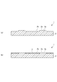
陰極板11のように、金属板12上に非導電膜13を形成する方法としては、例えば、図6(a)に示すように、平板状の金属板12上に、エポキシ樹脂等の熱硬化性の非導電性樹脂をスクリーン印刷法により塗布して加熱することで所望のパターンを有する非導電膜13を形成する方法がある(特許文献1、2参照)。なお、図6(b)は、非導電膜13を形成した陰極板11を用いてニッケル(電気ニッケル)14を導電部12aに電着析出させた状態を示すものである。陰極板11では、ニッケル14が、導電部12aから電着析出しはじめ、厚さ(縦)方向だけではなく平面(横)方向にも成長し、非導電膜13の上部にも盛り上がった状態となる。
As a method of forming the nonconductive film 13 on the metal plate 12 like the cathode plate 11, for example, as shown in FIG. 6A, thermosetting such as epoxy resin on the flat metal plate 12. There is a method of forming a non-conductive film 13 having a desired pattern by applying a conductive non-conductive resin by a screen printing method and heating (see Patent Documents 1 and 2). FIG. 6B shows a state in which nickel (electric nickel) 14 is electrodeposited on the conductive portion 12a using the cathode plate 11 on which the non-conductive film 13 is formed. In the cathode plate 11, nickel 14 begins to be electrodeposited from the conductive portion 12 a, grows not only in the thickness (longitudinal) direction but also in the plane (lateral) direction, and rises above the non-conductive film 13. Become.
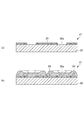
また、例えば図7(a)に示すように、金属板22上に、感光性の非導電性樹脂を塗布し、露光及び現像により導電部22aに相当する箇所の非導電性樹脂を除去して、所望のパターンを有する非導電膜23を形成する方法も提案されている。なお、図7(b)は、非導電膜23を形成した陰極板21を用いてニッケル(電気ニッケル)24を導電部22aに電着析出させた状態を示すものである。陰極板21においても、ニッケル24は、導電部22aから電着析出しはじめ、厚さ方向だけではなく平面方向にも成長していく。
Further, for example, as shown in FIG. 7A, a photosensitive non-conductive resin is applied on the metal plate 22, and the non-conductive resin corresponding to the conductive portion 22a is removed by exposure and development. A method for forming the non-conductive film 23 having a desired pattern has also been proposed. FIG. 7B shows a state in which nickel (electric nickel) 24 is electrodeposited on the conductive portion 22a using the cathode plate 21 on which the non-conductive film 23 is formed. Also in the cathode plate 21, the nickel 24 begins to be electrodeposited from the conductive portion 22a and grows not only in the thickness direction but also in the plane direction.
さらに、導電部となる複数のスタッドが等間隔に複数配列されるように組み込まれた金属の構造体の周囲を射出成形法により絶縁性樹脂で固めることによって、非導電部を構成する陰極板を製造する方法も提案されている(特許文献3参照)。
Further, the cathode plate constituting the non-conductive portion is formed by solidifying the periphery of the metal structure incorporated so that a plurality of studs serving as the conductive portion are arranged at equal intervals with an insulating resin by an injection molding method. A manufacturing method has also been proposed (see Patent Document 3).
さて、上述したような陰極板を用いて小塊状の電気ニッケルの製造する場合、陰極板に形成される非導電膜(非導電部)の寿命が長いこと、その非導電膜が欠落(劣化)した場合でも容易に整備可能であることが要求される。
Now, when manufacturing a small lump of electronickel using the cathode plate as described above, the non-conductive film (non-conductive part) formed on the cathode plate has a long life, and the non-conductive film is missing (deteriorated). Even in such a case, it is required to be easily maintainable.
図6(a)に示したように、金属板12に非導電性樹脂をスクリーン印刷により塗布して非導電膜13を形成した場合、非導電膜13の膜厚は、導電部12aに近づくにしたがって徐々に薄くなるため、導電部12aとの境界で非常に薄くなる。このような非導電膜13の膜厚の変化は、非導電性樹脂の塗布量、非導電性樹脂の粘性及び粘性の温度特性、非導電性樹脂の硬化温度、金属表面の表面粗さや表面自由エネルギー等に依存する。そのため、非導電膜13の膜厚は、導電部12aとの境界で非常に薄くなる。
As shown in FIG. 6A, when the nonconductive film 13 is formed by applying a nonconductive resin to the metal plate 12 by screen printing, the film thickness of the nonconductive film 13 approaches the conductive portion 12a. Therefore, since it becomes thin gradually, it becomes very thin at the boundary with the conductive part 12a. Such a change in the film thickness of the non-conductive film 13 depends on the coating amount of the non-conductive resin, the viscosity and viscosity temperature characteristics of the non-conductive resin, the curing temperature of the non-conductive resin, the surface roughness of the metal surface and the surface freedom. Depends on energy etc. Therefore, the film thickness of the non-conductive film 13 becomes very thin at the boundary with the conductive part 12a.
上述したように、図5、図6に示すような陰極板11を用いて小塊状の電気ニッケルを製造すると、ニッケル14は、導電部12aから電着析出しはじめ、縦方向だけでなく横方向にも成長するため、徐々に非導電膜13の上にも盛り上がった状態となる。そのため、導電部12aとの境界近傍に形成される薄い非導電膜13の部分においては、電解液の浸透により金属板12との密着性が低下しやすくなるとともに、ニッケル14の電着時の応力やその電気ニッケルの剥ぎ取り時の衝撃によって欠落しやすくなる。また、一度、非導電膜13の欠落が発生すると、その周辺の非導電膜13が金属板12の表面から浮き上がるため、その間隙にさらに電解液が侵入しやすくなり、その結果、引き続きニッケルを電着させようとすると、金属板12の表面から浮き上がった非導電膜13の間隙に電解液が潜り込んでニッケル14が電着していく。そして、その間隙に潜り込んで電着したニッケル14を剥ぎ取ろうとすると、ニッケル14が噛み込んでいる非導電膜13をさらに欠落させてしまう。
As described above, when small-sized electronickel is manufactured using the cathode plate 11 as shown in FIGS. 5 and 6, the nickel 14 begins to be electrodeposited from the conductive portion 12a, and not only in the vertical direction but also in the horizontal direction. Therefore, it gradually rises on the non-conductive film 13 as well. Therefore, in the portion of the thin non-conductive film 13 formed in the vicinity of the boundary with the conductive portion 12a, the adhesion with the metal plate 12 is liable to decrease due to the penetration of the electrolytic solution, and the stress during the electrodeposition of the nickel 14 And it tends to be lost due to the impact when stripping the electric nickel. In addition, once the non-conductive film 13 is lost, the surrounding non-conductive film 13 is lifted from the surface of the metal plate 12, so that the electrolyte is more likely to enter the gap. When trying to deposit, the electrolyte sinks into the gap between the non-conductive film 13 floating from the surface of the metal plate 12, and the nickel 14 is electrodeposited. Then, if the nickel 14 that has entered the gap and is electrodeposited is peeled off, the non-conductive film 13 in which the nickel 14 is biting is further lost.
このように、従来の陰極板11においては、連鎖的に非導電膜13の欠落が発生し、欠落部分が広がっていくと隣接する導電部12aから成長したニッケル14同士が連結しやすくなり、所望の形状の電気ニッケルを得ることができず、不良品となる。したがって、非導電膜13の欠落が発生する前に、すべての非導電膜13を剥ぎ取り、再度非導電膜13を形成して陰極板11を整備する必要が生じる。しかしながら、実際には、数回から多くても10回未満程度のニッケルの電着処理を行った段階で陰極板11の整備を行う必要が生じてしまい、生産性が低下するばかりか整備コストも増大する。
Thus, in the conventional cathode plate 11, the non-conductive film 13 is lost in a chain, and the nickel 14 grown from the adjacent conductive parts 12 a is easily connected to each other as the missing part expands. The electric nickel having the shape cannot be obtained, resulting in a defective product. Accordingly, before the non-conductive film 13 is lost, it is necessary to remove all the non-conductive film 13 and form the non-conductive film 13 again to prepare the cathode plate 11. However, in practice, it becomes necessary to maintain the cathode plate 11 at a stage where nickel electrodeposition treatment is performed from several times to at most less than 10 times, which not only reduces productivity but also maintenance costs. Increase.
一方、図7(a)に示したように、感光性の非導電性樹脂を用いて露光及び現像により非導電膜23を形成した陰極板21では、均一な膜厚に非導電膜23を形成することができる。しかしながら、電着後にニッケル24を剥ぎ取る際に、そのニッケル24が凸部を構成する非導電膜23の段差に引っ掛かり、その非導電膜23に大きな衝撃が加わりやすくなるため、やはり非導電膜23の欠落が発生してしまう。
On the other hand, as shown in FIG. 7A, in the cathode plate 21 in which the nonconductive film 23 is formed by exposure and development using a photosensitive nonconductive resin, the nonconductive film 23 is formed with a uniform film thickness. can do. However, when the nickel 24 is peeled off after electrodeposition, the nickel 24 is caught by the step of the non-conductive film 23 constituting the convex portion, and a large impact is easily applied to the non-conductive film 23. Missing will occur.
なお、特許文献3のように射出成形により非導電部を構成する方法では、形成される非導電部の寿命は長くなるものの、陰極板それ自体の製造コストが高くなり、非導電部が劣化した場合の陰極板の整備が困難である。
In addition, in the method of forming the non-conductive portion by injection molding as in Patent Document 3, although the life of the formed non-conductive portion is increased, the manufacturing cost of the cathode plate itself is increased and the non-conductive portion is deteriorated. In this case, maintenance of the cathode plate is difficult.
本発明は、このような従来の事情に鑑み、金属板上の非導電膜が欠落しにくく、繰り返し使用可能で、且つ非導電膜が欠落した場合であっても整備が容易な金属電着用陰極板及びその製造方法を提供することを目的とする。
In view of such conventional circumstances, the present invention is a metal electrodeposition cathode that is difficult to remove a non-conductive film on a metal plate, can be used repeatedly, and is easy to maintain even when the non-conductive film is missing. It aims at providing a board and its manufacturing method.
本発明者らは、上述した解題を解決するために鋭意検討を重ねた。その結果、金属板に突起部を設けて導電部とし、突起部以外の金属表面に非導電膜を設けることで、非導電膜が欠落しにくくなることを見出した。さらに、その突起部の側面の形状を所定の形状にすることにより、非導電膜の欠落をより効果的に防ぐとともに、非導電膜の再形成による整備が必要になった場合であっても、非導電膜を剥ぎ取る際に非導電膜が残存することなく整備が容易となることを見出し、本発明を完成するに至った。
The inventors of the present invention have made extensive studies to solve the above-mentioned problem. As a result, it has been found that by providing a protrusion on the metal plate as a conductive portion and providing a non-conductive film on the metal surface other than the protrusion, the non-conductive film is not easily lost. Furthermore, by making the shape of the side surface of the projection part a predetermined shape, it is possible to more effectively prevent the loss of the non-conductive film, and even when maintenance by re-forming the non-conductive film is necessary, The present inventors have found that maintenance is facilitated without removing the non-conductive film when the non-conductive film is peeled off, and the present invention has been completed.
(1)本発明の第1の発明は、少なくとも一方の表面に複数の円盤状の突起部が配列している金属板と、前記金属板の突起部以外の表面に形成される非導電膜とを有し、前記突起部は、その側面が、略垂直部と傾斜部とからなる形状であり、前記突起部の高さL1は、50μm以上1000μm以下であり、前記突起部の外周縁から外側に20μm離れた位置Xから垂直に下ろした垂線と前記側面との交点をYとするとき、XからYまでの長さL2は40μm以上、0.8×L1μm以下である、金属電着用陰極板である。
(1) The first invention of the present invention is a metal plate in which a plurality of disk-like projections are arranged on at least one surface, and a non-conductive film formed on a surface other than the projections of the metal plate The protrusion has a side surface formed of a substantially vertical portion and an inclined portion, and the height L1 of the protrusion is not less than 50 μm and not more than 1000 μm. The length L2 from X to Y is 40 μm or more and 0.8 × L1 μm or less, where Y is the intersection of a perpendicular line perpendicular to the position X 20 μm away from the side surface and the side surface. It is.
(2)本発明の第2の発明は、第1の発明において、前記金属板は、チタン又はステンレス鋼からなる、金属電着用陰極板である。
(2) According to a second aspect of the present invention, in the first aspect, the metal plate is a metal electrodeposition cathode plate made of titanium or stainless steel.
(3)本発明の第3の発明は、第1又は2の発明において、メッキ用電気ニッケルの製造に使用される、金属電着用陰極板である。
(3) The third invention of the present invention is a metal electrodeposition cathode plate used in the production of electro nickel for plating in the first or second invention.
(4)本発明の第4の発明は、第1乃至第3のいずれかの発明に係る金属電着用陰極板の製造方法であって、金属板の少なくとも一方の表面に、ウェットエッチング加工又はエンドミル加工によって、円盤状の前記突起部を複数形成する、金属電着用陰極板の製造方法である。
(4) A fourth invention of the present invention is a method for manufacturing a metal electrodeposition cathode plate according to any one of the first to third inventions, wherein at least one surface of the metal plate is subjected to wet etching or end milling. It is a manufacturing method of the metal electrodeposition cathode plate which forms the said disk-shaped several projection part by process.
(5)本発明の第5の発明は、第4の発明において、上記エンドミル加工では、ラジアスエンドミルを使用する、金属電着用陰極板の製造方法。
(5) The fifth invention of the present invention is the method for producing a metal electrodeposition cathode plate, wherein in the fourth invention, a radius end mill is used in the end mill processing.
本発明によれば、非導電膜が欠落しにくく、繰り返し使用可能で、且つ非導電膜が欠落した場合であっても容易に整備可能な金属電着用陰極板及びその製造方法を提供することができる。
According to the present invention, it is possible to provide a metal electrodeposition cathode plate and a method for manufacturing the same, which can be easily used even when the non-conductive film is not easily lost, can be repeatedly used, and can be easily maintained. it can.
以下、本発明の金属電着用陰極板を、電気ニッケルの製造に使用される金属電着用陰極板に適用した実施形態(以下、「本実施の形態」という)について詳細に説明する。なお、本発明は、以下の実施形態に限定されるものではなく、本発明の要旨を変更しない範囲で適宜変更することができる。
Hereinafter, an embodiment in which the metal electrodeposition cathode plate of the present invention is applied to a metal electrodeposition cathode plate used in the production of electric nickel (hereinafter referred to as “this embodiment”) will be described in detail. In addition, this invention is not limited to the following embodiment, In the range which does not change the summary of this invention, it can change suitably.
<1.金属電着用陰極板>
(1)陰極板の構成
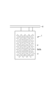
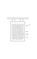
本実施の形態に係る陰極板1は、図1に示すように、複数の円盤状の突起部2aが配列している金属板2と、金属板2の突起部2a以外の表面に形成される非導電膜3とを有する。陰極板1は、後述するように、例えばニッケルを含む電解液や陽極を収容する電解槽内に吊下げ部材5により吊下げられて使用され、その表面に所望とする形状のニッケルを電着析出させる。 <1. Metal electrodeposition cathode plate>
(1) Configuration of Cathode Plate As shown in FIG. 1, thecathode plate 1 according to the present embodiment includes a metal plate 2 in which a plurality of disc-shaped projections 2a are arranged, and a projection 2a of the metal plate 2. And a non-conductive film 3 formed on the surface other than the above. As will be described later, the cathode plate 1 is used by being hung by a hanging member 5 in an electrolytic cell containing, for example, an electrolytic solution containing nickel or an anode, and nickel having a desired shape is electrodeposited on the surface thereof. Let
(1)陰極板の構成
本実施の形態に係る陰極板1は、図1に示すように、複数の円盤状の突起部2aが配列している金属板2と、金属板2の突起部2a以外の表面に形成される非導電膜3とを有する。陰極板1は、後述するように、例えばニッケルを含む電解液や陽極を収容する電解槽内に吊下げ部材5により吊下げられて使用され、その表面に所望とする形状のニッケルを電着析出させる。 <1. Metal electrodeposition cathode plate>
(1) Configuration of Cathode Plate As shown in FIG. 1, the
[金属板]
金属板2は、図1及び図2(a)に示すように、平板状の金属の板であり、複数の円盤状の突起部2aを有する。ここで、金属板2において、突起部2a以外の表面を、突起部2aに対して「平坦部2b」という。また、「突起部の高さL1」は、金属板2における平坦部2bの表面からの突出高さとする。 [Metal plate]
As shown in FIGS. 1 and 2A, themetal plate 2 is a flat metal plate and has a plurality of disc-shaped protrusions 2a. Here, in the metal plate 2, the surface other than the protruding portion 2a is referred to as a “flat portion 2b” with respect to the protruding portion 2a. Further, “the height L1 of the protruding portion” is a protruding height from the surface of the flat portion 2b in the metal plate 2.
金属板2は、図1及び図2(a)に示すように、平板状の金属の板であり、複数の円盤状の突起部2aを有する。ここで、金属板2において、突起部2a以外の表面を、突起部2aに対して「平坦部2b」という。また、「突起部の高さL1」は、金属板2における平坦部2bの表面からの突出高さとする。 [Metal plate]
As shown in FIGS. 1 and 2A, the
なお、図2では、金属板2の一方の面に突起部2aを有する例を示しているが、その両方の面に突起部2aを有していてもよい。
In addition, in FIG. 2, although the example which has the projection part 2a on the one surface of the metal plate 2 is shown, you may have the projection part 2a on the both surfaces.
金属板2の大きさは、特に限定されず、製造する電気ニッケルの所望の大きさや数に応じて適宜設定すればよい。例えば、一辺が100mm以上、2000mm以下の矩形状の大きさとすることができる。また、金属板2の厚みとしては、突起部2aを一方の表面に設ける場合には、例えば、1.5mm以上、5mm以下程度であることが好ましく、突起部2aを両方の表面に設ける場合には、例えば、3mm以上、10mm以下程度であることが好ましい。金属板2の厚みが過小であると、突起部2aと平坦部2bとによって反りが生じやすくなる傾向がある。一方で、金属板2の厚みが過大であると、金属板2の重量が増大して取り扱いが困難になる。
The size of the metal plate 2 is not particularly limited, and may be set as appropriate according to the desired size and number of electric nickel to be manufactured. For example, it can be a rectangular size with one side being 100 mm or more and 2000 mm or less. The thickness of the metal plate 2 is preferably about 1.5 mm or more and 5 mm or less, for example, when the protrusion 2a is provided on one surface, and when the protrusion 2a is provided on both surfaces. Is preferably, for example, about 3 mm or more and 10 mm or less. If the thickness of the metal plate 2 is too small, the protrusions 2a and the flat portions 2b tend to be warped. On the other hand, if the thickness of the metal plate 2 is excessive, the weight of the metal plate 2 increases and handling becomes difficult.
金属板2の材質としては、使用する電解液による腐食が小さく、ニッケル等の電着物とゆるい接着しか形成しない金属であれば特に限定されないが、チタン、ステンレス鋼が好ましく挙げられる。
The material of the metal plate 2 is not particularly limited as long as it is a metal that is less corroded by the electrolyte used and forms only loose adhesion with an electrodeposit such as nickel, but titanium and stainless steel are preferred.
金属板2において、複数の円盤状の突起部2aは、その上面が後述する非導電膜3から露出して導電部としての機能を果たすとともに、非導電膜3が所定の厚みをもって成膜されるべく、隣接する突起部2aによって凹状の段差を形成する。以下、突起部2aのうち、非導電膜3から露出する上面を「導電部2c」ということがある。導電部2cでは、電解処理によりニッケル4を電着析出する。
In the metal plate 2, the plurality of disc-shaped protrusions 2 a are exposed from a non-conductive film 3 described later to function as a conductive part, and the non-conductive film 3 is formed with a predetermined thickness. Accordingly, a concave step is formed by the adjacent protrusion 2a. Hereinafter, the upper surface of the protrusion 2a exposed from the non-conductive film 3 may be referred to as “conductive part 2c”. In the conductive portion 2c, nickel 4 is electrodeposited by electrolytic treatment.
円盤状の突起部2aの大きさは、所望の電気ニッケルの大きさに応じて適宜設定されればよいが、その直径としては、例えば、5mm以上、30mm以下とすることができる。また、突起部2aの高さL1は、50μm以上、1000μm以下であることが好ましく、100μm以上、500μm以下であることがより好ましい。突起部2aの高さL1が過小であると、金属板2の平坦部2b上に形成される非導電膜3の膜厚が不十分となり、ニッケル4の電着時の応力やその電気ニッケルの剥ぎ取り時の衝撃によって欠落しやすくなる。一方、突起部2aの高さL1が過大であると、例えばスクリーン印刷で非導電膜を形成するとき、塗布回数が多くなり生産性が低下する。また、その高さL1が過大であると、突起部2a加工時に金属板2の歪が生じやすくなり、金属板2が反りやすくなるため、非導電膜3の形成が困難になる。なお、金属板2の歪による影響を小さくするため、金属板2の厚みを厚くすることも可能であるが、金属板2の重量が増大し取扱いが困難になる。
The size of the disc-shaped protrusion 2a may be set as appropriate according to the desired size of the electric nickel, and the diameter may be, for example, 5 mm or more and 30 mm or less. In addition, the height L1 of the protrusion 2a is preferably 50 μm or more and 1000 μm or less, and more preferably 100 μm or more and 500 μm or less. If the height L1 of the protrusion 2a is too small, the film thickness of the non-conductive film 3 formed on the flat portion 2b of the metal plate 2 becomes insufficient, and the stress at the time of electrodeposition of the nickel 4 and the electric nickel It tends to be lost due to the impact at the time of peeling. On the other hand, if the height L1 of the protrusion 2a is excessive, for example, when a non-conductive film is formed by screen printing, the number of times of application increases and productivity decreases. On the other hand, if the height L1 is excessively large, distortion of the metal plate 2 is likely to occur during the processing of the protrusion 2a, and the metal plate 2 is likely to warp, making it difficult to form the non-conductive film 3. In addition, in order to reduce the influence by the distortion of the metal plate 2, it is possible to increase the thickness of the metal plate 2, but the weight of the metal plate 2 increases and handling becomes difficult.
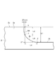
ここで、図3は、図2におけるA部を拡大した要部拡大断面図であり、金属板の突起部の側面形状を説明する要部拡大断面図である。図3に示すように、金属板2において、突起部2aの側面は、略垂直部2dと傾斜部2eとからなる形状を有している。具体的に、略垂直部2dは、突起部2aの導電部2cとなる上面に対して略垂直に形成される箇所である。また、傾斜部2eは、略垂直部2dから平坦部2cに向かって傾斜して形成される箇所である。
Here, FIG. 3 is an enlarged cross-sectional view of the main part, in which the A part in FIG. 2 is enlarged, and is an enlarged cross-sectional view of the main part for explaining the side shape of the protrusion of the metal plate. As shown in FIG. 3, in the metal plate 2, the side surface of the protrusion 2a has a shape composed of a substantially vertical portion 2d and an inclined portion 2e. Specifically, the substantially vertical portion 2d is a portion that is formed substantially perpendicular to the upper surface that becomes the conductive portion 2c of the protrusion 2a. The inclined portion 2e is a portion formed to be inclined from the substantially vertical portion 2d toward the flat portion 2c.
このように、突起部2aの側面が、略垂直部2dと傾斜部2eとからなる形状となるよう構成されることにより、電着処理を繰り返しても非導電膜3の欠落をより効果的に防ぐことができ、繰り返し使用を可能にする。また、非導電膜3の欠落等の劣化により、非導電膜3の再形成による整備が必要となった場合においても、非導電膜3を金属板2から剥離する際、突起部2aの側面に非導電膜3が残存する、いわゆる剥離残りが生じにくく、整備が容易となる。
As described above, the side surface of the protruding portion 2a is configured to have a shape including the substantially vertical portion 2d and the inclined portion 2e, so that the non-conductive film 3 can be more effectively removed even when the electrodeposition process is repeated. It can be prevented and can be used repeatedly. Even when the non-conductive film 3 is deteriorated due to the lack of the non-conductive film 3 and needs to be re-formed, when the non-conductive film 3 is peeled off from the metal plate 2, The non-conductive film 3 remains, so-called peeling residue hardly occurs, and maintenance is easy.
例えば、突起部の側面が、略垂直部のみで形成され、傾斜部が存在しないような形状である場合には、金属板から非導電膜を剥離しようとしても、突起部の側面の略直角に形成される隅に非導電膜が残存しやすくなる。一方で、突起部の側面が、傾斜部のみで形成され、略垂直部が存在しないような形状である場合には、導電部近傍の非導電膜が薄くなり、電着処理により非導電膜が欠落しやすくなる等、非導電膜の劣化が速くなる。
For example, when the side surface of the protrusion is formed only by a substantially vertical portion and does not have an inclined portion, even if an attempt is made to peel the non-conductive film from the metal plate, the side surface of the protrusion is approximately perpendicular to the side surface. The non-conductive film tends to remain in the corner where it is formed. On the other hand, when the side surface of the protruding portion is formed only by the inclined portion and does not have a substantially vertical portion, the non-conductive film near the conductive portion becomes thin, and the non-conductive film is formed by electrodeposition treatment. Deterioration of the non-conductive film is accelerated, such as being easily lost.
より具体的に、突起部2aの側面の形状は、図3に示すように、突起部2aの外周縁から外側に20μm離れた位置Xから垂直に下した線と突起部2aの側面との交点をYとするとき、XからYまでの長さL2は、40μm以上であり、また100μm以上が好ましい。長さL2が40μm以上であることにより、金属板2(平坦部2b)上に形成される非導電膜3が、電解処理を繰り返しても欠落しにくくなる。なお、ここで、突起部2aの外周縁とは、突起部2aの導電部2cとなる上面の外周縁(エッジ部分)である。
More specifically, as shown in FIG. 3, the shape of the side surface of the protruding portion 2a is the intersection of the line vertically dropped from the position X 20 μm away from the outer peripheral edge of the protruding portion 2a and the side surface of the protruding portion 2a. Is Y, the length L2 from X to Y is 40 μm or more, and preferably 100 μm or more. When the length L2 is 40 μm or more, the non-conductive film 3 formed on the metal plate 2 (flat portion 2b) is not easily lost even when the electrolytic treatment is repeated. Here, the outer peripheral edge of the protruding portion 2a is the outer peripheral edge (edge portion) of the upper surface that becomes the conductive portion 2c of the protruding portion 2a.
また、長さL2は、突起部2aの高さL1の0.8倍(L1×0.8μm)以下である。長さL2がL1×0.8μm以下であることにより、傾斜部2eを有効に確保することができ、上述したように、非導電膜3を金属板2から剥離する際に突起部2aの側面に非導電膜3が残存する剥離残りが生じにくくなる。
Also, the length L2 is 0.8 times (L1 × 0.8 μm) or less of the height L1 of the protrusion 2a. When the length L2 is L1 × 0.8 μm or less, the inclined portion 2e can be effectively secured, and as described above, when the nonconductive film 3 is peeled from the metal plate 2, the side surface of the protruding portion 2a In other words, the remaining peeling of the non-conductive film 3 is less likely to occur.
なお、XからYまでの長さL2は、略垂直部2dの高さに相当するが、必ずしも交点Yは、突起部2aの側面の形状を略垂直部2dと傾斜部2eとを明確に分ける分岐点でなくてもよい。以下、長さL2を「略垂直部2dの高さL2」と称する場合がある。
Note that the length L2 from X to Y corresponds to the height of the substantially vertical portion 2d, but the intersection Y does not necessarily separate the shape of the side surface of the protrusion 2a from the substantially vertical portion 2d and the inclined portion 2e. It does not have to be a branch point. Hereinafter, the length L2 may be referred to as “substantially vertical portion 2d height L2”.
また、突起部2aの高さL1と長さL2との差分である長さL3は、10μm以上が好ましく、25μm以上0.7×L1μm以下がより好ましい。以下、長さL3を、「傾斜部2eの高さ」と称する場合がある。さらに、交点Yから垂直に下した線と平坦部2bの表面を水平方向に延長した仮想面との交点をY’とし、突起部2aと平坦部2bとの境界位置をZとし、Y’からZまでの長さをL4としたとき、L3/L4は、0.2以上1以下であることが好ましい。以下、長さL4を「傾斜部2eの長さL4」と称する場合がある。L3/L4は、傾斜部2eの傾斜角度に相当する。
Further, the length L3, which is the difference between the height L1 and the length L2 of the protrusion 2a, is preferably 10 μm or more, and more preferably 25 μm or more and 0.7 × L1 μm or less. Hereinafter, the length L3 may be referred to as “the height of the inclined portion 2e”. Furthermore, the intersection point between the line perpendicular to the intersection point Y and the virtual surface obtained by extending the surface of the flat portion 2b in the horizontal direction is defined as Y ′, the boundary position between the projection portion 2a and the flat portion 2b is defined as Z, and from Y ′ When the length to Z is L4, L3 / L4 is preferably 0.2 or more and 1 or less. Hereinafter, the length L4 may be referred to as “the length L4 of the inclined portion 2e”. L3 / L4 corresponds to the inclination angle of the inclined portion 2e.
長さL3や、L3/L4が上記範囲であることにより、非導電膜3の再形成による整備が必要となった場合においても、非導電膜3を金属板2から剥離する際、突起部2aの側面に非導電膜3が残存する剥離残りが生じにくく、整備が容易である。
When the length L3 and L3 / L4 are in the above ranges, even when the maintenance by re-forming the non-conductive film 3 is necessary, when the non-conductive film 3 is peeled off from the metal plate 2, the protrusion 2a The non-conductive film 3 is hardly left on the side surface of the film, and the maintenance is easy.
また、金属板2の表面、すなわち、金属板2における円盤状の突起部2aの上面には、サンドブラストやエッチングにより細かい凹凸を設けてもよい。これにより、突起部2aに電着したニッケル4が電解処理中に脱落することなく、適度な衝撃で剥ぎ取ることができる。この場合、後述する非導電膜3の膜厚は、金属板2の最大表面粗さRzの2倍以上であることが好ましい。非導電膜3の膜厚が金属板2の最大表面粗さRzの2倍より小さいと、非導電膜3のピンホールや絶縁不良部分の発生が懸念される。
Further, fine irregularities may be provided on the surface of the metal plate 2, that is, on the upper surface of the disc-like protrusion 2a on the metal plate 2 by sandblasting or etching. Thereby, the nickel 4 electrodeposited on the protrusion 2a can be peeled off with an appropriate impact without dropping off during the electrolytic treatment. In this case, the film thickness of the non-conductive film 3 described later is preferably at least twice the maximum surface roughness Rz of the metal plate 2. If the film thickness of the non-conductive film 3 is smaller than twice the maximum surface roughness Rz of the metal plate 2, there is a concern that pinholes and defective insulation portions of the non-conductive film 3 are generated.
[非導電膜]
非導電膜3は、図2に示すように、金属板2における突起部2a以外の表面である平坦部2b上に形成され、これにより、金属板2上に複数配列している突起部2aの上面、すなわち導電部2cが露出された状態となる。そして、このような金属板2の導電部2cにニッケル4が電着析出することにより、そのニッケル4は小塊状の形状に個々に分割されて形成される。 [Non-conductive film]
As shown in FIG. 2, thenon-conductive film 3 is formed on a flat portion 2 b that is a surface other than the protruding portion 2 a in the metal plate 2, whereby a plurality of protruding portions 2 a arranged on the metal plate 2 are formed. The upper surface, that is, the conductive portion 2c is exposed. Then, when nickel 4 is electrodeposited on the conductive portion 2c of the metal plate 2, the nickel 4 is formed by being divided into small blocks.
非導電膜3は、図2に示すように、金属板2における突起部2a以外の表面である平坦部2b上に形成され、これにより、金属板2上に複数配列している突起部2aの上面、すなわち導電部2cが露出された状態となる。そして、このような金属板2の導電部2cにニッケル4が電着析出することにより、そのニッケル4は小塊状の形状に個々に分割されて形成される。 [Non-conductive film]
As shown in FIG. 2, the
非導電膜3は、隣接する突起部2aによって形成された凹状の段差を有する平坦部2b上に形成される。そのため、非導電膜3は、図6に示す従来の非導電膜13のように、端部の膜厚が薄くなりにくく、ニッケル4の電着時の応力や電着後の剥ぎ取り時の衝撃によっても欠落しにくくなる。また、非導電膜3は、図7に示す従来の非導電膜23のように、凸状に突出しておらず、その端部が凹状の段差によって保護されている。よって、ニッケル4を陰極板1から剥ぎ取る際にも、ニッケル4が非導電膜3の端部に与える衝撃は小さく、非導電膜3が欠落しにくい。このように、陰極板1においては、非導電膜3が欠落しにくいことから、非導電膜3を交換することなく、繰り返し電着に使用することが可能であり、整備コストの低減、生産性の向上を図ることが可能である。
The non-conductive film 3 is formed on the flat portion 2b having a concave step formed by the adjacent protrusion 2a. For this reason, the non-conductive film 3 is unlikely to have a thin film thickness at the end, unlike the conventional non-conductive film 13 shown in FIG. It becomes difficult to be lost. Further, unlike the conventional non-conductive film 23 shown in FIG. 7, the non-conductive film 3 does not protrude in a convex shape, and its end is protected by a concave step. Therefore, when the nickel 4 is peeled off from the cathode plate 1, the impact of the nickel 4 on the end portion of the non-conductive film 3 is small and the non-conductive film 3 is not easily lost. Thus, since the non-conductive film 3 is not easily lost in the cathode plate 1, it can be used repeatedly for electrodeposition without replacing the non-conductive film 3, reducing maintenance costs and productivity. It is possible to improve.
なお、スクリーン印刷法によって、金属板2上の平坦部2bに非導電膜3を形成する場合、非導電膜3の材料が突起部2aの上面にも塗布されて導電部2cの表面積が減少し、初期の電流密度が増加することがあるが、電着したニッケル4の特性に不具合が発生しなければ問題ない。また、突起部2aの上面上に付着した非導電膜3は、膜厚が非常に薄いため欠落しやすいが、平坦部2b上に形成される非導電膜3は、膜厚が厚く欠落が抑制されるため問題ない。
When the non-conductive film 3 is formed on the flat portion 2b on the metal plate 2 by screen printing, the material of the non-conductive film 3 is also applied to the upper surface of the protrusion 2a, and the surface area of the conductive portion 2c is reduced. Although the initial current density may increase, there is no problem if there is no problem in the characteristics of the electrodeposited nickel 4. In addition, the non-conductive film 3 attached on the upper surface of the protrusion 2a is very thin and is likely to be lost. However, the non-conductive film 3 formed on the flat portion 2b is thick and suppresses the loss. So no problem.
非導電膜3は、非導電性のものであり、使用する電解液による腐食が小さい材料からなるものであれば特に限定されない。例えば、成膜が容易であるという観点から、熱硬化樹脂又は光硬化(紫外線硬化等)樹脂により構成することが好ましい。具体的には、エポキシ系樹脂、フェノール系樹脂、ポリアミド系樹脂、ポリイミド系樹脂等の絶縁樹脂が挙げられる。
The non-conductive film 3 is not particularly limited as long as the non-conductive film 3 is non-conductive and is made of a material that is less corroded by the electrolyte used. For example, it is preferable to use a thermosetting resin or a photo-curing (ultraviolet-curing resin) resin from the viewpoint of easy film formation. Specific examples include insulating resins such as epoxy resins, phenol resins, polyamide resins, and polyimide resins.
(2)陰極板を用いた電気ニッケルの製造
上述した構成からなる陰極板1では、図2(b)に示すように、非導電膜3から露出する突起部2aの上面が導電部2cとなって、ニッケル4を電着析出させる。陰極板1において、ニッケル4は、厚さ方向だけではなく平面方向にも成長するため、非導電膜3の上部に盛り上がった状態になる。このことから、隣接する突起部2aにおいて導電部2cから成長したニッケル4同士が接触する前に電着を終了することが好ましい。 (2) Manufacture of electric nickel using cathode plate In thecathode plate 1 having the above-described configuration, as shown in FIG. 2B, the upper surface of the protruding portion 2a exposed from the non-conductive film 3 becomes the conductive portion 2c. Then, nickel 4 is electrodeposited. In the cathode plate 1, the nickel 4 grows not only in the thickness direction but also in the planar direction, so that it rises above the non-conductive film 3. For this reason, it is preferable to finish the electrodeposition before the nickels 4 grown from the conductive part 2c come into contact with each other in the adjacent protrusions 2a.
上述した構成からなる陰極板1では、図2(b)に示すように、非導電膜3から露出する突起部2aの上面が導電部2cとなって、ニッケル4を電着析出させる。陰極板1において、ニッケル4は、厚さ方向だけではなく平面方向にも成長するため、非導電膜3の上部に盛り上がった状態になる。このことから、隣接する突起部2aにおいて導電部2cから成長したニッケル4同士が接触する前に電着を終了することが好ましい。 (2) Manufacture of electric nickel using cathode plate In the
そして、ニッケル4の電着が終了した後、陰極板1からそのニッケル4を剥ぎ取ることで、1枚の陰極板1より複数の小塊状の電気ニッケルを得ることができる。上述したように、本実施の形態に係る陰極板1では、非導電膜3が欠落しにくいことから、非導電膜3を交換することなく、繰り返し電着に使用することができ、整備コストの低減、生産性の向上を図ることができる。
Then, after the electrodeposition of the nickel 4 is finished, the nickel 4 is peeled off from the cathode plate 1, whereby a plurality of small blocks of electric nickel can be obtained from one cathode plate 1. As described above, in the cathode plate 1 according to the present embodiment, since the non-conductive film 3 is not easily lost, the non-conductive film 3 can be repeatedly used for electrodeposition without replacement, and maintenance costs are reduced. Reduction and productivity can be improved.
なお、本実施の形態に係る陰極板1は、ニッケル4を電着したが、ニッケルに限定されず、銀、金、亜鉛、錫、クロム、コバルト、又はこれらの合金を電着してもよい。
In addition, although the cathode plate 1 which concerns on this Embodiment electrodeposited nickel 4, it is not limited to nickel, You may electrodeposit silver, gold | metal | money, zinc, tin, chromium, cobalt, or these alloys. .
<2.金属電着用陰極板の製造方法>
本実施の形態に係る陰極板1の製造方法は、図4に示すように、金属板2の少なくとも一方の表面に複数の円盤状の突起部2aを形成する第1工程(図4(a))と、金属板2の突起部2a以外の表面に非導電膜3を形成する第2工程(図4(b))とを有する。 <2. Method for producing metal electrodeposition cathode plate>
As shown in FIG. 4, the manufacturing method of thecathode plate 1 according to the present embodiment is a first step of forming a plurality of disc-shaped protrusions 2a on at least one surface of the metal plate 2 (FIG. 4A). ) And a second step (FIG. 4B) for forming the non-conductive film 3 on the surface of the metal plate 2 other than the protrusions 2a.
本実施の形態に係る陰極板1の製造方法は、図4に示すように、金属板2の少なくとも一方の表面に複数の円盤状の突起部2aを形成する第1工程(図4(a))と、金属板2の突起部2a以外の表面に非導電膜3を形成する第2工程(図4(b))とを有する。 <2. Method for producing metal electrodeposition cathode plate>
As shown in FIG. 4, the manufacturing method of the
[第1工程]
第1工程では、金属板2の表面に、複数の円盤状の突起部2aを形成する。例えば、平板状の金属板2に対して、突起部2a以外の部分を削って、高さL1となる突起部2aを残し、平坦部2bを形成する。加工方法としては、ウェットエッチング加工あるいはエンドミル加工が好ましく、大面積を加工するにはウェットエッチング加工がより好ましい。 [First step]
In the first step, a plurality of disc-shapedprotrusions 2 a are formed on the surface of the metal plate 2. For example, a portion other than the protrusion 2a is cut away from the flat metal plate 2 to leave the protrusion 2a having the height L1, and the flat portion 2b is formed. As a processing method, wet etching processing or end mill processing is preferable, and wet etching processing is more preferable for processing a large area.
第1工程では、金属板2の表面に、複数の円盤状の突起部2aを形成する。例えば、平板状の金属板2に対して、突起部2a以外の部分を削って、高さL1となる突起部2aを残し、平坦部2bを形成する。加工方法としては、ウェットエッチング加工あるいはエンドミル加工が好ましく、大面積を加工するにはウェットエッチング加工がより好ましい。 [First step]
In the first step, a plurality of disc-shaped
例えば、平板状のステンレス鋼板をウェットエッチングで加工する場合には、ステンレス鋼板の表面に感光性のエッチングレジストを塗布し、続いて、所望のパターンを描画したフィルムやガラスを通して露光し、エッチングする部分のエッチングレジストを現像処理により除去する。そして、現像処理されたステンレス鋼板をエッチング液(例えば、塩化第二鉄溶液)に付け、エッチングレジストが除去されたステンレス鋼板の一部を除去し、最後にエッチングレジストを剥離することで、所望のパターンに対応した、複数の円盤状の突起部2aを形成することができる。ウェットエッチングの場合、レジスト近傍部分のステンレスはレジスト端部から離れた部分に比べてエッチング速度が遅くなるため、突起部2aの断面の形状が略垂直部2dと傾斜部2eから形成される形状となる。また、大面積を一度に加工できるため、短時間で製作することができる。
For example, when processing a flat stainless steel plate by wet etching, a photosensitive etching resist is applied to the surface of the stainless steel plate, and then exposed through a film or glass on which a desired pattern is drawn and etched. The etching resist is removed by development processing. Then, the developed stainless steel plate is attached to an etching solution (for example, ferric chloride solution), a part of the stainless steel plate from which the etching resist is removed is removed, and finally the etching resist is peeled off to obtain a desired A plurality of disc-shaped protrusions 2a corresponding to the pattern can be formed. In the case of wet etching, the etching rate of the stainless in the vicinity of the resist is slower than that of the portion away from the resist end, so that the cross-sectional shape of the protrusion 2a is a shape formed by the substantially vertical portion 2d and the inclined portion 2e. Become. Moreover, since a large area can be processed at once, it can be manufactured in a short time.
一方、エンドミル加工の場合は、金属板2にドリルの刃の先端に所望の丸みのある形状のラジアスエンドミルで加工することで、略垂直部2dと傾斜部2eとをより精密に形成することができる。
On the other hand, in the case of end milling, the substantially vertical portion 2d and the inclined portion 2e can be more precisely formed by processing the metal plate 2 with a radius end mill having a desired round shape at the tip of the drill blade. it can.
なお、突起部2aは、金属板2の一方の表面のみに形成してもよいし、金属板2の両方の表面に形成してもよい。
Note that the protrusion 2a may be formed only on one surface of the metal plate 2 or may be formed on both surfaces of the metal plate 2.
[第2工程]
第2工程では、金属板2の突起部2a以外の表面となる平坦部2bに、非導電膜3を形成する。非導電膜3の形成方法としては、特に制限されず、スクリーン印刷により行うことができる。非導電膜3の材料が熱硬化樹脂又は光硬化樹脂である場合には、必要に応じて熱硬化又は光硬化を行えばよい。 [Second step]
In the second step, thenon-conductive film 3 is formed on the flat portion 2b that is the surface of the metal plate 2 other than the protruding portion 2a. The method for forming the non-conductive film 3 is not particularly limited, and can be performed by screen printing. In the case where the material of the non-conductive film 3 is a thermosetting resin or a photo-curing resin, heat curing or photo-curing may be performed as necessary.
第2工程では、金属板2の突起部2a以外の表面となる平坦部2bに、非導電膜3を形成する。非導電膜3の形成方法としては、特に制限されず、スクリーン印刷により行うことができる。非導電膜3の材料が熱硬化樹脂又は光硬化樹脂である場合には、必要に応じて熱硬化又は光硬化を行えばよい。 [Second step]
In the second step, the
本実施の形態に係る陰極板の製造方法によれば、上述した簡易な方法で、金属板2上の非導電膜3が欠落しにくく、繰り返し使用可能な陰極板1を得ることができる。また、非導電膜3の欠落等による劣化により、非導電膜3の再形成による整備が必要になった場合でも、非導電膜3を剥離する際に非導電膜3が突起部2aの側面に残存する剥離残りが生じにくく整備が容易である。
According to the method for manufacturing a cathode plate according to the present embodiment, the non-conductive film 3 on the metal plate 2 is hardly lost and the cathode plate 1 that can be used repeatedly can be obtained by the simple method described above. Even when the non-conductive film 3 is deteriorated due to a lack of the non-conductive film 3 and needs to be re-formed, the non-conductive film 3 is formed on the side surface of the protrusion 2a when the non-conductive film 3 is peeled off. Remaining peeling residue does not easily occur and maintenance is easy.
以下に、本発明の実施例を示してより具体的に説明するが、本発明はこれらの実施例によって何ら限定されるものではない。なお、便宜上、図1乃至図6で示した部材と同一の機能をもつ部材には同一符号を付して説明する。
Hereinafter, the present invention will be described in more detail with reference to examples, but the present invention is not limited to these examples. For convenience, members having the same functions as those shown in FIGS. 1 to 6 will be described with the same reference numerals.
≪陰極板の作製≫
[実施例1]
図1、図2に示すような陰極板1を作製した。具体的には、まず、200mm×100mm×4mmのステンレス鋼製(冷間圧延材)の金属板2に、ウェットエッチングを施し、円盤状の突起部2a(18個)を形成した。このとき、突起部2aの大きさは、直径14mm、高さL1を300μmとし、隣接する突起部2aの最小中心間距離は21mmとした。レーザー変位計で形状を測定したところ略垂直部2dの高さL2は平均120μm、傾斜部2eの高さL3は平均180μm、傾斜部2eの長さL4は平均420μmであった。 ≪Preparation of cathode plate≫
[Example 1]
Acathode plate 1 as shown in FIGS. 1 and 2 was produced. Specifically, first, wet etching was performed on a metal plate 2 made of stainless steel (cold rolled material) of 200 mm × 100 mm × 4 mm to form disk-shaped protrusions 2a (18 pieces). At this time, the size of the protrusion 2a was 14 mm in diameter, the height L1 was 300 μm, and the minimum center-to-center distance between adjacent protrusions 2a was 21 mm. When the shape was measured with a laser displacement meter, the height L2 of the substantially vertical portion 2d was 120 μm on average, the height L3 of the inclined portion 2e was 180 μm on average, and the length L4 of the inclined portion 2e was 420 μm on average.
[実施例1]
図1、図2に示すような陰極板1を作製した。具体的には、まず、200mm×100mm×4mmのステンレス鋼製(冷間圧延材)の金属板2に、ウェットエッチングを施し、円盤状の突起部2a(18個)を形成した。このとき、突起部2aの大きさは、直径14mm、高さL1を300μmとし、隣接する突起部2aの最小中心間距離は21mmとした。レーザー変位計で形状を測定したところ略垂直部2dの高さL2は平均120μm、傾斜部2eの高さL3は平均180μm、傾斜部2eの長さL4は平均420μmであった。 ≪Preparation of cathode plate≫
[Example 1]
A
次に、スクリーン印刷法により、熱硬化性エポキシ樹脂を金属板2における平坦部2b上に塗布し、150℃60分の加熱により硬化させて非導電膜3を形成した。
Next, a non-conductive film 3 was formed by applying a thermosetting epoxy resin on the flat portion 2b of the metal plate 2 by screen printing and curing it by heating at 150 ° C. for 60 minutes.
[実施例2]
金属板2の突起部2aの高さL1を500μmとした以外は、実施例1と同様に、陰極板1を作製した。このようにして作製した陰極板1において、レーザー変位計により、略垂直部2dの高さL2を測定したところ平均で200μm、傾斜部2eの高さL3は平均300μm、傾斜部2eの長さL4は平均650μmであった。 [Example 2]
Acathode plate 1 was produced in the same manner as in Example 1 except that the height L1 of the protrusion 2a of the metal plate 2 was 500 μm. In the cathode plate 1 thus manufactured, the height L2 of the substantially vertical portion 2d was measured by a laser displacement meter. As a result, the average was 200 μm, the height L3 of the inclined portion 2e was 300 μm, and the length L4 of the inclined portion 2e. The average was 650 μm.
金属板2の突起部2aの高さL1を500μmとした以外は、実施例1と同様に、陰極板1を作製した。このようにして作製した陰極板1において、レーザー変位計により、略垂直部2dの高さL2を測定したところ平均で200μm、傾斜部2eの高さL3は平均300μm、傾斜部2eの長さL4は平均650μmであった。 [Example 2]
A
[実施例3]
金属板2の突起部2aの高さL1を60μmとした以外は、実施例1と同様に、陰極板1を作製した。このようにして作製した陰極板1において、レーザー変位計により、略垂直部2dの高さL2を測定したところ平均で45μm、傾斜部2eの高さL3は平均15μm、傾斜部2eの長さL4は平均20μmであった。 [Example 3]
Acathode plate 1 was produced in the same manner as in Example 1 except that the height L1 of the protruding portion 2a of the metal plate 2 was set to 60 μm. In the cathode plate 1 thus manufactured, the height L2 of the substantially vertical portion 2d was measured by a laser displacement meter. As a result, the average was 45 μm, the height L3 of the inclined portion 2e was 15 μm on average, and the length L4 of the inclined portion 2e. The average was 20 μm.
金属板2の突起部2aの高さL1を60μmとした以外は、実施例1と同様に、陰極板1を作製した。このようにして作製した陰極板1において、レーザー変位計により、略垂直部2dの高さL2を測定したところ平均で45μm、傾斜部2eの高さL3は平均15μm、傾斜部2eの長さL4は平均20μmであった。 [Example 3]
A
[実施例4]
金属板2の突起部2aの高さL1を200μmとした以外は、実施例1と同様に、陰極板1を作製した。このようにして作製した陰極板1において、レーザー変位計により、略垂直部2dの高さL2を測定したところ平均で90μm、傾斜部2eの高さL3は平均110μm、傾斜部2eの長さL4は平均240μmであった。 [Example 4]
Acathode plate 1 was produced in the same manner as in Example 1 except that the height L1 of the protruding portion 2a of the metal plate 2 was set to 200 μm. In the cathode plate 1 thus manufactured, the height L2 of the substantially vertical portion 2d was measured by a laser displacement meter. As a result, the average was 90 μm, the height L3 of the inclined portion 2e was 110 μm, and the length L4 of the inclined portion 2e. The average was 240 μm.
金属板2の突起部2aの高さL1を200μmとした以外は、実施例1と同様に、陰極板1を作製した。このようにして作製した陰極板1において、レーザー変位計により、略垂直部2dの高さL2を測定したところ平均で90μm、傾斜部2eの高さL3は平均110μm、傾斜部2eの長さL4は平均240μmであった。 [Example 4]
A
[実施例5]
ラジアスエンドミルドリルを使用して、円盤状の突起部を形成したこと以外は、実施例1と同様に、陰極板1を作製した。このようにして作製した陰極板1において、レーザー変位計により、略垂直部2dの高さL2を測定したところ平均で100μm、傾斜部2eの高さL3は平均200μm、傾斜部2eの長さL4は平均220μmであった。 [Example 5]
Acathode plate 1 was prepared in the same manner as in Example 1 except that a disc-shaped protrusion was formed using a radius end mill drill. In the cathode plate 1 thus manufactured, the height L2 of the substantially vertical portion 2d was measured by a laser displacement meter. As a result, the average height L3 of the inclined portion 2e was 200 μm, and the length L4 of the inclined portion 2e. The average was 220 μm.
ラジアスエンドミルドリルを使用して、円盤状の突起部を形成したこと以外は、実施例1と同様に、陰極板1を作製した。このようにして作製した陰極板1において、レーザー変位計により、略垂直部2dの高さL2を測定したところ平均で100μm、傾斜部2eの高さL3は平均200μm、傾斜部2eの長さL4は平均220μmであった。 [Example 5]
A
[比較例1]
比較例1では、図5、図6に示すような従来の陰極板11を作製した。具体的には、200mm×100mm×4mmのステンレス鋼製(冷間圧延材)の平板状の金属板12に、直径14mmとなる導電部12a(18個)を残して、スクリーン印刷法により、熱硬化性エポキシ樹脂を塗布し、150℃60分の加熱により硬化させて非導電膜13を形成し、陰極板11を作製した。 [Comparative Example 1]
In Comparative Example 1, aconventional cathode plate 11 as shown in FIGS. 5 and 6 was produced. Specifically, a plate-like metal plate 12 made of stainless steel (cold rolled material) of 200 mm × 100 mm × 4 mm is left with a conductive portion 12a (18 pieces) having a diameter of 14 mm, and is heated by screen printing. A curable epoxy resin was applied and cured by heating at 150 ° C. for 60 minutes to form a non-conductive film 13, thereby preparing the cathode plate 11.
比較例1では、図5、図6に示すような従来の陰極板11を作製した。具体的には、200mm×100mm×4mmのステンレス鋼製(冷間圧延材)の平板状の金属板12に、直径14mmとなる導電部12a(18個)を残して、スクリーン印刷法により、熱硬化性エポキシ樹脂を塗布し、150℃60分の加熱により硬化させて非導電膜13を形成し、陰極板11を作製した。 [Comparative Example 1]
In Comparative Example 1, a
[比較例2]
金属板2の突起部2aの高さL1を40μmとした以外は、実施例1と同様に、陰極板1を作製した。このようにして作製した陰極板1において、レーザー変位計により、略垂直部2dの高さL2を測定したところ平均で30μm、傾斜部2eの高さL3は平均10μm、傾斜部2eの長さL4は平均50μmであった。 [Comparative Example 2]
Acathode plate 1 was produced in the same manner as in Example 1 except that the height L1 of the protrusion 2a of the metal plate 2 was 40 μm. In the cathode plate 1 thus manufactured, the height L2 of the substantially vertical portion 2d was measured by a laser displacement meter. As a result, the average was 30 μm, the height L3 of the inclined portion 2e was 10 μm on average, and the length L4 of the inclined portion 2e. The average was 50 μm.
金属板2の突起部2aの高さL1を40μmとした以外は、実施例1と同様に、陰極板1を作製した。このようにして作製した陰極板1において、レーザー変位計により、略垂直部2dの高さL2を測定したところ平均で30μm、傾斜部2eの高さL3は平均10μm、傾斜部2eの長さL4は平均50μmであった。 [Comparative Example 2]
A
[比較例3]
200mm×100mm×4mmのステンレス鋼製(熱間圧延材)の金属板2を使用したこと以外は、実施例4と同様に、陰極板1を作製した。このようにして作製した陰極板1において、レーザー変位計により、略垂直部2dの高さL2を測定したところその一部は20μm程度、傾斜部2eの高さL3は平均180μm、傾斜部2eの長さL4は平均300μmであった。このような略垂直部2dの高さL2が低い箇所は、熱間圧延材の製造工程で形成される表面の凹凸の凹部で形成される。 [Comparative Example 3]
Acathode plate 1 was produced in the same manner as in Example 4 except that a metal plate 2 made of stainless steel (hot rolled material) of 200 mm × 100 mm × 4 mm was used. In the cathode plate 1 thus manufactured, when the height L2 of the substantially vertical portion 2d was measured by a laser displacement meter, a part thereof was about 20 μm, the height L3 of the inclined portion 2e was 180 μm on average, and the height of the inclined portion 2e The length L4 was an average of 300 μm. Such a portion where the height L2 of the substantially vertical portion 2d is low is formed by a concave and convex portion on the surface formed in the manufacturing process of the hot rolled material.
200mm×100mm×4mmのステンレス鋼製(熱間圧延材)の金属板2を使用したこと以外は、実施例4と同様に、陰極板1を作製した。このようにして作製した陰極板1において、レーザー変位計により、略垂直部2dの高さL2を測定したところその一部は20μm程度、傾斜部2eの高さL3は平均180μm、傾斜部2eの長さL4は平均300μmであった。このような略垂直部2dの高さL2が低い箇所は、熱間圧延材の製造工程で形成される表面の凹凸の凹部で形成される。 [Comparative Example 3]
A
[比較例4]
フラットエンドミルドリルを使用して、円盤状の突起部2aを形成したこと以外は、実施例4と同様に、陰極板1を作製した。このようにして作製した陰極板1において、レーザー変位計により、略垂直部2dの高さL2を測定したところ200μmであり、傾斜部はなかった。 [Comparative Example 4]
Acathode plate 1 was produced in the same manner as in Example 4 except that the flat end mill drill was used to form the disc-shaped protrusion 2a. In the cathode plate 1 thus produced, the height L2 of the substantially vertical portion 2d was measured by a laser displacement meter and found to be 200 μm, and there was no inclined portion.
フラットエンドミルドリルを使用して、円盤状の突起部2aを形成したこと以外は、実施例4と同様に、陰極板1を作製した。このようにして作製した陰極板1において、レーザー変位計により、略垂直部2dの高さL2を測定したところ200μmであり、傾斜部はなかった。 [Comparative Example 4]
A
[比較例5]
実施例1と同様に、金属板にウェットエッチングを施し、高さL1が2000μmとなる突起部を形成した。しかしながら、金属板の反りが大きく、スクリーン印刷による非導電膜の形成が困難であった。 [Comparative Example 5]
Similar to Example 1, wet etching was performed on the metal plate to form a protrusion having a height L1 of 2000 μm. However, the warpage of the metal plate is large and it is difficult to form a non-conductive film by screen printing.
≪電気ニッケルの製造≫
各実施例及び比較例にて作製した陰極板を用いて、電解処理により電気ニッケルを製造した。具体的には、塩化ニッケル電解液を収容した電解槽中に、陰極板と、200mm×100mm×10mmの電気ニッケルからなる陽極板とを、対向させて浸漬した。そして、初期電流密度710A/m2、電解時間3日間の条件で、陰極板の表面にニッケルを電着させた。電解後、陰極板上に析出した電気ニッケルを剥ぎ取り、小塊状のメッキ用電気ニッケルを得た。 ≪Manufacture of electric nickel≫
Using the cathode plate produced in each example and comparative example, electro nickel was produced by electrolytic treatment. Specifically, a cathode plate and an anode plate made of electric nickel of 200 mm × 100 mm × 10 mm were immersed facing each other in an electrolytic cell containing a nickel chloride electrolyte. Then, nickel was electrodeposited on the surface of the cathode plate under the conditions of an initial current density of 710 A / m 2 and an electrolysis time of 3 days. After electrolysis, the electronickel deposited on the cathode plate was peeled off to obtain a small lump of electronickel for plating.
≪評価≫
電解処理に使用した陰極板を、そのまま繰り返し利用できる回数を評価した。非導電膜の欠落が広がると、隣接する突起部、導電部で電着したニッケル同士が連結し、所望の形状の電気ニッケルを得られないことがある。したがって、非導電膜が突起部との境界から平坦部方向に1mm以上に亘って欠落した場合には、使用を中止し、その時点までの繰り返し回数を評価した。また、ニッケルの電着と剥ぎ取りは、最大20回まで繰り返した。また、非導電膜が欠落し、導電部の径が1mm以上拡大した場合にも、使用を中止し、この時点までの繰り返し回数を評価した。 ≪Evaluation≫
The number of times that the cathode plate used for the electrolytic treatment can be repeatedly used as it was was evaluated. When the lack of the non-conductive film spreads, the nickel which is electrodeposited at the adjacent protrusions and conductive parts may be connected to each other, so that the desired form of electric nickel may not be obtained. Therefore, when the non-conductive film was missing over 1 mm from the boundary with the protrusion in the flat part direction, the use was stopped and the number of repetitions up to that point was evaluated. The electrodeposition and stripping of nickel were repeated up to 20 times. Also, when the non-conductive film was missing and the diameter of the conductive part expanded by 1 mm or more, the use was stopped and the number of repetitions up to this point was evaluated.
繰り返し回数を評価した陰極板の非導電膜をウォータージェットにより剥離し、非導電膜の剥離性を評価した。具体的には、ウォータージェットを用いて、孔径0.4mm、孔数3個の回転式ノズルを用いて、水圧200MPa、水量10L/分、有効幅30mmで、ノズルを2m/分で移動させながら非導電膜の剥離を実施した。非導電膜の剥離性に関して、陰極板1枚当たり(200mm×100mm)を約20秒以内で非導電膜をほぼ完全に除去できた場合を「良好」とし、20秒以上かかっても非導電膜を除去できなかった場合を「剥離残り発生」として評価した。
The non-conductive film of the cathode plate evaluated for the number of repetitions was peeled off with a water jet, and the peelability of the non-conductive film was evaluated. Specifically, using a water jet, using a rotary nozzle with a hole diameter of 0.4 mm and three holes, the water pressure is 200 MPa, the amount of water is 10 L / min, the effective width is 30 mm, and the nozzle is moved at 2 m / min. The nonconductive film was peeled off. Regarding the peelability of the non-conductive film, the case where the non-conductive film can be almost completely removed within about 20 seconds (200 mm × 100 mm) per cathode plate is defined as “good”. The case where the film could not be removed was evaluated as “remaining peeling”.
表1に、陰極板の構成とともに評価結果を示す。
Table 1 shows the evaluation results together with the configuration of the cathode plate.

表1に示すように、金属板2の平坦部2bに非導電膜3が形成され、突起部2aの高さL1が60μm以上500μm以下である陰極板1を用いた実施例1~5では、非導電膜3の欠落が抑制され、十分に繰り返し使用することができた。特に、突起部2aの高さL1が100μm以上となる実施例1、2、4、5では、繰り返し使用回数が20回を超えていた。また、略垂直部2dの高さL2が40μm以上、0.8×L1μm以下である実施例1~5では、ウォータージェットで非導電膜3を剥離した際に、剥離残り等が発生せず、良好に剥離することができた。
As shown in Table 1, in Examples 1 to 5 using the cathode plate 1 in which the non-conductive film 3 is formed on the flat portion 2b of the metal plate 2 and the height L1 of the protruding portion 2a is 60 μm or more and 500 μm or less, Missing of the non-conductive film 3 was suppressed, and it was possible to use it sufficiently repeatedly. In particular, in Examples 1, 2, 4, and 5 in which the height L1 of the protrusion 2a was 100 μm or more, the number of repeated uses exceeded 20 times. Further, in Examples 1 to 5 in which the height L2 of the substantially vertical portion 2d is 40 μm or more and 0.8 × L1 μm or less, when the non-conductive film 3 is peeled off by the water jet, no peeling residue or the like occurs. It was able to peel well.
一方、平板状の金属板12に非導電膜13が形成された比較例1では、非導電膜14が欠落してしまい、十分に繰り返し使用することができなかった。また、突起部2aの高さL1が低かった比較例2でも非導電膜3が欠落してしまい、十分に繰り返し使用することができなかった。また、比較例3では、突起部2aの側面の形状において略垂直部2dの高さL2が20μmと低い部分から非導電膜3が欠落してしまい、十分に繰り返し使用することができなかった。比較例4では、突起部2aの側面の形状に傾斜部がないため、ウォータージェットで非導電膜3を剥離した際に、突起部2aの側面の略直角に形成された隅に剥離残りが発生した。さらに、比較例5では、突起部2aの高さL1が高すぎため、金属板2の反りが大きくなり、非導電膜の塗布が困難となり、陰極板を構成することができなかった。
On the other hand, in Comparative Example 1 in which the non-conductive film 13 was formed on the flat metal plate 12, the non-conductive film 14 was missing and could not be used sufficiently repeatedly. Further, even in Comparative Example 2 in which the height L1 of the projecting portion 2a was low, the non-conductive film 3 was missing and could not be used repeatedly enough. Further, in Comparative Example 3, the non-conductive film 3 was missing from a portion where the height L2 of the substantially vertical portion 2d was as low as 20 μm in the shape of the side surface of the protruding portion 2a, and could not be used repeatedly enough. In Comparative Example 4, there is no inclined portion in the shape of the side surface of the protruding portion 2a. Therefore, when the non-conductive film 3 is peeled off with a water jet, a peeling residue occurs at a corner formed substantially at right angles to the side surface of the protruding portion 2a. did. Furthermore, in Comparative Example 5, since the height L1 of the protruding portion 2a was too high, the warpage of the metal plate 2 was increased, and it was difficult to apply the non-conductive film, and the cathode plate could not be configured.
1 陰極板
2 金属板
2a 突起部
2b 平坦部
2c 導電部
2d 略垂直部
2e 傾斜部
3 非導電膜
4 ニッケル DESCRIPTION OFSYMBOLS 1 Cathode plate 2 Metal plate 2a Protrusion part 2b Flat part 2c Conductive part 2d Substantially vertical part 2e Inclined part 3 Non-conductive film 4 Nickel
2 金属板
2a 突起部
2b 平坦部
2c 導電部
2d 略垂直部
2e 傾斜部
3 非導電膜
4 ニッケル DESCRIPTION OF
Claims (5)
- 少なくとも一方の表面に複数の円盤状の突起部が配列している金属板と、
前記金属板の突起部以外の表面に形成される非導電膜と、を有し、
前記突起部は、その側面が、略垂直部と傾斜部とからなる形状であり、
前記突起部の高さL1は、50μm以上1000μm以下であり、
前記突起部の外周縁から外側に20μm離れた位置Xから垂直に下ろした垂線と前記側面との交点をYとするとき、XからYまでの長さL2は40μm以上、0.8×L1μm以下である、金属電着用陰極板。 A metal plate in which a plurality of disc-shaped protrusions are arranged on at least one surface;
A non-conductive film formed on the surface other than the protrusions of the metal plate,
The projecting portion has a side surface formed of a substantially vertical portion and an inclined portion,
The height L1 of the protrusion is 50 μm or more and 1000 μm or less,
The length L2 from X to Y is 40 μm or more and 0.8 × L1 μm or less, where Y is the intersection of the perpendicular line drawn from a position X 20 μm away from the outer peripheral edge of the projection and perpendicular to the side surface. A cathode plate for metal electrodeposition. - 前記金属板は、チタン又はステンレス鋼からなる、
請求項1に記載の金属電着用陰極板。 The metal plate is made of titanium or stainless steel.
The cathode plate for metal electrodeposition according to claim 1. - メッキ用電気ニッケルの製造に使用される、
請求項1又は2に記載の金属電着用陰極板。 Used in the production of electro nickel for plating,
The cathode plate for metal electrodeposition according to claim 1 or 2. - 請求項1乃至3のいずれかに記載の金属電着用陰極板の製造方法であって、
金属板の少なくとも一方の表面に、ウェットエッチング加工又はエンドミル加工によって、円盤状の前記突起部を複数形成する、金属電着用陰極板の製造方法。 It is a manufacturing method of the metal electrodeposition cathode plate in any one of Claims 1 thru | or 3, Comprising:
A method for producing a metal electrodeposition cathode plate, wherein a plurality of disk-shaped protrusions are formed on at least one surface of a metal plate by wet etching or end milling. - 上記エンドミル加工では、ラジアスエンドミルを使用する、
請求項4に記載の金属電着用陰極板の製造方法。 In the above end mill processing, a radius end mill is used.
The manufacturing method of the metal electrodeposition cathode plate of Claim 4.
Priority Applications (3)
| Application Number | Priority Date | Filing Date | Title |
|---|---|---|---|
| CA3064525A CA3064525C (en) | 2017-05-29 | 2018-03-29 | Cathode plate for metal electrodeposition and manufacturing method for same |
| CN201880026566.8A CN110546310B (en) | 2017-05-29 | 2018-03-29 | Cathode plate for metal electrodeposition and method for manufacturing the same |
| EP18809926.1A EP3633074B1 (en) | 2017-05-29 | 2018-03-29 | Cathode plate for metal electrodeposition and manufacturing method for same |
Applications Claiming Priority (2)
| Application Number | Priority Date | Filing Date | Title |
|---|---|---|---|
| JP2017105796A JP6500937B2 (en) | 2017-05-29 | 2017-05-29 | Negative electrode plate for metal electrodeposition and method of manufacturing the same |
| JP2017-105796 | 2017-05-29 |
Publications (1)
| Publication Number | Publication Date |
|---|---|
| WO2018220979A1 true WO2018220979A1 (en) | 2018-12-06 |
Family
ID=64454726
Family Applications (1)
| Application Number | Title | Priority Date | Filing Date |
|---|---|---|---|
| PCT/JP2018/013187 WO2018220979A1 (en) | 2017-05-29 | 2018-03-29 | Cathode plate for metal electrodeposition and manufacturing method for same |
Country Status (5)
| Country | Link |
|---|---|
| EP (1) | EP3633074B1 (en) |
| JP (1) | JP6500937B2 (en) |
| CN (1) | CN110546310B (en) |
| CA (1) | CA3064525C (en) |
| WO (1) | WO2018220979A1 (en) |
Families Citing this family (5)
| Publication number | Priority date | Publication date | Assignee | Title |
|---|---|---|---|---|
| JP7188217B2 (en) * | 2019-03-25 | 2022-12-13 | 住友金属鉱山株式会社 | Manufacturing method of cathode plate for metal electrodeposition |
| JP7188219B2 (en) * | 2019-03-25 | 2022-12-13 | 住友金属鉱山株式会社 | Cathode plate for metal electrodeposition |
| JP7188216B2 (en) * | 2019-03-25 | 2022-12-13 | 住友金属鉱山株式会社 | Manufacturing method of cathode plate for metal electrodeposition |
| JP7238524B2 (en) * | 2019-03-25 | 2023-03-14 | 住友金属鉱山株式会社 | Cathode plate for metal electrodeposition |
| JP7188218B2 (en) * | 2019-03-25 | 2022-12-13 | 住友金属鉱山株式会社 | Cathode plate for metal electrodeposition |
Citations (6)
| Publication number | Priority date | Publication date | Assignee | Title |
|---|---|---|---|---|
| JPS5136693B1 (en) | 1971-03-17 | 1976-10-09 | ||
| JPS52152832A (en) | 1976-06-15 | 1977-12-19 | Int Nickel Co | Method of producing ordinary electrolytic nickel or annular nickel product from electroplating bath providing precipitates of large stress |
| JPS5629960B2 (en) | 1976-04-01 | 1981-07-11 | ||
| JPH10317197A (en) * | 1997-05-14 | 1998-12-02 | Sumitomo Metal Mining Co Ltd | Electric nickel for plating, cathode plate for for its production and production |
| US20110233055A1 (en) * | 2008-09-09 | 2011-09-29 | Steelmore Holdingd Pty Ltd | cathode and a method of forming a cathode |
| JP2015196905A (en) * | 2014-04-02 | 2015-11-09 | オーシーアイ カンパニー リミテッドOCI Company Ltd. | Electrode for electrolytic plating and electrolytic plating apparatus |
Family Cites Families (3)
| Publication number | Priority date | Publication date | Assignee | Title |
|---|---|---|---|---|
| JPS6038678Y2 (en) * | 1981-05-15 | 1985-11-19 | 住友金属鉱山株式会社 | Mother plate for metal electrodeposition |
| WO2002002848A2 (en) * | 2000-06-30 | 2002-01-10 | Honeywell International Inc. | Method and apparatus for processing metals, and the metals so produced |
| WO2016010045A1 (en) * | 2014-07-15 | 2016-01-21 | ペルメレック電極株式会社 | Electrolysis cathode and method for producing electrolysis cathode |
-
2017
- 2017-05-29 JP JP2017105796A patent/JP6500937B2/en active Active
-
2018
- 2018-03-29 WO PCT/JP2018/013187 patent/WO2018220979A1/en unknown
- 2018-03-29 CA CA3064525A patent/CA3064525C/en active Active
- 2018-03-29 EP EP18809926.1A patent/EP3633074B1/en active Active
- 2018-03-29 CN CN201880026566.8A patent/CN110546310B/en active Active
Patent Citations (6)
| Publication number | Priority date | Publication date | Assignee | Title |
|---|---|---|---|---|
| JPS5136693B1 (en) | 1971-03-17 | 1976-10-09 | ||
| JPS5629960B2 (en) | 1976-04-01 | 1981-07-11 | ||
| JPS52152832A (en) | 1976-06-15 | 1977-12-19 | Int Nickel Co | Method of producing ordinary electrolytic nickel or annular nickel product from electroplating bath providing precipitates of large stress |
| JPH10317197A (en) * | 1997-05-14 | 1998-12-02 | Sumitomo Metal Mining Co Ltd | Electric nickel for plating, cathode plate for for its production and production |
| US20110233055A1 (en) * | 2008-09-09 | 2011-09-29 | Steelmore Holdingd Pty Ltd | cathode and a method of forming a cathode |
| JP2015196905A (en) * | 2014-04-02 | 2015-11-09 | オーシーアイ カンパニー リミテッドOCI Company Ltd. | Electrode for electrolytic plating and electrolytic plating apparatus |
Non-Patent Citations (1)
| Title |
|---|
| See also references of EP3633074A4 |
Also Published As
| Publication number | Publication date |
|---|---|
| EP3633074A4 (en) | 2021-03-10 |
| EP3633074A1 (en) | 2020-04-08 |
| EP3633074B1 (en) | 2022-10-05 |
| CA3064525A1 (en) | 2018-12-06 |
| CN110546310A (en) | 2019-12-06 |
| CN110546310B (en) | 2020-09-15 |
| JP2018199857A (en) | 2018-12-20 |
| JP6500937B2 (en) | 2019-04-17 |
| CA3064525C (en) | 2020-03-24 |
Similar Documents
| Publication | Publication Date | Title |
|---|---|---|
| WO2018220979A1 (en) | Cathode plate for metal electrodeposition and manufacturing method for same | |
| WO2018016362A1 (en) | Metal electrodeposition cathode plate and production method therefor | |
| CN102149855B (en) | Electroforming method | |
| JP6638589B2 (en) | Cathode plate for metal electrodeposition and method for producing the same | |
| NO149896B (en) | RECTANGULAR REPEATED USE UNITS OF CATODE | |
| JP2018199857A5 (en) | ||
| US3695927A (en) | Electrodeposition process for producing perforated foils with raised portions at the edges of the holes | |
| JP7188219B2 (en) | Cathode plate for metal electrodeposition | |
| JP7188218B2 (en) | Cathode plate for metal electrodeposition | |
| JP7188217B2 (en) | Manufacturing method of cathode plate for metal electrodeposition | |
| JP7188216B2 (en) | Manufacturing method of cathode plate for metal electrodeposition | |
| JP7238524B2 (en) | Cathode plate for metal electrodeposition | |
| KR20180089068A (en) | Method and workpiece of electroforming. | |
| JP6737036B2 (en) | Metal electrodeposited cathode plate and method for producing the same | |
| JP6737035B2 (en) | Metal electrodeposited cathode plate and method for producing the same | |
| JP2024008385A (en) | Method of producing cathode plate for use in electrodepositing metal | |
| JP2001355091A (en) | Electrolytic copper foil manufacturing device | |
| JP6070521B2 (en) | Manufacturing method of special shape electrodeposits | |
| JP6760191B2 (en) | Manufacturing method of specially shaped electrodeposition | |
| JPH10317197A (en) | Electric nickel for plating, cathode plate for for its production and production | |
| JP6825470B2 (en) | Test power wearing cathode plate and its manufacturing method | |
| JP2019108592A (en) | Button-type electrolytic nickel mother board for production and production method thereof, and button-type electrolytic nickel production method using the same | |
| KR20180123786A (en) | Method of inducing vertical groth in electroforming | |
| JPH04221090A (en) | Production of starting sheet for nickel electrolysis | |
| KR20060054858A (en) | Method for manufacturing the thin film by electro-forming |
Legal Events
| Date | Code | Title | Description |
|---|---|---|---|
| 121 | Ep: the epo has been informed by wipo that ep was designated in this application |
Ref document number: 18809926 Country of ref document: EP Kind code of ref document: A1 |
|
| ENP | Entry into the national phase |
Ref document number: 3064525 Country of ref document: CA |
|
| NENP | Non-entry into the national phase |
Ref country code: DE |
|
| ENP | Entry into the national phase |
Ref document number: 2018809926 Country of ref document: EP Effective date: 20200102 |