WO2018220901A1 - セラミック電子部品の製造方法及びセラミック電子部品 - Google Patents
セラミック電子部品の製造方法及びセラミック電子部品 Download PDFInfo
- Publication number
- WO2018220901A1 WO2018220901A1 PCT/JP2018/003751 JP2018003751W WO2018220901A1 WO 2018220901 A1 WO2018220901 A1 WO 2018220901A1 JP 2018003751 W JP2018003751 W JP 2018003751W WO 2018220901 A1 WO2018220901 A1 WO 2018220901A1
- Authority
- WO
- WIPO (PCT)
- Prior art keywords
- electronic component
- ceramic electronic
- low resistance
- ceramic
- metal oxide
- Prior art date
- Legal status (The legal status is an assumption and is not a legal conclusion. Google has not performed a legal analysis and makes no representation as to the accuracy of the status listed.)
- Ceased
Links
Images

Classifications
-
- C—CHEMISTRY; METALLURGY
- C25—ELECTROLYTIC OR ELECTROPHORETIC PROCESSES; APPARATUS THEREFOR
- C25D—PROCESSES FOR THE ELECTROLYTIC OR ELECTROPHORETIC PRODUCTION OF COATINGS; ELECTROFORMING; APPARATUS THEREFOR
- C25D5/00—Electroplating characterised by the process; Pretreatment or after-treatment of workpieces
- C25D5/02—Electroplating of selected surface areas
- C25D5/024—Electroplating of selected surface areas using locally applied electromagnetic radiation, e.g. lasers
-
- H—ELECTRICITY
- H01—ELECTRIC ELEMENTS
- H01G—CAPACITORS; CAPACITORS, RECTIFIERS, DETECTORS, SWITCHING DEVICES, LIGHT-SENSITIVE OR TEMPERATURE-SENSITIVE DEVICES OF THE ELECTROLYTIC TYPE
- H01G4/00—Fixed capacitors; Processes of their manufacture
- H01G4/002—Details
- H01G4/228—Terminals
- H01G4/232—Terminals electrically connecting two or more layers of a stacked or rolled capacitor
-
- C—CHEMISTRY; METALLURGY
- C25—ELECTROLYTIC OR ELECTROPHORETIC PROCESSES; APPARATUS THEREFOR
- C25D—PROCESSES FOR THE ELECTROLYTIC OR ELECTROPHORETIC PRODUCTION OF COATINGS; ELECTROFORMING; APPARATUS THEREFOR
- C25D5/00—Electroplating characterised by the process; Pretreatment or after-treatment of workpieces
- C25D5/10—Electroplating with more than one layer of the same or of different metals
-
- C—CHEMISTRY; METALLURGY
- C25—ELECTROLYTIC OR ELECTROPHORETIC PROCESSES; APPARATUS THEREFOR
- C25D—PROCESSES FOR THE ELECTROLYTIC OR ELECTROPHORETIC PRODUCTION OF COATINGS; ELECTROFORMING; APPARATUS THEREFOR
- C25D5/00—Electroplating characterised by the process; Pretreatment or after-treatment of workpieces
- C25D5/54—Electroplating of non-metallic surfaces
-
- C—CHEMISTRY; METALLURGY
- C25—ELECTROLYTIC OR ELECTROPHORETIC PROCESSES; APPARATUS THEREFOR
- C25D—PROCESSES FOR THE ELECTROLYTIC OR ELECTROPHORETIC PRODUCTION OF COATINGS; ELECTROFORMING; APPARATUS THEREFOR
- C25D7/00—Electroplating characterised by the article coated
- C25D7/12—Semiconductors
-
- H—ELECTRICITY
- H01—ELECTRIC ELEMENTS
- H01G—CAPACITORS; CAPACITORS, RECTIFIERS, DETECTORS, SWITCHING DEVICES, LIGHT-SENSITIVE OR TEMPERATURE-SENSITIVE DEVICES OF THE ELECTROLYTIC TYPE
- H01G4/00—Fixed capacitors; Processes of their manufacture
- H01G4/002—Details
- H01G4/018—Dielectrics
- H01G4/06—Solid dielectrics
- H01G4/08—Inorganic dielectrics
- H01G4/12—Ceramic dielectrics
- H01G4/1209—Ceramic dielectrics characterised by the ceramic dielectric material
- H01G4/1218—Ceramic dielectrics characterised by the ceramic dielectric material based on titanium oxides or titanates
- H01G4/1227—Ceramic dielectrics characterised by the ceramic dielectric material based on titanium oxides or titanates based on alkaline earth titanates
-
- H—ELECTRICITY
- H01—ELECTRIC ELEMENTS
- H01G—CAPACITORS; CAPACITORS, RECTIFIERS, DETECTORS, SWITCHING DEVICES, LIGHT-SENSITIVE OR TEMPERATURE-SENSITIVE DEVICES OF THE ELECTROLYTIC TYPE
- H01G4/00—Fixed capacitors; Processes of their manufacture
- H01G4/30—Stacked capacitors
-
- H—ELECTRICITY
- H01—ELECTRIC ELEMENTS
- H01G—CAPACITORS; CAPACITORS, RECTIFIERS, DETECTORS, SWITCHING DEVICES, LIGHT-SENSITIVE OR TEMPERATURE-SENSITIVE DEVICES OF THE ELECTROLYTIC TYPE
- H01G4/00—Fixed capacitors; Processes of their manufacture
- H01G4/002—Details
- H01G4/228—Terminals
- H01G4/232—Terminals electrically connecting two or more layers of a stacked or rolled capacitor
- H01G4/2325—Terminals electrically connecting two or more layers of a stacked or rolled capacitor characterised by the material of the terminals
Definitions
- the present invention relates to a method for manufacturing a ceramic electronic component, and more particularly to a method for forming a plating electrode on the surface of a ceramic body and a ceramic electronic component.
- a method for forming an external electrode of an electronic component has been to apply an electrode paste to both end faces of a ceramic body, and then form a base electrode by baking or thermosetting the electrode paste, and then forming the base electrode on the base electrode.
- a plating electrode is formed by plating.
- the electrode paste is applied by a method of immersing the end of the electronic component in a paste film formed with a predetermined thickness, or a method using transfer using a roller or the like. In these techniques, there is a problem that the thickness of the electrode increases due to the application of the electrode paste, and the outer dimensions increase accordingly.
- an electrode forming method using such an electrode paste a plurality of ends of the internal electrode are exposed close to the end face of the ceramic body, and dummy terminals called anchor tabs are connected to the end of the internal electrode.
- Proposed a method to form an external electrode by exposing it in close proximity to the same end face and performing electroless plating on the ceramic body to grow plated metal using the end of these internal electrodes and the anchor tab as the core. (Patent Document 1). With this method, the external electrode can be formed only by plating.
- the present applicant reduces the part of the metal oxide to form a low resistance part by irradiating the surface of the sintered ceramic containing the metal oxide (particularly ferrite) with a laser, and reduces the low resistance part.
- the electrode formation method which forms a plating electrode on a resistance part was proposed (patent document 2). By using this method, a plating electrode can be formed at an arbitrary site on the surface of the electronic component.
- ferrite is mainly used as a metal oxide, and the main object is to reduce the Fe oxide contained in the ferrite by laser irradiation to form a low resistance portion.
- the main object is to reduce the Fe oxide contained in the ferrite by laser irradiation to form a low resistance portion.
- an appropriate method for forming a low resistance portion capable of depositing plating by laser irradiation is required.
- An object of the present invention is to propose a method for manufacturing a ceramic electronic component and a ceramic electronic component in which a plating electrode can be formed at an arbitrary position on the surface of a ceramic body made of a metal oxide containing titanium.
- a first aspect of the present invention includes a step of preparing a ceramic body containing a metal oxide containing titanium, and irradiating a part of a surface layer portion of the ceramic body with a pulse laser.
- Provided is a method for manufacturing a ceramic electronic component, wherein irradiation is performed at 6 W / cm 2 to 1 ⁇ 10 9 W / cm 2 and a frequency of 500 kHz or less.
- a ceramic body containing a metal oxide containing titanium, a low resistance portion formed on a part of a surface layer portion of the ceramic body, and the metal oxide being modified. And an electrode made of a plated metal formed on the low resistance portion, wherein a metal oxide is made into an n-type semiconductor in the low resistance portion.
- the present invention is based on the following findings.
- a titanium-based metal oxide a metal oxide containing titanium
- a low resistance portion for forming a plated metal cannot be formed or cracks are not formed. May occur.
- titanium-based metal oxides such as BaTiO 3 have a strong bonding force between metal ions and oxide ions, so that they are not reduced only by irradiation with a low-power laser, and it is difficult to reduce resistance. It is thought from.
- the formation mechanism of the low resistance portion is presumed as follows. That is, a titanium-based metal oxide such as BaTiO 3 becomes a so-called n-type semiconductor in which O defects are generated by heating by laser irradiation and surplus electrons flow through the conductor of the titanium-based metal oxide.
- a pulsed laser can concentrate energy within a short time span, so high peak power can be obtained. Due to the time interval between pulses, overheating and cooling only near the surface of the metal oxide is repeated, and heat does not spread excessively, so resistance can be reduced (semiconductor) without causing cracks or ablation. .
- Appropriate conditions exist for irradiation with a pulsed laser. Specifically, good results can be obtained when the pulse laser is irradiated under conditions of a peak power density of 1 ⁇ 10 6 W / cm 2 to 1 ⁇ 10 9 W / cm 2 and a frequency of 500 kHz or less.
- a peak power density 1 ⁇ 10 6 W / cm 2 to 1 ⁇ 10 9 W / cm 2 and a frequency of 500 kHz or less.
- Changing the frequency of the pulse laser changes the time interval between pulses. Even if the peak power density is appropriate, if the frequency is too high (the time interval between pulses is too short), the next pulse will be irradiated with insufficient cooling of the surface once heated, due to heat accumulation. Cracks may occur. Note that even if the frequency is extremely lowered, it is considered that there is no particular problem in reducing the resistance, but the processing time for laser irradiation is increased, and it becomes substantially difficult to use industrially.
- the pulse laser irradiation conditions are a peak power density of 1 ⁇ 10 6 W / cm 2 to 1 ⁇ 10 8 W / cm 2 and a frequency of 10 kHz to 100 kHz, the generation of fine cracks can be suppressed and the plating deposition property can be suppressed. Can be formed.
- a known laser such as a YVO 4 laser or a YAG laser can be used.
- TiO 3 used for a multilayer ceramic capacitor.
- other titanium-based metal oxides such as SrTiO 3 , TiO 2, PbTiO 3 , PZT, PLZT, K 2 Ti 6 O 13 , Ba 2 Ti 9 O 20 are irradiated with a pulse laser. By doing so, a low resistance portion can be formed.
- the present invention can be applied to external electrode formation of a multilayer ceramic capacitor.
- end portions of a plurality of internal electrodes are exposed on both end surfaces of the ceramic electronic component, and are at least one side surface adjacent to both end surfaces of the ceramic electronic component, in the vicinity of both end surfaces.
- a plating electrode By performing, a plating electrode can be continuously formed on both end faces of the ceramic electronic component and on the low resistance portion. Since the end portions of the plurality of internal electrodes are exposed at the both end faces, the plating electrode can be formed without particularly reducing the resistance. That is, it is not necessary to form separate electrodes on both end faces and the low resistance portion, and external electrodes can be formed by a single plating process. If necessary, a low resistance portion may be formed on a part or all of both end surfaces where the end portion of the internal electrode is exposed.
- the “low resistance portion” of the present invention refers to a portion (a kind of semiconductor) having a resistance value lower than that of a portion not irradiated with a pulse laser (oxide).
- the low resistance portion does not need to be continuous in a planar shape, and a plurality of portions may be independent.
- the resistance value of the low resistance portion is lower than that of other surface portions, the plated metal is likely to be deposited, and the deposited metal grows as a nucleus, so that a continuous electrode can be easily formed.
- the low resistance portion can be formed in any part as long as it can be irradiated with the pulse laser, the plating electrode can also be formed in any part of the electronic component.
- the plating process can process a large number of parts at one time, it is very efficient and industrially inexpensive.
- the “electrode made of plated metal” is not limited to an external electrode, and may be any electrode.
- a pad electrode, a land electrode, a coiled electrode, or a circuit pattern electrode may be used.
- the ceramic electronic component is not limited to a chip component, and may be a composite component such as a circuit module, a circuit substrate, or a multilayer substrate.
- a metal oxide can be made into a semiconductor and a low resistance part can be formed.
- the electrode can be formed at any part of the surface of the electronic component.
- titanium-based metal oxides are difficult to reduce and are prone to cracking or ablation, but by using a pulsed laser under predetermined conditions, a low resistance portion on which the plating electrode is deposited can be formed. It becomes possible.
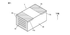
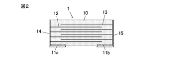
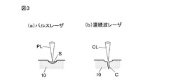
- FIG. 1 is a perspective view of a multilayer ceramic capacitor which is a first embodiment of a ceramic electronic component according to the present invention. It is sectional drawing of the multilayer ceramic capacitor shown in FIG. It is the schematic which shows the state at the time of irradiating a pulsed laser and a continuous wave laser to a titanium metal oxide. It is a figure which shows the power change of a pulse laser.
- FIG. 1 and 2 show a multilayer ceramic capacitor 1 which is a first embodiment of a ceramic electronic component according to the present invention.
- the bottom surface of the capacitor 1 is shown facing upward.
- Capacitor 1 is formed in a substantially rectangular parallelepiped ceramic body 10, a plurality of internal electrodes 12 and 13 that are formed inside ceramic body 10 and are alternately drawn on both end faces, and both end faces and bottom faces.
- the formed external electrodes 14 and 15 are provided.
- the drawings including FIG. 1 are all schematic, and the dimensions, aspect ratio scales, and the like may differ from actual products.
- the ceramic body 10 is made of a sintered ceramic material containing a titanium-based metal oxide such as BaTiO 3 .
- low resistance portions 11 a and 11 b are formed at both ends of the bottom surface of the ceramic body 10, that is, in the vicinity of both end surfaces on the bottom surface side.
- the low resistance parts 11a and 11b are made of titanium-based metal oxides that are modified by irradiation with a pulse laser, which will be described later, to make an n-type semiconductor.
- BaTiO 3 it is considered that the following reaction occurs by irradiation with a pulse laser.
- BaTiO X is a kind of semiconductor, and x is larger than 2 and smaller than 3.
- the plated metal can be deposited on the low resistance portions 11a and 11b by performing electrolytic plating.
- the external electrodes 14 and 15 made of plated metal are continuously formed on both end faces of the ceramic body 10 and the low resistance portions 11a and 11b. This is because the end portions of the plurality of internal electrodes 12 and 13 are exposed at both end faces of the ceramic body 10, so that the plated metal can be deposited without particularly reducing the resistance. It goes without saying that low resistance portions may be formed on both end faces as required.
- the external electrodes 14 and 15 are L-shaped when viewed from the front, but the U-shaped external electrodes are formed by forming the low resistance portions 11a and 11b also on the upper surface side. Is also possible. In addition, by selecting a pulse laser irradiation range, a low resistance portion can be formed at an arbitrary portion, and an external electrode can be formed at an arbitrary portion.
- the external electrodes 14 and 15 are formed by a single plating layer, but may be formed by a plurality of plating layers. For example, a plating layer serving as a base may be formed on the low resistance portions 11a and 11b, and a plating layer made of another metal may be formed thereon for the purpose of improving corrosion resistance and solder wettability.
- the material and the number of plating layers constituting the external electrodes 14 and 15 are arbitrary.
- FIG. 3 shows an example of laser irradiation for forming a low resistance portion in the surface layer portion of the ceramic body 10 made of a titanium-based metal oxide.
- FIG. 3A shows a cross section of the surface layer portion when irradiated with the pulse laser PL
- FIG. 3B shows a cross section of the surface layer portion when irradiated with the continuous wave laser CL.
- a continuous wave laser if the output is low, the resistance is not reduced. Conversely, if the output is increased, cracks C are likely to occur.
- FIG. 3B shows a state in which a crack C has occurred.
- the low resistance portion S can be formed without causing cracks by appropriately selecting the peak power density and frequency.
- the pulse laser can concentrate the energy within a short time width, so that a high peak output can be obtained.
- d is the pulse width
- the height h is the peak power
- the area (d ⁇ h) is the peak energy.
- the broken line is the average output. Dividing the peak energy by the laser spot diameter gives the pulse power density, that is, the peak energy density. The following relationship exists between the average power density and the peak power density of the pulse laser.
- Average power density (W / cm 2 ) peak power density (W / cm 2 ) x pulse width (s) x frequency (Hz)
- a pulse laser irradiation experiment was performed using a BaTiO 3 ceramic single plate as a base material and changing the peak power density and frequency.
- a YVO 4 fiber laser was used as the pulse laser, the laser scanning conditions were 100 mm / s, and the pitch interval was 30 ⁇ m.
- the laser irradiation range was a square area of 5 mm ⁇ 5 mm.
- the resistance of the portion irradiated with the laser was measured to check whether the resistance was reduced. The results are shown in Table 1. The ⁇ marks in the results indicate that the low resistance portion could be formed.
- the resistance of the surface layer portion of the BaTiO 3 ceramic single plate can be reduced by an appropriate combination of peak power density and frequency. That is, when the peak power density of the pulse laser is 1 ⁇ 10 6 W / cm 2 to 1 ⁇ 10 9 W / cm 2 and the frequency is 500 kHz or less, the low resistance portion can be formed. Even if the peak power density is appropriate, if the frequency is too high, the next pulsed light may be irradiated with insufficient cooling of the surface once heated, and cracks may occur due to heat accumulation. When irradiation was performed at a peak power density lower than the above range, a low resistance portion could not be formed or a crack occurred.
- the same BaTiO 3 ceramic single plate as described above was used, and an irradiation experiment of a continuous wave laser was performed by changing the average power density.
- a Yb fiber laser was used, the scanning speed was 100 mm / s, and the pitch interval was 30 ⁇ m.
- the laser irradiation range was a square area of 5 mm ⁇ 5 mm. The results are shown in Table 2.
- a pulsed laser was irradiated to the ceramic body 10 based on BaTiO 3 only on both ends of the bottom surface under the conditions described in Table 3.
- the ceramic body 10 irradiated with laser was subjected to electrolytic Ni plating under the conditions shown in Table 4, Ni was continuously deposited on the laser irradiated portion (low resistance portion) and both end faces where the internal electrodes were exposed. Ni plating does not precipitate unless the degree of resistance reduction is particularly large.
- a low resistance portion having a low resistance value was formed, so that a good plated electrode could be formed.
- a ceramic body 10 based on BaTiO 3 was irradiated with a YVO 4 solid SHG laser (wavelength: 532 nm) under the conditions shown in Table 5.
- An attenuator was used during irradiation.
- the peak power density is a value that takes into account the attenuation of light by the attenuator.
- the irradiation range is the same as in Example 2.
- Cu plating was deposited on the irradiated portion (low resistance portion) and both end faces.
- the irradiation pitch of the pulse laser may be smaller or larger than the spot diameter of the laser irradiation. That is, the low resistance part does not need to overlap with each other, and may be separated by a predetermined distance. Even if the low resistance portions are separated from each other, since the plating grows in a planar shape with the metal deposited on the low resistance portion by electrolytic plating as a nucleus, a continuous electrode can be formed.
- the present invention is applied to the formation of the external electrode of the multilayer ceramic capacitor.
- the electronic component targeted by the present invention is not limited to a multilayer ceramic capacitor, but can be applied to any ceramic electronic component made of a titanium-based metal oxide capable of forming a semiconductor portion (low resistance portion) by irradiation with a pulse laser. It is. That is, the material of the ceramic body is not limited to BaTiO 3 .
- a single pulse laser may be dispersed to irradiate a plurality of locations simultaneously with the laser. Furthermore, the laser irradiation range may be widened by shifting the focus of the laser as compared with the case where the laser is in focus.
- the present invention is not limited to the case where all the electrodes formed on the surface layer portion of the ceramic body are composed of only plated electrodes. That is, the present invention can also be applied when the electrode is formed of a plurality of materials.
- a base electrode is formed on a part of the ceramic surface using conductive paste, sputtering, vapor deposition, etc., and a low resistance portion is formed in a portion adjacent to the base electrode, and continuous on the low resistance portion and the base electrode.
- a plating electrode may be formed on the substrate.
- the application site of the low resistance portion can be arbitrarily selected.
Landscapes
- Engineering & Computer Science (AREA)
- Power Engineering (AREA)
- Chemical & Material Sciences (AREA)
- Microelectronics & Electronic Packaging (AREA)
- Manufacturing & Machinery (AREA)
- Electrochemistry (AREA)
- Chemical Kinetics & Catalysis (AREA)
- Materials Engineering (AREA)
- Metallurgy (AREA)
- Organic Chemistry (AREA)
- Ceramic Engineering (AREA)
- Inorganic Chemistry (AREA)
- Physics & Mathematics (AREA)
- Electromagnetism (AREA)
- Optics & Photonics (AREA)
- Ceramic Capacitors (AREA)
- Fixed Capacitors And Capacitor Manufacturing Machines (AREA)
Abstract
【課題】 チタンを含む金属酸化物からなるセラミック素体の表面の任意の部位にめっき電極を形成できるセラミック電子部品の製造方法、及びセラミック電子部品を提案する。 【解決手段】 チタンを含む金属酸化物を含有するセラミック素体10を準備する工程と、セラミック素体の表層部の一部にピークパワー密度1×10⁶W/cm2~1×109W/cm2、周波数500kHz以下のパルスレーザを照射し、金属酸化物を改質して低抵抗部を形成する工程と、低抵抗部上に電極を電解めっき処理により形成する工程と、を備えるセラミック電子部品の製造方法である。BaTiO3のようなチタンを含む金属酸化物は、レーザ照射による加熱でO欠陥が生成され、n型半導体が形成される。この半導体部分は金属酸化物より抵抗値が低いので、電解めっきによりめっき金属を選択的に析出させることができる。
Description
本発明はセラミック電子部品の製造方法、特にセラミック素体の表面にめっき電極を形成する方法及びセラミック電子部品に関する。
従来から、電子部品の外部電極の形成方法は、セラミック素体の両端面に電極ペーストを塗布し、次に電極ペーストを焼付け又は熱硬化することで下地電極を形成した後、その下地電極の上にめっき処理によってめっき電極を形成するのが一般的である。
電極ペーストの塗布は、所定の厚みで形成したペースト膜に電子部品の端部を浸漬する方法や、ローラ等による転写を利用した方法が用いられる。これらの技術では、電極ペーストを塗布する関係で、電極の厚みが大きくなり、その分だけ外形寸法が増大するという課題がある。
このような電極ペーストを用いた電極形成方法に代えて、内部電極の複数の端部をセラミック素体の端面に互いに近接して露出させると共に、アンカータブと呼ばれるダミー端子を内部電極の端部と同じ端面に近接して露出させ、セラミック素体に対して無電解めっきを行うことにより、これら内部電極の端部とアンカータブとを核としてめっき金属を成長させ、外部電極を形成する方法が提案されている(特許文献1)。この方法であれば、めっき処理だけで外部電極を形成可能となる。
しかし、この工法では、めっきを析出させるための核として、複数の内部電極の端部とアンカータブとをセラミック素体の端面に近接して露出させる必要があるため、製造工程が複雑になり、コスト上昇に至るという欠点を有する。しかも、内部電極の端部が露出する面にしか外部電極を形成できないため、外部電極の形成部位が制約されるという問題がある。
そこで、本出願人は、金属酸化物(特にフェライト)を含有した焼結済みセラミックの表面にレーザを照射することにより、金属酸化物の一部を還元して低抵抗部を形成し、その低抵抗部上にめっき電極を形成する電極形成方法を提案した(特許文献2)。この方法を用いることで、電子部品の表面の任意の部位にめっき電極を形成することができる。
特許文献2では、金属酸化物として主にフェライトを対象としており、フェライトに含まれるFe酸化物をレーザ照射により還元し、低抵抗部を形成することを主眼としている。一方、積層セラミックコンデンサ等に使用されるBaTiO3のようなチタンを含む金属酸化物においても、レーザ照射によってめっきを析出できる低抵抗部を形成する適切な方法が求められる。
本発明の目的は、チタンを含む金属酸化物からなるセラミック素体の表面の任意の部位にめっき電極を形成できるセラミック電子部品の製造方法、及びセラミック電子部品を提案するものである。
前記目的を達成するため、本発明の第1の態様は、チタンを含む金属酸化物を含有するセラミック素体を準備する工程と、前記セラミック素体の表層部の一部にパルスレーザを照射し、前記金属酸化物を改質して低抵抗部を形成する工程と、前記低抵抗部上に電極を電解めっき処理により形成する工程と、を備え、前記パルスレーザを、ピークパワー密度1×10⁶W/cm2~1×109W/cm2、周波数500kHz以下で照射することを特徴とする、セラミック電子部品の製造方法を提供する。
本発明の第2の態様は、チタンを含む金属酸化物を含有したセラミック素体と、前記セラミック素体の表層部の一部に形成され、前記金属酸化物が改質された低抵抗部と、前記低抵抗部上に形成されためっき金属からなる電極と、を備え、前記低抵抗部では金属酸化物がn型半導体化している、ことを特徴とするセラミック電子部品を提供する。
本発明は以下の知見に基づく。チタンを含む金属酸化物(以下ではチタン系金属酸化物と呼ぶ)を含有したセラミック素体の表層部にレーザを照射すると、めっき金属を形成するための低抵抗部を形成できないか、又はクラックが発生することがある。その理由は、BaTiO3のようなチタン系金属酸化物は、金属イオンと酸化物イオンとの結合力が強いため、低出力のレーザを照射しただけでは還元せず、低抵抗化が困難であるからと考えられる。一方、高出力のレーザを使用したとしても、金属酸化物がアブレーションしてしまったり、クラックが発生したりするため、製品としての特性悪化を招くという問題がある。そこで、レーザとしてパルスレーザを使用し、ピークパワー密度、周波数という2つのパラメータに注目することで、めっき電極を析出可能な低抵抗部を形成することができた。
低抵抗部の形成メカニズムは以下のように推測される。すなわち、BaTiO3のようなチタン系金属酸化物は、レーザ照射による加熱でO欠陥が生成され、余剰となった電子がチタン系金属酸化物の伝導体を流れる、いわゆるn型半導体になる。パルスレーザは、短い時間幅の中にエネルギーを集中させることができるため 高いピーク出力を得ることができる。パルスとパルスの時間間隔により、金属酸化物の表面近傍のみの過熱と冷却とが繰り返され、過剰に熱が行き渡らないため、クラックやアブレーションを生じることなく低抵抗化(半導体化)が可能になる。
パルスレーザの照射には適切な条件(ピークパワー密度、周波数などのパラメータ)が存在する。具体的には、パルスレーザを、ピークパワー密度1×10⁶W/cm2~1×109W/cm2、周波数500kHz以下の条件で照射した場合に良好な結果が得られる。上記のピークパワー密度より低いピークパワー密度で照射すると、チタン系金属酸化物が全く半導体化しなかったり、又はO欠陥が生じる温度に達するまでに時間を要するので、熱拡散により表面から比較的深くまで加熱されてしまったりする。その場合、熱影響を受ける範囲が広くなるため、体積膨張によりクラックが生じることがある。クラックが発生すると、たとえ低抵抗部が形成されても、抵抗値が高くなるためめっきできなくなる。一方、上記より高いピークパワー密度で照射すると、短時間で表面近傍の温度が上昇するため、O欠陥が生じる温度領域を超え、クラックが発生したり、金属酸化物が気化し飛散する、いわゆるアブレーションが発生したりすることがある。よって、パルスレーザのピークパワー密度を適切に調節することで、クラックやアブレーションの発生を抑制しながら、チタン系金属酸化物の半導体化が可能になる。
パルスレーザの周波数を変更すると、パルスとパルスの時間間隔が変化する。ピークパワー密度が適切であったとしても、周波数が高すぎる(パルスとパルスの時間間隔が短過ぎる)と、一度加熱された表面の冷却が不十分なまま次のパルスが照射され、熱蓄積によりクラックが生じてしまう可能性がある。なお、周波数を極端に低くしたとしても、低抵抗化において特に問題はないと考えられるが、レーザ照射の処理時間の増加を招き、実質的に工業的に用いることが困難になる。
パルスレーザの照射条件を、ピークパワー密度1×10⁶W/cm2~1×108W/cm2、周波数10kHz~100kHzとした場合には、微細なクラックの発生を抑制でき、めっき析出性の良好な低抵抗部を形成できる。パルスレーザとしては、YVO4レーザ、YAGレーザなど公知のレーザを使用できる。
パルスレーザの照射により低抵抗部を形成可能なチタン系金属酸化物としては、例えば積層セラミックコンデンサに使用されるBaTiO3がある。なお、BaTiO3以外にも、SrTiO3、TiO2、PbTiO3、PZT、PLZT、K2Ti6O13、Ba2Ti9O20のような他のチタン系金属酸化物でも、パルスレーザを照射することにより低抵抗部を形成可能である。
本発明を積層セラミックコンデンサの外部電極形成に適用することができる。積層セラミックコンデンサの場合、セラミック電子部品の両端面には複数の内部電極の端部が露出しており、セラミック電子部品の両端面に隣接する少なくとも1つの側面であって、両端面との近傍部分に低抵抗部を形成し、めっき金属からなる電極を、セラミック電子部品の両端面と低抵抗部上とに連続的に形成した構造としてもよい。すなわち、低抵抗部を、内部電極の端部が露出した両端面に隣接する側面であって、両端面との近傍部分に形成した場合、このセラミックコンデンサをめっき浴の中に入れて電解めっきを行うことにより、セラミック電子部品の両端面と低抵抗部上とに連続的にめっき電極を形成することができる。両端面には複数の内部電極の端部が露出しているので、格別な低抵抗化を行わなくても、めっき電極を形成可能である。つまり、両端面と低抵抗部とに個別の電極を形成する必要がなく、1回のめっき処理で外部電極を形成可能になる。なお、必要に応じて、内部電極の端部が露出した両端面の一部又は全部にも低抵抗部を形成してもよい。
本発明の「低抵抗部」とは、パルスレーザを照射していない部分(酸化物)に比べて抵抗値の低い部分(一種の半導体)を指す。低抵抗部は面状に連続している必要はなく、複数の部分が独立していてもよい。上述のように低抵抗部は他の表面部分に比べて抵抗値が低いので、めっき金属が析出しやすく、析出した金属が核となって成長するので、連続した電極を容易に形成できる。低抵抗部はパルスレーザを照射できる領域であれば任意の部位に形成できるので、めっき電極も電子部品の任意の部位に形成できる。しかも、めっき処理は1回で多数個の部品を同時に処理できるので、非常に効率的かつ工業的に安価である。
本発明において「めっき金属からなる電極」とは、外部電極に限らず、任意の電極であってもよい。例えば、パッド電極、ランド電極、コイル状電極、回路パターン電極であってもよい。さらに、セラミック電子部品とは、チップ部品に限らず、回路モジュールのような複合部品であってもよいし、回路基板や多層基板であってもよい。
以上のように、本発明によれば、チタン系金属酸化物からなるセラミック素体の表層部に、ピークパワー密度、周波数という2つの適切なパラメータを満足するパルスレーザを照射することで、チタン系金属酸化物を半導体化して低抵抗部を形成できる。この低抵抗部上に電極を電解めっき処理により形成することで、電子部品の表面の任意の部分に電極を形成できる。特に、チタン系金属酸化物は、還元しにくく、クラック又はアブレーションが発生しやすいという性質があるが、所定条件のパルスレーザを使用することにより、めっき電極が析出する低抵抗部を形成することが可能になる。
図1、図2は本発明に係るセラミック電子部品の第1実施例である積層セラミックコンデンサ1を示す。なお、図1ではコンデンサ1の底面が上向きとなるように表されている。コンデンサ1は、略直方体形状のセラミック素体10と、セラミック素体10の内部に形成され、両端面に交互に引き出された複数の内部電極12、13と、両端面と底面とに連続的に形成された外部電極14、15とを備えている。なお、図1を含め図面はすべて模式的なものであり、その寸法や縦横比の縮尺などは実際の製品とは異なる場合がある。
セラミック素体10は、例えばBaTiO3などのチタン系金属酸化物を含有する焼結済みセラミック材料からなる。図2に示すように、セラミック素体10の底面の両端部、つまり底面側の両端面との近傍部分に低抵抗部11a、11bが形成されている。低抵抗部11a、11bは、チタン系金属酸化物が後述するパルスレーザの照射によって改質されてn型半導体化したものである。
例えばBaTiO3の場合、パルスレーザの照射により次のような反応が生じると考えられる。
BaTiO3+パルスレーザ→BaTiOX+O2↑
ここで、BaTiOXは一種の半導体であり、xは2より大きく、3より小さい。
BaTiO3+パルスレーザ→BaTiOX+O2↑
ここで、BaTiOXは一種の半導体であり、xは2より大きく、3より小さい。
低抵抗部11a、11bはその他の部分(金属酸化物)に比べて抵抗値が低いので、電解めっきを行うことで、めっき金属を低抵抗部11a,11b上に析出させることができる。めっき金属からなる外部電極14、15は、セラミック素体10の両端面と低抵抗部11a,11b上とに連続的に形成されている。セラミック素体10の両端面には複数の内部電極12、13の端部が露出しているので、格別な低抵抗化を行わなくても、めっき金属を析出可能だからである。なお、必要に応じて、両端面に低抵抗部を形成してもよいことは勿論である。
この実施形態では、外部電極14、15が正面視においてL字形状のものを示したが、低抵抗部11a,11bを上面側にも形成することで、コ字形状の外部電極を形成することも可能である。その他、パルスレーザの照射範囲を選定することにより、任意の部位に低抵抗部を形成でき、ひいては任意の部位に外部電極を形成できる。図2では、外部電極14、15が一層のめっき層で形成されているが、複数層のめっき層で形成されてもよい。例えば、低抵抗部11a,11b上に下地となるめっき層を形成し、その上に耐食性やはんだ濡れ性を向上させる目的で別の金属からなるめっき層を形成してもよい。外部電極14,15を構成するめっき層の材料及び層数は任意である。
図3は、チタン系金属酸化物からなるセラミック素体10の表層部に低抵抗部を形成するためのレーザ照射の例を示す。図3の(a)はパルスレーザPLを照射した場合の表層部の断面を示し、図3の(b)は連続波レーザCLを照射した場合の表層部の断面を示す。連続波レーザの場合、出力が低いと低抵抗化せず、逆に出力を高くすると、クラックCが発生しやすい。図3の(b)はクラックCが発生した状態を示す。一方、パルスレーザの場合には、ピークパワー密度及び周波数を適切に選択することにより、クラックを発生させずに低抵抗部Sを形成することが可能になる。
パルスレーザは、図4のように、短い時間幅の中にエネルギーを集中させることができるため 高いピーク出力を得ることができる。dはパルス幅、高さhがピークパワーであり、面積(d×h)がピークエネルギーとなる。破線は平均出力である。ピークエネルギーをレーザスポット径で割ると、パルスパワー密度、つまりピークエネルギー密度となる。パルスレーザの平均パワー密度とピークパワー密度との間には以下の関係が存在する。
平均パワー密度(W/cm2)=ピークパワー密度(W/cm2)×パルス幅(s)×周波数(Hz)
平均パワー密度(W/cm2)=ピークパワー密度(W/cm2)×パルス幅(s)×周波数(Hz)
-実施例1-
次に、BaTiO3系セラミック単板を基材とし、ピークパワー密度と周波数とを変化させてパルスレーザの照射実験を行った。パルスレーザとしてYVO4ファイバーレーザを使用し、レーザの走査条件は100mm/s、ピッチ間隔は30μmとした。レーザ照射範囲は5mm×5mmの四角形領域とした。レーザ照射した箇所の抵抗を測定し、低抵抗化しているか調べた。その結果を、表1に示す。結果の○印は、低抵抗部を形成できたことを示す。
次に、BaTiO3系セラミック単板を基材とし、ピークパワー密度と周波数とを変化させてパルスレーザの照射実験を行った。パルスレーザとしてYVO4ファイバーレーザを使用し、レーザの走査条件は100mm/s、ピッチ間隔は30μmとした。レーザ照射範囲は5mm×5mmの四角形領域とした。レーザ照射した箇所の抵抗を測定し、低抵抗化しているか調べた。その結果を、表1に示す。結果の○印は、低抵抗部を形成できたことを示す。

以上の実験結果から、ピークパワー密度と周波数の適切な組み合わせで、BaTiO3系セラミック単板の表層部を低抵抗化できることがわかる。すなわち、パルスレーザのピークパワー密度を1×10⁶W/cm2~1×109W/cm2、周波数を500kHz以下とした場合に、低抵抗部を形成可能である。ピークパワー密度が適切であっても、周波数が大きすぎると、一度加熱された表面の冷却が不十分なまま次のパルス光が照射され、熱蓄積によりクラックが生じることがある。上記の範囲より低いピークパワー密度で照射すると、低抵抗部が形成できないか、又はクラックが発生した。一方、高いピークパワー密度で照射すると、クラック又はアブレーションが発生した。なお、波長による影響は大きくないと言える。上記範囲のうち、特にパルスレーザのピークパワー密度を1×106W/cm2~1×108W/cm2、周波数を10kHz~100kHzとした場合に、微細なクラックの発生を抑制しながらめっき析出性のよい低抵抗部を形成できる。
比較のために、上記と同じBaTiO3系セラミック単板を使用し、平均パワー密度を変化させて連続波レーザの照射実験を行った。具体的にはYbファイバーレーザを使用し、走査速度は100mm/s、ピッチ間隔は30μmとした。レーザ照射範囲は5mm×5mmの四角形領域とした。その結果を、表2に示す。
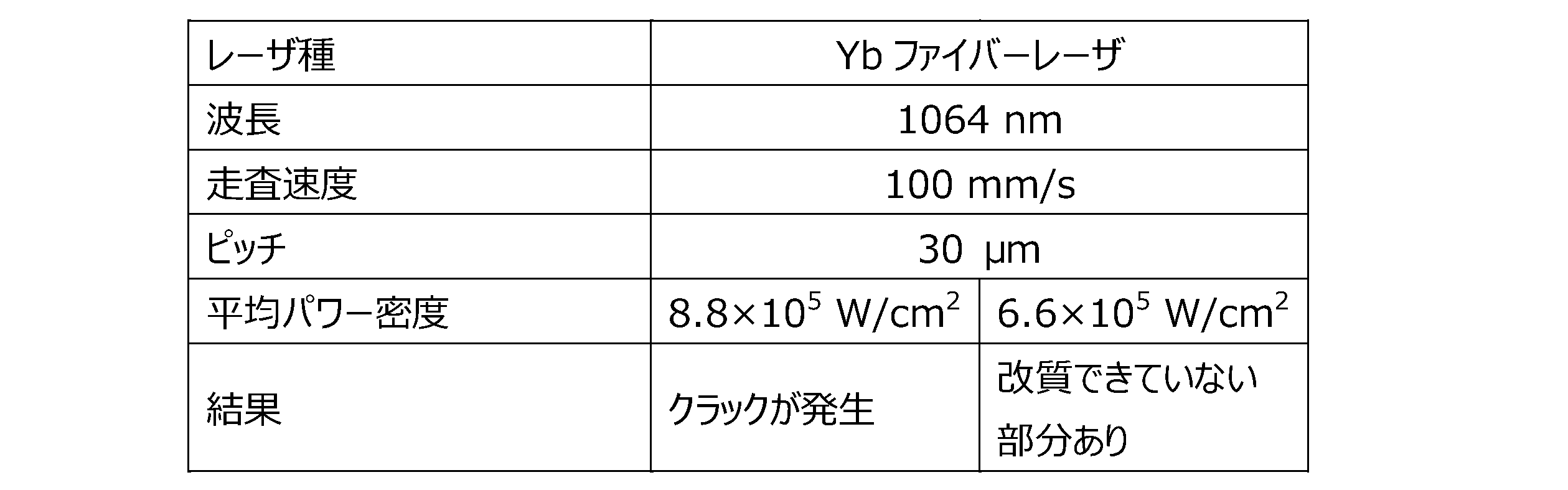
表2の結果から明らかなように、8.8×10⁵W/cm2の連続波レーザを照射した場合には、クラックが発生し、6.6×105W/cm2の連続波レーザを照射した場合には低抵抗部を形成できなかった。
-実施例2-
図1、図2に示したように、BaTiO3を基材とするセラミック素体10に対し、その底面の両端部のみにパルスレーザを表3に記載した条件で照射した。レーザ照射したセラミック素体10を表4の条件で電解Niめっきしたところ、レーザ照射箇所(低抵抗部)と内部電極が露出した両端面とにNiが連続的に析出した。Niめっきは特に低抵抗化度が大きくなければ析出しない。表3の条件の場合、抵抗値の低い低抵抗部が形成されたため、良好なめっき電極を形成できた。
図1、図2に示したように、BaTiO3を基材とするセラミック素体10に対し、その底面の両端部のみにパルスレーザを表3に記載した条件で照射した。レーザ照射したセラミック素体10を表4の条件で電解Niめっきしたところ、レーザ照射箇所(低抵抗部)と内部電極が露出した両端面とにNiが連続的に析出した。Niめっきは特に低抵抗化度が大きくなければ析出しない。表3の条件の場合、抵抗値の低い低抵抗部が形成されたため、良好なめっき電極を形成できた。


-実施例3-
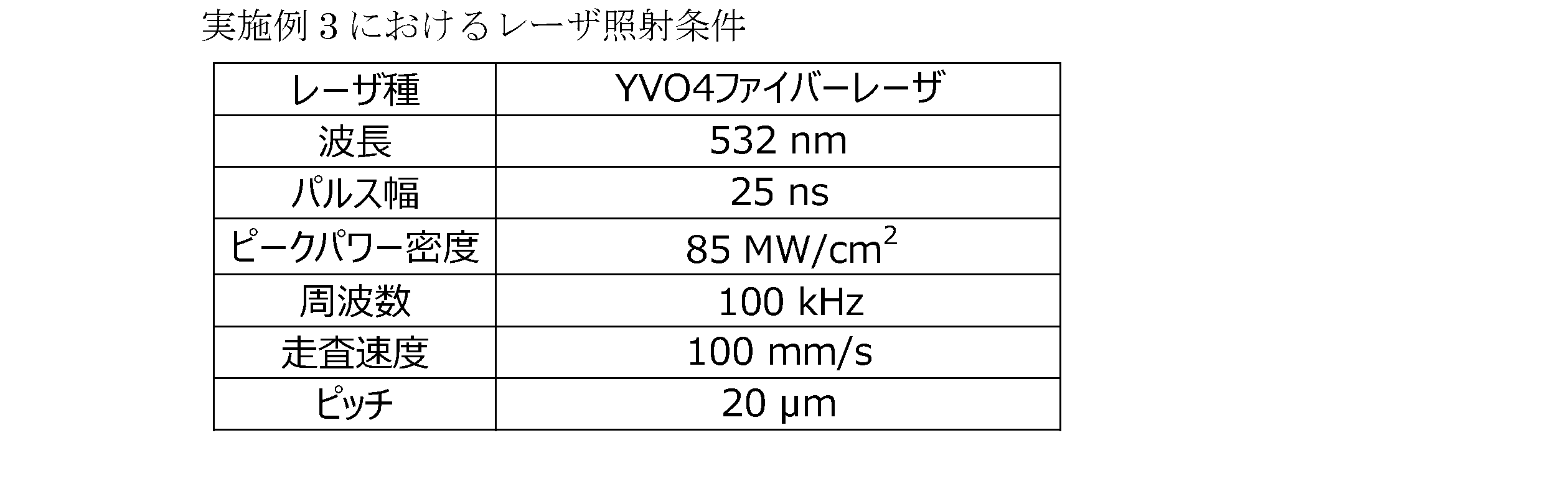
図1、図2に示したように、BaTiO3を基材とするセラミック素体10にYVO4固体SHGレーザ(波長:532nm)を表5の条件で照射した。照射の際アッテネータを使用した。なお、ピークパワー密度はアッテネータによる光の減衰を考慮した値である。照射範囲は実施例2と同様である。レーザ照射したセラミック素体10を表6の条件で電解Cuめっきしたところ、照射部(低抵抗部)及び両端面にCuめっきが析出した。
図1、図2に示したように、BaTiO3を基材とするセラミック素体10にYVO4固体SHGレーザ(波長:532nm)を表5の条件で照射した。照射の際アッテネータを使用した。なお、ピークパワー密度はアッテネータによる光の減衰を考慮した値である。照射範囲は実施例2と同様である。レーザ照射したセラミック素体10を表6の条件で電解Cuめっきしたところ、照射部(低抵抗部)及び両端面にCuめっきが析出した。

パルスレーザの照射ピッチは、レーザ照射のスポット径より小さくても、大きくてもよい。つまり、低抵抗部は、隣り合う低抵抗部同士が重なる必要はなく、所定距離だけ離れていてもよい。低抵抗部同士が離間していても、電解めっきにより低抵抗部上に析出した金属を核としてめっきが平面状に成長するので、連続した電極を形成できる。
上記実施例では、本発明を積層セラミックコンデンサの外部電極の形成に適用した例を示したが、これに限るものではない。本発明が対象とする電子部品としては、積層セラミックコンデンサに限らず、パルスレーザの照射によって半導体部(低抵抗部)が形成され得るチタン系金属酸化物からなるセラミック電子部品であれば、適用可能である。すなわち、セラミック素体の材質はBaTiO3に限定されない。
低抵抗部を形成するために、1本のパルスレーザを分光して、複数箇所に同時にレーザを照射してもよい。さらに、レーザの焦点をずらして、レーザの焦点が合っている場合に比べて、レーザの照射範囲を広げてもよい。
本発明は、セラミック素体の表層部に形成されるすべての電極がめっき電極だけで構成される場合に限らない。つまり、電極が複数の材料で形成された場合にも適用できる。例えば、セラミックの表面の一部に導電ペースト、スパッタ、蒸着などを用いて下地電極を形成し、それと隣接する部位に低抵抗部を形成し、その低抵抗部と下地電極との上に連続的にめっき電極を形成してもよい。その他、低抵抗部の適用部位は任意に選択できる。
1 電子部品(積層セラミックコンデンサ)
10 セラミック素体
11a,11b 低抵抗部
12、13 内部電極
14、15 外部電極(めっき電極)
PL パルスレーザ
10 セラミック素体
11a,11b 低抵抗部
12、13 内部電極
14、15 外部電極(めっき電極)
PL パルスレーザ
Claims (8)
- チタンを含む金属酸化物を含有するセラミック素体を準備する工程と、
前記セラミック素体の表層部の一部にパルスレーザを照射し、前記金属酸化物を改質して低抵抗部を形成する工程と、
前記低抵抗部上に電極を電解めっき処理により形成する工程と、
を備え、
前記パルスレーザを、ピークパワー密度1×10⁶W/cm2~1×109W/cm2、周波数500kHz以下で照射することを特徴とする、セラミック電子部品の製造方法。 - 前記低抵抗部では、前記金属酸化物がn型半導体化している、請求項1に記載のセラミック電子部品の製造方法。
- 前記パルスレーザを、ピークパワー密度1×10⁶W/cm2~1×108W/cm2、周波数10kHz~100kHzで照射することを特徴とする、請求項1又は2に記載のセラミック電子部品の製造方法。
- 前記セラミック素体はBaTiO3を含有している、請求項1乃至3のいずれか1項に記載のセラミック電子部品の製造方法。
- 前記セラミック電子部品は積層セラミックコンデンサであり、
前記セラミック電子部品の両端面には複数の内部電極の端部が露出しており、
前記セラミック電子部品の両端面に隣接する少なくとも1つの側面であって、前記両端面との近傍部分に前記低抵抗部が形成され、
前記電極は、前記セラミック電子部品の両端面と前記低抵抗部上とに連続的に形成されている、
請求項1乃至4のいずれか1項に記載のセラミック電子部品の製造方法。 - チタンを含む金属酸化物を含有したセラミック素体と、
前記セラミック素体の表層部の一部に形成され、前記金属酸化物が改質された低抵抗部と、
前記低抵抗部上に形成されためっき金属からなる電極と、を備え、
前記低抵抗部では金属酸化物がn型半導体化している、ことを特徴とするセラミック電子部品。 - 前記セラミック素体はBaTiO3を含有している、請求項6に記載のセラミック電子部品。
- 前記セラミック電子部品は積層セラミックコンデンサであり、
前記セラミック電子部品の両端面には複数の内部電極の端部が露出しており、
前記セラミック電子部品の両端面に隣接する少なくとも1つの側面であって、前記両端面との近傍部分に前記低抵抗部が形成され、
前記めっき金属からなる電極は、前記セラミック電子部品の両端面と前記低抵抗部上とに連続的に形成されている、
請求項6又は7に記載のセラミック電子部品。
Priority Applications (3)
| Application Number | Priority Date | Filing Date | Title |
|---|---|---|---|
| CN201880010637.5A CN110268489B (zh) | 2017-05-31 | 2018-02-05 | 陶瓷电子部件的制造方法以及陶瓷电子部件 |
| JP2019521953A JP6791378B2 (ja) | 2017-05-31 | 2018-02-05 | セラミック電子部品の製造方法 |
| US16/666,177 US10971305B2 (en) | 2017-05-31 | 2019-10-28 | Method for manufacturing ceramic electronic component and ceramic electronic component |
Applications Claiming Priority (2)
| Application Number | Priority Date | Filing Date | Title |
|---|---|---|---|
| JP2017107346 | 2017-05-31 | ||
| JP2017-107346 | 2017-05-31 |
Related Child Applications (1)
| Application Number | Title | Priority Date | Filing Date |
|---|---|---|---|
| US16/666,177 Continuation US10971305B2 (en) | 2017-05-31 | 2019-10-28 | Method for manufacturing ceramic electronic component and ceramic electronic component |
Publications (1)
| Publication Number | Publication Date |
|---|---|
| WO2018220901A1 true WO2018220901A1 (ja) | 2018-12-06 |
Family
ID=64455792
Family Applications (1)
| Application Number | Title | Priority Date | Filing Date |
|---|---|---|---|
| PCT/JP2018/003751 Ceased WO2018220901A1 (ja) | 2017-05-31 | 2018-02-05 | セラミック電子部品の製造方法及びセラミック電子部品 |
Country Status (4)
| Country | Link |
|---|---|
| US (1) | US10971305B2 (ja) |
| JP (1) | JP6791378B2 (ja) |
| CN (1) | CN110268489B (ja) |
| WO (1) | WO2018220901A1 (ja) |
Cited By (4)
| Publication number | Priority date | Publication date | Assignee | Title |
|---|---|---|---|---|
| WO2022163193A1 (ja) * | 2021-01-29 | 2022-08-04 | 株式会社村田製作所 | セラミック電子部品 |
| US12340947B2 (en) | 2022-03-26 | 2025-06-24 | Murata Manufacturing Co., Ltd. | Multilayer ceramic capacitor |
| US12374489B2 (en) | 2022-11-30 | 2025-07-29 | Samsung Electro-Mechanics Co., Ltd. | Multilayer electronic component |
| US12505954B2 (en) | 2023-11-16 | 2025-12-23 | Samsung Electro-Mechanics Co., Ltd. | Multilayer ceramic capacitor |
Families Citing this family (4)
| Publication number | Priority date | Publication date | Assignee | Title |
|---|---|---|---|---|
| US11993840B2 (en) | 2021-06-17 | 2024-05-28 | Intalus, Inc. | Asynchronous conversion of metals to metal ceramics |
| KR102933569B1 (ko) | 2021-11-19 | 2026-03-04 | 삼성전기주식회사 | 적층 세라믹 전자부품 |
| KR102812715B1 (ko) * | 2021-12-30 | 2025-05-27 | 주식회사 아모텍 | 적층 세라믹 커패시터 및 그 제조방법 |
| KR20240147249A (ko) * | 2023-03-31 | 2024-10-08 | 삼성전기주식회사 | 적층형 전자 부품 |
Citations (4)
| Publication number | Priority date | Publication date | Assignee | Title |
|---|---|---|---|---|
| JPS6433084A (en) * | 1987-07-29 | 1989-02-02 | Tdk Corp | Partial modification method for oxide ceramic surface |
| JP2014065649A (ja) * | 2012-09-27 | 2014-04-17 | Seiren Co Ltd | セラミックスの表面改質方法 |
| JP2016004885A (ja) * | 2014-06-17 | 2016-01-12 | 株式会社村田製作所 | セラミック電子部品の製造方法 |
| JP2017011256A (ja) * | 2015-06-16 | 2017-01-12 | 株式会社村田製作所 | セラミック電子部品の製造方法及びセラミック電子部品 |
Family Cites Families (7)
| Publication number | Priority date | Publication date | Assignee | Title |
|---|---|---|---|---|
| US7152291B2 (en) | 2002-04-15 | 2006-12-26 | Avx Corporation | Method for forming plated terminations |
| US7897877B2 (en) * | 2006-05-23 | 2011-03-01 | Endicott Interconnect Technologies, Inc. | Capacitive substrate |
| CN101812684B (zh) * | 2010-04-19 | 2012-07-04 | 姚建华 | 一种金属表面激光强化涂层的制备方法 |
| WO2012023445A1 (ja) * | 2010-08-20 | 2012-02-23 | 株式会社 村田製作所 | 紫外線センサ、及び紫外線センサの製造方法 |
| WO2012056385A1 (en) * | 2010-10-25 | 2012-05-03 | Sabic Innovative Plastics Ip B.V. | Improved electroless plating performance of laser direct structuring materials |
| US10242789B2 (en) * | 2015-06-16 | 2019-03-26 | Murata Manufacturing Co., Ltd. | Method for manufacturing ceramic electronic component, and ceramic electronic component |
| CN106467965B (zh) * | 2016-09-27 | 2018-07-27 | 北京科技大学 | 一种陶瓷电路基板表面精细化金属图案的制备方法 |
-
2018
- 2018-02-05 JP JP2019521953A patent/JP6791378B2/ja active Active
- 2018-02-05 WO PCT/JP2018/003751 patent/WO2018220901A1/ja not_active Ceased
- 2018-02-05 CN CN201880010637.5A patent/CN110268489B/zh active Active
-
2019
- 2019-10-28 US US16/666,177 patent/US10971305B2/en active Active
Patent Citations (4)
| Publication number | Priority date | Publication date | Assignee | Title |
|---|---|---|---|---|
| JPS6433084A (en) * | 1987-07-29 | 1989-02-02 | Tdk Corp | Partial modification method for oxide ceramic surface |
| JP2014065649A (ja) * | 2012-09-27 | 2014-04-17 | Seiren Co Ltd | セラミックスの表面改質方法 |
| JP2016004885A (ja) * | 2014-06-17 | 2016-01-12 | 株式会社村田製作所 | セラミック電子部品の製造方法 |
| JP2017011256A (ja) * | 2015-06-16 | 2017-01-12 | 株式会社村田製作所 | セラミック電子部品の製造方法及びセラミック電子部品 |
Cited By (5)
| Publication number | Priority date | Publication date | Assignee | Title |
|---|---|---|---|---|
| WO2022163193A1 (ja) * | 2021-01-29 | 2022-08-04 | 株式会社村田製作所 | セラミック電子部品 |
| US12293875B2 (en) | 2021-01-29 | 2025-05-06 | Murata Manufacturing Co., Ltd. | Ceramic electronic component |
| US12340947B2 (en) | 2022-03-26 | 2025-06-24 | Murata Manufacturing Co., Ltd. | Multilayer ceramic capacitor |
| US12374489B2 (en) | 2022-11-30 | 2025-07-29 | Samsung Electro-Mechanics Co., Ltd. | Multilayer electronic component |
| US12505954B2 (en) | 2023-11-16 | 2025-12-23 | Samsung Electro-Mechanics Co., Ltd. | Multilayer ceramic capacitor |
Also Published As
| Publication number | Publication date |
|---|---|
| CN110268489A (zh) | 2019-09-20 |
| US20200066449A1 (en) | 2020-02-27 |
| US10971305B2 (en) | 2021-04-06 |
| JPWO2018220901A1 (ja) | 2019-11-07 |
| CN110268489B (zh) | 2021-07-20 |
| JP6791378B2 (ja) | 2020-11-25 |
Similar Documents
| Publication | Publication Date | Title |
|---|---|---|
| JP6791378B2 (ja) | セラミック電子部品の製造方法 | |
| US12014861B2 (en) | Method of manufacturing electronic component and electronic component | |
| US11322293B2 (en) | Method for manufacturing ceramic electronic component, and ceramic electronic component | |
| CN111261390B (zh) | 绕线型线圈部件以及绕线型线圈部件的制造方法 | |
| US8456796B2 (en) | Monolithic electronic component and method for manufacturing monolithic electronic component | |
| JP5471686B2 (ja) | 積層型セラミック電子部品の製造方法 | |
| TWI656547B (zh) | 陶瓷電子零件及其製造方法 | |
| JP2012099786A (ja) | 積層型セラミックキャパシタ及びその製造方法 | |
| JPWO2016133090A1 (ja) | チップ型電子部品およびモジュール | |
| JP2023158299A (ja) | 積層セラミック電子部品、回路基板及び積層セラミック電子部品の製造方法 | |
| JP2012142478A (ja) | 積層型電子部品およびその製造方法 | |
| JP6609137B2 (ja) | セラミック電子部品、及びその製造方法 | |
| US11821090B2 (en) | Method of manufacturing ceramic electronic component | |
| JP7280697B2 (ja) | 積層セラミックコンデンサの製造方法 | |
| JP2007110127A (ja) | 薄膜キャパシタの製造方法、それにより製造される薄膜キャパシタおよびこれを有する薄膜キャパシタ内蔵型印刷回路基板 | |
| JP5796643B2 (ja) | 積層型セラミック電子部品 | |
| JP5915798B2 (ja) | 積層型セラミック電子部品 | |
| JP2006173348A (ja) | 積層型圧電素子の製造方法 | |
| JP2018085437A (ja) | 電子部品の製造方法及び電子部品 | |
| JP2018060846A (ja) | 電子部品の製造方法 |
Legal Events
| Date | Code | Title | Description |
|---|---|---|---|
| 121 | Ep: the epo has been informed by wipo that ep was designated in this application |
Ref document number: 18810734 Country of ref document: EP Kind code of ref document: A1 |
|
| ENP | Entry into the national phase |
Ref document number: 2019521953 Country of ref document: JP Kind code of ref document: A |
|
| NENP | Non-entry into the national phase |
Ref country code: DE |
|
| 122 | Ep: pct application non-entry in european phase |
Ref document number: 18810734 Country of ref document: EP Kind code of ref document: A1 |