WO2018220717A1 - 電子装置およびその製造方法 - Google Patents
電子装置およびその製造方法 Download PDFInfo
- Publication number
- WO2018220717A1 WO2018220717A1 PCT/JP2017/020117 JP2017020117W WO2018220717A1 WO 2018220717 A1 WO2018220717 A1 WO 2018220717A1 JP 2017020117 W JP2017020117 W JP 2017020117W WO 2018220717 A1 WO2018220717 A1 WO 2018220717A1
- Authority
- WO
- WIPO (PCT)
- Prior art keywords
- main surface
- printed circuit
- connection land
- circuit board
- bonding material
- Prior art date
- Legal status (The legal status is an assumption and is not a legal conclusion. Google has not performed a legal analysis and makes no representation as to the accuracy of the status listed.)
- Ceased
Links
Images





Classifications
-
- H—ELECTRICITY
- H05—ELECTRIC TECHNIQUES NOT OTHERWISE PROVIDED FOR
- H05K—PRINTED CIRCUITS; CASINGS OR CONSTRUCTIONAL DETAILS OF ELECTRIC APPARATUS; MANUFACTURE OF ASSEMBLAGES OF ELECTRICAL COMPONENTS
- H05K1/00—Printed circuits
- H05K1/02—Details
- H05K1/14—Structural association of two or more printed circuits
-
- H—ELECTRICITY
- H05—ELECTRIC TECHNIQUES NOT OTHERWISE PROVIDED FOR
- H05K—PRINTED CIRCUITS; CASINGS OR CONSTRUCTIONAL DETAILS OF ELECTRIC APPARATUS; MANUFACTURE OF ASSEMBLAGES OF ELECTRICAL COMPONENTS
- H05K1/00—Printed circuits
- H05K1/02—Details
-
- H—ELECTRICITY
- H05—ELECTRIC TECHNIQUES NOT OTHERWISE PROVIDED FOR
- H05K—PRINTED CIRCUITS; CASINGS OR CONSTRUCTIONAL DETAILS OF ELECTRIC APPARATUS; MANUFACTURE OF ASSEMBLAGES OF ELECTRICAL COMPONENTS
- H05K3/00—Apparatus or processes for manufacturing printed circuits
- H05K3/22—Secondary treatment of printed circuits
- H05K3/28—Applying non-metallic protective coatings
-
- H—ELECTRICITY
- H05—ELECTRIC TECHNIQUES NOT OTHERWISE PROVIDED FOR
- H05K—PRINTED CIRCUITS; CASINGS OR CONSTRUCTIONAL DETAILS OF ELECTRIC APPARATUS; MANUFACTURE OF ASSEMBLAGES OF ELECTRICAL COMPONENTS
- H05K3/00—Apparatus or processes for manufacturing printed circuits
- H05K3/36—Assembling printed circuits with other printed circuits
-
- H—ELECTRICITY
- H05—ELECTRIC TECHNIQUES NOT OTHERWISE PROVIDED FOR
- H05K—PRINTED CIRCUITS; CASINGS OR CONSTRUCTIONAL DETAILS OF ELECTRIC APPARATUS; MANUFACTURE OF ASSEMBLAGES OF ELECTRICAL COMPONENTS
- H05K3/00—Apparatus or processes for manufacturing printed circuits
- H05K3/36—Assembling printed circuits with other printed circuits
- H05K3/368—Assembling printed circuits with other printed circuits parallel to each other
-
- H—ELECTRICITY
- H05—ELECTRIC TECHNIQUES NOT OTHERWISE PROVIDED FOR
- H05K—PRINTED CIRCUITS; CASINGS OR CONSTRUCTIONAL DETAILS OF ELECTRIC APPARATUS; MANUFACTURE OF ASSEMBLAGES OF ELECTRICAL COMPONENTS
- H05K1/00—Printed circuits
- H05K1/02—Details
- H05K1/0271—Arrangements for reducing stress or warp in rigid printed circuit boards, e.g. caused by loads, vibrations or differences in thermal expansion
-
- H—ELECTRICITY
- H05—ELECTRIC TECHNIQUES NOT OTHERWISE PROVIDED FOR
- H05K—PRINTED CIRCUITS; CASINGS OR CONSTRUCTIONAL DETAILS OF ELECTRIC APPARATUS; MANUFACTURE OF ASSEMBLAGES OF ELECTRICAL COMPONENTS
- H05K2201/00—Indexing scheme relating to printed circuits covered by H05K1/00
- H05K2201/09—Shape and layout
- H05K2201/09145—Edge details
- H05K2201/09172—Notches between edge pads
Definitions
- the present invention relates to an electronic device manufacturing method.
- a control IC for controlling a semiconductor switch element is mounted on a printed circuit board different from a printed circuit board on which a heat generating component such as a semiconductor switch element or a diode is mounted.
- Japanese Patent Application Laid-Open No. 11-103145 describes a circuit board in which two printed boards are directly joined with solder.
- the present invention provides a printed circuit board joining method, an electronic device, and an electronic device manufacturing method capable of easily confirming that two printed circuit boards are normally joined by soldering. With the goal.
- An electronic device is A first main land and a second main surface opposite to the first main surface, wherein a first connection land portion is provided at a side end of the first main surface; A first printed circuit board provided with a reference member on the connecting land portion of A third main surface and a fourth main surface opposite to the third main surface; the third main surface and the fourth main surface at a side edge of the fourth main surface; A second printed circuit board in which a second connection land portion is provided in the vicinity of the opening of the substrate through hole on the fourth main surface; A conductive bonding material that electrically connects between the first connection land portion and the second connection land portion; The reference member is configured to repel the conductive bonding material melted when the first printed circuit board and the second printed circuit board are bonded to each other.
- the first printed circuit board and the second printed circuit board are configured such that the side end of the first main surface and the side end of the fourth main surface face each other. Perpendicular to the first main surface that is joined by the conductive bonding material so as to be electrically connected to the second connecting land portion and passes through a reference interface between the reference member and the conductive bonding material. A normal line passes through the inside of the substrate through hole.
- the reference interface between the reference member and the conductive bonding material is visible from the third main surface side of the substrate through hole.
- At least a part of the conductive bonding material is located between an end of the first connection land portion and the second connection land portion.
- the reference member is a resist containing a resin.
- the conductive bonding material is a solder material.
- the thickness of the reference member is smaller than the distance between the surface of the first connection land portion and the surface of the second connection land portion.
- a plurality of the first connection land portions and reference members are provided along the side edges of the first main surface, and the fourth main surface corresponds to the first connection land portions and the reference members.
- a plurality of the second connection land portions are provided along the side ends of the second connection land.
- a shape of a cross section of the reference member parallel to the first main surface is a circle or a polygon.
- the shape of the cross section of the substrate through hole parallel to the fourth main surface is a circle or a polygon.
- the longitudinal direction of the rectangular reference member and the longitudinal direction of the rectangular substrate through-hole are orthogonal to each other.
- a first notch is formed in a region between the adjacent first connection land portions of the first printed circuit board, and the adjacent second connection land portions of the second printed circuit board are adjacent to each other.
- a second cutout portion is formed in the region.
- the first printed board is an aluminum board or a ceramic board
- the second printed board is a glass epoxy board.
- a method of manufacturing an electronic device includes: An electronic device manufacturing method for joining two printed boards, A first main land and a second main surface opposite to the first main surface, wherein a first connection land portion is provided at a side end of the first main surface; A first step of preparing a first printed circuit board provided with a reference member on the connecting land portion of A third main surface and a fourth main surface opposite to the third main surface; the third main surface and the fourth main surface at a side edge of the fourth main surface; A second printed circuit board is provided, in which a substrate through hole penetrating between the first and second substrates is formed, and a second connection land portion is provided adjacent to the opening of the substrate through hole on the fourth main surface.
- a third step of electrically connecting the first connection land portion and the second connection land portion with a conductive bonding material The reference member is configured to repel the conductive bonding material melted when the first printed circuit board and the second printed circuit board are bonded.
- the first printed circuit board and the second printed circuit board are in a state in which the side end of the first main surface and the side end of the fourth main surface face each other.
- the first connection land portion and the second connection land portion are joined by the conductive bonding material so as to be electrically connected, and pass through a reference interface between the reference member and the conductive bonding material.
- a normal line perpendicular to the first main surface penetrates the inside of the substrate through hole.
- An electronic device device includes a first main surface and a second main surface opposite to the first main surface, and the first main surface has a first main surface at a side end of the first main surface.
- a first printed circuit board having a connection land portion and a reference member provided on the first connection land portion; a third main surface; and a fourth main surface opposite to the third main surface;
- a substrate through hole penetrating between the third main surface and the fourth main surface is formed at a side end of the fourth main surface, and is formed in the opening of the substrate through hole of the fourth main surface.
- a second printed circuit board provided with a second connection land portion adjacent thereto, and a conductive bonding material for electrically connecting the first connection land portion and the second connection land portion. .
- the reference member repels the molten conductive bonding material when bonding the first printed board and the second printed board.
- the first printed circuit board and the second printed circuit board have the first connection land portion and the second printed circuit board in a state where the side end of the first main surface and the side end of the fourth main surface face each other.
- the normal line perpendicular to the first main surface that is bonded by the conductive bonding material so as to be electrically connected to the two connection land portions and passes through the reference interface between the reference member and the conductive bonding material is It penetrates the inside.
- FIG. 1 is a top view illustrating an example of a configuration of a first printed circuit board 10 used in the electronic apparatus 1 according to the first embodiment as viewed from above.
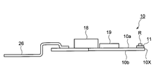
- FIG. 2 is a side view showing an example of the configuration of the first printed board 10 shown in FIG. 1 viewed from the side.
- FIG. 3 is a top view showing an example of the configuration of the second printed circuit board 20 used in the electronic apparatus 1 according to the first embodiment as viewed from above.
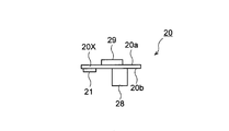
- FIG. 4 is a side view showing an example of the configuration of the second printed board 20 shown in FIG. 3 viewed from the side.
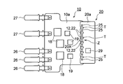
- FIG. 5 is a top view illustrating an example of a configuration in which two printed circuit boards bonded to the electronic device 1 according to the first embodiment are viewed from above.
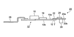
- FIG. 6 is a side view showing an example of a configuration in which two printed circuit boards bonded to the electronic device 1 shown in FIG. 5 are viewed from the side.
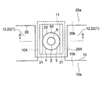
- FIG. 7A is a top view illustrating an example of a configuration in which a region Z in the vicinity of the joint portion of the electronic device 1 illustrated in FIG. 5 is enlarged.
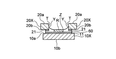
- FIG. 7B is a cross-sectional view showing an example of a cross section taken along line AA in the vicinity of the joint portion shown in FIG. 7A.
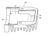
- FIG. 8 is a perspective view of the case 30 used in the electronic apparatus 1 according to the first embodiment.
- FIG. 9 is a cross-sectional view of the electronic device 1 according to the first embodiment.
- FIG. 10 is a cross-sectional view for explaining the method for manufacturing the electronic device 1 according to the first embodiment.
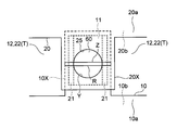
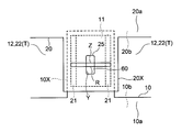
- FIG. 11 is a top view illustrating another example of the configuration in which the region Z in the vicinity of the joint portion of the electronic device 1 illustrated in FIG. 5 is enlarged.
- 12 is a top view showing another example of a configuration in which the region Z in the vicinity of the joint portion of the electronic device 1 shown in FIG. 5 is enlarged.
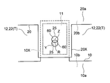
- FIG. 13 is a top view showing another example of the configuration in which the region Z in the vicinity of the joint portion of the electronic device 1 shown in FIG. 5 is enlarged.
- FIG. 14 is a top view illustrating another example of the configuration in which the region Z in the vicinity of the joint portion of the electronic device 1 illustrated in FIG. 5 is enlarged.
- FIG. 1 is a top view showing an example of a configuration of a first printed circuit board 10 used in the electronic apparatus 1 according to the first embodiment as viewed from above.
- FIG. 2 is a side view showing an example of the configuration of the first printed circuit board 10 shown in FIG. 1 viewed from the side.
- FIG. 3 is a top view showing an example of the configuration of the second printed circuit board 20 used in the electronic apparatus 1 according to the first embodiment as viewed from above.
- FIG. 4 is a side view showing an example of the configuration of the second printed board 20 shown in FIG. 3 viewed from the side.
- FIG. 5 is a top view showing an example of the configuration of the two printed circuit boards bonded to the electronic device 1 according to the first embodiment as viewed from above.
- FIG. 6 is a side view showing an example of a configuration in which two printed circuit boards bonded to the electronic device 1 shown in FIG. 5 are viewed from the side.
- FIG. 7A is a top view showing an example of an enlarged configuration of a region Z in the vicinity of the joint portion of the electronic device 1 shown in FIG.
- FIG. 7B is a cross-sectional view showing an example of a cross section taken along line AA in the vicinity of the joint shown in FIG. 7A.
- FIG. 8 is a perspective view of the case 30 used in the electronic apparatus 1 according to the first embodiment.
- FIG. 9 is a cross-sectional view of the electronic device 1 according to the first embodiment.
- FIG. 10 is a cross-sectional view for explaining the method for manufacturing the electronic device 1 according to the first embodiment.
- the printed circuit board 10 (first printed circuit board) and the printed circuit board 20 (second printed circuit board) used in the electronic apparatus 1 (FIGS. 9 and 10) according to the embodiment will be described.
- the electronic device 1 is, for example, a switching regulator (REG / RECT) that converts AC power output from an AC generator into DC power and outputs the DC power to a battery.
- a switching regulator REG / RECT
- the electronic device 1 includes a first printed board 10 (lower board), a second printed board 20 (upper board), and a conductive bonding material 60.
- the first printed circuit board 10 (lower substrate) includes a first main surface (upper surface) 10a and a second main surface 10a opposite to the first main surface 10a.
- the first printed circuit board 10 is provided with a first connection land portion 11 at a side end of the first main surface 10a, and a reference member R (resist) is provided on the first connection land portion 11. ing.
- the electronic component 18 is a diode constituting a diode bridge.
- the electronic component 19 is a semiconductor switch element (MOSFET, IGBT, etc.) that constitutes a power conversion circuit that converts AC power input from the AC generator into DC power.
- the first printed circuit board 10 is a board having excellent heat dissipation, such as an aluminum board or a ceramic board.
- the 1st printed circuit board 10 is not restricted to this, A glass epoxy board
- the second main surface 10b of the first printed circuit board 10 functions as a heat radiating surface for radiating heat generated from a heat generating component such as a diode or a semiconductor switch element. For this reason, no electronic component is mounted on the second main surface 10b.
- the first main surface 10 a is provided with a plurality of first connection land portions 11 along the side edges of the first printed circuit board 10.
- the 1st notch part 12 is formed in each area
- size and shape of the 1st notch part 12 are not specifically limited.
- the first connection land portion 11 is formed as a part of the wiring pattern formed on the first main surface 10a.
- the first printed circuit board 10 is provided with three bus bars 26 and two bus bars 27.
- the bus bar 26 is a terminal for inputting three-phase AC power generated by an AC generator (ACG).
- the two bus bars are terminals for outputting DC power obtained by power conversion.
- bus bars 26 and 27 are provided so as to extend outward from the side end opposite to the side end of the first printed circuit board 10 provided with the plurality of first connection land portions 11. ing.
- the second printed circuit board 20 (upper board) includes a third main surface (upper surface) 20a and a fourth main surface opposite to the third main surface 20a. And a surface (lower surface) 20b.
- the second printed circuit board 20 is formed with a substrate through-hole 25 penetrating between the third main surface 20a and the fourth main surface 20b at the side end of the fourth main surface 20b.
- a second connection land portion 21 is provided in the vicinity of the opening of the substrate through hole 25 on the surface 20b.
- an electronic component 29 is mounted on the third main surface 20a, and an electronic component 28 is mounted on the fourth main surface 20b.
- the electronic component 28 is a smoothing capacitor
- the electronic component 29 is a control IC for ON / OFF control of the semiconductor switch element.
- the second printed circuit board 20 is, for example, a glass epoxy board.
- the control IC By mounting the control IC on the glass epoxy substrate, it is possible to reduce the influence of noise compared to the case where the control IC is mounted on a metal substrate such as an aluminum substrate, and to suppress malfunctions and the like.
- a second connection land portion 21 is provided on the fourth main surface 20 b of the second printed circuit board 20. As shown in FIG. 4, the second connection land portion 21 is provided immediately below the substrate through hole 25. As described above, the fourth main surface 20 b of the second printed circuit board 20 is provided with a plurality of second connection land portions 21 (along the side edges of the second printed circuit board 20.
- the second connection land portion 21 is formed as a part of the wiring pattern formed on the fourth main surface 20b.
- the substrate through hole 25 electrically connects the second connection land portion 21 and the wiring pattern 23 formed on the third main surface 20a.
- the electronic component 19 and the electronic component 29 are electrically connected through the substrate through hole 25.
- the 2nd notch part 22 is each formed in each area
- the size and shape of the second notch 22 are not particularly limited.
- the second notch 22 is formed deeply until it intersects a straight line L that connects adjacent substrate through holes 25. Thereby, the curvature of the 2nd printed circuit board 20 at the time of a heating can further be suppressed.
- the first and second cutout portions 12 and 22 are not limited to the case where they are provided on both the first printed circuit board 10 and the second printed circuit board 20 as described above.
- the second printed board 20 may be provided only on one printed board.
- a notch is provided only on a printed circuit board having a larger linear expansion coefficient.
- a plurality of cutout portions are not limited to being provided, and only one cutout portion may be provided on the printed board. In this case, it is preferable to provide a notch at the center of the side edge of the printed circuit board.
- the first printed circuit board 10 (lower substrate) provided with the reference member R (resist) on the first connection land portion 11 is prepared (first step).
- the substrate through hole 25 penetrating between the main surface 20b and the second connecting land portion 21 is provided in the vicinity of the opening of the substrate through hole 25 of the fourth main surface 20b.
- a printed board 20 (upper board) is prepared (second step).
- first connection land portions 11 and the second connection land portions 21 are electrically conductive so that the first connection land portions 11 are electrically connected to the corresponding second connection land portions 21. Electrical connection is made with the bonding material 60 (third step (bonding step)).
- the first printed circuit board 10 and the second printed circuit board 20 have a side end of the first main surface 10a and a side end of the fourth main surface 20b.
- the first connection land portion 11 and the second connection land portion 21 are joined by the conductive bonding material 60 so as to be electrically connected, and the reference member R and the conductive bonding material 60 are used as a reference.
- a normal line that passes through the interface Z and is perpendicular to the first main surface 10 a passes through the inside of the substrate through hole 25.
- the conductive bonding material 60 is, for example, cream solder (solder material), and is applied onto the first connection land portion 11 before the bonding process.
- the conductive bonding material 60 may be a conductive bonding material that is cured by heating, and is not limited to solder.
- a conductive paste such as a silver paste may be used, or a conductive adhesive in which conductive nanoparticles are dispersed in an adhesive may be used.
- the electronic components 18, 19, 28, 29 and the bus bars 26, 27 are placed on cream solder applied to predetermined positions of the first and second printed circuit boards 10, 20, respectively, before the joining process. Is done.
- the notch 12 of the first printed circuit board 10 and the second printed circuit board 20 are provided.
- the first printed circuit board 10 and the second printed circuit board 20 may be joined so that at least a part of the cutout part 22 overlaps to form the through portion T.
- the through-hole T can function as a bubble escape hole.
- the electronic device 1 directly bonding printed circuit board in which the first printed circuit board 10 and the second printed circuit board 20 are directly bonded is provided. can get.
- the plurality of first connection land portions 11 and the reference member R are provided along the side end of the first main surface 10 a.
- a plurality of second connection land portions 21 are provided along the side end of the fourth main surface 20b.
- the conductive bonding material 60 is electrically connected between the first connection land portion 11 and the second connection land portion 21.
- first printed circuit board 10 and the second printed circuit board 20 are connected to each other in a state where the side end of the first main surface 10a and the side end of the fourth main surface 20b face each other.
- the first main member is joined by the conductive bonding material 60 so as to be electrically connected to the land portion 11 and the second connection land portion 21 and passes through the reference interface Z between the reference member R and the conductive bonding material 60.
- a normal line perpendicular to the surface 10 a passes through the substrate through-hole 25.
- At least a part of the conductive bonding material 60 is located between the end of the first connection land portion 11 and the second connection land portion 21.
- the reference member R is configured to repel the molten conductive bonding material (solder material) 60 when the first printed board 10 and the second printed board 20 are bonded.
- the reference member R is, for example, a resist containing resin.
- the normal line perpendicular to the first main surface 10a passing through the reference interface Z between the reference member R and the conductive bonding material 60 passes through the inside of the substrate through hole 25, whereby the reference member R
- the reference interface Z between the conductive bonding material 60 and the conductive bonding material 60 can be confirmed from the third main surface 20 a side of the substrate through-hole 25.
- the shape of the cross section parallel to the first main surface 10a of the reference member R may be, for example, a circle or a polygon (in the example of FIGS. 7A and 7B, it is a circle).
- the shape of the cross section of the substrate through hole 25 parallel to the fourth main surface 20b may be, for example, a circle or a polygon (in the example of FIGS. 7A and 7B, it is a circle).
- the vertical thickness of the reference member R is set to be smaller than the distance between the surface of the first connection land portion 11 and the surface of the second connection land portion 21.
- the electronic device 1 includes the conductive bonding material 60 and the first printed circuit board 10 and the second printed circuit board 20 that are directly bonded by the conductive bonding material 60.
- the first printed circuit board 10 and the second printed circuit board 20 are connected to the first main surface 10a of the first printed circuit board 10 and the second printed circuit board 10, as shown in FIGS. 5, 6, 7A, and 7B.
- the fourth main surface 20b of the printed circuit board 20 faces, and the plurality of first connection land parts 11 provided on the first printed circuit board 10 are electrically connected to the corresponding second connection land parts 21 respectively. As shown in FIG.
- first printed circuit board 10 and the second printed circuit board 20 have the first connection land portion in a state where the side end of the first main surface 10a and the side end of the fourth main surface 20b face each other. 11 and the second connecting land portion 21 are joined by the conductive bonding material 60 and pass through the reference interface Z between the reference member R and the conductive bonding material 60. A normal line perpendicular to the inside of the substrate through hole 25 penetrates.
- the electronic device 1 further includes a case 30 opened upward, a cover plate 40 of the case 30, and a sealing portion 50 filled in the case 30.
- a housing that houses the bus bars 26 and 27 may be provided.
- the case 30 has a bottom surface 31 (first bottom surface) and a bottom surface 32 (second bottom surface) deeper than the bottom surface 31, as shown in FIG.
- the bottom surface 31 and the bottom surface 32 are connected by a slope 33.
- an opening 34 for projecting the bus bars 26 and 27 from the case 30 is provided on the left side of the case 30, an opening 34 for projecting the bus bars 26 and 27 from the case 30 is provided.
- the material of the case 30 is preferably a material having high thermal conductivity, such as a metal such as aluminum.
- the cover plate 40 closes the opening above the case 30.
- the case 30 and the cover plate 40 define a storage space for storing the first and second printed circuit boards 10 and 20.
- the first printed circuit board 10 and the second printed circuit board 20 are accommodated in a case 30. More specifically, the first printed circuit board 10 is housed in the case 30 so that the second main surface 10b (heat radiating surface) is in contact with the bottom surface 31, and the second printed circuit board 20 is located above the bottom surface 32. It is stored in the case 30 so as to be positioned.
- the first printed circuit board 10 is housed in the case 30 so that the second main surface 10b (heat radiating surface) is in contact with the bottom surface 31, and the second printed circuit board 20 is located above the bottom surface 32. It is stored in the case 30 so as to be positioned.
- the cutout portion 12 of the first printed circuit board 10 and the cutout portion 22 of the second printed circuit board 20 at least partially overlap each other to form a through portion T.
- the through portion T communicates with a space S defined by the case 30 and the second printed circuit board 20.
- the penetration part T may be located above the slope 33 as shown in FIG.
- the penetrating portion T may be positioned above the slope 33.
- the boundary between the bottom surface 31 and the inclined surface 33 is exposed at the through portion T.
- the sealing part 50 is filled in a storage space defined by the case 30 and the cover plate 40.
- the sealing unit 50 seals the first and second printed circuit boards 10 and 20 accommodated in the case 30.
- the sealing part 50 consists of hard epoxy resins, for example.
- the sealing portion 50 is preferably made of a hard resin.
- the first printed circuit board 10 is directly bonded so that the lower surface (heat radiating surface) 10 b is in contact with the bottom surface 31 and the second printed circuit board 20 is positioned above the bottom surface 32.
- the first printed circuit board 10 and the second printed circuit board 20 are stored in the case 30 (storage process).
- the first printed circuit board 10 and the second printed circuit board 20 are accommodated in the case 30 so that the penetrating portion T communicates with the space S defined by the case 30 and the second printed circuit board 20.
- the opening above the case 30 is closed by the cover plate 40 (blocking step).
- the cover plate 40 is fixed to the case 30 with an adhesive or a screw so as to close the opening above the case 30.
- the case 30 is arranged so that the side opening 34 faces upward.
- sealing resin is injected into the storage space defined by the case 30 and the cover plate 40 from the opening 34 on the side surface of the case 30, and the first and second printed circuit boards 10 and 20 stored in the case 30 are attached. Sealing (sealing process).
- the through portion T is provided, the bubbles accumulated in the space S during the sealing step rise to the opening 34 through the through portion T. Therefore, bubbles can be suppressed from remaining in the space S.
- the electronic device 1 can be manufactured through the above steps.
- the electronic device device includes the first main surface and the second main surface opposite to the first main surface, and the first main surface side.
- a first printed circuit board (lower substrate) having a first connection land portion provided at an end thereof and a reference member (resist) provided on the first connection land portion; a third main surface;
- a substrate through hole penetrating between the third main surface and the fourth main surface is formed at a side end of the fourth main surface.
- a second printed circuit board (upper substrate) provided with a second connection land portion in the vicinity of the opening of the substrate through hole on the fourth main surface, the first connection land portion, and the second connection land portion And a conductive bonding material that electrically connects the two.
- the reference member repels the molten conductive bonding material when bonding the first printed board and the second printed board.
- the first printed circuit board and the second printed circuit board have the first connection land portion and the second printed circuit board in a state where the side end of the first main surface and the side end of the fourth main surface face each other.
- the normal line perpendicular to the first main surface that is bonded by the conductive bonding material so as to be electrically connected to the two connection land portions and passes through the reference interface between the reference member and the conductive bonding material is It penetrates the inside.
- the normal line perpendicular to the first main surface passing through the reference interface between the reference member (resist) and the conductive bonding material (solder material) passes through the inside of the substrate through hole.
- the reference interface with the conductive bonding material can be confirmed (confirmed with a microscope or the like) from the third main surface side of the substrate through hole.
- the reference interface between the reference member and the conductive bonding material it can be determined whether or not at least the first connection land portion (copper plate) and the conductive bonding material (solder material) are bonded.
- the reference interface cannot be confirmed, it is determined that the first connection land portion (copper plate) and the conductive bonding material (solder material) are not joined, and when the reference interface cannot be confirmed, 1 is determined that the connecting land portion (copper plate) and the conductive bonding material (solder material) are bonded. That is, it can be easily confirmed that the two printed boards are normally joined by soldering.
- the cross-sectional shape parallel to the first main surface 10a of the reference member R is circular, and the cross-sectional shape parallel to the fourth main surface 20b of the substrate through-hole 25 is circular.
- An example of the configuration has been described.
- the first shape can be obtained.
- the configuration shown in the embodiment may be different. Therefore, in the second embodiment, the shape of the cross section parallel to the first main surface 10a of the reference member R and the shape of the cross section parallel to the fourth main surface 20b of the substrate through hole 25 are different. An example will be described.
- FIG. 11 is a top view showing another example of the configuration in which the region Z in the vicinity of the joint portion of the electronic device 1 shown in FIG. 5 is enlarged.
- the same reference numerals as those in FIG. 7A indicate the same configurations as those in the first embodiment.
- the shape of the cross section parallel to the first main surface 10a of the reference member R is a rectangle, and the shape of the cross section parallel to the fourth main surface 20b of the substrate through-hole 25 is It is circular.
- the reference interface Z between the reference member R and the conductive bonding material 60 is a substrate. It can be seen from the third main surface 20a side of the through hole 25.
- the normal line perpendicular to the first main surface 10a passing through the reference interface Z between the reference member R and the conductive bonding material 60 passes through the inside of the substrate through hole 25, whereby the reference member R
- the reference interface Z between the conductive bonding material 60 and the conductive bonding material 60 can be confirmed from the third main surface 20 a side of the substrate through-hole 25.
- the two first and second printed circuit boards 10 and 20 can be easily joined normally by soldering. Can be confirmed.
- the shape of the cross section parallel to the first main surface 10a of the reference member R and still another example of the shape of the cross section parallel to the fourth main surface 20b of the substrate through hole 25 are described. explain.
- FIG. 12 is a top view showing another example of the configuration in which the region Z in the vicinity of the joint portion of the electronic device 1 shown in FIG. 5 is enlarged.
- the same reference numerals as those in FIG. 7A indicate the same configurations as those in the first embodiment.
- the shape of the cross section parallel to the first main surface 10a of the reference member R is a rectangle
- the shape of the cross section parallel to the fourth main surface 20b of the substrate through hole 25 is It is a rectangle.
- the longitudinal direction of the rectangular reference member R and the longitudinal direction of the rectangular substrate through hole 25 are orthogonal to each other.
- the reference interface Z between the reference member R and the conductive bonding material 60 is the substrate. It can be seen from the third main surface 20a side of the through hole 25.
- the fourth main surface of the conductive bonding material 60 and the substrate through-hole 25 is used. There will be a fillet interface Y in contact with the opening on the 20b side.
- the normal line perpendicular to the first main surface 10a passing through the reference interface Z between the reference member R and the conductive bonding material 60 passes through the inside of the substrate through hole 25, whereby the reference member R
- the reference interface Z between the conductive bonding material 60 and the conductive bonding material 60 can be confirmed from the third main surface 20 a side of the substrate through-hole 25.
- the two first and second printed boards 10 and 20 can be easily joined normally by soldering. Can be confirmed.
- the shape of the cross section parallel to the first main surface 10a of the reference member R and the other example of the shape of the cross section parallel to the fourth main surface 20b of the substrate through hole 25 are described. explain.
- FIG. 13 is a top view illustrating another example of the configuration in which the region Z in the vicinity of the joint portion of the electronic device 1 illustrated in FIG. 5 is enlarged.
- the same reference numerals as those in FIG. 7A indicate the same configurations as those in the first embodiment.
- the shape of the cross section parallel to the first main surface 10a of the reference member R is a rectangle
- the shape of the cross section parallel to the fourth main surface 20b of the substrate through-hole 25 is It is a shape in which two circular parts are connected.
- the reference interface Z between the reference member R and the conductive bonding material 60 is the substrate. It can be seen from the third main surface 20a side of the through hole 25.
- the normal line perpendicular to the first main surface 10a passing through the reference interface Z between the reference member R and the conductive bonding material 60 passes through the inside of the substrate through hole 25, whereby the reference member R
- the reference interface Z between the conductive bonding material 60 and the conductive bonding material 60 can be confirmed from the third main surface 20 a side of the substrate through-hole 25.
- the two first and second printed boards 10 and 20 can be easily joined normally by soldering. Can be confirmed.
- the shape of the cross section parallel to the first main surface 10a of the reference member R and the other example of the shape of the cross section parallel to the fourth main surface 20b of the substrate through hole 25 are described. explain.
- FIG. 14 is a top view showing another example of the configuration in which the region Z in the vicinity of the joint portion of the electronic device 1 shown in FIG. 5 is enlarged.
- the same reference numerals as those in FIG. 7A indicate the same configurations as those in the first embodiment.
- the shape of the cross section parallel to the first main surface 10a of the reference member R is a rectangle, and the shape of the cross section parallel to the fourth main surface 20b of the substrate through-hole 25 is It is circular.
- the reference interface Z between the reference member R and the conductive bonding material 60 is a substrate. It can be seen from the third main surface 20a side of the through hole 25.
- the normal line perpendicular to the first main surface 10a passing through the reference interface Z between the reference member R and the conductive bonding material 60 passes through the inside of the substrate through hole 25, whereby the reference member R
- the reference interface Z between the conductive bonding material 60 and the conductive bonding material 60 can be confirmed from the third main surface 20 a side of the substrate through-hole 25.
- the two first and second printed boards 10 and 20 can be easily joined normally by soldering. Can be confirmed.
Landscapes
- Engineering & Computer Science (AREA)
- Microelectronics & Electronic Packaging (AREA)
- Manufacturing & Machinery (AREA)
- Combinations Of Printed Boards (AREA)
- Electric Connection Of Electric Components To Printed Circuits (AREA)
Abstract
電子装置は、第1の主面と、第1の主面と反対側の第2の主面とを有し、第1の主面の側端に第1の接続ランド部が設けられ、第1の接続ランド部上に基準部材が設けられた第1のプリント基板と、第3の主面と、第3の主面と反対側の第4の主面とを有し、第4の主面の側端に第3の主面と第4の主面との間を貫通する基板貫通孔が形成され、第4の主面の基板貫通孔の開口部に近接して第2の接続ランド部が設けられた第2のプリント基板と、第1の接続ランド部と第2の接続ランド部との間を電気的に接続する導電性接合材と、を備える。基準部材は、第1のプリント基板と第2のプリント基板とを接合する際に溶融した導電性接合材をはじくようになっている。
Description
本発明は、電子装置の製造方法に関する発明である。
従来、例えば、半導体スイッチ素子を制御する制御ICを、半導体スイッチ素子やダイオード等の発熱部品が実装されるプリント基板とは別のプリント基板に実装することが行われている。
そして、例えば、特開平11-103145号公報には、2枚のプリント基板がはんだで直接接合された回路基板が記載されている。
上述のように、プリント基板同士を、はんだ(導電性接合材)で直接接合する場合、はんだ接合部が基板で隠れるため、リフロー工程後に、はんだ付けが正常に行われたかどうかを確認することが困難となる問題がある。
そこで、本発明は、2枚のプリント基板がはんだ付けにより正常に接合されていることを容易に確認することが可能なプリント基板の接合方法、電子装置、および電子装置の製造方法を提供することを目的とする。
本発明の一態様に係る実施形態に従った電子装置は、
第1の主面と、前記第1の主面と反対側の第2の主面とを有し、前記第1の主面の側端に第1の接続ランド部が設けられ、前記第1の接続ランド部上に基準部材が設けられた第1のプリント基板と、
第3の主面と、前記第3の主面と反対側の第4の主面とを有し、前記第4の主面の側端に前記第3の主面と前記第4の主面との間を貫通する基板貫通孔が形成され、前記第4の主面の基板貫通孔の開口部に近接して第2の接続ランド部が設けられた第2のプリント基板と、
前記第1の接続ランド部と前記第2の接続ランド部との間を電気的に接続する導電性接合材と、を備え、
前記基準部材は、前記第1のプリント基板と前記第2のプリント基板とを接合する際に溶融した前記導電性接合材をはじくようになっている
ことを特徴とする。
第1の主面と、前記第1の主面と反対側の第2の主面とを有し、前記第1の主面の側端に第1の接続ランド部が設けられ、前記第1の接続ランド部上に基準部材が設けられた第1のプリント基板と、
第3の主面と、前記第3の主面と反対側の第4の主面とを有し、前記第4の主面の側端に前記第3の主面と前記第4の主面との間を貫通する基板貫通孔が形成され、前記第4の主面の基板貫通孔の開口部に近接して第2の接続ランド部が設けられた第2のプリント基板と、
前記第1の接続ランド部と前記第2の接続ランド部との間を電気的に接続する導電性接合材と、を備え、
前記基準部材は、前記第1のプリント基板と前記第2のプリント基板とを接合する際に溶融した前記導電性接合材をはじくようになっている
ことを特徴とする。
前記電子装置において、
前記第1のプリント基板と前記第2のプリント基板とは、前記第1の主面の前記側端と前記第4の主面の前記側端とが対向した状態で、前記第1の接続ランド部と前記第2の接続ランド部と電気的に接続されるように前記導電性接合材により接合され且つ前記基準部材と前記導電性接合材との基準界面を通る前記第1の主面に垂直な法線が前記基板貫通孔の内部を貫通している
ことを特徴とする。
前記第1のプリント基板と前記第2のプリント基板とは、前記第1の主面の前記側端と前記第4の主面の前記側端とが対向した状態で、前記第1の接続ランド部と前記第2の接続ランド部と電気的に接続されるように前記導電性接合材により接合され且つ前記基準部材と前記導電性接合材との基準界面を通る前記第1の主面に垂直な法線が前記基板貫通孔の内部を貫通している
ことを特徴とする。
前記電子装置において、
前記基準部材と前記導電性接合材との前記基準界面が前記基板貫通孔の前記第3の主面側から見えている
ことを特徴とする。
前記基準部材と前記導電性接合材との前記基準界面が前記基板貫通孔の前記第3の主面側から見えている
ことを特徴とする。
前記電子装置において、
前記導電性接合材と前記基板貫通孔の前記第4の主面側の開口部とが接触するフィレット界面が存在している
ことを特徴とする。
前記導電性接合材と前記基板貫通孔の前記第4の主面側の開口部とが接触するフィレット界面が存在している
ことを特徴とする。
前記電子装置において、
前記第1の接続ランド部の端部と前記第2の接続ランド部との間に前記導電性接合材の少なくとも一部が位置していることを特徴とする。
前記第1の接続ランド部の端部と前記第2の接続ランド部との間に前記導電性接合材の少なくとも一部が位置していることを特徴とする。
前記電子装置において、
前記基準部材は、樹脂を含むレジストであることを特徴とする。
前記基準部材は、樹脂を含むレジストであることを特徴とする。
前記電子装置において、
前記導電性接合材は、はんだ材であることを特徴とする。
前記導電性接合材は、はんだ材であることを特徴とする。
前記電子装置において、
前記基準部材の厚さは、前記第1の接続ランド部の表面と前記第2の接続ランド部の表面との間の距離よりも小さいことを特徴とする。
前記基準部材の厚さは、前記第1の接続ランド部の表面と前記第2の接続ランド部の表面との間の距離よりも小さいことを特徴とする。
前記電子装置において、
前記第1の主面の前記側端に沿って複数の前記第1の接続ランド部及び基準部材が設けられ、前記第1の接続ランド部及び基準部材に対応して、前記第4の主面の前記側端に沿って複数の前記第2の接続ランド部が設けられている
ことを特徴とする。
前記第1の主面の前記側端に沿って複数の前記第1の接続ランド部及び基準部材が設けられ、前記第1の接続ランド部及び基準部材に対応して、前記第4の主面の前記側端に沿って複数の前記第2の接続ランド部が設けられている
ことを特徴とする。
前記電子装置において、
前記基準部材の前記第1の主面に平行な断面の形状は、円形、又は、多角形であることを特徴とする。
前記基準部材の前記第1の主面に平行な断面の形状は、円形、又は、多角形であることを特徴とする。
前記電子装置において、
前記基板貫通孔の前記第4の主面に平行な断面の形状は、円形、又は、多角形であることを特徴とする。
前記基板貫通孔の前記第4の主面に平行な断面の形状は、円形、又は、多角形であることを特徴とする。
前記電子装置において、
前記基準部材が長方形の形状を有する場合に、前記長方形の前記基準部材の長手方向と、前記長方形の基板貫通孔の長手方向とが直交することを特徴とする。
前記基準部材が長方形の形状を有する場合に、前記長方形の前記基準部材の長手方向と、前記長方形の基板貫通孔の長手方向とが直交することを特徴とする。
前記電子装置において、
前記第1のプリント基板の隣接する前記第1の接続ランド部間の領域には、第1の切り欠き部が形成され、前記第2のプリント基板の隣接する隣接する第2の接続ランド部間の領域には、第2の切り欠き部が形成されていることを特徴とする。
前記第1のプリント基板の隣接する前記第1の接続ランド部間の領域には、第1の切り欠き部が形成され、前記第2のプリント基板の隣接する隣接する第2の接続ランド部間の領域には、第2の切り欠き部が形成されていることを特徴とする。
前記電子装置において、
前記第1のプリント基板は、アルミニウム基板またはセラミック基板であり、前記第2のプリント基板は、ガラスエポキシ基板であることを特徴とする。
前記第1のプリント基板は、アルミニウム基板またはセラミック基板であり、前記第2のプリント基板は、ガラスエポキシ基板であることを特徴とする。
本発明の一態様に係る実施形態に従った電子装置の製造方は、
2枚のプリント基板を接合する電子装置の製造方法であって、
第1の主面と、前記第1の主面と反対側の第2の主面とを有し、前記第1の主面の側端に第1の接続ランド部が設けられ、前記第1の接続ランド部上に基準部材が設けられた第1のプリント基板を準備する第1の工程と、
第3の主面と、前記第3の主面と反対側の第4の主面とを有し、前記第4の主面の側端に前記第3の主面と前記第4の主面との間を貫通する基板貫通孔が形成され、前記第4の主面の基板貫通孔の開口部に近接して第2の接続ランド部が設けられた第2のプリント基板を準備する第2の工程と、
前記第1の接続ランド部と前記第2の接続ランド部との間を導電性接合材で電気的に接続する第3の工程と、を備え、
前記基準部材は、前記第1のプリント基板と前記第2のプリント基板とを接合する際に溶融した前記導電性接合材をはじくようになっており、
前記第3の工程において、前記第1のプリント基板と前記第2のプリント基板とは、前記第1の主面の前記側端と前記第4の主面の前記側端とが対向した状態で、前記第1の接続ランド部と前記第2の接続ランド部と電気的に接続されるように前記導電性接合材により接合され且つ前記基準部材と前記導電性接合材との基準界面を通る前記第1の主面に垂直な法線が前記基板貫通孔の内部を貫通している
ことを特徴とする。
2枚のプリント基板を接合する電子装置の製造方法であって、
第1の主面と、前記第1の主面と反対側の第2の主面とを有し、前記第1の主面の側端に第1の接続ランド部が設けられ、前記第1の接続ランド部上に基準部材が設けられた第1のプリント基板を準備する第1の工程と、
第3の主面と、前記第3の主面と反対側の第4の主面とを有し、前記第4の主面の側端に前記第3の主面と前記第4の主面との間を貫通する基板貫通孔が形成され、前記第4の主面の基板貫通孔の開口部に近接して第2の接続ランド部が設けられた第2のプリント基板を準備する第2の工程と、
前記第1の接続ランド部と前記第2の接続ランド部との間を導電性接合材で電気的に接続する第3の工程と、を備え、
前記基準部材は、前記第1のプリント基板と前記第2のプリント基板とを接合する際に溶融した前記導電性接合材をはじくようになっており、
前記第3の工程において、前記第1のプリント基板と前記第2のプリント基板とは、前記第1の主面の前記側端と前記第4の主面の前記側端とが対向した状態で、前記第1の接続ランド部と前記第2の接続ランド部と電気的に接続されるように前記導電性接合材により接合され且つ前記基準部材と前記導電性接合材との基準界面を通る前記第1の主面に垂直な法線が前記基板貫通孔の内部を貫通している
ことを特徴とする。
本発明の一態様に係る電子機器装置は、第1の主面と、第1の主面と反対側の第2の主面とを有し、第1の主面の側端に第1の接続ランド部が設けられ、第1の接続ランド部上に基準部材が設けられた第1のプリント基板と、第3の主面と、第3の主面と反対側の第4の主面とを有し、第4の主面の側端に第3の主面と第4の主面との間を貫通する基板貫通孔が形成され、第4の主面の基板貫通孔の開口部に近接して第2の接続ランド部が設けられた第2のプリント基板と、第1の接続ランド部と第2の接続ランド部との間を電気的に接続する導電性接合材と、を備える。
そして、基準部材は、第1のプリント基板と第2のプリント基板とを接合する際に溶融した導電性接合材をはじくようになっている。
そして、例えば、第1のプリント基板と第2のプリント基板とは、第1の主面の側端と第4の主面の側端とが対向した状態で、第1の接続ランド部と第2の接続ランド部と電気的に接続されるように導電性接合材により接合され且つ基準部材と導電性接合材との基準界面を通る第1の主面に垂直な法線が基板貫通孔の内部を貫通している。
これにより、基準部材と導電性接合材との基準界面を通る第1の主面に垂直な法線が基板貫通孔の内部を貫通していることにより、基準部材と導電性接合材との基準界面が基板貫通孔の第3の主面側から確認することができる。
このように基準部材と導電性接合材との基準界面を確認することにより、少なくとも第1の接続ランド部と導電性接合材とが接合されているか否かを判断できる。
すなわち、2枚のプリント基板がはんだ付けにより正常に接合されていることを容易に確認することができる。
以下、本発明に係る実施形態について図面に基づいて説明する。
図1は、第1の実施形態に係る電子装置1で用いられる第1のプリント基板10を上方から見た構成の一例を示す上面図である。また、図2は、図1に示す第1のプリント基板10を側方から見た構成の一例を示す側面図である。また、図3は、第1の実施形態に係る電子装置1で用いられる第2のプリント基板20を上方から見た構成の一例を示す上面図である。また、図4は、図3に示す第2のプリント基板20を側方から見た構成の一例を示す側面図である。また、図5は、第1の実施形態に係る電子装置1の接合された2枚のプリント基板を上方から見た構成の一例を示す上面図である。また、図6は、図5に示す電子装置1の接合された2枚のプリント基板を側方から見た構成の一例を示す側面図である。また、図7Aは、図5に示す電子装置1の接合部分近傍の領域Zを拡大した構成の一例を示す上面図である。また、図7Bは、図7Aに示す接合部分近傍のA-A線に沿った断面の一例を示す断面図である。また、図8は、第1の実施形態に係る電子装置1に用いられるケース30の斜視図である。また、図9は、第1の実施形態に係る電子装置1の断面図である。また、図10は、第1の実施形態に係る電子装置1の製造方法を説明するための断面図である。
まず、実施形態に係る電子装置1(図9、図10)で用いられるプリント基板10(第1のプリント基板)およびプリント基板20(第2のプリント基板)について説明する。
なお、電子装置1は、例えば、交流発電機から出力される交流電力を直流電力に変換してバッテリーに出力するスイッチングレギュレータ(REG/RECT)である。
この電子装置1は、第1のプリント基板10(下側基板)と、第2のプリント基板20(上側基板)と、導電性接合材60と、を備える。
ここで、この第1のプリント基板10(下側基板)は、図1、図2に示すように、第1の主面(上面)10aと、第1の主面10aと反対側の第2の主面(下面)10bとを有する。そして、この第1のプリント基板10は、第1の主面10aの側端に第1の接続ランド部11が設けられ、第1の接続ランド部11上に基準部材R(レジスト)が設けられている。
また、例えば、図1、図2に示すように、第1の主面10aには、電子部品18、19が実装されている。この電子部品18は、ダイオードブリッジを構成するダイオードである。電子部品19は、交流発電機から入力された交流電力を直流電力に変換する電力変換回路を構成する半導体スイッチ素子(MOSFET、IGBT等)である。
また、第1のプリント基板10は、例えば、アルミニウム基板またはセラミック基板等の放熱性に優れた基板である。ただし、第1のプリント基板10は、これに限られず、ガラスエポキシ基板等であってもよい。
なお、本実施形態では、第1のプリント基板10の第2の主面10bは、ダイオードや半導体スイッチ素子等の発熱部品から発せられた熱を放熱するための放熱面として機能する。このため、第2の主面10bには電子部品が実装されていない。
また、図1および図2に示すように、第1の主面10aには、第1のプリント基板10の側端に沿って複数の第1の接続ランド部11が設けられている。
そして、図1に示すように、第1のプリント基板10の隣接する第1の接続ランド部11間の各領域には、第1の切り欠き部12がそれぞれ形成されている。なお、第1の切り欠き部12の大きさや形状は特に限定されるものではない。
なお、第1の接続ランド部11は、第1の主面10aに形成された配線パターンの一部として形成されている。
なお、図1、図2に示すように、第1のプリント基板10には、3本のバスバー26および2本のバスバー27が設けられている。バスバー26は、交流発電機(ACG)により発生した三相交流電力を入力するための端子である。2本のバスバーは、電力変換により得られた直流電力を出力するための端子である。
本実施形態では、バスバー26、27は、複数の第1の接続ランド部11が設けられた第1のプリント基板10の側端とは反対側の側端から外側に延在するように設けられている。
また、第2のプリント基板20(上側基板)は、図3、図4に示すように、第3の主面(上面)20aと、前記第3の主面20aと反対側の第4の主面(下面)20bとを有する。
この第2のプリント基板20は、第4の主面20bの側端に第3の主面20aと第4の主面20bとの間を貫通する基板貫通孔25が形成され、第4の主面20bの基板貫通孔25の開口部に近接して第2の接続ランド部21が設けられている。
また、例えば、図3、図4に示すように、第3の主面20aには、電子部品29が実装され、第4の主面20bには、電子部品28が実装されている。この電子部品28は平滑コンデンサであり、電子部品29は半導体スイッチ素子をオン/オフ制御するための制御ICである。
また、第2のプリント基板20は、例えばガラスエポキシ基板である。ガラスエポキシ基板に制御ICを実装することにより、アルミニウム基板等の金属基板に制御ICを実装する場合に比べてノイズによる影響を軽減することができ、誤動作等を抑制することができる。
また、図3および図4に示すように、第2のプリント基板20の第4の主面20bには、第2の接続ランド部21が設けられている。この第2の接続ランド部21は、図4に示すように、基板貫通孔25の直下に設けられている。このように、第2のプリント基板20の第4の主面20bには、第2のプリント基板20の側端に沿って複数の第2の接続ランド部21(が設けられている。
なお、本実施形態では、第2の接続ランド部21は、第4の主面20bに形成された配線パターンの一部として形成されている。
また、基板貫通孔25は、第2の接続ランド部21と、第3の主面20aに形成された配線パターン23とを電気的に接続する。この基板貫通孔25を介して電子部品19と電子部品29とが電気的に接続されている。
そして、図3に示すように、第2のプリント基板20の隣接する隣接する第2の接続ランド部21(基板貫通孔25)間の各領域には、第2の切り欠き部22がそれぞれ形成されている。
なお、この第2の切り欠き部22の大きさや形状は特に限定されるものではない。例えば、第2の切り欠き部22は、図3に示すように、隣り合う基板貫通孔25同士を結ぶ直線Lと交差するまで深く形成されている。これにより、加熱時における第2のプリント基板20の反りをさらに抑制することができる。
なお、既述の第1、第2の切り欠き部12、22が設けられていることで、導電性接合材60のブリッジ(例えば、はんだブリッジ)が発生していないかどうかを作業者が目視で容易に確認することができる。
なお、第1、第2の切り欠き部12、22は、上記のように第1のプリント基板10および第2のプリント基板20の両方に設けられる場合に限られず、第1のプリント基板10および第2のプリント基板20のうち一方のプリント基板にのみ設けられてもよい。
例えば、線膨張率が大きい方のプリント基板にのみ切り欠き部を設ける。また、切り欠き部は、複数設けられる場合に限らず、プリント基板に1つだけ設けられてもよい。この場合、プリント基板の側端の中央部分に切り欠き部を設けることが好ましい。
ここで、上述の2枚のプリント基板(第1のプリント基板10および第2のプリント基板20)を接合する電子装置1の製造方法の一例について説明する。
まず、第1の主面10aと、第1の主面10aと反対側の第2の主面10bとを有し、第1の主面10aの側端に第1の接続ランド部11が設けられ、第1の接続ランド部11上に基準部材R(レジスト)が設けられた第1のプリント基板10(下側基板)を準備する(第1の工程)。
さらに、第3の主面20aと、第3の主面20aと反対側の第4の主面20bとを有し、第4の主面20bの側端に第3の主面20aと第4の主面20bとの間を貫通する基板貫通孔25が形成され、第4の主面20bの基板貫通孔25の開口部に近接して第2の接続ランド部21が設けられた第2のプリント基板20(上側基板)を準備する(第2の工程)。
そして、図5、図6、図7A、図7Bに示すように、第1のプリント基板10の第1の主面10aと第2のプリント基板20の第4の主面20bを対向させ、複数の第1の接続ランド部11がそれぞれ対応する第2の接続ランド部21に電気的に接続されるように、第1の接続ランド部11と第2の接続ランド部21との間を導電性接合材60で電気的に接続する(第3の工程(接合工程))。
なお、上記第3の工程(接合工程)において、第1のプリント基板10と第2のプリント基板20とは、第1の主面10aの側端と第4の主面20bの側端とが対向した状態で、第1の接続ランド部11と第2の接続ランド部21と電気的に接続されるように導電性接合材60により接合され且つ基準部材Rと導電性接合材60との基準界面Zを通る第1の主面10aに垂直な法線が基板貫通孔25の内部を貫通している。
なお、既述の第1、第2の工程の順序は、逆であってもよく、第1、第2の工程が同時に実施されてもよい。
なお、導電性接合材60は、例えば、クリームはんだ(はんだ材)であり、接合工程前に第1の接続ランド部11上に塗布される。
なお、導電性接合材60は、加熱により硬化する導電性の接合材であればよく、はんだに限定されない。例えば、銀ペーストなどの導電ペーストでもよいし、あるいは、導電性のナノ粒子を接着剤中に分散させた導電性接着剤でもよい。
なお、電子部品18、19、28、29およびバスバー26、27は、接合工程前において、各々、第1、第2のプリント基板10、20の所定の位置に塗布されたクリームはんだ上に載置される。
なお、既述の第3の工程(接合工程)において、図5、図6、図7A、図7Bに示すように、第1のプリント基板10の切り欠き部12と、第2のプリント基板20の切り欠き部22とは、少なくとも一部分が重なって貫通部Tを形成するように、第1のプリント基板10および第2のプリント基板20が接合されてもよい。
これにより、導電性接合材60が接続ランド部間を跨ぐこと(例えば、はんだブリッジ)を抑制できる。また、詳しくは電子装置1の製造方法で述べるが、第1のプリント基板10および第2のプリント基板20を樹脂封止する際に、貫通部Tを気泡逃し孔として機能させることができる。
上記のようにして、図5、図6、図7A、図7Bに示すように、第1のプリント基板10と第2のプリント基板20が直接接合された電子装置1(直接接合プリント基板)が得られる。
ここで、既述の図5、図6、図7A、図7Bに示すように、第1の主面10aの側端に沿って複数の第1の接続ランド部11及び基準部材Rが設けられ、第1の接続ランド部11及び基準部材Rに対応して、第4の主面20bの側端に沿って複数の第2の接続ランド部21が設けられている。
そして、図7A、図7Bに示すように、導電性接合材60は、第1の接続ランド部11と第2の接続ランド部21との間を電気的に接続している。
より詳しくは、第1のプリント基板10と第2のプリント基板20とは、第1の主面10aの側端と第4の主面20bの側端とが対向した状態で、第1の接続ランド部11と前記第2の接続ランド部21と電気的に接続されるように導電性接合材60により接合され且つ基準部材Rと導電性接合材60との基準界面Zを通る第1の主面10aに垂直な法線が基板貫通孔25の内部を貫通している。
特に、図7A、図7Bに示すように、第1の接続ランド部11の端部と第2の接続ランド部21との間に導電性接合材60の少なくとも一部が位置している。
なお、基準部材Rは、第1のプリント基板10と第2のプリント基板20とを接合する際に溶融した導電性接合材(はんだ材)60をはじくようになっている。この基準部材Rは、例えば、樹脂を含むレジストである。
また、図7A、図7Bに示すように、導電性接合材60と第1の接続ランド部11とが適切に接合されている場合には、基準部材Rと導電性接合材60との基準界面Zが基板貫通孔25の第3の主面20a側から見えている。
言い換えれば、例えば、電子装置1の製造工程における外観検査において、基準部材Rと導電性接合材60との基準界面Zが基板貫通孔25の第3の主面20a側から見えている場合には、導電性接合材60と第1の接続ランド部11とが適切に接合されていると判断することができる。
そして、図7A、図7Bに示すように、導電性接合材60と第2の接続ランド部21とが適切に接合されている場合には、導電性接合材60と基板貫通孔25の第4の主面20b側の開口部とが接触するフィレット界面Yが存在することとなる。
言い換えれば、例えば、電子装置1の製造工程における外観検査において、導電性接合材60と基板貫通孔25の第4の主面20b側の開口部とが接触するフィレット界面Yが存在する場合には、導電性接合材60と第2の接続ランド部21とが適切に接合されていると判断することができる。
上述のように、基準部材Rと導電性接合材60との基準界面Zを通る第1の主面10aに垂直な法線が基板貫通孔25の内部を貫通していることにより、基準部材Rと導電性接合材60との基準界面Zが基板貫通孔25の第3の主面20a側から確認することができる。
このように基準部材Rと導電性接合材60との基準界面Zを確認することにより、少なくとも第1の接続ランド部11と導電性接合材60とが接合されているか否かを判断できる。
すなわち、2枚の第1、第2のプリント基板10、20がはんだ付けにより正常に接合されていることを容易に確認することができる。
なお、基準部材Rの第1の主面10aに平行な断面の形状は、例えば、円形、又は、多角形であってもよい(図7A、図7Bの例では円形である)。
また、基板貫通孔25の第4の主面20bに平行な断面の形状は、例えば、円形、又は、多角形であってもよい(図7A、図7Bの例では円形である)。
また、基準部材Rの上下方向の厚さは、第1の接続ランド部11の表面と第2の接続ランド部21の表面との間の距離よりも小さくなるように設定されている。
次に、以上のような接合された第1、第2のプリント基板10、20を有する実施形態に係る電子装置1について説明する。
既述のように、電子装置1は、導電性接合材60と、この導電性接合材60により直接接合された第1のプリント基板10および第2のプリント基板20とを有している。
そして、第1のプリント基板10と第2のプリント基板20は、図5、図6、図7A、図7Bに示すように、第1のプリント基板10の第1の主面10aと第2のプリント基板20の第4の主面20bが対向し、第1のプリント基板10に設けられた複数の第1の接続ランド部11がそれぞれ対応する第2の接続ランド部21に電気的に接続されるように導電性接合材60により接合されている。
特に、第1のプリント基板10と第2のプリント基板20とは、第1の主面10aの側端と第4の主面20bの側端とが対向した状態で、第1の接続ランド部11と前記第2の接続ランド部21と電気的に接続されるように導電性接合材60により接合され且つ基準部材Rと導電性接合材60との基準界面Zを通る第1の主面10aに垂直な法線が基板貫通孔25の内部を貫通している。
そして、電子装置1は、図9に示すように、上方に開口したケース30と、ケース30のカバー板40と、ケース30内に充填された封止部50とをさらに有している。なお、図9では図示していないが、バスバー26、27を収納するハウジング(ソケット)が設けられてもよい。
また、ケース30は、図8に示すように、底面31(第1の底面)と、底面31より深い底面32(第2の底面)とを有する。底面31と底面32は、斜面33によって接続されている。ケース30の左側には、バスバー26、27をケース30から突出させるための開口34が設けられている。なお、ケース30の材質は、熱伝導性の高い材料が好ましく、例えば、アルミニウム等の金属である。
そして、カバー板40は、ケース30の上方の開口を閉塞する。ケース30とカバー板40により、第1、第2のプリント基板10、20を収納する収納空間が画成される。
そして、図9に示すように、第1のプリント基板10および第2のプリント基板20はケース30に収納されている。より詳しくは、第1のプリント基板10は、第2の主面10b(放熱面)が底面31に接するようにケース30に収納されており、第2のプリント基板20は、底面32の上方に位置するようにケース30に収納されている。
また、図9に示すように、第1のプリント基板10の切り欠き部12と、第2のプリント基板20の切り欠き部22とは、少なくとも一部分が重なって貫通部Tを構成している。この貫通部Tは、ケース30および第2のプリント基板20により画成される空間Sに連通している。
なお、貫通部Tは、図9に示すように、斜面33の上方に位置してもよい。
これにより、第1のプリント基板10および第2のプリント基板20を樹脂封止する際に、貫通部Tを介して空間Sに溜まった気泡を第1、第2のプリント基板10、20の上面側に逃し易くすることができる。
なお、貫通部Tの一部分のみが斜面33の上方に位置してもよい。また、好ましくは、底面31と斜面33の境界が貫通部Tに露出する。
封止部50は、ケース30とカバー板40により画成される収納空間に充填されている。この封止部50は、ケース30に収容された第1、第2のプリント基板10、20を封止する。
なお、封止部50は、例えば硬質エポキシ樹脂からなる。導電性接合材60のクラック(はんだクラック等)発生を防止するため、封止部50は硬質樹脂からなることが好ましい。
次に、以上のような構成を有する電子装置1の製造方法について詳しく説明する。
まず、上記の接合方法により導電性接合材60で直接接合された2枚の第1、第2のプリント基板10、20と、ケース30とを準備する。
次に、図9に示すように、第1のプリント基板10の下面(放熱面)10bが底面31に接し、かつ第2のプリント基板20が底面32の上方に位置するように、直接接合された第1のプリント基板10および第2のプリント基板20をケース30に収納する(収納工程)。本工程において、貫通部Tがケース30および第2のプリント基板20により画成される空間Sに連通するように、第1のプリント基板10および第2のプリント基板20をケース30に収納する。
次に、カバー板40によりケース30の上方の開口を閉塞する(閉塞工程)。具体的には、ケース30の上方の開口を閉塞するようにカバー板40を、接着剤あるいはネジ等によりケース30に固定する。
次に、図10に示すように、ケース30を側面の開口34が上方を向くように配置する。そして、ケース30とカバー板40により画成される収納空間に、ケース30の側面の開口34から封止樹脂を注入し、ケース30に収容された第1、第2のプリント基板10、20を封止する(封止工程)。本工程では、貫通部Tが設けられているため、封止工程の途中で空間Sに溜まった気泡は貫通部Tを通って開口34まで上昇していく。したがって、空間Sに気泡が残留することを抑制することができる。上記の工程を経て電子装置1を製造することができる。
以上のように、本発明の一態様に係る電子機器装置は、第1の主面と、第1の主面と反対側の第2の主面とを有し、第1の主面の側端に第1の接続ランド部が設けられ、第1の接続ランド部上に基準部材(レジスト)が設けられた第1のプリント基板(下側基板)と、第3の主面と、第3の主面と反対側の第4の主面とを有し、第4の主面の側端に第3の主面と第4の主面との間を貫通する基板貫通孔が形成され、第4の主面の基板貫通孔の開口部に近接して第2の接続ランド部が設けられた第2のプリント基板(上側基板)と、第1の接続ランド部と第2の接続ランド部との間を電気的に接続する導電性接合材と、を備える。
そして、基準部材は、第1のプリント基板と第2のプリント基板とを接合する際に溶融した導電性接合材をはじくようになっている。
そして、例えば、第1のプリント基板と第2のプリント基板とは、第1の主面の側端と第4の主面の側端とが対向した状態で、第1の接続ランド部と第2の接続ランド部と電気的に接続されるように導電性接合材により接合され且つ基準部材と導電性接合材との基準界面を通る第1の主面に垂直な法線が基板貫通孔の内部を貫通している。
これにより、基準部材(レジスト)と導電性接合材(はんだ材)との基準界面を通る第1の主面に垂直な法線が基板貫通孔の内部を貫通していることにより、基準部材と導電性接合材との基準界面が基板貫通孔の第3の主面側から確認(顕微鏡等で確認)することができる。
このように基準部材と導電性接合材との基準界面を確認することにより、少なくとも第1の接続ランド部(銅版)と導電性接合材(はんだ材)とが接合されているか否かを判断できる(例えば、当該基準界面が確認できない場合は、第1の接続ランド部(銅版)と導電性接合材(はんだ材)とが接合されていないと判断され、当該基準界面が確認できない場合は、第1の接続ランド部(銅版)と導電性接合材(はんだ材)とが接合されていると判断される)。すなわち、2枚のプリント基板がはんだ付けにより正常に接合されていることを容易に確認することができる。
既述の第1の実施形態では、基準部材Rの第1の主面10aに平行な断面の形状が円形であり、基板貫通孔25の第4の主面20bに平行な断面の形状が円形である構成の一例について説明した。
しかしながら、この基準部材Rの第1の主面10aに平行な断面の形状、及び、基板貫通孔25の第4の主面20bに平行な断面の形状は、同様の機能を発揮できれば、第1の実施形態に示す構成と異なっていてもよい。そこで、本第2の実施形態では、この基準部材Rの第1の主面10aに平行な断面の形状、及び、基板貫通孔25の第4の主面20bに平行な断面の形状の他の例について説明する。
ここで、図11は、図5に示す電子装置1の接合部分近傍の領域Zを拡大した構成の他の例を示す上面図である。なお、図11の例においては、図7Aの符号と同じ符号は、第1の実施形態と同様の構成を示す。
例えば、図11に示すように、基準部材Rの第1の主面10aに平行な断面の形状は、長方形であり、基板貫通孔25の第4の主面20bに平行な断面の形状は、円形である。
また、図11に示すように、導電性接合材60と第1の接続ランド部11とが適切に接合されている場合には、基準部材Rと導電性接合材60との基準界面Zが基板貫通孔25の第3の主面20a側から見えている。
言い換えれば、例えば、電子装置1の製造工程における外観検査において、基準部材Rと導電性接合材60との基準界面Zが基板貫通孔25の第3の主面20a側から見えている場合には、導電性接合材60と第1の接続ランド部11とが適切に接合されていると判断することができる。
そして、図11に示すように、導電性接合材60と第2の接続ランド部21とが適切に接合されている場合には、導電性接合材60と基板貫通孔25の第4の主面20b側の開口部とが接触するフィレット界面Yが存在することとなる。
言い換えれば、例えば、電子装置1の製造工程における外観検査において、導電性接合材60と基板貫通孔25の第4の主面20b側の開口部とが接触するフィレット界面Yが存在する場合には、導電性接合材60と第2の接続ランド部21とが適切に接合されていると判断することができる。
上述のように、基準部材Rと導電性接合材60との基準界面Zを通る第1の主面10aに垂直な法線が基板貫通孔25の内部を貫通していることにより、基準部材Rと導電性接合材60との基準界面Zが基板貫通孔25の第3の主面20a側から確認することができる。
このように、本第2の実施形態においても、基準部材Rと導電性接合材60との基準界面Zを確認することにより、少なくとも第1の接続ランド部11と導電性接合材60とが接合されているか否かを判断できる。
すなわち、本第2の実施形態の電源装置では、第1の実施形態と同様に、2枚の第1、第2のプリント基板10、20がはんだ付けにより正常に接合されていることを容易に確認することができる。
本第3の実施形態では、基準部材Rの第1の主面10aに平行な断面の形状、及び、基板貫通孔25の第4の主面20bに平行な断面の形状のさらに他の例について説明する。
ここで、図12は、図5に示す電子装置1の接合部分近傍の領域Zを拡大した構成の他の例を示す上面図である。なお、図12の例においては、図7Aの符号と同じ符号は、第1の実施形態と同様の構成を示す。
例えば、図12に示すように、基準部材Rの第1の主面10aに平行な断面の形状は、長方形であり、基板貫通孔25の第4の主面20bに平行な断面の形状は、長方形である。
特に、長方形の基準部材Rの長手方向と、長方形の基板貫通孔25の長手方向とが直交している。
また、図12に示すように、導電性接合材60と第1の接続ランド部11とが適切に接合されている場合には、基準部材Rと導電性接合材60との基準界面Zが基板貫通孔25の第3の主面20a側から見えている。
言い換えれば、例えば、電子装置1の製造工程における外観検査において、基準部材Rと導電性接合材60との基準界面Zが基板貫通孔25の第3の主面20a側から見えている場合には、導電性接合材60と第1の接続ランド部11とが適切に接合されていると判断することができる。
そして、図12に示すように、導電性接合材60と第2の接続ランド部21とが適切に接合されている場合には、導電性接合材60と基板貫通孔25の第4の主面20b側の開口部とが接触するフィレット界面Yが存在することとなる。
言い換えれば、例えば、電子装置1の製造工程における外観検査において、導電性接合材60と基板貫通孔25の第4の主面20b側の開口部とが接触するフィレット界面Yが存在する場合には、導電性接合材60と第2の接続ランド部21とが適切に接合されていると判断することができる。
上述のように、基準部材Rと導電性接合材60との基準界面Zを通る第1の主面10aに垂直な法線が基板貫通孔25の内部を貫通していることにより、基準部材Rと導電性接合材60との基準界面Zが基板貫通孔25の第3の主面20a側から確認することができる。
このように、本第3の実施形態においても、基準部材Rと導電性接合材60との基準界面Zを確認することにより、少なくとも第1の接続ランド部11と導電性接合材60とが接合されているか否かを判断できる。
すなわち、本第3の実施形態の電源装置では、第1の実施形態と同様に、2枚の第1、第2のプリント基板10、20がはんだ付けにより正常に接合されていることを容易に確認することができる。
本第4の実施形態では、基準部材Rの第1の主面10aに平行な断面の形状、及び、基板貫通孔25の第4の主面20bに平行な断面の形状のさらに他の例について説明する。
ここで、図13は、図5に示す電子装置1の接合部分近傍の領域Zを拡大した構成の他の例を示す上面図である。なお、図13の例においては、図7Aの符号と同じ符号は、第1の実施形態と同様の構成を示す。
例えば、図13に示すように、基準部材Rの第1の主面10aに平行な断面の形状は、長方形であり、基板貫通孔25の第4の主面20bに平行な断面の形状は、2つの円形の一部を繋げた形状である。
また、図13に示すように、導電性接合材60と第1の接続ランド部11とが適切に接合されている場合には、基準部材Rと導電性接合材60との基準界面Zが基板貫通孔25の第3の主面20a側から見えている。
言い換えれば、例えば、電子装置1の製造工程における外観検査において、基準部材Rと導電性接合材60との基準界面Zが基板貫通孔25の第3の主面20a側から見えている場合には、導電性接合材60と第1の接続ランド部11とが適切に接合されていると判断することができる。
そして、図13に示すように、導電性接合材60と第2の接続ランド部21とが適切に接合されている場合には、導電性接合材60と基板貫通孔25の第4の主面20b側の開口部とが接触するフィレット界面Yが存在することとなる。
言い換えれば、例えば、電子装置1の製造工程における外観検査において、導電性接合材60と基板貫通孔25の第4の主面20b側の開口部とが接触するフィレット界面Yが存在する場合には、導電性接合材60と第2の接続ランド部21とが適切に接合されていると判断することができる。
上述のように、基準部材Rと導電性接合材60との基準界面Zを通る第1の主面10aに垂直な法線が基板貫通孔25の内部を貫通していることにより、基準部材Rと導電性接合材60との基準界面Zが基板貫通孔25の第3の主面20a側から確認することができる。
このように、本第4の実施形態においても、基準部材Rと導電性接合材60との基準界面Zを確認することにより、少なくとも第1の接続ランド部11と導電性接合材60とが接合されているか否かを判断できる。
すなわち、本第4の実施形態の電源装置では、第1の実施形態と同様に、2枚の第1、第2のプリント基板10、20がはんだ付けにより正常に接合されていることを容易に確認することができる。
本第5の実施形態では、基準部材Rの第1の主面10aに平行な断面の形状、及び、基板貫通孔25の第4の主面20bに平行な断面の形状のさらに他の例について説明する。
ここで、図14は、図5に示す電子装置1の接合部分近傍の領域Zを拡大した構成の他の例を示す上面図である。なお、図14の例においては、図7Aの符号と同じ符号は、第1の実施形態と同様の構成を示す。
例えば、図14に示すように、基準部材Rの第1の主面10aに平行な断面の形状は、長方形であり、基板貫通孔25の第4の主面20bに平行な断面の形状は、円形である。
また、図14に示すように、導電性接合材60と第1の接続ランド部11とが適切に接合されている場合には、基準部材Rと導電性接合材60との基準界面Zが基板貫通孔25の第3の主面20a側から見えている。
言い換えれば、例えば、電子装置1の製造工程における外観検査において、基準部材Rと導電性接合材60との基準界面Zが基板貫通孔25の第3の主面20a側から見えている場合には、導電性接合材60と第1の接続ランド部11とが適切に接合されていると判断することができる。
そして、図14に示すように、導電性接合材60と第2の接続ランド部21とが適切に接合されている場合には、導電性接合材60と基板貫通孔25の第4の主面20b側の開口部とが接触するフィレット界面Yが存在することとなる。
言い換えれば、例えば、電子装置1の製造工程における外観検査において、導電性接合材60と基板貫通孔25の第4の主面20b側の開口部とが接触するフィレット界面Yが存在する場合には、導電性接合材60と第2の接続ランド部21とが適切に接合されていると判断することができる。
上述のように、基準部材Rと導電性接合材60との基準界面Zを通る第1の主面10aに垂直な法線が基板貫通孔25の内部を貫通していることにより、基準部材Rと導電性接合材60との基準界面Zが基板貫通孔25の第3の主面20a側から確認することができる。
このように、本第5の実施形態においても、基準部材Rと導電性接合材60との基準界面Zを確認することにより、少なくとも第1の接続ランド部11と導電性接合材60とが接合されているか否かを判断できる。
すなわち、本第5の実施形態の電源装置では、第1の実施形態と同様に、2枚の第1、第2のプリント基板10、20がはんだ付けにより正常に接合されていることを容易に確認することができる。
本発明のいくつかの実施形態を説明したが、これらの実施形態は、例として提示したものであり、発明の範囲を限定することは意図していない。これら実施形態は、その他の様々な形態で実施されることが可能であり、発明の要旨を逸脱しない範囲で、種々の省略、置き換え、変更を行うことができる。これら実施形態やその変形は、発明の範囲や要旨に含まれると同様に、特許請求の範囲に記載された発明とその均等の範囲に含まれるものである。
1 電子装置
10 プリント基板
10a 上面(第1の主面)
10b 下面(第2の主面)
11 接続ランド部
12 切り欠き部
13 配線パターン
18、19 電子部品
20 プリント基板
20a 上面(第3の主面)
20b 下面(第4の主面)
21 接続ランド部
22 切り欠き部
23、24 配線パターン
25 スルーホール
26、27 バスバー
28、29 電子部品
30 ケース
31、32 底面
33 斜面
34 開口
40 カバー板
50 封止部
60 導電性接合材
10 プリント基板
10a 上面(第1の主面)
10b 下面(第2の主面)
11 接続ランド部
12 切り欠き部
13 配線パターン
18、19 電子部品
20 プリント基板
20a 上面(第3の主面)
20b 下面(第4の主面)
21 接続ランド部
22 切り欠き部
23、24 配線パターン
25 スルーホール
26、27 バスバー
28、29 電子部品
30 ケース
31、32 底面
33 斜面
34 開口
40 カバー板
50 封止部
60 導電性接合材
Claims (15)
- 第1の主面と、前記第1の主面と反対側の第2の主面とを有し、前記第1の主面の側端に第1の接続ランド部が設けられ、前記第1の接続ランド部上に基準部材が設けられた第1のプリント基板と、
第3の主面と、前記第3の主面と反対側の第4の主面とを有し、前記第4の主面の側端に前記第3の主面と前記第4の主面との間を貫通する基板貫通孔が形成され、前記第4の主面の基板貫通孔の開口部に近接して第2の接続ランド部が設けられた第2のプリント基板と、
前記第1の接続ランド部と前記第2の接続ランド部との間を電気的に接続する導電性接合材と、を備え、
前記基準部材は、前記第1のプリント基板と前記第2のプリント基板とを接合する際に溶融した前記導電性接合材をはじくようになっている
ことを特徴とする電子装置。 - 前記第1のプリント基板と前記第2のプリント基板とは、前記第1の主面の前記側端と前記第4の主面の前記側端とが対向した状態で、前記第1の接続ランド部と前記第2の接続ランド部と電気的に接続されるように前記導電性接合材により接合され且つ前記基準部材と前記導電性接合材との基準界面を通る前記第1の主面に垂直な法線が前記基板貫通孔の内部を貫通している
ことを特徴とする請求項1に記載の電源装置。 - 前記基準部材と前記導電性接合材との前記基準界面が前記基板貫通孔の前記第3の主面側から見えている
ことを特徴とする請求項2に記載の電子装置。 - 前記導電性接合材と前記基板貫通孔の前記第4の主面側の開口部とが接触するフィレット界面が存在している
ことを特徴とする請求項2に記載の電子装置。 - 前記第1の接続ランド部の端部と前記第2の接続ランド部との間に前記導電性接合材の少なくとも一部が位置していることを特徴とする請求項4に記載の電子装置。
- 前記基準部材は、樹脂を含むレジストであることを特徴とする請求項4に記載の電子装置。
- 前記導電性接合材は、はんだ材であることを特徴とする請求項4に記載の電子装置。
- 前記基準部材の厚さは、前記第1の接続ランド部の表面と前記第2の接続ランド部の表面との間の距離よりも小さいことを特徴とする請求項5に記載の電子装置。
- 前記第1の主面の前記側端に沿って複数の前記第1の接続ランド部及び基準部材が設けられ、前記第1の接続ランド部及び基準部材に対応して、前記第4の主面の前記側端に沿って複数の前記第2の接続ランド部が設けられている
ことを特徴とする請求項4に記載の電子装置。 - 前記基準部材の前記第1の主面に平行な断面の形状は、円形、又は、多角形であることを特徴とする請求項4に記載の電子装置。
- 前記基板貫通孔の前記第4の主面に平行な断面の形状は、円形、又は、多角形であることを特徴とする請求項10に記載の電子装置。
- 前記基準部材が長方形の形状を有する場合に、前記長方形の前記基準部材の長手方向と、前記長方形の基板貫通孔の長手方向とが直交することを特徴とする請求項11に記載の電子装置。
- 前記第1のプリント基板の隣接する前記第1の接続ランド部間の領域には、第1の切り欠き部が形成され、前記第2のプリント基板の隣接する隣接する第2の接続ランド部間の領域には、第2の切り欠き部が形成されていることを特徴とする請求項9に記載の電子装置。
- 前記第1のプリント基板は、アルミニウム基板またはセラミック基板であり、前記第2のプリント基板は、ガラスエポキシ基板であることを特徴とする請求項4に記載の電子装置。
- 2枚のプリント基板を接合する電子装置の製造方法であって、
第1の主面と、前記第1の主面と反対側の第2の主面とを有し、前記第1の主面の側端に第1の接続ランド部が設けられ、前記第1の接続ランド部上に基準部材が設けられた第1のプリント基板を準備する第1の工程と、
第3の主面と、前記第3の主面と反対側の第4の主面とを有し、前記第4の主面の側端に前記第3の主面と前記第4の主面との間を貫通する基板貫通孔が形成され、前記第4の主面の基板貫通孔の開口部に近接して第2の接続ランド部が設けられた第2のプリント基板を準備する第2の工程と、
前記第1の接続ランド部と前記第2の接続ランド部との間を導電性接合材で電気的に接続する第3の工程と、を備え、
前記基準部材は、前記第1のプリント基板と前記第2のプリント基板とを接合する際に溶融した前記導電性接合材をはじくようになっており、
前記第3の工程において、前記第1のプリント基板と前記第2のプリント基板とは、前記第1の主面の前記側端と前記第4の主面の前記側端とが対向した状態で、前記第1の接続ランド部と前記第2の接続ランド部と電気的に接続されるように前記導電性接合材により接合され且つ前記基準部材と前記導電性接合材との基準界面を通る前記第1の主面に垂直な法線が前記基板貫通孔の内部を貫通している
ことを特徴とする電子装置。
Priority Applications (2)
| Application Number | Priority Date | Filing Date | Title |
|---|---|---|---|
| PCT/JP2017/020117 WO2018220717A1 (ja) | 2017-05-30 | 2017-05-30 | 電子装置およびその製造方法 |
| JP2018511159A JP6445220B1 (ja) | 2017-05-30 | 2017-05-30 | 電子装置およびその製造方法 |
Applications Claiming Priority (1)
| Application Number | Priority Date | Filing Date | Title |
|---|---|---|---|
| PCT/JP2017/020117 WO2018220717A1 (ja) | 2017-05-30 | 2017-05-30 | 電子装置およびその製造方法 |
Publications (1)
| Publication Number | Publication Date |
|---|---|
| WO2018220717A1 true WO2018220717A1 (ja) | 2018-12-06 |
Family
ID=64455833
Family Applications (1)
| Application Number | Title | Priority Date | Filing Date |
|---|---|---|---|
| PCT/JP2017/020117 Ceased WO2018220717A1 (ja) | 2017-05-30 | 2017-05-30 | 電子装置およびその製造方法 |
Country Status (2)
| Country | Link |
|---|---|
| JP (1) | JP6445220B1 (ja) |
| WO (1) | WO2018220717A1 (ja) |
Citations (5)
| Publication number | Priority date | Publication date | Assignee | Title |
|---|---|---|---|---|
| JPH08236894A (ja) * | 1995-02-28 | 1996-09-13 | Nec Corp | プリント基板間の同軸線路接続構造 |
| JPH09246683A (ja) * | 1996-03-13 | 1997-09-19 | Nec Corp | 電子部品の実装構造およびその製造方法 |
| JP2010067932A (ja) * | 2008-09-12 | 2010-03-25 | Toyota Motor Corp | プリント基板の接合構造、およびそのはんだ付け状態判定方法 |
| JP2010153102A (ja) * | 2008-12-24 | 2010-07-08 | Sumitomo Electric Ind Ltd | 基板接続構造及び方法 |
| JP2014192476A (ja) * | 2013-03-28 | 2014-10-06 | Fujitsu Ltd | プリント基板の半田実装方法及び半田実装構造 |
-
2017
- 2017-05-30 JP JP2018511159A patent/JP6445220B1/ja active Active
- 2017-05-30 WO PCT/JP2017/020117 patent/WO2018220717A1/ja not_active Ceased
Patent Citations (5)
| Publication number | Priority date | Publication date | Assignee | Title |
|---|---|---|---|---|
| JPH08236894A (ja) * | 1995-02-28 | 1996-09-13 | Nec Corp | プリント基板間の同軸線路接続構造 |
| JPH09246683A (ja) * | 1996-03-13 | 1997-09-19 | Nec Corp | 電子部品の実装構造およびその製造方法 |
| JP2010067932A (ja) * | 2008-09-12 | 2010-03-25 | Toyota Motor Corp | プリント基板の接合構造、およびそのはんだ付け状態判定方法 |
| JP2010153102A (ja) * | 2008-12-24 | 2010-07-08 | Sumitomo Electric Ind Ltd | 基板接続構造及び方法 |
| JP2014192476A (ja) * | 2013-03-28 | 2014-10-06 | Fujitsu Ltd | プリント基板の半田実装方法及び半田実装構造 |
Also Published As
| Publication number | Publication date |
|---|---|
| JPWO2018220717A1 (ja) | 2019-06-27 |
| JP6445220B1 (ja) | 2018-12-26 |
Similar Documents
| Publication | Publication Date | Title |
|---|---|---|
| US10038315B2 (en) | Circuit assembly and electrical junction box | |
| US10164417B2 (en) | Circuit assembly and electrical junction box | |
| CN101431861B (zh) | 印刷线路板 | |
| CN100444374C (zh) | 印刷电路板和包括印刷电路板的电子设备 | |
| TWI664881B (zh) | 零件模組 | |
| CN102835193A (zh) | 基板以及基板的制造方法 | |
| CN108028520A (zh) | 电路结构体及电连接箱 | |
| JP6460266B2 (ja) | 半導体装置 | |
| JP5456843B2 (ja) | 電源装置 | |
| JP2011222742A (ja) | プリント基板及びその製造方法、電子部品の実装方法 | |
| JP7518601B2 (ja) | バスバー積層体及びそれを備える電子部品実装モジュール、バスバー積層体の製造方法 | |
| JP2011100912A (ja) | パワー半導体モジュールのプリント配線板への実装構造 | |
| JP6445220B1 (ja) | 電子装置およびその製造方法 | |
| JP6336683B2 (ja) | プリント基板の接合方法、電子装置およびその製造方法 | |
| CN100562216C (zh) | 用于电气设备的散热装置 | |
| JP2013211497A (ja) | 部品接合構造 | |
| JP6666320B2 (ja) | 樹脂成型基板及びコンデンサの実装構造 | |
| JP2015133419A (ja) | 電子装置 | |
| JP4486556B2 (ja) | 電気回路ユニット | |
| JP2006005112A (ja) | 半導体装置およびこれに用いる回路基板 | |
| JP5857769B2 (ja) | 配線パターンの接続構造およびその製造方法 | |
| JP2017162846A (ja) | 回路モジュール及び回路モジュールの製造方法 | |
| JP5981825B2 (ja) | 配線基板 | |
| JP2008022016A (ja) | 回路モジュール | |
| JPH05291442A (ja) | 発熱性電子部品装置 |
Legal Events
| Date | Code | Title | Description |
|---|---|---|---|
| ENP | Entry into the national phase |
Ref document number: 2018511159 Country of ref document: JP Kind code of ref document: A |
|
| 121 | Ep: the epo has been informed by wipo that ep was designated in this application |
Ref document number: 17912310 Country of ref document: EP Kind code of ref document: A1 |
|
| NENP | Non-entry into the national phase |
Ref country code: DE |
|
| 122 | Ep: pct application non-entry in european phase |
Ref document number: 17912310 Country of ref document: EP Kind code of ref document: A1 |