WO2018212100A1 - アクティブマトリクス基板およびその製造方法 - Google Patents
アクティブマトリクス基板およびその製造方法 Download PDFInfo
- Publication number
- WO2018212100A1 WO2018212100A1 PCT/JP2018/018366 JP2018018366W WO2018212100A1 WO 2018212100 A1 WO2018212100 A1 WO 2018212100A1 JP 2018018366 W JP2018018366 W JP 2018018366W WO 2018212100 A1 WO2018212100 A1 WO 2018212100A1
- Authority
- WO
- WIPO (PCT)
- Prior art keywords
- gate
- layer
- oxide semiconductor
- active matrix
- insulating layer
- Prior art date
- Legal status (The legal status is an assumption and is not a legal conclusion. Google has not performed a legal analysis and makes no representation as to the accuracy of the status listed.)
- Ceased
Links
Images






















Classifications
-
- H—ELECTRICITY
- H10—SEMICONDUCTOR DEVICES; ELECTRIC SOLID-STATE DEVICES NOT OTHERWISE PROVIDED FOR
- H10D—INORGANIC ELECTRIC SEMICONDUCTOR DEVICES
- H10D30/00—Field-effect transistors [FET]
- H10D30/60—Insulated-gate field-effect transistors [IGFET]
- H10D30/67—Thin-film transistors [TFT]
- H10D30/6729—Thin-film transistors [TFT] characterised by the electrodes
- H10D30/673—Thin-film transistors [TFT] characterised by the electrodes characterised by the shapes, relative sizes or dispositions of the gate electrodes
- H10D30/6733—Multi-gate TFTs
- H10D30/6734—Multi-gate TFTs having gate electrodes arranged on both top and bottom sides of the channel, e.g. dual-gate TFTs
-
- G—PHYSICS
- G02—OPTICS
- G02F—OPTICAL DEVICES OR ARRANGEMENTS FOR THE CONTROL OF LIGHT BY MODIFICATION OF THE OPTICAL PROPERTIES OF THE MEDIA OF THE ELEMENTS INVOLVED THEREIN; NON-LINEAR OPTICS; FREQUENCY-CHANGING OF LIGHT; OPTICAL LOGIC ELEMENTS; OPTICAL ANALOGUE/DIGITAL CONVERTERS
- G02F1/00—Devices or arrangements for the control of the intensity, colour, phase, polarisation or direction of light arriving from an independent light source, e.g. switching, gating or modulating; Non-linear optics
- G02F1/01—Devices or arrangements for the control of the intensity, colour, phase, polarisation or direction of light arriving from an independent light source, e.g. switching, gating or modulating; Non-linear optics for the control of the intensity, phase, polarisation or colour
- G02F1/13—Devices or arrangements for the control of the intensity, colour, phase, polarisation or direction of light arriving from an independent light source, e.g. switching, gating or modulating; Non-linear optics for the control of the intensity, phase, polarisation or colour based on liquid crystals, e.g. single liquid crystal display cells
- G02F1/133—Constructional arrangements; Operation of liquid crystal cells; Circuit arrangements
- G02F1/136—Liquid crystal cells structurally associated with a semi-conducting layer or substrate, e.g. cells forming part of an integrated circuit
- G02F1/1362—Active matrix addressed cells
- G02F1/136286—Wiring, e.g. gate line, drain line
-
- G—PHYSICS
- G09—EDUCATION; CRYPTOGRAPHY; DISPLAY; ADVERTISING; SEALS
- G09F—DISPLAYING; ADVERTISING; SIGNS; LABELS OR NAME-PLATES; SEALS
- G09F9/00—Indicating arrangements for variable information in which the information is built-up on a support by selection or combination of individual elements
-
- G—PHYSICS
- G09—EDUCATION; CRYPTOGRAPHY; DISPLAY; ADVERTISING; SEALS
- G09F—DISPLAYING; ADVERTISING; SIGNS; LABELS OR NAME-PLATES; SEALS
- G09F9/00—Indicating arrangements for variable information in which the information is built-up on a support by selection or combination of individual elements
- G09F9/30—Indicating arrangements for variable information in which the information is built-up on a support by selection or combination of individual elements in which the desired character or characters are formed by combining individual elements
-
- H—ELECTRICITY
- H10—SEMICONDUCTOR DEVICES; ELECTRIC SOLID-STATE DEVICES NOT OTHERWISE PROVIDED FOR
- H10D—INORGANIC ELECTRIC SEMICONDUCTOR DEVICES
- H10D30/00—Field-effect transistors [FET]
- H10D30/60—Insulated-gate field-effect transistors [IGFET]
- H10D30/67—Thin-film transistors [TFT]
- H10D30/674—Thin-film transistors [TFT] characterised by the active materials
- H10D30/6755—Oxide semiconductors, e.g. zinc oxide, copper aluminium oxide or cadmium stannate
-
- H—ELECTRICITY
- H10—SEMICONDUCTOR DEVICES; ELECTRIC SOLID-STATE DEVICES NOT OTHERWISE PROVIDED FOR
- H10D—INORGANIC ELECTRIC SEMICONDUCTOR DEVICES
- H10D86/00—Integrated devices formed in or on insulating or conducting substrates, e.g. formed in silicon-on-insulator [SOI] substrates or on stainless steel or glass substrates
- H10D86/01—Manufacture or treatment
- H10D86/021—Manufacture or treatment of multiple TFTs
- H10D86/0221—Manufacture or treatment of multiple TFTs comprising manufacture, treatment or patterning of TFT semiconductor bodies
-
- H—ELECTRICITY
- H10—SEMICONDUCTOR DEVICES; ELECTRIC SOLID-STATE DEVICES NOT OTHERWISE PROVIDED FOR
- H10D—INORGANIC ELECTRIC SEMICONDUCTOR DEVICES
- H10D86/00—Integrated devices formed in or on insulating or conducting substrates, e.g. formed in silicon-on-insulator [SOI] substrates or on stainless steel or glass substrates
- H10D86/01—Manufacture or treatment
- H10D86/021—Manufacture or treatment of multiple TFTs
- H10D86/0231—Manufacture or treatment of multiple TFTs using masks, e.g. half-tone masks
-
- H—ELECTRICITY
- H10—SEMICONDUCTOR DEVICES; ELECTRIC SOLID-STATE DEVICES NOT OTHERWISE PROVIDED FOR
- H10D—INORGANIC ELECTRIC SEMICONDUCTOR DEVICES
- H10D86/00—Integrated devices formed in or on insulating or conducting substrates, e.g. formed in silicon-on-insulator [SOI] substrates or on stainless steel or glass substrates
- H10D86/40—Integrated devices formed in or on insulating or conducting substrates, e.g. formed in silicon-on-insulator [SOI] substrates or on stainless steel or glass substrates characterised by multiple TFTs
- H10D86/421—Integrated devices formed in or on insulating or conducting substrates, e.g. formed in silicon-on-insulator [SOI] substrates or on stainless steel or glass substrates characterised by multiple TFTs having a particular composition, shape or crystalline structure of the active layer
- H10D86/423—Integrated devices formed in or on insulating or conducting substrates, e.g. formed in silicon-on-insulator [SOI] substrates or on stainless steel or glass substrates characterised by multiple TFTs having a particular composition, shape or crystalline structure of the active layer comprising semiconductor materials not belonging to the Group IV, e.g. InGaZnO
-
- H—ELECTRICITY
- H10—SEMICONDUCTOR DEVICES; ELECTRIC SOLID-STATE DEVICES NOT OTHERWISE PROVIDED FOR
- H10D—INORGANIC ELECTRIC SEMICONDUCTOR DEVICES
- H10D86/00—Integrated devices formed in or on insulating or conducting substrates, e.g. formed in silicon-on-insulator [SOI] substrates or on stainless steel or glass substrates
- H10D86/40—Integrated devices formed in or on insulating or conducting substrates, e.g. formed in silicon-on-insulator [SOI] substrates or on stainless steel or glass substrates characterised by multiple TFTs
- H10D86/441—Interconnections, e.g. scanning lines
-
- H—ELECTRICITY
- H10—SEMICONDUCTOR DEVICES; ELECTRIC SOLID-STATE DEVICES NOT OTHERWISE PROVIDED FOR
- H10D—INORGANIC ELECTRIC SEMICONDUCTOR DEVICES
- H10D86/00—Integrated devices formed in or on insulating or conducting substrates, e.g. formed in silicon-on-insulator [SOI] substrates or on stainless steel or glass substrates
- H10D86/40—Integrated devices formed in or on insulating or conducting substrates, e.g. formed in silicon-on-insulator [SOI] substrates or on stainless steel or glass substrates characterised by multiple TFTs
- H10D86/60—Integrated devices formed in or on insulating or conducting substrates, e.g. formed in silicon-on-insulator [SOI] substrates or on stainless steel or glass substrates characterised by multiple TFTs wherein the TFTs are in active matrices
-
- G—PHYSICS
- G02—OPTICS
- G02F—OPTICAL DEVICES OR ARRANGEMENTS FOR THE CONTROL OF LIGHT BY MODIFICATION OF THE OPTICAL PROPERTIES OF THE MEDIA OF THE ELEMENTS INVOLVED THEREIN; NON-LINEAR OPTICS; FREQUENCY-CHANGING OF LIGHT; OPTICAL LOGIC ELEMENTS; OPTICAL ANALOGUE/DIGITAL CONVERTERS
- G02F1/00—Devices or arrangements for the control of the intensity, colour, phase, polarisation or direction of light arriving from an independent light source, e.g. switching, gating or modulating; Non-linear optics
- G02F1/01—Devices or arrangements for the control of the intensity, colour, phase, polarisation or direction of light arriving from an independent light source, e.g. switching, gating or modulating; Non-linear optics for the control of the intensity, phase, polarisation or colour
- G02F1/13—Devices or arrangements for the control of the intensity, colour, phase, polarisation or direction of light arriving from an independent light source, e.g. switching, gating or modulating; Non-linear optics for the control of the intensity, phase, polarisation or colour based on liquid crystals, e.g. single liquid crystal display cells
- G02F1/133—Constructional arrangements; Operation of liquid crystal cells; Circuit arrangements
- G02F1/1333—Constructional arrangements; Manufacturing methods
- G02F1/1343—Electrodes
- G02F1/134309—Electrodes characterised by their geometrical arrangement
- G02F1/134363—Electrodes characterised by their geometrical arrangement for applying an electric field parallel to the substrate, i.e. in-plane switching [IPS]
-
- G—PHYSICS
- G02—OPTICS
- G02F—OPTICAL DEVICES OR ARRANGEMENTS FOR THE CONTROL OF LIGHT BY MODIFICATION OF THE OPTICAL PROPERTIES OF THE MEDIA OF THE ELEMENTS INVOLVED THEREIN; NON-LINEAR OPTICS; FREQUENCY-CHANGING OF LIGHT; OPTICAL LOGIC ELEMENTS; OPTICAL ANALOGUE/DIGITAL CONVERTERS
- G02F1/00—Devices or arrangements for the control of the intensity, colour, phase, polarisation or direction of light arriving from an independent light source, e.g. switching, gating or modulating; Non-linear optics
- G02F1/01—Devices or arrangements for the control of the intensity, colour, phase, polarisation or direction of light arriving from an independent light source, e.g. switching, gating or modulating; Non-linear optics for the control of the intensity, phase, polarisation or colour
- G02F1/13—Devices or arrangements for the control of the intensity, colour, phase, polarisation or direction of light arriving from an independent light source, e.g. switching, gating or modulating; Non-linear optics for the control of the intensity, phase, polarisation or colour based on liquid crystals, e.g. single liquid crystal display cells
- G02F1/133—Constructional arrangements; Operation of liquid crystal cells; Circuit arrangements
- G02F1/136—Liquid crystal cells structurally associated with a semi-conducting layer or substrate, e.g. cells forming part of an integrated circuit
- G02F1/1362—Active matrix addressed cells
- G02F1/136286—Wiring, e.g. gate line, drain line
- G02F1/136295—Materials; Compositions; Manufacture processes
-
- G—PHYSICS
- G02—OPTICS
- G02F—OPTICAL DEVICES OR ARRANGEMENTS FOR THE CONTROL OF LIGHT BY MODIFICATION OF THE OPTICAL PROPERTIES OF THE MEDIA OF THE ELEMENTS INVOLVED THEREIN; NON-LINEAR OPTICS; FREQUENCY-CHANGING OF LIGHT; OPTICAL LOGIC ELEMENTS; OPTICAL ANALOGUE/DIGITAL CONVERTERS
- G02F1/00—Devices or arrangements for the control of the intensity, colour, phase, polarisation or direction of light arriving from an independent light source, e.g. switching, gating or modulating; Non-linear optics
- G02F1/01—Devices or arrangements for the control of the intensity, colour, phase, polarisation or direction of light arriving from an independent light source, e.g. switching, gating or modulating; Non-linear optics for the control of the intensity, phase, polarisation or colour
- G02F1/13—Devices or arrangements for the control of the intensity, colour, phase, polarisation or direction of light arriving from an independent light source, e.g. switching, gating or modulating; Non-linear optics for the control of the intensity, phase, polarisation or colour based on liquid crystals, e.g. single liquid crystal display cells
- G02F1/133—Constructional arrangements; Operation of liquid crystal cells; Circuit arrangements
- G02F1/136—Liquid crystal cells structurally associated with a semi-conducting layer or substrate, e.g. cells forming part of an integrated circuit
- G02F1/1362—Active matrix addressed cells
- G02F1/1368—Active matrix addressed cells in which the switching element is a three-electrode device
-
- G—PHYSICS
- G02—OPTICS
- G02F—OPTICAL DEVICES OR ARRANGEMENTS FOR THE CONTROL OF LIGHT BY MODIFICATION OF THE OPTICAL PROPERTIES OF THE MEDIA OF THE ELEMENTS INVOLVED THEREIN; NON-LINEAR OPTICS; FREQUENCY-CHANGING OF LIGHT; OPTICAL LOGIC ELEMENTS; OPTICAL ANALOGUE/DIGITAL CONVERTERS
- G02F1/00—Devices or arrangements for the control of the intensity, colour, phase, polarisation or direction of light arriving from an independent light source, e.g. switching, gating or modulating; Non-linear optics
- G02F1/01—Devices or arrangements for the control of the intensity, colour, phase, polarisation or direction of light arriving from an independent light source, e.g. switching, gating or modulating; Non-linear optics for the control of the intensity, phase, polarisation or colour
- G02F1/13—Devices or arrangements for the control of the intensity, colour, phase, polarisation or direction of light arriving from an independent light source, e.g. switching, gating or modulating; Non-linear optics for the control of the intensity, phase, polarisation or colour based on liquid crystals, e.g. single liquid crystal display cells
- G02F1/133—Constructional arrangements; Operation of liquid crystal cells; Circuit arrangements
- G02F1/136—Liquid crystal cells structurally associated with a semi-conducting layer or substrate, e.g. cells forming part of an integrated circuit
- G02F1/1362—Active matrix addressed cells
- G02F1/1368—Active matrix addressed cells in which the switching element is a three-electrode device
- G02F1/13685—Top gates
-
- G—PHYSICS
- G02—OPTICS
- G02F—OPTICAL DEVICES OR ARRANGEMENTS FOR THE CONTROL OF LIGHT BY MODIFICATION OF THE OPTICAL PROPERTIES OF THE MEDIA OF THE ELEMENTS INVOLVED THEREIN; NON-LINEAR OPTICS; FREQUENCY-CHANGING OF LIGHT; OPTICAL LOGIC ELEMENTS; OPTICAL ANALOGUE/DIGITAL CONVERTERS
- G02F2201/00—Constructional arrangements not provided for in groups G02F1/00 - G02F7/00
- G02F2201/40—Arrangements for improving the aperture ratio
Definitions
- the present invention relates to an active matrix substrate using an oxide semiconductor and a manufacturing method thereof.
- Display devices including an active matrix substrate provided with a switching element for each pixel are widely used.
- An active matrix substrate including a thin film transistor (hereinafter referred to as “TFT”) as a switching element is referred to as a TFT substrate.
- TFT thin film transistor
- the portion of the TFT substrate corresponding to the pixel of the display device may also be referred to as a pixel.
- a TFT provided as a switching element in each pixel of the active matrix substrate is referred to as a “pixel TFT”.
- Peripheral circuits such as drive circuits may be formed monolithically (integrated) on the active matrix substrate.
- the TFT constituting the peripheral circuit is referred to as “circuit TFT”.
- oxide semiconductor TFT in place of amorphous silicon or polycrystalline silicon as a material for the active layer of a TFT.
- a TFT is referred to as an “oxide semiconductor TFT”.
- An oxide semiconductor has higher mobility than amorphous silicon. For this reason, the oxide semiconductor TFT can operate at a higher speed than the amorphous silicon TFT.
- the oxide semiconductor film is formed by a simpler process than the polycrystalline silicon film, the oxide semiconductor film can be applied to a device that requires a large area.
- the mobility of an In—Ga—Zn—O-based oxide semiconductor is higher than that of amorphous silicon (about 20 times), but is currently lower than that of polycrystalline silicon. .
- the oxide semiconductor TFT is used as the pixel TFT, the on-current may be lower than when the polycrystalline silicon TFT is used.
- a structure in which gate electrodes are provided on the substrate side and the opposite side of the substrate from the oxide semiconductor layer is referred to as a “double gate structure”.
- the gate electrode disposed on the substrate side of the oxide semiconductor layer is referred to as a “lower gate electrode”, and the gate electrode disposed on the oxide semiconductor layer is referred to as an “upper gate electrode”.
- Patent Document 1 An active matrix substrate using an oxide semiconductor TFT having a double gate structure is disclosed in Patent Document 1, for example.
- a gate insulating layer (referred to as an “upper insulating layer”) between the oxide semiconductor layer and the upper gate electrode.
- the surface of the gate insulating layer (referred to as “lower insulating layer”) between the oxide semiconductor layer and the lower gate electrode may be etched (overetching).
- overetching occurs, there is a possibility that the reliability of the oxide semiconductor TFT is lowered. Details will be described later. Note that a similar problem may occur even in an oxide semiconductor TFT having a single gate structure (referred to as a “top gate structure”) having an upper gate electrode.
- An object of one embodiment of the present invention is to provide an active matrix substrate including an oxide semiconductor TFT that can have high reliability.
- An active matrix substrate is an active matrix substrate having a display area including a plurality of pixel areas, and a plurality of gate bus lines and a plurality of source bus lines supported by the substrate. And an oxide semiconductor TFT disposed in each of the plurality of pixel regions, wherein each of the plurality of pixel regions includes a lower insulating layer supported by the substrate and an oxide disposed on the lower insulating layer.
- An oxide semiconductor layer including an active region of the oxide semiconductor TFT, and an upper insulating layer disposed on a part of the oxide semiconductor layer so as not to contact the lower insulating layer; An upper gate layer disposed on the upper insulating layer, the upper gate layer overlapping with a part of the active region of the oxide semiconductor layer when viewed from a normal direction of the substrate; An upper gate layer including a pole and one of the plurality of gate bus lines formed integrally with the upper gate electrode; and a source electrode and a drain electrode in contact with the active region of the oxide semiconductor layer.
- the oxide semiconductor layer further includes an extension region extending from the active region in a direction different from the channel length direction of the oxide semiconductor TFT when viewed from the normal direction of the substrate. The region includes a portion disposed on the one substrate side of the plurality of gate bus lines via the upper insulating layer and extending so as to overlap the one of the plurality of gate bus lines.
- the active region in two adjacent pixel regions of the plurality of pixel regions is arranged such that the extension region overlaps the one of the plurality of gate bus lines in the oxide semiconductor layer. It extends to connect.
- substantially the entire lower surface of the plurality of gate bus lines is in contact with the upper insulating layer, and the entire lower surface of the upper insulating layer is in contact with the oxide semiconductor layer.
- each of the plurality of pixel regions includes a lower gate layer disposed between the substrate and the lower insulating layer, and a gate electrically connecting the lower gate layer and the upper gate layer.
- a lower gate electrode that overlaps at least a part of the active region of the oxide semiconductor layer when viewed from the normal direction of the substrate, and the lower gate layer from the lower gate electrode.
- a lower gate extension portion extending to a gate contact portion, and the extension region of the oxide semiconductor layer is disposed on the substrate side of the upper gate layer via the upper insulating layer in the gate contact portion. Included parts.
- An active matrix substrate is an active matrix substrate having a display region including a plurality of pixel regions, the substrate, a plurality of gate bus lines and a plurality of source bus lines supported by the substrate. And an oxide semiconductor TFT disposed in each of the plurality of pixel regions, each of the plurality of pixel regions supported by the substrate and including a lower gate electrode, and the lower gate layer A lower insulating layer covering the lower insulating layer, and an oxide semiconductor layer including an active region of the oxide semiconductor TFT, and when viewed from the normal direction of the substrate, at least the active region A part of the oxide semiconductor layer overlaps with the lower gate layer, and a part of the oxide semiconductor layer is disposed on the oxide semiconductor layer so as not to contact the lower insulating layer.
- An insulating layer, an upper gate layer disposed on the upper insulating layer, a source electrode and a drain electrode in contact with the active region of the oxide semiconductor layer, and the lower gate layer and the upper gate layer are electrically connected
- the oxide semiconductor layer is different from the active region to the channel length direction of the oxide semiconductor TFT when viewed from the normal direction of the substrate.
- An extension region extending in a direction, and the extension region is arranged on the gate contact portion on the substrate side of the upper gate extension portion via the upper insulating layer. Including the portion.
- the lower gate layer includes one of the plurality of gate bus lines formed integrally with the lower gate electrode.
- the gate contact part includes a gate connection part provided in an upper layer than the upper gate layer, and the gate contact part is in a first opening exposing a part of the upper gate layer, A first portion connecting the gate connection portion and the upper gate layer, and a second portion connecting the gate connection portion and the lower gate layer in a second opening exposing a portion of the lower gate layer.
- the first part and the second part are spaced apart from each other.
- the gate connection portion extends from the first portion to the second portion so as to overlap the lower gate layer when viewed from the normal direction of the substrate.
- the first portion is disposed so as not to overlap the lower gate layer when viewed from the normal direction of the substrate.
- the gate contact portion includes a gate connection portion provided in an upper layer than the upper gate layer, and the gate connection portion includes a part of the upper gate layer and a part of the lower gate layer.
- the upper gate layer and the lower gate layer are in contact with each other in the exposed single opening.
- a peripheral edge of the extension region of the oxide semiconductor layer is located on an inner side than a peripheral edge of the upper gate layer, and the gate connection portion is connected to the upper portion in the single opening. It is in contact with the side surface of the gate layer and the upper insulating layer, and is not in contact with the side surface of the extension region of the oxide semiconductor layer.
- the gate connection portion is formed using the same conductive film as the source electrode.
- each of the plurality of pixel regions further includes a transparent electrode disposed on the oxide semiconductor TFT via an insulating film, and the gate connection portion includes the same conductive film as the transparent electrode. It is formed using.
- the oxide semiconductor layer includes an In—Ga—Zn—O-based semiconductor.
- the In—Ga—Zn—O-based semiconductor includes a crystalline portion.
- An active matrix substrate manufacturing method includes a display region including a plurality of pixel regions, a plurality of gate bus lines and a plurality of source bus lines arranged in the display region, and the plurality of the plurality of gate bus lines.
- the method is performed before the step (A), forming a lower gate layer including a lower gate electrode of the oxide semiconductor TFT on the substrate, and the step (E). And a step of forming a gate contact portion for electrically connecting the upper gate layer and the lower gate layer.
- the upper gate layer or the lower gate layer includes one of the plurality of gate bus lines.
- the oxide semiconductor film is etched under the condition that the oxide semiconductor film is etched to the inner side of the periphery of the upper gate layer when viewed from the normal direction of the substrate. Patterning of the semiconductor film is performed.
- the oxide semiconductor film includes an In—Ga—Zn—O-based semiconductor.
- an active matrix substrate including an oxide semiconductor TFT that can have high reliability is provided.
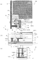
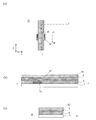
- FIGS. 4A to 4C are process plan views and cross-sectional views for explaining a method for manufacturing the active matrix substrate 1001.
- FIGS. 4A to 4C are process plan views and cross-sectional views for explaining a method for manufacturing the active matrix substrate 1001.
- FIGS. 4A to 4C are process plan views and cross-sectional views for explaining a method for manufacturing the active matrix substrate 1001.
- FIGS. 4A to 4C are process plan views and cross-sectional views for explaining a method for manufacturing the active matrix substrate 1001.
- FIGS. 4A to 4C are process plan views and cross-sectional views for explaining a method for manufacturing the active matrix substrate 1001.
- FIGS. 4A to 4C are process plan views and cross-sectional views for explaining a method for manufacturing the active matrix substrate 1001.
- FIGS. FIGS. 4A to 4C are process plan views and cross-sectional views for explaining a method for manufacturing the active matrix substrate 1001.
- FIGS. FIGS. 4A to 4C are process plan views and cross-sectional views for explaining a method for manufacturing the active matrix substrate 1001.
- FIGS. 4A to 4C are process plan views and cross-sectional views for explaining a method for manufacturing the active matrix substrate 1001.
- FIGS. FIGS. 4A to 4C are process plan views and cross-sectional views for explaining a method for manufacturing the active matrix substrate 1001.
- FIGS. 4A to 4C are process plan views and cross-sectional views for explaining a method for manufacturing the active matrix substrate 1001.
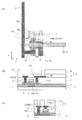
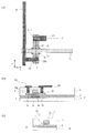
- FIGS. 7A to 7C are process plan views and cross-sectional views for explaining a method for manufacturing the active matrix substrate 1002;
- FIGS. 7A to 7C are process plan views and cross-sectional views for explaining a method for manufacturing the active matrix substrate 1002;
- FIGS. FIGS. 7A to 7C are process plan views and cross-sectional views for explaining a method for manufacturing the active matrix substrate 1002;
- FIGS. FIGS. 7A to 7C are process plan views and cross-sectional views for explaining a method for manufacturing the active matrix substrate 1002;
- FIGS. 7A to 7C are process plan views and cross-sectional views for explaining a method for manufacturing the active matrix substrate 1002;
- FIGS. FIGS. 7A to 7C are process plan views and cross-sectional views for explaining a method for manufacturing the active matrix substrate 1002;
- FIGS. FIGS. 7A to 7C are process plan views and cross-sectional views for explaining a method for manufacturing the active matrix substrate 1002;
- FIGS. FIGS. 7A to 7C are process plan views and cross-sectional views for explaining a method for manufacturing the active matrix substrate 1002;
- FIGS. FIGS. 7A to 7C are process plan views and cross-sectional views for explaining a method for manufacturing the active matrix substrate 1002;
- FIGS. FIGS. 7A to 7C are process plan views and cross-sectional views for explaining a method for manufacturing the active matrix substrate 1002;
- FIGS. FIGS. 7A to 7C are process plan views and cross-sectional views for explaining a method for manufacturing the active matrix substrate 1002;
- FIGS. 7A to 7C are process plan views and cross-sectional views for explaining a method for manufacturing the active matrix substrate 1002;
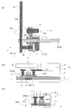
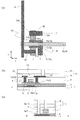
- FIGS. (A) is a plan view illustrating a pixel region PIX of the active matrix substrate 1003 of the second embodiment, and (b) and (c) are taken along lines II ′ and II-II ′, respectively. It is typical sectional drawing.
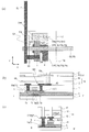
- FIGS. 7A to 7C are process plan views and cross-sectional views for explaining a method of manufacturing the active matrix substrate 1003.
- FIGS. FIGS. 7A to 7C are process plan views and cross-sectional views for explaining a method of manufacturing the active matrix substrate 1003.
- FIGS. 7A to 7C are process plan views and cross-sectional views for explaining a method of manufacturing the active matrix substrate 1003.
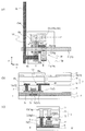
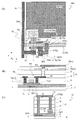
- FIGS. (A) is a plan view illustrating a pixel region PIX of the active matrix substrate 1004 of the second embodiment, and (b) and (c) are taken along lines II ′ and II-II ′, respectively. It is typical sectional drawing.
- (A) is a plan view illustrating a pixel region PIX of the active matrix substrate 1005 of the second embodiment, and (b) and (c) are taken along lines II ′ and II-II ′, respectively. It is typical sectional drawing.
- FIGS. 7A to 7C are process plan views and cross-sectional views for explaining a method of manufacturing the active matrix substrate 1005.
- FIGS. 7A to 7C are process plan views and cross-sectional views for explaining a method of manufacturing the active matrix substrate 1005.
- FIGS. FIGS. 7A to 7C are process plan views and cross-sectional views for explaining a method of manufacturing the active matrix substrate 1005.
- FIGS. (A) is a plan view illustrating a pixel region PIX of the active matrix substrate 1006 of the second embodiment, and (b) and (c) are taken along lines II ′ and II-II ′, respectively. It is typical sectional drawing.
- (A) is a plan view illustrating a pixel region PIX of the active matrix substrate 1007 of the second embodiment, and (b) and (c) are taken along lines II ′ and II-II ′, respectively. It is typical sectional drawing.
- FIGS. 7A to 7C are process plan views and cross-sectional views for explaining a method for manufacturing the active matrix substrate 1007.
- FIGS. 7A to 7C are process plan views and cross-sectional views for explaining a method for manufacturing the active matrix substrate 1007.
- (A) is a plan view illustrating a pixel region PIX of the active matrix substrate 1008 of the second embodiment, and (b) and (c) are taken along lines II ′ and II-II ′, respectively. It is typical sectional drawing.
- (A) is a plan view illustrating a pixel region PIX of the active matrix substrate 1009 of the second embodiment, and (b) and (c) are taken along lines II ′ and II-II ′, respectively. It is typical sectional drawing.
- FIGS. 9A to 9C are process plan views and cross-sectional views for explaining a method of manufacturing the active matrix substrate 1009.
- FIGS. FIGS. 9A to 9C are process plan views and cross-sectional views for explaining a method of manufacturing the active matrix substrate 1009.
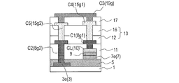
- FIGS. (A) is a plan view illustrating a pixel region PIX of the active matrix substrate 1010 of the second embodiment, and (b) and (c) are taken along lines II ′ and II-II ′, respectively. It is typical sectional drawing. It is sectional drawing which illustrates the other gate contact part in 2nd Embodiment. It is sectional drawing which illustrates the other gate contact part in 2nd Embodiment.
- FIGS. 7A to 7C are process plan views and cross-sectional views for explaining a method for manufacturing the active matrix substrate 1011.
- FIGS. 7A to 7C are process plan views and cross-sectional views for explaining a method for manufacturing the active matrix substrate 1011.
- FIGS. 7A to 7C are process plan views and cross-sectional views for explaining a method for manufacturing the active matrix substrate 1011.
- FIGS. 7A to 7C are process plan views and cross-sectional views for explaining a method for manufacturing the active matrix substrate 1011.
- FIGS. 7A to 7C are process plan views and cross-sectional views for explaining a method for manufacturing the active matrix substrate 1011.
- FIGS. 7A to 7C are process plan views and cross-sectional views for explaining a method for manufacturing the active matrix substrate 1011.
- FIGS. 7A to 7C are process plan views and cross-sectional views for explaining a method for manufacturing the active matrix substrate 1011.
- FIGS. 7A to 7C are process plan views and cross-sectional views for explaining a method for manufacturing the active matrix substrate 1011.
- FIGS. 7A to 7C are process plan views and cross-sectional views for explaining a method for manufacturing the active matrix substrate 1011.
- (A) is a plan view illustrating a pixel region PIX of the active matrix substrate 1012 of the second embodiment, and (b) and (c) are taken along lines II ′ and II-II ′, respectively. It is typical sectional drawing.
- FIG. (A) is a plan view illustrating an active matrix substrate 1013 pixel region PIX of the second embodiment, and (b) and (c) are schematic views taken along lines II ′ and II-II ′, respectively.
- FIG. (A) is a plan view illustrating a pixel region PIX of the active matrix substrate 1014 of the second embodiment, and (b) and (c) are taken along lines II ′ and II-II ′, respectively. It is typical sectional drawing.
- FIGS. 8A to 8C are process plan views and cross-sectional views for explaining a method of manufacturing the active matrix substrate 1014.
- FIGS. FIGS. 8A to 8C are process plan views and cross-sectional views for explaining a method of manufacturing the active matrix substrate 1014.
- FIGS. 8A to 8C are process plan views and cross-sectional views for explaining a method of manufacturing the active matrix substrate 1014.
- FIGS. FIGS. 8A to 8C are process plan views and cross-sectional views for explaining a method of manufacturing the active matrix substrate 1014.
- FIGS. (A) is a plan view illustrating a pixel region PIX of the active matrix substrate 1015 of the second embodiment, and (b) and (c) are taken along lines II ′ and II-II ′, respectively. It is typical sectional drawing.
- (A) is a plan view illustrating a pixel region PIX of the active matrix substrate 1016 of the second embodiment, and (b) and (c) are taken along lines II ′ and II-II ′, respectively. It is typical sectional drawing.
- FIGS. 1-10 are plan views illustrating a pixel region PIX of the active matrix substrate 1017 of the second embodiment, and (b) and (c) are taken along lines II ′ and II-II ′, respectively. It is typical sectional drawing.
- (A) is a plan view illustrating a pixel region PIX of another active matrix substrate of the first embodiment, and (b) and (c) are taken along lines II ′ and II-II ′, respectively. It is a typical sectional view. It is sectional drawing which illustrates the active-matrix board
- FIGS. 4A to 4C are process plan views and cross-sectional views for explaining a method for manufacturing an active matrix substrate of a reference example.
- FIGS. 4A to 4C are process plan views and cross-sectional views for explaining a method for manufacturing an active matrix substrate of a reference example.
- FIGS. 4A to 4C are process plan views and cross-sectional views for explaining a method for manufacturing an active matrix substrate of a reference example.
- FIGS. 4A to 4C are process plan views and cross-sectional views for explaining a method for manufacturing an active matrix substrate of a reference example.
- FIGS. 4A to 4C are process plan views and cross-sectional views for explaining a method for manufacturing an active matrix substrate of a reference example.
- FIGS. 4A to 4C are process plan views and cross-sectional views for explaining a method for manufacturing an active matrix substrate of a reference example.
- FIGS. 4A to 4C are process plan views and cross-sectional views for explaining a method for manufacturing an active matrix substrate of a
- FIGS. 4A to 4C are process plan views and cross-sectional views for explaining a method for manufacturing an active matrix substrate of a reference example.
- FIGS. 4A to 4C are process plan views and cross-sectional views for explaining a method for manufacturing an active matrix substrate of a reference example.
- an active matrix substrate in which the gate driver is monolithically formed and the source driver is mounted will be described as an example.
- an oxide semiconductor TFT top gate structure TFT or double gate structure TFT having an upper gate electrode may be formed as a pixel TFT.
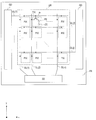
- FIG. 1 is a schematic diagram showing an example of a planar structure of the active matrix substrate of the present embodiment.
- the active matrix substrate has a display area DR and an area (non-display area or frame area) FR other than the display area DR.
- the display area DR is composed of pixel areas PIX arranged in a matrix.
- the pixel region PIX (sometimes simply referred to as “pixel”) is a region corresponding to a pixel of the display device.
- the non-display area FR is an area that is located around the display area DR and does not contribute to display.
- a plurality of gate bus lines GL (1) to GL (j) (j is an integer of 2 or more, hereinafter referred to as “gate bus line GL”) extending in the x direction (also referred to as row direction or second direction).
- a plurality of source bus lines SL (1) to SL (k) (k is an integer of 2 or more, hereinafter referred to as “source bus line SL”) extending in the y direction (also referred to as column direction or first direction).
- source bus line SL a plurality of source bus lines SL (1) to SL (k) (k is an integer of 2 or more, hereinafter referred to as “source bus line SL”) extending in the y direction (also referred to as column direction or first direction).
- Each pixel region PIX is defined by a gate bus line GL and a source bus line SL, for example.
- Each gate bus line GL is connected to each terminal of the gate driver GD.
- the source bus line SL is connected to each terminal of
- Each pixel region PIX includes a thin film transistor (pixel TFT) Pt and a pixel electrode PE.
- the thin film transistor Pt includes an upper gate electrode and a lower gate electrode (not shown). These gate electrodes are electrically connected to the corresponding gate bus lines GL.
- the source electrode of the thin film transistor Pt is electrically connected to the corresponding source bus line SL, and the drain electrode is electrically connected to the pixel electrode PE.
- a common electrode (common electrode) CE is provided for a plurality of pixels on the active matrix substrate.
- the common electrode CE is provided on a counter substrate that is disposed to face the active matrix substrate with a liquid crystal layer interposed therebetween.
- a gate driver GD for driving the gate bus line GL is integrally (monolithically) provided.
- peripheral circuits such as a source switching (SSD) circuit that drives the source bus lines SL in a time division manner may be integrally provided in the non-display area FR.
- SSD source switching
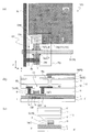
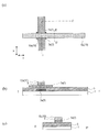
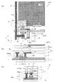
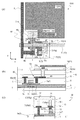
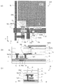
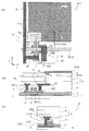
- FIG. 2A (a) is a plan view illustrating the pixel region PIX of the active matrix substrate 1001 of this embodiment.
- 2A (b) and 2 (c) are schematic cross-sectional views taken along lines I-I 'and II-II' shown in FIG. 2A (a), respectively.
- the active matrix substrate 1001 is applied to, for example, an FFS mode liquid crystal display device.
- components having substantially the same function are denoted by common reference numerals, and description thereof may be omitted.
- the pixel area PIX is an area surrounded by a source bus line SL extending in the y direction and a gate bus line GL extending in the x direction intersecting the source bus line SL.
- the pixel region PIX includes a substrate 1, a TFT (pixel TFT) 101 supported on the substrate 1, a lower transparent electrode 15, and an upper transparent electrode 19.
- the upper transparent electrode 19 has a slit or notch for each pixel.
- the lower transparent electrode 15 is a common electrode CE
- the upper transparent electrode 19 is a pixel electrode PE.
- the TFT 101 is, for example, an oxide semiconductor TFT having a double gate structure.
- the TFT 101 includes an oxide semiconductor layer 7 having an active region 7a, a lower gate electrode 3a disposed on the substrate 1 side of the oxide semiconductor layer 7 via a lower insulating layer 5, and an upper side of the oxide semiconductor layer 7 (substrate 1), an upper gate electrode 10a disposed via an upper insulating layer 9, and a source electrode 8S and a drain electrode 8D.
- Lower gate electrode 3a and upper gate electrode 10a are electrically connected to corresponding gate bus line GL
- source electrode 8S is electrically connected to corresponding source bus line SL.
- the drain electrode 8D is electrically connected to the pixel electrode PE.
- the lower gate electrode 3a is disposed so as to overlap with a part of the active region 7a when viewed from the normal direction of the substrate 1. Note that the lower gate electrode 3a only needs to overlap with at least a part of the active region 7a, and may overlap with the entire active region 7a.
- the upper gate electrode 10 a is disposed so as to overlap with a part of the active region 7 a when viewed from the normal direction of the substrate 1.
- each pixel area PIX will be described in more detail.
- the pixel region PIX includes a lower gate layer 3 supported by the substrate 1, a lower insulating layer 5 covering the lower gate layer 3, an oxide semiconductor layer 7 disposed on the lower insulating layer 5, and an oxide semiconductor layer. 7 is provided with an upper gate layer 10 disposed via an upper insulating layer 9.
- the oxide semiconductor layer 7 includes an active region 7 a of the TFT 101.
- the lower gate layer 3 includes a lower gate electrode 3 a of the TFT 101.
- the upper gate layer 10 includes an upper gate electrode 10 a of the TFT 101.
- the upper insulating layer 9 is disposed on a part of the oxide semiconductor layer 7 so as not to contact the lower insulating layer 5.
- the upper insulating layer 9 may be disposed only between the oxide semiconductor layer 7 and the upper gate layer 10.
- One of the lower gate electrode 3a and the upper gate electrode 10a may be formed integrally with one corresponding gate bus line GL using the same conductive film as the gate bus line GL (for example, It may be part of the gate bus line GL). That is, one of the lower gate layer 3 and the upper gate layer 10 may include the gate bus line GL formed integrally with the lower gate electrode 3a or the upper gate electrode 10a.
- the upper gate layer 10 includes an upper gate electrode 10a and a gate bus line GL formed integrally with the upper gate electrode 10a.
- the lower gate layer 3 is formed in an island shape in the pixel region PIX.
- the oxide semiconductor layer 7 When viewed from the normal direction of the substrate 1, the oxide semiconductor layer 7 has an active region 7a located in a region where the TFT 101 is formed (TFT formation region) and an extending region 7e extending from the active region 7a. ing.
- the extended region 7 e is disposed on the substrate 1 side of the upper gate layer 10 via the upper insulating layer 9.
- the extension region 7e may extend in a direction different from the channel length direction of the TFT 101 from the active region 7a.
- the active region 7a and the extended region 7e are integrally formed.
- the extended region 7e is disposed on the substrate 1 side of the gate bus line GL of the upper gate layer 10 via the upper insulating layer 9, and when viewed from the normal direction of the substrate 1, the active region 7a To the gate bus line GL (here, extending in the x direction).
- the step of the gate bus line GL can be reduced.
- the on-current can flow (around) the extended region 7e, and the effective channel width may be increased.
- the extension region 7e of the oxide semiconductor layer 7 connects the active regions 7a in the two pixel regions PIX adjacent in the x direction so as to overlap the gate bus line GL when viewed from the normal direction of the substrate 1. It may extend.
- the oxide semiconductor layer 7 may have a pattern in which the active regions 7a in the plurality of pixel regions PIX arranged in the x direction are connected via the extended region 7e.
- the peripheral edge of the extended region 7e may be aligned with the peripheral edge of the gate bus line GL, or may be located inside the peripheral edge of the gate bus line GL.
- the oxide semiconductor layer 7 can be formed, for example, by patterning the oxide semiconductor film after patterning the upper gate electrode 10a and the upper insulating layer 9. Thereby, when the upper insulating layer 9 is patterned, the oxide semiconductor film can function as an etch stop, so that over-etching of the lower insulating layer 5 is suppressed. In this case, substantially the entire lower surface of the upper insulating layer 9 may be in contact with the oxide semiconductor layer 7. Note that depending on the patterning conditions of the oxide semiconductor layer 7, a part of the lower surface (peripheral portion) of the upper insulating layer 9 may not contact the oxide semiconductor layer 7.
- the source electrode 8S and the drain electrode 8D are electrically connected to the active region 7a of the oxide semiconductor layer 7.
- the source electrode 8S and the drain electrode 8D may be formed using the same conductive film as the source bus line SL (FIG. 1).
- a layer formed using the same conductive film as the source bus line SL is referred to as a “source metal layer”.
- a layer formed using the same conductive film as the gate bus line GL is referred to as a “gate metal layer”.
- the oxide semiconductor layer 7, the upper insulating layer 9, and the upper gate electrode 10a may be covered with an inorganic insulating layer (passivation film) 11.
- the source electrode 8S is in contact with a part of the active region 7a on the first inorganic insulating layer 11 and in the source opening CHs formed in the first inorganic insulating layer 11.
- the drain electrode 8D is in contact with the other part of the active region 7a on the first inorganic insulating layer 11 and in the drain opening CHd formed in the first inorganic insulating layer 11.
- a portion in contact with the source electrode 8S is referred to as a source contact region 7s
- a portion in contact with the drain electrode 8D is referred to as a drain contact region 7d.
- channel region 7c a region located between the source contact region 7s and the drain contact region 7d and overlapping with at least one of the lower gate electrode 3a and the upper gate electrode 10a.
- the active region 7a may further include an offset region 7off located between the channel region 7c and the source contact region 7s and / or the drain contact region 7d.
- the upper insulating layer 9 may be formed only between the oxide semiconductor layer 7 and the upper gate layer 10. Accordingly, the channel region 7c of the oxide semiconductor layer 7 and the regions other than the channel region (the offset region 7off, the contact regions 7s and 7d) in the active region 7a can be brought into contact with different insulating films.
- the upper insulating layer 9 is formed using an oxide film such as a silicon oxide film, oxidation defects generated in the channel region 7c of the oxide semiconductor layer 7 can be reduced by the oxide film, so that desired TFT characteristics can be obtained. It can be secured.
- the first inorganic insulating layer 11 is formed using an insulating film that reduces an oxide semiconductor such as a silicon nitride film, a region of the oxide semiconductor layer 7 that is in contact with the first inorganic insulating layer 11 is reduced in resistance. Therefore, a decrease in on-resistance can be suppressed. In particular, when the offset region 7off is in contact with the first inorganic insulating layer 11, it is possible to more effectively suppress a decrease in on-resistance.
- the upper gate layer 10 and the upper insulating layer 9 may be patterned using the same mask, for example.
- the periphery of the gate bus line GL or the upper gate electrode 10 a that is, the periphery of the upper gate layer 10
- the periphery of the upper insulating layer 9 may be aligned. Further, substantially the entire lower surface of the upper gate layer 10 may be in contact with the upper insulating layer 9.
- an interlayer insulating layer 13 is provided so as to cover the TFT 101.
- the interlayer insulating layer 13 includes, for example, a second inorganic insulating layer 12 and an organic insulating layer 16 disposed on the second inorganic insulating layer 12.
- the interlayer insulating layer 13 may not include the organic insulating layer 16.
- a lower transparent electrode 15 is disposed on the interlayer insulating layer 13.
- An upper transparent electrode 19 is disposed on the lower transparent electrode 15 via a dielectric layer 17.
- One of the lower transparent electrode 15 and the upper transparent electrode 19 (here, the upper transparent electrode 19) functions as the pixel electrode PE, and the other (here, the lower transparent electrode 15) functions as the common electrode CE.
- the pixel electrode PE is separated for each pixel.
- the common electrode CE may not be separated for each pixel.
- the common electrode CE may have an opening 15p on a region where the TFT 101 and the gate contact portion 30 are formed, and may be formed over the entire pixel region PIX except this region.
- the pixel electrode PE is electrically connected to the drain electrode 8D of the TFT 101 at the pixel contact portion.
- the pixel electrode PE is electrically connected to the drain electrode 8D through an island-shaped transparent connection portion 15a formed using the same transparent conductive film as the common electrode CE.
- the pixel electrode PE is in contact with the transparent connection portion 15 a in the opening portion 17 m formed in the dielectric layer 17.
- the transparent connection portion 15a is in contact with the drain electrode 8D in the opening 13m formed in the interlayer insulating layer 13.
- a contact hole hereinafter referred to as a “pixel contact hole” CHp constituted by the opening 17m and the opening 13m does not overlap with the drain opening CHd.
- the contact hole CHp may partially or entirely overlap with the drain opening CHd.
- the TFT 101 is arranged so that the channel length direction DL of the TFT 101 is in the y direction (the direction in which the source bus line SL extends) (TFT vertical structure).
- the channel length direction DL indicates a direction in which a current flows in the channel region 7c in a plane parallel to the substrate 1
- the channel width direction DW indicates a direction orthogonal to the channel length direction DL.
- the active region 7 a of the semiconductor layer 7 may extend in the y direction so as to intersect the gate bus line GL when viewed from the normal direction of the substrate 1.
- the TFT 101 may be arranged so that the channel length direction DL is in the x direction (TFT horizontal structure).
- a gate contact portion for electrically connecting the lower gate electrode 3a of the TFT 101 and the upper gate electrode 10a (or the gate bus line GL) may be provided in the pixel region PIX.
- the lower gate electrode 3a does not have to be island-shaped.
- the lower gate electrode 3a may be a part of another gate wiring extending in the x direction.
- the other gate wiring may be electrically connected to the gate bus line GL in the non-display area.
- the pixel TFT in this embodiment may be a top gate structure TFT.
- the top gate structure TFT may have the same configuration as the TFT 101 except that the top gate structure TFT does not have the lower gate electrode 3a.
- the lower gate electrode 3a may function as a light-shielding film without functioning as a gate electrode.
- the active matrix substrate 1001 may have a monolithic peripheral circuit (such as a gate driver).
- the peripheral circuit includes a circuit TFT.
- the circuit TFT may be an oxide semiconductor TFT having a double gate structure similar to the TFT 101, for example.
- the circuit TFT may be a crystalline silicon TFT.
- the active matrix substrate 1001 can be applied to, for example, an FFS mode or IPS mode display device.
- the FFS mode is a transverse electric field mode in which a pair of electrodes is provided on one substrate and an electric field is applied to liquid crystal molecules in a direction parallel to the substrate surface (lateral direction).
- an electric field expressed by electric lines of force that exit from the pixel electrode PE pass through a liquid crystal layer (not shown), and further pass through the slit-like opening of the pixel electrode PE to the common electrode CE is generated.
- This electric field has a component transverse to the liquid crystal layer.
- a horizontal electric field can be applied to the liquid crystal layer.
- the horizontal electric field method has an advantage that a wider viewing angle can be realized than the vertical electric field method because liquid crystal molecules do not rise from the substrate.
- An electrode structure in which the pixel electrode PE is disposed on the common electrode CE via the dielectric layer 17 is described in, for example, International Publication No. 2012/0886513.
- the common electrode CE may be disposed on the pixel electrode PE via the dielectric layer 17. That is, the lower transparent electrode 15 formed on the lower transparent conductive layer may be the pixel electrode PE, and the upper transparent electrode 19 formed on the upper transparent conductive layer may be the common electrode CE.
- Such electrode structures are described in, for example, Japanese Patent Application Laid-Open Nos. 2008-032899 and 2010-008758.
- the entire disclosures of International Publication No. 2012/086513, Japanese Patent Application Laid-Open No. 2008-032899, and Japanese Patent Application Laid-Open No. 2010-008758 are incorporated herein by reference.
- the active matrix substrate of the present embodiment may not have the common electrode CE.
- Such an active matrix substrate can be used for a display device such as a TN (Twisted Nematic) mode or a VA (Vertical Alignment).
- the VA mode and the TN mode are longitudinal electric field mode modes in which an electric field is applied to liquid crystal molecules by a pair of electrodes arranged with a liquid crystal layer interposed therebetween.
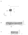
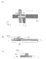
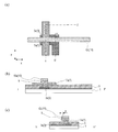
- FIGS. 2B to 2I are schematic process diagrams for explaining a method of manufacturing the active matrix substrate 1001.
- FIG. (A) of each figure is a top view which illustrates pixel area PIX.
- FIGS. 2B and 2C are schematic cross-sectional views taken along lines I-I ′ and II-II ′ shown in FIG. 2A, respectively.
- an island-shaped lower gate layer 3 is formed on the substrate 1 in each pixel region PIX.
- a lower gate conductive film thickness: for example, 50 nm or more and 500 nm or less
- an insulating substrate for example, a glass substrate
- the lower gate conductive layer is patterned to obtain the lower gate layer 3 including the lower gate electrode 3a.
- the substrate for example, a glass substrate, a silicon substrate, a heat-resistant plastic substrate (resin substrate), or the like can be used.
- the lower gate conductive film for example, a metal containing an element selected from aluminum (Al), chromium (Cr), copper (Cu), tantalum (Ta), titanium (Ti), molybdenum (Mo) or tungsten (W)
- a film or an alloy film containing these elements as a component can be used.
- a laminated film having a three-layer structure of titanium film-aluminum film-titanium film or a three-layer structure of molybdenum film-aluminum film-molybdenum film can be used.
- the gate conductive film is not limited to a three-layer structure, and may have a single layer, a two-layer structure, or a stacked structure of four or more layers.
- a laminated film having a Ti film (thickness: 15 to 70 nm) as a lower layer and a Cu film (thickness: 200 to 400 nm) as an upper layer is used as the lower gate conductive film.
- a lower insulating layer (thickness: for example, 200 nm or more and 500 nm or less) 5 that covers the lower gate layer 3 is formed.
- the lower insulating layer 5 includes a silicon oxide (SiO 2 ) layer, a silicon nitride (SiNx) layer, a silicon oxynitride (SiOxNy; x> y) layer, a silicon nitride oxide (SiNxOy; x> y) layer, an aluminum oxide layer, or A tantalum oxide layer or the like can be used as appropriate.
- the lower insulating layer 5 may have a laminated structure.
- a CVD method is used to form a laminated film having a silicon nitride (SiNx) layer (thickness: 100 to 500 nm) as a lower layer and a silicon oxide (SiO 2 ) layer (thickness: 20 to 100 nm) as an upper layer.
- SiNx silicon nitride
- SiO 2 silicon oxide
- an oxide semiconductor film (thickness: 15 nm to 200 nm or less) 7 ′ and an upper insulating film (thickness: 80 nm to 250 nm, for example) are formed on the lower insulating layer 5.
- 9 ′ and an upper gate conductive film (thickness: for example, 50 nm or more and 500 nm or less) 10 ′ are formed in this order.
- the oxide semiconductor film 7 ′ and the upper gate conductive film 10 ′ can be formed by, for example, sputtering, and the upper insulating film 9 ′ can be formed by CVD.
- the oxide semiconductor film 7 ′ is not particularly limited, but may be, for example, an In—Ga—Zn—O-based semiconductor film.
- As the upper insulating film 9 ′ an insulating film similar to the lower insulating layer 5 (an insulating film exemplified as the lower insulating layer 5) can be used.
- As the upper gate conductive film 10 ' a conductive film similar to the lower gate conductive film can be used.
- a silicon oxide (SiO 2 ) film is used as the upper insulating film 9 ′.
- As the upper gate conductive film 10 ′ a laminated film having a Ti film (thickness: 15 to 70 nm) as a lower layer and a Cu film (thickness: 200 to 400 nm) as an upper layer is used.
- the upper insulating film 9' and the upper gate conductive film 10 ' are formed on the oxide semiconductor film 7' without patterning. Thereby, it is possible to suppress the lower insulating layer 5 from being over-etched in the patterning step of the upper insulating film 9 ′ described later.
- the upper gate conductive film 10 ′ is patterned using a first resist mask (not shown) to include the upper gate electrode 10a and the gate bus line GL.
- An upper gate layer 10 is formed.
- the patterning of the upper gate conductive film 10 ′ can be performed by wet etching or dry etching.
- the upper insulating film 9 ' is patterned using the first resist mask.
- the patterning of the upper insulating film 9 ' can be performed by dry etching, for example.
- the oxide semiconductor film 7 ′ functions as an etch stop, and the etching of the surface of the lower insulating layer 5 can be suppressed.
- the first resist mask is removed.
- the upper insulating layer 9 and the upper gate electrode 10a are formed using the same mask, the side surface of the upper insulating layer 9 and the side surface of the upper gate electrode 10a or the gate bus line GL are aligned in the thickness direction. . That is, the periphery of the upper insulating layer 9 is aligned with the periphery of the upper gate layer 10 when viewed from the normal direction of the substrate 1.
- the oxide semiconductor film 7 ′ is patterned using a second resist mask (not shown) that defines the active region, and the oxide semiconductor layer 7 Get.
- the patterning of the oxide semiconductor film 7 ′ is performed by wet etching using, for example, the second resist mask and the upper gate layer 10 as an etching mask. Thereafter, the second resist mask is removed. Thereby, the oxide semiconductor layer 7 including the active region 7a and the extending region 7e extending in the x direction below the gate bus line GL is obtained.
- the oxide semiconductor layer 7 has one connected pattern for each pixel row (for each row in which the plurality of pixel regions PIX are arranged in the x direction). That is, the oxide semiconductor layers 7 in the pixel region PIX adjacent in the x direction are integrally formed (connected), but the oxide semiconductor layers 7 in the pixel region PIX adjacent in the y direction are separated from each other. Yes (not connected).
- a stacked body composed of the upper gate layer 10, the upper insulating layer 9, and the oxide semiconductor layer 7 is formed.
- the substantially entire lower surfaces of the upper gate electrode 10 a and the gate bus line GL may be in contact with the upper insulating layer 9, and the substantially entire lower surface of the upper insulating layer 9 may be in contact with the oxide semiconductor layer 7.
- the first inorganic insulating layer (thickness: 100 nm or more and 500 nm or less) is formed so as to cover the oxide semiconductor layer 7, the upper insulating layer 9, and the upper gate layer 10. 11 is formed. Thereafter, openings CHs and CHd reaching the oxide semiconductor layer 7 are formed in the first inorganic insulating layer 11 by dry etching, for example.
- a silicon oxide film, a silicon nitride film, a silicon oxynitride film, or a silicon nitride oxide film can be formed as a single layer or a stacked layer.
- a SiNx layer thickness: 300 nm is formed by a CVD method.
- a source metal layer including a source bus line SL, a source electrode 8S, and a drain electrode 8D is formed.
- a source conductive film (thickness: for example, 50 nm to 500 nm) is formed on the first inorganic insulating layer 11 and in the openings CHs and CHd, and the source conductive film is patterned. Patterning can be performed by dry etching or wet etching.
- the source electrode 8S is in contact with the active region 7a of the oxide semiconductor layer 7 in the source opening CHs, and the drain electrode 8D is in contact with the active region 7a in the drain opening CHd. In this way, the TFT 101 is obtained.
- the conductive film for the source for example, an element selected from aluminum (Al), chromium (Cr), copper (Cu), tantalum (Ta), titanium (Ti), molybdenum (Mo) or tungsten (W), or these An alloy containing any of these elements as a component can be used.
- a three-layer structure of titanium film-aluminum film-titanium film, a three-layer structure of molybdenum film-aluminum film-molybdenum film, or the like may be used.
- the source conductive film is not limited to a three-layer structure, and may have a single layer, a two-layer structure, or a stacked structure of four or more layers.
- a laminated film having a Ti film (thickness: 15 to 70 nm) as a lower layer and a Cu film (thickness: 200 to 400 nm) as an upper layer is used.
- the material of the second inorganic insulating layer 12 may be the same as the material exemplified as the material of the first inorganic insulating layer 11.
- a SiNx layer is formed as the second inorganic insulating layer 12 by a CVD method.
- the organic insulating layer 16 may be, for example, an organic insulating film containing a photosensitive resin material.
- the organic insulating layer 16 is patterned to form openings.
- the second inorganic insulating layer 12 is etched (dry etching) using the organic insulating layer 16 as a mask. Thereby, an opening 13m reaching the drain electrode 8D is formed in the second inorganic insulating layer 12 and the organic insulating layer 16.
- a lower transparent conductive layer including the lower transparent electrode 15 and the transparent connection portion 15a is formed.
- a first transparent conductive film (thickness: 20 to 300 nm) is formed on the interlayer insulating layer 13 and in the opening 13m.
- an indium-zinc oxide film is formed as the first transparent conductive film by a sputtering method.
- a metal oxide such as indium-tin oxide (ITO), indium-zinc oxide, or ZnO can be used.
- the first transparent conductive film is patterned by wet etching, for example. Thereby, the lower transparent electrode 15 and the transparent connection part 15a are obtained.
- the transparent connection portion 15a is disposed so as to be in contact with the drain electrode 8D within the opening 13m.
- the lower transparent electrode 15 is formed over the plurality of pixel regions PIX and functions as the common electrode CE.
- the lower transparent electrode 15 has an opening 15p on the TFT formation region and the pixel contact portion.
- the transparent connection portion 15 a is disposed inside the opening portion 15 p with a space from the lower transparent electrode 15.
- a dielectric layer (thickness: 50 to 500 nm) 17 is formed on the interlayer insulating layer 13 and the lower transparent electrode 15. Thereafter, an opening 17m is formed in the dielectric layer 17 to expose a part of the transparent connection portion 15a.
- the opening 17m may be disposed so that at least a part thereof overlaps the opening 13m of the interlayer insulating layer 13.
- the material of the dielectric layer 17 may be the same as the material exemplified as the material of the first inorganic insulating layer 11.
- a SiN film is formed by, for example, the CVD method.
- a second transparent conductive film (thickness: 20 to 300 nm) is formed on the dielectric layer 17 and in the opening 17m. Thereafter, the second transparent conductive film is patterned to form an upper transparent conductive layer including the upper transparent electrode 19 functioning as the pixel electrode PE on the dielectric layer 17.
- the upper transparent electrode 19 is provided with at least one opening (or notch) for each pixel.
- the material of the second transparent conductive film may be the same as the material exemplified as the material of the first transparent conductive film.
- the second transparent conductive film may be a single layer or a laminated film.
- an indium-zinc oxide film is formed by a sputtering method.
- a part of the upper transparent electrode 19 may be arranged so as to overlap the lower transparent electrode 15 with the dielectric layer 17 interposed therebetween to constitute an auxiliary capacitor. In this way, the active matrix substrate 1001 shown in FIG. 2A is manufactured.
- the present inventor forms an upper insulating layer after patterning an oxide semiconductor layer. Found a problem.
- FIGS. 21A to 21G are schematic process diagrams for explaining a method of manufacturing an active matrix substrate of a reference example.
- A) of each figure is a top view which illustrates pixel area PIX.
- B) and (c) of each figure are schematic cross-sectional views taken along lines I-I ′ and II-II ′, respectively.
- the same components as those in FIGS. 2A to 2I are denoted by the same reference numerals.
- an island-shaped lower gate electrode 3a and a lower insulating layer 5 covering the lower gate electrode 3a are formed on the substrate 1 in each pixel region PIX.
- an upper insulating film 9 'and an upper gate conductive film 10' are formed so as to cover the oxide semiconductor layer 97.
- the upper gate conductive film 10 ′ is patterned using a first resist mask (not shown) to include the upper gate electrode 10a and the gate bus line GL.
- the upper gate layer 10 is obtained.
- the upper insulating film 9 ' is patterned by dry etching using the first resist mask as it is. At this time, the surface portion of the region 5n not covered with the oxide semiconductor layer 97 in the lower insulating layer 5 may be etched (overetched).
- a first inorganic insulating layer 11 is deposited so as to cover the oxide semiconductor layer 97, the upper insulating layer 9, and the upper gate layer 10, and the first inorganic insulating layer is deposited.
- a source opening CHs and a drain opening CHd are formed in the layer 11. At this time, the coverage of the first inorganic insulating layer 11 may be lowered on the over-etched region 5 n of the lower insulating layer 5.
- a source conductive film is formed on the first inorganic insulating layer 11 and in the source opening CHs and the drain opening CHd, and patterned to form a source.
- a source metal layer including the electrode 8S and the drain electrode 8D is formed.
- the interlayer insulating layer 13, the lower transparent electrode 15, the transparent connection portion 15a, the dielectric layer 17, and the upper transparent electrode 19 are formed in the same manner as in the steps described in FIGS. 2H and 2I. In this way, the TFT of the reference example is manufactured.
- the oxide semiconductor layer 97 is formed in an island shape in each pixel region PIX.
- the oxide semiconductor layer 97 is disposed only in the TFT formation region, for example.
- the upper insulating layer 9 is positioned below the gate bus line GL, but the oxide semiconductor layer 97 is not positioned.
- the coverage of the first inorganic insulating layer 11 is lowered due to over-etching of the lower insulating layer 5, and the reliability of the TFT may be lowered.
- the manufacturing method (FIGS. 2B to 2I) of the TFT 101 of the present embodiment before the oxide semiconductor film 7 ′ is patterned, that is, the lower insulating layer 5 is protected by the oxide semiconductor film 7 ′. In this state, the upper insulating layer 9 is patterned. For this reason, in the patterning process of the upper insulating layer 9, the oxide semiconductor film 7 'functions as an etch stop, and over-etching of the lower insulating layer 5 can be suppressed. Accordingly, it is possible to suppress a decrease in reliability due to over-etching of the lower insulating layer 5.
- the portion of the oxide semiconductor film 7 ′ that becomes the extended region 7e of the oxide semiconductor layer 7 is formed in a state protected by the upper insulating layer 9, and thus the extended region 7e Lowering resistance due to process damage or the like can be suppressed. For this reason, even if the active regions 7a of the adjacent pixel regions are connected by the extended region 7e, the display operation is not affected.
- a gate contact portion for electrically connecting an upper gate electrode and a lower gate electrode is provided in each pixel region PIX.
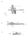
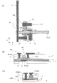
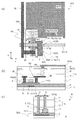
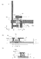
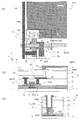
- FIG. 3A (a) is a plan view illustrating the pixel region PIX of the active matrix substrate 1002 of this embodiment.
- 3A (b) and 3 (c) are schematic cross-sectional views taken along lines I-I 'and II-II' shown in FIG. 3A (a), respectively.
- Each pixel region PIX of the active matrix substrate 1002 has a gate contact portion 30 that electrically connects the lower gate layer 3 and the upper gate layer 10.
- the gate contact portion 30 may be disposed in the vicinity of the TFT 101 and separated from the active region 7 a.
- the lower gate layer 3 and the upper gate layer 10 are electrically connected via a connection portion (referred to as a “gate connection portion C”) formed in a layer different from the lower gate electrode 3a and the upper gate electrode 10a. It is connected to the.
- the gate contact portion 30 may include a first portion 31 that connects the gate connection portion C and the upper gate layer 10, and a second portion 32 that connects the gate connection portion C and the lower gate layer 3.
- the gate connection portion C is formed using, for example, a conductive film that is above the upper gate layer 10.
- the gate connection portion C is an island-shaped connection portion 8g formed using the same conductive film as the source bus line SL.
- the lower gate layer 3 includes a lower gate electrode 3a that functions as a gate located in the TFT formation region, and a lower gate extension portion 3e that extends from the lower gate electrode 3a (from the TFT formation region) to the second portion 32. It has an island-like pattern including The lower gate electrode 3a is disposed so as to overlap with at least a part of the active region 7a when viewed from the normal direction of the substrate 1.
- the lower gate extension 3e is formed integrally with the lower gate electrode 3a. As illustrated, the lower gate extension 3e extends in the x direction from the TFT formation region to the first portion 31 so as to overlap the gate bus line GL, and overlaps the connection portion 8g from the first portion 31 to the second portion 32. It may extend like this. Thereby, it is possible to suppress a decrease in the pixel aperture ratio due to the lower gate extension 3e.
- the connecting portion 8g extends so as to connect the first portion 31 and the second portion 32.
- the connecting portion 8g extends in the y direction, but the extending direction is not particularly limited.
- the connecting portion 8g is in contact with the gate bus line GL in the opening portion 11p formed in the first inorganic insulating layer 11 in the first portion 31.
- the upper insulating layer 9 and the extended region 7e of the oxide semiconductor layer 7 are arranged on the substrate 1 side of the gate bus line GL.
- the connection portion 8g is in contact with the lower gate extension portion 3e in the opening 11q formed in the lower insulating layer 5 and the first inorganic insulating layer 11 in the second portion 32.
- the extended region 7 e of the upper insulating layer 9 and the oxide semiconductor layer 7 is located between the upper gate layer 10 and the lower insulating layer 5.
- the oxide semiconductor layer 7 may be patterned after the upper gate layer 10 and the upper insulating layer 9 are patterned using the same mask. Thereby, when viewed from the normal direction of the substrate 1, the peripheral edge of the upper gate layer 10 including the gate bus line GL and the upper gate electrode 10a, the peripheral edge of the upper insulating layer 9, and the extended region 7e of the oxide semiconductor layer 7 are provided. It is substantially aligned with the peripheral edge.
- the first portion 31 may be disposed on the gate bus line GL, and the second portion 32 may be disposed at a position separated from the gate bus line GL in the y direction.
- the first portion 31 and the second portion 32 are sufficiently spaced so that the extended region 7e of the oxide semiconductor layer 7 located in the first portion 31 does not contact the connecting portion 8g in the opening 11q. It is arranged with a gap.
- the gate contact portion 30 When viewed from the normal direction of the substrate 1, the gate contact portion 30 extends substantially parallel to the active region 7 a (here, in the y direction), but the shape and arrangement of the gate contact portion 30 are illustrated in the illustrated example. It is not limited.
- the gate connection portion C may extend from the first portion 31 to the second portion 32 so as to overlap the lower gate extension portion 3e.
- the first portion 31 may be arranged so as not to overlap the lower gate extension 3e when viewed from the normal direction of the substrate 1 (see FIG. 5 and the like).
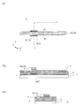
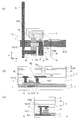
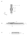
- FIGS. 3B to 3J are schematic process diagrams for explaining a method of manufacturing the active matrix substrate 1002.
- FIG. (A) of each figure is a top view which illustrates pixel area PIX.
- FIGS. 3B and 3C are schematic cross-sectional views taken along lines I-I ′ and II-II ′ shown in FIG. 3A, respectively.
- an island-shaped lower gate layer 3 and a lower insulating layer 5 are formed on the substrate 1 in each pixel region PIX.
- the lower gate layer 3 includes a lower gate electrode 3a and a lower gate extension portion 3e extending from the TFT formation region to a region for forming a gate contact portion.
- an oxide semiconductor film 7 ', an upper insulating film 9', and an upper gate conductive film 10 ' are formed in this order on the lower insulating layer 5.
- the upper gate conductive film 10 ′ is patterned using a first resist mask (not shown) to include the upper gate electrode 10a and the gate bus line GL.
- An upper gate layer 10 is formed.
- the upper insulating film 9 ' is patterned using the first resist mask. Similar to the above-described embodiment, in this patterning step, since the lower insulating layer 5 is covered with the oxide semiconductor film 7 ′, the oxide semiconductor film 7 ′ functions as an etch stop. It can suppress that the surface is etched. Thereafter, the first resist mask is removed. Note that, after removing the first resist mask, the upper insulating film 9 ′ may be patterned using the upper gate layer 10 as a mask.
- the oxide semiconductor film 7 ′ is patterned using a second resist mask (not shown) defining the active region and the upper gate layer 10 as a mask.
- the oxide semiconductor layer 7 is obtained.
- the oxide semiconductor layer 7 includes an active region 7a defined by the second resist mask and an extended region 7e extending from the active region 7a so as to overlap the upper gate layer 10.
- the extension region 7e includes a portion extending in the x direction below the gate bus line GL.
- a first inorganic insulating layer 11 is formed so as to cover the oxide semiconductor layer 7, the upper insulating layer 9, and the upper gate layer 10. Thereafter, for example, by dry etching, openings CHs and CHd reaching the oxide semiconductor layer 7 in the first inorganic insulating layer 11, openings 11p reaching the gate bus lines GL, and openings reaching the lower gate extension 3e. 11q.
- a source metal layer including a source bus line SL, a source electrode 8S and a drain electrode 8D, and a gate connection portion C (connection portion 8g) is formed.
- the connecting portion 8g is disposed so as to be in contact with the gate bus line GL in the opening portion 11p and in contact with the lower gate extension portion 3e in the opening portion 11q. In this way, the gate contact portion 30 and the TFT 101 are obtained.
- the lower transparent conductive layer including the interlayer insulating layer 13, the lower transparent electrode 15 and the transparent connection portion 15a, and the dielectric The body layer 17 is formed.
- the formation method is the same as that described above with reference to FIGS. 2H and 2I.
- an upper transparent conductive layer including the upper transparent electrode 19 is formed. In this way, the active matrix substrate 1002 shown in FIG. 3A is manufactured.
- a gate contact portion 30 that electrically connects the lower gate layer 3 and the upper gate layer 10 is provided for each pixel region PIX. Accordingly, one of the lower gate layer 3 and the upper gate layer 10 can be formed in an island shape within the pixel region PIX, and thus a decrease in pixel aperture ratio can be suppressed. Further, similarly to the above-described embodiment, by performing the patterning of the oxide semiconductor layer 7 after the formation of the gate metal layer, it is possible to suppress a decrease in reliability due to overetching of the lower insulating layer 5.
- the extended region 7e of the oxide semiconductor layer 7 and the connection portion 8g can be more electrically separated from each other, so that the TFT 101 can be formed. It can be operated more stably.
- the gate connection portion C that connects the lower gate layer 3 and the upper gate layer 10 is formed using the same transparent conductive film (first transparent conductive film) as the lower transparent electrode 15. It differs from the active matrix substrate 1002 shown in FIG. 3A in that it is formed.
- FIG. 4A (a) is a plan view illustrating the pixel region PIX of the active matrix substrate 1003 of Modification Example 1 of this embodiment.
- 4A (b) and 4 (c) are schematic cross-sectional views taken along lines I-I 'and II-II' shown in FIG. 4A (a), respectively.
- the gate contact portion 30 has a connection portion 15g formed using the same transparent conductive film as the lower transparent electrode 15 as the gate connection portion C.
- the connecting portion 15g is in contact with the upper gate layer 10 (here, the gate bus line GL) in the contact hole CH1 formed in the first inorganic insulating layer 11 and the interlayer insulating layer 13 in the first portion 31.
- the connecting portion 15g is connected to the lower gate layer 3 (lower gate extending portion 3e) in the contact hole CH2 formed in the lower insulating layer 5, the first inorganic insulating layer 11, and the interlayer insulating layer 13. Is in contact with.
- Other configurations may be the same as those of the active matrix substrate 1002.
- the active matrix substrate 1003 of Modification 1 can be manufactured as follows.
- the lower gate electrode 3a, the lower insulating layer 5, the oxide semiconductor layer 7, the upper insulating layer 9, the upper gate electrode 10a, the gate bus line GL and the first gate electrode GL are formed on the substrate 1.
- the inorganic insulating layer 11 is formed.
- openings CHs, CHd, 11p, and 11q are formed in the first inorganic insulating layer 11.
- a source conductive film is formed and patterned to form the source electrode 8S and the drain electrode 8D.
- the source conductive film is removed from the gate contact portion formation region.
- the second inorganic insulating layer 12 and the organic insulating layer 16 are formed so as to cover the TFT 101. Thereafter, the organic insulating layer 16 is patterned to form an opening. Subsequently, the second inorganic insulating layer 12 is etched (dry etching) using the organic insulating layer 16 as a mask. Thereby, the opening 13m reaching the drain electrode 8D and the openings 13p and 13q located in the gate contact portion formation region are formed in the second inorganic insulating layer 12 and the organic insulating layer 16.
- the opening 13 p When viewed from the normal direction of the substrate 1, the opening 13 p is disposed so as to at least partially overlap the opening 11 p of the first inorganic insulating layer 11. Therefore, the contact hole CH1 exposing the gate bus line GL is formed by the opening 13p and the opening 11p. Similarly, when viewed from the normal direction of the substrate 1, the opening 13 q is disposed so as to at least partially overlap the opening 11 q of the first inorganic insulating layer 11. Accordingly, the contact hole CH2 exposing the lower gate extension 3e is formed by the opening 13q and the opening 11q.
- a lower transparent conductive layer including the lower transparent electrode 15, the transparent connection portion 15a, and the connection portion 15g which is the gate connection portion C is formed.
- the lower transparent conductive layer is formed by patterning the first transparent conductive film after forming the first transparent conductive film on the interlayer insulating layer 13, in the opening 13m, and in the contact holes CH1 and CH2. obtain.
- the connection portion 15g is disposed so as to be in contact with the upper gate layer 10 (here, the gate bus line GL) in the contact hole CH1 and in contact with the lower gate extension portion 3e in the contact hole CH2.
- the dielectric layer 17 is formed.
- an upper transparent conductive layer including the upper transparent electrode 19 is formed. In this way, the active matrix substrate 1003 shown in FIG. 4A is manufactured.
- connection portion 15g which is the gate connection portion C is transparent, the pixel aperture ratio is not lowered by the connection portion 15g. Accordingly, the connection portion 15g can be arbitrarily arranged in the pixel region PIX regardless of the arrangement of the lower gate layer 3 and the upper gate layer 10.
- the end portion of the connection portion 15g on the first portion 31 side is disposed on the upper gate layer 10 (here, the gate bus line GL), and the second portion The end portion on the 32 side is disposed on the lower gate extension portion 3e, and the portion located between these end portions may extend so as not to overlap the gate bus line GL and the lower gate extension portion 3e.
- the first portion 31 may be disposed on the upper gate layer 10 so as not to overlap the lower gate layer 3.
- the first portion 31 and the second portion 32 of the gate contact portion 30 can be arranged at arbitrary positions while suppressing a decrease in the pixel aperture ratio due to the gate connection portion C. Therefore, for example, since the distance between the first portion 31 and the second portion 32 can be further increased, in the gate contact portion 30, the connection portion 15g in the contact hole CH2 and the extended region 7e located in the first portion 31 Can be more reliably electrically separated.
- the active matrix substrate 1004 shown in FIG. 5 can be manufactured by the same method as the active matrix substrate 1003.
- the gate connection portion C is made of the same conductive film (source conductive film) as the source bus line SL and the same transparent conductive film (first transparent conductive film) as the lower transparent electrode 15. It differs from the active matrix substrate 1003 of Modification 1 in that both are used.
- FIG. 6A (a) is a plan view illustrating the pixel region PIX of the active matrix substrate 1005 of Modification 2 of the present embodiment.
- 6A (b) and 6 (c) are schematic cross-sectional views taken along lines I-I 'and II-II' shown in FIG. 6A (a), respectively.
- the gate connection portion C of the gate contact portion 30 includes a connection portion 8g1 (first connection portion C1) and a connection portion 8g2 (second connection portion) formed using the source conductive film. C2) and a connection portion 15g (third connection portion C3) formed using the same transparent conductive film as the lower transparent electrode 15.
- the 1st connection part C1 and the 2nd connection part C2 are spaced apart and are arrange
- the first connection portion C1 is in contact with the upper gate layer 10 (here, the gate bus line GL) in the opening portion 11p formed in the first inorganic insulating layer 11.
- the second connection portion C2 is in contact with the lower gate extension portion 3e of the lower gate layer 3 in the opening portion 11q formed in the first inorganic insulating layer 11 and the lower insulating layer 5.
- the third connection portion C3 is in contact with the first connection portion C1 in the opening portion 13p formed in the interlayer insulating layer 13 in the first portion 31, and is formed in the interlayer insulating layer 13 in the second portion 32.
- the second connection portion C2 is in contact with the opening 13q.
- Other configurations may be the same as those of the active matrix substrate 1003.
- the gate connection portion C is formed in relatively deep contact holes CH1 and CH2 formed over the thickness direction of the lower insulating layer 5, the first inorganic insulating layer 11, and the interlayer insulating layer 13.
- each of the connection portions C1, C2, and C3 is formed in an opening that is shallower than the modified example 1. For this reason, there exists an advantage that the electrical connection can be ensured more reliably and the size of each opening can be made smaller.
- the active matrix substrate 1005 of Modification 2 can be manufactured as follows.
- the lower gate electrode 3a, the lower insulating layer 5, the oxide semiconductor layer 7, the upper insulating layer 9, the upper gate electrode 10a, the gate bus line GL and the first gate electrode GL are formed on the substrate 1.
- the inorganic insulating layer 11 is formed.
- openings CHs, CHd, 11p, and 11q are formed in the first inorganic insulating layer 11.
- a source conductive film is formed and patterned, so that the source electrode 8S and the drain electrode 8D, and the first connection portion C1 and the second connection portion are formed.
- C2 is formed.
- the first connection portion C1 is disposed so as to be in contact with the gate bus line GL within the opening portion 11p.
- the first connection part C2 is disposed so as to be in contact with the lower gate extension part 3e in the opening part 11q.
- the second inorganic insulating layer 12 and the organic insulating layer 16 are formed so as to cover the TFT 101. Thereafter, an opening 13m reaching the drain electrode 8D and openings 13p and 13q located in the gate contact portion formation region are formed in the second inorganic insulating layer 12 and the organic insulating layer 16.
- the opening part 13p should just be arrange
- the opening 13q may be disposed so as to expose a part of the second connection portion C2.
- the opening 13q may be disposed so as to at least partially overlap the opening 11q of the first inorganic insulating layer 11, or may not overlap.
- a lower transparent conductive layer including the lower transparent electrode 15, the transparent connection portion 15a, and the third connection portion C3 (connection portion 15g) is formed.
- the lower transparent conductive layer is formed by patterning the first transparent conductive film after forming the first transparent conductive film on the interlayer insulating layer 13, in the opening 13m, and in the contact holes CH1 and CH2. obtain.
- the connection portion 15g is disposed so as to be in contact with the first connection portion C1 in the opening portion 13p and in contact with the second connection portion C2 in the opening portion 13q.
- the dielectric layer 17 is formed.
- an upper transparent conductive layer including the upper transparent electrode 19 is formed. In this way, the active matrix substrate 1005 shown in FIG. 6A is manufactured.
- the third connection portion C3 is transparent, and thus can be arbitrarily disposed in the pixel region PIX regardless of the arrangement of the gate bus line GL or the lower gate electrode 3a.
- the connection portion 15g may have a portion that does not overlap the gate bus line GL or the lower gate extension portion 3e.
- the structure shown in FIG. 7 is the same as the active matrix substrate 1004 shown in FIG. 5 except that a second transparent conductive film is used as the third connection portion C3.
- the active matrix substrate 1006 shown in FIG. 7 can be manufactured by the same method as the active matrix substrate 1005.
- Modification 3 is that the gate connection portion C in the gate contact portion 30 is formed using the same transparent conductive film (second transparent conductive film) as the upper transparent electrode 19, and the active matrix substrate 1002 shown in FIG. And different.
- FIG. 8A (a) is a plan view illustrating the pixel region PIX of the active matrix substrate 1007 of the third modification of the present embodiment.
- 8A (b) and 8 (c) are schematic cross-sectional views taken along lines I-I 'and II-II' shown in FIG. 8A (a), respectively.
- the gate contact portion 30 has a connection portion 19g formed using the same transparent conductive film as the upper transparent electrode 19 as the gate connection portion C.
- the connecting portion 19g is in contact with the upper gate layer 10 (here, the gate bus line GL) in the contact hole CH1 formed in the first inorganic insulating layer 11, the interlayer insulating layer 13, and the dielectric layer 17 in the first portion 31.
- the connecting portion 19g also includes a lower gate of the lower gate layer 3 in the contact hole CH2 formed in the lower insulating layer 5, the first inorganic insulating layer 11, the interlayer insulating layer 13, and the dielectric layer 17 in the second portion 32. It is in contact with the extension 3e.
- Other configurations may be the same as those of the active matrix substrate 1002.
- the active matrix substrate 1007 of Modification 3 can be manufactured as follows.
- the lower gate electrode 3a, the lower insulating layer 5, and the oxide semiconductor layer 7 are formed on the substrate 1 in the same manner as the active matrix substrate 1003 of the first modification.
- the upper insulating layer 9, the upper gate electrode 10a, the gate bus line GL, the first inorganic insulating layer 11, the source electrode 8S and the drain electrode 8D are formed.
- the interlayer insulating layer 13 is formed, and an opening 13m reaching the drain electrode 8D and openings 13p and 13q located in the gate contact portion formation region are formed.
- a first transparent conductive film is formed in the opening 13m and in the contact holes CH1 and CH2, and patterned to thereby form the lower transparent electrode 15 And the lower transparent conductive layer containing the transparent connection part 15a is formed.
- the first transparent conductive film is removed from the gate contact portion formation region.
- the dielectric layer 17 is formed. Openings 17m, 17p, and 17q are formed in the dielectric layer 17.
- the opening 17p is disposed so as to at least partially overlap the opening 13p. Accordingly, the contact hole CH1 exposing the gate bus line GL is formed by the opening 11p, the opening 13p, and the opening 17p. Similarly, the opening 17q is arranged to at least partially overlap the opening 13q. Accordingly, the contact hole CH2 that exposes the lower gate extension 3e is formed by the opening 11q, the opening 13q, and the opening 17q.
- an upper transparent conductive layer including the upper transparent electrode 19 and the connecting portion 19g (gate connecting portion C) is formed.
- the connecting portion 19g is disposed so as to be in contact with the gate bus line GL in the contact hole CH1 and in contact with the lower gate extension portion 3e in the contact hole CH2. In this way, the active matrix substrate 1007 shown in FIG. 8A is manufactured.
- connection portion 19g which is the gate connection portion C
- the connecting portion 19g is transparent, so that the pixel aperture ratio is not reduced by the connection portion 19g. Therefore, the connecting portion 19g can be arbitrarily arranged in the pixel region PIX regardless of the arrangement of the gate bus line GL or the lower gate electrode 3a.
- the end portion on the first portion 31 side of the connecting portion 19g is located on the gate bus line GL
- the end portion on the second portion 32 side is the lower gate.
- a portion located on the extending portion 3e and located between these end portions may extend so as not to overlap the gate bus line GL and the lower gate extending portion 3e.
- the first portion 31 may be disposed on the gate bus line GL so as not to overlap the active region 7a and the lower gate extension portion 3e. Thereby, since the space
- the active matrix substrate 1008 shown in FIG. 9 can be manufactured by the same method as the active matrix substrate 1007.
- Modification 4 is different from Modification 2 in that the third connection portion C3 is formed using the same transparent conductive film as the upper transparent electrode 19.
- FIG. 10A (a) is a plan view illustrating the pixel region PIX of the active matrix substrate 1009 of Modification 4 of the present embodiment.
- FIGS. 10A (b) and 10 (c) are schematic cross-sectional views taken along lines I-I ′ and II-II ′ shown in FIG. 10A (a), respectively.
- the gate connection portion C in the gate contact portion 30 is formed by using the same conductive film (conductive film for source) as the source bus line SL, as in the modified example 2.
- C1 and C2 connection portions 8g1 and 8g2
- a third connection portion C3 in contact with these connection portions C1 and C2.
- the connection portion 19g which is the third connection portion C3 is in contact with the first connection portion C1 in the contact hole CH1 formed in the interlayer insulating layer 13 and the dielectric layer 17 in the first portion 31, and the second connection portion C3.
- the portion 32 is in contact with the second connection portion C2 in the contact hole CH2 formed in the interlayer insulating layer 13 and the dielectric layer 17.
- Other configurations may be the same as those of the active matrix substrate 1006.
- each of the connecting portions C1, C2, and C3 is formed in a relatively shallow opening. For this reason, there exists an advantage that the electrical connection can be ensured more reliably and the size of each opening can be made smaller.
- the active matrix substrate 1009 of Modification 4 can be manufactured as follows.
- the lower gate electrode 3a, the lower insulating layer 5, and the oxide semiconductor layer 7 are formed on the substrate 1 in the same manner as the active matrix substrate 1006 of the second modification.
- the upper insulating layer 9, the upper gate electrode 10a, the gate bus line GL, the first inorganic insulating layer 11, the connection portions 8g1 and 8g2, the source electrode 8S, and the drain electrode 8D are formed.
- the interlayer insulating layer 13 is formed, and an opening 13m reaching the drain electrode 8D and openings 13p and 13q located in the gate contact portion formation region are formed.
- the openings 13p and 13q may be arranged so as to expose part of the gate bus line GL and the lower gate extension 3e, respectively.
- the first transparent conductive film is formed, and the first transparent conductive film is patterned, whereby the lower transparent electrode 15 and the transparent connection portion 15a are formed.
- a lower transparent conductive layer is formed.
- the first transparent conductive film is removed from the gate connection portion formation region.
- the dielectric layer 17 is formed. Openings 17m, 17p, and 17q are formed in the dielectric layer 17.
- the opening 17p is disposed so as to at least partially overlap the opening 13p. Therefore, the contact hole CH1 exposing the gate bus line GL is formed by the opening 13p and the opening 17p.
- the opening 17q is arranged to at least partially overlap the opening 13q. Accordingly, the contact hole CH2 exposing the lower gate extension 3e is formed by the opening 13q and the opening 17q.
- an upper transparent conductive layer including the upper transparent electrode 19 and the connecting portion 19g (third connecting portion C3) is formed.
- the connecting portion 19g is disposed so as to be in contact with the first connecting portion C1 in the contact hole CH1 and in contact with the second connecting portion C2 in the contact hole CH2. In this way, the active matrix substrate 1009 shown in FIG. 10A is manufactured.
- the third connection portion C3 is transparent, and thus can be arbitrarily arranged in the pixel region PIX regardless of the arrangement of the gate bus line GL or the lower gate electrode 3a.
- the connection portion 15g may include a portion that does not overlap the gate bus line GL or the lower gate extension portion 3e.
- the structure shown in FIG. 11A is the same as the active matrix substrate 1008 shown in FIG. 9 except that the second transparent conductive film is used as the third connection portion C3.
- the active matrix substrate 1010 shown in FIG. 11A can be manufactured by a method similar to that for the active matrix substrate 1009.
- the gate connection portion C is formed using the source conductive film and the second transparent conductive film, but the structure of the gate connection portion C is not limited to these examples.
- the gate connection portion C can be formed using two or more conductive films of the source conductive film, the first transparent conductive film, and the second transparent conductive film.
- 11B and 11C are cross-sectional views showing other examples of the gate contact portion, respectively.
- the gate connection portion C is formed using a first transparent conductive film and a second transparent conductive film.
- the gate connection portion C includes first and second connection portions C1 and C2 (connection portions 15g1 and 15g2) formed using the first transparent conductive film, and a first connection portion formed using the second transparent conductive film.
- 3 connection parts C3 connection part 19g).
- the gate connection portion C is formed using a source conductive film, a first transparent conductive film, and a second transparent conductive film.
- the gate connection portion C includes first and second connection portions C1 and C2 (connection portions 8g1 and 8g2) formed using the source conductive film, and fourth and second connection portions formed using the first transparent conductive film. It is comprised from 5th connection part C4, C5 (connection part 15g1, 15g2) and 3rd connection part C3 (connection part 19g) formed using the 2nd transparent conductive film.
- the fourth connection portion C4 and the fifth connection portion C5 are spaced apart.
- connection part C4 and the fifth connection part C5 are in contact with the first connection part C1 and the second connection part C2 in the opening formed in the interlayer insulating layer 13, respectively.
- the third connection portion C3 is in contact with the fourth connection portion C4 in the opening portion formed in the dielectric layer 17 in the first portion 31, and in the opening portion formed in the dielectric layer 17 in the second portion 32. 5 is in contact with the connecting portion C5.
- FIG. 12A (a) is a plan view illustrating the pixel region PIX of the active matrix substrate 1011 of Modification 5 of the present embodiment.
- 12A (b) and 12 (c) are schematic cross-sectional views taken along lines I-I 'and II-II' shown in FIG. 12A (a), respectively.
- Each pixel region PIX of the active matrix substrate 1011 has a TFT 102 having a double gate structure and a gate contact portion 30.
- the lower gate layer 3 of the TFT 102 includes a lower gate electrode 3a of the TFT 102 and a gate bus line GL formed integrally with the lower gate electrode 3a.
- the lower gate electrode 3a may be a part of the gate bus line GL.
- the upper gate layer 10 is formed in an island shape within the pixel region PIX.
- the upper gate layer 10 includes an upper gate electrode 10a and an upper gate extension portion 10e extending from the upper gate electrode 10a (from the TFT formation region) to the first portion 31 of the gate contact portion 30.
- the oxide semiconductor layer 7 includes an active region 7a and an extended region 7e.
- the extension region 7 e extends from the active region 7 a in a direction different from the channel length direction of the TFT 102 when viewed from the normal direction of the substrate 1.
- the extension region 7e is disposed on the substrate 1 side of the upper gate extension portion 10e via the upper insulating layer 9, and overlaps with the upper gate extension portion 10e when viewed from the normal direction of the substrate 1. Including a portion extending to.
- the upper gate extension of the lower gate layer 3 (here, the gate bus line GL) and the upper gate layer 10 is extended through a gate connection portion C formed of a conductive film that is higher than the upper gate layer 10.
- the part 10e is electrically connected.
- the gate connection portion C is a connection portion 8g formed from a source conductive film.
- the extension region 7e of the oxide semiconductor layer 7 is located on the substrate 1 side of the upper gate extension portion 10e with the upper insulating layer 9 interposed therebetween.
- the gate contact portion 30 may be disposed in the vicinity of the TFT 102 and separated from the active region 7 a when viewed from the normal direction of the substrate 1.
- the gate contact portion 30 includes, for example, a first portion 31 that connects the gate connection portion C and the upper gate layer 10, and a second portion 32 that connects the gate connection portion C and the lower gate layer 3. .
- the lower gate layer 3 may include a protruding portion 3 f protruding from the gate bus line GL to the second portion 32 of the gate contact portion 30 when viewed from the normal direction of the substrate 1.
- the convex portion 3f may extend in the y direction.
- the convex portion 3 f may extend from the first portion 31 to the second portion 32 when viewed from the normal direction of the substrate 1.
- the upper gate extension portion 10 e may extend from the TFT formation region to the first portion 31 so as to overlap the lower gate layer 3.
- the gate connection portion C may extend from the first portion 31 to the second portion 32 so as to overlap the lower gate layer 3. Thereby, it is possible to suppress a decrease in the pixel aperture ratio.
- the gate connection portion C extends so as to connect the first portion 31 and the second portion 32.
- the connection portion 8g is in contact with the upper gate extension portion 10e in the opening portion 11p formed in the first inorganic insulating layer 11 in the first portion 31, and in the second portion 32, the lower insulating layer 5 and the first inorganic insulating layer. Within the opening 11q formed in the layer 11, it is in contact with the lower gate layer 3 (here, the protrusion 3f).
- the upper insulating layer 9 and the extended region 7e are located between the upper gate layer 10 and the lower insulating layer 5.
- the oxide semiconductor layer 7 may be patterned after the upper gate electrode 10a and the upper insulating layer 9 are patterned using the same mask.
- FIGS. 12B and 12C are schematic cross-sectional views taken along lines II ′ and II-II ′ shown in FIG. 12A, respectively.
- a lower gate conductive film is formed on the substrate 1 and patterned to form a gate bus line GL and a lower gate electrode.
- a lower gate layer 3 including 3a is formed.
- the lower gate electrode 3a is a part of the gate bus line GL.
- the lower gate layer 3 has a protrusion 3 f that protrudes in the y direction from the edge of the gate bus line GL when viewed from the normal direction of the substrate 1.
- the lower insulating layer 5, the oxide semiconductor film 7 ', the upper insulating layer 9, and the upper gate conductive film are formed in this order on the substrate 1 on which the lower gate layer 3 is formed.
- the upper gate conductive film is patterned by using a first resist mask (not shown) to obtain the upper gate layer 10.
- the upper gate layer 10 has an island-like pattern including an upper gate electrode 10a located in the TFT formation region and an upper gate extension portion 10e extending from the TFT formation region to the gate connection portion formation region.
- the upper gate layer 10 when viewed from the normal direction of the substrate 1, the upper gate layer 10 may be disposed on a part of the gate bus line GL.
- the upper insulating layer 9 is patterned using the first resist mask. Similar to the above-described embodiment, in this patterning step, since the lower insulating layer 5 is covered with the oxide semiconductor film 7 ′, the oxide semiconductor film 7 ′ functions as an etch stop. It can suppress that the surface is etched. Thereafter, the first resist mask is removed.
- the oxide semiconductor film 7 ′ is patterned using a second resist mask (not shown) for defining the active region, and the oxide semiconductor layer 7 Get.
- the oxide semiconductor layer 7 includes an active region 7a and an extending region 7e extending so as to overlap with the upper gate extending portion 10e (here, extending in the x direction).
- a first inorganic insulating layer 11 is formed so as to cover the oxide semiconductor layer 7, the upper insulating layer 9, and the upper gate layer 10.
- the openings CHs and CHd reaching the oxide semiconductor layer 7 in the first inorganic insulating layer 11, the opening 11p reaching the upper gate extension 10e, and the lower gate layer 3 (here, the protrusion 3f) are reached. Opening 11q is formed.
- a source conductive film is formed on the first inorganic insulating layer 11 and in the openings CHs, CHd, 11p, and 11q, and this is patterned, A source metal layer including the source bus line SL, the source electrode 8S and the drain electrode 8D, and the gate connection portion C (connection portion 8g) is formed.
- the connecting portion 8g is disposed so as to be in contact with the upper gate extension portion 10e in the opening portion 11p and in contact with the gate bus line GL (here, the protruding portion 3f) in the opening portion 11q.
- the lower transparent conductive layer including the interlayer insulating layer 13, the lower transparent electrode 15, and the transparent connection portion 15a, the dielectric Layer 17 is formed.
- the formation method is the same as that described above with reference to FIGS. 2H and 2I.
- an upper transparent conductive layer including the upper transparent electrode 19 is formed. In this way, the active matrix substrate 1011 shown in FIG. 12A is manufactured.
- the conductive film forming the gate connection portion C is not limited to the source conductive film.
- the gate connection portion C may be formed using the first transparent conductive film or the second transparent conductive film (see Modification 1 and Modification 3).
- two or more conductive films may be used among the source conductive film, the first transparent conductive film, and the second transparent conductive film (see Modifications 2 and 4).
- the arrangement and shape of the gate connection C are not limited to the example shown in FIG. 12A. Also in this modified example, as shown in FIGS. 13A to 13C, the end portion on the first portion 31 side of the gate connection portion C is located on the upper gate extension portion 10e, and is on the second portion 32 side. These end portions may be located on the lower gate layer 3, and a portion located between these end portions may extend so as not to overlap the lower gate layer 3 and the upper gate extension portion 10e.
- the gate connection portion C can be arranged as described above without reducing the pixel aperture ratio.
- the first portion 31 may be disposed on the upper gate extension portion 10 e so as not to overlap the lower gate layer 3.
- the gate bus line GL may extend with a step so as to connect the channel region of the TFT 102 and the second portion 32 when viewed from the normal direction of the substrate 1. Good.
- the active matrix substrate 1012 shown in FIG. 13 can be manufactured by the same method as the active matrix substrate 1011.
- Modification 6 is different from the above-described embodiment and modification in that the gate connection portion C is electrically connected to the lower gate electrode 3a and the upper gate electrode 10a in one opening in the gate contact portion 30. .
- FIG. 14A is a plan view illustrating the pixel region PIX of the active matrix substrate 1013 according to Modification 6 of the present embodiment.
- FIGS. 14B and 14C are schematic cross-sectional views taken along lines I-I ′ and II-II ′ shown in FIG.
- the first inorganic insulating layer 11 and the lower insulating layer 5 are exposed at the gate contact portion 30, and the lower gate extension portion 3e and the upper gate layer 10 (here, the gate bus line GL) of the lower gate layer 3 are exposed.
- a single opening 11r is formed.
- the opening 11p of the first inorganic insulating layer 11 exposing a part of the upper gate layer 10, and the first inorganic insulating layer 11 and the lower insulating layer 5 are provided.
- the single opening 11r is configured by connecting the opening 11q exposing a part of the lower gate layer 3.
- the opening 11r is disposed on the upper gate layer 10 (here, the gate bus line GL) so as to be separated from the active region 7a.
- a part of the opening 11r may overlap with the gate bus line GL, and the other part may overlap with the lower gate extension part 3e.
- an island-shaped connection portion 8g (gate connection portion C) formed of a conductive film for source is formed.
- the gate connection portion C is in contact with both the lower gate extension portion 3e and the upper gate layer 10 in the opening portion 11r.
- Other configurations are the same as those of the active matrix substrate 1002.
- the area required for the gate contact portion 30 can be reduced. Therefore, the area of the lower gate extension portion 3e and the gate connection portion C can be reduced, so that the pixel aperture ratio can be increased.
- FIG. 15A (a) is a plan view illustrating a pixel region PIX of another active matrix substrate 1014.
- FIG. FIGS. 15A (b) and 15 (c) are schematic cross-sectional views taken along lines I-I ′ and II-II ′ shown in FIG. 15A (a), respectively.
- the periphery of the extension region 7 e of the oxide semiconductor layer 7 is inside the periphery of the upper insulating layer 9 and the upper gate layer 10 (inside the periphery). ). In this case, it is between the upper insulating layer 9 and the lower insulating layer 5 and overlaps with the upper insulating layer 9 when viewed from the normal direction of the substrate 1, and the oxide semiconductor layer 7 (extended region 7e is formed).
- An air layer 21 may be formed in a region where the (including) is not located.
- the air layer 21 is disposed between the upper insulating layer 9 and the lower insulating layer 5 so as to surround the oxide semiconductor layer 7.
- Such a structure can be obtained, for example, by performing patterning of the oxide semiconductor film under conditions such that the oxide semiconductor film is over-etched.
- a distance D (distance D in a plane parallel to the substrate) between the gate connection portion C and the extension region 7e may be 0.1 ⁇ m or more, for example. If it is 0.1 ⁇ m or more, the extended region 7e and the gate connection portion C can be more reliably electrically separated.
- the upper limit value of the distance D is not particularly limited, but may be, for example, less than 1/3 of the width of the gate bus line GL. The distance D can be adjusted by the patterning conditions of the oxide semiconductor film.
- FIGS. 15B to 15E are schematic process diagrams for explaining a method of manufacturing the active matrix substrate 1014.
- (A) of each figure is a top view which illustrates pixel area PIX.
- FIGS. 15B and 15C are schematic cross-sectional views taken along lines I-I ′ and II-II ′ shown in FIG.
- a lower gate layer 3 a lower insulating layer 5, an oxide semiconductor film 7 ', an upper insulating film, and an upper gate conductive film are formed in this order on the substrate 1.
- the upper gate conductive film is patterned using a first resist mask (not shown) to form the upper gate including the upper gate electrode 10a and the gate bus line GL. Layer 10 is formed. Thereafter, using the same first resist mask, the upper insulating film is patterned to obtain the upper insulating layer 9. Similar to the above-described embodiment, in this patterning step, since the lower insulating layer 5 is covered with the oxide semiconductor film 7 ′, it is possible to suppress etching of the surface of the lower insulating layer 5. Thereafter, the first resist mask is removed.
- the oxide semiconductor film 7 ' is patterned.
- the patterning of the oxide semiconductor film 7 ′ is performed, for example, by wet etching using the second resist mask that defines the active region and the upper gate electrode 10 a as an etching mask.
- the oxide semiconductor film 7 ′ is over-etched by controlling etching conditions such as an etching solution and an etching time. Thereby, the oxide semiconductor layer 7 becomes one size smaller than the pattern defined by the second resist mask or the upper gate electrode 10a.
- the distance (overetching amount) D from the peripheral edge of the second resist mask or upper gate layer 10 to the peripheral edge of the oxide semiconductor layer 7 in the direction parallel to the substrate 1 is preferably controlled within the above-described range. . Thereafter, the second resist mask is removed. Thereby, the oxide semiconductor layer 7 including the active region 7a and the extending region 7e extending below the gate bus line GL is obtained.
- the first inorganic insulating layer 11 is formed so as to cover the lower insulating layer 5, the oxide semiconductor layer 7, the upper insulating layer 9, and the upper gate layer 10. Thereafter, openings CHs and CHd reaching the oxide semiconductor layer 7 and an opening 11p are formed in the first inorganic insulating layer 11.
- the opening 11p is arranged so as to expose a part of the lower gate layer 3 and a part of the upper gate layer 10 (here, the gate bus line GL) in the gate contact part formation region.
- connection portion 8g is disposed so as to be in contact with both the upper gate layer 10 (here, the gate bus line GL) and the lower gate extension portion 3e in the opening portion 11r.
- the connection portion 8g is in contact with the upper surface and the side surface of the upper gate layer 10 and the side surface of the upper insulating layer 9 in the opening 11r.
- the connection portion 8g does not contact the side surface of the extension region 7e of the oxide semiconductor layer 7.
- an interlayer insulating layer 13, a lower transparent conductive layer, a dielectric layer 17, and an upper transparent conductive layer are formed.
- the active matrix substrate 1014 shown in FIG. 15A is manufactured.
- the upper gate electrode 10a and the gate bus line GL are integrally formed.
- the lower gate electrode 3a, the gate bus line GL May be formed integrally.
- the gate connection portion C may be formed using the same transparent conductive film (first transparent conductive film) as the lower transparent electrode 15.
- the gate connection portion C may be formed using the same transparent conductive film (second transparent conductive film) as the upper transparent electrode 19.
- the gate connection portion C may be formed using two or more conductive films among the source conductive film, the first transparent conductive film, and the second transparent conductive film.
- These active matrix substrates can be manufactured by a method similar to that of the active matrix substrates of Modifications 1 to 5, although the number and arrangement of the openings provided in the gate contact portion 30 are different. Note that even in these active matrix substrates, it is preferable to more reliably electrically separate the oxide semiconductor layer 7 and the gate connection portion C by using overetching of the oxide semiconductor film.
- the gate bus line GL may be formed in a layer different from both the upper gate layer 10 and the lower gate layer 3. In that case, the gate bus line GL may be formed integrally with the gate connection portion C.
- the semiconductor device of this embodiment is an active matrix substrate including an oxide semiconductor TFT and a crystalline silicon TFT formed on the same substrate.
- the active matrix substrate has a TFT (pixel TFT) for each pixel.
- pixel TFT for example, an oxide semiconductor TFT using an In—Ga—Zn—O-based semiconductor film as an active layer is used.
- a part or the whole of the peripheral drive circuit may be integrally formed on the same substrate as the pixel TFT.
- Such an active matrix substrate is called a driver monolithic active matrix substrate.
- the peripheral driver circuit is provided in a region (non-display region or frame region) other than a region (display region) including a plurality of pixels.
- the TFT (circuit TFT) constituting the peripheral drive circuit for example, a crystalline silicon TFT having a polycrystalline silicon film as an active layer is used.
- an oxide semiconductor TFT is used as the pixel TFT and a crystalline silicon TFT is used as the circuit TFT, power consumption can be reduced in the display region, and further, the frame region can be reduced. Become.
- the pixel TFT it is possible to apply the TFTs 101 and 102 described above with reference to the active matrix substrate 1001 to the active matrix substrate 1017 of the above embodiment. This point will be described later.
- FIG. 20A is a cross-sectional view showing a cross-sectional structure of a crystalline silicon TFT (hereinafter referred to as “first thin film transistor”) 710A and an oxide semiconductor TFT (hereinafter referred to as “second thin film transistor”) 710B in the active matrix substrate 700.
- first thin film transistor crystalline silicon TFT
- second thin film transistor oxide semiconductor TFT
- the active matrix substrate 700 has a display region DR including a plurality of pixels and a region (non-display region) FR other than the display region DR.
- the non-display area FR includes a drive circuit formation area in which a drive circuit is provided.
- a gate driver circuit GD for example, a gate driver circuit GD, a test circuit, an SSD circuit, and the like are provided.
- a plurality of gate bus lines GL extending in the row direction and a plurality of source bus lines SL extending in the column direction are formed.
- each pixel is defined by a gate bus line GL and a source bus line SL, for example.
- Each of the gate bus lines GL is connected to each terminal of the gate driver circuit.
- Each source bus line SL is connected to each terminal of a driver IC mounted on the active matrix substrate 700.
- a second thin film transistor 710B is formed as a pixel TFT in each pixel in the display region DR, and a first thin film transistor 710A is formed as a circuit TFT in the drive circuit formation region FR. Yes.
- the active matrix substrate 700 includes a substrate 711, a base film 712 formed on the surface of the substrate 711, a first thin film transistor 710A formed on the base film 712, and a second thin film transistor 710B formed on the base film 712. It has.
- the first thin film transistor 710A is a crystalline silicon TFT having an active region mainly containing crystalline silicon.
- the second thin film transistor 710B is an oxide semiconductor TFT having an active region mainly including an oxide semiconductor.
- the first thin film transistor 710A and the second thin film transistor 710B are integrally formed on the substrate 711.
- the “active region” refers to a region where a channel is formed in a semiconductor layer serving as an active layer of a TFT.
- the first thin film transistor 710A includes a crystalline silicon semiconductor layer (eg, a low-temperature polysilicon layer) 713 formed over the base film 712, a first insulating layer 714 that covers the crystalline silicon semiconductor layer 713, and a first insulating layer. 714A, and a gate electrode 715A provided on 714.
- a portion of the first insulating layer 714 located between the crystalline silicon semiconductor layer 713 and the gate electrode 715A functions as a gate insulating film of the first thin film transistor 710A.
- the crystalline silicon semiconductor layer 713 has a region (active region) 713c where a channel is formed, and a source region 713s and a drain region 713d located on both sides of the active region, respectively.
- the first thin film transistor 710A also includes a source electrode 718sA and a drain electrode 718dA connected to the source region 713s and the drain region 713d, respectively.
- the source and drain electrodes 718 sA and 718 dA are provided on an interlayer insulating film (here, the second insulating layer 716) that covers the gate electrode 715 A and the crystalline silicon semiconductor layer 713, and are in contact holes formed in the interlayer insulating film. And may be connected to the crystalline silicon semiconductor layer 713.
- the second thin film transistor 710B includes a lower gate electrode 715B provided over the base film 712, a second insulating layer 716 covering the lower gate electrode 715B, and an oxide semiconductor layer 717 disposed on the second insulating layer 716. And have.
- the lower gate electrode 715B may be a metal layer or a polysilicon layer formed of the same film as the crystalline silicon semiconductor layer 713.
- a first insulating layer 714 that is a gate insulating film of the first thin film transistor 710A may be extended to a region where the second thin film transistor 710B is to be formed. In this case, the oxide semiconductor layer 717 may be formed over the first insulating layer 714.
- An upper gate electrode 730 is provided over the oxide semiconductor layer 717 with a fourth insulating layer 729 interposed therebetween.
- the fourth insulating layer 729 may be disposed only between the oxide semiconductor layer 717 and the upper gate electrode 730.
- the portion of the second insulating layer 716 located between the lower gate electrode 715B and the oxide semiconductor layer 717 and the fourth insulating layer 729 function as a gate insulating film of the second thin film transistor 710B.
- the oxide semiconductor layer 717 includes a region (active region) 717c where a channel is formed, and a source contact region 717s and a drain contact region 717d located on both sides of the active region.
- a portion of the oxide semiconductor layer 717 which overlaps with the lower gate electrode 715B or the upper gate electrode 730 with the second insulating layer 716 interposed therebetween becomes the active region 717c.
- the second thin film transistor 710B further includes a source electrode 718sB and a drain electrode 718dB connected to the source contact region 717s and the drain contact region 717d, respectively. Note that a structure in which the base film 712 is not provided over the substrate 711 is also possible.
- the thin film transistors 710A and 710B are covered with a passivation film 719 and a planarization film 720.
- the lower gate electrode 715B or the upper gate electrode 730 is connected to a gate bus line (not shown).
- the source electrode 718sB is connected to a source bus line (not shown), and the drain electrode 718dB is connected to the pixel electrode 723.
- the drain electrode 718 dB is connected to the corresponding pixel electrode 723 in the opening formed in the passivation film 719 and the planarization film 720.
- a video signal is supplied to the source electrode 718sB through the source bus line, and necessary charges are written into the pixel electrode 723 based on the gate signal from the gate bus line.
- a transparent conductive layer 721 is formed as a common electrode on the planarizing film 720, and a third insulating layer 722 is formed between the transparent conductive layer (common electrode) 721 and the pixel electrode 723. May be.
- the pixel electrode 723 may be provided with a slit-shaped opening.
- Such an active matrix substrate 700 can be applied to an FFS mode display device, for example.
- the TFT 101 or the TFT 102 in the first and second embodiments can be used as the second thin film transistor 710B of the present embodiment.
- the lower gate electrode 3a, the lower insulating layer 5, the oxide semiconductor layer 7, the source and drain electrodes 8S and 8D, the upper insulating layer 9 and the upper gate electrode 10a in the TFTs 101 and 102 are respectively shown in FIG. 20A, the lower gate electrode 715B, the second insulating layer (gate insulating layer) 716, the oxide semiconductor layer 717, the source and drain electrodes 718sB and 718dB, the fourth insulating layer 729, and the upper gate electrode 730 may be used. Good.
- the first thin film transistor 710A has a top gate structure in which a crystalline silicon semiconductor layer 713 is disposed between a gate electrode 715A and a substrate 711 (base film 712).
- the second thin film transistor 710B has a double gate structure in which a lower gate electrode 715B and an upper gate electrode 730 are arranged with an oxide semiconductor layer 717 interposed therebetween.
- the TFT structures of the first thin film transistor 710A and the second thin film transistor 710B are not limited to the above.
- the first thin film transistor 710A may have a bottom gate structure. In the case of the bottom gate structure, a channel etch type as in the thin film transistor 710B or an etch stop type may be used. Further, a bottom contact type in which the source electrode and the drain electrode are located below the semiconductor layer may be used.
- the thin film transistor 710A may have a double gate structure similar to that of the thin film transistor 710B.
- a second insulating layer 716 that is a gate insulating film of the second thin film transistor 710B extends to a region where the first thin film transistor 710A is formed, and is an interlayer that covers the gate electrode 715A and the crystalline silicon semiconductor layer 713 of the first thin film transistor 710A. It may function as an insulating film. As described above, when the interlayer insulating film of the first thin film transistor 710A and the gate insulating film of the second thin film transistor 710B are formed in the same layer (second insulating layer) 716, the second insulating layer 716 has a stacked structure. You may have.
- the second insulating layer 716 includes a hydrogen-donating layer that can supply hydrogen (eg, a silicon nitride layer) and an oxygen-donating layer that can supply oxygen and is disposed over the hydrogen-donating layer (eg, it may have a stacked structure including a silicon oxide layer.
- the source and drain electrodes 718sA and 718dA of the first thin film transistor 710A and the source and drain electrodes 718sB and 718dB of the second thin film transistor 710B may be formed in the same layer.
- the crystalline silicon semiconductor layer 713A of the first thin film transistor 710A and the lower gate electrode 715B of the second thin film transistor 710B may be formed in the same layer. “Formed in the same layer” means formed using the same film (conductive film). Thereby, the increase in the number of manufacturing processes and manufacturing cost can be suppressed.
- the gate electrode 715A of the first thin film transistor 710A and the lower gate electrode 715B of the second thin film transistor 710B may be formed in the same layer.
- a fourth insulating layer 729, an upper gate electrode 730, and a fifth insulating layer 724 may be provided between the oxide semiconductor layer 717 and the passivation film 719.
- the oxide semiconductor may be an amorphous oxide semiconductor or a crystalline oxide semiconductor having a crystalline portion.
- the crystalline oxide semiconductor include a polycrystalline oxide semiconductor, a microcrystalline oxide semiconductor, and a crystalline oxide semiconductor in which the c-axis is oriented substantially perpendicular to the layer surface.
- the oxide semiconductor layer may have a stacked structure of two or more layers.
- the oxide semiconductor layer may include an amorphous oxide semiconductor layer and a crystalline oxide semiconductor layer.
- a plurality of crystalline oxide semiconductor layers having different crystal structures may be included.
- a plurality of amorphous oxide semiconductor layers may be included.
- the energy gap of the oxide semiconductor included in the upper layer is preferably larger than the energy gap of the oxide semiconductor included in the lower layer.
- the energy gap of the lower oxide semiconductor may be larger than the energy gap of the upper oxide semiconductor.
- the oxide semiconductor layer may contain at least one metal element of In, Ga, and Zn, for example.
- the oxide semiconductor layer includes, for example, an In—Ga—Zn—O-based semiconductor (eg, indium gallium zinc oxide).
- Such an oxide semiconductor layer can be formed using an oxide semiconductor film containing an In—Ga—Zn—O-based semiconductor.
- a channel-etch TFT having an active layer containing an oxide semiconductor such as an In—Ga—Zn—O-based semiconductor may be referred to as a “CE-OS-TFT”.
- the In—Ga—Zn—O-based semiconductor may be amorphous or crystalline.
- a crystalline In—Ga—Zn—O-based semiconductor in which the c-axis is oriented substantially perpendicular to the layer surface is preferable.
- a TFT having an In—Ga—Zn—O-based semiconductor layer has high mobility (more than 20 times that of an a-Si TFT) and low leakage current (less than one hundredth of that of an a-Si TFT).
- the TFT is suitably used as a driving TFT (for example, a TFT included in a driving circuit provided on the same substrate as the display area around a display area including a plurality of pixels) and a pixel TFT (a TFT provided in the pixel).
- a driving TFT for example, a TFT included in a driving circuit provided on the same substrate as the display area around a display area including a plurality of pixels
- a pixel TFT a TFT provided in the pixel
- the oxide semiconductor layer may include another oxide semiconductor instead of the In—Ga—Zn—O-based semiconductor.
- an In—Sn—Zn—O-based semiconductor eg, In 2 O 3 —SnO 2 —ZnO; InSnZnO
- the In—Sn—Zn—O-based semiconductor is a ternary oxide of In (indium), Sn (tin), and Zn (zinc).
- the oxide semiconductor layer includes an In—Al—Zn—O based semiconductor, an In—Al—Sn—Zn—O based semiconductor, a Zn—O based semiconductor, an In—Zn—O based semiconductor, and a Zn—Ti—O based semiconductor.
- Cd—Ge—O based semiconductor Cd—Pb—O based semiconductor, CdO (cadmium oxide), Mg—Zn—O based semiconductor, In—Ga—Sn—O based semiconductor, In—Ga—O based semiconductor, A Zr—In—Zn—O based semiconductor, an Hf—In—Zn—O based semiconductor, an Al—Ga—Zn—O based semiconductor, a Ga—Zn—O based semiconductor, or the like may be included.
- Embodiments of the present invention can be widely applied to various semiconductor devices having oxide semiconductor TFTs.
- circuit boards such as active matrix substrates, liquid crystal display devices, organic electroluminescence (EL) display devices and inorganic electroluminescence display devices, display devices such as MEMS display devices, imaging devices such as image sensor devices, image input devices,
- the present invention is also applied to various electronic devices such as fingerprint readers and semiconductor memories. In particular, it is suitably applied to a high-definition liquid crystal display device.
- Substrate 3 Lower gate layer 3a: Lower gate electrode 3e: Lower gate extension 5: Lower insulating layer 7: Oxide semiconductor layer 7a: Active region 7e: Extension region 7c: Channel region 7d: Drain contact region 7s : Source contact region 8D: Drain electrode 8S: Source electrodes 8g, 8g1 and 8g2: Connection part 9: Upper insulating layer 10: Upper gate layer 10a: Upper gate electrode 10e: Upper gate extension part 11: First inorganic insulating layer 11p 11q, 11r: opening 12: second inorganic insulating layer 13: interlayer insulating layers 13m, 13p, 13q: opening 15: lower transparent electrode 15a: transparent connecting portions 15g, 15g1, 15g2 : Connection portion 15p: Opening portion 16: Organic insulating layer 17: Dielectric layers 17m, 17p, 17q: Opening portion 19: Upper transparent electrode 19g: Connection portion 21: Air layer 30: Gate contact portion 31: First of the gate contact portion 1 part 32: second part 1001 to 1017 of gate contact part:
Landscapes
- Physics & Mathematics (AREA)
- Nonlinear Science (AREA)
- General Physics & Mathematics (AREA)
- Engineering & Computer Science (AREA)
- Microelectronics & Electronic Packaging (AREA)
- Mathematical Physics (AREA)
- Chemical & Material Sciences (AREA)
- Crystallography & Structural Chemistry (AREA)
- Optics & Photonics (AREA)
- Theoretical Computer Science (AREA)
- Liquid Crystal (AREA)
- Devices For Indicating Variable Information By Combining Individual Elements (AREA)
Abstract
アクティブマトリクス基板(1002)の画素領域のそれぞれは、下部絶縁層(5)と、下部絶縁層上に配置された、酸化物半導体TFTの活性領域(7a)を含む酸化物半導体層(7)と、酸化物半導体層の一部上に、下部絶縁層と接しないように配置された上部絶縁層(9)と、上部絶縁層上に配置された、上部ゲート電極(10a)および複数のゲートバスライン(GL)の1つを含む上部ゲート層(10)と、ソース電極およびドレイン電極とを有し、酸化物半導体層7は、基板の法線方向から見たとき、活性領域(7a)から酸化物半導体TFTのチャネル長方向yとは異なる方向xに延びる延設領域(7e)をさらに有し、延設領域(7e)は、複数のゲートバスライン(GL)の1つの基板側に、上部絶縁層(9)を介して配置され、かつ、複数のゲートバスラインの1つと重なるように延びる部分を含む。
Description
本発明は、酸化物半導体を用いたアクティブマトリクス基板およびその製造方法に関する。
画素毎にスイッチング素子が設けられたアクティブマトリクス基板を備える表示装置が広く用いられている。スイッチング素子として薄膜トランジスタ(Thin Film Transistor:以下、「TFT」)を備えるアクティブマトリクス基板は、TFT基板と呼ばれる。なお、本明細書においては、表示装置の画素に対応するTFT基板の部分も画素と呼ぶことがある。また、アクティブマトリクス基板の各画素にスイッチング素子として設けられたTFTを「画素TFT」と呼ぶ。
アクティブマトリクス基板に、駆動回路などの周辺回路がモノリシック(一体的)に形成される場合がある。この場合、周辺回路を構成するTFTを「回路TFT」と呼ぶ。
近年、TFTの活性層の材料として、アモルファスシリコンや多結晶シリコンに代わって、酸化物半導体を用いることが提案されている。このようなTFTを「酸化物半導体TFT」と称する。酸化物半導体は、アモルファスシリコンよりも高い移動度を有している。このため、酸化物半導体TFTは、アモルファスシリコンTFTよりも高速で動作することが可能である。また、酸化物半導体膜は、多結晶シリコン膜よりも簡便なプロセスで形成されるため、大面積が必要とされる装置にも適用できる。
例えばIn-Ga-Zn-O系酸化物半導体(In:Ga:Zn=1:1:1)の移動度は、アモルファスシリコンよりも高い(約20倍)が、現状では多結晶シリコンよりも低い。このため、酸化物半導体TFTを画素TFTとして用いると、多結晶シリコンTFTを用いる場合よりも、オン電流が低くなる可能性がある。オン電流を高めるために、例えば、ダブルゲート構造を有する酸化物半導体TFTを用いることが考えられる。本明細書では、酸化物半導体層の基板側および基板と反対側にそれぞれゲート電極が配置された構造を「ダブルゲート構造」と呼ぶ。また、酸化物半導体層の基板側に配置されたゲート電極を「下部ゲート電極」、酸化物半導体層の上に配置されたゲート電極を「上部ゲート電極」と呼ぶ。
ダブルゲート構造を有する酸化物半導体TFTを用いたアクティブマトリクス基板は、例えば、特許文献1に開示されている。
しかしながら、本願発明者が検討したところ、ダブルゲート構造を有する酸化物半導体TFTを画素TFTとして用いる場合、酸化物半導体層と上部ゲート電極との間のゲート絶縁層(「上部絶縁層」と呼ぶ)のパターニングの際に、酸化物半導体層と下部ゲート電極との間のゲート絶縁層(「下部絶縁層」と呼ぶ)の表面がエッチングされてしまう(オーバーエッチング)ことがある。このようなオーバーエッチングが生じると、酸化物半導体TFTの信頼性を低下させる可能性がある。詳細は後述する。なお、上部ゲート電極を有するシングルゲート構造(「トップゲート構造」と呼ぶ)の酸化物半導体TFTでも同様の問題が生じ得る。
本発明の一実施形態は、高い信頼性を有し得る酸化物半導体TFTを備えたアクティブマトリクス基板を提供することを目的とする。
本発明の一実施形態のアクティブマトリクス基板は、複数の画素領域を含む表示領域を有するアクティブマトリクス基板であって、基板と、前記基板に支持された複数のゲートバスラインおよび複数のソースバスラインと、前記複数の画素領域のそれぞれに配置された酸化物半導体TFTとを備え、前記複数の画素領域のそれぞれは、前記基板に支持された下部絶縁層と、前記下部絶縁層上に配置された酸化物半導体層であって、前記酸化物半導体TFTの活性領域を含む酸化物半導体層と、前記酸化物半導体層の一部上に、前記下部絶縁層と接しないように配置された上部絶縁層と、前記上部絶縁層上に配置された上部ゲート層であって、前記基板の法線方向から見たとき、前記酸化物半導体層の前記活性領域の一部と重なる上部ゲート電極と、前記上部ゲート電極と一体的に形成された前記複数のゲートバスラインの1つとを含む、上部ゲート層と、前記酸化物半導体層の前記活性領域と接するソース電極およびドレイン電極とを有し、前記酸化物半導体層は、前記基板の法線方向から見たとき、前記活性領域から前記酸化物半導体TFTのチャネル長方向とは異なる方向に延びる延設領域をさらに有し、前記延設領域は、前記複数のゲートバスラインの前記1つの前記基板側に、前記上部絶縁層を介して配置され、かつ、前記複数のゲートバスラインの前記1つと重なるように延びる部分を含む。
ある実施形態において、前記酸化物半導体層において、前記延設領域は、前記複数のゲートバスラインの前記1つと重なるように、前記複数の画素領域のうち隣接する2つの画素領域における前記活性領域を繋ぐように延びている。
ある実施形態において、前記複数のゲートバスラインの前記1つの下面の略全体は前記上部絶縁層と接し、前記上部絶縁層の下面の略全体は前記酸化物半導体層と接している。
ある実施形態において、前記複数の画素領域のそれぞれは、前記基板と前記下部絶縁層との間に配置された下部ゲート層と、前記下部ゲート層と前記上部ゲート層とを電気的に接続するゲートコンタクト部とをさらに備え、前記下部ゲート層は、前記基板の法線方向から見たとき、前記酸化物半導体層の前記活性領域の少なくとも一部と重なる下部ゲート電極と、前記下部ゲート電極から前記ゲートコンタクト部まで延びる下部ゲート延設部とを含み、前記酸化物半導体層の前記延設領域は、前記ゲートコンタクト部において、前記上部ゲート層の前記基板側に、前記上部絶縁層を介して配置された部分を含む。
本発明の他の実施形態のアクティブマトリクス基板は、複数の画素領域を含む表示領域を有するアクティブマトリクス基板であって、基板と、前記基板に支持された複数のゲートバスラインおよび複数のソースバスラインと、前記複数の画素領域のそれぞれに配置された酸化物半導体TFTとを備え、前記複数の画素領域のそれぞれは、前記基板に支持され、下部ゲート電極を含む下部ゲート層と、前記下部ゲート層を覆う下部絶縁層と、前記下部絶縁層上に配置され、前記酸化物半導体TFTの活性領域を含む酸化物半導体層であって、前記基板の法線方向から見たとき、前記活性領域の少なくとも一部は、前記下部ゲート層と重なる、酸化物半導体層と、前記酸化物半導体層の一部上に、前記下部絶縁層と接しないように配置された上部絶縁層と、前記上部絶縁層上に配置された上部ゲート層と、前記酸化物半導体層の前記活性領域と接するソース電極およびドレイン電極と、前記下部ゲート層と前記上部ゲート層とを電気的に接続するゲートコンタクト部とを有し、前記上部ゲート層は、前記基板の法線方向から見たとき、前記酸化物半導体層の前記活性領域の一部と重なる上部ゲート電極と、前記上部ゲート電極から前記ゲートコンタクト部まで延びる上部ゲート延設部とを含み、前記酸化物半導体層は、前記基板の法線方向から見たとき、前記活性領域から前記酸化物半導体TFTのチャネル長方向とは異なる方向に延びる延設領域をさらに有し、前記延設領域は、前記ゲートコンタクト部において、前記上部ゲート延設部の前記基板側に、前記上部絶縁層を介して配置された部分を含む。
ある実施形態において、前記下部ゲート層は、前記下部ゲート電極と一体的に形成された前記複数のゲートバスラインの1つを含む。
ある実施形態において、前記ゲートコンタクト部は、前記上部ゲート層よりも上層に設けられたゲート接続部を含み、前記ゲートコンタクト部は、前記上部ゲート層の一部を露出する第1開口部内で、前記ゲート接続部と前記上部ゲート層とを接続する第1部分と、前記下部ゲート層の一部を露出する第2開口部内で、前記ゲート接続部と前記下部ゲート層とを接続する第2部分とを有し、前記第1部分と前記第2部分とは離間して配置されている。
ある実施形態において、前記基板の法線方向から見たとき、前記ゲート接続部は、前記下部ゲート層と重なるように前記第1部分から前記第2部分に延びている。
ある実施形態において、前記基板の法線方向から見たとき、前記第1部分は前記下部ゲート層と重ならないように配置されている。
ある実施形態において、前記ゲートコンタクト部は、前記上部ゲート層よりも上層に設けられたゲート接続部を含み、前記ゲート接続部は、前記上部ゲート層の一部および前記下部ゲート層の一部を露出する単一の開口部内で、前記上部ゲート層および前記下部ゲート層と接する。
ある実施形態において、前記酸化物半導体層の前記延設領域の周縁は、前記上部ゲート層の周縁よりも内側に位置しており、前記単一の開口部内において、前記ゲート接続部は、前記上部ゲート層および前記上部絶縁層の側面と接し、かつ、前記酸化物半導体層の前記延設領域の側面と接していない。
ある実施形態において、前記ゲート接続部は、前記ソース電極と同じ導電膜を用いて形成されている。
ある実施形態において、前記複数の画素領域のそれぞれは、前記酸化物半導体TFTの上に絶縁膜を介して配置された透明電極をさらに備え、前記ゲート接続部は、前記透明電極と同じ導電膜を用いて形成されている。
ある実施形態において、前記酸化物半導体層は、In-Ga-Zn-O系半導体を含む。
ある実施形態において、前記In-Ga-Zn-O系半導体は結晶質部分を含む。
本発明の一実施形態のアクティブマトリクス基板の製造方法は、複数の画素領域を含む表示領域を有し、前記表示領域に配置された複数のゲートバスラインおよび複数のソースバスラインと、前記複数の画素領域のそれぞれに配置された酸化物半導体TFTとを備えるアクティブマトリクス基板の製造方法であって、(A)基板上に下部絶縁層を形成する工程と、(B)前記下部絶縁層上に、酸化物半導体膜、上部絶縁膜および上部ゲート用導電膜をこの順で形成する工程と、(C)第1のマスクを用いて前記上部ゲート用導電膜のパターニングを行い、前記酸化物半導体TFTの上部ゲート電極を含む上部ゲート層を形成する工程と、(D)前記第1のマスクまたは前記上部ゲート層をマスクとして、前記上部絶縁膜のパターニングを行って上部絶縁層を形成する工程と、(E)前記工程(D)の後で、前記第1のマスクとは異なる第2のマスクおよび前記上部ゲート層をマスクとして、前記酸化物半導体膜のパターニングを行い、前記酸化物半導体TFTの活性領域を含む酸化物半導体層を形成する工程とを包含する。
ある実施形態において、上記方法は、前記工程(A)の前に行われ、前記基板上に、前記酸化物半導体TFTの下部ゲート電極を含む下部ゲート層を形成する工程と、前記工程(E)の後に行われ、前記上部ゲート層と前記下部ゲート層とを電気的に接続するゲートコンタクト部を形成する工程とをさらに包含する。
ある実施形態において、前記上部ゲート層または前記下部ゲート層は、前記複数のゲートバスラインの1つを含む。
ある実施形態において、前記工程(E)において、前記基板の法線方向から見たとき、前記酸化物半導体膜が前記上部ゲート層の周縁よりも内側までエッチングされるような条件で、前記酸化物半導体膜のパターニングを行う。
ある実施形態において、前記酸化物半導体膜は、In-Ga-Zn-O系半導体を含む。
本発明の一実施形態によると、高い信頼性を有し得る酸化物半導体TFTを備えたアクティブマトリクス基板が提供される。
(第1の実施形態)
以下、図面を参照しながら、第1の実施形態のアクティブマトリクス基板を説明する。以下では、ゲートドライバがモノリシックに形成され、ソースドライバが実装されたアクティブマトリクス基板を例に説明する。なお、本実施形態のアクティブマトリクス基板は、画素TFTとして、上部ゲート電極を有する酸化物半導体TFT(トップゲート構造TFTまたはダブルゲート構造TFT)が形成されていればよい。
以下、図面を参照しながら、第1の実施形態のアクティブマトリクス基板を説明する。以下では、ゲートドライバがモノリシックに形成され、ソースドライバが実装されたアクティブマトリクス基板を例に説明する。なお、本実施形態のアクティブマトリクス基板は、画素TFTとして、上部ゲート電極を有する酸化物半導体TFT(トップゲート構造TFTまたはダブルゲート構造TFT)が形成されていればよい。
まず、アクティブマトリクス基板の構造の概略を説明する。
図1は、本実施形態のアクティブマトリクス基板の平面構造の一例を示す概略図である。
アクティブマトリクス基板は、表示領域DRと、表示領域DR以外の領域(非表示領域または額縁領域)FRとを有している。表示領域DRは、マトリクス状に配列された画素領域PIXによって構成されている。画素領域PIX(単に「画素」と呼ぶこともある)は、表示装置の画素に対応する領域である。非表示領域FRは、表示領域DRの周辺に位置し、表示に寄与しない領域である。
表示領域DRには、x方向(行方向、第2方向ともいう)に延びる複数のゲートバスラインGL(1)~GL(j)(jは2以上の整数、以下、「ゲートバスラインGL」と総称する)と、y方向(列方向、第1方向ともいう)に延びる複数のソースバスラインSL(1)~SL(k)(kは2以上の整数、以下、「ソースバスラインSL」と総称する)とが形成されている。各画素領域PIXは、例えばゲートバスラインGLおよびソースバスラインSLで規定されている。ゲートバスラインGLは、それぞれ、ゲートドライバGDの各端子に接続されている。ソースバスラインSLは、それぞれ、ソースドライバSDの各端子に接続されている。
各画素領域PIXは、薄膜トランジスタ(画素TFT)Ptと、画素電極PEとを有している。薄膜トランジスタPtは上部ゲート電極および下部ゲート電極(図示せず)を備える。これらのゲート電極は、対応するゲートバスラインGLに電気的に接続されている。薄膜トランジスタPtのソース電極は、対応するソースバスラインSLに電気的に接続され、ドレイン電極は画素電極PEに電気的に接続されている。アクティブマトリクス基板を、FFS(Fringe Field Switching)モードなどの横電界モードの表示装置に適用する場合には、アクティブマトリクス基板に、複数の画素に対して共通の電極(共通電極)CEが設けられる。アクティブマトリクス基板を縦電界モードの表示装置に適用する場合には、共通電極CEは、アクティブマトリクス基板とは液晶層を挟んで対向して配置される対向基板に設けられる。
非表示領域FRには、例えばゲートバスラインGLを駆動するゲートドライバGDが一体的(モノリシック)に設けられている。図示していないが、非表示領域FRには、ソースバスラインSLを時分割で駆動するソース切替(Source Shared driving:SSD)回路などの周辺回路が一体的に設けられていてもよい。
以下、本実施形態のアクティブマトリクス基板における画素領域PIXの具体的な構造を説明する。
図2A(a)は、本実施形態のアクティブマトリクス基板1001の画素領域PIXを例示する平面図である。図2A(b)および(c)は、それぞれ、図2A(a)に示すI-I’線、II-II’線に沿った模式的な断面図である。アクティブマトリクス基板1001は、例えばFFSモードの液晶表示装置に適用される。なお、以下の説明において、実質的に同じ機能を有する構成要素は共通の参照符号で示し、説明を省略することがある。
画素領域PIXは、y方向に延びるソースバスラインSL、および、ソースバスラインSLと交差するx方向に延びるゲートバスラインGLに包囲された領域である。画素領域PIXは、基板1と、基板1に支持されたTFT(画素TFT)101と、下部透明電極15と、上部透明電極19とを有している。図示していないが、上部透明電極19は、画素ごとにスリットまたは切り欠き部を有する。この例では、下部透明電極15は共通電極CEであり、上部透明電極19は画素電極PEである。
TFT101は、例えば、ダブルゲート構造を有する酸化物半導体TFTである。TFT101は、活性領域7aを有する酸化物半導体層7と、酸化物半導体層7の基板1側に下部絶縁層5を介して配置された下部ゲート電極3aと、酸化物半導体層7の上方(基板1と反対側)に上部絶縁層9を介して配置された上部ゲート電極10aと、ソース電極8Sおよびドレイン電極8Dとを備える。下部ゲート電極3aおよび上部ゲート電極10aは、対応するゲートバスラインGLに電気的に接続され、ソース電極8Sは対応するソースバスラインSLに電気的に接続されている。ドレイン電極8Dは画素電極PEと電気的に接続されている。下部ゲート電極3aは、基板1の法線方向から見たとき、活性領域7aの一部と重なるように配置されている。なお、下部ゲート電極3aは、活性領域7aの少なくとも一部と重なっていればよく、活性領域7a全体と重なっていてもよい。上部ゲート電極10aは、基板1の法線方向から見たとき、活性領域7aの一部と重なるように配置されている。
各画素領域PIXの構造をより詳しく説明する。
画素領域PIXには、基板1に支持された下部ゲート層3と、下部ゲート層3を覆う下部絶縁層5と、下部絶縁層5上に配置された酸化物半導体層7と、酸化物半導体層7上に上部絶縁層9を介して配置された上部ゲート層10とが設けられている。酸化物半導体層7は、TFT101の活性領域7aを含む。下部ゲート層3は、TFT101の下部ゲート電極3aを含む。上部ゲート層10は、TFT101の上部ゲート電極10aを含む。上部絶縁層9は、酸化物半導体層7の一部上に、下部絶縁層5と接しないように配置されている。上部絶縁層9は、酸化物半導体層7と上部ゲート層10との間にのみ配置されていてもよい。
下部ゲート電極3aおよび上部ゲート電極10aのうちの一方のゲート電極は、ゲートバスラインGLと同じ導電膜を用いて、対応する1つのゲートバスラインGLと一体的に形成されていてもよい(例えばゲートバスラインGLの一部であってもよい)。すなわち、下部ゲート層3および上部ゲート層10の一方は、下部ゲート電極3aまたは上部ゲート電極10aに一体的に形成されたゲートバスラインGLを含んでいてもよい。この例では、上部ゲート層10は、上部ゲート電極10aと、上部ゲート電極10aと一体的に形成されたゲートバスラインGLとを含む。下部ゲート層3は、画素領域PIX内に島状に形成されている。
酸化物半導体層7は、基板1の法線方向から見たとき、TFT101が形成される領域(TFT形成領域)に位置する活性領域7aと、活性領域7aから延びる延設領域7eとを有している。延設領域7eは、上部ゲート層10の基板1側に上部絶縁層9を介して配置されている。延設領域7eは、活性領域7aからTFT101のチャネル長方向とは異なる方向に延びていてもよい。活性領域7aと延設領域7eとは一体的に形成されている。
この例では、延設領域7eは、上部ゲート層10のゲートバスラインGLの基板1側に上部絶縁層9を介して配置され、かつ、基板1の法線方向から見たとき、活性領域7aからゲートバスラインGLと重なるように延びる(ここではx方向に延びる)部分を含んでいる。ゲートバスラインGLの下方に延設領域7eとして酸化物半導体が存在していると、ゲートバスラインGLの段差を小さくできる。また、チャネル長L/チャネル幅Wにもよるが、オン電流が延設領域7eを通って(回り込んで)流れることが可能になり、実効的なチャネル幅を大きくできる場合がある。
酸化物半導体層7の延設領域7eは、基板1の法線方向から見たとき、ゲートバスラインGLと重なるように、x方向に隣接する2つの画素領域PIXにおける活性領域7aを繋ぐように延びていてもよい。例えば、酸化物半導体層7は、x方向に配列された複数の画素領域PIXにおける活性領域7aが、延設領域7eを介して繋がっているパターンを有していてもよい。延設領域7eの周縁は、ゲートバスラインGLの周縁と整合していてもよいし、ゲートバスラインGLの周縁よりも内側に位置していてもよい。なお、ゲートバスラインGLの下方に、上部絶縁層9を介して、酸化物半導体層7の延設領域7eが位置していても、延設領域7eとゲートバスラインGLとは上部絶縁層9によって絶縁されているため、アクティブマトリクス基板の動作に支障はない。
後述するように、酸化物半導体層7は、例えば、上部ゲート電極10aおよび上部絶縁層9のパターニング後に、酸化物半導体膜のパターニングを行うことで形成され得る。これにより、上部絶縁層9のパターニングの際に、酸化物半導体膜をエッチストップとして機能させることができるので、下部絶縁層5のオーバーエッチングが抑制される。この場合、上部絶縁層9の下面の略全体は酸化物半導体層7と接していてもよい。なお、酸化物半導体層7のパターニング条件によっては、上部絶縁層9の下面の一部(周縁部分)が酸化物半導体層7と接しないことがある。
ソース電極8Sおよびドレイン電極8Dは、酸化物半導体層7の活性領域7aと電気的に接続されている。ソース電極8Sおよびドレイン電極8Dは、ソースバスラインSL(図1)と同一の導電膜を用いて形成されていてもよい。本明細書では、ソースバスラインSLと同一の導電膜を用いて形成された層を「ソースメタル層」と呼ぶ。同様に、ゲートバスラインGLと同一の導電膜を用いて形成された層を「ゲートメタル層」と呼ぶ。
酸化物半導体層7、上部絶縁層9および上部ゲート電極10a(上部ゲート層10)は、無機絶縁層(パッシベーション膜)11で覆われていてもよい。この例では、ソース電極8Sは、第1無機絶縁層11上および第1無機絶縁層11に形成されたソース開口部CHs内で活性領域7aの一部と接している。ドレイン電極8Dは、第1無機絶縁層11上および第1無機絶縁層11に形成されたドレイン開口部CHd内で活性領域7aの他の一部と接している。本明細書では、活性領域7aのうち、ソース電極8Sと接する部分をソースコンタクト領域7s、ドレイン電極8Dと接する部分をドレインコンタクト領域7dと呼ぶ。基板1の法線方向から見たとき、ソースコンタクト領域7sおよびドレインコンタクト領域7dの間に位置し、かつ、下部ゲート電極3aおよび上部ゲート電極10aの少なくとも一方と重なっている領域が「チャネル領域7c」となる。活性領域7aは、チャネル領域7cと、ソースコンタクト領域7sおよび/またはドレインコンタクト領域7dとの間に位置するオフセット領域7offをさらに含んでいてもよい。
上部絶縁層9は、酸化物半導体層7と上部ゲート層10との間にのみ形成されていてもよい。これにより、酸化物半導体層7のチャネル領域7cと、活性領域7aにおけるチャネル領域以外の領域(オフセット領域7off、コンタクト領域7s、7d)とを異なる絶縁膜と接触させることができる。一例として、上部絶縁層9を酸化シリコン膜などの酸化物膜を用いて形成すると、酸化物半導体層7のチャネル領域7cに生じた酸化欠損を酸化物膜によって低減できるので、所望のTFT特性を確保できる。また、第1無機絶縁層11を窒化シリコン膜などの酸化物半導体を還元させる絶縁膜を用いて形成すると、酸化物半導体層7のうち第1無機絶縁層11と接する領域が低抵抗化されるので、オン抵抗の低下を抑制できる。特に、オフセット領域7offが第1無機絶縁層11と接していると、オン抵抗の低下をより効果的に抑制できる。
後述するように、上部ゲート層10および上部絶縁層9は、例えば、同一のマスクを用いてパターニングされていてもよい。この場合、基板1の法線方向から見たとき、ゲートバスラインGLまたは上部ゲート電極10aの周縁(すなわち上部ゲート層10の周縁)と上部絶縁層9の周縁とは整合していてもよい。また、上部ゲート層10の下面の略全体は上部絶縁層9と接していてもよい。
第1無機絶縁層11、ソース電極8Sおよびドレイン電極8D上には、TFT101を覆うように層間絶縁層13が設けられている。層間絶縁層13は、例えば、第2無機絶縁層12と、第2無機絶縁層12上に配置された有機絶縁層16とを含む。なお、層間絶縁層13は有機絶縁層16を含んでいなくてもよい。
層間絶縁層13上には下部透明電極15が配置されている。下部透明電極15上には、誘電体層17を介して上部透明電極19が配置されている。下部透明電極15および上部透明電極19の一方(ここでは上部透明電極19)は画素電極PE、他方(ここでは下部透明電極15)は共通電極CEとして機能する。画素電極PEは、画素毎に分離されている。共通電極CEは、画素毎に分離されていなくても構わない。共通電極CEは、TFT101およびゲートコンタクト部30が形成されている領域上に開口部15pを有し、この領域を除く画素領域PIX全体に亘って形成されていてもよい。
画素電極PEは、画素コンタクト部において、TFT101のドレイン電極8Dと電気的に接続されている。この例では、画素電極PEは、共通電極CEと同じ透明導電膜を用いて形成された島状の透明接続部15aを介して、ドレイン電極8Dと電気的に接続されている。画素電極PEは、誘電体層17に形成された開口部17m内で透明接続部15aと接している。また、透明接続部15aは、層間絶縁層13に形成された開口部13m内でドレイン電極8Dと接している。ここでは、基板1の法線方向から見たとき、開口部17mおよび開口部13mとから構成されるコンタクトホール(以下「画素コンタクトホール」)CHpは、ドレイン開口部CHdと重なっていないが、画素コンタクトホールCHpはドレイン開口部CHdと部分的または全体的に重なっていてもよい。
図2Aに示す例では、TFT101のチャネル長方向DLがy方向(ソースバスラインSLの延びる方向)となるようにTFT101が配置されている(TFT縦置き構造)。本明細書では、チャネル長方向DLは、基板1に平行な面内において、チャネル領域7cにおいて電流が流れる方向を指し、チャネル幅方向DWは、チャネル長方向DLに直交する方向を指す。半導体層7の活性領域7aは、基板1の法線方向から見たとき、ゲートバスラインGLと交差するようにy方向に延びていてもよい。なお、TFT101は、そのチャネル長方向DLがx方向となるように配置されてもよい(TFT横置き構造)。
図示していないが、画素領域PIX内に、TFT101の下部ゲート電極3aと上部ゲート電極10a(またはゲートバスラインGL)とを電気的に接続するゲートコンタクト部が設けられていてもよい。
なお、下部ゲート電極3aは島状でなくてもよい。例えば、下部ゲート電極3aは、x方向に延びる他のゲート配線の一部であってもよい。他のゲート配線は、非表示領域でゲートバスラインGLと電気的に接続されていてもよい。
さらに、図2Aに例示するTFT101はダブルゲート構造を有するが、本実施形態における画素TFTはトップゲート構造TFTであってもよい。図19(a)~(c)に例示するように、トップゲート構造TFTは、下部ゲート電極3aを有していない点以外は、TFT101と同様の構成を有していてもよい。あるいは、図2Aと同様の構成を有するが、下部ゲート電極3aをゲート電極として機能させずに、遮光膜として機能させてもよい。
図示していないが、アクティブマトリクス基板1001は、モノリシックに形成された周辺回路(ゲートドライバなど)を有していてもよい。周辺回路は、回路TFTを含む。回路TFTは、例えば、TFT101と同様のダブルゲート構造を有する酸化物半導体TFTであってもよい。あるいは、後述するように、回路TFTは、結晶質シリコンTFTであってもよい。
アクティブマトリクス基板1001は、例えばFFSモード、IPSモードの表示装置に適用され得る。FFSモードは、一方の基板に一対の電極を設けて、液晶分子に、基板面に平行な方向(横方向)に電界を印加する横方向電界方式のモードである。この例では、画素電極PEから出て液晶層(図示せず)を通り、さらに画素電極PEのスリット状の開口を通って共通電極CEに出る電気力線で表される電界が生成される。この電界は、液晶層に対して横方向の成分を有している。その結果、横方向の電界を液晶層に印加することができる。横方向電界方式では、基板から液晶分子が立ち上がらないため、縦方向電界方式よりも広視野角を実現できるという利点がある。
共通電極CE上に誘電体層17を介して画素電極PEが配置される電極構造は、例えば国際公開第2012/086513号に記載されている。なお、画素電極PE上に誘電体層17を介して共通電極CEが配置されていてもよい。すなわち、下部透明導電層に形成される下部透明電極15が画素電極PEであり、上部透明導電層に形成される上部透明電極19が共通電極CEであってもよい。このような電極構造は、例えば特開2008-032899号公報、特開2010-008758号公報に記載されている。参考のため、国際公開第2012/086513号、特開2008-032899号公報および特開2010-008758号公報の開示内容の全てを本明細書に援用する。
なお、本実施形態のアクティブマトリクス基板は、共通電極CEを有していなくてもよい。このようなアクティブマトリクス基板は、TN(Twisted Nematic)モード、VA(Vertical Alignment)などの表示装置に用いられ得る。VAモード、TNモードは、液晶層を挟んで配置される一対の電極により、液晶分子に電界を印加する縦方向電界方式のモードである。
<アクティブマトリクス基板1001の製造方法>
次に、アクティブマトリクス基板1001の製造方法の一例を説明する。
次に、アクティブマトリクス基板1001の製造方法の一例を説明する。
図2B~図2Iは、アクティブマトリクス基板1001の製造方法を説明するための模式的な工程図である。各図の(a)は画素領域PIXを例示する平面図である。各図の(b)および(c)は、それぞれ、図2A(a)に示すI-I’線、II-II’線に沿った模式的な断面図である。
まず、図2B(a)~(c)に示すように、各画素領域PIXにおいて、基板1上に島状の下部ゲート層3を形成する。ここでは、絶縁性の基板(例えばガラス基板)1上に、スパッタ法などによって、図示しない下部ゲート用導電膜(厚さ:例えば50nm以上500nm以下)を形成する。この後、下部ゲート用導電膜のパターニングを行うことにより、下部ゲート電極3aを含む下部ゲート層3を得る。
基板1としては、例えばガラス基板、シリコン基板、耐熱性を有するプラスチック基板(樹脂基板)などを用いることができる。
下部ゲート用導電膜として、例えばアルミニウム(Al)、クロム(Cr)、銅(Cu)、タンタル(Ta)、チタン(Ti)、モリブデン(Mo)あるいはタングステン(W)から選ばれた元素を含む金属膜、またはこれらの元素を成分とする合金膜などを用いることができる。また、これらのうち複数の膜を含む積層膜を用いてもよい。例えば、チタン膜-アルミニウム膜-チタン膜の3層構造あるいはモリブデン膜-アルミニウム膜-モリブデン膜の3層構造を有する積層膜を用いることができる。なお、ゲート用導電膜は3層構造に限られず、単層、または2層構造、あるいは4層以上の積層構造を有していてもよい。ここでは、下部ゲート用導電膜として、Ti膜(厚さ:15~70nm)を下層、Cu膜(厚さ:200~400nm)を上層とする積層膜を用いる。
次いで、下部ゲート層3を覆う下部絶縁層(厚さ:例えば200nm以上500nm以下)5を形成する。
下部絶縁層5としては、酸化珪素(SiO2)層、窒化珪素(SiNx)層、酸化窒化珪素(SiOxNy;x>y)層、窒化酸化珪素(SiNxOy;x>y)層、酸化アルミニウム層または酸化タンタル層等を適宜用いることができる。下部絶縁層5は、積層構造を有していてもよい。ここでは、例えば、CVD法を用いて、窒化珪素(SiNx)層(厚さ:100~500nm)を下層、酸化珪素(SiO2)層(厚さ:20~100nm)を上層とする積層膜を形成する構造を有する下部絶縁層5を形成する。
次いで、図2C(a)~(c)に示すように、下部絶縁層5上に酸化物半導体膜(厚さ:例えば15nm以上200nm以下)7’、上部絶縁膜(厚さ:例えば80nm以上250nm以下)9’、および上部ゲート用導電膜(厚さ:例えば50nm以上500nm以下)10’をこの順で形成する。酸化物半導体膜7’および上部ゲート用導電膜10’は例えばスパッタリング法を用いて形成され、上部絶縁膜9’はCVD法で形成され得る。酸化物半導体膜7’は、特に限定しないが、例えばIn-Ga-Zn-O系半導体膜であってもよい。上部絶縁膜9’として、下部絶縁層5と同様の絶縁膜(下部絶縁層5として例示した絶縁膜)を用いることができる。上部ゲート用導電膜10’として、下部ゲート用導電膜と同様の導電膜を用いることができる。ここでは、上部絶縁膜9’として、例えば酸化珪素(SiO2)膜を用いる。上部ゲート用導電膜10’として、Ti膜(厚さ:15~70nm)を下層、Cu膜(厚さ:200~400nm)を上層とする積層膜を用いる。
ここでは、酸化物半導体膜7’を堆積した後、酸化物半導体膜7’のパターニングを行わずに、その上に、上部絶縁膜9’および上部ゲート用導電膜10’を形成する。これにより、後述する上部絶縁膜9’のパターニング工程で下部絶縁層5がオーバーエッチングされることを抑制できる。
続いて、図2D(a)~(c)に示すように、図示しない第1レジストマスクを用いて、上部ゲート用導電膜10’のパターニングを行い、上部ゲート電極10aおよびゲートバスラインGLを含む上部ゲート層10を形成する。上部ゲート用導電膜10’のパターニングは、ウェットエッチングまたはドライエッチングで行うことができる。
この後、上記第1レジストマスクを用いて、上部絶縁膜9’のパターニングを行う。上部絶縁膜9’のパターニングは、例えばドライエッチングで行うことができる。このとき、下部絶縁層5は酸化物半導体膜7’で覆われているため、酸化物半導体膜7’がエッチストップの機能を果たし、下部絶縁層5の表面がエッチングされることを抑制できる。この後、第1レジストマスクを除去する。
本工程では、同一のマスクを用いて上部絶縁層9および上部ゲート電極10aを形成するので、上部絶縁層9の側面と上部ゲート電極10aまたはゲートバスラインGLの側面とが厚さ方向に整合する。つまり、上部絶縁層9の周縁は、基板1の法線方向から見たとき、上部ゲート層10の周縁と整合する。
続いて、図2E(a)~(c)に示すように、活性領域を規定する第2レジストマスク(不図示)を用いて、酸化物半導体膜7’のパターニングを行い、酸化物半導体層7を得る。酸化物半導体膜7’のパターニングは、例えば、第2レジストマスクおよび上部ゲート層10をエッチングマスクとして、ウェットエッチングで行う。この後、第2レジストマスクを除去する。これにより、活性領域7aと、ゲートバスラインGLの下方においてx方向に延びる延設領域7eとを含む酸化物半導体層7が得られる。この例では、酸化物半導体層7は、画素行ごとに(複数の画素領域PIXがx方向に配列された行ごとに)1つの繋がったパターンを有している。すなわち、x方向に隣接する画素領域PIXの酸化物半導体層7は一体的に形成されている(繋がっている)が、y方向に隣接する画素領域PIXの酸化物半導体層7は互いに分離されている(繋がっていない)。
この結果、上部ゲート層10が位置する領域には、上部ゲート層10、上部絶縁層9および酸化物半導体層7で構成される積層体が形成される。上部ゲート電極10aおよびゲートバスラインGLの下面の略全体は上部絶縁層9と接し、上部絶縁層9の下面の略全体は、酸化物半導体層7と接していてもよい。
続いて、図2F(a)~(c)に示すように、酸化物半導体層7、上部絶縁層9および上部ゲート層10を覆うように第1無機絶縁層(厚さ:100nm以上500nm以下)11を形成する。この後、例えばドライエッチングで、第1無機絶縁層11に酸化物半導体層7に達する開口部CHs、CHdを形成する。
第1無機絶縁層11として、酸化珪素膜、窒化珪素膜、酸化窒化珪素膜、窒化酸化珪素膜を単層又は積層させて形成することができる。ここでは、第1無機絶縁層11として、例えば、SiNx層(厚さ:300nm)をCVD法で形成する。
次いで、図2G(a)~(c)に示すように、ソースバスラインSL、ソース電極8Sおよびドレイン電極8Dを含むソースメタル層を形成する。ここでは、第1無機絶縁層11上および開口部CHs、CHd内にソース用導電膜(厚さ:例えば50nm以上500nm以下)を形成し、ソース用導電膜のパターニングを行う。パターニングは、ドライエッチングまたはウェットエッチングで行うことができる。ソース電極8Sはソース開口部CHs内で酸化物半導体層7の活性領域7aと接し、ドレイン電極8Dはドレイン開口部CHd内で活性領域7aと接する。このようにして、TFT101を得る。
ソース用導電膜として、例えば、アルミニウム(Al)、クロム(Cr)、銅(Cu)、タンタル(Ta)、チタン(Ti)、モリブデン(Mo)あるいはタングステン(W)から選ばれた元素、またはこれらの元素を成分とする合金などを用いることができる。例えば、チタン膜-アルミニウム膜-チタン膜の3層構造、モリブデン膜-アルミニウム膜-モリブデン膜などの3層構造などを有していてもよい。なお、ソース用導電膜は3層構造に限られず、単層、または2層構造、あるいは4層以上の積層構造を有していてもよい。ここでは、Ti膜(厚さ:15~70nm)を下層、Cu膜(厚さ:200~400nm)を上層とする積層膜を用いる。
続いて、図2H(a)~(c)に示すように、TFT101を覆うように、第2無機絶縁層(厚さ:例えば100nm以上400nm以下)12および有機絶縁層(厚さ:例えば1~3μm、好ましくは2~3μm)16を形成する。第2無機絶縁層12の材料は、第1無機絶縁層11の材料として例示した材料と同じであってもよい。ここでは、第2無機絶縁層12として、CVD法でSiNx層(厚さ:例えば200nm)を形成する。有機絶縁層16は、例えば、感光性樹脂材料を含む有機絶縁膜であってもよい。
この後、有機絶縁層16のパターニングを行い、開口部を形成する。続いて、有機絶縁層16をマスクとして第2無機絶縁層12のエッチング(ドライエッチング)を行う。これにより、第2無機絶縁層12および有機絶縁層16に、ドレイン電極8Dに達する開口部13mが形成される。
続いて、図2I(a)~(c)に示すように、下部透明電極15および透明接続部15aを含む下部透明導電層を形成する。
まず、層間絶縁層13上および開口部13m内に第1の透明導電膜(厚さ:20~300nm)を形成する。ここでは、例えば、スパッタリング法で、第1の透明導電膜としてインジウム-亜鉛酸化物膜を形成する。第1の透明電極膜の材料としては、インジウム-錫酸化物(ITO)、インジウム-亜鉛酸化物、ZnO等の金属酸化物を用いることができる。この後、例えばウェットエッチングにより第1の透明導電膜のパターニングを行う。これにより、下部透明電極15および透明接続部15aを得る。
透明接続部15aは、開口部13m内でドレイン電極8Dと接するように配置される。下部透明電極15は、複数の画素領域PIXに亘って形成されており、共通電極CEとして機能する。この例では、下部透明電極15は、TFT形成領域および画素コンタクト部上に開口部15pを有している。基板1の法線方向から見たとき、透明接続部15aは開口部15pの内部に、下部透明電極15と間隔を空けて配置されている。
次いで、層間絶縁層13および下部透明電極15上に、誘電体層(厚さ:50~500nm)17を形成する。この後、誘電体層17に透明接続部15aの一部を露出する開口部17mを形成する。開口部17mは、少なくとも一部が層間絶縁層13の開口部13mと重なるように配置されてもよい。
誘電体層17の材料は、第1無機絶縁層11の材料として例示した材料と同じであってもよい。ここでは、誘電体層17として、例えばCVD法でSiN膜を形成する。
次いで、誘電体層17上および開口部17m内に第2の透明導電膜(厚さ:20~300nm)を形成する。この後、第2の透明導電膜のパターニングを行い、誘電体層17上に、画素電極PEとして機能する上部透明電極19を含む上部透明導電層を形成する。上部透明電極19には、画素ごとに少なくとも1つの開口部(または切り欠き部)を設ける。
第2の透明導電膜の材料は、第1の透明導電膜の材料として例示した材料と同じであってもよい。第2の透明導電膜は単層でもよいし、積層膜でもよい。ここでは、例えば、スパッタリング法で、インジウム-亜鉛酸化物膜を形成する。上部透明電極19の一部を、誘電体層17を介して下部透明電極15と重なるように配置して、補助容量を構成してもよい。このようにして、図2Aに示すアクティブマトリクス基板1001が製造される。
<本実施形態の効果について>
本実施形態では、上部絶縁層9のパターニングを行った後に、酸化物半導体層7のパターニングを行う。この方法による効果を、以下に詳しく説明する。
本実施形態では、上部絶縁層9のパターニングを行った後に、酸化物半導体層7のパターニングを行う。この方法による効果を、以下に詳しく説明する。
本発明者は、ダブルゲート構造TFTまたはトップゲート構造TFTを用いたアクティブマトリクス基板の構成を検討する過程で、酸化物半導体層のパターニングを行った後で上部絶縁層を形成すると、次のような問題があることを見出した。
図21A~図21Gは、参考例のアクティブマトリクス基板の製造方法を説明するための模式的な工程図である。各図の(a)は画素領域PIXを例示する平面図である。各図の(b)および(c)は、それぞれ、I-I’線、II-II’線に沿った模式的な断面図である。これらの図では、図2A~図2Iと同様の構成要素には同じ参照符号を付している。
まず、図21A(a)~(c)に示すように、各画素領域PIXにおいて、基板1上に島状の下部ゲート電極3aと、下部ゲート電極3aを覆う下部絶縁層5を形成する。
次いで、図21B(a)~(c)に示すように、下部絶縁層5上に酸化物半導体膜を形成した後、酸化物半導体膜のパターニングを行う。これにより、島状の酸化物半導体層97を得る。
続いて、図21C(a)~(c)に示すように、酸化物半導体層97を覆うように上部絶縁膜9’および上部ゲート用導電膜10’を形成する。
この後、図21D(a)~(c)に示すように、図示しない第1レジストマスクを用いて、上部ゲート用導電膜10’のパターニングを行い、上部ゲート電極10aおよびゲートバスラインGLを含む上部ゲート層10を得る。
続いて、図21E(a)~(c)に示すように、第1レジストマスクをそのまま用いて、ドライエッチングで上部絶縁膜9’のパターニングを行う。このとき、下部絶縁層5のうち酸化物半導体層97で覆われていない領域5nの表面部分もエッチング(オーバーエッチング)されてしまうおそれがある。
この後、図21F(a)~(c)に示すように、酸化物半導体層97、上部絶縁層9および上部ゲート層10を覆うように第1無機絶縁層11を堆積し、第1無機絶縁層11にソース開口部CHs、ドレイン開口部CHdを形成する。このとき、下部絶縁層5のうちオーバーエッチングされた領域5n上で第1無機絶縁層11のカバレッジが低下する可能性がある。
続いて、図21G(a)~(c)に示すように、第1無機絶縁層11上およびソース開口部CHs、ドレイン開口部CHd内にソース用導電膜を形成し、パターニングすることにより、ソース電極8Sおよびドレイン電極8Dを含むソースメタル層を形成する。その後、図示しないが、図2Hおよび図2Iで説明した工程と同様に、層間絶縁層13、下部透明電極15、透明接続部15a、誘電体層17および上部透明電極19を形成する。このようにして、参考例のTFTが製造される。
参考例のTFTでは、酸化物半導体層97は、各画素領域PIX内で島状に形成されている。酸化物半導体層97は、例えばTFT形成領域内にのみ配置される。TFT形成領域以外の領域では、ゲートバスラインGLの下方には上部絶縁層9は位置するが、酸化物半導体層97は位置しない。
参考例のTFTの製造方法によると、下部絶縁層5のオーバーエッチングに起因して第1無機絶縁層11のカバレッジが低下し、TFTの信頼性が低下するおそれがある。
これに対し、本実施形態のTFT101の製造方法(図2B~図2I)によると、酸化物半導体膜7’のパターニングを行う前に、すなわち、下部絶縁層5が酸化物半導体膜7’で保護された状態で、上部絶縁層9のパターニングを行う。このため、上部絶縁層9のパターニング工程において、酸化物半導体膜7’がエッチストップとして機能し、下部絶縁層5がオーバーエッチングされるのを抑制できる。従って、下部絶縁層5のオーバーエッチングに起因する信頼性の低下を抑制できる。
また、本実施形態では、酸化物半導体膜7’のうち酸化物半導体層7の延設領域7eとなる部分は、上部絶縁層9で保護された状態で形成されるため、延設領域7eがプロセスダメージなどによって低抵抗化されることを抑制できる。このため、隣接する画素領域の活性領域7a同士が延設領域7eで繋がっていても、表示動作に影響しない。
(第2の実施形態)
以下、図面を参照して、本発明の第2の実施形態のアクティブマトリクス基板を説明する。
以下、図面を参照して、本発明の第2の実施形態のアクティブマトリクス基板を説明する。
本実施形態は、ダブルゲート構造を有する酸化物半導体TFTを画素TFTとして有するアクティブマトリクス基板において、各画素領域PIXに、上部ゲート電極と下部ゲート電極とを電気的に接続させるゲートコンタクト部を設ける点で、図2Aを参照しながら前述した実施形態と異なる。
本実施形態および以降の実施形態の説明では、アクティブマトリクス基板1001(図2A)と異なる点を主に説明し、重複する説明を適宜省略する。
図3A(a)は、本実施形態のアクティブマトリクス基板1002の画素領域PIXを例示する平面図である。図3A(b)および(c)は、それぞれ、図3A(a)に示すI-I’線、II-II’線に沿った模式的な断面図である。
アクティブマトリクス基板1002の各画素領域PIXは、下部ゲート層3と上部ゲート層10とを電気的に接続するゲートコンタクト部30を有している。ゲートコンタクト部30は、例えば、基板1の法線方向から見たとき、TFT101の近傍に、活性領域7aとは離間して配置されていてもよい。
この例では、下部ゲート層3と上部ゲート層10とは、下部ゲート電極3aとも上部ゲート電極10aとも異なる層内に形成された接続部(「ゲート接続部C」と呼ぶ)を介して電気的に接続されている。ゲートコンタクト部30は、ゲート接続部Cと上部ゲート層10を接続する第1部分31と、ゲート接続部Cと下部ゲート層3とを接続する第2部分32とを有していてもよい。ゲート接続部Cは、例えば上部ゲート層10よりも上層の導電膜を用いて形成される。ここでは、ゲート接続部Cは、ソースバスラインSLと同じ導電膜を用いて形成された、島状の接続部8gである。
下部ゲート層3は、TFT形成領域に位置してゲートとして機能する下部ゲート電極3aと、下部ゲート電極3aから(TFT形成領域から)第2部分32に延設された下部ゲート延設部3eとを含む島状のパターンを有している。下部ゲート電極3aは、基板1の法線方向から見たとき、活性領域7aの少なくとも一部と重なるように配置されている。下部ゲート延設部3eは、下部ゲート電極3aと一体的に形成されている。下部ゲート延設部3eは、図示するように、TFT形成領域から第1部分31までゲートバスラインGLと重なるようにx方向に延び、第1部分31から第2部分32まで接続部8gと重なるように延びていてもよい。これにより、下部ゲート延設部3eによる画素開口率の低下を抑えることが可能になる。
接続部8gは、第1部分31と第2部分32とを繋ぐように延びている。この例では、接続部8gはy方向に延びているが、延びる方向は特に限定されない。接続部8gは、第1部分31において、第1無機絶縁層11に形成された開口部11p内でゲートバスラインGLと接している。前述したように、ゲートバスラインGLの基板1側には上部絶縁層9および酸化物半導体層7の延設領域7eが配置されている。接続部8gは、また、第2部分32において、下部絶縁層5および第1無機絶縁層11に形成された開口部11q内で下部ゲート延設部3eと接している。
ゲートコンタクト部30の第1部分31においても、上部ゲート層10と下部絶縁層5との間には、上部絶縁層9および酸化物半導体層7の延設領域7eが位置している。後述するように、本実施形態でも、上部ゲート層10および上部絶縁層9を同じマスクを用いてパターニングした後で、酸化物半導体層7のパターニングを行ってもよい。これにより、基板1の法線方向から見たとき、ゲートバスラインGLおよび上部ゲート電極10aを含む上部ゲート層10の周縁と、上部絶縁層9の周縁および酸化物半導体層7の延設領域7eの周縁とは略整合する。
第1部分31は、ゲートバスラインGL上に配置され、第2部分32はゲートバスラインGLからy方向に離間した位置に配置されていてもよい。この例では、第1部分31と第2部分32とは、第1部分31に位置する酸化物半導体層7の延設領域7eが開口部11q内の接続部8gと接しないように十分な間隔を空けて配置されている。ゲートコンタクト部30は、基板1の法線方向から見たとき、活性領域7aと略平行に(ここではy方向に)延びているが、ゲートコンタクト部30の形状および配置は、図示する例に限定されない。
ゲート接続部Cは、第1部分31から第2部分32まで、下部ゲート延設部3eと重なるように延びていてもよい。図示していないが、第1部分31は、基板1の法線方向から見たとき、下部ゲート延設部3eと重ならないように配置されていてもよい(図5等参照)。
<アクティブマトリクス基板1002の製造方法>
本実施形態および以降の実施形態の製造方法の説明では、アクティブマトリクス基板1001(またはアクティブマトリクス基板1002)と異なる点を主に説明し、重複する説明を適宜省略する。各層の材料や厚さ、形成方法についても、アクティブマトリクス基板1001と同様の場合には、適宜説明を省略する。
本実施形態および以降の実施形態の製造方法の説明では、アクティブマトリクス基板1001(またはアクティブマトリクス基板1002)と異なる点を主に説明し、重複する説明を適宜省略する。各層の材料や厚さ、形成方法についても、アクティブマトリクス基板1001と同様の場合には、適宜説明を省略する。
図3B~図3Jは、アクティブマトリクス基板1002の製造方法を説明するための模式的な工程図である。各図の(a)は画素領域PIXを例示する平面図である。各図の(b)および(c)は、それぞれ、図3A(a)に示すI-I’線、II-II’線に沿った模式的な断面図である。
まず、図3B(a)~(c)に示すように、各画素領域PIXにおいて、基板1上に島状の下部ゲート層3および下部絶縁層5を形成する。下部ゲート層3は、下部ゲート電極3aと、TFT形成領域からゲートコンタクト部を形成する領域まで延びる下部ゲート延設部3eとを含む。
次いで、図3C(a)~(c)に示すように、下部絶縁層5上に酸化物半導体膜7’、上部絶縁膜9’、および上部ゲート用導電膜10’をこの順で形成する。
続いて、図3D(a)~(c)に示すように、図示しない第1レジストマスクを用いて、上部ゲート用導電膜10’のパターニングを行い、上部ゲート電極10aおよびゲートバスラインGLを含む上部ゲート層10を形成する。
この後、図3E(a)~(c)に示すように、第1レジストマスクを用いて、上部絶縁膜9’のパターニングを行う。前述の実施形態と同様に、このパターニング工程では、下部絶縁層5は酸化物半導体膜7’で覆われているため、酸化物半導体膜7’がエッチストップの機能を果たし、下部絶縁層5の表面がエッチングされることを抑制できる。この後、第1レジストマスクを除去する。なお、第1レジストマスクを除去した後で、上部ゲート層10をマスクとして上部絶縁膜9’のパターニングを行ってもよい。
続いて、図3F(a)~(c)に示すように、活性領域を規定する第2レジストマスク(不図示)と上部ゲート層10とをマスクとして、酸化物半導体膜7’のパターニングを行い、酸化物半導体層7を得る。酸化物半導体層7は、第2レジストマスクで規定される活性領域7aと、上部ゲート層10と重なるように活性領域7aから延びる延設領域7eとを含む。延設領域7eは、ゲートバスラインGLの下方においてx方向に延びる部分を含む。
続いて、図3G(a)~(c)に示すように、酸化物半導体層7、上部絶縁層9および上部ゲート層10を覆うように第1無機絶縁層11を形成する。この後、例えばドライエッチングで、第1無機絶縁層11に酸化物半導体層7に達する開口部CHs、CHdと、ゲートバスラインGLに達する開口部11pと、下部ゲート延設部3eに達する開口部11qとを形成する。
次いで、図3H(a)~(c)に示すように、ソースバスラインSL、ソース電極8Sおよびドレイン電極8D、ゲート接続部C(接続部8g)を含むソースメタル層を形成する。接続部8gは、開口部11p内でゲートバスラインGLと接し、開口部11q内で下部ゲート延設部3eと接するように配置される。このようにして、ゲートコンタクト部30およびTFT101を得る。
続いて、図3I(a)~(c)および図3J(a)~(c)に示すように、層間絶縁層13、下部透明電極15および透明接続部15aを含む下部透明導電層と、誘電体層17とを形成する。形成方法は、図2Hおよび図2Iを参照しながら前述した方法と同様である。この後、上部透明電極19を含む上部透明導電層を形成する。このようにして、図3Aに示すアクティブマトリクス基板1002が製造される。
本実施形態では、画素領域PIXごとに下部ゲート層3と上部ゲート層10とを電気的に接続するゲートコンタクト部30を設ける。これにより、下部ゲート層3および上部ゲート層10のうちの一方を画素領域PIX内で島状に形成することが可能になるので、画素開口率の低下を抑制できる。また、前述の実施形態と同様に、酸化物半導体層7のパターニングをゲートメタル層形成後に行うことにより、下部絶縁層5のオーバーエッチングに起因する信頼性の低下を抑制できる。さらに、第1部分31と第2部分32とを間隔を空けて配置することで、酸化物半導体層7の延設領域7eと接続部8gとをより確実に電気的に分離できるので、TFT101をより安定して動作させることができる。
<変形例1>
変形例1は、ゲートコンタクト部30において、下部ゲート層3と上部ゲート層10とを接続するゲート接続部Cを、下部透明電極15と同じ透明導電膜(第1の透明導電膜)を用いて形成する点で、図3Aに示すアクティブマトリクス基板1002と異なる。
変形例1は、ゲートコンタクト部30において、下部ゲート層3と上部ゲート層10とを接続するゲート接続部Cを、下部透明電極15と同じ透明導電膜(第1の透明導電膜)を用いて形成する点で、図3Aに示すアクティブマトリクス基板1002と異なる。
図4A(a)は、本実施形態の変形例1のアクティブマトリクス基板1003の画素領域PIXを例示する平面図である。図4A(b)および(c)は、それぞれ、図4A(a)に示すI-I’線、II-II’線に沿った模式的な断面図である。
変形例1における各画素領域PIXでは、ゲートコンタクト部30は、ゲート接続部Cとして、下部透明電極15と同じ透明導電膜を用いて形成された接続部15gを有している。接続部15gは、第1部分31において、第1無機絶縁層11および層間絶縁層13に形成されたコンタクトホールCH1内で上部ゲート層10(ここではゲートバスラインGL)と接している。接続部15gは、また、第2部分32において、下部絶縁層5、第1無機絶縁層11および層間絶縁層13に形成されたコンタクトホールCH2内で下部ゲート層3(下部ゲート延設部3e)と接している。その他の構成は、アクティブマトリクス基板1002と同様であってもよい。
変形例1のアクティブマトリクス基板1003は、次のようにして製造され得る。
まず、アクティブマトリクス基板1002と同様の方法で、基板1上に、下部ゲート電極3a、下部絶縁層5、酸化物半導体層7、上部絶縁層9、上部ゲート電極10a、ゲートバスラインGLおよび第1無機絶縁層11を形成する。次いで、第1無機絶縁層11に開口部CHs、CHd、11p、11qを形成する。
この後、図4B(a)~(c)に示すように、ソース用導電膜を形成し、パターニングを行うことで、ソース電極8Sおよびドレイン電極8Dを形成する。ソース用導電膜は、ゲートコンタクト部形成領域から除去される。
次いで、図4C(a)~(c)に示すように、TFT101を覆うように、第2無機絶縁層12および有機絶縁層16を形成する。この後、有機絶縁層16のパターニングを行い、開口部を形成する。続いて、有機絶縁層16をマスクとして第2無機絶縁層12のエッチング(ドライエッチング)を行う。これにより、第2無機絶縁層12および有機絶縁層16に、ドレイン電極8Dに達する開口部13mと、ゲートコンタクト部形成領域に位置する開口部13p、13qとが形成される。基板1の法線方向から見たとき、開口部13pは、第1無機絶縁層11の開口部11pと少なくとも部分的に重なるように配置される。従って、開口部13pと開口部11pとで、ゲートバスラインGLを露出するコンタクトホールCH1が形成される。同様に、基板1の法線方向から見たとき、開口部13qは、第1無機絶縁層11の開口部11qと少なくとも部分的に重なるように配置される。従って、開口部13qと開口部11qとで、下部ゲート延設部3eを露出するコンタクトホールCH2が形成される。
続いて、図4D(a)~(c)に示すように、下部透明電極15、透明接続部15a、および、ゲート接続部Cである接続部15gを含む下部透明導電層を形成する。下部透明導電層は、層間絶縁層13上、開口部13m内、およびコンタクトホールCH1、CH2内に第1の透明導電膜を形成した後、第1の透明導電膜のパターニングを行うことによって形成され得る。接続部15gは、コンタクトホールCH1内で上部ゲート層10(ここではゲートバスラインGL)と接し、コンタクトホールCH2内で下部ゲート延設部3eと接するように配置される。次いで、誘電体層17を形成する。
この後、上部透明電極19を含む上部透明導電層を形成する。このようにして、図4Aに示すアクティブマトリクス基板1003が製造される。
変形例1では、ゲート接続部Cである接続部15gは透明なので、接続部15gによって画素開口率が低下しない。従って、接続部15gは、下部ゲート層3および上部ゲート層10の配置にかかわらず、画素領域PIX内で任意に配置され得る。例えば、図5(a)~(c)に示すように、接続部15gの第1部分31側の端部は、上部ゲート層10(ここではゲートバスラインGL)上に配置され、第2部分32側の端部は下部ゲート延設部3e上に配置され、これらの端部の間に位置する部分は、ゲートバスラインGLとも下部ゲート延設部3eとも重ならないように延びていてもよい。
第1部分31は、上部ゲート層10上であって、かつ、下部ゲート層3と重ならないように配置されていてもよい。このように、本変形例によると、ゲート接続部Cによる画素開口率の低下を抑えつつ、ゲートコンタクト部30の第1部分31および第2部分32を任意の位置に配置できる。従って、例えば、第1部分31と第2部分32との間隔をより大きくできるので、ゲートコンタクト部30において、コンタクトホールCH2内の接続部15gと、第1部分31に位置する延設領域7eとをより確実に電気的に分離できる。
図5に示すアクティブマトリクス基板1004は、アクティブマトリクス基板1003と同様の方法で製造され得る。
<変形例2>
変形例2は、ゲートコンタクト部30において、ゲート接続部Cを、ソースバスラインSLと同じ導電膜(ソース用導電膜)および下部透明電極15と同じ透明導電膜(第1の透明導電膜)の両方を用いて形成する点で、変形例1のアクティブマトリクス基板1003と異なる。
変形例2は、ゲートコンタクト部30において、ゲート接続部Cを、ソースバスラインSLと同じ導電膜(ソース用導電膜)および下部透明電極15と同じ透明導電膜(第1の透明導電膜)の両方を用いて形成する点で、変形例1のアクティブマトリクス基板1003と異なる。
図6A(a)は、本実施形態の変形例2のアクティブマトリクス基板1005の画素領域PIXを例示する平面図である。図6A(b)および(c)は、それぞれ、図6A(a)に示すI-I’線、II-II’線に沿った模式的な断面図である。
変形例2における各画素領域PIXでは、ゲートコンタクト部30のゲート接続部Cは、ソース用導電膜を用いて形成された接続部8g1(第1接続部C1)および接続部8g2(第2接続部C2)と、下部透明電極15と同じ透明導電膜を用いて形成された接続部15g(第3接続部C3)とを含む。第1接続部C1と第2接続部C2とは離間して配置されている。
第1接続部C1は、第1無機絶縁層11に形成された開口部11p内で上部ゲート層10(ここではゲートバスラインGL)と接している。第2接続部C2は、第1無機絶縁層11および下部絶縁層5に形成された開口部11q内で下部ゲート層3の下部ゲート延設部3eと接している。第3接続部C3は、第1部分31において、層間絶縁層13に形成された開口部13p内で第1接続部C1と接し、かつ、第2部分32において、層間絶縁層13に形成された開口部13q内で第2接続部C2と接している。その他の構成は、アクティブマトリクス基板1003と同様であってもよい。
変形例1では、ゲート接続部Cは、下部絶縁層5、第1無機絶縁層11および層間絶縁層13の厚さ方向に亘って形成された比較的深いコンタクトホールCH1、CH2内に形成されるのに対し、変形例2では、各接続部C1、C2、C3は、それぞれ、変形例1よりも浅い開口部内に形成される。このため、電気的接続をより確実に確保できる、各開口部のサイズをより小さくできるなどの利点がある。
変形例2のアクティブマトリクス基板1005は、次のようにして製造され得る。
まず、アクティブマトリクス基板1002と同様の方法で、基板1上に、下部ゲート電極3a、下部絶縁層5、酸化物半導体層7、上部絶縁層9、上部ゲート電極10a、ゲートバスラインGLおよび第1無機絶縁層11を形成する。次いで、第1無機絶縁層11に開口部CHs、CHd、11p、11qを形成する。
この後、図6B(a)~(c)に示すように、ソース用導電膜を形成し、パターニングを行うことで、ソース電極8Sおよびドレイン電極8Dと、第1接続部C1および第2接続部C2を形成する。第1接続部C1は、開口部11p内でゲートバスラインGLと接するように配置される。第1接続部C2は、開口部11q内で下部ゲート延設部3eと接するように配置される。これらの接続部C1、C2は離間して配置されている。
次いで、図6C(a)~(c)に示すように、TFT101を覆うように、第2無機絶縁層12および有機絶縁層16を形成する。この後、第2無機絶縁層12および有機絶縁層16に、ドレイン電極8Dに達する開口部13mと、ゲートコンタクト部形成領域に位置する開口部13p、13qとを形成する。開口部13pは、第1接続部C1の一部を露出するように配置されればよい。基板1の法線方向から見たとき、開口部13pは、第1無機絶縁層11の開口部11pと少なくとも部分的に重なるように配置されていてもよいし、重なっていなくてもよい。同様に、開口部13qは、第2接続部C2の一部を露出するように配置されればよい。基板1の法線方向から見たとき、開口部13qは、第1無機絶縁層11の開口部11qと少なくとも部分的に重なるように配置されてもよいし、重なっていなくてもよい。
続いて、図6D(a)~(c)に示すように、下部透明電極15、透明接続部15aおよび第3接続部C3(接続部15g)を含む下部透明導電層を形成する。下部透明導電層は、層間絶縁層13上、開口部13m内、およびコンタクトホールCH1、CH2内に第1の透明導電膜を形成した後、第1の透明導電膜のパターニングを行うことにより形成され得る。接続部15gは、開口部13p内で第1接続部C1と接し、開口部13q内で第2接続部C2と接するように配置される。次いで、誘電体層17を形成する。
この後、上部透明電極19を含む上部透明導電層を形成する。このようにして、図6Aに示すアクティブマトリクス基板1005が製造される。
本変形例でも、変形例1と同様に、第3接続部C3は透明なので、ゲートバスラインGLまたは下部ゲート電極3aの配置にかかわらず、画素領域PIX内で任意に配置され得る。例えば、図7(a)~(c)に示すように、接続部15gは、ゲートバスラインGLとも下部ゲート延設部3eとも重ならない部分を有していてもよい。図7に示す構造は、第3接続部C3として第2の透明導電膜を用いる点以外は、図5に示すアクティブマトリクス基板1004と同様である。
図7に示すアクティブマトリクス基板1006は、アクティブマトリクス基板1005と同様の方法で製造され得る。
<変形例3>
変形例3は、ゲートコンタクト部30において、ゲート接続部Cを、上部透明電極19と同じ透明導電膜(第2の透明導電膜)を用いて形成する点で、図3Aに示すアクティブマトリクス基板1002と異なる。
変形例3は、ゲートコンタクト部30において、ゲート接続部Cを、上部透明電極19と同じ透明導電膜(第2の透明導電膜)を用いて形成する点で、図3Aに示すアクティブマトリクス基板1002と異なる。
図8A(a)は、本実施形態の変形例3のアクティブマトリクス基板1007の画素領域PIXを例示する平面図である。図8A(b)および(c)は、それぞれ、図8A(a)に示すI-I’線、II-II’線に沿った模式的な断面図である。
変形例3における各画素領域PIXでは、ゲートコンタクト部30は、ゲート接続部Cとして、上部透明電極19と同じ透明導電膜を用いて形成された接続部19gを有している。接続部19gは、第1部分31において、第1無機絶縁層11、層間絶縁層13および誘電体層17に形成されたコンタクトホールCH1内で上部ゲート層10(ここではゲートバスラインGL)と接している。接続部19gは、また、第2部分32において、下部絶縁層5、第1無機絶縁層11、層間絶縁層13および誘電体層17に形成されたコンタクトホールCH2内で下部ゲート層3の下部ゲート延設部3eと接している。その他の構成は、アクティブマトリクス基板1002と同様であってもよい。
変形例3のアクティブマトリクス基板1007は、次のようにして製造され得る。
まず、図8B(a)~(c)に示すように、変形例1のアクティブマトリクス基板1003と同様の方法で、基板1上に、下部ゲート電極3a、下部絶縁層5、酸化物半導体層7、上部絶縁層9、上部ゲート電極10a、ゲートバスラインGL、第1無機絶縁層11、ソース電極8Sおよびドレイン電極8Dを形成する。次いで、層間絶縁層13を形成し、ドレイン電極8Dに達する開口部13mと、ゲートコンタクト部形成領域に位置する開口部13p、13qとを形成する。
続いて、図8C(a)~(c)に示すように、開口部13m内、およびコンタクトホールCH1、CH2内に第1の透明導電膜を形成し、パターニングを行うことにより、下部透明電極15および透明接続部15aを含む下部透明導電層を形成する。第1の透明導電膜は、ゲートコンタクト部形成領域から除去される。この後、誘電体層17を形成する。誘電体層17には、開口部17m、17p、17qを形成する。開口部17pは、開口部13pと少なくとも部分的に重なるように配置される。従って、開口部11p、開口部13pおよび開口部17pで、ゲートバスラインGLを露出するコンタクトホールCH1が形成される。同様に、開口部17qは、開口部13qと少なくとも部分的に重なるように配置される。従って、開口部11q、開口部13qおよび開口部17qで、下部ゲート延設部3eを露出するコンタクトホールCH2が形成される。
この後、上部透明電極19および接続部19g(ゲート接続部C)を含む上部透明導電層を形成する。接続部19gは、コンタクトホールCH1内でゲートバスラインGLと接し、コンタクトホールCH2内で下部ゲート延設部3eと接するように配置される。このようにして、図8Aに示すアクティブマトリクス基板1007が製造される。
変形例3では、ゲート接続部Cである接続部19gは透明なので、接続部19gによって画素開口率が低下しない。従って、接続部19gは、ゲートバスラインGLまたは下部ゲート電極3aの配置にかかわらず、画素領域PIX内で任意に配置され得る。例えば、図9(a)~(c)に示すように、接続部19gの第1部分31側の端部は、ゲートバスラインGL上に位置し、第2部分32側の端部は下部ゲート延設部3e上に位置し、これらの端部の間に位置する部分は、ゲートバスラインGLとも下部ゲート延設部3eとも重ならないように延びていてもよい。
また、第1部分31は、ゲートバスラインGL上であって、かつ、活性領域7aとも下部ゲート延設部3eとも重ならないように配置されていてもよい。これにより、接続部15gのうちコンタクトホールCH2内に位置する部分と延設領域7eとの間隔をさらに大きくできるので、これらの導通をより効果的に抑制できる。
図9に示すアクティブマトリクス基板1008は、アクティブマトリクス基板1007と同様の方法で製造され得る。
<変形例4>
変形例4は、第3接続部C3を、上部透明電極19と同じ透明導電膜を用いて形成する点で、変形例2と異なる。
変形例4は、第3接続部C3を、上部透明電極19と同じ透明導電膜を用いて形成する点で、変形例2と異なる。
図10A(a)は、本実施形態の変形例4のアクティブマトリクス基板1009の画素領域PIXを例示する平面図である。図10A(b)および(c)は、それぞれ、図10A(a)に示すI-I’線、II-II’線に沿った模式的な断面図である。
変形例4では、ゲートコンタクト部30におけるゲート接続部Cは、変形例2と同様に、ソースバスラインSLと同じ導電膜(ソース用導電膜)を用いて形成された第1および第2接続部C1、C2(接続部8g1、8g2)と、これらの接続部C1、C2と接する第3接続部C3とを有している。ただし、第3接続部C3である接続部19gは、第1部分31において、層間絶縁層13および誘電体層17に形成されたコンタクトホールCH1内で第1接続部C1と接し、かつ、第2部分32において、層間絶縁層13および誘電体層17に形成されたコンタクトホールCH2内で第2接続部C2と接している。その他の構成は、アクティブマトリクス基板1006と同様であってもよい。
変形例4では、変形例2と同様に、各接続部C1、C2、C3は、それぞれ、比較的浅い開口部内に形成される。このため、電気的接続をより確実に確保できる、各開口部のサイズをより小さくできるなどの利点がある。
変形例4のアクティブマトリクス基板1009は、次のようにして製造され得る。
まず、図10B(a)~(c)に示すように、変形例2のアクティブマトリクス基板1006と同様の方法で、基板1上に、下部ゲート電極3a、下部絶縁層5、酸化物半導体層7、上部絶縁層9、上部ゲート電極10a、ゲートバスラインGL、第1無機絶縁層11、接続部8g1、8g2、ソース電極8Sおよびドレイン電極8Dを形成する。次いで、層間絶縁層13を形成し、ドレイン電極8Dに達する開口部13mと、ゲートコンタクト部形成領域に位置する開口部13p、13qとを形成する。基板1の法線方向から見たとき、開口部13p、13qは、それぞれ、ゲートバスラインGLおよび下部ゲート延設部3eの一部を露出するように配置されればよい。
この後、図10C(a)~(c)に示すように、第1の透明導電膜を形成し、第1の透明導電膜のパターニングを行うことにより、下部透明電極15および透明接続部15aを含む下部透明導電層を形成する。第1の透明導電膜は、ゲート接続部形成領域から除去される。
次いで、誘電体層17を形成する。誘電体層17には、開口部17m、17p、17qを形成する。開口部17pは、開口部13pと少なくとも部分的に重なるように配置される。従って、開口部13pと開口部17pとで、ゲートバスラインGLを露出するコンタクトホールCH1が形成される。同様に、開口部17qは、開口部13qと少なくとも部分的に重なるように配置される。従って、開口部13qと開口部17qとで、下部ゲート延設部3eを露出するコンタクトホールCH2が形成される。
この後、上部透明電極19および接続部19g(第3接続部C3)を含む上部透明導電層を形成する。接続部19gは、コンタクトホールCH1内で第1接続部C1と接し、コンタクトホールCH2内で第2接続部C2と接するように配置される。このようにして、図10Aに示すアクティブマトリクス基板1009が製造される。
本変形例でも、変形例2と同様に、第3接続部C3は透明なので、ゲートバスラインGLまたは下部ゲート電極3aの配置にかかわらず、画素領域PIX内で任意に配置され得る。例えば、図11A(a)~(c)に示すように、接続部15gは、ゲートバスラインGLとも下部ゲート延設部3eとも重ならない部分を含んでいてもよい。図11Aに示す構造は、第3接続部C3として第2の透明導電膜を用いる点以外は、図9に示すアクティブマトリクス基板1008と同様である。
図11Aに示すアクティブマトリクス基板1010は、アクティブマトリクス基板1009と同様の方法で製造され得る。
図10Aおよび図11Aに示す例では、ゲート接続部Cを、ソース用導電膜および第2の透明導電膜を用いて形成したが、ゲート接続部Cの構造はこれらの例に限定されない。ゲート接続部Cは、ソース用導電膜、第1の透明導電膜および第2の透明導電膜のうち2以上の導電膜を用いて形成され得る。
図11Bおよび図11Cは、それぞれ、ゲートコンタクト部の他の例を示す断面図である。
図11Bに示す例では、ゲート接続部Cは、第1の透明導電膜および第2の透明導電膜を用いて形成されている。ゲート接続部Cは、第1の透明導電膜を用いて形成された第1および第2接続部C1、C2(接続部15g1、15g2)と、第2の透明導電膜を用いて形成された第3接続部C3(接続部19g)とから構成されている。
図11Cに示す例では、ゲート接続部Cは、ソース用導電膜、第1の透明導電膜および第2の透明導電膜を用いて形成されている。ゲート接続部Cは、ソース用導電膜を用いて形成された第1および第2接続部C1、C2(接続部8g1、8g2)と、第1の透明導電膜を用いて形成された第4および第5接続部C4、C5(接続部15g1、15g2)と、第2の透明導電膜を用いて形成された第3接続部C3(接続部19g)とから構成されている。第4接続部C4および第5接続部C5は、離間して配置されている。第4接続部C4および第5接続部C5は、それぞれ、層間絶縁層13に形成された開口部内で、第1接続部C1および第2接続部C2と接している。第3接続部C3は、第1部分31において、誘電体層17に形成された開口部内で第4接続部C4と接し、第2部分32において、誘電体層17に形成された開口部内で第5接続部C5と接している。
<変形例5>
上述の実施形態および変形例では、上部ゲート電極10aがゲートバスラインGLと一体的に形成されている例を説明したが、下部ゲート電極3aがゲートバスラインGLと一体的に形成され、上部ゲート電極10aが画素毎に島状に形成されていてもよい。
上述の実施形態および変形例では、上部ゲート電極10aがゲートバスラインGLと一体的に形成されている例を説明したが、下部ゲート電極3aがゲートバスラインGLと一体的に形成され、上部ゲート電極10aが画素毎に島状に形成されていてもよい。
図12A(a)は、本実施形態の変形例5のアクティブマトリクス基板1011の画素領域PIXを例示する平面図である。図12A(b)および(c)は、それぞれ、図12A(a)に示すI-I’線、II-II’線に沿った模式的な断面図である。
アクティブマトリクス基板1011の各画素領域PIXは、ダブルゲート構造を有するTFT102と、ゲートコンタクト部30とを有している。
TFT102の下部ゲート層3は、TFT102の下部ゲート電極3aと、下部ゲート電極3aと一体的に形成されたゲートバスラインGLとを含む。下部ゲート電極3aは、ゲートバスラインGLの一部であってもよい。
上部ゲート層10は、画素領域PIX内で島状に形成されている。上部ゲート層10は、上部ゲート電極10aと、上部ゲート電極10aから(TFT形成領域から)ゲートコンタクト部30の第1部分31まで延設された上部ゲート延設部10eとを含む。
酸化物半導体層7は、活性領域7aと、延設領域7eとを含む。延設領域7eは、基板1の法線方向から見たとき、活性領域7aからTFT102のチャネル長方向とは異なる方向に延びている。延設領域7eは、上部ゲート延設部10eの基板1側に、上部絶縁層9を介して配置され、かつ、基板1の法線方向から見たとき、上部ゲート延設部10eと重なるように延びる部分を含む。
ゲートコンタクト部30では、上部ゲート層10よりも上層の導電膜から形成されたゲート接続部Cを介して、下部ゲート層3(ここではゲートバスラインGL)と上部ゲート層10の上部ゲート延設部10eとが電気的に接続される。この例では、ゲート接続部Cは、ソース用導電膜から形成された接続部8gである。本変形例でも、ゲートコンタクト部30において、上部ゲート延設部10eの基板1側には、上部絶縁層9を介して酸化物半導体層7の延設領域7eが位置している。
ゲートコンタクト部30は、基板1の法線方向から見たとき、TFT102の近傍に、活性領域7aとは離間して配置されていてもよい。ゲートコンタクト部30は、例えば、ゲート接続部Cと上部ゲート層10とを接続する第1部分31と、ゲート接続部Cと下部ゲート層3とを接続する第2部分32とを有している。
下部ゲート層3は、基板1の法線方向から見たとき、ゲートバスラインGLからゲートコンタクト部30の第2部分32に突出した凸部3fを含んでいてもよい。凸部3fは、y方向に延びていてもよい。凸部3fは、基板1の法線方向から見たとき、第1部分31から第2部分32まで延びていてもよい。この場合、上部ゲート延設部10eは、TFT形成領域から第1部分31まで下部ゲート層3と重なるように延びていてもよい。また、ゲート接続部Cは、第1部分31から第2部分32まで、下部ゲート層3と重なるように延びていてもよい。これにより、画素開口率の低下を抑えることが可能になる。
ゲート接続部C(接続部8g)は、第1部分31と第2部分32とを繋ぐように延びている。接続部8gは、第1部分31において、第1無機絶縁層11に形成された開口部11p内で上部ゲート延設部10eと接し、第2部分32において、下部絶縁層5および第1無機絶縁層11に形成された開口部11q内で下部ゲート層3(ここでは凸部3f)と接している。
本変形例でも、上部ゲート層10と下部絶縁層5との間には、上部絶縁層9および延設領域7eが位置している。後述するように、本変形例でも、上部ゲート電極10aおよび上部絶縁層9を同じマスクを用いてパターニングした後で、酸化物半導体層7のパターニングを行ってもよい。
<アクティブマトリクス基板1011の製造方法>
図12B~図12Hは、アクティブマトリクス基板1011の製造方法を説明するための模式的な工程図である。各図の(a)は画素領域PIXを例示する平面図である。各図の(b)および(c)は、それぞれ、図12A(a)に示すI-I’線、II-II’線に沿った模式的な断面図である。
図12B~図12Hは、アクティブマトリクス基板1011の製造方法を説明するための模式的な工程図である。各図の(a)は画素領域PIXを例示する平面図である。各図の(b)および(c)は、それぞれ、図12A(a)に示すI-I’線、II-II’線に沿った模式的な断面図である。
まず、図12B(a)~(c)に示すように、各画素領域PIXにおいて、基板1上に下部ゲート用導電膜を形成し、これをパターニングすることで、ゲートバスラインGLおよび下部ゲート電極3aを含む下部ゲート層3を形成する。ここでは、下部ゲート電極3aはゲートバスラインGLの一部である。また、下部ゲート層3は、基板1の法線方向から見たとき、ゲートバスラインGLの縁部からy方向に突出する凸部3fを有する。
次いで、下部ゲート層3が形成された基板1上に、下部絶縁層5、酸化物半導体膜7’、上部絶縁層9、および上部ゲート用導電膜(不図示)をこの順で形成する。この後、図示しない第1レジストマスクを用いて、上部ゲート用導電膜のパターニングを行い、上部ゲート層10を得る。この例では、上部ゲート層10は、TFT形成領域内に位置する上部ゲート電極10aと、TFT形成領域からゲート接続部形成領域まで延びる上部ゲート延設部10eとを含む島状のパターンを有する。図示するように、基板1の法線方向から見たとき、上部ゲート層10は、ゲートバスラインGLの一部上に配置されていてもよい。
次いで、図12C(a)~(c)に示すように、第1レジストマスクを用いて、上部絶縁層9のパターニングを行う。前述の実施形態と同様に、このパターニング工程では、下部絶縁層5は酸化物半導体膜7’で覆われているため、酸化物半導体膜7’がエッチストップの機能を果たし、下部絶縁層5の表面がエッチングされることを抑制できる。この後、第1レジストマスクを除去する。
続いて、図12D(a)~(c)に示すように、活性領域を規定する第2レジストマスク(不図示)を用いて、酸化物半導体膜7’のパターニングを行い、酸化物半導体層7を得る。酸化物半導体層7は、活性領域7aと、上部ゲート延設部10eと重なるように延びる(ここではx方向に延びる)延設領域7eとを含む。
続いて、図12E(a)~(c)に示すように、酸化物半導体層7、上部絶縁層9および上部ゲート層10を覆うように第1無機絶縁層11を形成する。この後、第1無機絶縁層11に酸化物半導体層7に達する開口部CHs、CHdと、上部ゲート延設部10eに達する開口部11pと、下部ゲート層3(ここでは凸部3f)に達する開口部11qとを形成する。
次いで、図12F(a)~(c)に示すように、第1無機絶縁層11上および開口部CHs、CHd、11p、11q内にソース用導電膜を形成し、これをパターニングすることで、ソースバスラインSL、ソース電極8Sおよびドレイン電極8D、ゲート接続部C(接続部8g)を含むソースメタル層を形成する。接続部8gは、開口部11p内で上部ゲート延設部10eと接し、開口部11q内でゲートバスラインGL(ここでは凸部3f)と接するように配置される。
続いて、図12G(a)~(c)および図12H(a)~(c)に示すように、層間絶縁層13、下部透明電極15および透明接続部15aを含む下部透明導電層、誘電体層17を形成する。形成方法は、図2Hおよび図2Iを参照しながら前述した方法と同様である。この後、上部透明電極19を含む上部透明導電層を形成する。このようにして、図12Aに示すアクティブマトリクス基板1011が製造される。
ゲート接続部Cを形成する導電膜は、ソース用導電膜に限定されない。図示していないが、第1の透明導電膜または第2の透明導電膜を用いてゲート接続部Cを形成してもよい(変形例1、変形例3参照)。あるいは、ソース用導電膜、第1の透明導電膜および第2の透明導電膜のうち2以上の導電膜を用いて形成してもよい(変形例2、4参照)。
ゲート接続部Cの配置や形状も、図12Aに示す例に限定されない。本変形例でも、図13(a)~(c)に示すように、ゲート接続部Cの第1部分31側の端部は、上部ゲート延設部10e上に位置し、第2部分32側の端部は下部ゲート層3上に位置し、これらの端部の間に位置する部分は、下部ゲート層3とも上部ゲート延設部10eとも重ならないように延びていてもよい。透明導電膜を用いてゲート接続部C(または第3接続部C3)を形成する場合には、画素開口率を低下させることなく、上記のようにゲート接続部Cを配置できる。また、第1部分31は、上部ゲート延設部10e上であって、かつ、下部ゲート層3と重ならないように配置されていてもよい。
さらに、図13に示すように、ゲートバスラインGLは、基板1の法線方向から見たとき、TFT102のチャネル領域と第2部分32とを繋ぐように、段差を有して延びていてもよい。
図13に示すアクティブマトリクス基板1012は、アクティブマトリクス基板1011と同様の方法で製造され得る。
<変形例6>
変形例6は、ゲートコンタクト部30において、1つの開口部内で、ゲート接続部Cと下部ゲート電極3aおよび上部ゲート電極10aとを電気的に接続させる点で、上述の実施形態および変形例と異なる。
変形例6は、ゲートコンタクト部30において、1つの開口部内で、ゲート接続部Cと下部ゲート電極3aおよび上部ゲート電極10aとを電気的に接続させる点で、上述の実施形態および変形例と異なる。
図14(a)は、本実施形態の変形例6のアクティブマトリクス基板1013の画素領域PIXを例示する平面図である。図14(b)および(c)は、それぞれ、図14(a)に示すI-I’線、II-II’線に沿った模式的な断面図である。
変形例6では、ゲートコンタクト部30に、第1無機絶縁層11および下部絶縁層5に、下部ゲート層3の下部ゲート延設部3eおよび上部ゲート層10(ここではゲートバスラインGL)を露出する単一の開口部11rが形成されている。言い換えると、図3Aに示すアクティブマトリクス基板1002において、上部ゲート層10の一部を露出する第1無機絶縁層11の開口部11pと、第1無機絶縁層11および下部絶縁層5に設けられた、下部ゲート層3の一部を露出する開口部11qとが接続されることで、単一の開口部11rが構成されている。開口部11rは、上部ゲート層10(ここではゲートバスラインGL)上に、活性領域7aと離間して配置されている。基板1の法線方向から見たとき、開口部11rの一部はゲートバスラインGLと重なり、他の一部は下部ゲート延設部3eと重なっていてもよい。
第1無機絶縁層11上および開口部11r内には、ソース用導電膜から形成された島状の接続部8g(ゲート接続部C)が形成されている。ゲート接続部Cは、開口部11r内において、下部ゲート延設部3eおよび上部ゲート層10の両方と接している。その他の構成は、アクティブマトリクス基板1002と同様である。
変形例6では、ゲートコンタクト部30に要する面積を小さくできる。従って、下部ゲート延設部3eおよびゲート接続部Cの面積を低減できるので、画素開口率を高くできる。
図15A(a)は、他のアクティブマトリクス基板1014の画素領域PIXを例示する平面図である。図15A(b)および(c)は、それぞれ、図15A(a)に示すI-I’線、II-II’線に沿った模式的な断面図である。
図15Aに示すように、基板1の法線方向から見たとき、酸化物半導体層7の延設領域7eの周縁は、上部絶縁層9および上部ゲート層10の周縁の内部(周縁よりも内側)に位置していてもよい。この場合、上部絶縁層9と下部絶縁層5との間であって、基板1の法線方向から見たときに上部絶縁層9と重なり、かつ、酸化物半導体層7(延設領域7eを含む)が位置していない領域には空気層21が形成され得る。空気層21は、例えば、上部絶縁層9と下部絶縁層5との間において、酸化物半導体層7を包囲するように配置されている。このような構成は、例えば、酸化物半導体膜のパターニングを、酸化物半導体膜がオーバーエッチングされるような条件で行うことで得られる。
アクティブマトリクス基板1014では、ゲートコンタクト部30において、延設領域7eとゲート接続部Cとの間に空気層21が介在するので、延設領域7eとゲート接続部Cとが接することによってこれらが導通してしまうことを抑制できる。ゲート接続部Cと延設領域7eとの距離D(基板に平行な面内の距離D)は、例えば0.1μm以上あってもよい。0.1μm以上であれば、延設領域7eとゲート接続部Cとをより確実に電気的に分離できる。距離Dの上限値は特に限定しないが、例えばゲートバスラインGLの幅の1/3未満であってもよい。距離Dは、酸化物半導体膜のパターニング条件などによって調整され得る。
図15B~図15Eは、アクティブマトリクス基板1014の製造方法を説明するための模式的な工程図である。各図の(a)は画素領域PIXを例示する平面図である。各図の(b)および(c)は、それぞれ、図15A(a)に示すI-I’線、II-II’線に沿った模式的な断面図である。
まず、各画素領域PIXにおいて、基板1上に下部ゲート層3、下部絶縁層5、酸化物半導体膜7’、上部絶縁膜および上部ゲート用導電膜をこの順で形成する。
続いて、図15B(a)~(c)に示すように、図示しない第1レジストマスクを用いて、上部ゲート用導電膜のパターニングを行い、上部ゲート電極10aおよびゲートバスラインGLを含む上部ゲート層10を形成する。この後、同じ第1レジストマスクを用いて、上部絶縁膜のパターニングを行い、上部絶縁層9を得る。前述の実施形態と同様に、このパターニング工程では、下部絶縁層5は酸化物半導体膜7’で覆われているため、下部絶縁層5の表面がエッチングされることを抑制できる。この後、第1レジストマスクを除去する。
次いで、図15C(a)~(c)に示すように、酸化物半導体膜7’のパターニングを行う。酸化物半導体膜7’のパターニングは、例えば、活性領域を規定する第2レジストマスクと上部ゲート電極10aとをエッチングマスクとして、ウェットエッチングで行う。このとき、エッチング液、エッチング時間などのエッチング条件を制御することで、酸化物半導体膜7’をオーバーエッチングする。これにより、酸化物半導体層7は、第2のレジストマスクまたは上部ゲート電極10aで規定されるパターンよりも一回り小さくなる。基板1に平行な方向における、第2のレジストマスクまたは上部ゲート層10の周縁から酸化物半導体層7の周縁までの距離(オーバーエッチング量)Dは、上述した範囲内に制御されることが好ましい。この後、第2レジストマスクを除去する。これにより、活性領域7aと、ゲートバスラインGLの下方に延びる延設領域7eとを含む酸化物半導体層7が得られる。
次いで、図15D(a)~(c)に示すように、下部絶縁層5および酸化物半導体層7、上部絶縁層9、上部ゲート層10を覆うように第1無機絶縁層11を形成する。この後、第1無機絶縁層11に、酸化物半導体層7に達する開口部CHs、CHdと、開口部11pとを形成する。開口部11pは、ゲートコンタクト部形成領域において、下部ゲート層3の一部および上部ゲート層10(ここではゲートバスラインGL)の一部を露出するように配置される。
この後、図15E(a)~(c)に示すように、ソースバスラインSL、ソース電極8Sおよびドレイン電極8D、ゲート接続部C(接続部8g)を含むソースメタル層を形成する。接続部8gは、開口部11r内で上部ゲート層10(ここではゲートバスラインGL)および下部ゲート延設部3eの両方と接するように配置される。接続部8gは、開口部11r内で、上部ゲート層10の上面および側面と上部絶縁層9の側面と接する。一方、接続部8gと延設領域7eとの間には空気層21が介在するので、接続部8gは、酸化物半導体層7の延設領域7eの側面とは接しない。
続いて、アクティブマトリクス基板1002と同様に、層間絶縁層13、下部透明導電層、誘電体層17および上部透明導電層を形成する。このようにして、図15Aに示すアクティブマトリクス基板1014が製造される。
アクティブマトリクス基板1014では、上部ゲート電極10aとゲートバスラインGLとを一体的に形成しているが、図16(a)~(c)に示すように、下部ゲート電極3aとゲートバスラインGLとを一体的に形成してもよい。また、図17(a)~(c)に示すように、ゲート接続部Cを、下部透明電極15と同じ透明導電膜(第1の透明導電膜)を用いて形成してもよい。あるいは、図18(a)~(c)に示すように、上部透明電極19と同じ透明導電膜(第2の透明導電膜)を用いてゲート接続部Cを形成してもよい。図示しないが、ソース用導電膜、第1の透明導電膜および第2の透明導電膜のうち2以上の導電膜を用いてゲート接続部Cを形成してもよい。これらのアクティブマトリクス基板の製造方法は、ゲートコンタクト部30に設ける開口部の数および配置は異なるが、変形例1~5のアクティブマトリクス基板と同様の方法で製造され得る。なお、これらのアクティブマトリクス基板でも、酸化物半導体膜のオーバーエッチングを利用して、より確実に、酸化物半導体層7とゲート接続部Cとを電気的に分離することが好ましい。
なお、図示していないが、ゲートバスラインGLは、上部ゲート層10および下部ゲート層3のいずれとも異なる層内に形成されていてもよい。その場合、ゲートバスラインGLは、ゲート接続部Cと一体的に形成されていてもよい。
(第3の実施形態)
以下、図面を参照しながら、本発明による半導体装置の第3の実施形態を説明する。本実施形態の半導体装置は、同一基板上に形成された酸化物半導体TFTと結晶質シリコンTFTとを備えるアクティブマトリクス基板である。
以下、図面を参照しながら、本発明による半導体装置の第3の実施形態を説明する。本実施形態の半導体装置は、同一基板上に形成された酸化物半導体TFTと結晶質シリコンTFTとを備えるアクティブマトリクス基板である。
アクティブマトリクス基板は、画素毎にTFT(画素TFT)を備えている。画素TFTとしては、例えばIn-Ga-Zn-O系の半導体膜を活性層とする酸化物半導体TFTが用いられる。
画素TFTと同一基板上に、周辺駆動回路の一部または全体を一体的に形成することもある。このようなアクティブマトリクス基板は、ドライバモノリシックのアクティブマトリクス基板と呼ばれる。ドライバモノリシックのアクティブマトリクス基板では、周辺駆動回路は、複数の画素を含む領域(表示領域)以外の領域(非表示領域または額縁領域)に設けられる。周辺駆動回路を構成するTFT(回路用TFT)は、例えば、多結晶シリコン膜を活性層とした結晶質シリコンTFTが用いられる。このように、画素TFTとして酸化物半導体TFTを用い、回路用TFTとして結晶質シリコンTFTを用いると、表示領域では消費電力を低くすることが可能となり、さらに、額縁領域を小さくすることが可能となる。
画素TFTとして、上記実施形態のアクティブマトリクス基板1001~アクティブマトリクス基板1017を参照しながら上述したTFT101、102を適用することが可能である。この点については後述する。
次に、本実施形態のアクティブマトリクス基板のより具体的な構成を、図面を用いて説明する。
図20Aは、アクティブマトリクス基板700における結晶質シリコンTFT(以下、「第1薄膜トランジスタ」と称する。)710Aおよび酸化物半導体TFT(以下、「第2薄膜トランジスタ」と称する。)710Bの断面構造を示す断面図である。
図1を参照しながら前述したように、アクティブマトリクス基板700は、複数の画素を含む表示領域DRと、表示領域DR以外の領域(非表示領域)FRとを有している。非表示領域FRは、駆動回路が設けられる駆動回路形成領域を含んでいる。駆動回路形成領域には、例えばゲートドライバ回路GD、検査回路、SSD回路などが設けられている。表示領域DRには、行方向に延びる複数のゲートバスラインGLと、列方向に延びる複数のソースバスラインSLとが形成されている。図示していないが、各画素は、例えばゲートバスラインGLおよびソースバスラインSLで規定されている。ゲートバスラインGLは、それぞれ、ゲートドライバ回路の各端子に接続されている。ソースバスラインSLは、それぞれ、アクティブマトリクス基板700に実装されるドライバICの各端子に接続されている。
図20Aに示すように、アクティブマトリクス基板700において、表示領域DRの各画素には画素TFTとして第2薄膜トランジスタ710Bが形成され、駆動回路形成領域FRには回路TFTとして第1薄膜トランジスタ710Aが形成されている。
アクティブマトリクス基板700は、基板711と、基板711の表面に形成された下地膜712と、下地膜712上に形成された第1薄膜トランジスタ710Aと、下地膜712上に形成された第2薄膜トランジスタ710Bとを備えている。第1薄膜トランジスタ710Aは、結晶質シリコンを主として含む活性領域を有する結晶質シリコンTFTである。第2薄膜トランジスタ710Bは、酸化物半導体を主として含む活性領域を有する酸化物半導体TFTである。第1薄膜トランジスタ710Aおよび第2薄膜トランジスタ710Bは、基板711に一体的に作り込まれている。ここでいう「活性領域」とは、TFTの活性層となる半導体層のうちチャネルが形成される領域を指すものとする。
第1薄膜トランジスタ710Aは、下地膜712上に形成された結晶質シリコン半導体層(例えば低温ポリシリコン層)713と、結晶質シリコン半導体層713を覆う第1の絶縁層714と、第1の絶縁層714上に設けられたゲート電極715Aとを有している。第1の絶縁層714のうち結晶質シリコン半導体層713とゲート電極715Aとの間に位置する部分は、第1薄膜トランジスタ710Aのゲート絶縁膜として機能する。結晶質シリコン半導体層713は、チャネルが形成される領域(活性領域)713cと、活性領域の両側にそれぞれ位置するソース領域713sおよびドレイン領域713dとを有している。この例では、結晶質シリコン半導体層713のうち、第1の絶縁層714を介してゲート電極715Aと重なる部分が活性領域713cとなる。第1薄膜トランジスタ710Aは、また、ソース領域713sおよびドレイン領域713dにそれぞれ接続されたソース電極718sAおよびドレイン電極718dAを有している。ソースおよびドレイン電極718sA、718dAは、ゲート電極715Aおよび結晶質シリコン半導体層713を覆う層間絶縁膜(ここでは、第2の絶縁層716)上に設けられ、層間絶縁膜に形成されたコンタクトホール内で結晶質シリコン半導体層713と接続されていてもよい。
第2薄膜トランジスタ710Bは、下地膜712上に設けられた下部ゲート電極715Bと、下部ゲート電極715Bを覆う第2の絶縁層716と、第2の絶縁層716上に配置された酸化物半導体層717とを有している。下部ゲート電極715Bは、金属層であってもよいし、結晶質シリコン半導体層713と同じ膜から形成されたポリシリコン層であってもよい。第1薄膜トランジスタ710Aのゲート絶縁膜である第1の絶縁層714が、第2薄膜トランジスタ710Bを形成しようとする領域まで延設されていてもよい。この場合には、酸化物半導体層717は、第1の絶縁層714上に形成されていてもよい。酸化物半導体層717上には、第4の絶縁層729を介して上部ゲート電極730が配置されている。第4の絶縁層729は、酸化物半導体層717と上部ゲート電極730との間にのみ配置されていてもよい。第2の絶縁層716のうち下部ゲート電極715Bと酸化物半導体層717との間に位置する部分、および、第4の絶縁層729は、第2薄膜トランジスタ710Bのゲート絶縁膜として機能する。
酸化物半導体層717は、チャネルが形成される領域(活性領域)717cと、活性領域の両側にそれぞれ位置するソースコンタクト領域717sおよびドレインコンタクト領域717dを有している。この例では、酸化物半導体層717のうち、第2の絶縁層716を介して下部ゲート電極715Bまたは上部ゲート電極730と重なる部分が活性領域717cとなる。また、第2薄膜トランジスタ710Bは、ソースコンタクト領域717sおよびドレインコンタクト領域717dにそれぞれ接続されたソース電極718sBおよびドレイン電極718dBをさらに有している。なお、基板711上に下地膜712を設けない構成も可能である。
薄膜トランジスタ710A、710Bは、パッシベーション膜719および平坦化膜720で覆われている。画素TFTとして機能する第2薄膜トランジスタ710Bでは、下部ゲート電極715Bまたは上部ゲート電極730はゲートバスライン(図示せず)に接続されている。ソース電極718sBはソースバスライン(図示せず)、ドレイン電極718dBは画素電極723に接続されている。この例では、ドレイン電極718dBは、パッシベーション膜719および平坦化膜720に形成された開口部内で、対応する画素電極723と接続されている。ソース電極718sBにはソースバスラインを介してビデオ信号が供給され、ゲートバスラインからのゲート信号に基づいて画素電極723に必要な電荷が書き込まれる。
なお、図示するように、平坦化膜720上にコモン電極として透明導電層721が形成され、透明導電層(コモン電極)721と画素電極723との間に第3の絶縁層722が形成されていてもよい。この場合、画素電極723にスリット状の開口が設けられていてもよい。このようなアクティブマトリクス基板700は、例えばFFSモードの表示装置に適用され得る。
本実施形態の第2薄膜トランジスタ710Bとして、第1および第2の実施形態におけるTFT101またはTFT102を用いることができる。TFT101、102を適用する場合、TFT101、102における下部ゲート電極3a、下部絶縁層5、酸化物半導体層7、ソースおよびドレイン電極8S、8D、上部絶縁層9および上部ゲート電極10aを、それぞれ、図20Aに示す下部ゲート電極715B、第2の絶縁層(ゲート絶縁層)716、酸化物半導体層717、ソースおよびドレイン電極718sB、718dB、第4の絶縁層729、上部ゲート電極730に対応させてもよい。
図示する例では、第1薄膜トランジスタ710Aは、ゲート電極715Aと基板711(下地膜712)との間に結晶質シリコン半導体層713が配置されたトップゲート構造を有している。一方、第2薄膜トランジスタ710Bは、酸化物半導体層717を挟んで下部ゲート電極715Bおよび上部ゲート電極730が配置されたダブルゲート構造を有している。
第1薄膜トランジスタ710Aおよび第2薄膜トランジスタ710BのTFT構造は上記に限定されない。第1薄膜トランジスタ710Aはボトムゲート構造を有していてもよい。ボトムゲート構造の場合、薄膜トランジスタ710Bのようにチャネルエッチ型でもよいし、エッチストップ型でもよい。また、ソース電極およびドレイン電極が半導体層の下方に位置するボトムコンタクト型でもよい。あるいは、薄膜トランジスタ710Aは、薄膜トランジスタ710Bと同様のダブルゲート構造を有していてもよい。
第2薄膜トランジスタ710Bのゲート絶縁膜である第2の絶縁層716は、第1薄膜トランジスタ710Aが形成される領域まで延設され、第1薄膜トランジスタ710Aのゲート電極715Aおよび結晶質シリコン半導体層713を覆う層間絶縁膜として機能してもよい。このように第1薄膜トランジスタ710Aの層間絶縁膜と第2薄膜トランジスタ710Bのゲート絶縁膜とが同一の層(第2の絶縁層)716内に形成されている場合、第2の絶縁層716は積層構造を有していてもよい。例えば、第2の絶縁層716は、水素を供給可能な水素供与性の層(例えば窒化珪素層)と、水素供与性の層上に配置された、酸素を供給可能な酸素供与性の層(例えば酸化珪素層)とを含む積層構造を有していてもよい。
第1薄膜トランジスタ710Aのソースおよびドレイン電極718sA、718dAと、第2薄膜トランジスタ710Bのソースおよびドレイン電極718sB、718dBとは、同一の層内に形成されていてもよい。また、図20Aに例示するように、第1薄膜トランジスタ710Aの結晶質シリコン半導体層713Aと、第2薄膜トランジスタ710Bの下部ゲート電極715Bとは同一層内に形成されていてもよい。「同一層内に形成されている」とは、同一の膜(導電膜)を用いて形成されていることをいう。これにより、製造工程数および製造コストの増加を抑制できる。
なお、図20Bに例示するように、第1薄膜トランジスタ710Aのゲート電極715Aと、第2薄膜トランジスタ710Bの下部ゲート電極715Bとを、同一層内に形成してもよい。この場合、酸化物半導体層717とパッシベーション膜719との間に、第4の絶縁層729、上部ゲート電極730および第5の絶縁層724が設けられてもよい。
(酸化物半導体について)
上述した全ての実施形態において、酸化物半導体は、アモルファス酸化物半導体であってもよいし、結晶質部分を有する結晶質酸化物半導体であってもよい。結晶質酸化物半導体としては、多結晶酸化物半導体、微結晶酸化物半導体、c軸が層面に概ね垂直に配向した結晶質酸化物半導体などが挙げられる。
上述した全ての実施形態において、酸化物半導体は、アモルファス酸化物半導体であってもよいし、結晶質部分を有する結晶質酸化物半導体であってもよい。結晶質酸化物半導体としては、多結晶酸化物半導体、微結晶酸化物半導体、c軸が層面に概ね垂直に配向した結晶質酸化物半導体などが挙げられる。
酸化物半導体層は、2層以上の積層構造を有していてもよい。酸化物半導体層が積層構造を有する場合には、酸化物半導体層は、非晶質酸化物半導体層と結晶質酸化物半導体層とを含んでいてもよい。あるいは、結晶構造の異なる複数の結晶質酸化物半導体層を含んでいてもよい。また、複数の非晶質酸化物半導体層を含んでいてもよい。酸化物半導体層が上層と下層とを含む2層構造を有する場合、上層に含まれる酸化物半導体のエネルギーギャップは、下層に含まれる酸化物半導体のエネルギーギャップよりも大きいことが好ましい。ただし、これらの層のエネルギーギャップの差が比較的小さい場合には、下層の酸化物半導体のエネルギーギャップが上層の酸化物半導体のエネルギーギャップよりも大きくてもよい。
非晶質酸化物半導体および上記の各結晶質酸化物半導体の材料、構造、成膜方法、積層構造を有する酸化物半導体層の構成などは、例えば特開2014-007399号公報に記載されている。参考のために、特開2014-007399号公報の開示内容の全てを本明細書に援用する。
酸化物半導体層は、例えば、In、GaおよびZnのうち少なくとも1種の金属元素を含んでもよい。本実施形態では、酸化物半導体層は、例えば、In-Ga-Zn-O系の半導体(例えば酸化インジウムガリウム亜鉛)を含む。ここで、In-Ga-Zn-O系の半導体は、In(インジウム)、Ga(ガリウム)、Zn(亜鉛)の三元系酸化物であって、In、GaおよびZnの割合(組成比)は特に限定されず、例えばIn:Ga:Zn=2:2:1、In:Ga:Zn=1:1:1、In:Ga:Zn=1:1:2等を含む。このような酸化物半導体層は、In-Ga-Zn-O系の半導体を含む酸化物半導体膜から形成され得る。なお、In-Ga-Zn-O系の半導体等、酸化物半導体を含む活性層を有するチャネルエッチ型のTFTを、「CE-OS-TFT」と呼ぶことがある。
In-Ga-Zn-O系の半導体は、アモルファスでもよいし、結晶質でもよい。結晶質In-Ga-Zn-O系の半導体としては、c軸が層面に概ね垂直に配向した結晶質In-Ga-Zn-O系の半導体が好ましい。
なお、結晶質In-Ga-Zn-O系の半導体の結晶構造は、例えば、上述した特開2014-007399号公報、特開2012-134475号公報、特開2014-209727号公報などに開示されている。参考のために、特開2012-134475号公報および特開2014-209727号公報の開示内容の全てを本明細書に援用する。In-Ga-Zn-O系半導体層を有するTFTは、高い移動度(a-SiTFTに比べ20倍超)および低いリーク電流(a-SiTFTに比べ100分の1未満)を有しているので、駆動TFT(例えば、複数の画素を含む表示領域の周辺に、表示領域と同じ基板上に設けられる駆動回路に含まれるTFT)および画素TFT(画素に設けられるTFT)として好適に用いられる。
酸化物半導体層は、In-Ga-Zn-O系半導体の代わりに、他の酸化物半導体を含んでいてもよい。例えばIn-Sn-Zn-O系半導体(例えばIn2O3-SnO2-ZnO;InSnZnO)を含んでもよい。In-Sn-Zn-O系半導体は、In(インジウム)、Sn(スズ)およびZn(亜鉛)の三元系酸化物である。あるいは、酸化物半導体層は、In-Al-Zn-O系半導体、In-Al-Sn-Zn-O系半導体、Zn-O系半導体、In-Zn-O系半導体、Zn-Ti-O系半導体、Cd-Ge-O系半導体、Cd-Pb-O系半導体、CdO(酸化カドミウム)、Mg-Zn-O系半導体、In-Ga-Sn-O系半導体、In-Ga-O系半導体、Zr-In-Zn-O系半導体、Hf-In-Zn-O系半導体、Al-Ga-Zn-O系半導体、Ga-Zn-O系半導体などを含んでいてもよい。
本発明の実施形態は、酸化物半導体TFTを有する種々の半導体装置に広く適用され得る。例えばアクティブマトリクス基板等の回路基板、液晶表示装置、有機エレクトロルミネセンス(EL)表示装置および無機エレクトロルミネセンス表示装置、MEMS表示装置等の表示装置、イメージセンサー装置等の撮像装置、画像入力装置、指紋読み取り装置、半導体メモリ等の種々の電子装置にも適用される。特に、高精細な液晶表示装置に好適に適用される。
1 :基板
3 :下部ゲート層
3a :下部ゲート電極
3e :下部ゲート延設部
5 :下部絶縁層
7 :酸化物半導体層
7a :活性領域
7e :延設領域
7c :チャネル領域
7d :ドレインコンタクト領域
7s :ソースコンタクト領域
8D :ドレイン電極
8S :ソース電極
8g、8g1、8g2 :接続部
9 :上部絶縁層
10 :上部ゲート層
10a :上部ゲート電極
10e :上部ゲート延設部
11 :第1無機絶縁層
11p、11q、11r :開口部
12 :第2無機絶縁層
13 :層間絶縁層
13m、13p、13q :開口部
15 :下部透明電極
15a :透明接続部
15g、15g1、15g2 :接続部
15p :開口部
16 :有機絶縁層
17 :誘電体層
17m、17p、17q :開口部
19 :上部透明電極
19g :接続部
21 :空気層
30 :ゲートコンタクト部
31 :ゲートコンタクト部の第1部分
32 :ゲートコンタクト部の第2部分
1001~1017 :アクティブマトリクス基板
C :ゲート接続部
C1~C5 :接続部
CE :共通電極
CH1 :コンタクトホール
CH2 :コンタクトホール
CHd :ドレイン開口部
CHs :ソース開口部
CHp :画素コンタクトホール
PE :画素電極
PIX :画素領域
GL :ゲートバスライン
SL :ソースバスライン
3 :下部ゲート層
3a :下部ゲート電極
3e :下部ゲート延設部
5 :下部絶縁層
7 :酸化物半導体層
7a :活性領域
7e :延設領域
7c :チャネル領域
7d :ドレインコンタクト領域
7s :ソースコンタクト領域
8D :ドレイン電極
8S :ソース電極
8g、8g1、8g2 :接続部
9 :上部絶縁層
10 :上部ゲート層
10a :上部ゲート電極
10e :上部ゲート延設部
11 :第1無機絶縁層
11p、11q、11r :開口部
12 :第2無機絶縁層
13 :層間絶縁層
13m、13p、13q :開口部
15 :下部透明電極
15a :透明接続部
15g、15g1、15g2 :接続部
15p :開口部
16 :有機絶縁層
17 :誘電体層
17m、17p、17q :開口部
19 :上部透明電極
19g :接続部
21 :空気層
30 :ゲートコンタクト部
31 :ゲートコンタクト部の第1部分
32 :ゲートコンタクト部の第2部分
1001~1017 :アクティブマトリクス基板
C :ゲート接続部
C1~C5 :接続部
CE :共通電極
CH1 :コンタクトホール
CH2 :コンタクトホール
CHd :ドレイン開口部
CHs :ソース開口部
CHp :画素コンタクトホール
PE :画素電極
PIX :画素領域
GL :ゲートバスライン
SL :ソースバスライン
Claims (20)
- 複数の画素領域を含む表示領域を有するアクティブマトリクス基板であって、
基板と、前記基板に支持された複数のゲートバスラインおよび複数のソースバスラインと、前記複数の画素領域のそれぞれに配置された酸化物半導体TFTとを備え、
前記複数の画素領域のそれぞれは、
前記基板に支持された下部絶縁層と、
前記下部絶縁層上に配置された酸化物半導体層であって、前記酸化物半導体TFTの活性領域を含む酸化物半導体層と、
前記酸化物半導体層の一部上に、前記下部絶縁層と接しないように配置された上部絶縁層と、
前記上部絶縁層上に配置された上部ゲート層であって、前記基板の法線方向から見たとき、前記酸化物半導体層の前記活性領域の一部と重なる上部ゲート電極と、前記上部ゲート電極と一体的に形成された前記複数のゲートバスラインの1つとを含む、上部ゲート層と、
前記酸化物半導体層の前記活性領域と接するソース電極およびドレイン電極と
を有し、
前記酸化物半導体層は、前記基板の法線方向から見たとき、前記活性領域から前記酸化物半導体TFTのチャネル長方向とは異なる方向に延びる延設領域をさらに有し、
前記延設領域は、前記複数のゲートバスラインの前記1つの前記基板側に、前記上部絶縁層を介して配置され、かつ、前記複数のゲートバスラインの前記1つと重なるように延びる部分を含む、アクティブマトリクス基板。 - 前記酸化物半導体層において、前記延設領域は、前記複数のゲートバスラインの前記1つと重なるように、前記複数の画素領域のうち隣接する2つの画素領域における前記活性領域を繋ぐように延びている、請求項1に記載のアクティブマトリクス基板。
- 前記複数のゲートバスラインの前記1つの下面の略全体は前記上部絶縁層と接し、前記上部絶縁層の下面の略全体は前記酸化物半導体層と接している、請求項1または2に記載のアクティブマトリクス基板。
- 前記複数の画素領域のそれぞれは、
前記基板と前記下部絶縁層との間に配置された下部ゲート層と、
前記下部ゲート層と前記上部ゲート層とを電気的に接続するゲートコンタクト部と
をさらに備え、
前記下部ゲート層は、前記基板の法線方向から見たとき、前記酸化物半導体層の前記活性領域の少なくとも一部と重なる下部ゲート電極と、前記下部ゲート電極から前記ゲートコンタクト部まで延びる下部ゲート延設部とを含み、
前記酸化物半導体層の前記延設領域は、前記ゲートコンタクト部において、前記上部ゲート層の前記基板側に、前記上部絶縁層を介して配置された部分を含む、請求項1から3のいずれかに記載のアクティブマトリクス基板。 - 複数の画素領域を含む表示領域を有するアクティブマトリクス基板であって、
基板と、前記基板に支持された複数のゲートバスラインおよび複数のソースバスラインと、前記複数の画素領域のそれぞれに配置された酸化物半導体TFTとを備え、
前記複数の画素領域のそれぞれは、
前記基板に支持され、下部ゲート電極を含む下部ゲート層と、
前記下部ゲート層を覆う下部絶縁層と、
前記下部絶縁層上に配置され、前記酸化物半導体TFTの活性領域を含む酸化物半導体層であって、前記基板の法線方向から見たとき、前記活性領域の少なくとも一部は、前記下部ゲート層と重なる、酸化物半導体層と、
前記酸化物半導体層の一部上に、前記下部絶縁層と接しないように配置された上部絶縁層と、
前記上部絶縁層上に配置された上部ゲート層と、
前記酸化物半導体層の前記活性領域と接するソース電極およびドレイン電極と、
前記下部ゲート層と前記上部ゲート層とを電気的に接続するゲートコンタクト部と
を有し、
前記上部ゲート層は、前記基板の法線方向から見たとき、前記酸化物半導体層の前記活性領域の一部と重なる上部ゲート電極と、前記上部ゲート電極から前記ゲートコンタクト部まで延びる上部ゲート延設部とを含み、
前記酸化物半導体層は、前記基板の法線方向から見たとき、前記活性領域から前記酸化物半導体TFTのチャネル長方向とは異なる方向に延びる延設領域をさらに有し、
前記延設領域は、前記ゲートコンタクト部において、前記上部ゲート延設部の前記基板側に、前記上部絶縁層を介して配置された部分を含む、アクティブマトリクス基板。 - 前記下部ゲート層は、前記下部ゲート電極と一体的に形成された前記複数のゲートバスラインの1つを含む、請求項5に記載のアクティブマトリクス基板。
- 前記ゲートコンタクト部は、前記上部ゲート層よりも上層に設けられたゲート接続部を含み、
前記ゲートコンタクト部は、
前記上部ゲート層の一部を露出する第1開口部内で、前記ゲート接続部と前記上部ゲート層とを接続する第1部分と、
前記下部ゲート層の一部を露出する第2開口部内で、前記ゲート接続部と前記下部ゲート層とを接続する第2部分と
を有し、
前記第1部分と前記第2部分とは離間して配置されている、請求項4から6のいずれかに記載のアクティブマトリクス基板。 - 前記基板の法線方向から見たとき、前記ゲート接続部は、前記下部ゲート層と重なるように前記第1部分から前記第2部分に延びている、請求項7に記載のアクティブマトリクス基板。
- 前記基板の法線方向から見たとき、前記第1部分は前記下部ゲート層と重ならないように配置されている、請求項7に記載のアクティブマトリクス基板。
- 前記ゲートコンタクト部は、前記上部ゲート層よりも上層に設けられたゲート接続部を含み、
前記ゲート接続部は、前記上部ゲート層の一部および前記下部ゲート層の一部を露出する単一の開口部内で、前記上部ゲート層および前記下部ゲート層と接する、請求項4から6のいずれかに記載のアクティブマトリクス基板。 - 前記酸化物半導体層の前記延設領域の周縁は、前記上部ゲート層の周縁よりも内側に位置しており、
前記単一の開口部内において、前記ゲート接続部は、前記上部ゲート層および前記上部絶縁層の側面と接し、かつ、前記酸化物半導体層の前記延設領域の側面と接していない、請求項10に記載のアクティブマトリクス基板。 - 前記ゲート接続部は、前記ソース電極と同じ導電膜を用いて形成されている、請求項7から11のいずれかに記載のアクティブマトリクス基板。
- 前記複数の画素領域のそれぞれは、前記酸化物半導体TFTの上に絶縁膜を介して配置された透明電極をさらに備え、
前記ゲート接続部は、前記透明電極と同じ導電膜を用いて形成されている、請求項7から12のいずれかに記載のアクティブマトリクス基板。 - 前記酸化物半導体層は、In-Ga-Zn-O系半導体を含む、請求項1から13のいずれかに記載のアクティブマトリクス基板。
- 前記In-Ga-Zn-O系半導体は結晶質部分を含む、請求項14に記載のアクティブマトリクス基板。
- 複数の画素領域を含む表示領域を有し、前記表示領域に配置された複数のゲートバスラインおよび複数のソースバスラインと、前記複数の画素領域のそれぞれに配置された酸化物半導体TFTとを備えるアクティブマトリクス基板の製造方法であって、
(A)基板上に下部絶縁層を形成する工程と、
(B)前記下部絶縁層上に、酸化物半導体膜、上部絶縁膜および上部ゲート用導電膜をこの順で形成する工程と、
(C)第1のマスクを用いて前記上部ゲート用導電膜のパターニングを行い、前記酸化物半導体TFTの上部ゲート電極を含む上部ゲート層を形成する工程と、
(D)前記第1のマスクまたは前記上部ゲート層をマスクとして、前記上部絶縁膜のパターニングを行って上部絶縁層を形成する工程と、
(E)前記工程(D)の後で、前記第1のマスクとは異なる第2のマスクおよび前記上部ゲート層をマスクとして、前記酸化物半導体膜のパターニングを行い、前記酸化物半導体TFTの活性領域を含む酸化物半導体層を形成する工程と、
を包含するアクティブマトリクス基板の製造方法。 - 前記工程(A)の前に行われ、前記基板上に、前記酸化物半導体TFTの下部ゲート電極を含む下部ゲート層を形成する工程と、
前記工程(E)の後に行われ、前記上部ゲート層と前記下部ゲート層とを電気的に接続するゲートコンタクト部を形成する工程と
をさらに包含する、請求項16に記載のアクティブマトリクス基板の製造方法。 - 前記上部ゲート層または前記下部ゲート層は、前記複数のゲートバスラインの1つを含む、請求項17に記載のアクティブマトリクス基板の製造方法。
- 前記工程(E)において、前記基板の法線方向から見たとき、前記酸化物半導体膜が前記上部ゲート層の周縁よりも内側までエッチングされるような条件で、前記酸化物半導体膜のパターニングを行う、請求項16から18のいずれかに記載のアクティブマトリクス基板の製造方法。
- 前記酸化物半導体膜は、In-Ga-Zn-O系半導体を含む、請求項16から19のいずれかに記載のアクティブマトリクス基板の製造方法。
Priority Applications (1)
| Application Number | Priority Date | Filing Date | Title |
|---|---|---|---|
| US16/613,873 US11302718B2 (en) | 2017-05-18 | 2018-05-11 | Active matrix substrate and production method therefor |
Applications Claiming Priority (2)
| Application Number | Priority Date | Filing Date | Title |
|---|---|---|---|
| JP2017098951 | 2017-05-18 | ||
| JP2017-098951 | 2017-05-18 |
Publications (1)
| Publication Number | Publication Date |
|---|---|
| WO2018212100A1 true WO2018212100A1 (ja) | 2018-11-22 |
Family
ID=64273900
Family Applications (1)
| Application Number | Title | Priority Date | Filing Date |
|---|---|---|---|
| PCT/JP2018/018366 Ceased WO2018212100A1 (ja) | 2017-05-18 | 2018-05-11 | アクティブマトリクス基板およびその製造方法 |
Country Status (2)
| Country | Link |
|---|---|
| US (1) | US11302718B2 (ja) |
| WO (1) | WO2018212100A1 (ja) |
Cited By (3)
| Publication number | Priority date | Publication date | Assignee | Title |
|---|---|---|---|---|
| US11079644B2 (en) | 2019-12-26 | 2021-08-03 | Sharp Kabushiki Kaisha | Liquid crystal display device and manufacturing method of the same |
| US11145679B2 (en) | 2019-03-22 | 2021-10-12 | Sharp Kabushiki Kaisha | Method for manufacturing active matrix board |
| US11156888B2 (en) | 2019-12-26 | 2021-10-26 | Sharp Kabushiki Kaisha | Active matrix substrate, in-cell touch panel liquid crystal display device provided with active matrix substrate, and manufacturing method of active matrix substrate |
Families Citing this family (5)
| Publication number | Priority date | Publication date | Assignee | Title |
|---|---|---|---|---|
| CN118763123A (zh) * | 2019-09-24 | 2024-10-11 | 乐金显示有限公司 | 薄膜晶体管及其基板及包括该薄膜晶体管的显示设备 |
| CN110827673A (zh) * | 2019-11-26 | 2020-02-21 | 京东方科技集团股份有限公司 | 显示基板和显示装置 |
| JP2023076275A (ja) * | 2021-11-22 | 2023-06-01 | シャープディスプレイテクノロジー株式会社 | アクティブマトリクス基板および液晶表示装置 |
| US12078903B2 (en) * | 2022-09-09 | 2024-09-03 | Sharp Display Technology Corporation | Active matrix substrate and liquid crystal display device |
| CN117457675A (zh) * | 2023-09-15 | 2024-01-26 | 武汉华星光电技术有限公司 | 阵列基板及显示面板 |
Citations (3)
| Publication number | Priority date | Publication date | Assignee | Title |
|---|---|---|---|---|
| JPH06194688A (ja) * | 1992-10-09 | 1994-07-15 | Fujitsu Ltd | 薄膜トランジスタマトリクス装置及びその製造方法 |
| JP2005197727A (ja) * | 2003-12-30 | 2005-07-21 | Samsung Electronics Co Ltd | 多結晶シリコン半導体素子及びその製造方法 |
| JP2014039009A (ja) * | 2012-08-10 | 2014-02-27 | Samsung Display Co Ltd | 薄膜トランジスタ基板及びその製造方法 |
Family Cites Families (9)
| Publication number | Priority date | Publication date | Assignee | Title |
|---|---|---|---|---|
| JP4449953B2 (ja) | 2006-07-27 | 2010-04-14 | エプソンイメージングデバイス株式会社 | 液晶表示装置 |
| JP5348521B2 (ja) | 2008-06-27 | 2013-11-20 | 株式会社ジャパンディスプレイ | 液晶表示パネル |
| US8284142B2 (en) | 2008-09-30 | 2012-10-09 | Semiconductor Energy Laboratory Co., Ltd. | Display device |
| JP5796760B2 (ja) | 2009-07-29 | 2015-10-21 | Nltテクノロジー株式会社 | トランジスタ回路 |
| CN103339715B (zh) | 2010-12-03 | 2016-01-13 | 株式会社半导体能源研究所 | 氧化物半导体膜以及半导体装置 |
| CN103270601B (zh) | 2010-12-20 | 2016-02-24 | 夏普株式会社 | 半导体装置和显示装置 |
| KR102071545B1 (ko) | 2012-05-31 | 2020-01-30 | 가부시키가이샤 한도오따이 에네루기 켄큐쇼 | 반도체 장치 |
| WO2014157019A1 (en) | 2013-03-25 | 2014-10-02 | Semiconductor Energy Laboratory Co., Ltd. | Semiconductor device |
| WO2016076168A1 (ja) | 2014-11-11 | 2016-05-19 | シャープ株式会社 | 半導体装置およびその製造方法 |
-
2018
- 2018-05-11 WO PCT/JP2018/018366 patent/WO2018212100A1/ja not_active Ceased
- 2018-05-11 US US16/613,873 patent/US11302718B2/en active Active
Patent Citations (3)
| Publication number | Priority date | Publication date | Assignee | Title |
|---|---|---|---|---|
| JPH06194688A (ja) * | 1992-10-09 | 1994-07-15 | Fujitsu Ltd | 薄膜トランジスタマトリクス装置及びその製造方法 |
| JP2005197727A (ja) * | 2003-12-30 | 2005-07-21 | Samsung Electronics Co Ltd | 多結晶シリコン半導体素子及びその製造方法 |
| JP2014039009A (ja) * | 2012-08-10 | 2014-02-27 | Samsung Display Co Ltd | 薄膜トランジスタ基板及びその製造方法 |
Cited By (3)
| Publication number | Priority date | Publication date | Assignee | Title |
|---|---|---|---|---|
| US11145679B2 (en) | 2019-03-22 | 2021-10-12 | Sharp Kabushiki Kaisha | Method for manufacturing active matrix board |
| US11079644B2 (en) | 2019-12-26 | 2021-08-03 | Sharp Kabushiki Kaisha | Liquid crystal display device and manufacturing method of the same |
| US11156888B2 (en) | 2019-12-26 | 2021-10-26 | Sharp Kabushiki Kaisha | Active matrix substrate, in-cell touch panel liquid crystal display device provided with active matrix substrate, and manufacturing method of active matrix substrate |
Also Published As
| Publication number | Publication date |
|---|---|
| US20200185425A1 (en) | 2020-06-11 |
| US11302718B2 (en) | 2022-04-12 |
Similar Documents
| Publication | Publication Date | Title |
|---|---|---|
| US11302718B2 (en) | Active matrix substrate and production method therefor | |
| US10978529B2 (en) | Active matrix substrate and method for manufacturing the same | |
| US9613990B2 (en) | Semiconductor device and method for manufacturing same | |
| US20120199891A1 (en) | Semiconductor device and method for manufacturing same | |
| US8101445B2 (en) | Thin film transistor array panel and method for manufacturing the same | |
| JP7471075B2 (ja) | アクティブマトリクス基板およびその製造方法 | |
| JP6526215B2 (ja) | 半導体装置およびその製造方法 | |
| US10243083B2 (en) | Semiconductor device and method for manufacturing semiconductor device | |
| WO2018061851A1 (ja) | アクティブマトリクス基板およびその製造方法 | |
| JP2015060029A (ja) | 薄膜トランジスタアレイ基板およびその製造方法 | |
| CN112071860A (zh) | 有源矩阵基板以及其制造方法 | |
| US11721704B2 (en) | Active matrix substrate | |
| US10707240B2 (en) | Display device | |
| WO2016104216A1 (ja) | 半導体装置、表示装置および半導体装置の製造方法 | |
| CN109690661A (zh) | 有源矩阵基板和具备有源矩阵基板的显示装置 | |
| JP2024097937A (ja) | アクティブマトリクス基板、液晶表示装置およびアクティブマトリクス基板の製造方法 | |
| WO2011151955A1 (ja) | 半導体素子、薄膜トランジスタ基板及び表示装置 | |
| CN109698205B (zh) | 有源矩阵基板及其制造方法 | |
| JP2020010030A (ja) | アクティブマトリクス基板およびアクティブマトリクス基板の製造方法 | |
| KR20080053541A (ko) | 박막 트랜지스터 기판 및 이의 제조 방법 | |
| US9081243B2 (en) | TFT substrate, method for producing same, and display device | |
| JP2007116164A (ja) | 薄膜トランジスタ基板とその製造方法、及びこれを有する液晶表示パネルとその製造方法 | |
| KR20070081016A (ko) | 박막 트랜지스터 표시판 및 그 제조 방법 | |
| KR101960743B1 (ko) | 어레이 기판 및 이의 제조방법 | |
| US20250287693A1 (en) | Active matrix substrate, display device and method for manufacturing active matrix substrate |
Legal Events
| Date | Code | Title | Description |
|---|---|---|---|
| 121 | Ep: the epo has been informed by wipo that ep was designated in this application |
Ref document number: 18801758 Country of ref document: EP Kind code of ref document: A1 |
|
| NENP | Non-entry into the national phase |
Ref country code: DE |
|
| 122 | Ep: pct application non-entry in european phase |
Ref document number: 18801758 Country of ref document: EP Kind code of ref document: A1 |
|
| NENP | Non-entry into the national phase |
Ref country code: JP |