WO2018211978A1 - 電子デバイスの製造方法 - Google Patents
電子デバイスの製造方法 Download PDFInfo
- Publication number
- WO2018211978A1 WO2018211978A1 PCT/JP2018/017459 JP2018017459W WO2018211978A1 WO 2018211978 A1 WO2018211978 A1 WO 2018211978A1 JP 2018017459 W JP2018017459 W JP 2018017459W WO 2018211978 A1 WO2018211978 A1 WO 2018211978A1
- Authority
- WO
- WIPO (PCT)
- Prior art keywords
- glass
- film
- glass film
- manufacturing
- derivatives
- Prior art date
- Legal status (The legal status is an assumption and is not a legal conclusion. Google has not performed a legal analysis and makes no representation as to the accuracy of the status listed.)
- Ceased
Links
Images








Classifications
-
- B—PERFORMING OPERATIONS; TRANSPORTING
- B32—LAYERED PRODUCTS
- B32B—LAYERED PRODUCTS, i.e. PRODUCTS BUILT-UP OF STRATA OF FLAT OR NON-FLAT, e.g. CELLULAR OR HONEYCOMB, FORM
- B32B17/00—Layered products essentially comprising sheet glass, or glass, slag, or like fibres
- B32B17/06—Layered products essentially comprising sheet glass, or glass, slag, or like fibres comprising glass as the main or only constituent of a layer, next to another layer of a specific material
-
- B—PERFORMING OPERATIONS; TRANSPORTING
- B32—LAYERED PRODUCTS
- B32B—LAYERED PRODUCTS, i.e. PRODUCTS BUILT-UP OF STRATA OF FLAT OR NON-FLAT, e.g. CELLULAR OR HONEYCOMB, FORM
- B32B38/00—Ancillary operations in connection with laminating processes
- B32B38/18—Handling of layers or the laminate
-
- G—PHYSICS
- G02—OPTICS
- G02F—OPTICAL DEVICES OR ARRANGEMENTS FOR THE CONTROL OF LIGHT BY MODIFICATION OF THE OPTICAL PROPERTIES OF THE MEDIA OF THE ELEMENTS INVOLVED THEREIN; NON-LINEAR OPTICS; FREQUENCY-CHANGING OF LIGHT; OPTICAL LOGIC ELEMENTS; OPTICAL ANALOGUE/DIGITAL CONVERTERS
- G02F1/00—Devices or arrangements for the control of the intensity, colour, phase, polarisation or direction of light arriving from an independent light source, e.g. switching, gating or modulating; Non-linear optics
- G02F1/01—Devices or arrangements for the control of the intensity, colour, phase, polarisation or direction of light arriving from an independent light source, e.g. switching, gating or modulating; Non-linear optics for the control of the intensity, phase, polarisation or colour
- G02F1/13—Devices or arrangements for the control of the intensity, colour, phase, polarisation or direction of light arriving from an independent light source, e.g. switching, gating or modulating; Non-linear optics for the control of the intensity, phase, polarisation or colour based on liquid crystals, e.g. single liquid crystal display cells
-
- G—PHYSICS
- G02—OPTICS
- G02F—OPTICAL DEVICES OR ARRANGEMENTS FOR THE CONTROL OF LIGHT BY MODIFICATION OF THE OPTICAL PROPERTIES OF THE MEDIA OF THE ELEMENTS INVOLVED THEREIN; NON-LINEAR OPTICS; FREQUENCY-CHANGING OF LIGHT; OPTICAL LOGIC ELEMENTS; OPTICAL ANALOGUE/DIGITAL CONVERTERS
- G02F1/00—Devices or arrangements for the control of the intensity, colour, phase, polarisation or direction of light arriving from an independent light source, e.g. switching, gating or modulating; Non-linear optics
- G02F1/01—Devices or arrangements for the control of the intensity, colour, phase, polarisation or direction of light arriving from an independent light source, e.g. switching, gating or modulating; Non-linear optics for the control of the intensity, phase, polarisation or colour
- G02F1/13—Devices or arrangements for the control of the intensity, colour, phase, polarisation or direction of light arriving from an independent light source, e.g. switching, gating or modulating; Non-linear optics for the control of the intensity, phase, polarisation or colour based on liquid crystals, e.g. single liquid crystal display cells
- G02F1/133—Constructional arrangements; Operation of liquid crystal cells; Circuit arrangements
- G02F1/1333—Constructional arrangements; Manufacturing methods
-
- G—PHYSICS
- G09—EDUCATION; CRYPTOGRAPHY; DISPLAY; ADVERTISING; SEALS
- G09F—DISPLAYING; ADVERTISING; SIGNS; LABELS OR NAME-PLATES; SEALS
- G09F9/00—Indicating arrangements for variable information in which the information is built-up on a support by selection or combination of individual elements
-
- H—ELECTRICITY
- H05—ELECTRIC TECHNIQUES NOT OTHERWISE PROVIDED FOR
- H05B—ELECTRIC HEATING; ELECTRIC LIGHT SOURCES NOT OTHERWISE PROVIDED FOR; CIRCUIT ARRANGEMENTS FOR ELECTRIC LIGHT SOURCES, IN GENERAL
- H05B33/00—Electroluminescent light sources
- H05B33/02—Details
-
- H—ELECTRICITY
- H05—ELECTRIC TECHNIQUES NOT OTHERWISE PROVIDED FOR
- H05B—ELECTRIC HEATING; ELECTRIC LIGHT SOURCES NOT OTHERWISE PROVIDED FOR; CIRCUIT ARRANGEMENTS FOR ELECTRIC LIGHT SOURCES, IN GENERAL
- H05B33/00—Electroluminescent light sources
- H05B33/10—Apparatus or processes specially adapted to the manufacture of electroluminescent light sources
Definitions
- the present invention relates to a method of manufacturing an electronic device such as a flat panel display.
- Patent Document 1 proposes a glass film having a thickness of 200 ⁇ m or less as a substrate for a flat panel display.
- Patent Document 2 proposes performing manufacturing-related processing in a state of a glass film laminate in which a glass film is laminated on a supporting glass.
- the present invention has been made in consideration of such circumstances, and it is a technical problem to improve yield and reduce manufacturing cost when an electronic device is manufactured using a glass film.
- This invention is for solving said subject, The process which performs a 1st manufacturing related process, conveying the strip
- a step of cutting, a step of laminating a support substrate on the sheet-like glass film to form a glass film laminate, a step of performing a second production-related process on the glass film laminate, and the second production-related process And a step of peeling the support substrate from the sheet-like glass film later.
- the first production-related treatment is individually performed on the glass film laminate by continuously performing the first production-related treatment on the band-shaped glass film. Compared with the case where it performs, the work efficiency of a process can be improved significantly and the manufacturing cost can be reduced as much as possible.
- the support substrate is preferably support glass.
- a glass film can be easily laminated on a supporting glass.
- the first manufacturing related process includes a heat treatment.
- a support substrate can be easily peeled from an electronic device after a 2nd manufacture related process.
- the first manufacturing related process includes a patterning process.
- the work efficiency can be improved, and the manufacturing cost of the electronic device can be further reduced.
- the second manufacturing-related process may include a patterning process.
- the above manufacturing method it is desirable to further include a step of washing the glass film before constituting the glass film laminate.
- a step of washing the glass film before constituting the glass film laminate As described above, by forming the glass film laminate after cleaning the glass film, foreign matter is prevented from being mixed between the glass film and the support substrate, and the first manufacturing-related process is performed on the glass film. It is also possible to prevent a situation in which the second manufacturing-related process is performed in a state in which foreign matter is adhered to the finished surface.
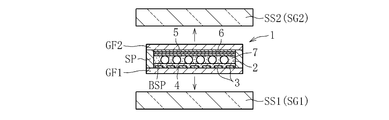
- FIG. 1 is a cross-sectional view illustrating an example of an electronic device according to the first embodiment.
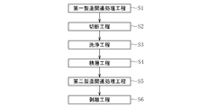
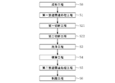
- FIG. 2 is a flowchart showing a method for manufacturing an electronic device.
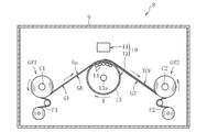
- FIG. 3 is a cross-sectional view showing the first manufacturing related processing step.
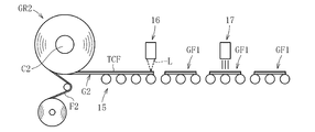
- FIG. 4 is a side view showing a cutting process and a cleaning process.
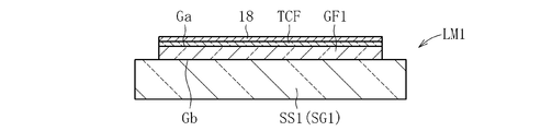
- FIG. 5A is a side view showing the stacking process.
- FIG. 5B is a side view showing the stacking process.
- FIG. 6A is a side view showing the stacking process.
- FIG. 6B is a side view showing the stacking process.
- FIG. 7 is a flowchart showing a second manufacturing-related processing step.
- FIG. 8A is a cross-sectional view showing a patterning step in the second manufacturing related processing step.
- FIG. 8A is a cross-sectional view showing a patterning step in the second manufacturing related processing step.
- FIG. 8B is a cross-sectional view showing a patterning step in the second manufacturing related processing step.
- FIG. 8C is a cross-sectional view showing a patterning step in the second manufacturing related processing step.
- FIG. 8D is a cross-sectional view showing a patterning step in the second manufacturing related processing step.
- FIG. 8E is a cross-sectional view showing a patterning step in the second manufacturing related processing step.
- FIG. 9A is a side view showing the alignment film forming step in the second manufacturing related processing step.
- FIG. 9B is a side view showing the alignment film forming step in the second manufacturing related processing step.
- FIG. 10A is a cross-sectional view illustrating an assembling process and a peeling process in the second manufacturing related processing process.
- FIG. 10B is a cross-sectional view showing an assembly process and a peeling process in the second manufacturing related processing process.
- FIG. 10C is a cross-sectional view illustrating an assembling process and a peeling process in the second manufacturing related processing process.
- FIG. 10D is a cross-sectional view showing an assembly process and a peeling process in the second manufacturing related processing process.
- FIG. 11 is a side view showing the method for manufacturing the electronic device according to the second embodiment.
- FIG. 12 is a cross-sectional view illustrating an example of an electronic device according to the third embodiment.
- FIG. 13 is a side view showing an electronic device manufacturing apparatus.
- FIG. 14 is a flowchart showing a method for manufacturing an electronic device.
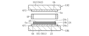
- FIG. 15A is a cross-sectional view showing an assembling process and a peeling process in the second manufacturing related processing process.
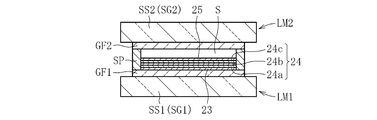
- FIG. 15B is a cross-sectional view showing an assembly process and a peeling process in the second manufacturing related processing process.
- FIG. 15C is a cross-sectional view showing an assembly process and a peeling process in the second manufacturing related processing process.
- FIG. 1 to 10 show an embodiment of a method for manufacturing an electronic device according to the present invention.
- FIG. 1 shows a liquid crystal element 1 (liquid crystal cell) as an example of an electronic device.
- the liquid crystal element 1 includes a first glass film GF1 (substrate), a second glass film GF2 (substrate), a spacer SP, and a liquid crystal layer 2 interposed between the first glass film GF1 and the second glass film GF2.
- the first glass film GF1 and the second glass film GF2 are configured in a rectangular shape, but are not limited to this shape.
- silicate glass and silica glass are used, preferably borosilicate glass, soda lime glass, aluminosilicate glass, and chemically strengthened glass, most preferably alkali-free glass. Is used.
- non-alkali glass is a glass that does not substantially contain an alkali component (alkali metal oxide), and specifically, a glass having a weight ratio of the alkali component of 3000 ppm or less. is there.
- the weight ratio of the alkali component in the present invention is preferably 1000 ppm or less, more preferably 500 ppm or less, and most preferably 300 ppm or less.
- the glass films GF1 and GF2 can be formed by a known float method, roll-out method, slot down draw method, redraw method, etc., but are preferably formed by an overflow down draw method.
- each glass film GF1, GF2 is 500 ⁇ m or less, preferably 10 ⁇ m or more and 300 ⁇ m or less, and most preferably 30 ⁇ m or more and 200 ⁇ m or less.
- the first glass film GF1 has a first electrode layer 3 (pixel electrode) constituted by a transparent conductive film TCF and a first alignment film 4 laminated on the first electrode layer 3.
- a first electrode layer 3 pixel electrode constituted by a transparent conductive film TCF and a first alignment film 4 laminated on the first electrode layer 3.
- the material of the first electrode layer 3 is not particularly limited as long as it has translucency and conductivity.
- the first electrode layer 3 is made of, for example, indium-doped tin oxide (ITO), fluorine-doped tin oxide (FTO), indium zinc oxide (IZO), aluminum-doped zinc oxide (AZO), or the like.
- the thickness of the first electrode layer 3 is preferably 10 nm or more and 1000 nm or less, more preferably 50 nm or more and 500 nm or less, and most preferably 100 nm or more and 300 nm or less.
- the sheet resistance of the first electrode layer 3 is preferably 20 ⁇ / ⁇ or less, and more preferably 15 ⁇ / ⁇ or less.
- the first alignment film 4 is, for example, a transparent film made of a polyimide film or other material in which minute grooves are formed by rubbing.
- the thickness of the first alignment film 4 is preferably 10 nm to 10 ⁇ m, more preferably 10 nm to 1 ⁇ m, and most preferably 10 nm to 500 nm.
- the liquid crystal molecules contained in the liquid crystal layer 2 can be aligned at a pretilt angle by the action of the first alignment film 4.
- the second glass film GF2 has a color filter layer 5, a second electrode layer 6 (counter electrode) composed of a transparent conductive film TCF, and a second alignment film 7.
- the color filter layer 5 includes a black matrix and a plurality of colored pixels.
- the material, thickness, and sheet resistance of the second electrode layer 6 are the same as those of the first electrode layer 3.
- the configuration, material, and thickness of the second alignment film 7 are the same as those of the first alignment film 4.
- the spacer SP is made of glass or metal, but is not limited to this material.
- the spacer SP is a seal member configured in a frame shape so as to surround the liquid crystal layer 2.
- the spacer SP has an injection port (not shown) for injecting liquid crystal inside.
- the liquid crystal layer 2 is composed of nematic liquid crystal or the like.
- the liquid crystal layer 2 is formed (sealed) in a space defined by the first glass film GF1, the second glass film GF2, and the spacer SP.
- a plurality of bead spacers BSP are provided in the liquid crystal layer 2.
- the method includes a first manufacturing related processing step S1, a cutting step S2, a cleaning step S3, a laminating step S4, a second manufacturing related processing step S5, and a peeling step S6.
- the first manufacturing related processing step S1 includes a step of forming a transparent conductive film TCF on the surface of the base material glass film G1 (film formation step) while transporting the belt-like base material glass film G1 in a predetermined direction. .
- FIG. 3 shows the film forming apparatus 8 used in the first manufacturing related processing step S1.
- the film forming apparatus 8 includes a vacuum chamber 9, a base glass roll GR 1 that winds up the base glass film G 1, a film forming unit 10, and a film that winds up the film-coated glass film G 2 after film formation.
- the base glass roll GR 1, the film forming unit 10, and the film-attached glass roll GR 2 are arranged in the vacuum chamber 9.
- the base material glass roll GR1 and the film-coated glass roll GR2 are connected by a roll-to-roll method.
- one surface is referred to as a first surface Ga, and the other surface is a second surface. It is called surface Gb.
- the base material glass roll GR1 is configured by winding a belt-shaped base material glass film G1 around the core C1.
- the base glass roll GR1 is separately prepared for the first glass film GF1 and the second glass film GF2.
- a protective film F1 made of a resin (PET or the like) is superimposed on the base glass film G1.
- the protective film F1 is separated from the base glass film G1 when the base glass film G1 is drawn from the base glass roll GR1.
- the film-coated glass roll GR2 is configured by winding the film-coated glass film G2 around the core C2.
- the glass roll with film GR2 is separately prepared for the first glass film GF1 and the second glass film GF2.
- the film forming unit 10 can form the transparent conductive film TCF on the base material glass film G1 by various film forming methods such as sputtering, vapor deposition, and CVD. In the present embodiment, a case where an ITO film as the transparent conductive film TCF is formed by a sputtering method will be described.
- the film forming unit 10 is configured by an ion beam sputtering device, a magnetron sputtering device, or the like.
- the film forming unit 10 as a sputtering apparatus mainly includes a sputtering source 11 including a target and a heating roller 12 that supports the base glass film G1.
- the sputter source 11 is arranged at a constant interval from the heating roller 12 so that sputter particles (ITO particles) scattered from the target adhere to the first surface Ga of the base glass film G1.
- the heating roller 12 includes a cylindrical roller body 13 that supports the base material glass film G ⁇ b> 1 and a heater 14 that heats the roller body 13.
- the roller body 13 is made of glass or ceramics.
- the roller body 13 is rotatably supported by the shaft portion 13a.
- the heater 14 is disposed inside the roller body 13 in order to heat the roller body 13.
- the heater 14 is comprised by an infrared heater or a near-infrared heater, for example, it is not limited to these.
- the base material glass film G1 is continuously drawn from the base material glass roll GR1 (base material glass film supplying step), and the film-forming glass film G2 is formed by passing through the film forming unit 10.
- a predetermined vacuum degree is set by a vacuum pump (not shown), and an inert gas such as argon gas is supplied.
- the film forming unit 10 scatters sputtered particles (for example, ITO particles) from the sputter source 11 and sequentially adheres them to the surface of the base material glass film G1.
- the roller body 13 of the heating roller 12 rotates in a predetermined direction (the direction of arrow R in FIG. 3) along the conveying direction of the base glass film G1 by driving the shaft portion 13a by a driving source (not shown). .
- a part of the roller body 13 is in contact with the second surface Gb of the base material glass film G1.
- the roller main body 13 guides the base glass film G1 to the downstream side by the rotation.
- the roller body 13 is heated to a predetermined temperature by the heater 14.
- the temperature of the roller body 13 is set to, for example, 200 ° C. or more and 500 ° C. or less, but is not limited to this range.
- the roller main body 13 guides the base material glass film G1 to the downstream side while heating.
- the base glass film G1 is heated to 150 ° C. or higher by the roller body 13.
- the base glass film G1 is desirably heated to 200 ° C. or higher.
- the ITO particles adhering to the base material glass film G1 are crystallized, and a transparent conductive film TCF having a low resistance (20 ⁇ / ⁇ or less) is formed.
- a strip-shaped glass film with film G2 is formed.
- the glass film with film G2 is wound up by the core C2.
- a protective film F2 is overlaid on the film-coated glass film G2 when the film is wound around the core C2.
- the film-coated glass film G2 having a predetermined length is wound around the core C2, whereby the film-coated glass roll GR2 is formed, and the first manufacturing related processing step S1 is completed. Thereafter, the glass roll with film GR ⁇ b> 2 is taken out from the vacuum chamber 9.
- the color filter layer 5 is formed on the base material glass film G1 before the film forming step. Formed (color filter forming step).
- the color filter formation process supports multiple colors (RGB) by forming a black matrix on the first surface Ga of the base glass film G1 and then repeating the color resist coating process, the exposure process, and the development / baking process.
- the color filter layer 5 to be formed is formed.
- the color filter forming step is performed in the atmosphere by a roll-to-roll method. Thereby, the base material glass roll GR1 including the color filter layer 5 is configured.
- the base material glass film G1 is drawn from the base material glass roll GR1, and the film formation step is performed on the first surface Ga of the base material glass film G1.
- the film-coated glass film G2 having the color filter layer 5 and the transparent conductive film TCF is formed.
- a film-coated glass roll GR2 for the second glass film GF2 is formed.
- the film-coated glass film G ⁇ b> 2 is pulled out from the film-coated glass roll GR ⁇ b> 2 taken out from the vacuum chamber 9, and the film-coated glass film G ⁇ b> 2 is removed by a transport device 15 including a roller conveyor. Transport (transport process).
- the film-attached glass film G2 is cut into single sheets by the cutting device 16 during conveyance.
- the cutting device 16 irradiates the laser beam L to melt or cleave the film-coated glass film G2. Not only this but the cutting device 16 can cut
- the film-coated glass film G2 is pulled out from the film-coated glass roll GR2 for the second glass film GF2, and the above-described cutting step S2 is performed, whereby the sheet-fed sheet having the color filter layer 5 and the transparent conductive film TCF is obtained.
- the second glass film GF2 is formed.
- the glass films GF1 and GF2 are continuously conveyed by the conveying device 15 continuously.
- cleaning is performed by spraying a cleaning liquid (for example, water) from the cleaning device 17 disposed on the downstream side of the cutting device 16 onto each of the glass films GF1 and GF2.
- a cleaning liquid for example, water
- the cleaning step S3 is not limited to this, and the glass films GF1 and GF2 may be cleaned with a brush or the like, or may be cleaned by immersing the glass films GF1 and GF2 in a cleaning solution.
- a drying step may be performed after the cleaning step S3.
- the drying process includes natural drying and heat drying.
- the lamination step S4 as shown in FIG. 5A, the second surface Gb of the first glass film GF1 is brought into contact with the first support substrate SS1 (first support glass SG1). Thereby, the 1st glass film laminated body LM1 shown to FIG. 5B is comprised.
- the stacking step S4 as shown in FIG. 6A, the second surface Gb of the second glass film GF2 is brought into contact with the second support substrate SS2 (second support glass SG2). Thereby, the 2nd glass film laminated body LM2 shown to FIG. 6B is comprised.
- Each support substrate SS1, SS2 (each support glass SG1, SG2) is configured in a rectangular shape, but is not limited to this shape.
- Each support substrate SS1, SS2 (each support glass SG1, SG2) desirably has a larger area than each glass film GF1, GF2.
- the thickness of each support substrate SS1, SS2 (each support glass SG1, SG2) is preferably equal to or greater than the thickness of each glass film GF1, GF2.
- its thickness is preferably 300 ⁇ m or more and 700 ⁇ m or less, and most preferably 500 ⁇ m or more and 700 ⁇ m or less.
- each support substrate SS1, SS2 various metal plates, various ceramic plates, various resin plates, and various glass plates can be used.
- each of the support substrates SS1 and SS2 is made of a resin plate.
- the material for example, an acrylic resin, a polycarbonate resin, or the like are preferably used.
- the material is silicate glass or silica glass, preferably borosilicate glass, soda lime glass, aluminosilicate. Salt glass and chemically tempered glass are used, and alkali-free glass is most preferably used.
- Each supporting glass SG1, SG2 as each supporting substrate SS1, SS2 is preferably formed by downdraw method, float method, slot downdraw method, rollout method, updraw method, redraw method, etc., overflow down More preferably, it is formed by a draw method.
- Each support glass SG1, SG2 as each support substrate SS1, SS2 is configured by cutting a strip-shaped glass plate into a sheet.
- the adhesive force between the first glass film GF1 and the first support substrate SS1 (first support glass SG1), the second glass film GF2 and the second support substrate SS2 You may provide a difference in the adhesive force with (2nd support glass SG2).
- peeling process S6 mentioned later for example, it peels so that 1st support substrate SS1 (1st support glass SG1) may be peeled, and 2nd support substrate SS2 (2nd support glass SG2) may be peeled after that. Can be controlled.
- each supporting glass SG1, SG2 when each supporting glass SG1, SG2 is used as each supporting substrate SS1, SS2, the first glass film laminated body LM1 or the second glass film laminated body LM2 after the lamination step S4. In contrast, it is preferable to perform heat treatment at a relatively low temperature (about 100 ° C. to 200 ° C.). Moreover, when using each support glass SG1, SG2 as each support substrate SS1, SS2, each support glass SG1, SG2 is subjected to a roughening treatment, and the first support substrate SS1 (first support glass SG1) and the second support substrate SS1, SS2.
- a difference may be caused in the adhesive force.
- you may make a difference in adhesive force by interposing the adhesive layer from which adhesive force differs between each support substrate SS1, SS2 (each support glass SG1, SG2) and each glass film GF1, GF2.
- a predetermined electrode pattern is formed on the transparent conductive film TCF of the glass films GF1 and GF2 (patterning step S51), and the first alignment film 4 is formed. And a step of assembling the liquid crystal element 1 (an assembly step S53).
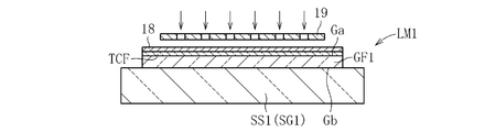
- Patterning step S51 performs a predetermined patterning process on the transparent conductive film TCF of the first glass film GF1. Specifically, first, as shown in FIG. 8A, a photoresist (photosensitive resin) is applied on the transparent conductive film TCF of the first glass film GF1 to form a resist layer 18 (resist layer forming step). ). The application of the photoresist is performed by, for example, a spin coating method, but is not limited to this method.
- the resist layer 18 is covered with a photomask 19 and irradiated with light (for example, ultraviolet rays) (exposure process). As a result, a pattern having a predetermined shape formed on the photomask 19 is transferred to the resist layer 18.
- light for example, ultraviolet rays
- a resist developer is supplied to the resist layer 18 (development process).
- a resist developer is supplied to the resist layer 18 (development process).
- the exposed portion of the resist layer 18 is removed, and a resist pattern is formed by the resist layer 18 on the transparent conductive film TCF.
- the transparent conductive film TCF is etched to remove unnecessary portions in the transparent conductive film TCF (etching process).
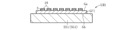
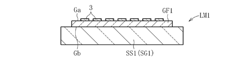
- the first electrode layer 3 having an electrode pattern made of the transparent conductive film TCF is formed on the first glass film GF1 by removing the resist layer 18 remaining on the transparent conductive film TCF (peeling step). (See FIG. 8E).
- the patterning step S51 is also performed on the transparent conductive film TCF of the second glass film GF2.
- the second glass film GF2 is used.
- the patterning step S51 may not be performed.
- the 2nd electrode layer 6 by the transparent conductive film TCF is comprised also in the 2nd glass film GF2.
- a switching element (TFT or the like) together with the first electrode layer 3 is formed on the first glass film GF1 by photolithography or other methods.
- the alignment film forming step S52 is performed.
- the alignment films 4 and 7 are formed so as to cover the electrode layers 3 and 6 of the glass films GF1 and GF2 by a spin coating method or the like. Thereafter, the alignment films 4 and 7 are rubbed. In the rubbing process, as shown in FIGS. 9A and 9B, the rubbing roller 20 is brought into contact with the surfaces of the alignment films 4 and 7. As the rubbing roller 20 rotates, innumerable minute grooves are formed on the entire surfaces of the alignment films 4 and 7.
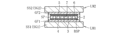
- the assembly step S53 first, as shown in FIG. 10A, the first glass film laminate LM1 and the second glass film laminate LM2 are opposed to each other, and the spacer SP and the bead spacer BSP are interposed therebetween.
- the spacer SP joins the first glass film GF1 and the second glass film GF2 with a resin adhesive.
- FIG. 10B the accommodation space S of the liquid crystal layer 2 is formed by the first glass film GF1, the spacer SP, and the second glass film GF2.
- liquid crystal is filled into the accommodation space S through the inlet of the spacer SP.
- the inlet of the spacer SP is closed (sealing process), and the liquid crystal layer 2 is formed between the first glass film GF1 and the second glass film GF2.
- the bead spacer BSP is made of a spherical resin or glass, and the thickness of the liquid crystal layer 2 is kept uniform.
- each supporting substrate SS1, SS2 (each supporting glass SG1, SG2) is peeled off from each glass film GF1, GF2 by a known peeling device having a holder such as a suction cup.
- a peeling device having a holder such as a suction cup.
- the glass films GF1, GF2 are formed after the stacking step S4 by performing the film forming step of the first manufacturing related processing step S1 before executing the stacking step S4.
- the film-coated glass film G2 can be efficiently formed, and as a result, the manufacturing efficiency of the electronic device can be increased and the manufacturing cost can be reduced.
- the heat treatment in the film forming step before the lamination step S4 it is not necessary to perform the heat treatment after the lamination step S4, and the glass films GF1, GF2 and the supporting substrates in the glass film laminates LM1, LM2 are eliminated.
- each support substrate SS1, SS2 (each support glass SG1, SG2) can be easily peeled from each glass film GF1, GF2. Further, by performing the heat treatment in the film forming step before the lamination step S4, it is not necessary to perform the heat treatment after the lamination step S4, and it is possible to use a resin plate having low heat resistance as the support substrates SS1 and SS2. It becomes.
- FIG. 11 shows a second embodiment of the present invention.
- the aspect of 1st manufacture relevant process step S1 differs from 1st embodiment.
- the transparent conductive film TCF is formed on the band-shaped base glass film G1 by the sputtering method in the vacuum chamber 9, but in the present embodiment, the first manufacturing related processing step S1 is performed by the printing method. Execute.
- FIG. 11 shows the first manufacturing related processing step S1, the cutting step S2, and the cleaning step S3 in the present embodiment.
- the first manufacturing-related processing step S1 is performed by using the printing device 21 disposed on the downstream side of the base glass roll GR1 while pulling out the base glass film G1 from the base glass roll GR1 and transporting it by the transport device 15.
- a transparent conductive film TCF is formed on the first surface Ga of the glass film G1.
- the transparent conductive film TCF formed on the base material glass film G1 is composed of, for example, a large number of nanowires composed of a metal such as silver or gold, carbon, or other materials.
- the printing device 21 forms a transparent conductive film TCF by ejecting a printing liquid containing nanowires onto the base material glass film G1 by inkjet printing. Not limited to this, the printing device 21 is not limited to this configuration, and may use screen printing, letterpress printing, gravure printing, offset printing, and gravure offset printing.
- the printing device 21 can form the first electrode layer 3 and the second electrode layer 6 having a predetermined electrode pattern. That is, the patterning step S51 executed in the second manufacturing related processing step S5 in the first embodiment is executed in the first manufacturing related processing step S1 in the present embodiment.
- the film-coated glass film G2 is cut into a sheet by the cutting device 16 disposed on the downstream side in the transport direction from the printing device 21 (cutting step S2). . Thereafter, similarly to the first embodiment, the liquid crystal element 1 is manufactured through the cleaning step S3, the stacking step S4, the second manufacturing related processing step S5 (alignment film forming step and assembly step), and the peeling step S6.
- the transparent conductive film TCF is formed by a printing method, so that it is not necessary to perform a film forming process under a vacuum environment as in the first embodiment. . Thereby, the manufacturing cost of an electronic device can be reduced further.
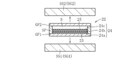
- FIG. 12 illustrates an organic EL element 22 (organic EL lighting element) as an electronic device.
- the organic EL element 22 includes a first glass film GF1, a second glass film GF2, and a spacer SP.
- the first glass film GF1 is laminated on the organic EL layer 24, the first electrode layer 23 made of the transparent conductive film TCF, the organic EL layer 24 including the hole transport layer 24a, the light emitting layer 24b, and the electron transport layer 24c.
- Second electrode layer 25 In addition to the above, the organic EL element 22 may have a hole injection layer and an electron injection layer.
- the first electrode layer 23 is configured as an anode and has a function of injecting holes into the hole transport layer 24a.
- the first electrode layer 23 is made of, for example, a transparent conductive film TCF including nanowires made of a metal such as silver or gold, carbon, or other material. Not only this but the 1st electrode layer 23 is comprised by indium dope tin oxide (ITO), fluorine dope tin oxide (FTO), indium zinc oxide (IZO), aluminum dope zinc oxide (AZO), etc. Also good.
- the hole transport layer 24a has a function of promoting hole movement to the light emitting layer 24b.
- a material for forming the hole transport layer 24a for example, bis (di (p-tolyl) aminophenyl) -1,1-cyclohexane [13], TPD [11], N, N′-diphenyl-NN -Aromatic amine derivatives including triphenyldiamines such as bis (1-naphthyl) -1,1'-biphenyl) -4,4'-diamine (NPB) [14], polyvinylcarbazole or derivatives thereof, polysilane Or derivatives thereof, polysiloxane derivatives having aromatic amines in the side chain or main chain, pyrazoline derivatives, arylamine derivatives, stilbene derivatives, triphenyldiamine derivatives, polyaniline or derivatives thereof, polythiophene or derivatives thereof, polyarylamines or derivatives thereof , Polypyrrole or derivatives
- the light emitting layer 24b is a layer containing a light emitting material, and an organic compound that mainly emits fluorescence or phosphorescence is usually used as the light emitting material. Specific examples include the following pigment materials, metal complex materials, and polymer materials. The light emitting layer 24b formed of these organic compounds may further contain a dopant material.
- dye-based materials include cyclopentamine derivatives, tetraphenylbutadiene derivative compounds, triphenylamine derivatives, oxadiazole derivatives, pyrazoloquinoline derivatives, distyrylbenzene derivatives, distyrylarylene derivatives, pyrrole derivatives, thiophene ring compounds. Pyridine ring compounds, perinone derivatives, perylene derivatives, oligothiophene derivatives, trifumanylamine derivatives, oxadiazole dimers, pyrazoline dimers, and the like.
- the metal complex material examples include metal complexes that emit light from triplet excited states such as iridium complexes and platinum complexes, aluminum quinolinol complexes, benzoquinolinol beryllium complexes, benzoxazolyl zinc complexes, and benzothiazole zinc complexes. Azomethyl zinc complex, porphyrin zinc complex, europium complex and the like.
- the central metal has Al, Zn, Be or the like or a rare earth metal such as Tb, Eu or Dy, and the ligand is oxadiazole, thiadiazole, phenylpyridine, phenylbenzo Examples thereof include metal complexes having an imidazole or quinoline structure.
- examples of the polymer material include distyrylarylene derivatives, oxadiazole derivatives, polyparaphenylene vinylene derivatives, polythiophene derivatives, polyparaphenylene derivatives, polysilane derivatives, polyacetylene derivatives, polyfluorene derivatives, polyvinylcarbazole derivatives, quinacridone Derivatives, coumarin derivatives, those obtained by polymerizing the above dye bodies and metal complex light emitting materials, that is, polymers thereof.
- the electron transport layer 24c has a function of promoting electron transfer to the light emitting layer 24b.
- Examples of the material of the electron transport layer 24c include 2- (4-biphenylyl) -5- (4-tert-butylphenyl) -1,3,4-oxadiazole (Bu-PBD) [18], OXD- Oxadiazole derivatives such as 7 [3], triazole derivatives ([19], [20], etc.), anthraquinodimethane or its derivatives, benzoquinone or its derivatives, naphthoquinone or its derivatives, anthraquinone or its derivatives, tetracyanoanthra Quinodimethane or derivatives thereof, fluorenone derivatives, diphenyldicyanoethylene or derivatives thereof, diphenoquinone derivatives, or metal complexes of 8-hydroxyquinoline or derivatives thereof, polyquinoline or derivatives thereof, polyquinoxaline or derivatives thereof, polyfluorene or Like
- the second electrode layer 25 is configured as a cathode and has a function of injecting electrons into the electron transport layer 24c.
- Examples of the material of the second electrode layer 25 include lithium, sodium, potassium, rubidium, cesium, beryllium, magnesium, calcium, strontium, barium, aluminum, scandium, vanadium, zinc, yttrium, indium, cerium, samarium, europium, and terbium.
- alloys include magnesium-silver alloys, magnesium-indium alloys, magnesium-aluminum alloys, indium-silver alloys, lithium-aluminum alloys, lithium-magnesium alloys, lithium-indium alloys, calcium-aluminum alloys, and the like. It is done.
- the second electrode layer 25 is configured as a transparent conductive film made of indium-doped tin oxide (ITO), fluorine-doped tin oxide (FTO), indium zinc oxide (IZO), aluminum-doped zinc oxide (AZO), or the like. May be.
- ITO indium-doped tin oxide
- FTO fluorine-doped tin oxide
- IZO indium zinc oxide
- AZO aluminum-doped zinc oxide
- the spacer SP is made of glass or metal, but is not limited to this material. It is a frame-shaped sealing member that seals the first electrode layer 23, the organic EL layer 24, and the second electrode layer 25 together with the first glass film GF1 and the second glass film GF2.
- FIG. 13 shows an electronic device manufacturing apparatus 26.
- the manufacturing device 26 includes a molding device 27, a transport device 15, printing devices 21a to 21e, cutting devices 16a and 16b, and a cleaning device 17.
- the forming device 27 continuously forms the strip-shaped base glass film G1 by the overflow down draw method.
- the molding device 27 includes a substantially wedge-shaped molded body 28 having an overflow groove 28a formed at the upper end thereof, and an edge roller that is disposed immediately below the molded body 28 and sandwiches molten glass overflowing from the molded body 28 from both front and back sides. 29 and an annealer 30 disposed immediately below the edge roller 29.
- the forming apparatus 27 forms the film-like molten glass by causing the molten glass overflowing from above the overflow groove 28a of the formed body 28 to flow down along both side surfaces and joining at the lower end.
- the edge roller 29 regulates the shrinkage of the molten glass in the width direction to form a base glass film G1 having a predetermined width.
- the annealer 30 is for subjecting the base material glass film G1 to distortion removal processing.
- the annealer 30 includes annealer rollers 31 arranged in a plurality of stages in the vertical direction.
- a support roller 32 is provided below the annealer 30, to hold the base glass film G1 from both the front and back sides. A tension is applied between the support roller 32 and the edge roller 29 or between the support roller 32 and any one of the annealing rollers 31 for promoting the thinning of the base glass film G1.
- a direction changing portion 33 for changing the conveying direction of the base glass film G1.
- a plurality of guide rollers 34 for guiding the base glass film G1 are arranged in a curved shape. These guide rollers 34 guide the base material glass film G1 conveyed in the vertical direction in the lateral direction.
- the conveying device 15 is arranged in front of the direction changing unit 33 in the traveling direction (downstream side).
- the transport device 15 is configured by a roller conveyor, but is not limited to this configuration.
- the printing devices 21a to 21e include a first printing device 21a that forms the first electrode layer 23, a second printing device 21b that forms the hole transport layer 24a, a third printing device 21c that forms the light emitting layer 24b, A fourth printing device 21d for forming the electron transport layer 24c and a fifth printing device 21e for forming the second electrode layer 25 are included.
- Each of the printing apparatuses 21a to 21e forms the layers 23 to 25 on the first surface Ga of the base glass film G1 by inkjet printing, screen printing, letterpress printing, gravure printing, offset printing, gravure offset printing, or the like.
- the cutting devices 16a and 16b cut the film-coated glass film G2 by laser cutting or laser cutting similarly to the cutting device 16 of the first embodiment.
- Cutting device 16a, 16b contains the 1st cutting device 16a which cut
- the first cutting device 16a is disposed on the downstream side of the fifth printing device 21e, and the second cutting device 16b is disposed on the downstream side of the first cutting device 16a.
- the cleaning device 17 is disposed on the downstream side of the second cutting device 16b.
- this method includes a molding step S0, a first manufacturing related processing step S1, a first cutting step S21, a second cutting step S22, a cleaning step S3, a laminating step S4, and a second manufacturing related processing step S5. And a peeling step S6.
- the molten glass that has overflowed from above the overflow groove 28a of the molded body 28 in the molding device 27 is caused to flow down along both side surfaces, and merged at the lower end to form a film-like molten glass.
- shrinkage in the width direction of the molten glass is regulated by the edge roller 29 to obtain a base glass glass film G1 having a predetermined width.
- the base glass film G1 is subjected to a strain removal process by the annealer 30 (slow cooling process). Due to the tension of the support roller 32, the base glass film G1 is formed to a predetermined thickness.
- the conveyance direction of the molded base material glass film G1 is converted into the horizontal direction by the direction conversion unit 33. Furthermore, the belt-shaped base material glass film G1 is transported in the lateral direction by the transport device 15 (transport process).
- Each of the printing devices 21a to 21e includes a first electrode layer 23, an organic EL layer 24 (a hole transport layer 24a, a light emitting layer 24b, an electron transport layer 24c), and a base glass film G1 transported by the transport device 15.
- the second electrode layer 25 is laminated in this order. Thereby, the strip
- the width direction end portion (ear portion) of the film-coated glass film G2 is cut and removed by the first cutting device 16a.
- membrane is cut
- the first cutting device 16a may be upstream of the first manufacturing related processing step S1 (printing device 21).
- the laminating step S4 is performed through the cleaning step S3.
- the first glass film GF1 is laminated on the first support substrate SS1 (first support glass SG1).
- a sheet-like second glass film GF2 is laminated on the second support substrate SS2 (second support glass SG2).
- the 1st glass film laminated body LM1 and the 2nd glass film laminated body LM2 are comprised (refer FIG. 15A).
- an assembly step using the first glass film laminate LM1, the second glass film laminate LM2, and the spacer SP is executed. That is, as shown to FIG. 15A, 1st glass film laminated body LM1 and 2nd glass film laminated body LM2 are made to oppose, and spacer SP is interposed between them. Then, as shown to FIG. 15B, 1st glass film GF1 and 2nd glass film GF2 are joined via spacer SP. At this time, a space S formed between the first glass film GF1 and the second glass film GF2 is filled with a sealing material such as an inert gas or a resin.
- a sealing material such as an inert gas or a resin.
- the supporting substrates SS1 and SS2 (supporting glasses SG1 and SG2) are removed from the glass films GF1 and GF2 by a peeling step S6 shown in FIG. 15C.
- the organic EL element 22 is completed.
- this invention is not limited to the structure of the said embodiment, It is not limited to the above-mentioned effect.
- the present invention can be variously modified without departing from the gist of the present invention.
- the glass films GF1 and GF2 are brought into direct contact with the support substrates SS1 and SS2 (support glasses SG1 and SG2) in the stacking step S4 is described, but the configuration is not limited thereto.
- a resin adhesive layer silicone resin, acrylic resin, or the like
- SS1 and SS2 support glasses SG1 and SG2
- SS2 each supporting glass SG1, SG2
- a resin adhesive layer When a resin adhesive layer is used, excessive amounts of the support substrates SS1 and SS2 (support glasses SG1 and SG2) and the glass films GF1 and GF2 due to the heating process (film formation process) in the first embodiment. Although adhesion problems are unlikely to occur, a resin adhesive layer may deteriorate after a high temperature process such as a film forming process. Therefore, from the viewpoint of preventing deterioration of the adhesive layer, it is preferable to perform the stacking step S4 after the heating step described above.
- each support substrate SS1, SS2 By providing the resin adhesive layer, a metal plate other than a glass plate, a ceramic plate, a resin plate, or the like can be adopted as each support substrate SS1, SS2, and the degree of freedom of selection of each support substrate SS1, SS2 is increased. improves.
- the transparent conductive film TCF is uniformly formed by the sputtering method in the first manufacturing related processing step S1, and the patterning step S51 is performed in the second manufacturing related processing step S5.
- the present invention is not limited to this configuration.
- particles dispersed from a vapor deposition source may be attached to the first surface Ga of the base glass film G1 through a shadow mask. That is, the patterning step can be executed in the first manufacturing related processing step S1 of the first embodiment.
- the film-coated glass roll GR2 may be configured by winding the film-coated glass film G2 with a separately prepared core.
- the film-coated glass film G2 may be cut into a single wafer after the patterning process is performed on the film-coated glass film G2 while the film-coated glass film G2 is drawn from the film-coated glass roll GR2.
- the method of forming the organic EL element 22 by the printing method is exemplified, but the present invention is not limited to this.
- the organic EL element 22 may be formed by a dry process such as a sputtering method or a vapor deposition method.
- the touch panel may be manufactured by the method according to the present invention.
- a first glass film GF1 and a second glass film GF2 having a sensor pattern made of a transparent conductive film TCF are opposed to each other, and both glass films GF2 and GF2 are bonded via an insulator and a spacer. Consists of.
- the electronic device formed by joining the first glass film GF1 and the second glass film GF2 with the spacer SP is shown, but the present invention is not limited to this configuration.
- the first glass film GF1 and the second glass film GF2 may be joined by a glass frit or an adhesive, or the first glass film GF1 and the second glass film GF2 may be directly welded.
- a second glass film that is a cover glass is used to secure a housing space for the organic EL element 22 between the first glass film GF1 and the second glass film GF2.
- a recess may be formed on the surface of GF2 by processing such as sandblasting. This treatment is preferably performed in the state of the second glass film laminate LM2. Thereby, the spacer SP can be omitted.
- an annealing process such as lamp annealing or laser annealing may be performed after the formation of the transparent conductive film TCF (each electrode layer 3, 23) to be a pixel electrode.
Landscapes
- Physics & Mathematics (AREA)
- Nonlinear Science (AREA)
- General Physics & Mathematics (AREA)
- Optics & Photonics (AREA)
- Engineering & Computer Science (AREA)
- Chemical & Material Sciences (AREA)
- Crystallography & Structural Chemistry (AREA)
- Theoretical Computer Science (AREA)
- Mathematical Physics (AREA)
- Manufacturing & Machinery (AREA)
- Electroluminescent Light Sources (AREA)
- Liquid Crystal (AREA)
- Laminated Bodies (AREA)
- Devices For Indicating Variable Information By Combining Individual Elements (AREA)
Abstract
本方法は、帯状のガラスフィルムG1を搬送しつつ、このガラスフィルムG1に第一製造関連処理を行う。その後、膜付ガラスフィルムG2を枚葉状に切断する。次に、枚葉状のガラスフィルムGF1,GF2に支持基板SS1,SS2(支持ガラスSG1,SG2)を積層してガラスフィルム積層体LM1,LM2を構成する。次に、ガラスフィルム積層体LM1,LM2に第二製造関連処理を行う。最後に、ガラスフィルムGF1,GF2から支持基板SS1,SS2(支持ガラスSG1,SG2)を剥離させる。
Description
本発明は、フラットパネルディスプレイ等の電子デバイスを製造する方法に関する。
近年、省スペース化の観点から、液晶ディスプレイ、有機ELディスプレイ等のフラットパネルディスプレイや薄膜電池、タッチパネル、有機EL照明といった各種電子デバイスが普及している。これらの電子デバイスでは、さらなる薄型化が要請される。この薄型化を推進するためには、電子デバイスに使用される透明基板を一層薄型化する必要がある。例えば特許文献1では、フラットパネルディスプレイ用の基板として、厚さ200μm以下のガラスフィルムが提案されている。
上述のような電子デバイスを作製するにあたり、液晶素子、有機EL素子等を構成する機能性膜をガラスフィルムに形成し、その組み立てを行う必要がある。この場合において、ガラスフィルム単体の状態では取り扱いが大変困難なものとなる。そこで、特許文献2では、支持ガラスの上にガラスフィルムを積層したガラスフィルム積層体の状態で、製造関連処理を行うことが提案されている。
従来の電子デバイスの製造方法では、ガラスフィルム積層体毎に各種の製造関連処理を行う必要があり、間欠処理運転となっていた。また、ガラスフィルム積層体の状態でガラスフィルム側に加熱を伴う製造関連処理(例えば、成膜工程、アニール工程)を行うと、支持ガラスとガラスフィルムとが接着してしまい、組み立て後に素子付ガラスフィルムから支持ガラスを剥離させることが困難になるという問題があった。
本発明は、このような事情を考慮して成されたものであり、ガラスフィルムを用いて電子デバイスを製造する場合の歩留りの向上と製造コストの低減化を技術的課題とする。
本発明は上記の課題を解決するためのものであり、帯状のガラスフィルムを搬送しつつ、第一製造関連処理を行う工程と、前記第一製造関連処理後に前記帯状のガラスフィルムを枚葉状に切断する工程と、前記枚葉状のガラスフィルムに支持基板を積層してガラスフィルム積層体を構成する工程と、前記ガラスフィルム積層体に第二製造関連処理を行う工程と、前記第二製造関連処理後に前記枚葉状のガラスフィルムから前記支持基板を剥離させる工程と、を備えることを特徴とする。
本方法によれば、ガラスフィルム積層体を構成する前に、帯状のガラスフィルムに対して第一製造関連処理を連続的に行うことで、ガラスフィルム積層体にこの第一製造関連処理を個別に行う場合と比較して、処理の作業効率を大幅に向上させ、その製造コストを可及的に低減できる。
この場合において、前記支持基板は、支持ガラスであることが望ましい。これにより、ガラスフィルムを容易に支持ガラス上に積層することができる。
この場合において、前記第一製造関連処理は、加熱処理を含むことが望ましい。これにより、第二製造関連処理後に、電子デバイスから支持基板を容易に剥離させることができる。
前記第一製造関連処理は、パターニング処理を含むことが望ましい。第一製造関連処理においてパターニング処理を実行することで、その作業効率を向上させることができ、電子デバイスの製造コストを更に低減できる。これに限らず、前記第二製造関連処理がパターニング処理を含んでいてもよい。
上記の製造方法において、前記ガラスフィルム積層体を構成する前に前記ガラスフィルムを洗浄する工程をさらに備えることが望ましい。このように、ガラスフィルムを清浄化した上でガラスフィルム積層体を構成することで、ガラスフィルムと支持基板との間への異物の混入を防止するとともに、ガラスフィルムにおいて第一製造関連処理が施された面に異物が付着した状態で第二製造関連処理が実施されるという事態をも防止できる。
本発明によれば、ガラスフィルムを用いて電子デバイスを製造する場合の歩留りの向上と製造コストの低減化を実現できる。
以下、本発明を実施するための形態について、図面を参照しながら説明する。図1乃至図10は、本発明に係る電子デバイスの製造方法の一実施形態を示す。
図1は、電子デバイスの一例として液晶素子1(液晶セル)を示す。液晶素子1は、第一ガラスフィルムGF1(基板)と、第二ガラスフィルムGF2(基板)と、スペーサSPと、第一ガラスフィルムGF1と第二ガラスフィルムGF2の間に介在する液晶層2とを備える。
第一ガラスフィルムGF1及び第二ガラスフィルムGF2は、矩形状に構成されるが、この形状に限定されない。各ガラスフィルムGF1,GF2の材質としては、ケイ酸塩ガラス、シリカガラスが用いられ、好ましくはホウ珪酸ガラス、ソーダライムガラス、アルミノ珪酸塩ガラス、化学強化ガラスが用いられ、最も好ましくは無アルカリガラスが用いられる。ガラスフィルムGF1,GF2として無アルカリガラスを使用することで、化学的に安定なガラスとすることができる。ここで、無アルカリガラスとは、アルカリ成分(アルカリ金属酸化物)が実質的に含まれていないガラスのことであって、具体的には、アルカリ成分の重量比が3000ppm以下のガラスのことである。本発明におけるアルカリ成分の重量比は、好ましくは1000ppm以下であり、より好ましくは500ppm以下であり、最も好ましくは300ppm以下である。
各ガラスフィルムGF1,GF2は、公知のフロート法、ロールアウト法、スロットダウンドロー法、リドロー法等により成形できるが、オーバーフローダウンドロー法によって成形されていることが好ましい。
各ガラスフィルムGF1,GF2の厚みは、500μm以下とされ、好ましくは10μm以上300μm以下とされ、最も好ましくは30μm以上200μm以下である。
第一ガラスフィルムGF1は、透明導電膜TCFにより構成される第一電極層3(画素電極)と、第一電極層3に積層される第一配向膜4とを有する。
第一電極層3(透明導電膜TCF)の材質としては、透光性及び導電性を有するものであれば、特に限定されない。第一電極層3は、例えば、インジウムドープスズ酸化物(ITO)、フッ素ドープスズ酸化物(FTO)、インジウム亜鉛酸化物(IZO)、アルミニウムドープ亜鉛酸化物(AZO)などにより構成される。
第一電極層3の厚みは、10nm以上1000nm以下が好ましく、50nm以上500nm以下がより好ましく、最も好ましくは、100nm以上300nm以下である。また、第一電極層3のシート抵抗は、20Ω/□以下であることが好ましく、より好ましくは、15Ω/□以下である。
第一配向膜4は、例えばラビング処理で微小な溝部が形成されたポリイミド膜その他の材料により構成される透明膜である。第一配向膜4の厚みは、10nm以上10μm以下が好ましく、10nm以上1μm以下がより好ましく、最も好ましくは、10nm以上500nm以下である。液晶層2に含まれる液晶分子は、第一配向膜4の作用によりプレチルト角で配向され得る。
第二ガラスフィルムGF2は、カラーフィルタ層5と、透明導電膜TCFにより構成される第二電極層6(対向電極)と、第二配向膜7とを有する。カラーフィルタ層5は、ブラックマトリクス及び複数の着色画素により構成される。第二電極層6の材質、厚み及びシート抵抗は、第一電極層3と同様である。第二配向膜7の構成、材質及び厚みは、第一配向膜4と同様である。
スペーサSPは、ガラス又は金属等により構成されるが、この材質に限定されない。スペーサSPは、液晶層2を囲繞するように枠形状に構成されるシール部材である。スペーサSPは、液晶を内側に注入するための注入口(図示せず)を有する。
液晶層2は、ネマティック液晶等により構成される。液晶層2は、第一ガラスフィルムGF1、第二ガラスフィルムGF2及びスペーサSPにより区画される空間に形成(封止)される。この液晶層2内には、複数のビーズスペーサBSPが設けられている。
以下、上記構成の液晶素子1を製造する方法について説明する。図2に示すように、本方法は、第一製造関連処理工程S1、切断工程S2、洗浄工程S3、積層工程S4、第二製造関連処理工程S5、及び剥離工程S6を備える。
第一製造関連処理工程S1は、帯状の母材ガラスフィルムG1を所定の方向に搬送しつつ、当該母材ガラスフィルムG1の表面に透明導電膜TCFを成膜する工程(成膜工程)を有する。
図3は、第一製造関連処理工程S1に使用される成膜装置8を示す。成膜装置8は、真空チャンバ9と、母材ガラスフィルムG1を巻き取ってなる母材ガラスロールGR1と、成膜部10と、成膜後の膜付ガラスフィルムG2を巻き取ってなる膜付ガラスロールGR2とを備える。母材ガラスロールGR1、成膜部10、及び膜付ガラスロールGR2は、真空チャンバ9内に配置される。母材ガラスロールGR1と膜付ガラスロールGR2とは、ロールトゥロール(Roll to Roll)方式により連結されている。
なお、以下の説明では、母材ガラスフィルムG1、膜付ガラスフィルムG2、及び枚葉状の各ガラスフィルムGF1,GF2において、一方の面を第一の面Gaといい、他方の面を第二の面Gbという。
母材ガラスロールGR1は、帯状の母材ガラスフィルムG1を巻芯C1に巻き取ることにより構成される。母材ガラスロールGR1は、第一ガラスフィルムGF1用、第二ガラスフィルムGF2用に、個別に用意される。母材ガラスロールGR1では、母材ガラスフィルムG1に樹脂(PET等)からなる保護フィルムF1が重ねられている。保護フィルムF1は、母材ガラスフィルムG1が母材ガラスロールGR1から引き出される際に、当該母材ガラスフィルムG1から分離される。
膜付ガラスロールGR2は、膜付ガラスフィルムG2を巻芯C2に巻き取ることによって構成される。膜付ガラスロールGR2は、第一ガラスフィルムGF1用、第二ガラスフィルムGF2用に、個別に用意される。
成膜部10は、スパッタリング法、蒸着法、CVD法等の各種成膜法により、母材ガラスフィルムG1に透明導電膜TCFを形成できる。本実施形態では、スパッタリング法により透明導電膜TCFとしてのITO膜を形成する場合について説明する。成膜部10は、イオンビームスパッタ装置やマグネトロンスパッタ装置などにより構成される。スパッタ装置としての成膜部10は、ターゲットを含むスパッタ源11と、母材ガラスフィルムG1を支持する加熱ローラ12とを主に備える。
スパッタ源11は、ターゲットから飛散するスパッタ粒子(ITO粒子)が母材ガラスフィルムG1の第一の面Gaに付着するように、加熱ローラ12から一定の間隔をおいて配置される。加熱ローラ12は、母材ガラスフィルムG1を支持する円筒状のローラ本体13と、このローラ本体13を加熱するヒータ14とを備える。ローラ本体13は、ガラス又はセラミックスにより構成される。ローラ本体13は、軸部13aにより回転自在に支持される。ヒータ14は、ローラ本体13を加熱すべく、当該ローラ本体13の内側に配置される。ヒータ14は、例えば赤外線ヒータ又は近赤外線ヒータにより構成されるが、これらに限定されるものではない。
第一製造関連処理工程S1では、母材ガラスロールGR1から母材ガラスフィルムG1を連続的に引き出すとともに(母材ガラスフィルム供給工程)、成膜部10を通過させて膜付ガラスフィルムG2を形成する。真空チャンバ9内では、図示しない真空ポンプによって所定の真空度に設定されるとともに、アルゴンガス等の不活性ガスが供給される。成膜部10は、スパッタ源11からスパッタ粒子(例えばITO粒子)を飛散させ、母材ガラスフィルムG1の表面に順次付着させる。
加熱ローラ12のローラ本体13は、図示しない駆動源により軸部13aを駆動することで、母材ガラスフィルムG1の搬送方向に沿うように所定の方向(図3における矢印Rの方向)に回転する。ローラ本体13の一部は、母材ガラスフィルムG1の第二の面Gbに接触している。ローラ本体13は、その回転により、母材ガラスフィルムG1を下流側に案内する。
ローラ本体13は、ヒータ14によって所定の温度に加熱されている。ローラ本体13の温度は、例えば200℃以上500℃以下に設定されるが、この範囲に限定されない。これにより、ローラ本体13は、母材ガラスフィルムG1を加熱しながら下流側に案内する。母材ガラスフィルムG1は、ローラ本体13によって150℃以上に加熱される。スパッタ粒子がITOである場合、母材ガラスフィルムG1は、200℃以上に加熱されることが望ましい。母材ガラスフィルムG1によって加熱されることで、当該母材ガラスフィルムG1に付着したITO粒子が結晶化し、低抵抗(20Ω/□以下)の透明導電膜TCFが形成される。以上により、帯状の膜付ガラスフィルムG2が形成される。
膜付ガラスフィルムG2は、巻芯C2によって巻き取られる。この膜付ガラスフィルムG2には、巻芯C2に巻き取られる際に保護フィルムF2が重ねられる。所定長さの膜付ガラスフィルムG2が巻芯C2に巻き取られることで、膜付ガラスロールGR2が形成され、第一製造関連処理工程S1が終了する。その後、膜付ガラスロールGR2は、真空チャンバ9から取り出される。
なお、第二ガラスフィルムGF2用の膜付ガラスロールGR2を形成する場合には、第一製造関連処理工程S1において、上記の成膜工程の前に、母材ガラスフィルムG1にカラーフィルタ層5が形成される(カラーフィルタ形成工程)。カラーフィルタ形成工程は、母材ガラスフィルムG1の第一の面Gaに、ブラックマトリクスを形成した後、カラーレジスト塗布工程、露光工程、現像・ベーキング工程を繰り返すことにより、複数色(RGB)に対応するカラーフィルタ層5を形成する。カラーフィルタ形成工程は、大気中において、ロールトゥロール方式により実行される。これにより、カラーフィルタ層5を含む母材ガラスロールGR1が構成される。第一製造関連処理工程S1では、この母材ガラスロールGR1から母材ガラスフィルムG1が引き出され、当該母材ガラスフィルムG1の第一の面Gaに上記の成膜工程が行われる。これにより、カラーフィルタ層5及び透明導電膜TCFを有する膜付ガラスフィルムG2が形成される。この膜付ガラスフィルムG2を巻芯C2に巻き取ることで、第二ガラスフィルムGF2用の膜付ガラスロールGR2が形成される。
図4に示すように、切断工程S2では、真空チャンバ9から取り出された膜付ガラスロールGR2から膜付ガラスフィルムG2を引き出すとともに、当該膜付ガラスフィルムG2をローラコンベア等からなる搬送装置15によって搬送する(搬送工程)。膜付ガラスフィルムG2は、搬送中に切断装置16によって枚葉状に切断される。切断装置16は、レーザ光Lを照射して膜付ガラスフィルムG2を溶断又は割断する。これに限らず、切断装置16は、スクライブカッタ等の切断具により膜付ガラスフィルムG2を切断できる。これにより、透明導電膜TCFを有する枚葉状の第一ガラスフィルムGF1が形成される。
同様に、第二ガラスフィルムGF2用の膜付ガラスロールGR2から、膜付ガラスフィルムG2を引き出すとともに、上記の切断工程S2を実行することで、カラーフィルタ層5及び透明導電膜TCFを有する枚葉状の第二ガラスフィルムGF2が形成される。各ガラスフィルムGF1,GF2は、引き続き搬送装置15によって連続的に搬送される。
なお、切断工程S2では、膜付ガラスロールGR2から膜付ガラスフィルムG2が引き出される際に、当該膜付ガラスフィルムG2に重ねられていた保護フィルムF2が分離される。
洗浄工程S3は、例えば、切断装置16の下流側に配置される洗浄装置17から洗浄液(例えば水等)を各ガラスフィルムGF1,GF2に噴射することにより洗浄を行う。これに限らず、洗浄工程S3は、ブラシ等で各ガラスフィルムGF1,GF2をこするように洗浄しても良く、各ガラスフィルムGF1,GF2を洗浄液に浸漬することにより洗浄してもよい。洗浄工程S3後に、乾燥工程が実施されてもよい。乾燥工程は、自然乾燥、加熱乾燥を含む。
積層工程S4では、図5Aに示すように、第一ガラスフィルムGF1の第二の面Gbを第一支持基板SS1(第一支持ガラスSG1)に接触させる。これにより、図5Bに示す第一ガラスフィルム積層体LM1が構成される。また、積層工程S4では、図6Aに示すように、第二ガラスフィルムGF2の第二の面Gbを第二支持基板SS2(第二支持ガラスSG2)に接触させる。これにより、図6Bに示す第二ガラスフィルム積層体LM2が構成される。
各支持基板SS1,SS2(各支持ガラスSG1,SG2)は、矩形状に構成されるが、この形状に限定されない。各支持基板SS1,SS2(各支持ガラスSG1,SG2)は、各ガラスフィルムGF1,GF2よりも大きな面積を有することが望ましい。各支持基板SS1,SS2(各支持ガラスSG1,SG2)の厚みは、各ガラスフィルムGF1,GF2の厚み以上であることが好ましい。各支持基板SS1,SS2として各支持ガラスSG1,SG2を使用する場合において、その厚みは、300μm以上700μm以下であることが好ましく、500μm以上700μm以下であることが最も好ましい。
各支持基板SS1,SS2としては、各種金属板、各種セラミック板、各種樹脂板、各種ガラス板を用いることができる。第二製造関連処理S5が加熱を伴わない場合においては、各支持基板SS1,SS2を樹脂板により構成することが好適であり、その場合、その材質としては、例えばアクリル系樹脂、ポリカーボネート系樹脂等が好適に用いられる。各支持基板SS1,SS2をガラス板(各支持ガラスSG1,SG2)により構成する場合、その材質としては、ケイ酸塩ガラス、シリカガラスが用いられ、好ましくはホウ珪酸ガラス、ソーダライムガラス、アルミノ珪酸塩ガラス、化学強化ガラスが用いられ、最も好ましくは無アルカリガラスが用いられる。
各支持基板SS1,SS2としての各支持ガラスSG1,SG2は、ダウンドロー法、フロート法、スロットダウンドロー法、ロールアウト法、アップドロー法、リドロー法等によって成形されていることが好ましく、オーバーフローダウンドロー法によって成形されていることがより好ましい。各支持基板SS1,SS2としての各支持ガラスSG1,SG2は、帯状のガラス板を枚葉状に切断することにより構成される。
積層工程S4では、各ガラスフィルム積層体LM1,LM2において、第一ガラスフィルムGF1と第一支持基板SS1(第一支持ガラスSG1)との接着力と、第二ガラスフィルムGF2と第二支持基板SS2(第二支持ガラスSG2)との接着力とに差を設けてもよい。これにより、後述する剥離工程S6において、例えば、第一支持基板SS1(第一支持ガラスSG1)を剥離させ、その後に第二支持基板SS2(第二支持ガラスSG2)を剥離させるというように、剥離の順を制御できる。
接着力に差を付与する方法としては、各支持基板SS1,SS2として各支持ガラスSG1,SG2を使用する場合において、積層工程S4後に、第一ガラスフィルム積層体LM1又は第二ガラスフィルム積層体LM2に対して、比較的低温(100℃~200℃程度)の加熱処理を行うことが好ましい。また、各支持基板SS1,SS2として各支持ガラスSG1,SG2を使用する場合において、各支持ガラスSG1,SG2に粗面化処理を行い、第一支持基板SS1(第一支持ガラスSG1)と第二支持基板SS2(第二支持ガラスSG2)の表面粗さRaに差を与えることで、接着力に差を生じさせてもよい。また、各支持基板SS1,SS2(各支持ガラスSG1,SG2)と各ガラスフィルムGF1,GF2との間に接着力の異なる接着層を介在させることで、接着力に差を生じさせてもよい。
図7に示すように、第二製造関連処理工程S5は、各ガラスフィルムGF1,GF2の透明導電膜TCFに所定の電極パターンを形成する工程(パターニング工程S51)と、第一配向膜4を形成する工程(配向膜形成工程S52)と、液晶素子1を組み立てる工程(組立工程S53)とを有する。
パターニング工程S51は、第一ガラスフィルムGF1の透明導電膜TCFに、所定のパターニング処理を施す。具体的には、まず、図8Aに示すように、第一ガラスフィルムGF1の透明導電膜TCF上に、フォトレジスト(光感光性樹脂)を塗布してレジスト層18を形成する(レジスト層形成工程)。フォトレジストの塗布は、例えばスピンコート法により行われるが、この方法に限定されない。
次に、図8Bに示すように、レジスト層18にフォトマスク19を被せて光(例えば紫外線)を照射する(露光工程)。これにより、フォトマスク19に形成された所定形状のパターンがレジスト層18に転写される。
その後、レジスト層18にレジスト現像液を供給する(現像工程)。例えばポジ型レジスト層を用いた場合は、図8Cに示すように、レジスト層18の露光部分が除去され、透明導電膜TCF上にレジスト層18によるレジストパターンが形成される。
そして、図8Dに示すように、透明導電膜TCFに対してエッチング処理を行い、当該透明導電膜TCFにおける不要部分を除去する(エッチング工程)。最後に、透明導電膜TCF上に残存していたレジスト層18を除去すること(剥離工程)により、第一ガラスフィルムGF1上に、透明導電膜TCFによる電極パターンを有する第一電極層3が形成される(図8E参照)。
液晶素子1が単純マトリクス駆動型である場合、第二ガラスフィルムGF2の透明導電膜TCFにも上記のパターニング工程S51が実施されるが、アクティブマトリクス駆動型である場合には、第二ガラスフィルムGF2にはパターニング工程S51が実施されなくてもよい。これにより、第二ガラスフィルムGF2にも透明導電膜TCFによる第二電極層6が構成される。なお、アクティブマトリクス駆動型の液晶素子1の場合には、第一電極層3とともにスイッチング素子(TFT等)がフォトリソグラフィその他の方法により第一ガラスフィルムGF1に形成される。
その後、配向膜形成工程S52が実行される。各配向膜4,7は、スピンコート法等によって、各ガラスフィルムGF1,GF2の各電極層3,6を被覆するように形成される。その後、各配向膜4,7には、ラビング処理が行われる。ラビング処理は、図9A,図9Bに示すように、各配向膜4,7の表面にラビングローラ20を接触させる。ラビングローラ20の回転により、各配向膜4,7の表面全体に無数の微小な溝部が形成される。
組立工程S53では、まず図10Aに示すように、第一ガラスフィルム積層体LM1と第二ガラスフィルム積層体LM2とを対向させるとともに、その間にスペーサSP、およびビーズスペーサBSPを介在させる。スペーサSPは、樹脂製の接着剤により、第一ガラスフィルムGF1と第二ガラスフィルムGF2とを接合する。これにより、図10Bに示すように、第一ガラスフィルムGF1、スペーサSPおよび第二ガラスフィルムGF2によって、液晶層2の収容空間Sが形成される。その後、図10Cに示すように、スペーサSPの注入口を通じてこの収容空間Sに液晶が充填される。液晶の充填が終了すると、スペーサSPの注入口が閉塞され(封止工程)、第一ガラスフィルムGF1と第二ガラスフィルムGF2の間に液晶層2が形成される。なお、ビーズスペーサBSPは、球状の樹脂もしくはガラスからなり、液晶層2の厚みが均一になるように保っている。
その後、図10Dに示すように、剥離工程S6が実施される。剥離工程S6は、吸盤等の保持具を有する公知の剥離装置により、各支持基板SS1,SS2(各支持ガラスSG1,SG2)を各ガラスフィルムGF1,GF2から引き剥がす。以上により、液晶素子1が完成する。
以上説明した本実施形態による電子デバイスの製造方法によれば、積層工程S4を実行する前に第一製造関連処理工程S1の成膜工程を行うことで、積層工程S4後に各ガラスフィルムGF1,GF2に加熱成膜を行う場合と比較して、膜付ガラスフィルムG2を効率良く形成でき、結果として、電子デバイスの製造効率を高め、製造コストを低減できる。また、成膜工程における加熱処理を積層工程S4前に行うことで、積層工程S4以降に加熱処理を行う必要が無くなり、各ガラスフィルム積層体LM1,LM2における各ガラスフィルムGF1,GF2と各支持基板SS1,SS2(各支持ガラスSG1,SG2)との過剰な接着を未然に防止できる。これにより、第二製造関連処理工程S5後に、各ガラスフィルムGF1,GF2から各支持基板SS1,SS2(各支持ガラスSG1,SG2)を容易に剥離させることができる。また、成膜工程における加熱処理を積層工程S4前に行うことで、積層工程S4以降に加熱処理を行う必要が無くなり、各支持基板SS1,SS2として耐熱性の低い樹脂板を使用することが可能となる。
図11は、本発明の第二実施形態を示す。本実施形態では、第一製造関連処理工程S1の態様が第一実施形態と異なる。上記の第一実施形態では、真空チャンバ9内でスパッタリング法により帯状の母材ガラスフィルムG1に透明導電膜TCFを形成していたが、本実施形態は、印刷法によって第一製造関連処理工程S1を実行する。
図11は、本実施形態における第一製造関連処理工程S1、切断工程S2及び洗浄工程S3を示す。第一製造関連処理工程S1は、母材ガラスロールGR1から母材ガラスフィルムG1を引き出して搬送装置15により搬送しつつ、母材ガラスロールGR1の下流側に配置される印刷装置21により、母材ガラスフィルムG1の第一の面Gaに透明導電膜TCFを形成する。母材ガラスフィルムG1に形成される透明導電膜TCFは、例えば、銀、金等の金属やカーボンその他の材料により構成される多数のナノワイヤにより構成される。
印刷装置21は、インクジェット印刷により、母材ガラスフィルムG1にナノワイヤを含む印刷液を噴射して透明導電膜TCFを形成する。これに限らず、印刷装置21は、この構成に限らず、スクリーン印刷、凸版印刷、グラビア印刷、オフセット印刷、グラビアオフセット印刷を利用するものであってもよい。印刷装置21は、所定の電極パターンを有する第一電極層3及び第二電極層6を形成できる。すなわち、第一実施形態では第二製造関連処理工程S5で実行されたパターニング工程S51を、本実施形態では第一製造関連処理工程S1において実行する。
印刷装置21によって透明導電膜TCFが形成されると、膜付ガラスフィルムG2は、当該印刷装置21よりも搬送方向下流側に配置される切断装置16によって枚葉状に切断される(切断工程S2)。その後、第一実施形態と同様に、洗浄工程S3、積層工程S4、第二製造関連処理工程S5(配向膜形成工程及び組立工程)、剥離工程S6を経て液晶素子1が製造される。
以上のように、本実施形態に係る電子デバイスの製造方法では、印刷法によって透明導電膜TCFを形成することで、第一実施形態のような真空環境下での成膜工程を行う必要がない。これにより、電子デバイスの製造コストをより一層低減できる。
図12乃至図15は、本発明の第三実施形態を示す。図12は、電子デバイスとしての有機EL素子22(有機EL照明素子)を例示する。有機EL素子22は、第一ガラスフィルムGF1と、第二ガラスフィルムGF2と、スペーサSPとを有する。第一ガラスフィルムGF1は、透明導電膜TCFからなる第一電極層23と、正孔輸送層24a、発光層24b及び電子輸送層24cを含む有機EL層24と、この有機EL層24に積層される第二電極層25と、を有する。また、上記のほかに、有機EL素子22は、正孔注入層、電子注入層を有しても良い。
第一電極層23は、陽極として構成されており、正孔を正孔輸送層24aに注入する機能を有する。第一電極層23は、例えば、銀、金等の金属やカーボンその他の材料により構成されるナノワイヤを含む透明導電膜TCFにより構成される。これに限らず、第一電極層23は、インジウムドープスズ酸化物(ITO)、フッ素ドープスズ酸化物(FTO)、インジウム亜鉛酸化物(IZO)、アルミニウムドープ亜鉛酸化物(AZO)などにより構成されてもよい。
正孔輸送層24aは、発光層24bへの正孔移動を促進する機能を有する。正孔輸送層24aを形成する材料としては、例えば、ビス(ジ(p-トリル)アミノフェニル)-1,1-シクロヘキサン[13]、TPD[11]、N,N'-ジフェニル-N-N-ビス(1-ナフチル)-1,1'-ビフェニル)-4,4'-ジアミン(NPB)[14]等のトリフェニルジアミン類をはじめとする芳香族アミン誘導体、ポリビニルカルバゾール若しくはその誘導体、ポリシラン若しくはその誘導体、側鎖若しくは主鎖に芳香族アミンを有するポリシロキサン誘導体、ピラゾリン誘導体、アリールアミン誘導体、スチルベン誘導体、トリフェニルジアミン誘導体、ポリアニリン若しくはその誘導体、ポリチオフェン若しくはその誘導体、ポリアリールアミン若しくはその誘導体、ポリピロール若しくはその誘導体、ポリ(p-フェニレンビニレン)若しくはその誘導体、またはポリ(2,5-チエニレンビニレン)若しくはその誘導体などが挙げられる。
発光層24bは、発光材料を含む層であり、通常、主として蛍光またはりん光を発する有機化合物が発光材料として用いられる。具体的には、以下の色素系材料、金属錯体系材料、高分子系材料などを挙げることができる。なお、これら有機化合物で形成される発光層24bには、ドーパント材料がさらに含まれていてもよい。
色素系材料としては、例えば、シクロペンダミン誘導体、テトラフェニルブタジエン誘導体化合物、トリフェニルアミン誘導体、オキサジアゾール誘導体、ピラゾロキノリン誘導体、ジスチリルベンゼン誘導体、ジスチリルアリーレン誘導体、ピロール誘導体、チオフェン環化合物、ピリジン環化合物、ペリノン誘導体、ペリレン誘導体、オリゴチオフェン誘導体、トリフマニルアミン誘導体、オキサジアゾールダイマー、ピラゾリンダイマーなどが挙げられる。また、金属錯体系材料としては、例えば、イリジウム錯体、白金錯体等の三重項励起状態からの発光を有する金属錯体、アルミキノリノール錯体、ベンゾキノリノールベリリウム錯体、ベンゾオキサゾリル亜鉛錯体、ベンゾチアゾール亜鉛錯体、アゾメチル亜鉛錯体、ポルフィリン亜鉛錯体、ユーロピウム錯体などを挙げることができる。さらに金属錯体系材料の他の例として、中心金属に、Al、Zn、BeなどまたはTb、Eu、Dyなどの希土類金属を有し、配位子にオキサジアゾール、チアジアゾール、フェニルピリジン、フェニルベンゾイミダゾール、キノリン構造などを有する金属錯体などを挙げることができる。あるいは、高分子系材料としては、例えば、ジスチリルアリーレン誘導体、オキサジアゾール誘導体、ポリパラフェニレンビニレン誘導体、ポリチオフェン誘導体、ポリパラフェニレン誘導体、ポリシラン誘導体、ポリアセチレン誘導体、ポリフルオレン誘導体、ポリビニルカルバゾール誘導体、キナクリドン誘導体、クマリン誘導体、上記色素体や金属錯体系発光材料などを高分子化したもの、すなわちこれらの重合体などが挙げられる。
電子輸送層24cは、発光層24bへの電子移動を促進する機能を有する。電子輸送層24cの材質としては、例えば、2-(4-ビフェニリル)-5-(4-t-ブチルフェニル)-1,3,4-オキサジアゾール(Bu-PBD)[18]、OXD-7[3]等のオキサジアゾール誘導体、トリアゾール誘導体([19]、[20]等)、アントラキノジメタン若しくはその誘導体、ベンゾキノン若しくはその誘導体、ナフトキノン若しくはその誘導体、アントラキノン若しくはその誘導体、テトラシアノアンスラキノジメタン若しくはその誘導体、フルオレノン誘導体、ジフェニルジシアノエチレン若しくはその誘導体、ジフェノキノン誘導体、または8-ヒドロキシキノリン若しくはその誘導体の金属錯体、ポリキノリン若しくはその誘導体、ポリキノキサリン若しくはその誘導体、ポリフルオレン若しくはその誘導体等が挙げられる。
第二電極層25は、陰極として構成されており、電子輸送層24cに電子を注入する機能を有する。第二電極層25の材質としては、例えばリチウム、ナトリウム、カリウム、ルビジウム、セシウム、ベリリウム、マグネシウム、カルシウム、ストロンチウム、バリウム、アルミニウム、スカンジウム、バナジウム、亜鉛、イットリウム、インジウム、セリウム、サマリウム、ユーロピウム、テルビウム、イッテルビウム、金、銀、白金、銅、マンガン、チタン、コバルト、ニッケル、タングステン、錫などのアルカリ金属やアルカリ土類金属、遷移金属、又はこれら金属を少なくとも一種類以上含む合金、またはグラファイト若しくはグラファイト層間化合物等が挙げられる。合金の例としては、例えば、マグネシウム-銀合金、マグネシウム-インジウム合金、マグネシウム-アルミニウム合金、インジウム-銀合金、リチウム-アルミニウム合金、リチウム-マグネシウム合金、リチウム-インジウム合金、カルシウム-アルミニウム合金などが挙げられる。また、第二電極層25は、インジウムドープスズ酸化物(ITO)、フッ素ドープスズ酸化物(FTO)、インジウム亜鉛酸化物(IZO)、アルミニウムドープ亜鉛酸化物(AZO)などによる透明導電膜として構成されてもよい。
スペーサSPは、ガラス又は金属等により構成されるが、この材質に限定されない。第一ガラスフィルムGF1と第二ガラスフィルムGF2とともに、第一電極層23、有機EL層24及び第二電極層25を封止する枠形状のシール部材である。
図13は、電子デバイスの製造装置26を示す。この製造装置26は、成形装置27と、搬送装置15と、印刷装置21a~21eと、切断装置16a,16bと、洗浄装置17とを備える。
成形装置27は、オーバーフローダウンドロー法により帯状の母材ガラスフィルムG1を連続的に成形する。成形装置27は、上端部にオーバーフロー溝28aが形成された断面視略楔形の成形体28と、成形体28の直下に配置されて、成形体28から溢出した溶融ガラスを表裏両側から挟むエッジローラ29と、このエッジローラ29の直下に配備されるアニーラ30とを備える。
成形装置27は、成形体28のオーバーフロー溝28aの上方から溢流した溶融ガラスを、両側面に沿ってそれぞれ流下させ、下端で合流させてフィルム状の溶融ガラスを成形する。エッジローラ29は、溶融ガラスの幅方向収縮を規制して所定幅の母材ガラスフィルムG1とする。アニーラ30は、母材ガラスフィルムG1に対して除歪処理を施すためのものである。このアニーラ30は、上下方向複数段に配設されたアニーラローラ31を有する。
アニーラ30の下方には、母材ガラスフィルムG1を表裏両側から挟持する支持ローラ32が配設されている。支持ローラ32とエッジローラ29との間、または支持ローラ32と何れか一箇所のアニーラローラ31との間では、母材ガラスフィルムG1を薄肉にすることを助長するための張力が付与されている。
支持ローラ32の下方には、母材ガラスフィルムG1の搬送方向を変換する方向変換部33が設けられる。方向変換部33には、母材ガラスフィルムG1を案内する複数のガイドローラ34が湾曲状に配列されている。これらのガイドローラ34は、鉛直方向に搬送される母材ガラスフィルムG1を横方向へと案内する。
搬送装置15は、方向変換部33の進行方向前方(下流側)に配置される。搬送装置15は、ローラコンベアにより構成されるが、この構成に限定されない。
印刷装置21a~21eは、第一電極層23を形成する第一印刷装置21aと、正孔輸送層24aを形成する第二印刷装置21bと、発光層24bを形成する第三印刷装置21cと、電子輸送層24cを形成する第四印刷装置21dと、第二電極層25を形成する第五印刷装置21eとを含む。各印刷装置21a~21eは、インクジェット印刷、スクリーン印刷、凸版印刷、グラビア印刷、オフセット印刷、グラビアオフセット印刷などにより、母材ガラスフィルムG1の第一の面Gaに各層23~25を形成する。
切断装置16a,16bは、第一実施形態の切断装置16と同様に、レーザ溶断又はレーザ割断により膜付ガラスフィルムG2を切断する。切断装置16a,16bは、母材ガラスフィルムG1の幅方向端部(耳部)を切断する第一切断装置16aと、膜付ガラスフィルムG2を枚葉状に切断する第二切断装置16bとを含む。第一切断装置16aは、第五印刷装置21eの下流側に配置されており、第二切断装置16bは、第一切断装置16aの下流側に配置されている。
洗浄装置17は、第二切断装置16bの下流側に配置される。洗浄装置17は、第一実施形態、第二実施形態と、同様に搬送装置15により搬送される第一ガラスフィルムGF1を洗浄液により洗浄する。
以下、本実施形態における電子デバイスの製造方法について説明する。図14に示すように、本方法は、成形工程S0、第一製造関連処理工程S1、第一切断工程S21、第二切断工程S22、洗浄工程S3、積層工程S4、第二製造関連処理工程S5、及び剥離工程S6を備える。
成形工程S0では、成形装置27における成形体28のオーバーフロー溝28aの上方から溢流した溶融ガラスを、両側面に沿ってそれぞれ流下させ、下端で合流させてフィルム状の溶融ガラスとする。この際、溶融ガラスの幅方向収縮をエッジローラ29により規制して所定幅の母材ガラスフィルムG1とする。その後、母材ガラスフィルムG1に対してアニーラ30により除歪処理を施す(徐冷工程)。支持ローラ32の張力により、母材ガラスフィルムG1は所定の厚みに形成される。
成形された母材ガラスフィルムG1は、方向変換部33によってその搬送方向が横方向に変換される。さらに、帯状の母材ガラスフィルムG1は、搬送装置15によって横方向に搬送される(搬送工程)。
その後、この母材ガラスフィルムG1に対して第一製造関連処理工程S1が実行される。各印刷装置21a~21eは、搬送装置15によって搬送される母材ガラスフィルムG1に、第一電極層23、有機EL層24(正孔輸送層24a、発光層24b、電子輸送層24c)、及び第二電極層25をこの順に積層形成する。これにより、帯状の膜付ガラスフィルムG2が形成される。
第一切断工程S21では、第一切断装置16aによって、膜付ガラスフィルムG2の幅方向端部(耳部)が切断除去される。その後、第二切断工程S22において、第二切断装置16bにより膜付ガラスフィルムG2を枚葉状に切断する。これにより、第一ガラスフィルムGF1が形成される。尚、第一切断装置16aは、第一製造関連処理工程S1(印刷装置21)よりも上流でも良い。
その後、洗浄工程S3を経て積層工程S4が実施される。積層工程S4では、第一支持基板SS1(第一支持ガラスSG1)に第一ガラスフィルムGF1が積層される。また、第二支持基板SS2(第二支持ガラスSG2)に枚葉状の第二ガラスフィルムGF2が積層される。これにより、第一ガラスフィルム積層体LM1及び第二ガラスフィルム積層体LM2が構成される(図15A参照)。
第二製造関連処理工程S5では、第一ガラスフィルム積層体LM1、第二ガラスフィルム積層体LM2及びスペーサSPによる組立工程を実行する。すなわち、図15Aに示すように、第一ガラスフィルム積層体LM1と第二ガラスフィルム積層体LM2とを対向させ、その間にスペーサSPを介在させる。その後、図15Bに示すように、スペーサSPを介して第一ガラスフィルムGF1と第二ガラスフィルムGF2とを接合する。この際、第一ガラスフィルムGF1と第二ガラスフィルムGF2との間に形成される空間Sに、不活性ガスや樹脂等の封止材が充填される。その後、図15Cに示す剥離工程S6により、各ガラスフィルムGF1,GF2から各支持基板SS1,SS2(各支持ガラスSG1,SG2)が取り除かれる。以上により、有機EL素子22が完成する。
なお、本発明は、上記実施形態の構成に限定されるものではなく、上記した作用効果に限定されるものでもない。本発明は、本発明の要旨を逸脱しない範囲で種々の変更が可能である。
上記の実施形態では、積層工程S4において、各ガラスフィルムGF1,GF2を各支持基板SS1,SS2(各支持ガラスSG1,SG2)に直接接触させる例を示したが、この構成に限定されない。例えば、樹脂製の接着層(シリコーン樹脂やアクリル樹脂等)を支持基板SS1,SS2(支持ガラスSG1,SG2)上に設けて、この接着層を介して各ガラスフィルムGF1,GF2を各支持基板SS1,SS2(各支持ガラスSG1,SG2)に積層させてもよい。樹脂製の接着層を使用する場合、第一実施形態における加熱工程(成膜工程)に起因する各支持基板SS1,SS2(各支持ガラスSG1,SG2)と各ガラスフィルムGF1,GF2との過剰な接着の問題は生じ難いが、樹脂製の接着層では成膜工程等の高温工程を経ると劣化するおそれがある。したがって、接着層の劣化を防止するという観点から、上述の加熱工程を経た後に積層工程S4を行うことが好ましい。樹脂製の接着層を設けることで、各支持基板SS1,SS2として、ガラス板以外の金属板やセラミック板、樹脂板等を採用することができ、各支持基板SS1,SS2の選択の自由度が向上する。
上記の第一実施形態では、第一製造関連処理工程S1において、スパッタリング法により透明導電膜TCFを一様に形成し、第二製造関連処理工程S5において、パターニング工程S51を実施する例を示したが、本発明はこの構成に限定されない。例えば、蒸着法を利用して、蒸着源から離散した粒子を、シャドーマスクを介して母材ガラスフィルムG1の第一の面Gaに付着させてもよい。すなわち、第一実施形態の第一製造関連処理工程S1においてパターニング工程を実行できる。
上記の第二実施形態では、母材ガラスロールGR1から引き出した母材ガラスフィルムG1に透明導電膜TCFを形成した後に、膜付ガラスフィルムG2を切断する例を示したが、本発明はこの態様に限定されない。例えば、ロールトゥロール方式を採用し、膜付ガラスフィルムG2を別途用意される巻芯により巻き取って膜付ガラスロールGR2を構成してもよい。この場合、膜付ガラスロールGR2から膜付ガラスフィルムG2を引き出しつつ、当該膜付ガラスフィルムG2にパターニング処理を実施し、その後に、当該膜付ガラスフィルムG2を枚葉状に切断してもよい。
上記の第三実施形態では、印刷法によって有機EL素子22を形成する方法を例示したが、本発明はこれに限定されない。有機EL素子22は、スパッタリング法、蒸着法等のドライプロセスにより形成されてもよい。
上記の実施形態では、電子デバイスとしては、液晶素子1、有機EL素子22を製造する場合を例示したが、本発明はこれらに限定されない。例えば、本発明に係る方法により、タッチパネルを製造してもよい。例えば、抵抗膜式のタッチパネルは、透明導電膜TCFによるセンサパターンを有する第一ガラスフィルムGF1及び第二ガラスフィルムGF2を対向させ、絶縁体及びスペーサを介して両ガラスフィルムGF2,GF2を接合することにより構成される。
上記の実施形態では、第一ガラスフィルムGF1と第二ガラスフィルムGF2とをスペーサSPによって接合してなる電子デバイスを示したが、本発明はこの構成に限定されない。スペーサSPに替えて、ガラスフリットや接着剤により第一ガラスフィルムGF1と第二ガラスフィルムGF2とを接合してもよく、第一ガラスフィルムGF1と第二ガラスフィルムGF2とを直接溶着させてもよい。また、電子デバイスが有機EL素子22である場合には、第一ガラスフィルムGF1と第二ガラスフィルムGF2との間に有機EL素子22の収容空間を確保すべく、カバーガラスである第二ガラスフィルムGF2の表面に、サンドブラスト等の加工によって凹部を形成してもよい。この処理は、第二ガラスフィルム積層体LM2の状態で行うことが望ましい。これにより、スペーサSPを省略できる。
上記の第二実施形態及び第三実施形態では、画素電極となる透明導電膜TCF(各電極層3,23)の形成後に、ランプアニール、レーザアニール等のアニール工程を実施してもよい。
1 電子デバイス(液晶素子)
22 電子デバイス(有機EL素子)
G1 帯状のガラスフィルム(母材ガラスフィルム)
G2 膜付ガラスフィルム
GF1 枚葉状のガラスフィルム(第一ガラスフィルム)
GF2 枚葉状のガラスフィルム(第二ガラスフィルム)
LM1 ガラスフィルム積層体(第一ガラスフィルム積層体)
LM2 ガラスフィルム積層体(第二ガラスフィルム積層体)
S1 第一製造関連処理工程
S2 切断工程
S3 洗浄工程
S4 積層工程
S5 第二製造関連処理工程
S6 剥離工程
SS1 支持基板(第一支持基板)
SS2 支持基板(第二支持基板)
22 電子デバイス(有機EL素子)
G1 帯状のガラスフィルム(母材ガラスフィルム)
G2 膜付ガラスフィルム
GF1 枚葉状のガラスフィルム(第一ガラスフィルム)
GF2 枚葉状のガラスフィルム(第二ガラスフィルム)
LM1 ガラスフィルム積層体(第一ガラスフィルム積層体)
LM2 ガラスフィルム積層体(第二ガラスフィルム積層体)
S1 第一製造関連処理工程
S2 切断工程
S3 洗浄工程
S4 積層工程
S5 第二製造関連処理工程
S6 剥離工程
SS1 支持基板(第一支持基板)
SS2 支持基板(第二支持基板)
Claims (6)
- 帯状のガラスフィルムを搬送しつつ、第一製造関連処理を行う工程と、前記第一製造関連処理後に前記帯状のガラスフィルムを枚葉状に切断する工程と、前記枚葉状のガラスフィルムに支持基板を積層してガラスフィルム積層体を構成する工程と、前記ガラスフィルム積層体に第二製造関連処理を行う工程と、前記第二製造関連処理後に前記枚葉状のガラスフィルムから前記支持基板を剥離させる工程と、を備えることを特徴とする電子デバイスの製造方法。
- 前記支持基板は、支持ガラスであることを特徴とする請求項1に記載の電子デバイスの製造方法。
- 前記第一製造関連処理は、加熱処理を含む請求項1又は2に記載の電子デバイスの製造方法。
- 前記第一製造関連処理は、パターニング処理を含む請求項1から3のいずれか一項に記載の電子デバイスの製造方法。
- 前記第二製造関連処理は、パターニング処理を含む請求項1から3のいずれか一項に記載の電子デバイスの製造方法。
- 前記ガラスフィルム積層体を構成する前に前記枚葉状のガラスフィルムを洗浄する工程をさらに備える請求項1から5のいずれか一項に記載の電子デバイスの製造方法。
Priority Applications (1)
| Application Number | Priority Date | Filing Date | Title |
|---|---|---|---|
| JP2019519168A JPWO2018211978A1 (ja) | 2017-05-16 | 2018-05-01 | 電子デバイスの製造方法 |
Applications Claiming Priority (2)
| Application Number | Priority Date | Filing Date | Title |
|---|---|---|---|
| JP2017097288 | 2017-05-16 | ||
| JP2017-097288 | 2017-05-16 |
Publications (1)
| Publication Number | Publication Date |
|---|---|
| WO2018211978A1 true WO2018211978A1 (ja) | 2018-11-22 |
Family
ID=64274308
Family Applications (1)
| Application Number | Title | Priority Date | Filing Date |
|---|---|---|---|
| PCT/JP2018/017459 Ceased WO2018211978A1 (ja) | 2017-05-16 | 2018-05-01 | 電子デバイスの製造方法 |
Country Status (3)
| Country | Link |
|---|---|
| JP (1) | JPWO2018211978A1 (ja) |
| TW (1) | TW201908824A (ja) |
| WO (1) | WO2018211978A1 (ja) |
Cited By (1)
| Publication number | Priority date | Publication date | Assignee | Title |
|---|---|---|---|---|
| WO2022113874A1 (ja) * | 2020-11-26 | 2022-06-02 | 日本電気硝子株式会社 | ガラスフィルム積層体の製造方法及びガラス板の洗浄方法 |
Citations (3)
| Publication number | Priority date | Publication date | Assignee | Title |
|---|---|---|---|---|
| WO2009093505A1 (ja) * | 2008-01-25 | 2009-07-30 | Asahi Glass Company, Limited | ガラス樹脂複合体の製造方法 |
| JP2016145123A (ja) * | 2015-02-06 | 2016-08-12 | 日本電気硝子株式会社 | 電子デバイスの製造方法 |
| JP2017024947A (ja) * | 2015-07-23 | 2017-02-02 | パナソニックIpマネジメント株式会社 | 積層体及びその製造方法並びに電子デバイス及びその製造方法 |
-
2018
- 2018-05-01 WO PCT/JP2018/017459 patent/WO2018211978A1/ja not_active Ceased
- 2018-05-01 JP JP2019519168A patent/JPWO2018211978A1/ja active Pending
- 2018-05-15 TW TW107116354A patent/TW201908824A/zh unknown
Patent Citations (3)
| Publication number | Priority date | Publication date | Assignee | Title |
|---|---|---|---|---|
| WO2009093505A1 (ja) * | 2008-01-25 | 2009-07-30 | Asahi Glass Company, Limited | ガラス樹脂複合体の製造方法 |
| JP2016145123A (ja) * | 2015-02-06 | 2016-08-12 | 日本電気硝子株式会社 | 電子デバイスの製造方法 |
| JP2017024947A (ja) * | 2015-07-23 | 2017-02-02 | パナソニックIpマネジメント株式会社 | 積層体及びその製造方法並びに電子デバイス及びその製造方法 |
Cited By (2)
| Publication number | Priority date | Publication date | Assignee | Title |
|---|---|---|---|---|
| WO2022113874A1 (ja) * | 2020-11-26 | 2022-06-02 | 日本電気硝子株式会社 | ガラスフィルム積層体の製造方法及びガラス板の洗浄方法 |
| TWI884339B (zh) * | 2020-11-26 | 2025-05-21 | 日商日本電氣硝子股份有限公司 | 玻璃薄膜層積體的製造方法及玻璃板的洗淨方法 |
Also Published As
| Publication number | Publication date |
|---|---|
| JPWO2018211978A1 (ja) | 2020-05-14 |
| TW201908824A (zh) | 2019-03-01 |
Similar Documents
| Publication | Publication Date | Title |
|---|---|---|
| CN103283306B (zh) | 蒸镀膜的形成方法和显示装置的制造方法 | |
| CN103270816B (zh) | 蒸镀膜的形成方法和显示装置的制造方法 | |
| JP6479738B2 (ja) | 有機デバイス上の非共通キャッピング層 | |
| US8912018B2 (en) | Manufacturing flexible organic electronic devices | |
| US9214642B2 (en) | OLED device and manufacturing method thereof, display apparatus | |
| US20120009332A1 (en) | Method of manufacturing organic light-emitting display device | |
| CN102456709B (zh) | 有机发光二极管显示器及其制造方法 | |
| US20080017110A1 (en) | Rotation evaporator for thin film deposition and thin film deposition apparatus using the same | |
| CN101911158A (zh) | 显示装置、液晶显示装置、有机el显示装置、薄膜基板以及显示装置的制造方法 | |
| WO2011158650A1 (ja) | 蒸着方法および蒸着装置 | |
| US20170288175A1 (en) | METHODS FOR FABRICATING OLEDs | |
| KR20140117722A (ko) | 포토레지스트 필름 및 이를 이용한 유기전계발광표시장치의 제조방법 | |
| JP2004031262A (ja) | 有機エレクトロルミネッセンスパネル | |
| WO2018211978A1 (ja) | 電子デバイスの製造方法 | |
| WO2009134697A2 (en) | Roll to roll oled production system | |
| KR100473589B1 (ko) | 패시브 매트릭스형 유기전계발광 소자 및 그의 제조방법 | |
| US9825243B2 (en) | Methods for fabricating OLEDs on non-uniform substrates and devices made therefrom | |
| KR100666534B1 (ko) | 레이져 전사방법을 사용하는 대면적 유기박막 증착장치 | |
| JP2003257638A (ja) | 有機エレクトロルミネッセンス表示パネルの製造方法およびこの製造方法により得られた有機エレクトロルミネッセンス表示パネル | |
| JP2002367777A (ja) | 有機エレクトロルミネッセンス素子の製造方法 | |
| WO2012169071A1 (ja) | 有機発光素子及びその製造方法 | |
| KR20110056898A (ko) | 유기전계발광소자의 제조방법 | |
| MXPA06004976A (en) | Segmented organic light emitting device | |
| WO2012169070A1 (ja) | 有機発光素子及びその製造方法 |
Legal Events
| Date | Code | Title | Description |
|---|---|---|---|
| 121 | Ep: the epo has been informed by wipo that ep was designated in this application |
Ref document number: 18803122 Country of ref document: EP Kind code of ref document: A1 |
|
| ENP | Entry into the national phase |
Ref document number: 2019519168 Country of ref document: JP Kind code of ref document: A |
|
| NENP | Non-entry into the national phase |
Ref country code: DE |
|
| 122 | Ep: pct application non-entry in european phase |
Ref document number: 18803122 Country of ref document: EP Kind code of ref document: A1 |