WO2018211938A1 - 車両用電源装置 - Google Patents
車両用電源装置 Download PDFInfo
- Publication number
- WO2018211938A1 WO2018211938A1 PCT/JP2018/016926 JP2018016926W WO2018211938A1 WO 2018211938 A1 WO2018211938 A1 WO 2018211938A1 JP 2018016926 W JP2018016926 W JP 2018016926W WO 2018211938 A1 WO2018211938 A1 WO 2018211938A1
- Authority
- WO
- WIPO (PCT)
- Prior art keywords
- conductive path
- power supply
- voltage
- unit
- switch
- Prior art date
Links
Images

Classifications
-
- H—ELECTRICITY
- H02—GENERATION; CONVERSION OR DISTRIBUTION OF ELECTRIC POWER
- H02M—APPARATUS FOR CONVERSION BETWEEN AC AND AC, BETWEEN AC AND DC, OR BETWEEN DC AND DC, AND FOR USE WITH MAINS OR SIMILAR POWER SUPPLY SYSTEMS; CONVERSION OF DC OR AC INPUT POWER INTO SURGE OUTPUT POWER; CONTROL OR REGULATION THEREOF
- H02M1/00—Details of apparatus for conversion
- H02M1/32—Means for protecting converters other than automatic disconnection
-
- B—PERFORMING OPERATIONS; TRANSPORTING
- B60—VEHICLES IN GENERAL
- B60R—VEHICLES, VEHICLE FITTINGS, OR VEHICLE PARTS, NOT OTHERWISE PROVIDED FOR
- B60R16/00—Electric or fluid circuits specially adapted for vehicles and not otherwise provided for; Arrangement of elements of electric or fluid circuits specially adapted for vehicles and not otherwise provided for
- B60R16/02—Electric or fluid circuits specially adapted for vehicles and not otherwise provided for; Arrangement of elements of electric or fluid circuits specially adapted for vehicles and not otherwise provided for electric constitutive elements
- B60R16/03—Electric or fluid circuits specially adapted for vehicles and not otherwise provided for; Arrangement of elements of electric or fluid circuits specially adapted for vehicles and not otherwise provided for electric constitutive elements for supply of electrical power to vehicle subsystems or for
- B60R16/033—Electric or fluid circuits specially adapted for vehicles and not otherwise provided for; Arrangement of elements of electric or fluid circuits specially adapted for vehicles and not otherwise provided for electric constitutive elements for supply of electrical power to vehicle subsystems or for characterised by the use of electrical cells or batteries
-
- H—ELECTRICITY
- H02—GENERATION; CONVERSION OR DISTRIBUTION OF ELECTRIC POWER
- H02J—CIRCUIT ARRANGEMENTS OR SYSTEMS FOR SUPPLYING OR DISTRIBUTING ELECTRIC POWER; SYSTEMS FOR STORING ELECTRIC ENERGY
- H02J1/00—Circuit arrangements for dc mains or dc distribution networks
- H02J1/08—Three-wire systems; Systems having more than three wires
- H02J1/084—Three-wire systems; Systems having more than three wires for selectively connecting the load or loads to one or several among a plurality of power lines or power sources
-
- H—ELECTRICITY
- H02—GENERATION; CONVERSION OR DISTRIBUTION OF ELECTRIC POWER
- H02J—CIRCUIT ARRANGEMENTS OR SYSTEMS FOR SUPPLYING OR DISTRIBUTING ELECTRIC POWER; SYSTEMS FOR STORING ELECTRIC ENERGY
- H02J1/00—Circuit arrangements for dc mains or dc distribution networks
- H02J1/10—Parallel operation of dc sources
- H02J1/102—Parallel operation of dc sources being switching converters
-
- H—ELECTRICITY
- H02—GENERATION; CONVERSION OR DISTRIBUTION OF ELECTRIC POWER
- H02J—CIRCUIT ARRANGEMENTS OR SYSTEMS FOR SUPPLYING OR DISTRIBUTING ELECTRIC POWER; SYSTEMS FOR STORING ELECTRIC ENERGY
- H02J7/00—Circuit arrangements for charging or depolarising batteries or for supplying loads from batteries
- H02J7/14—Circuit arrangements for charging or depolarising batteries or for supplying loads from batteries for charging batteries from dynamo-electric generators driven at varying speed, e.g. on vehicle
-
- H—ELECTRICITY
- H02—GENERATION; CONVERSION OR DISTRIBUTION OF ELECTRIC POWER
- H02J—CIRCUIT ARRANGEMENTS OR SYSTEMS FOR SUPPLYING OR DISTRIBUTING ELECTRIC POWER; SYSTEMS FOR STORING ELECTRIC ENERGY
- H02J7/00—Circuit arrangements for charging or depolarising batteries or for supplying loads from batteries
- H02J7/34—Parallel operation in networks using both storage and other dc sources, e.g. providing buffering
- H02J7/342—The other DC source being a battery actively interacting with the first one, i.e. battery to battery charging
-
- H—ELECTRICITY
- H02—GENERATION; CONVERSION OR DISTRIBUTION OF ELECTRIC POWER
- H02J—CIRCUIT ARRANGEMENTS OR SYSTEMS FOR SUPPLYING OR DISTRIBUTING ELECTRIC POWER; SYSTEMS FOR STORING ELECTRIC ENERGY
- H02J9/00—Circuit arrangements for emergency or stand-by power supply, e.g. for emergency lighting
- H02J9/04—Circuit arrangements for emergency or stand-by power supply, e.g. for emergency lighting in which the distribution system is disconnected from the normal source and connected to a standby source
- H02J9/06—Circuit arrangements for emergency or stand-by power supply, e.g. for emergency lighting in which the distribution system is disconnected from the normal source and connected to a standby source with automatic change-over, e.g. UPS systems
- H02J9/061—Circuit arrangements for emergency or stand-by power supply, e.g. for emergency lighting in which the distribution system is disconnected from the normal source and connected to a standby source with automatic change-over, e.g. UPS systems for DC powered loads
-
- H—ELECTRICITY
- H02—GENERATION; CONVERSION OR DISTRIBUTION OF ELECTRIC POWER
- H02J—CIRCUIT ARRANGEMENTS OR SYSTEMS FOR SUPPLYING OR DISTRIBUTING ELECTRIC POWER; SYSTEMS FOR STORING ELECTRIC ENERGY
- H02J9/00—Circuit arrangements for emergency or stand-by power supply, e.g. for emergency lighting
- H02J9/04—Circuit arrangements for emergency or stand-by power supply, e.g. for emergency lighting in which the distribution system is disconnected from the normal source and connected to a standby source
- H02J9/06—Circuit arrangements for emergency or stand-by power supply, e.g. for emergency lighting in which the distribution system is disconnected from the normal source and connected to a standby source with automatic change-over, e.g. UPS systems
- H02J9/068—Electronic means for switching from one power supply to another power supply, e.g. to avoid parallel connection
-
- H—ELECTRICITY
- H02—GENERATION; CONVERSION OR DISTRIBUTION OF ELECTRIC POWER
- H02M—APPARATUS FOR CONVERSION BETWEEN AC AND AC, BETWEEN AC AND DC, OR BETWEEN DC AND DC, AND FOR USE WITH MAINS OR SIMILAR POWER SUPPLY SYSTEMS; CONVERSION OF DC OR AC INPUT POWER INTO SURGE OUTPUT POWER; CONTROL OR REGULATION THEREOF
- H02M3/00—Conversion of dc power input into dc power output
- H02M3/02—Conversion of dc power input into dc power output without intermediate conversion into ac
- H02M3/04—Conversion of dc power input into dc power output without intermediate conversion into ac by static converters
- H02M3/10—Conversion of dc power input into dc power output without intermediate conversion into ac by static converters using discharge tubes with control electrode or semiconductor devices with control electrode
- H02M3/145—Conversion of dc power input into dc power output without intermediate conversion into ac by static converters using discharge tubes with control electrode or semiconductor devices with control electrode using devices of a triode or transistor type requiring continuous application of a control signal
- H02M3/155—Conversion of dc power input into dc power output without intermediate conversion into ac by static converters using discharge tubes with control electrode or semiconductor devices with control electrode using devices of a triode or transistor type requiring continuous application of a control signal using semiconductor devices only
- H02M3/156—Conversion of dc power input into dc power output without intermediate conversion into ac by static converters using discharge tubes with control electrode or semiconductor devices with control electrode using devices of a triode or transistor type requiring continuous application of a control signal using semiconductor devices only with automatic control of output voltage or current, e.g. switching regulators
- H02M3/158—Conversion of dc power input into dc power output without intermediate conversion into ac by static converters using discharge tubes with control electrode or semiconductor devices with control electrode using devices of a triode or transistor type requiring continuous application of a control signal using semiconductor devices only with automatic control of output voltage or current, e.g. switching regulators including plural semiconductor devices as final control devices for a single load
- H02M3/1584—Conversion of dc power input into dc power output without intermediate conversion into ac by static converters using discharge tubes with control electrode or semiconductor devices with control electrode using devices of a triode or transistor type requiring continuous application of a control signal using semiconductor devices only with automatic control of output voltage or current, e.g. switching regulators including plural semiconductor devices as final control devices for a single load with a plurality of power processing stages connected in parallel
-
- H—ELECTRICITY
- H02—GENERATION; CONVERSION OR DISTRIBUTION OF ELECTRIC POWER
- H02J—CIRCUIT ARRANGEMENTS OR SYSTEMS FOR SUPPLYING OR DISTRIBUTING ELECTRIC POWER; SYSTEMS FOR STORING ELECTRIC ENERGY
- H02J2207/00—Indexing scheme relating to details of circuit arrangements for charging or depolarising batteries or for supplying loads from batteries
- H02J2207/20—Charging or discharging characterised by the power electronics converter
-
- H—ELECTRICITY
- H02—GENERATION; CONVERSION OR DISTRIBUTION OF ELECTRIC POWER
- H02J—CIRCUIT ARRANGEMENTS OR SYSTEMS FOR SUPPLYING OR DISTRIBUTING ELECTRIC POWER; SYSTEMS FOR STORING ELECTRIC ENERGY
- H02J2310/00—The network for supplying or distributing electric power characterised by its spatial reach or by the load
- H02J2310/40—The network being an on-board power network, i.e. within a vehicle
- H02J2310/46—The network being an on-board power network, i.e. within a vehicle for ICE-powered road vehicles
-
- H—ELECTRICITY
- H02—GENERATION; CONVERSION OR DISTRIBUTION OF ELECTRIC POWER
- H02J—CIRCUIT ARRANGEMENTS OR SYSTEMS FOR SUPPLYING OR DISTRIBUTING ELECTRIC POWER; SYSTEMS FOR STORING ELECTRIC ENERGY
- H02J2310/00—The network for supplying or distributing electric power characterised by its spatial reach or by the load
- H02J2310/40—The network being an on-board power network, i.e. within a vehicle
- H02J2310/48—The network being an on-board power network, i.e. within a vehicle for electric vehicles [EV] or hybrid vehicles [HEV]
-
- H—ELECTRICITY
- H02—GENERATION; CONVERSION OR DISTRIBUTION OF ELECTRIC POWER
- H02M—APPARATUS FOR CONVERSION BETWEEN AC AND AC, BETWEEN AC AND DC, OR BETWEEN DC AND DC, AND FOR USE WITH MAINS OR SIMILAR POWER SUPPLY SYSTEMS; CONVERSION OF DC OR AC INPUT POWER INTO SURGE OUTPUT POWER; CONTROL OR REGULATION THEREOF
- H02M1/00—Details of apparatus for conversion
- H02M1/0003—Details of control, feedback or regulation circuits
- H02M1/0009—Devices or circuits for detecting current in a converter
-
- H—ELECTRICITY
- H02—GENERATION; CONVERSION OR DISTRIBUTION OF ELECTRIC POWER
- H02M—APPARATUS FOR CONVERSION BETWEEN AC AND AC, BETWEEN AC AND DC, OR BETWEEN DC AND DC, AND FOR USE WITH MAINS OR SIMILAR POWER SUPPLY SYSTEMS; CONVERSION OF DC OR AC INPUT POWER INTO SURGE OUTPUT POWER; CONTROL OR REGULATION THEREOF
- H02M1/00—Details of apparatus for conversion
- H02M1/0067—Converter structures employing plural converter units, other than for parallel operation of the units on a single load
- H02M1/008—Plural converter units for generating at two or more independent and non-parallel outputs, e.g. systems with plural point of load switching regulators
-
- H—ELECTRICITY
- H02—GENERATION; CONVERSION OR DISTRIBUTION OF ELECTRIC POWER
- H02M—APPARATUS FOR CONVERSION BETWEEN AC AND AC, BETWEEN AC AND DC, OR BETWEEN DC AND DC, AND FOR USE WITH MAINS OR SIMILAR POWER SUPPLY SYSTEMS; CONVERSION OF DC OR AC INPUT POWER INTO SURGE OUTPUT POWER; CONTROL OR REGULATION THEREOF
- H02M1/00—Details of apparatus for conversion
- H02M1/32—Means for protecting converters other than automatic disconnection
- H02M1/325—Means for protecting converters other than automatic disconnection with means for allowing continuous operation despite a fault, i.e. fault tolerant converters
Definitions
- the present invention relates to a vehicle power supply device.
- Patent Document 1 discloses a step-down circuit capable of stepping down a high voltage supplied from a vehicle power storage unit (high voltage battery) and an alternator and supplying power to a low voltage system load and a second power storage unit (low voltage battery).
- An in-vehicle power supply device (power supply circuit) provided is disclosed.
- the step-down circuit operates during normal engine operation, the high voltage output from the alternator is stepped down to a low voltage by the step-down circuit, power is supplied to the low-voltage system load, and the surplus power Is stored in the second power storage unit (low voltage battery).
- the vehicle power supply device (vehicle power supply circuit) disclosed in Patent Document 1 is provided in such a manner that all the low-voltage loads are electrically connected to the step-down circuit and the low-voltage battery. If a voltage drop occurs for some reason in this path, there is a problem that the supply voltage to all the low-voltage loads decreases. Some loads mounted on the vehicle are allowed even if the supply voltage fluctuates greatly temporarily, and some loads are desired not to fluctuate the supply voltage as much as possible. For loads in which stability of supply voltage is more important, it is required to secure a supply path with high stability and independence.
- the present invention has been made based on the above-described circumstances, and can stably supply power to the second load while suppressing the influence of power supply to the first load. If this occurs, power can be supplemented from the power supply path side corresponding to the second load to the power supply path side corresponding to the first load (power is supplied from the third conductive path side to the second conductive path side). It is intended to realize a vehicle power supply device.
- the vehicle power supply device which is one of the solutions of the present invention, A first conductive path that is a path through which electric power is supplied from the vehicle power storage unit; A second conductive path which is a path electrically connected to one or more first loads; One or more third conductive paths which are paths electrically connected to one or more second loads different from the first load; A first power supply circuit for converting a voltage applied to the first conductive path and applying a voltage to the second conductive path; One or more second power supply circuits for converting a voltage applied to the first conductive path and applying a voltage to the third conductive path; At least one switching between an off state that is provided between the third conductive path and the second conductive path and that blocks power supply from the third conductive path side to the second conductive path side and an allowed on state; A switch part; A control unit that turns off the switch unit when at least one of the first power supply circuit and the second conductive path is not in a predetermined abnormal state, and turns on the switch unit in the predetermined abnormal state.
- the vehicle power supply device includes: a first power supply circuit that converts a voltage applied to a first conductive path that is a path through which electric power is supplied from a vehicle power storage unit, and applies a voltage to the second conductive path; And one or more second power supply circuits that convert a voltage applied to the conductive path and apply a voltage to the third conductive path. Since it is configured in this way, power can be supplied to the first load via the second conductive path, and power is supplied to the second load via the third conductive path. be able to.
- the control unit turns off the switch unit when at least one of the first power supply circuit and the second conductive path is not in a predetermined abnormal state, and sets the switch unit in an on state when it is in a predetermined abnormal state. To work.
- the switch unit when it is not a predetermined abnormal state, the switch unit is turned off, and the power supply from the third conductive path side to the second conductive path side is cut off, so that a temporary voltage drop occurs in the second conductive path, etc. Even if this occurs, current can be prevented from flowing from the third conductive path side to the second conductive path side. Therefore, when it is not a predetermined abnormal state, the state on the second conductive path side hardly affects the third conductive path, and the state of the third conductive path is easily maintained stably. On the other hand, when a predetermined abnormal state occurs, the switch unit is turned on, and power supply from the third conductive path side to the second conductive path side is permitted. In such a period of operation, even if the voltage or current decreases on the second conductive path side, the power is supplemented from the third conductive path side, and the decrease in voltage or current can be suppressed.
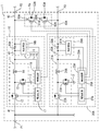
- FIG. 1 is a circuit diagram schematically illustrating a vehicle power supply system including the vehicle power supply device according to the first embodiment.
- FIG. 2 is a circuit diagram showing a part of the vehicle power supply device according to the first embodiment.
- FIG. 3 is a circuit diagram illustrating the power supply device for a vehicle according to the first embodiment, omitting portions different from the omitted portions in FIG.
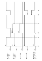
- FIG. 4 shows the state of the first power supply circuit, the state of the second power supply circuit, the state of the switch unit (first switch unit), the state of the second switch unit, and the second conductive path in the vehicle power supply device of the first embodiment. It is a timing chart which illustrates change with time about the voltage of.
- the second conductive path may be electrically connected to a second power storage unit different from the vehicle power storage unit.
- the vehicle power supply device of the present invention may include a detection unit that detects a value of a voltage applied to the second conductive path or a value of a current flowing through the second conductive path.
- the first power supply circuit converts a voltage applied to the first conductive path, generates a voltage to be applied to the second conductive path, and a value of the voltage applied to the second conductive path or the second
- a drive unit that drives the voltage conversion unit so that the value of the current flowing through the conductive path becomes a target value.
- the control unit may turn on the switch unit by setting a case where the voltage value or current value detected by the detection unit is lower than the target value by a certain value or more as a predetermined abnormal state.
- This vehicle power supply device operates to switch the switch unit to the ON state when the voltage or current of the second conductive path is lowered to a certain extent, and to supplement the power from the third conductive path side to the second conductive path side. Therefore, even if a situation occurs in which the voltage or current of the second conductive path is lowered to a certain degree, it is easy to suppress the voltage drop or current drop of the second conductive path.
- the vehicle power supply device of the present invention may include a plurality of second power supply circuits, third conductive paths, and switch portions.
- Each of the plurality of second power supply circuits may be connected to the plurality of third conductive paths.
- Each of the plurality of switch parts is provided between each of the plurality of third conductive paths and the second conductive path, and any switch part is connected from the corresponding third conductive path side to the second conductive path side. You may operate
- This vehicle power supply device can supply power to each second load by each second power supply circuit, and is less susceptible to voltage drop or current drop on the second conductive path side. Power supply can be performed stably.
- the plurality of switch units are switched to the on state, and power can be supplied from each third conductive path side to the second conductive path side.
- a predetermined abnormal state occurs on the second conductive path side
- a plurality of paths for supplementing electric power are secured, so that power supply from the third conductive path side to the second conductive path side is more reliable and sufficient. It is easy to be done.
- the vehicle power supply device of the present invention may include a diode that is provided in parallel to the switch unit, and whose anode is connected to the second conductive path side and whose cathode is connected to the third conductive path side. And when the control part is maintaining the switch part in an OFF state, the anode of a diode and the 2nd conductive path may be connected, and the cathode and the 3rd conductive path may be connected.
- the above-described vehicle power supply device in which the diode is provided in parallel with the switch unit may include a second switch unit connected in series with the switch unit between the second conductive path and the third conductive path.
- the second switch unit may be configured to switch between an off state in which power supply from the second conductive path side to the third conductive path side is interrupted and an on state that is allowed.
- the control unit turns off the switch unit and turns on the second switch unit when at least one of the first power supply circuit and the second conductive path is in a predetermined normal state, and a predetermined abnormal state.
- the switch unit may be turned on, and the second switch unit may be turned off when the second abnormal state is different from the predetermined normal state and the predetermined abnormal state.
- the switch portion When the vehicle power supply device is in a predetermined normal state, the switch portion is turned off and the second switch portion is turned on. Therefore, in the normal state, power from the third conductive path side to the second conductive path side is obtained. The supply is cut off, and the power supply from the second conductive path side to the third conductive path side is enabled via the diode provided in parallel with the switch section and the second switch section in the on state. Therefore, in the normal state, the influence of the voltage drop on the second conductive path side is less likely to reach the third conductive path side, and when the voltage drops on the third conductive path side, power is supplemented from the second conductive path side. Become.
- the switch unit When a predetermined abnormal state occurs, the switch unit is turned on, so that power supply from the third conductive path side to the second conductive path side is allowed. Therefore, electric power can be supplemented from the third conductive path side to the second conductive path side in a predetermined abnormal state.
- the second switch unit When the second abnormal state occurs, the second switch unit is turned off, so that a current flows from the second conductive path side to the third conductive path side through a diode provided in parallel with the switch unit. Can be blocked.
- the control unit may turn off the second switch unit by setting the case where the value of the voltage applied to the second conductive path is equal to or higher than a predetermined voltage threshold as the second abnormal state.
- the second switch unit is turned off when the voltage applied to the second conductive path is equal to or higher than a predetermined voltage threshold, and the current caused by the overvoltage is on the second conductive path side. From flowing to the third conductive path side can be blocked. Therefore, it is possible to prevent the influence of the overvoltage from reaching the third conductive path when the second conductive path is in the overvoltage state.
- Embodiment 1 of the present invention will be described below.
- 1 includes a first power storage unit 91 configured as a vehicle power storage unit and a second power storage unit 92 different from the first power storage unit 91.
- the vehicle power supply device 1 (hereinafter also simply referred to as the power supply device 1) and the wiring portions 71, 72, 73A, 73N are used to supply power to the first load 81 and the second loads 82A, 82N mounted on the vehicle. It is configured as a system that can supply.
- the first power storage unit 91 corresponds to an example of a vehicle power storage unit, and is configured by power storage means such as a lithium ion battery or an electric double layer capacitor to generate a first predetermined voltage.
- the potential of the high potential side terminal of the first power storage unit 91 is maintained at 48V, and the low potential side terminal is maintained at the ground potential (0V).
- the high potential side terminal of the first power storage unit 91 is electrically connected to the wiring unit 71 provided in the vehicle, and the first power storage unit 91 applies a predetermined voltage to the wiring unit 71.
- the low potential side terminal of the first power storage unit 91 is electrically connected to a ground part in the vehicle.
- the wiring portion 71 is connected to the input side terminal P1 of the power supply device 1 and is electrically connected to the first conductive path 41 via the input side terminal P1.
- 2nd electrical storage part 92 is comprised by electrical storage means, such as a lead storage battery, for example, and produces
- the high potential side terminal of the second power storage unit 92 is kept at 12V, and the low potential side terminal is kept at the ground potential (0V).
- the high potential side terminal of the second power storage unit 92 is electrically connected to a wiring unit 72 provided in the vehicle, and the second power storage unit 92 applies a predetermined voltage to the wiring unit 72.
- the low potential side terminal of the second power storage unit 92 is electrically connected to a ground part in the vehicle.
- the wiring part 72 is connected to the output side terminal P2 of the power supply device 1 and is electrically connected to the second conductive path 42 via the output side terminal P2.
- the first load 81 is a load that is electrically connected to the wiring unit 72 and is a load that receives power supply from the power supply device 1 or the second power storage unit 92 via the wiring unit 72.
- As the first load 81 various known vehicle loads can be used.
- the second loads 82A and 82N are loads electrically connected to the other wiring portions 73A and 73N, not the wiring portion 72 connected to the second power storage unit 92, and are connected via these wiring portions 73A and 73N. It is a load that receives power supply.
- As the second loads 82A and 82N various known vehicle loads can be used.
- the second loads 82 ⁇ / b> A and 82 ⁇ / b> N are different types of loads from the first load 81.
- the wiring portion 73A connected to the second load 82A is electrically connected to a third conductive path 43A described later via the output side terminal P3, and the second load 82A is connected to the third power supply circuit 20A through the third power supply circuit 20A.
- Electric power can be supplied through the conductive path 43A and the wiring part 73A.
- the wiring section 73N connected to the second load 82N is electrically connected to a third conductive path 43N, which will be described later, via the output side terminal P4, and the second load 82N is connected to the third power supply circuit 20N through the third power supply circuit 20N. Electric power can be supplied through the conductive path 43N and the wiring part 73N.
- the power supply device 1 includes a first conductive path 41, a second conductive path 42, a plurality of third conductive paths 43A and 43N, a reference conductive path 3, a first power supply circuit 10, and a plurality of second power supply circuits 20A. , 20N and a plurality of relay units Ra, Rn.
- the first conductive path 41 is a path through which power is supplied from the first power storage unit 91 (vehicle power storage unit), and is configured as a primary (high voltage side) power line to which a relatively high voltage is applied. Yes.
- the first conductive path 41 is electrically connected to the high potential side terminal of the first power storage unit 91 via the wiring unit 71, and a predetermined DC voltage is applied from the first power storage unit 91.
- an input side terminal P1 is provided at the end of the first conductive path 41, and a wiring portion 71 is connected to the input side terminal P1.
- the second conductive path 42 is configured as a secondary (low voltage side) power supply line to which a relatively low voltage is applied, and is a path electrically connected to one or more first loads 81.
- the second conductive path 42 is electrically connected to the high potential side terminal of the second power storage unit 92 via the wiring unit 72, and a DC voltage smaller than the output voltage of the first power storage unit 91 is applied from the second power storage unit 92.
- the structure is made.
- an output side terminal P2 is provided at an end of the second conductive path 42, and a wiring portion 72 is electrically connected to the output side terminal P2.
- the third conductive paths 43A and 43 are paths that are electrically connected to one or more second loads 82A and 82N different from the first load 81.
- the third conductive path 43A is electrically connected to the second load 82A via the wiring portion 73A.
- the third conductive path 43N is electrically connected to the second load 82N via the wiring portion 73N.
- the reference conductive path 3 is configured as a wiring pattern, a metal layer, or a metal member provided on a wiring board on which, for example, the first power supply circuit 10 and the second power supply circuits 20A and 20N are mounted. It is electrically connected to the part.
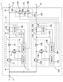
- FIG. 2 is a circuit diagram specifically showing the configuration of the power supply device 1, and some of the circuits (second power supply circuit 20N and the like) are omitted.
- the first power supply circuit 10 is configured as a step-down DCDC converter for a vehicle that is used by being mounted on a vehicle, and mainly includes a voltage conversion unit 11, a drive unit 15, a voltage detection unit 18, and a current detection unit. 19 and the like.
- the first power supply circuit 10 operates to step down the DC voltage (input voltage) applied to the first conductive path 41 and apply a desired DC voltage (output voltage) to the second conductive path 42.
- the voltage applied to the first conductive path 41 means a potential difference between the first conductive path 41 and the reference conductive path 3.
- the voltage applied to the second conductive path 42 means a potential difference between the second conductive path 42 and the reference conductive path 3.
- the voltage conversion unit 11 is provided between the first conductive path 41 and the second conductive path 42 and is configured as a high-side first element configured as a semiconductor switching element electrically connected to the first conductive path 41. 12, a semiconductor switching element electrically connected between the first element 12 and the reference conductive path 3 (conductive path maintained at a predetermined reference potential lower than the potential of the first conductive path 41). And the inductor 14 electrically connected between the first element 12 and the second element 13 and the second conductive path 42.
- the voltage conversion unit 11 is a main part of the switching-type step-down DCDC converter, and steps down the voltage applied to the first conductive path 41 by switching between the ON operation and the OFF operation of the first element 12 and performs the second conduction.
- the step-down operation output to the path 42 can be performed.
- Each of the first element 12 and the second element 13 is configured as an N-channel MOSFET, and one end of the first conductive path 41 is connected to the drain of the first element 12 on the high side. 41 and the wiring part 71 (FIG. 1) are also electrically connected to the high potential side terminal of the first power storage unit 91.
- the source of the first element 12 is electrically connected to the drain of the second element 13 on the low side and one end of the inductor 14.
- a driving signal and a non-driving signal from the driving circuit 17 provided in the driving unit 15 are input to the gate of the first element 12, and the first element 12 is output according to the signal from the driving unit 15. Is switched between an on state and an off state.
- the source of the second element 13 on the low side is electrically connected to the reference conductive path 3 and is kept at the ground potential.
- a drive signal and a non-drive signal from the drive unit 15 are also input to the gate of the second element 13, and the second element 13 is turned on and off according to the signal from the drive unit 15. It is supposed to switch to.
- One end of the inductor 14 is connected to a connection portion between the first element 12 and the second element 13, and one end thereof is electrically connected to the source of the first element 12 and the drain of the second element 13. The other end of the inductor 14 is electrically connected to the second conductive path 42.
- the voltage detector 18 is configured to be electrically connected to the second conductive path 42 and to input a value corresponding to the voltage at a predetermined position of the second conductive path 42 to the control circuit 16.
- the voltage detection unit 18 may be a known voltage detection circuit that can input a value indicating the voltage of the second conductive path 42 (the voltage at the connection position of the voltage detection unit 18) to the control circuit 16, as shown in FIG.
- the voltage value of the second conductive path 42 may be directly input to the control circuit 16, and the voltage is divided so that the voltage of the second conductive path 42 is divided and input to the control circuit 16. It may be configured as a circuit.
- the current detection unit 19 includes a resistor 19A and a detection circuit 19B, and indicates a value indicating the current flowing through the second conductive path 42 (specifically, an analog voltage corresponding to the value of the current flowing through the second conductive path 42). Is output.
- the detection circuit 19B is configured as, for example, a differential amplifier, and a voltage drop generated in the resistor 19A due to the output current from the voltage conversion unit 11 is amplified by the detection circuit 19B (differential amplifier) and detected according to the output current.
- a voltage (analog voltage) is input to the control circuit 16.
- the detected voltage (analog voltage) is converted into a digital value by an A / D converter (not shown) provided in the control circuit 16.
- the drive unit 15 includes a control circuit 16 and a drive circuit 17.
- the control circuit 16 is configured as a microcomputer, for example, a CPU that performs various arithmetic processes, a ROM that stores information such as programs, a RAM that stores temporarily generated information, and an analog voltage that is input into a digital value.
- An A / D converter for conversion is provided.
- the control circuit 16 detects the voltage of the second conductive path 42 (potential difference between the second conductive path 42 and the reference conductive path 3) by the voltage detection unit 18 when the voltage conversion unit 11 performs the step-down operation.
- a feedback calculation is performed so that the voltage of the second conductive path 42 approaches the set target value, and a PWM signal is generated. That is, if the voltage of the second conductive path 42 detected by the voltage detector 18 is smaller than the target value, the duty is increased by feedback calculation so as to approach the target value, and the second conductive path detected by the voltage detector 18. If the voltage of 42 is larger than the target value, the duty is adjusted so as to reduce the duty by feedback calculation so as to approach the target value.
- the drive circuit 17 Based on the PWM signal supplied from the control circuit 16, the drive circuit 17 generates an ON signal for alternately turning on each of the first element 12 and the second element 13 in each control cycle. Applied to the gate of the two elements 13.
- the ON signal applied to the gate of the first element 12 is given an ON signal whose phase is substantially inverted with respect to the ON signal applied to the gate of the second element 13 and so-called dead time is ensured.
- the second power supply circuit 20 ⁇ / b> A is also configured as a vehicle step-down DCDC converter similar to the first power supply circuit 10.
- the second power supply circuit 20A mainly includes a voltage conversion unit 21A, a control unit 25A, a voltage detection unit 28A, a current detection unit 29A, etc., and the basic configuration and basic operation are the same as those of the first power supply circuit 10. It operates so as to step down the DC voltage (input voltage) applied to the first conductive path 41 and apply a desired DC voltage (output voltage) to the third conductive path 43A.
- the voltage applied to the third conductive path 43A means a potential difference between the third conductive path 43A and the reference conductive path 3.
- the voltage conversion unit 21A is provided between the first conductive path 41 and the third conductive path 43A, and is a first element on the high side that is configured as a semiconductor switching element electrically connected to the first conductive path 41. 22A, the second element 23A on the low side configured as a semiconductor switching element electrically connected between the first element 22A and the reference conductive path 3, the first element 22A, the second element 23A, and the third And an inductor 24A electrically connected to the conductive path 43A. Both the first element 22A and the second element 23A are configured as N-channel MOSFETs.
- the voltage detector 18 is configured to be electrically connected to the third conductive path 43A and to input a value corresponding to the voltage at a predetermined position of the third conductive path 43A to the control circuit 26A.
- the voltage detection unit 28A is configured as a known voltage detection circuit that can input a value indicating the voltage of the third conductive path 43A (the voltage at the connection position of the voltage detection unit 28A) to the control circuit 26A.
- the current detection unit 29A includes a resistor 30A and a detection circuit 31A, and indicates a value indicating the current flowing through the third conductive path 43A (specifically, an analog voltage corresponding to the value of the current flowing through the third conductive path 43A). Is output.
- the detection circuit 31A is configured as a differential amplifier, for example, and a voltage drop generated in the resistor 30A due to the output current from the voltage conversion unit 21A is amplified by the detection circuit 31A (differential amplifier) and detected according to the output current. It becomes a voltage (analog voltage) and is input to the control circuit 26A.
- the control unit 25A includes a control circuit 26A and a drive circuit 27A.
- the control circuit 26A is configured as a microcomputer, for example, and includes a CPU, a ROM, a RAM, an A / D converter, and the like.
- the control circuit 26 detects the voltage of the third conductive path 43A (potential difference between the third conductive path 43A and the reference conductive path 3) by the voltage detection unit 28A.
- a feedback calculation is performed so that the voltage of the third conductive path 43A approaches the set target value, and a PWM signal is generated.
- the drive circuit 27A generates an ON signal for alternately turning on each of the first element 22A and the second element 23A in each control cycle based on the PWM signal given from the control circuit 26A. Applied to the gate of the two elements 23A.
- the power supply device 1 is provided with a circuit having the same configuration as the second power supply circuit 20A described above in parallel with the second power supply circuit 20A.
- the second power supply circuit 20N is also configured as a vehicle step-down DCDC converter similar to the first power supply circuit 10 and the second power supply circuit 20A.
- FIG. 3 is a circuit diagram specifically showing the configuration of the power supply device 1, and some of the circuits (the second power supply circuit 20A, etc.) are omitted.
- the second power supply circuit 20N mainly includes a voltage conversion unit 21N, a control unit 25N, a voltage detection unit 28N, a current detection unit 29N, and the like, and the basic configuration and basic operation are the same as those of the first power supply circuit 10 and the second power supply circuit 20A.
- the DC voltage (input voltage) applied to the first conductive path 41 is stepped down, and a desired DC voltage (output voltage) is applied to the third conductive path 43N.
- the voltage applied to the third conductive path 43N means a potential difference between the third conductive path 43N and the reference conductive path 3.
- the voltage conversion unit 21N is provided between the first conductive path 41 and the third conductive path 43N, and is a first element on the high side configured as a semiconductor switching element electrically connected to the first conductive path 41. 22N, a low-side second element 23N configured as a semiconductor switching element electrically connected between the first element 22N and the reference conductive path 3, a first element 22N, a second element 23N, and a third element And an inductor 24N electrically connected to the conductive path 43N. Both the first element 22N and the second element 23N are configured as N-channel MOSFETs.
- the voltage detector 18 is configured to be electrically connected to the third conductive path 43N and to input a value corresponding to the voltage at a predetermined position of the third conductive path 43N to the control circuit 26N.
- the voltage detection unit 28N is configured as a known voltage detection circuit that can input a value indicating the voltage of the third conductive path 43N (the voltage at the connection position of the voltage detection unit 28N) to the control circuit 26N.
- the current detection unit 29N includes a resistor 30N and a detection circuit 31N, and indicates a value indicating the current flowing through the third conductive path 43N (specifically, an analog voltage corresponding to the value of the current flowing through the third conductive path 43N). Is output.
- the detection circuit 31N is configured as, for example, a differential amplifier, and a voltage drop generated in the resistor 30N due to the output current from the voltage conversion unit 21N is amplified by the detection circuit 31N (differential amplifier) and detected according to the output current. It becomes a voltage (analog voltage) and is input to the control circuit 26N.
- the control unit 25N includes a control circuit 26N and a drive circuit 27N.
- the control circuit 26N is configured as a microcomputer, for example, and includes a CPU, a ROM, a RAM, an A / D converter, and the like.
- the control circuit 26 detects the voltage of the third conductive path 43N (potential difference between the third conductive path 43N and the reference conductive path 3) by the voltage detection unit 28N.
- a feedback calculation is performed so that the voltage of the third conductive path 43N approaches the set target value, and a PWM signal is generated.
- the drive circuit 27N generates an ON signal for alternately turning on each of the first element 22N and the second element 23N in each control cycle based on the PWM signal supplied from the control circuit 26N, and the first element 22N and the second element 23N. Applied to the gate of the two elements 23N.
- the power supply device 1 is provided with the plurality of second power supply circuits 20A and 20N in parallel, both of which function as a synchronous rectification step-down DCDC converter, and the voltage applied to the first conductive path 41. And a desired voltage is applied to the corresponding third conductive path.
- the second power supply circuit 20A is applied to the first conductive path 41 by performing switching between the ON operation and the OFF operation of the second element 23A on the low side in synchronization with the operation of the first element 22A on the high side.
- the DC voltage (input voltage) thus applied is stepped down, and a desired DC voltage (output voltage) is applied to the third conductive path 43A.
- the second power supply circuit 20N performs switching between the ON operation and the OFF operation of the low-side second element 23N in synchronization with the operation of the high-side first element 22N.
- the direct current voltage (input voltage) applied to 41 is stepped down, and a desired direct current voltage (output voltage) is applied to the third conductive path 43N.
- the first power supply circuit 10 is connected to the second conductive path 42, and each of the plurality of second power supply circuits 20A and 20N includes a plurality of third conductive paths 43A and 43N. Are connected to each.
- Relay paths Ra and Rn are provided in each path between the plurality of third conductive paths 43A and 43N and the second conductive path 42, and switch sections 51A and 51N are respectively provided in the paths. Intervene.
- the relay unit Ra includes a MOSFET 50A that partially functions as the switch unit 51A and a MOSFET 60A that partially functions as the second switch unit 62A.
- the MOSFET 50A and the MOSFET 60A include the second conductive path 42 and the third conductive path 43A. Are connected in series.
- the MOSFET 50A is configured as an N-channel type MOSFET, the source is electrically connected to the second conductive path 42, and the drain is electrically connected to the drain of the MOSFET 60A.
- the diode 53A is a body diode of the MOSFET 50A, the anode is electrically connected to the second conductive path 42, and the cathode is electrically connected to the drain of the MOSFET 60A and the cathode of the diode 63A.
- the portion excluding diode 53A is switch unit 51A.
- the switch unit 51A is provided between the third conductive path 43A and the second conductive path 42, and is in an off state in which the power supply from the third conductive path 43A side to the second conductive path 42 side is cut off and allowed on. Switch to state.
- the MOSFET 60A is configured as an N-channel type MOSFET, the source is electrically connected to the third conductive path 43A, and the drain is electrically connected to the drain of the MOSFET 50A.
- the diode 63A is a body diode of the MOSFET 60A, and has an anode electrically connected to the third conductive path 43A and a cathode electrically connected to the drain of the MOSFET 50A and the cathode of the diode 53A.
- the portion excluding the diode 63A is the second switch portion 62A.
- the second switch part 62A is connected in series with the switch part 51A between the second conductive path 42 and the third conductive path 43A, and cuts off the power supply from the second conductive path 42 side to the third conductive path 43A side. Switching between an off state to be performed and an on state to be permitted.
- the relay unit Rn has the same configuration as the relay unit Ra and functions in the same manner as the relay unit Ra.
- the relay unit Rn includes a MOSFET 50N that partially functions as the switch unit 51N and a MOSFET 60N that partially functions as the second switch unit 62N.
- the MOSFET 50N and the MOSFET 60N include the second conductive path 42 and the third conductive path 43N. Are connected in series.
- a portion of the MOSFET 50N excluding the diode 53N (body diode) is the switch portion 51N.
- the portion excluding the diode 63N is the second switch unit 62N.
- an on signal for example, an ignition on signal
- an off signal for example, an ignition off signal
- the signal input to the power supply device 1 is switched from an off signal (a signal indicating that the start switch is in an off state) to an on signal (a signal indicating that the start switch is in an on state).
- the timing is time t1.
- the drive unit 15 of the first power supply circuit 10 starts driving the voltage conversion unit 11 on the condition that the signal applied to the power supply device 1 from the outside is switched from the off signal to the on signal. Perform voltage conversion operation.
- the first power supply circuit 10 functions as a synchronous rectification step-down DCDC converter, and is controlled between the ON operation and the OFF operation of the second element 13 on the low side by the control of the drive unit 15.
- the DC voltage (input voltage) applied to the first conductive path 41 is stepped down, and a desired DC voltage (output voltage) is applied to the second conductive path 42.
- the magnitude of the DC voltage (output voltage) applied to the second conductive path 42 is determined according to the duty ratio of the PWM signal applied to the gate of the first element 12.
- target values for the target voltage and the target current are input to the drive unit 15 from an external ECU 102 (control ECU) provided outside the power supply device 1.
- the drive unit 15 The voltage conversion unit 11 is caused to perform a step-down operation while adjusting the duty of the PWM signal by repeating the feedback calculation so that the voltage value and the current value are close to the target voltage value and the target current value instructed from the external ECU 102.
- Various known controls can be employed.
- the drive unit 15 restricts one or both of the target voltage value and the target current value to be smaller than the value instructed from the external ECU 102 when the predetermined condition is satisfied.
- the voltage value of either the first conductive path 41 or the second conductive path 42 may be a predetermined voltage value or more, and the first conductive path 41 or the second conductive path may be satisfied.
- the current value of any of the paths 42 may be a predetermined current value or more, or the temperature at a predetermined position of the power supply device 1 may be a predetermined temperature or more.
- one or both of the target voltage value and the target current value are limited to be smaller than the value instructed from the external ECU 102.
- the drive unit 15 sets the target voltage value and the target current value to values instructed by the external ECU 102 (control ECU) in the normal state, and when the predetermined condition is satisfied, either of the target voltage value or the target current value is set. One or both of them is limited to be smaller than the value instructed from the external ECU 102.
- the target voltage value and the target current value are set, and the voltage value (actual voltage value) and current of the second conductive path 42 detected by the voltage detection unit 18, the current detection unit 19, and the control circuit 16. Based on the value (actual current value), the drive unit 15 controls the voltage value and current value of the second conductive path 42 to approach the target voltage value and the target current value.
- control units 25A and 25N of the second power supply circuits 20A and 20N also have the voltage conversion units 21A and 21N as starting conditions when the signal supplied to the power supply device 1 from the outside is switched from the off signal to the on signal. Driving is started and voltage conversion operation is performed.
- Each of the second power supply circuits 20A and 20N also functions as a synchronous rectification step-down DCDC converter.
- the second power supply circuit 20A shown in FIG. 2 steps down the DC voltage (input voltage) applied to the first conductive path 41 under the control of the control unit 25A, and applies a desired DC voltage (output voltage) to the third conductive path 43A. ) Is applied.
- the magnitude of the DC voltage (output voltage) applied to the third conductive path 43A is determined according to the duty ratio of the PWM signal applied to the gate of the first element 22A.
- the second power supply circuit 20N shown in FIG. 3 steps down the DC voltage (input voltage) applied to the first conductive path 41 under the control of the control unit 25N, and applies a desired DC voltage (output voltage) to the third conductive path 43N. ) Is applied.
- the magnitude of the DC voltage (output voltage) applied to the third conductive path 43N is determined according to the duty ratio of the PWM signal applied to the gate of the first element 22N.
- the control circuit 16 of the drive unit 15 shown in FIG. 2 has a predetermined first difference between the voltage value (actual voltage value) of the second conductive path 42 detected by the voltage detection unit 18 and the target voltage value being set.
- a predetermined normal signal is output to the control circuit 26A of the second power supply circuit 20A and the control circuit 26N of the second power supply circuit 20N.
- the voltage value (actual voltage value) of the second conductive path 42 detected by the voltage detection unit 18 is lower than the target voltage value being set, and the difference between them is not less than the first value. In some cases, or the current value (actual current value) of the second conductive path 42 detected by the current detector 19 is lower than the target current value being set, and the difference between them is equal to or greater than the second value.
- the first abnormality signal is output to the control circuit 26A of the second power supply circuit 20A and the control circuit 26N of the second power supply circuit 20N. In the example of FIG. 4, for some reason, the output of the first power supply circuit 10 is stopped at time t2, and the first abnormal signal is output at time t3.
- control circuit 16 is configured such that the voltage value (actual voltage value) of the second conductive path 42 detected by the voltage detection unit 18 is equal to or higher than a predetermined voltage threshold value (in a second abnormal state), A second abnormality signal is output to the control circuit 26A of the second power supply circuit 20A and the control circuit 26N of the second power supply circuit 20N.
- the control unit 25A of the second power supply circuit 20A receives a normal signal from the control circuit 16 after the drive of the voltage conversion unit 21A is started (that is, the first power supply circuit 10 and the second conductive path 42 have a predetermined normality).
- the switch unit 51A first switch unit
- the second switch unit 62A is turned on.
- the third conductive path 43A side Current is prevented from flowing to the second conductive path 42 side.
- the control unit 25N of the second power supply circuit 20N operates in the same manner, and when the normal signal is output from the control circuit 16 after the drive of the voltage conversion unit 21N is started, the switch unit 51N (first switch unit) is turned off. And the second switch 62N is turned on to block the current from flowing from the third conductive path 43N to the second conductive path 42 while the potential of the third conductive path 43N is set to the second conductive path 42.
- a current flows through the diode 53N and the second switch portion 62N.
- the control unit 25A of the second power supply circuit 20A that is, the second conductive path 42 detected by the detection unit 5.
- the switch unit 51A first 1 switch part
- the control unit 25N of the second power supply circuit 20N switches the switch unit 51N (first switch unit) when the first abnormality signal is output from the control circuit 16 after the drive of the voltage conversion unit 21N is started.
- the second switch unit 62N is also kept on in the on state. As described above, when the output to the second conductive path 42 is lowered, the switch units 51A and 51N are switched to the on state, so that part of the power supplied from the second power supply circuits 20A and 20N is part of the second conductive path. 42 will be replenished.
- the first abnormal signal is output from the control circuit 16 during the period from time t3 to time t4. In addition, after the time t4, the first abnormal signal is canceled, and a normal signal is output from the time t4 to the time t5.
- the control unit 25A of the second power supply circuit 20A detects the second conductive path 42 detected by the detection unit 5.
- the switch unit 51A first switch unit
- the second switch unit 62A is also turned off.
- the control unit 25N of the second power supply circuit 20N switches the switch unit 51N (first switch unit) when the second abnormality signal is output from the control circuit 16 after the drive of the voltage conversion unit 21N is started. The off state is set, and the second switch unit 62N is also turned off.
- the second switch portions 62A and 62N are switched to the off state, so that the influence of the overvoltage of the second conductive path 42 is applied to the third conductive paths 43A and 43N.
- the second abnormal signal is output from the control circuit 16 during the period from time t5 to time t6.
- the vehicle power supply device 1 described above converts a voltage applied to the first conductive path 41 that is a path to which power is supplied from the first power storage unit 91 (vehicle power storage unit), and converts the voltage to the second conductive path 42.
- a second power supply circuit 20A, 20N that converts a voltage applied to the first conductive path 41 and applies a voltage to the third conductive paths 43A, 43N. Since it is configured in this way, electric power can be supplied to the first load 81 via the second conductive path 42, and the third conductive path 43A, the second load 82A, 82N can be supplied. Power can be supplied through 43N.
- control units 25A and 25N turn on the switch units 51A and 51N when at least one of the first power supply circuit 10 and the second conductive path 42 is in a predetermined abnormal state, and otherwise the switch unit 51A. , 51N are turned off.
- the switch portions 51A and 51N are turned off, and the power supply from the third conductive paths 43A and 43N to the second conductive path 42 is interrupted. Even if a temporary voltage drop or the like occurs in the conductive path 42, current can be prevented from flowing from the third conductive path 43A, 43N side to the second conductive path 42 side.
- the state on the second conductive path 42 side hardly affects the third conductive paths 43A and 43N, and the state of the third conductive paths 43A and 43N is easily maintained stably.
- the switch portions 51A and 51N are turned on, and power supply from the third conductive paths 43A and 43N to the second conductive path 42 is allowed.
- the power is supplemented from the third conductive paths 43A and 43N side, and the decrease in voltage or current can be suppressed.
- the second conductive path 42 is electrically connected to a second power storage unit 92 different from the first power storage unit 91 (vehicle power storage unit).
- power can be supplied from the second power storage unit 92 to the first load 81, and the second power storage unit 92 can be charged by power supplied from the first power supply circuit 10.
- the charging voltage of the second power storage unit 92 decreases, the first load 81 is easily affected, but the second loads 82A and 82N electrically connected to the third conductive paths 43A and 43N are not affected. Is less affected by a decrease in charging voltage.
- the vehicle power supply device 1 includes a detection unit 5 that detects a value of a voltage applied to the second conductive path 42 or a value of a current flowing through the second conductive path 42.
- the voltage detection unit 18, the current detection unit 19, and the control circuit 16 constitute the detection unit 5.
- the first power supply circuit 10 converts the voltage applied to the first conductive path 41 and generates a voltage to be applied to the second conductive path 42, and is applied to the second conductive path 42.
- a drive unit 15 that drives the voltage conversion unit 11 so that the value of the voltage or the value of the current flowing through the second conductive path 42 becomes a target value.
- the control units 25A and 25N operate to turn on the switch units 51A and 51N with a predetermined abnormality state when the voltage value or current value detected by the detection unit 5 is lower than the target value by a certain value or more. .
- the vehicle power supply device 1 switches the switch portions 51A and 51N to the on state, and the second conductive path from the third conductive paths 43A and 43N side. It operates to supplement power on the 42 side. Therefore, even if the voltage value or current value of the second conductive path 42 decreases to a certain degree, it is easy to suppress the voltage drop or current decrease of the second conductive path 42.
- the vehicle power supply device 1 includes a plurality of second power supply circuits 20A and 20N, a plurality of third conductive paths 43A and 43N, and a plurality of switch units 51A and 51N.
- Each of the plurality of second power supply circuits 20A and 20N is connected to the plurality of third conductive paths 43A and 43N, respectively, and each of the plurality of switch portions 51A and 51N is connected to the plurality of third conductive paths 43A and 43N.
- the second conductive path 42 are provided. Then, both of the switch parts 51A and 51N operate so as to be switched between an off state in which power supply from the corresponding third conductive path side to the second conductive path 42 side is cut off and an allowed on state.
- the vehicular power supply device 1 can supply power to each of the second loads 82A and 82N by the second power supply circuits 20A and 20N, respectively, and has the effect of voltage drop or current drop on the second conductive path 42 side. In a form that is difficult to receive, power supply to the second loads 82A and 82N is easily performed stably.
- the plurality of switch units 51A and 51N are switched to the on state, and power can be supplied from the third conductive paths 43A and 43N to the second conductive path 42 side. Become.
- the vehicle power supply device 1 includes diodes 53A and 53N which are provided in parallel to the switch unit, and whose anode is connected to the second conductive path 42 side and whose cathode is connected to the third conductive path side.
- the control units 25A and 25N maintain the switch units 51A and 51N in the OFF state
- the anodes of the diodes 53A and 53N are electrically connected to the second conductive path 42, and the respective cathodes are connected to the third conductive path 43A, It is configured to be electrically connected to each of 43N.
- the vehicle power supply device 1 tries to flow from the third conductive path 43A, 43N side to the second conductive path 42 side when the control units 25A, 25N maintain the switch units 51A, 51N in the OFF state.
- the current is interrupted, the currents that try to flow from the second conductive path 42 side to the third conductive paths 43A and 43N are allowed by the diodes 53A and 53N. That is, even if the voltage applied to the third conductive paths 43A and 43N is greatly reduced with respect to the voltage applied to the second conductive path 42, the third conductive paths from the second conductive path 42 through the diodes 53A and 53N.
- the third conductive paths 43A and 43N which are paths for supplying power to the second loads 82A and 82N, can be more easily stabilized.
- the vehicle power supply device 1 is provided with second switch parts 62A and 62N in series with each of the switch parts 51A and 51N between the second conductive path 42 and the third conductive paths 43A and 43N, respectively.
- 2nd switch part 62A, 62N becomes a structure switched to the OFF state which interrupts
- the control units 25A and 25N turn off the switch units 51A and 51N and turn on the second switch units 62A and 62N when the first power supply circuit 10 and the second conductive path 42 are in a predetermined normal state.
- the switch units 51A and 51N are turned on when a predetermined abnormal state is detected, and the second switch units 62A and 62N are turned off when the second abnormal state is different from the predetermined normal state and the predetermined abnormal state. Operates to state.
- the switch portions 51A and 51N are turned off and the second switch portions 62A and 62N are turned on.
- the power supply from the second conductive path 42 side to the second conductive path 42 side is cut off, and the power supply from the second conductive path 42 side to the third conductive paths 43A, 43N side is a diode provided in parallel with the switch parts 51A, 51N This is possible through 53A, 53N and the second switch portions 62A, 62N that are turned on. Therefore, in the normal state, the influence of the voltage drop on the second conductive path 42 side hardly reaches the third conductive paths 43A and 43N side, and when the voltage drops on the third conductive path 43A and 43N side, The electric power is supplemented from the two conductive paths 42 side.
- the switch portions 51A and 51N are turned on, so that power supply from the third conductive path 43A and 43N side to the second conductive path 42 side is allowed. Therefore, in a predetermined abnormal state, power can be supplemented from the third conductive path 43A, 43N side to the second conductive path 42 side.
- the second switch parts 62A and 62N are turned off, so that the second conductive path 42 side is provided via the diodes 53A and 53N provided in parallel with the switch parts 51A and 51N.
- the control units 25A and 25N turn off the second switch units 62A and 62N by setting the case where the value of the voltage applied to the second conductive path 42 is equal to or greater than a predetermined voltage threshold as the second abnormal state.
- the vehicular power supply device 1 turns off the second switch portions 62A and 62N when the voltage applied to the second conductive path 42 is equal to or higher than a predetermined voltage threshold, and the current caused by the overvoltage. Can be prevented from flowing from the second conductive path 42 side to the third conductive paths 43A, 43N side. Therefore, it is possible to prevent the influence of the overvoltage from reaching the third conductive paths 43A and 43N when the second conductive path 42 is in the overvoltage state.
- the configuration in which the two second power supply circuits 20A and 20N are provided is illustrated.
- the number of the second power supply circuits may be one, or may be three or more.
- the first power supply circuit 10 and the second power supply circuits 20A and 20N are step-down DCDC converters, but may be step-up DCDC converters. Alternatively, it may operate as a step-up / step-down DCDC converter.
- the configuration in which the abnormal signal is output from the control circuit 16 of the first power supply circuit 10 is exemplified.
- the control units 25A and 25N (specifically, the control circuits 26A of the second power supply circuits 20A and 20N). , 26N) can acquire information (specifically, information on the target voltage value and target current value being set, information on the voltage value and current value detected by the detection unit 5) from the control circuit 16. It may be configured.
- the difference between the voltage value (actual voltage value) of the second conductive path 42 and the target voltage value is less than the predetermined first value, and the second conductive path 42
- the above operation operation when a normal signal is output
- the above operation is performed as a normal state. Also good.
- the above-described operation (the first abnormal signal is output) is set as a predetermined abnormal state. May be performed).
- the above-described operation when the voltage value (actual voltage value) of the second conductive path 42 is equal to or higher than a predetermined voltage threshold, the above-described operation (second Operation when an abnormal signal is output) may be performed.
- both the first power supply circuit 10 and the second power supply circuits 20A, 20N are single-phase DCDC converters, but any or all of them may be multiphase DCDC converters.
- the configuration in which the second power storage unit 92 is electrically connected to the second conductive path 42 on the output side is illustrated, but the second power storage unit 92 is electrically connected to the second conductive path 42. It does not have to be.
- each of the first power supply circuit 10 and the second power supply circuits 20A and 20N is a synchronous rectification step-down DCDC converter in which the second element is configured as a switching element. It may be a diode-type step-down DCDC converter configured as a diode (a diode having a cathode connected to the first element side and an anode connected to the reference conductive path side).
Abstract
第1負荷に対する電力供給の影響を抑えた形で第2負荷に対して安定的に電力を供給し、所定の異常状態が発生した場合には、第2負荷に対応する電力供給経路側から第1負荷に対応する電力供給経路側へと電力を補充する。 車両用電源装置(1)は、第1導電路(41)に印加された電圧を変換して第2導電路(42)に電圧を印加する第1電源回路(10)と、第1導電路(41)に印加された電圧を変換して第3導電路(43A,43N)に電圧を印加する第2電源回路(20A,20N)とを備え、第3導電路(43A,43N)と第2導電路(42)との間にはスイッチ部(51A,51N)が設けられる。制御部(25A,25N)は、第1電源回路(10)又は第2導電路(42)の少なくともいずれかが所定の異常状態でない場合にスイッチ部(51A,51N)をオフ状態とし、所定の異常状態である場合にスイッチ部(51A,51N)をオン状態とする。
Description
本発明は、車両用電源装置に関するものである。
特許文献1には、車両用蓄電部(高電圧バッテリ)及びオルタネータから供給される高電圧を降圧し、低電圧系負荷及び第2蓄電部(低電圧バッテリ)に電力を供給し得る降圧回路を備えた車載用電源装置(電力供給回路)が開示されている。この電力供給回路では、通常のエンジン作動中に降圧回路が動作し、オルタネータから出力される高電圧が降圧回路により低電圧に降圧され、低電圧系負荷に電力が供給されるとともに、その余剰電力が第2蓄電部(低電圧バッテリ)に蓄えられる。
ところで、特許文献1で開示される車両用電源装置(車両の電力供給回路)は、全ての低電圧系負荷が降圧回路及び低電圧バッテリに電気的に接続された形で設けられているため、この経路で何らかの理由によって電圧低下が生じると、全ての低電圧系負荷に対する供給電圧が低下してしまうという問題がある。車両に搭載される負荷は、供給電圧が一時的に大きく変動しても許容される負荷もあれば、供給電圧をできるだけ変動させないことが望まれる負荷もある。供給電圧の安定性がより重要視される負荷に対しては、安定性及び独立性の高い供給経路を確保することが求められる。
本発明は、上述した事情に基づいてなされたものであり、第1負荷に対する電力供給の影響を抑えた形で第2負荷に対して安定的に電力を供給することができ、所定の異常状態が発生した場合には、第2負荷に対応する電力供給経路側から第1負荷に対応する電力供給経路側へと電力を補充し得る(第3導電路側から第2導電路側へと電力を供給し得る)車両用電源装置を実現することを目的とするものである。
本発明の一つの解決手段である車両用電源装置は、
車両用蓄電部から電力が供給される経路である第1導電路と、
1以上の第1負荷に電気的に接続される経路である第2導電路と、
前記第1負荷とは異なる1以上の第2負荷に電気的に接続される経路である1以上の第3導電路と、
前記第1導電路に印加された電圧を変換して前記第2導電路に電圧を印加する第1電源回路と、
前記第1導電路に印加された電圧を変換して前記第3導電路に電圧を印加する1以上の第2電源回路と、
前記第3導電路と前記第2導電路との間に設けられ、前記第3導電路側から前記第2導電路側への電力供給を遮断するオフ状態と、許容するオン状態とに切り替わる少なくとも1つのスイッチ部と、
前記第1電源回路又は前記第2導電路の少なくともいずれかが所定の異常状態でない場合に前記スイッチ部をオフ状態とし、前記所定の異常状態である場合に前記スイッチ部をオン状態とする制御部と、
を有する。
上記車両用電源装置は、車両用蓄電部から電力が供給される経路である第1導電路に印加された電圧を変換して第2導電路に電圧を印加する第1電源回路と、第1導電路に印加された電圧を変換して第3導電路に電圧を印加する1以上の第2電源回路と、を有する。このように構成されるため、第1負荷に対しては、第2導電路を介して電力を供給することができ、第2負荷に対しては、第3導電路を介して電力を供給することができる。
そして、制御部は、第1電源回路又は前記第2導電路の少なくともいずれかが所定の異常状態でない場合に前記スイッチ部をオフ状態とし、所定の異常状態である場合にスイッチ部をオン状態とするように動作する。このように、所定の異常状態でない場合には、スイッチ部がオフ状態となり、第3導電路側から第2導電路側への電力供給が遮断されるため、第2導電路で一時的な電圧低下などが生じても、第3導電路側から第2導電路側へ電流が流れ込むことを防止し得る。よって、所定の異常状態でない場合には、第2導電路側の状態が第3導電路に影響を与えにくくなり、第3導電路の状態が安定的に維持されやすくなる。
一方、所定の異常状態となった場合には、スイッチ部がオン状態となり、第3導電路側から第2導電路側への電力供給が許容される。このように動作する期間は、第2導電路側で電圧又は電流が低下しても、第3導電路側から電力が補われ、電圧又は電流の低下を抑制することができる。
ここで、本発明の望ましい例を示す。
本発明の車両用電源装置において、第2導電路は、車両用蓄電部とは異なる第2蓄電部に電気的に接続されていてもよい。
このようにすれば、第2蓄電部から第1負荷に電力が供給され得る構成、且つ、第1電源回路から供給される電力によって第2蓄電部が充電され得る構成となる。この構成では、第2蓄電部の充電電圧が低下した場合、第1負荷はその影響を受けやすいが、第3導電路に電気的に接続された第2負荷には、充電電圧の低下の影響が及びにくくなる。
本発明の車両用電源装置は、第2導電路に印加される電圧の値又は第2導電路を流れる電流の値を検出する検出部を有していてもよい。第1電源回路は、第1導電路に印加された電圧を変換し、第2導電路に印加する電圧を生成する電圧変換部と、第2導電路に印加される電圧の値又は前記第2導電路を流れる電流の値が目標値となるように電圧変換部を駆動する駆動部と、を備えていてもよい。制御部は、検出部が検出する電圧の値又は電流の値が目標値よりも一定値以上低い場合を所定の異常状態としてスイッチ部をオン状態としてもよい。
この車両用電源装置は、第2導電路の電圧又は電流が一定程度低下した場合にスイッチ部をオン状態に切り替え、第3導電路側から第2導電路側に電力を補うように動作する。よって、第2導電路の電圧又は電流が一定程度低下するような事態が生じても、第2導電路の電圧低下又は電流低下を抑えやすくなる。
本発明の車両用電源装置は、第2電源回路、第3導電路、及びスイッチ部がそれぞれ複数設けられていてもよい。そして、複数の第2電源回路の各々が、複数の第3導電路にそれぞれ接続されていてもよい。そして、複数のスイッチ部の各々が、複数の第3導電路の各々と第2導電路との間にそれぞれ設けられ、いずれのスイッチ部も、対応する第3導電路側から第2導電路側への電力供給を遮断するオフ状態と、許容するオン状態とに切り替わるように動作してもよい。
この車両用電源装置は、各第2電源回路によって各第2負荷に電力を供給することができ、第2導電路側の電圧低下又は電流低下の影響を受けにくい形で、各第2負荷への電力供給が安定的に行われやすくなる。一方、所定の異常状態が発生した場合には、複数のスイッチ部がオン状態に切り替えられ、各第3導電路側から第2導電路側へ電力が供給され得る状態となる。このように、第2導電路側で所定の異常状態が発生したとき、電力を補うための経路が複数確保されるため、第3導電路側から第2導電路側への電力供給がより確実且つより十分に行われやすくなる。
本発明の車両用電源装置は、スイッチ部に対して並列に設けられるとともに、アノードが第2導電路側に接続され、カソードが第3導電路側に接続されるダイオードを有していてもよい。そして、制御部がスイッチ部をオフ状態で維持しているときに、ダイオードのアノードと第2導電路とが導通し、カソードと第3導電路とが導通する構成であってもよい。
この車両用電源装置は、制御部がスイッチ部をオフ状態で維持しているとき、第3導電路側から第2導電路側へ流れ込もうとする電流は遮断されるが、第2導電路側から第3導電路側へ流れ込もうとする電流はダイオードによって許容される。つまり、第3導電路に印加される電圧が第2導電路に印加される電圧に対して大きく低下しても、第2導電路からダイオードを介して第3導電路へ電流が流れ込むことで、第3導電路の電圧の低下が抑えられる。よって、第2負荷へ電力を供給するための経路である第3導電路を、より安定させやすくなる。
スイッチ部と並列にダイオードが設けられる上述の車両用電源装置は、第2導電路と第3導電路との間においてスイッチ部と直列に接続される第2スイッチ部を有していてもよい。そして、第2スイッチ部は、第2導電路側から第3導電路側への電力供給を遮断するオフ状態と、許容するオン状態とに切り替わる構成であってもよい。そして、制御部は、第1電源回路又は第2導電路の少なくともいずれかが、所定の正常状態である場合にスイッチ部をオフ状態とするとともに第2スイッチ部をオン状態とし、所定の異常状態である場合にスイッチ部をオン状態とし、所定の正常状態及び所定の異常状態とは異なる第2の異常状態である場合に第2スイッチ部をオフ状態とするように動作してもよい。
この車両用電源装置は、所定の正常状態である場合、スイッチ部がオフ状態となり、第2スイッチ部がオン状態となるため、正常状態のときには、第3導電路側から第2導電路側への電力供給は遮断され、第2導電路側から第3導電路側の電力供給は、スイッチ部と並列に設けられたダイオード及びオン状態とされた第2スイッチ部を介して可能となる。よって、正常状態のときには、第2導電路側での電圧低下の影響が第3導電路側に及びにくくなり、第3導電路側で電圧が低下した場合には第2導電路側から電力が補われるようになる。
所定の異常状態が発生した場合、スイッチ部がオン状態となるため、第3導電路側から第2導電路側への電力供給が許容される。よって、所定の異常状態のときには、第3導電路側から第2導電路側へ電力を補うことができる。
第2の異常状態が発生した場合、第2スイッチ部がオフ状態となるため、スイッチ部と並列に設けられたダイオードを介して第2導電路側から第3導電路側へ電流が流れ込むような状態を遮断することができる。
所定の異常状態が発生した場合、スイッチ部がオン状態となるため、第3導電路側から第2導電路側への電力供給が許容される。よって、所定の異常状態のときには、第3導電路側から第2導電路側へ電力を補うことができる。
第2の異常状態が発生した場合、第2スイッチ部がオフ状態となるため、スイッチ部と並列に設けられたダイオードを介して第2導電路側から第3導電路側へ電流が流れ込むような状態を遮断することができる。
制御部は、第2導電路に印加される電圧の値が所定の電圧閾値以上である場合を第2の異常状態として第2スイッチ部をオフ状態としてもよい。
この車両用電源装置は、第2導電路に印加される電圧が所定の電圧閾値以上となるような過電圧状態のときに第2スイッチ部をオフ状態とし、過電圧に起因する電流が第2導電路側から第3導電路側へ流れ込むことを遮断することができる。よって、第2導電路が過電圧状態のときに過電圧の影響が第3導電路に及ぶことを防ぐことができる。
<実施例1>
以下、本発明を具体化した実施例1について説明する。
図1で示す車両用電源システム100(以下、単に電源システム100ともいう)は、車両用蓄電部として構成される第1蓄電部91と、第1蓄電部91とは異なる第2蓄電部92と、車両用電源装置1(以下、単に電源装置1ともいう)と、配線部71,72,73A,73Nとを備え、車両に搭載された第1負荷81や第2負荷82A,82Nに電力を供給し得るシステムとして構成されている。
以下、本発明を具体化した実施例1について説明する。
図1で示す車両用電源システム100(以下、単に電源システム100ともいう)は、車両用蓄電部として構成される第1蓄電部91と、第1蓄電部91とは異なる第2蓄電部92と、車両用電源装置1(以下、単に電源装置1ともいう)と、配線部71,72,73A,73Nとを備え、車両に搭載された第1負荷81や第2負荷82A,82Nに電力を供給し得るシステムとして構成されている。
第1蓄電部91は、車両用蓄電部の一例に相当し、例えば、リチウムイオン電池、或いは電気二重層キャパシタ等の蓄電手段によって構成され、第1の所定電圧を発生させるものである。例えば、第1蓄電部91の高電位側端子の電位は48Vに保たれ、低電位側端子はグラウンド電位(0V)に保たれる。第1蓄電部91の高電位側端子は、車両内に設けられた配線部71に電気的に接続されており、第1蓄電部91は、配線部71に対して所定電圧を印加する。第1蓄電部91の低電位側端子は、車両内のグラウンド部に電気的に接続されている。配線部71は、電源装置1の入力側端子P1に接続されており、入力側端子P1を介して第1導電路41と導通している。
第2蓄電部92は、例えば、鉛蓄電池等の蓄電手段によって構成され、第1蓄電部91で発生する第1の所定電圧よりも低い第2の所定電圧を発生させるものである。例えば、第2蓄電部92の高電位側端子は12Vに保たれ、低電位側端子はグラウンド電位(0V)に保たれている。第2蓄電部92の高電位側端子は、車両内に設けられた配線部72に電気的に接続されており、第2蓄電部92は、配線部72に対して所定電圧を印加する。第2蓄電部92の低電位側端子は車両内のグラウンド部に電気的に接続されている。配線部72は、電源装置1の出力側端子P2に接続されており、出力側端子P2を介して第2導電路42と導通している。
第1負荷81は、配線部72に電気的に接続された負荷であり、配線部72を介して電源装置1又は第2蓄電部92から電力供給を受ける負荷である。第1負荷81としては、公知の様々な車両用負荷を用い得る。
第2負荷82A,82Nは、第2蓄電部92に接続された配線部72ではなく、他の配線部73A,73Nに電気的に接続された負荷であり、これら配線部73A,73Nを介して電力供給を受ける負荷である。第2負荷82A,82Nとしては、公知の様々な車両用負荷を用い得る。第2負荷82A,82Nは、第1負荷81と異なる種類の負荷となっている。第2負荷82Aに接続される配線部73Aは、出力側端子P3を介して後述する第3導電路43Aに電気的に接続されており、第2負荷82Aは、第2電源回路20Aから第3導電路43A及び配線部73Aを介して電力供給を受け得る。第2負荷82Nに接続される配線部73Nは、出力側端子P4を介して後述する第3導電路43Nに電気的に接続されており、第2負荷82Nは、第2電源回路20Nから第3導電路43N及び配線部73Nを介して電力供給を受け得る。
電源装置1は、第1導電路41と、第2導電路42と、複数の第3導電路43A,43Nと、基準導電路3と、第1電源回路10と、複数の第2電源回路20A,20Nと、複数のリレー部Ra,Rnとを備える。
第1導電路41は、第1蓄電部91(車両用蓄電部)から電力が供給される経路であり、相対的に高い電圧が印加される一次側(高圧側)の電源ラインとして構成されている。第1導電路41は、配線部71を介して第1蓄電部91の高電位側端子に導通するとともに、第1蓄電部91から所定の直流電圧が印加される構成をなす。図1の構成では、第1導電路41の端部に入力側端子P1が設けられ、この入力側端子P1に配線部71が接続されている。
第2導電路42は、相対的に低い電圧が印加される二次側(低圧側)の電源ラインとして構成され、1以上の第1負荷81に電気的に接続される経路である。第2導電路42は、配線部72を介して第2蓄電部92の高電位側端子に導通するとともに、第2蓄電部92から第1蓄電部91の出力電圧よりも小さい直流電圧が印加される構成をなす。図1の構成では、第2導電路42の端部に出力側端子P2が設けられ、この出力側端子P2に配線部72が電気的に接続されている。
第3導電路43A,43は、第1負荷81とは異なる1以上の第2負荷82A,82Nに電気的に接続される経路である。第3導電路43Aは、配線部73Aを介して第2負荷82Aに電気的に接続されている。第3導電路43Nは、配線部73Nを介して第2負荷82Nに電気的に接続されている。
基準導電路3は、例えば第1電源回路10、第2電源回路20A,20Nなどが実装される配線基板に設けられた配線パターン、金属層、或いは金属部材として構成されており、車両内のグラウンド部と電気的に接続されている。
図2は、電源装置1の構成を具体的に示す回路図であり、一部の回路(第2電源回路20Nなど)は省略して示している。図2のように、第1電源回路10は、車両に搭載されて使用される車両用降圧型DCDCコンバータとして構成され、主として、電圧変換部11、駆動部15、電圧検出部18、電流検出部19などを備える。第1電源回路10は、第1導電路41に印加された直流電圧(入力電圧)を降圧し、第2導電路42に所望の直流電圧(出力電圧)を印加するように動作する。第1導電路41に印加される電圧とは、第1導電路41と基準導電路3との電位差を意味する。第2導電路42に印加される電圧とは、第2導電路42と基準導電路3との電位差を意味する。
電圧変換部11は、第1導電路41と第2導電路42との間に設けられ、第1導電路41に電気的に接続された半導体スイッチング素子として構成されるハイサイド側の第1素子12と、第1素子12と基準導電路3(第1導電路41の電位よりも低い所定の基準電位に保たれる導電路)との間に電気的に接続された半導体スイッチング素子として構成されるローサイド側の第2素子13と、第1素子12及び第2素子13と第2導電路42との間に電気的に接続されたインダクタ14とを備える。電圧変換部11は、スイッチング方式の降圧型DCDCコンバータの要部をなし、第1素子12のオン動作とオフ動作との切り替えによって第1導電路41に印加された電圧を降圧して第2導電路42に出力する降圧動作を行い得る。
第1素子12及び第2素子13のいずれも、Nチャネル型のMOSFETとして構成され、ハイサイド側の第1素子12のドレインには、第1導電路41の一端が接続され、第1導電路41及び配線部71(図1)を介して第1蓄電部91の高電位側端子にも電気的に接続されている。第1素子12のソースには、ローサイド側の第2素子13のドレイン及びインダクタ14の一端が電気的に接続されている。第1素子12のゲートには、駆動部15に設けられた駆動回路17からの駆動信号及び非駆動信号が入力されるようになっており、駆動部15からの信号に応じて第1素子12がオン状態とオフ状態とに切り替わるようになっている。ローサイド側の第2素子13のソースは、基準導電路3に電気的に接続され、グラウンド電位に保たれるようになっている。第2素子13のゲートにも、駆動部15からの駆動信号及び非駆動信号が入力されるようになっており、駆動部15からの信号に応じて第2素子13がオン状態とオフ状態とに切り替わるようになっている。インダクタ14は、第1素子12と第2素子13との間の接続部に一端が接続され、その一端は第1素子12のソース及び第2素子13のドレインに電気的に接続されている。インダクタ14の他端は、第2導電路42に電気的に接続されている。
電圧検出部18は、第2導電路42に電気的に接続されるとともに第2導電路42の所定位置の電圧に応じた値を制御回路16に入力する構成をなす。電圧検出部18は、第2導電路42の電圧(当該電圧検出部18の接続位置の電圧)を示す値を制御回路16に入力し得る公知の電圧検出回路であればよく、図2のように、第2導電路42の電圧値を直接的に制御回路16に入力するように構成されていてもよく、第2導電路42の電圧を分圧して制御回路16に入力するような分圧回路として構成されていてもよい。
電流検出部19は、抵抗器19A及び検出回路19Bを有し、第2導電路42を流れる電流を示す値(具体的には、第2導電路42を流れる電流の値に応じたアナログ電圧)を出力する。検出回路19Bは、例えば差動増幅器として構成され、電圧変換部11からの出力電流によって抵抗器19Aに生じた電圧降下は、検出回路19B(差動増幅器)で増幅されて出力電流に応じた検出電圧(アナログ電圧)となり、制御回路16に入力される。そして、この検出電圧(アナログ電圧)は、制御回路16に設けられた図示しないA/D変換器によってデジタル値に変換される。
駆動部15は、制御回路16と駆動回路17とを備える。制御回路16は、例えば、マイクロコンピュータとして構成され、様々な演算処理を行うCPU、プログラム等の情報を記憶するROM、一時的に発生した情報を記憶するRAM、入力されたアナログ電圧をデジタル値に変換するA/D変換器などを備える。
制御回路16は、電圧変換部11に降圧動作を行わせる場合に、電圧検出部18によって第2導電路42の電圧(第2導電路42と基準導電路3との電位差)を検出しながら、第2導電路42の電圧を設定された目標値に近づけるようにフィードバック演算を行い、PWM信号を発生させる。即ち、電圧検出部18によって検出される第2導電路42の電圧が目標値よりも小さければ目標値に近づけるようにフィードバック演算によってデューティを増大させ、電圧検出部18によって検出される第2導電路42の電圧が目標値よりも大きければ目標値に近づけるようにフィードバック演算によってデューティを減少させるようにデューティを調整する。
駆動回路17は、制御回路16から与えられたPWM信号に基づいて、第1素子12及び第2素子13のそれぞれを各制御周期で交互にオンするためのオン信号を、第1素子12及び第2素子13のゲートに印加する。第1素子12のゲートに印加されるオン信号は、第2素子13のゲートに与えられるオン信号に対して位相が略反転しており且つ所謂デッドタイムが確保されたオン信号が与えられる。
図2のように、第2電源回路20Aも、第1電源回路10と同様の車両用降圧型DCDCコンバータとして構成されている。第2電源回路20Aは、主として、電圧変換部21A、制御部25A、電圧検出部28A、電流検出部29Aなどを備え、基本構成や基本動作は第1電源回路10と同様となっており、第1導電路41に印加された直流電圧(入力電圧)を降圧し、第3導電路43Aに所望の直流電圧(出力電圧)を印加するように動作する。第3導電路43Aに印加される電圧とは、第3導電路43Aと基準導電路3との電位差を意味する。
電圧変換部21Aは、第1導電路41と第3導電路43Aとの間に設けられ、第1導電路41に電気的に接続された半導体スイッチング素子として構成されるハイサイド側の第1素子22Aと、第1素子22Aと基準導電路3との間に電気的に接続された半導体スイッチング素子として構成されるローサイド側の第2素子23Aと、第1素子22A及び第2素子23Aと第3導電路43Aとの間に電気的に接続されたインダクタ24Aとを備える。第1素子22A及び第2素子23Aのいずれも、Nチャネル型のMOSFETとして構成されている。
電圧検出部18は、第3導電路43Aに電気的に接続されるとともに第3導電路43Aの所定位置の電圧に応じた値を制御回路26Aに入力する構成をなす。電圧検出部28Aは、第3導電路43Aの電圧(当該電圧検出部28Aの接続位置の電圧)を示す値を制御回路26Aに入力し得る公知の電圧検出回路として構成されている。電流検出部29Aは、抵抗器30A及び検出回路31Aを有し、第3導電路43Aを流れる電流を示す値(具体的には、第3導電路43Aを流れる電流の値に応じたアナログ電圧)を出力する。検出回路31Aは、例えば差動増幅器として構成され、電圧変換部21Aからの出力電流によって抵抗器30Aに生じた電圧降下は、検出回路31A(差動増幅器)で増幅されて出力電流に応じた検出電圧(アナログ電圧)となり、制御回路26Aに入力される。
制御部25Aは、制御回路26Aと駆動回路27Aとを備える。制御回路26Aは、例えば、マイクロコンピュータとして構成され、CPU、ROM、RAM、A/D変換器などを備える。制御回路26は、電圧変換部21Aに降圧動作を行わせる場合に、電圧検出部28Aによって第3導電路43Aの電圧(第3導電路43Aと基準導電路3との電位差)を検出しながら、第3導電路43Aの電圧を設定された目標値に近づけるようにフィードバック演算を行い、PWM信号を発生させる。駆動回路27Aは、制御回路26Aから与えられたPWM信号に基づいて、第1素子22A及び第2素子23Aのそれぞれを各制御周期で交互にオンするためのオン信号を、第1素子22A及び第2素子23Aのゲートに印加する。
図1のように、電源装置1には、上述した第2電源回路20Aと同様の構成をなす回路が第2電源回路20Aに対して並列に設けられている。この第2電源回路20Nも、第1電源回路10、第2電源回路20Aと同様の車両用降圧型DCDCコンバータとして構成されている。
図3は、電源装置1の構成を具体的に示す回路図であり、一部の回路(第2電源回路20Aなど)は省略して示している。第2電源回路20Nは、主として、電圧変換部21N、制御部25N、電圧検出部28N、電流検出部29Nなどを備え、基本構成や基本動作は第1電源回路10や第2電源回路20Aと同様となっており、第1導電路41に印加された直流電圧(入力電圧)を降圧し、第3導電路43Nに所望の直流電圧(出力電圧)を印加するように動作する。第3導電路43Nに印加される電圧とは、第3導電路43Nと基準導電路3との電位差を意味する。
電圧変換部21Nは、第1導電路41と第3導電路43Nとの間に設けられ、第1導電路41に電気的に接続された半導体スイッチング素子として構成されるハイサイド側の第1素子22Nと、第1素子22Nと基準導電路3との間に電気的に接続された半導体スイッチング素子として構成されるローサイド側の第2素子23Nと、第1素子22N及び第2素子23Nと第3導電路43Nとの間に電気的に接続されたインダクタ24Nとを備える。第1素子22N及び第2素子23Nのいずれも、Nチャネル型のMOSFETとして構成されている。
電圧検出部18は、第3導電路43Nに電気的に接続されるとともに第3導電路43Nの所定位置の電圧に応じた値を制御回路26Nに入力する構成をなす。電圧検出部28Nは、第3導電路43Nの電圧(当該電圧検出部28Nの接続位置の電圧)を示す値を制御回路26Nに入力し得る公知の電圧検出回路として構成されている。電流検出部29Nは、抵抗器30N及び検出回路31Nを有し、第3導電路43Nを流れる電流を示す値(具体的には、第3導電路43Nを流れる電流の値に応じたアナログ電圧)を出力する。検出回路31Nは、例えば差動増幅器として構成され、電圧変換部21Nからの出力電流によって抵抗器30Nに生じた電圧降下は、検出回路31N(差動増幅器)で増幅されて出力電流に応じた検出電圧(アナログ電圧)となり、制御回路26Nに入力される。
制御部25Nは、制御回路26Nと駆動回路27Nとを備える。制御回路26Nは、例えば、マイクロコンピュータとして構成され、CPU、ROM、RAM、A/D変換器などを備える。制御回路26は、電圧変換部21Nに降圧動作を行わせる場合に、電圧検出部28Nによって第3導電路43Nの電圧(第3導電路43Nと基準導電路3との電位差)を検出しながら、第3導電路43Nの電圧を設定された目標値に近づけるようにフィードバック演算を行い、PWM信号を発生させる。駆動回路27Nは、制御回路26Nから与えられたPWM信号に基づいて、第1素子22N及び第2素子23Nのそれぞれを各制御周期で交互にオンするためのオン信号を、第1素子22N及び第2素子23Nのゲートに印加する。
このように、電源装置1には、複数の第2電源回路20A,20Nが並列に設けられ、いずれも、同期整流方式の降圧型DCDCコンバータとして機能し、第1導電路41に印加された電圧を変換し、対応する第3導電路に所望の電圧を印加するように動作する。第2電源回路20Aは、ローサイド側の第2素子23Aのオン動作とオフ動作との切り替えを、ハイサイド側の第1素子22Aの動作と同期させて行うことで、第1導電路41に印加された直流電圧(入力電圧)を降圧し、第3導電路43Aに所望の直流電圧(出力電圧)を印加する。同様に、第2電源回路20Nは、ローサイド側の第2素子23Nのオン動作とオフ動作との切り替えを、ハイサイド側の第1素子22Nの動作と同期させて行うことで、第1導電路41に印加された直流電圧(入力電圧)を降圧し、第3導電路43Nに所望の直流電圧(出力電圧)を印加する。
図1のように、電源装置1では、第1電源回路10が第2導電路42に接続されており、複数の第2電源回路20A,20Nの各々が、複数の第3導電路43A,43Nにそれぞれ接続されている。そして、複数設けられた第3導電路43A,43Nの各々と第2導電路42との間の各経路には、リレー部Ra,Rnがそれぞれ設けられ、各経路においてスイッチ部51A,51Nがそれぞれ介在している。
リレー部Raは、一部がスイッチ部51Aとして機能するMOSFET50Aと、一部が第2スイッチ部62Aとして機能するMOSFET60Aと、を備え、これらMOSFET50A及びMOSFET60Aが第2導電路42と第3導電路43Aとの間に直列に接続されている。
MOSFET50Aは、Nチャネル型のMOSFETとして構成され、ソースが第2導電路42に電気的に接続され、ドレインがMOSFET60Aのドレインに電気的に接続されている。ダイオード53Aは、MOSFET50Aのボディダイオードであり、アノードが第2導電路42に電気的に接続され、カソードがMOSFET60Aのドレイン及びダイオード63Aのカソードに電気的に接続されている。MOSFET50Aのうち、ダイオード53Aを除く部分がスイッチ部51Aである。スイッチ部51Aは、第3導電路43Aと第2導電路42との間に設けられ、第3導電路43A側から第2導電路42側への電力供給を遮断するオフ状態と、許容するオン状態とに切り替わる。
MOSFET60Aは、Nチャネル型のMOSFETとして構成され、ソースが第3導電路43Aに電気的に接続され、ドレインがMOSFET50Aのドレインに電気的に接続されている。ダイオード63Aは、MOSFET60Aのボディダイオードであり、アノードが第3導電路43Aに電気的に接続され、カソードがMOSFET50Aのドレイン及びダイオード53Aのカソードに電気的に接続されている。MOSFET60Aのうち、ダイオード63Aを除く部分が第2スイッチ部62Aである。第2スイッチ部62Aは、第2導電路42と第3導電路43Aとの間においてスイッチ部51Aと直列に接続され、第2導電路42側から第3導電路43A側への電力供給を遮断するオフ状態と、許容するオン状態とに切り替わる。
リレー部Rnも、リレー部Raと同様の構成をなし、リレー部Raと同様に機能する。リレー部Rnは、一部がスイッチ部51Nとして機能するMOSFET50Nと、一部が第2スイッチ部62Nとして機能するMOSFET60Nと、を備え、これらMOSFET50N及びMOSFET60Nが第2導電路42と第3導電路43Nとの間に直列に接続されている。MOSFET50Nのうち、ダイオード53N(ボディダイオード)を除く部分がスイッチ部51Nである。MOSFET60Nのうち、ダイオード63Nを除く部分が第2スイッチ部62Nである。
次に、電源装置1で行われる制御について詳述する。
図1で示す電源システム100では、車両を始動させるための図示しない始動スイッチ(例えば、イグニッションスイッチ)がオン状態である場合に外部装置から電源装置1に対してオン信号(例えばイグニッションオン信号)が与えられるようになっており、始動スイッチがオフ状態である場合に外部装置から電源装置1に対してオフ信号(例えば、イグニッションオフ信号)が与えられるようになっている。なお、図4の例では、電源装置1に入力される信号がオフ信号(始動スイッチがオフ状態であることを示す信号)からオン信号(始動スイッチがオン状態であることを示す信号)に切り替わったタイミングが時間t1である。
図1で示す電源システム100では、車両を始動させるための図示しない始動スイッチ(例えば、イグニッションスイッチ)がオン状態である場合に外部装置から電源装置1に対してオン信号(例えばイグニッションオン信号)が与えられるようになっており、始動スイッチがオフ状態である場合に外部装置から電源装置1に対してオフ信号(例えば、イグニッションオフ信号)が与えられるようになっている。なお、図4の例では、電源装置1に入力される信号がオフ信号(始動スイッチがオフ状態であることを示す信号)からオン信号(始動スイッチがオン状態であることを示す信号)に切り替わったタイミングが時間t1である。
図4で示す例では、外部から電源装置1に与えられる信号がオフ信号からオン信号に切り替わったことを開始条件として第1電源回路10の駆動部15が電圧変換部11の駆動を開始し、電圧変換動作を行わせる。第1電源回路10は、同期整流方式の降圧型DCDCコンバータとして機能し、駆動部15の制御により、ローサイド側の第2素子13のオン動作とオフ動作との切り替えを、ハイサイド側の第1素子12の動作と同期させて行うことで、第1導電路41に印加された直流電圧(入力電圧)を降圧し、第2導電路42に所望の直流電圧(出力電圧)を印加する。第2導電路42に印加される直流電圧(出力電圧)の大きさは、第1素子12のゲートに与えるPWM信号のデューティ比に応じて定まる。図1の例では、電源装置1の外部に設けられた外部ECU102(制御ECU)から駆動部15に対して目標電圧及び目標電流の各指示値が入力されるようになっている。駆動部15は、所定の通常状態のとき、電圧検出部18、電流検出部19、及び制御回路16によって監視される第2導電路42の電圧値及び電流値に基づき、第2導電路42の電圧値及び電流値を外部ECU102から指示された目標電圧値及び目標電流値に近づけるように、フィードバック演算を繰り返してPWM信号のデューティを調整しつつ電圧変換部11に降圧動作を行わせる。なお、出力側導電路(第2導電路42)で検出される電圧値及び電流値に基づいて電圧変換部11の出力電圧値及び出力電流値を目標電圧値及び目標電流値に近づける制御は、公知の様々な制御を採用し得る。
また、駆動部15は、所定条件の成立時に、目標電圧値及び目標電流値のいずれか一方又は両方を、外部ECU102から指示された値よりも小さくするように制限する。例えば、所定条件の成立時は、第1導電路41又は第2導電路42のいずれかの電圧値が所定電圧値以上となった場合であってもよく、第1導電路41又は第2導電路42のいずれかの電流値が所定電流値以上となった場合であってもよく、電源装置1の所定位置の温度が所定温度以上となった場合であってもよい。このような所定条件の成立時に、目標電圧値及び目標電流値のいずれか一方又は両方を、外部ECU102から指示された値よりも小さくするように制限する。
このように、駆動部15は、通常時には、目標電圧値及び目標電流値を外部ECU102(制御ECU)から指示された値に設定し、所定条件の成立時には、目標電圧値及び目標電流値のいずれか一方又は両方を、外部ECU102から指示された値よりも小さくするように制限する。いずれの場合でも、目標電圧値及び目標電流値が設定され、電圧検出部18、電流検出部19、及び制御回路16によって検出される第2導電路42の電圧値(実際の電圧値)及び電流値(実際の電流値)に基づき、第2導電路42の電圧値及び電流値を目標電圧値及び目標電流値に近づけるように駆動部15によって制御がなされる。
同様に、各第2電源回路20A,20Nの各制御部25A,25Nも、外部から電源装置1に与えられる信号がオフ信号からオン信号に切り替わったことを開始条件として電圧変換部21A,21Nの駆動を開始し、電圧変換動作を行わせる。第2電源回路20A,20Nの各々も、同期整流方式の降圧型DCDCコンバータとして機能する。図2で示す第2電源回路20Aは、制御部25Aの制御により、第1導電路41に印加された直流電圧(入力電圧)を降圧し、第3導電路43Aに所望の直流電圧(出力電圧)を印加する。第3導電路43Aに印加される直流電圧(出力電圧)の大きさは、第1素子22Aのゲートに与えるPWM信号のデューティ比に応じて定まる。図3で示す第2電源回路20Nは、制御部25Nの制御により、第1導電路41に印加された直流電圧(入力電圧)を降圧し、第3導電路43Nに所望の直流電圧(出力電圧)を印加する。第3導電路43Nに印加される直流電圧(出力電圧)の大きさは、第1素子22Nのゲートに与えるPWM信号のデューティ比に応じて定まる。
図2で示す駆動部15の制御回路16は、電圧検出部18によって検出される第2導電路42の電圧値(実際の電圧値)と設定中の目標電圧値との差が所定の第1値未満であり、且つ、電流検出部19によって検出される第2導電路42の電流値(実際の電流値)と設定中の目標電流値との差が所定の第2値未満である場合、正常状態であるとして、第2電源回路20Aの制御回路26A及び第2電源回路20Nの制御回路26Nに所定の正常信号を出力するようになっている。一方、制御回路16は、電圧検出部18によって検出される第2導電路42の電圧値(実際の電圧値)が設定中の目標電圧値よりも低く、それらの差が上記第1値以上である場合、又は、電流検出部19によって検出される第2導電路42の電流値(実際の電流値)が設定中の目標電流値よりも低く、それらの差が上記第2値以上である場合、第2電源回路20Aの制御回路26A及び第2電源回路20Nの制御回路26Nに第1の異常信号を出力するようになっている。図4の例では、何らかの理由によって時間t2で第1電源回路10の出力が停止しており、時間t3で第1の異常信号が出力されている。また、制御回路16は、電圧検出部18によって検出される第2導電路42の電圧値(実際の電圧値)が、所定の電圧閾値以上である場合(第2の異常状態である場合)、第2電源回路20Aの制御回路26A及び第2電源回路20Nの制御回路26Nに第2の異常信号を出力するようになっている。
第2電源回路20Aの制御部25Aは、電圧変換部21Aの駆動開始後、制御回路16から正常信号が出力されている場合(即ち、第1電源回路10及び第2導電路42が所定の正常状態である場合)、スイッチ部51A(第1スイッチ部)をオフ状態とするとともに第2スイッチ部62Aをオン状態とする。図4の例では、時間t1から時間t3までの間は、スイッチ部51A(第1スイッチ部)がオフ状態とされ、第2スイッチ部62Aがオン状態とされるため、第3導電路43A側から第2導電路42側へ電流が流れることが遮断される。また、第3導電路43Aの電位が第2導電路42の電位よりも一定程度低くなった場合には、ダイオード53A及び第2スイッチ部62Aを介して電流が流れ、第3導電路43Aの電位の低下が抑えられる。また、第2電源回路20Nの制御部25Nも同様に動作し、電圧変換部21Nの駆動開始後、制御回路16から正常信号が出力されている場合、スイッチ部51N(第1スイッチ部)をオフ状態とするとともに第2スイッチ部62Nをオン状態とし、第3導電路43N側から第2導電路42側へ電流が流れることを遮断しつつ、第3導電路43Nの電位が第2導電路42の電位よりも一定程度低くなった場合には、ダイオード53N及び第2スイッチ部62Nを介して電流が流れる。
第2電源回路20Aの制御部25Aは、電圧変換部21Aの駆動開始後、制御回路16から第1の異常信号が出力されている場合(即ち、検出部5が検出する第2導電路42の電圧値が目標電圧値よりも第1値以上低い場合、又は検出部5が検出する第2導電路42の電流値が目標電流値よりも第2値以上低い場合)に、スイッチ部51A(第1スイッチ部)をオン状態とし、第2スイッチ部62Aもオン状態で維持する。同様に、第2電源回路20Nの制御部25Nは、電圧変換部21Nの駆動開始後、制御回路16から第1の異常信号が出力されている場合に、スイッチ部51N(第1スイッチ部)をオン状態とし、第2スイッチ部62Nもオン状態で維持する。このように、第2導電路42に対する出力が低下した場合にスイッチ部51A,51Nがオン状態に切り替えられるため、第2電源回路20A,20Nから供給される電力の一部が、第2導電路42に補充されることになる。なお、図4の例では、時間t3から時間t4までの期間に制御回路16から第1の異常信号が出力されている。また、時間t4の後には、第1の異常信号が解除され、時間t4から時間t5までの間は、正常信号が出力されている。
第2電源回路20Aの制御部25Aは、電圧変換部21Aの駆動開始後、制御回路16から第2の異常信号が出力されている場合(即ち、検出部5が検出する第2導電路42の電圧値が所定の電圧閾値以上である場合(第2の異常状態である場合))に、スイッチ部51A(第1スイッチ部)をオフ状態とし、第2スイッチ部62Aもオフ状態とする。同様に、第2電源回路20Nの制御部25Nは、電圧変換部21Nの駆動開始後、制御回路16から第2の異常信号が出力されている場合に、スイッチ部51N(第1スイッチ部)をオフ状態とし、第2スイッチ部62Nもオフ状態とする。このように、第2導電路42が過電圧状態となった場合に第2スイッチ部62A,62Nがオフ状態に切り替えられるため、第2導電路42の過電圧の影響が第3導電路43A,43Nに及ばなくなり、第3導電路43A,43Nが過電圧となることを防ぐことができる。なお、図4の例では、時間t5から時間t6までの期間に制御回路16から第2の異常信号が出力されている。
以下、本構成の効果を例示する。
上述した車両用電源装置1は、第1蓄電部91(車両用蓄電部)から電力が供給される経路である第1導電路41に印加された電圧を変換して第2導電路42に電圧を印加する第1電源回路10と、第1導電路41に印加された電圧を変換して第3導電路43A,43Nに電圧を印加する第2電源回路20A,20Nとを有する。このように構成されるため、第1負荷81に対しては、第2導電路42を介して電力を供給することができ、第2負荷82A,82Nに対しては、第3導電路43A,43Nを介して電力を供給することができる。
上述した車両用電源装置1は、第1蓄電部91(車両用蓄電部)から電力が供給される経路である第1導電路41に印加された電圧を変換して第2導電路42に電圧を印加する第1電源回路10と、第1導電路41に印加された電圧を変換して第3導電路43A,43Nに電圧を印加する第2電源回路20A,20Nとを有する。このように構成されるため、第1負荷81に対しては、第2導電路42を介して電力を供給することができ、第2負荷82A,82Nに対しては、第3導電路43A,43Nを介して電力を供給することができる。
そして、制御部25A,25Nは、第1電源回路10又は第2導電路42の少なくともいずれかが所定の異常状態である場合にスイッチ部51A,51Nをオン状態とし、そうでない場合にスイッチ部51A,51Nをオフ状態とする。このように、所定の異常状態でない場合には、スイッチ部51A,51Nがオフ状態となり、第3導電路43A,43N側から第2導電路42側への電力供給が遮断されるため、第2導電路42で一時的な電圧低下などが生じても、第3導電路43A,43N側から第2導電路42側へ電流が流れ込むことを防止し得る。よって、所定の異常状態でない場合には、第2導電路42側の状態が第3導電路43A,43Nに影響を与えにくくなり、第3導電路43A,43Nの状態が安定的に維持されやすくなる。一方、所定の異常状態となった場合には、スイッチ部51A,51Nがオン状態となり、第3導電路43A,43N側から第2導電路42側への電力供給が許容される。このように動作する期間は、第2導電路42側で電圧又は電流が低下しても、第3導電路43A,43N側から電力が補われ、電圧又は電流の低下を抑制することができる。
第2導電路42は、第1蓄電部91(車両用蓄電部)とは異なる第2蓄電部92に電気的に接続されている。この構成では、第2蓄電部92から第1負荷81に電力が供給され得る構成、且つ、第1電源回路10から供給される電力によって第2蓄電部92が充電され得る構成となる。この構成では、第2蓄電部92の充電電圧が低下した場合、第1負荷81はその影響を受けやすいが、第3導電路43A,43Nに電気的に接続された第2負荷82A,82Nには、充電電圧の低下の影響が及びにくくなる。
車両用電源装置1は、第2導電路42に印加される電圧の値又は第2導電路42を流れる電流の値を検出する検出部5を有する。具体的には、電圧検出部18、電流検出部19、及び制御回路16によって検出部5が構成されている。そして、第1電源回路10は、第1導電路41に印加された電圧を変換し、第2導電路42に印加する電圧を生成する電圧変換部11と、第2導電路42に印加される電圧の値又は第2導電路42を流れる電流の値が目標値となるように電圧変換部11を駆動する駆動部15とを備える。制御部25A,25Nは、検出部5が検出する電圧の値又は電流の値が目標値よりも一定値以上低い場合を所定の異常状態としてスイッチ部51A,51Nをオン状態とするように動作する。この車両用電源装置1は、第2導電路42の電圧値又は電流値が一定程度低下した場合にスイッチ部51A,51Nをオン状態に切り替え、第3導電路43A,43N側から第2導電路42側に電力を補うように動作する。よって、第2導電路42の電圧値又は電流値が一定程度低下するような事態が生じても、第2導電路42の電圧低下又は電流低下を抑えやすくなる。
車両用電源装置1は、複数の第2電源回路20A,20N、複数の第3導電路43A,43N、及び複数のスイッチ部51A,51Nをそれぞれ備えている。そして、複数の第2電源回路20A,20Nの各々が、複数の第3導電路43A,43Nにそれぞれ接続されて、複数のスイッチ部51A,51Nの各々が、複数の第3導電路43A,43Nの各々と第2導電路42との間にそれぞれ設けられている。そして、スイッチ部51A,51Nのいずれも、対応する第3導電路側から第2導電路42側への電力供給を遮断するオフ状態と、許容するオン状態とに切り替わるように動作する。この車両用電源装置1は、第2電源回路20A,20Nの各々によって第2負荷82A,82Nの各々に電力を供給することができ、第2導電路42側の電圧低下又は電流低下の影響を受けにくい形で、第2負荷82A,82Nへの電力供給が安定的に行われやすくなる。一方、所定の異常状態が発生した場合には、複数のスイッチ部51A,51Nがオン状態に切り替えられ、第3導電路43A,43N側から第2導電路42側へ電力が供給され得る状態となる。このように、第2導電路42側で所定の異常状態が発生したとき、電力を補うための経路が複数確保されるため、第3導電路43A,43N側から第2導電路42側への電力供給がより確実且つより十分に行われやすくなる。
車両用電源装置1は、スイッチ部に対して並列に設けられるとともに、アノードが第2導電路42側に接続され、カソードが第3導電路側に接続されるダイオード53A,53Nを有する。そして、制御部25A,25Nがスイッチ部51A,51Nをオフ状態で維持しているときに、ダイオード53A,53Nのアノードと第2導電路42とが導通し、各カソードが第3導電路43A,43Nのそれぞれと導通するように構成されている。この車両用電源装置1は、制御部25A,25Nがスイッチ部51A,51Nをオフ状態で維持しているとき、第3導電路43A,43N側から第2導電路42側へ流れ込もうとする電流は遮断されるが、第2導電路42側から第3導電路43A,43N側へ流れ込もうとする電流はダイオード53A,53Nによって許容される。つまり、第3導電路43A,43Nに印加される電圧が第2導電路42に印加される電圧に対して大きく低下しても、第2導電路42からダイオード53A,53Nを介して第3導電路43A,43Nへ電流が流れ込むことで、第3導電路43A,43Nの電圧の低下が抑えられる。よって、第2負荷82A,82Nへ電力を供給するための経路である第3導電路43A,43Nを、より安定させやすくなる。
車両用電源装置1は、第2導電路42と第3導電路43A,43Nの各々との間においてスイッチ部51A,51Nの各々と直列に第2スイッチ部62A,62Nがそれぞれ設けられている。そして、第2スイッチ部62A,62Nは、第2導電路42側から第3導電路43A,43N側への電力供給を遮断するオフ状態と、許容するオン状態とに切り替わる構成となっている。そして、制御部25A,25Nは、第1電源回路10及び第2導電路42が所定の正常状態である場合にスイッチ部51A,51Nをオフ状態とするとともに第2スイッチ部62A,62Nをオン状態とし、所定の異常状態である場合にスイッチ部51A,51Nをオン状態とし、所定の正常状態及び所定の異常状態とは異なる第2の異常状態である場合に第2スイッチ部62A,62Nをオフ状態とするように動作する。この車両用電源装置1は、所定の正常状態である場合、スイッチ部51A,51Nがオフ状態となり、第2スイッチ部62A,62Nがオン状態となるため、正常状態のときには、第3導電路43A,43N側から第2導電路42側への電力供給は遮断され、第2導電路42側から第3導電路43A,43N側の電力供給は、スイッチ部51A,51Nと並列に設けられたダイオード53A,53N及びオン状態とされた第2スイッチ部62A,62Nを介して可能となる。よって、正常状態のときには、第2導電路42側での電圧低下の影響が第3導電路43A,43N側に及びにくくなり、第3導電路43A,43N側で電圧が低下した場合には第2導電路42側から電力が補われるようになる。一方、所定の異常状態が発生した場合、スイッチ部51A,51Nがオン状態となるため、第3導電路43A,43N側から第2導電路42側への電力供給が許容される。よって、所定の異常状態のときには、第3導電路43A,43N側から第2導電路42側へ電力を補うことができる。また、第2の異常状態が発生した場合、第2スイッチ部62A,62Nがオフ状態となるため、スイッチ部51A,51Nと並列に設けられたダイオード53A,53Nを介して第2導電路42側から第3導電路43A,43N側へ電流が流れ込むような状態を遮断することができる。
制御部25A,25Nは、第2導電路42に印加される電圧の値が所定の電圧閾値以上である場合を第2の異常状態として第2スイッチ部62A,62Nをオフ状態とする。この車両用電源装置1は、第2導電路42に印加される電圧が所定の電圧閾値以上となるような過電圧状態のときに第2スイッチ部62A,62Nをオフ状態とし、過電圧に起因する電流が第2導電路42側から第3導電路43A,43N側へ流れ込むことを遮断することができる。よって、第2導電路42が過電圧状態のときに過電圧の影響が第3導電路43A,43Nに及ぶことを防ぐことができる。
<他の実施例>
本発明は上記記述及び図面によって説明した実施例に限定されるものではなく、例えば次のような実施例も本発明の技術的範囲に含まれる。また、上述した実施例の特徴や後述する実施例の特徴は矛盾しない範囲で様々に組み合わせることが可能である。
本発明は上記記述及び図面によって説明した実施例に限定されるものではなく、例えば次のような実施例も本発明の技術的範囲に含まれる。また、上述した実施例の特徴や後述する実施例の特徴は矛盾しない範囲で様々に組み合わせることが可能である。
実施例1では、2つの第2電源回路20A,20Nが設けられた構成を例示したが、第2電源回路は1つであってもよく、3以上の複数であってもよい。
実施例1では、第1電源回路10、第2電源回路20A,20Nが降圧型のDCDCコンバータであったが、昇圧型のDCDCコンバータであってもよい。或いは、昇降圧型のDCDCコンバータとして動作し得るものであってもよい。
実施例1では、第1電源回路10の制御回路16から異常信号を出力する構成を例示したが、第2電源回路20A,20Nの各制御部25A,25N(具体的には、各制御回路26A,26N)のそれぞれが、制御回路16から情報(具体的には、設定中の目標電圧値及び目標電流値の情報、検出部5が検出した電圧値及び電流値の情報)を取得し得るように構成されていてもよい。この場合、制御部25A,25Nのいずれも、第2導電路42の電圧値(実際の電圧値)と目標電圧値との差が所定の第1値未満であり、且つ、第2導電路42の電流値(実際の電流値)と目標電流値との差が所定の第2値未満である場合を正常状態として、上述の動作(正常信号が出力されるときの動作)を行うようにしてもよい。また、制御部25A,25Nのいずれも、第2導電路42の電圧値(実際の電圧値)が目標電圧値よりも低く、それらの差が上記第1値以上である場合、又は、第2導電路42の電流値(実際の電流値)が目標電流値よりも低く、それらの差が上記第2値以上である場合を所定の異常状態として、上述の動作(第1の異常信号が出力されるときの動作)を行うようにしてもよい。また、制御部25A,25Nのいずれも、第2導電路42の電圧値(実際の電圧値)が、所定の電圧閾値以上である場合を第2の異常状態として、上述の動作(第2の異常信号が出力されるときの動作)を行うようにしてもよい。
実施例1では、第1電源回路10、第2電源回路20A,20Nのいずれもが単相式のDCDCコンバータであったが、いずれか又は全てが多相式のDCDCコンバータであってもよい。
実施例1では、出力側となる第2導電路42に第2蓄電部92が電気的に接続された構成を例示したが、第2導電路42に第2蓄電部92が電気的に接続されていなくてもよい。
実施例1では、第1電源回路10、第2電源回路20A,20Nのいずれも、第2素子がスイッチング素子として構成された同期整流方式の降圧型DCDCコンバータとなっていたが、第2素子がダイオード(第1素子側にカソードが接続され基準導電路側にアノードが接続されたダイオード)として構成されたダイオード方式の降圧型DCDCコンバータとなっていてもよい。
1…車両用電源装置
5…検出部
10…第1電源回路
11…電圧変換部
15…駆動部
18…電圧検出部
19…電流検出部
20A,20N…第2電源回路
25A,25N…制御部
41…第1導電路
42…第2導電路
43A,43N…第3導電路
51A,51N…スイッチ部
53A,53N…ダイオード
62A,62N…第2スイッチ部
81…第1負荷
82A,82N…第2負荷
91…第1蓄電部(車両用蓄電部)
92…第2蓄電部
5…検出部
10…第1電源回路
11…電圧変換部
15…駆動部
18…電圧検出部
19…電流検出部
20A,20N…第2電源回路
25A,25N…制御部
41…第1導電路
42…第2導電路
43A,43N…第3導電路
51A,51N…スイッチ部
53A,53N…ダイオード
62A,62N…第2スイッチ部
81…第1負荷
82A,82N…第2負荷
91…第1蓄電部(車両用蓄電部)
92…第2蓄電部
Claims (7)
- 車両用蓄電部から電力が供給される経路である第1導電路と、
1以上の第1負荷に電気的に接続される経路である第2導電路と、
前記第1負荷とは異なる1以上の第2負荷に電気的に接続される経路である1以上の第3導電路と、
前記第1導電路に印加された電圧を変換して前記第2導電路に電圧を印加する第1電源回路と、
前記第1導電路に印加された電圧を変換して前記第3導電路に電圧を印加する1以上の第2電源回路と、
前記第3導電路と前記第2導電路との間に設けられ、前記第3導電路側から前記第2導電路側への電力供給を遮断するオフ状態と、許容するオン状態とに切り替わる少なくとも1つのスイッチ部と、
前記第1電源回路又は前記第2導電路の少なくともいずれかが所定の異常状態でない場合に前記スイッチ部をオフ状態とし、前記所定の異常状態である場合に前記スイッチ部をオン状態とする制御部と、
を有する車両用電源装置。 - 前記第2導電路は、前記車両用蓄電部とは異なる第2蓄電部に電気的に接続されている請求項1に記載の車両用電源装置。
- 前記第2導電路に印加される電圧の値又は前記第2導電路を流れる電流の値を検出する検出部を有し、
前記第1電源回路は、
前記第1導電路に印加された電圧を変換し、前記第2導電路に印加する電圧を生成する電圧変換部と、
前記第2導電路に印加される電圧の値又は前記第2導電路を流れる電流の値が目標値となるように前記電圧変換部を駆動する駆動部と、
を備え、
前記制御部は、前記検出部が検出する電圧の値又は電流の値が前記目標値よりも一定値以上低い場合を前記所定の異常状態として前記スイッチ部をオン状態とする請求項1又は請求項2に記載の車両用電源装置。 - 前記第2電源回路、前記第3導電路、及び前記スイッチ部がそれぞれ複数設けられ、
複数の前記第2電源回路の各々が、複数の前記第3導電路にそれぞれ接続され、
複数の前記スイッチ部の各々が、複数の前記第3導電路の各々と前記第2導電路との間にそれぞれ設けられ、いずれの前記スイッチ部も、対応する前記第3導電路側から前記第2導電路側への電力供給を遮断するオフ状態と、許容するオン状態とに切り替わる請求項1から請求項3のいずれか一項に記載の車両用電源装置。 - 前記スイッチ部に対して並列に設けられるとともに、アノードが前記第2導電路側に接続され、カソードが前記第3導電路側に接続されるダイオードを有し、
前記制御部が前記スイッチ部をオフ状態で維持しているときに、前記ダイオードのアノードと前記第2導電路とが導通し、カソードと前記第3導電路とが導通する請求項1から請求項4のいずれか一項に記載の車両用電源装置。 - 前記第2導電路と前記第3導電路との間において前記スイッチ部と直列に接続される第2スイッチ部を有し、
前記第2スイッチ部は、前記第2導電路側から前記第3導電路側への電力供給を遮断するオフ状態と、許容するオン状態とに切り替わる構成をなし、
前記制御部は、前記第1電源回路又は前記第2導電路の少なくともいずれかが、所定の正常状態である場合に前記スイッチ部をオフ状態とするとともに前記第2スイッチ部をオン状態とし、前記所定の異常状態である場合に前記スイッチ部をオン状態とし、前記所定の正常状態及び前記所定の異常状態とは異なる第2の異常状態である場合に前記第2スイッチ部をオフ状態とする請求項5に記載の車両用電源装置。 - 前記制御部は、前記第2導電路に印加される電圧の値が所定の電圧閾値以上である場合を前記第2の異常状態として前記第2スイッチ部をオフ状態とする請求項6に記載の車両用電源装置。
Priority Applications (3)
| Application Number | Priority Date | Filing Date | Title |
|---|---|---|---|
| CN201880029200.6A CN110603701B (zh) | 2017-05-17 | 2018-04-26 | 车辆用电源装置 |
| US16/613,149 US11084438B2 (en) | 2017-05-17 | 2018-04-26 | Power supply apparatus for vehicles |
| DE112018002551.9T DE112018002551T5 (de) | 2017-05-17 | 2018-04-26 | Stromversorgungsgerät für Fahrzeuge |
Applications Claiming Priority (2)
| Application Number | Priority Date | Filing Date | Title |
|---|---|---|---|
| JP2017-097976 | 2017-05-17 | ||
| JP2017097976A JP6904051B2 (ja) | 2017-05-17 | 2017-05-17 | 車両用電源装置 |
Publications (1)
| Publication Number | Publication Date |
|---|---|
| WO2018211938A1 true WO2018211938A1 (ja) | 2018-11-22 |
Family
ID=64273630
Family Applications (1)
| Application Number | Title | Priority Date | Filing Date |
|---|---|---|---|
| PCT/JP2018/016926 WO2018211938A1 (ja) | 2017-05-17 | 2018-04-26 | 車両用電源装置 |
Country Status (5)
| Country | Link |
|---|---|
| US (1) | US11084438B2 (ja) |
| JP (1) | JP6904051B2 (ja) |
| CN (1) | CN110603701B (ja) |
| DE (1) | DE112018002551T5 (ja) |
| WO (1) | WO2018211938A1 (ja) |
Families Citing this family (11)
| Publication number | Priority date | Publication date | Assignee | Title |
|---|---|---|---|---|
| JP6665757B2 (ja) * | 2016-11-08 | 2020-03-13 | 株式会社デンソー | 電源制御装置、及び電池ユニット |
| JP6738847B2 (ja) * | 2018-03-13 | 2020-08-12 | 矢崎総業株式会社 | 車両用電源供給システム |
| JP6793700B2 (ja) * | 2018-10-16 | 2020-12-02 | 矢崎総業株式会社 | 車両用電源回路 |
| JP6899810B2 (ja) * | 2018-10-23 | 2021-07-07 | 矢崎総業株式会社 | 車両用電源回路 |
| JP7287017B2 (ja) * | 2019-03-14 | 2023-06-06 | 株式会社デンソー | 移動体用電源システム |
| JP7205343B2 (ja) * | 2019-03-27 | 2023-01-17 | 株式会社デンソー | 移動体用電源システム |
| US11329564B2 (en) * | 2019-06-14 | 2022-05-10 | Samsung Sdi Co., Ltd. | Control system for a battery system |
| PL3751715T3 (pl) * | 2019-06-14 | 2022-10-24 | Samsung Sdi Co., Ltd. | Układ sterowania dla układu baterii |
| JP2021019431A (ja) * | 2019-07-19 | 2021-02-15 | 新電元工業株式会社 | Dc/dcコンバータシステム、動作指示回路、及び、dc/dcコンバータシステムの制御方法 |
| US11594879B2 (en) | 2020-07-10 | 2023-02-28 | Infineon Technologies Austria Ag | Multi-power supply monitoring, operation, and control |
| CN114454732A (zh) * | 2022-01-14 | 2022-05-10 | 华为数字能源技术有限公司 | 一种电力转换系统及车辆 |
Citations (4)
| Publication number | Priority date | Publication date | Assignee | Title |
|---|---|---|---|---|
| JP2000112538A (ja) * | 1998-10-06 | 2000-04-21 | Nissin Electric Co Ltd | 直流電源装置 |
| JP2001320836A (ja) * | 2000-05-09 | 2001-11-16 | Toshiba Corp | 電源切替装置 |
| JP2012111474A (ja) * | 2009-12-25 | 2012-06-14 | Denso Corp | 電動機駆動装置、および、これを用いた電動パワーステアリング装置 |
| JP2015154618A (ja) * | 2014-02-14 | 2015-08-24 | 株式会社デンソー | 電池ユニット |
Family Cites Families (7)
| Publication number | Priority date | Publication date | Assignee | Title |
|---|---|---|---|---|
| EP0548928A3 (en) * | 1991-12-25 | 1993-11-24 | Canon Kk | Portable computer |
| JP2000224846A (ja) * | 1999-02-01 | 2000-08-11 | Nec Gumma Ltd | 電源装置 |
| JP2001352690A (ja) | 2000-06-08 | 2001-12-21 | Auto Network Gijutsu Kenkyusho:Kk | 車両の電力供給回路および車両に用いられるdc−dcコンバータ回路 |
| JP5373850B2 (ja) * | 2011-05-17 | 2013-12-18 | 三菱電機株式会社 | 車載電子制御装置 |
| JP6155569B2 (ja) | 2012-07-31 | 2017-07-05 | 株式会社デンソー | 電源システム |
| JP6200286B2 (ja) * | 2013-11-12 | 2017-09-20 | 矢崎総業株式会社 | 電源制御システム |
| JP6468138B2 (ja) * | 2015-09-10 | 2019-02-13 | 株式会社デンソー | 電源装置 |
-
2017
- 2017-05-17 JP JP2017097976A patent/JP6904051B2/ja active Active
-
2018
- 2018-04-26 US US16/613,149 patent/US11084438B2/en active Active
- 2018-04-26 CN CN201880029200.6A patent/CN110603701B/zh active Active
- 2018-04-26 WO PCT/JP2018/016926 patent/WO2018211938A1/ja active Application Filing
- 2018-04-26 DE DE112018002551.9T patent/DE112018002551T5/de not_active Ceased
Patent Citations (4)
| Publication number | Priority date | Publication date | Assignee | Title |
|---|---|---|---|---|
| JP2000112538A (ja) * | 1998-10-06 | 2000-04-21 | Nissin Electric Co Ltd | 直流電源装置 |
| JP2001320836A (ja) * | 2000-05-09 | 2001-11-16 | Toshiba Corp | 電源切替装置 |
| JP2012111474A (ja) * | 2009-12-25 | 2012-06-14 | Denso Corp | 電動機駆動装置、および、これを用いた電動パワーステアリング装置 |
| JP2015154618A (ja) * | 2014-02-14 | 2015-08-24 | 株式会社デンソー | 電池ユニット |
Also Published As
| Publication number | Publication date |
|---|---|
| JP2018196234A (ja) | 2018-12-06 |
| US11084438B2 (en) | 2021-08-10 |
| US20200094758A1 (en) | 2020-03-26 |
| CN110603701A (zh) | 2019-12-20 |
| DE112018002551T5 (de) | 2020-01-23 |
| JP6904051B2 (ja) | 2021-07-14 |
| CN110603701B (zh) | 2023-02-28 |
Similar Documents
| Publication | Publication Date | Title |
|---|---|---|
| WO2018211938A1 (ja) | 車両用電源装置 | |
| CN109168326B (zh) | 电源装置 | |
| US10710468B2 (en) | Vehicle power supply device | |
| CN102282749A (zh) | 电力转换器 | |
| JP5478190B2 (ja) | Dcdcコンバータシステム | |
| CN109952698B (zh) | Dcdc转换器 | |
| JP4747933B2 (ja) | 電源装置およびこれを備える車両 | |
| JP6748921B2 (ja) | 車載用電源回路及び車載用電源装置 | |
| JP2019170073A (ja) | 車載用のdcdcコンバータ | |
| WO2020202967A1 (ja) | 車載用電圧変換装置 | |
| US10906484B2 (en) | In-vehicle power supply device | |
| JP7276064B2 (ja) | Dcdcコンバータ | |
| WO2019150900A1 (ja) | 車載用のdcdcコンバータ | |
| US11476750B2 (en) | Vehicle power supply device with charge circuit section | |
| JP6448597B2 (ja) | Dc/dcコンバータ | |
| JP2018129951A (ja) | 車載用電源装置の異常検出装置及び車載用電源装置 | |
| JP2015198474A (ja) | 電池システム | |
| WO2022130924A1 (ja) | 電源制御装置 | |
| WO2019225395A1 (ja) | 車載用電源装置 | |
| JP6153138B2 (ja) | スイッチング電源装置および電力変換装置 | |
| JP2020043752A (ja) | 車載電源システム | |
| JP2005086937A (ja) | 電力供給回路 | |
| JP2009060786A (ja) | 電圧変換装置 |
Legal Events
| Date | Code | Title | Description |
|---|---|---|---|
| 121 | Ep: the epo has been informed by wipo that ep was designated in this application |
Ref document number: 18802777 Country of ref document: EP Kind code of ref document: A1 |
|
| 122 | Ep: pct application non-entry in european phase |
Ref document number: 18802777 Country of ref document: EP Kind code of ref document: A1 |