WO2018189977A1 - 有機el表示装置 - Google Patents
有機el表示装置 Download PDFInfo
- Publication number
- WO2018189977A1 WO2018189977A1 PCT/JP2018/001951 JP2018001951W WO2018189977A1 WO 2018189977 A1 WO2018189977 A1 WO 2018189977A1 JP 2018001951 W JP2018001951 W JP 2018001951W WO 2018189977 A1 WO2018189977 A1 WO 2018189977A1
- Authority
- WO
- WIPO (PCT)
- Prior art keywords
- layer
- organic
- display device
- inorganic insulating
- conductive layer
- Prior art date
- Legal status (The legal status is an assumption and is not a legal conclusion. Google has not performed a legal analysis and makes no representation as to the accuracy of the status listed.)
- Ceased
Links
Images


Classifications
-
- G—PHYSICS
- G06—COMPUTING OR CALCULATING; COUNTING
- G06F—ELECTRIC DIGITAL DATA PROCESSING
- G06F3/00—Input arrangements for transferring data to be processed into a form capable of being handled by the computer; Output arrangements for transferring data from processing unit to output unit, e.g. interface arrangements
- G06F3/01—Input arrangements or combined input and output arrangements for interaction between user and computer
- G06F3/03—Arrangements for converting the position or the displacement of a member into a coded form
- G06F3/041—Digitisers, e.g. for touch screens or touch pads, characterised by the transducing means
- G06F3/0412—Digitisers structurally integrated in a display
-
- G—PHYSICS
- G06—COMPUTING OR CALCULATING; COUNTING
- G06F—ELECTRIC DIGITAL DATA PROCESSING
- G06F3/00—Input arrangements for transferring data to be processed into a form capable of being handled by the computer; Output arrangements for transferring data from processing unit to output unit, e.g. interface arrangements
- G06F3/01—Input arrangements or combined input and output arrangements for interaction between user and computer
- G06F3/03—Arrangements for converting the position or the displacement of a member into a coded form
- G06F3/041—Digitisers, e.g. for touch screens or touch pads, characterised by the transducing means
-
- G—PHYSICS
- G09—EDUCATION; CRYPTOGRAPHY; DISPLAY; ADVERTISING; SEALS
- G09F—DISPLAYING; ADVERTISING; SIGNS; LABELS OR NAME-PLATES; SEALS
- G09F9/00—Indicating arrangements for variable information in which the information is built-up on a support by selection or combination of individual elements
- G09F9/30—Indicating arrangements for variable information in which the information is built-up on a support by selection or combination of individual elements in which the desired character or characters are formed by combining individual elements
-
- H—ELECTRICITY
- H05—ELECTRIC TECHNIQUES NOT OTHERWISE PROVIDED FOR
- H05B—ELECTRIC HEATING; ELECTRIC LIGHT SOURCES NOT OTHERWISE PROVIDED FOR; CIRCUIT ARRANGEMENTS FOR ELECTRIC LIGHT SOURCES, IN GENERAL
- H05B33/00—Electroluminescent light sources
- H05B33/02—Details
-
- H—ELECTRICITY
- H05—ELECTRIC TECHNIQUES NOT OTHERWISE PROVIDED FOR
- H05B—ELECTRIC HEATING; ELECTRIC LIGHT SOURCES NOT OTHERWISE PROVIDED FOR; CIRCUIT ARRANGEMENTS FOR ELECTRIC LIGHT SOURCES, IN GENERAL
- H05B33/00—Electroluminescent light sources
- H05B33/02—Details
- H05B33/04—Sealing arrangements, e.g. against humidity
-
- H—ELECTRICITY
- H05—ELECTRIC TECHNIQUES NOT OTHERWISE PROVIDED FOR
- H05B—ELECTRIC HEATING; ELECTRIC LIGHT SOURCES NOT OTHERWISE PROVIDED FOR; CIRCUIT ARRANGEMENTS FOR ELECTRIC LIGHT SOURCES, IN GENERAL
- H05B33/00—Electroluminescent light sources
- H05B33/12—Light sources with substantially two-dimensional [2D] radiating surfaces
- H05B33/22—Light sources with substantially two-dimensional [2D] radiating surfaces characterised by the chemical or physical composition or the arrangement of auxiliary dielectric or reflective layers
-
- H—ELECTRICITY
- H10—SEMICONDUCTOR DEVICES; ELECTRIC SOLID-STATE DEVICES NOT OTHERWISE PROVIDED FOR
- H10K—ORGANIC ELECTRIC SOLID-STATE DEVICES
- H10K50/00—Organic light-emitting devices
- H10K50/80—Constructional details
- H10K50/84—Passivation; Containers; Encapsulations
- H10K50/844—Encapsulations
-
- H—ELECTRICITY
- H10—SEMICONDUCTOR DEVICES; ELECTRIC SOLID-STATE DEVICES NOT OTHERWISE PROVIDED FOR
- H10K—ORGANIC ELECTRIC SOLID-STATE DEVICES
- H10K59/00—Integrated devices, or assemblies of multiple devices, comprising at least one organic light-emitting element covered by group H10K50/00
- H10K59/10—OLED displays
- H10K59/12—Active-matrix OLED [AMOLED] displays
- H10K59/126—Shielding, e.g. light-blocking means over the TFTs
-
- H—ELECTRICITY
- H10—SEMICONDUCTOR DEVICES; ELECTRIC SOLID-STATE DEVICES NOT OTHERWISE PROVIDED FOR
- H10K—ORGANIC ELECTRIC SOLID-STATE DEVICES
- H10K59/00—Integrated devices, or assemblies of multiple devices, comprising at least one organic light-emitting element covered by group H10K50/00
- H10K59/40—OLEDs integrated with touch screens
-
- G—PHYSICS
- G06—COMPUTING OR CALCULATING; COUNTING
- G06F—ELECTRIC DIGITAL DATA PROCESSING
- G06F2203/00—Indexing scheme relating to G06F3/00 - G06F3/048
- G06F2203/041—Indexing scheme relating to G06F3/041 - G06F3/045
- G06F2203/04107—Shielding in digitiser, i.e. guard or shielding arrangements, mostly for capacitive touchscreens, e.g. driven shields, driven grounds
-
- H—ELECTRICITY
- H10—SEMICONDUCTOR DEVICES; ELECTRIC SOLID-STATE DEVICES NOT OTHERWISE PROVIDED FOR
- H10K—ORGANIC ELECTRIC SOLID-STATE DEVICES
- H10K2102/00—Constructional details relating to the organic devices covered by this subclass
- H10K2102/10—Transparent electrodes, e.g. using graphene
- H10K2102/101—Transparent electrodes, e.g. using graphene comprising transparent conductive oxides [TCO]
- H10K2102/103—Transparent electrodes, e.g. using graphene comprising transparent conductive oxides [TCO] comprising indium oxides, e.g. ITO
-
- H—ELECTRICITY
- H10—SEMICONDUCTOR DEVICES; ELECTRIC SOLID-STATE DEVICES NOT OTHERWISE PROVIDED FOR
- H10K—ORGANIC ELECTRIC SOLID-STATE DEVICES
- H10K2102/00—Constructional details relating to the organic devices covered by this subclass
- H10K2102/301—Details of OLEDs
- H10K2102/302—Details of OLEDs of OLED structures
- H10K2102/3023—Direction of light emission
- H10K2102/3026—Top emission
-
- H—ELECTRICITY
- H10—SEMICONDUCTOR DEVICES; ELECTRIC SOLID-STATE DEVICES NOT OTHERWISE PROVIDED FOR
- H10K—ORGANIC ELECTRIC SOLID-STATE DEVICES
- H10K2102/00—Constructional details relating to the organic devices covered by this subclass
- H10K2102/301—Details of OLEDs
- H10K2102/331—Nanoparticles used in non-emissive layers, e.g. in packaging layer
-
- H—ELECTRICITY
- H10—SEMICONDUCTOR DEVICES; ELECTRIC SOLID-STATE DEVICES NOT OTHERWISE PROVIDED FOR
- H10K—ORGANIC ELECTRIC SOLID-STATE DEVICES
- H10K59/00—Integrated devices, or assemblies of multiple devices, comprising at least one organic light-emitting element covered by group H10K50/00
- H10K59/80—Constructional details
- H10K59/87—Passivation; Containers; Encapsulations
- H10K59/873—Encapsulations
Definitions
- the present invention relates to an organic EL display device.
- An organic electroluminescence (EL) display device has a display panel in which a thin film transistor (TFT), an organic light emitting diode (OLED), or the like is formed on a substrate.
- TFT thin film transistor
- OLED organic light emitting diode
- Such a display panel generates electromagnetic noise, which may cause malfunction of an added touch panel, for example.
- Patent Document 1 proposes to form an ITO film on a touch panel substrate or a display panel substrate.
- an object of the present invention is to provide an organic EL display device that can more reliably suppress adverse effects due to electromagnetic noise.
- the organic EL display device of the present invention includes a substrate, a plurality of pixels disposed on the substrate, a first inorganic insulating layer covering the plurality of pixels, and the plurality of the first inorganic insulating layers.
- a conductive layer that is located on the opposite side of the pixel and covers the plurality of pixels, and a second inorganic insulation layer that is located on the opposite side of the conductive layer to the first inorganic insulating layer and covers the plurality of pixels And having.
- a touch panel is disposed on the side of the second inorganic insulating layer opposite to the conductive layer.
- the sheet resistance of the conductive layer is 500 ⁇ / ⁇ or less.
- the visible light transmittance of the conductive layer is 50% or more.
- the conductive layer includes a binder resin.
- the conductive layer includes nanowires and / or nanotubes.
- the conductive layer includes ITO.
- the conductive layer includes a resin and a conductive material.
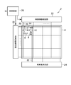
- FIG. 1 is a schematic diagram illustrating a schematic configuration of an organic EL display device according to an embodiment of the present invention.
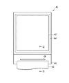
- FIG. 2 is a schematic plan view illustrating an example of a display panel of the organic EL display device illustrated in FIG. 1.
- FIG. 3 is a diagram showing an example of a III-III cross section of FIG.
- FIG. 3 is a schematic cross-sectional view illustrating an example of a state in which a touch panel is disposed on the display panel illustrated in FIG. 2.
- FIG. 1 is a schematic diagram showing a schematic configuration of an organic EL display device according to an embodiment of the present invention.
- the organic EL display device 2 includes a pixel array unit 4 that displays an image and a drive unit that drives the pixel array unit 4.
- the organic EL display device 2 has a display panel in which a laminated structure such as TFT and OLED is formed on a substrate.
- the schematic diagram shown in FIG. 1 is an example, and the present embodiment is not limited to this.
- OLEDs 6 and pixel circuits 8 are arranged in a matrix corresponding to the pixels.
- the pixel circuit 8 includes a plurality of TFTs 10 and 12 and a capacitor 14.
- the drive unit includes a scanning line drive circuit 20, a video line drive circuit 22, a drive power supply circuit 24, and a control device 26, and drives the pixel circuit 8 to control light emission of the OLED 6.
- the scanning line driving circuit 20 is connected to a scanning signal line 28 provided for each horizontal arrangement (pixel row) of pixels.
- the scanning line driving circuit 20 sequentially selects the scanning signal lines 28 according to the timing signal input from the control device 26, and applies a voltage for turning on the lighting TFT 10 to the selected scanning signal lines 28.
- the video line driving circuit 22 is connected to a video signal line 30 provided for each vertical arrangement (pixel column) of pixels.
- the video line driving circuit 22 receives a video signal from the control device 26, and in accordance with the selection of the scanning signal line 28 by the scanning line driving circuit 20, a voltage corresponding to the video signal of the selected pixel row is applied to each video signal line. Output to 30.
- the voltage is written into the capacitor 14 via the lighting TFT 10 in the selected pixel row.
- the driving TFT 12 supplies a current corresponding to the written voltage to the OLED 6, whereby the OLED 6 of the pixel corresponding to the selected scanning signal line 28 emits light.
- the drive power supply circuit 24 is connected to a drive power supply line 32 provided for each pixel column, and supplies current to the OLED 6 via the drive power supply line 32 and the drive TFT 12 of the selected pixel row.
- the lower electrode of the OLED 6 is connected to the driving TFT 12.
- the upper electrode of each OLED 6 is configured by an electrode common to the OLED 6 of all pixels.
- the lower electrode is configured as an anode (anode)
- the upper electrode is a cathode (cathode) and a low potential is input.
- the lower electrode is configured as a cathode (cathode)
- a low potential is input
- the upper electrode is an anode (anode) and a high potential is input.
- FIG. 2 is a schematic plan view showing an example of the display panel of the organic EL display device shown in FIG.
- the pixel array unit 4 shown in FIG. 1 is provided in the display area 42 of the display panel 40, and the OLEDs are arranged in the pixel array unit 4 as described above.
- the upper electrode 44 constituting the OLED 6 is formed in common for each pixel and covers the entire display region 42.
- a component mounting area 46 is provided on one side of the rectangular display panel 40, and wiring connected to the display area 42 is arranged.
- a driver integrated circuit (IC) 48 constituting a driving unit is mounted or an FPC 50 is connected.
- a flexible printed circuit board (FPC) 50 is connected to the control device 26 and other circuits 20, 22, 24, etc., and an IC is mounted thereon.
- FIG. 3 is a view showing an example of a section taken along the line III-III in FIG.
- the display panel 40 has a structure in which a circuit layer made of a TFT 72 and the like, an OLED 6 and a sealing layer 106 for sealing the OLED 6 are stacked on a substrate 70.
- substrate 70 is comprised with resin films, such as a glass plate and a polyimide resin, for example.
- the pixel array unit 4 is a top emission type, and the light generated by the OLED 6 is emitted to the side opposite to the substrate 70 side (upward in FIG. 3).
- the colorization system in the organic EL display device 2 is a color filter system, for example, it is disposed above the sealing layer 106. For example, red (R), green (G), and blue (B) light is produced by passing white light generated by the OLED 6 through the color filter.
- the pixel circuit 8 In the circuit layer of the display area 42, the pixel circuit 8, the scanning signal line 28, the video signal line 30, the drive power supply line 32, and the like are formed. At least a part of the driving unit can be formed as a circuit layer on the substrate 70 in a region adjacent to the display region 42. As described above, the driver IC 48 and the FPC 50 constituting the driving unit can be connected to the wiring 116 of the circuit layer in the component mounting region 46.
- a base layer 80 made of an inorganic insulating material is disposed on the substrate 70.
- the inorganic insulating material for example, silicon nitride (SiN y ), silicon oxide (SiO x ), and a composite thereof are used.
- a semiconductor region 82 serving as a channel portion and a source / drain portion of the top gate type TFT 72 is formed on the substrate 70 through the base layer 80.
- the semiconductor region 82 is made of, for example, polysilicon (p-Si).
- the semiconductor region 82 is formed, for example, by providing a semiconductor layer (p-Si film) on the substrate 70, patterning the semiconductor layer, and selectively leaving a portion used in the circuit layer.
- a gate electrode 86 is disposed on the channel portion of the TFT 72 via a gate insulating film 84.
- the gate insulating film 84 is typically formed of TEOS.
- the gate electrode 86 is formed by patterning a metal film formed by sputtering or the like, for example.
- An interlayer insulating layer 88 is disposed on the gate electrode 86 so as to cover the gate electrode 86.
- the interlayer insulating layer 88 is formed of, for example, the above inorganic insulating material. Impurities are introduced into the semiconductor region 82 (p-Si) serving as the source / drain portion of the TFT 72 by ion implantation, and further, a source electrode 90a and a drain electrode 90b electrically connected thereto are formed. Is done.
- An interlayer insulating film 92 is disposed on the TFT 72.
- a wiring 94 is disposed on the surface of the interlayer insulating film 92.
- the wiring 94 is formed by patterning a metal film formed by sputtering or the like.
- the metal film forming the wiring 94 and the metal film used for forming the gate electrode 86, the source electrode 90a, and the drain electrode 90b include, for example, the wiring 116 and the scanning signal line 28, the video signal line 30, and the like shown in FIG.
- the drive power supply line 32 can be formed with a multilayer wiring structure.
- a planarizing film 96 is formed of a resin material such as acrylic resin, and the OLED 6 is formed on the planarizing film 96 in the display region 42.
- the OLED 6 includes a lower electrode 100, an organic material layer 102, and an upper electrode 104.
- the organic material layer 102 includes a hole transport layer, a light emitting layer, an electron transport layer, and the like.
- the OLED 6 is typically formed by laminating the lower electrode 100, the organic material layer 102, and the upper electrode 104 in this order from the substrate 70 side.
- the lower electrode 100 is an anode (anode) of the OLED
- the upper electrode 104 is a cathode (cathode).
- the lower electrode 100 is connected to the source electrode 90a of the TFT 72.
- a contact hole 110 for connecting the lower electrode 100 to the TFT 72 is formed.
- a bank 112 for separating pixels is arranged on the above structure. For example, after the formation of the lower electrode 100, a bank 112 is formed at the pixel boundary, and the organic material layer 102 and the upper electrode 104 are stacked in an effective region (region where the lower electrode 100 is exposed) surrounded by the bank 112.
- the upper electrode 104 is typically formed of a transparent electrode material.
- a sealing layer 106 is disposed on the upper electrode 104.
- the sealing layer 106 can function as a protective layer that protects the OLED 6 from moisture or the like, and is formed so as to cover the entire display region 42.
- a protective layer may be disposed on the surface of the display region 42 in order to ensure the mechanical strength of the surface of the display panel 40.
- a protective layer is usually not provided in the component mounting area 46 in order to facilitate connection of an IC or FPC.
- the wiring of the FPC 50 and the terminal of the driver IC 48 are electrically connected to the wiring 116, for example.
- a configuration in which the touch panel is externally attached to the display panel (out-cell method) and the outside of the display panel (for example, between the display panel and a polarizing plate disposed outside the display panel)
- a configuration (on-cell method) provided and integrated in a display panel and a configuration (in-cell method) provided inside the display panel In this embodiment, an out-cell method or an on-cell method is adopted.
- the touch panel 60 is disposed on the sealing layer 106 of the display panel 40 and is stored in the housing of the organic EL display device 2 in this state. 4, the stacked structure excluding the sealing layer 106 on the substrate 70 in the stacked structure of the display panel 40 illustrated in FIG.
- the sealing layer 106 includes a first sealing layer 106a, a conductive layer 108, and a second sealing layer 106b in this order from the substrate 70 side.
- the conductive layer 108 does not exist at the end of the sealing layer 106 outside the display region 42, and the first sealing layer 106 a and the second sealing layer 106 b are in direct contact with each other. .
- the electromagnetic noise can be shielded at a position closer to the electromagnetic noise generation source (display unit), and the adverse effect due to the electromagnetic noise can be more reliably suppressed. For example, malfunction of the touch panel can be more reliably suppressed.
- the conductive layer can be formed during the sealing layer forming step, which can contribute to an improvement in manufacturing efficiency.
- Each of the first sealing layer (inorganic insulating layer) 106a and the second sealing layer (inorganic insulating layer) 106b is formed of an inorganic insulating material film such as SiN y by chemical vapor deposition (CVD), for example. For example, it is formed by forming a film with a thickness of about several ⁇ m.
- CVD chemical vapor deposition
- the conductive layer 108 is formed so that the sheet resistance is 500 ⁇ / ⁇ or less from the viewpoint of sufficiently obtaining a shielding effect of electromagnetic noise generated in the display portion (the structural layer 114 below the sealing layer 106). It is preferable.
- the conductive layer 108 is preferably formed so as to ensure transparency (for example, the visible light transmittance is 50% or more).
- the conductive layer 108 includes a conductive material.
- the conductive material include metals such as silver, gold, copper, and nickel, and alloys thereof (for example, Cu—Ni), metal oxides such as carbon and indium tin oxide (ITO), conductive polymers, and the like. It is done.
- the conductive layer 108 includes, for example, a binder resin such as an acrylic resin and the conductive material.
- the thickness of the conductive layer 108 is, for example, 10 ⁇ m to 50 ⁇ m.
- Any appropriate form can be adopted as the conductive material to be combined with the binder resin, but nanowires (typically metal nanowires) and / or nanotubes (typically carbon nanotubes) are preferably used.
- metal nanowires are particularly preferably used. This is because, for example, the above conductivity and transparency can be satisfactorily satisfied.
- the nanowire refers to a conductive material having a solid structure and a diameter of nanometer
- the nanotube refers to a conductive material having a hollow structure and a diameter of nanometer.
- Their thickness is, for example, 5 nm to 500 nm, preferably 5 nm to 50 nm. These lengths are, for example, 1 ⁇ m to 1000 ⁇ m, preferably 10 ⁇ m to 1000 ⁇ m.
- a coating material containing a binder resin and a conductive material is applied onto the first sealing layer 106a (for example, by an ink jet method), and post-processing (for example, heat treatment) according to the type of the binder resin (Curing treatment or photocuring treatment) is appropriately performed.
- the conductive layer 108 can also function as a planarization layer of the sealing layer 106.
- the present invention is not limited to the above embodiment, and various modifications can be made.
- it can be replaced with a configuration that is substantially the same as the configuration described in the above embodiment, a configuration that exhibits the same effects, or a configuration that can achieve the same purpose.
- the conductive layer 108 may be composed of, for example, an ITO film.
Landscapes
- Engineering & Computer Science (AREA)
- Theoretical Computer Science (AREA)
- General Engineering & Computer Science (AREA)
- Physics & Mathematics (AREA)
- General Physics & Mathematics (AREA)
- Human Computer Interaction (AREA)
- Microelectronics & Electronic Packaging (AREA)
- Optics & Photonics (AREA)
- Electroluminescent Light Sources (AREA)
- Devices For Indicating Variable Information By Combining Individual Elements (AREA)
Abstract
有機EL表示装置において、電磁ノイズによる悪影響をより確実に抑制する。 有機EL表示装置であって、基板と、前記基板の上に配置された複数の画素と、前記複数の画素を覆う第1の無機絶縁層と、前記第1の無機絶縁層の前記複数の画素とは反対側に位置し、前記複数の画素を覆う導電層と、前記導電層の前記第1の無機絶縁層とは反対側に位置し、前記複数の画素を覆う第2の無機絶縁層と、を有する。
Description
本発明は、有機EL表示装置に関する。
有機エレクトロルミネッセンス(EL)表示装置は、基板上に薄膜トランジスタ(TFT)や有機発光ダイオード(OLED)などが形成された表示パネルを有する。このような表示パネルは電磁ノイズを発生し、例えば、付加されたタッチパネルの誤作動を引き起こす場合がある。このような問題に対し、例えば、下記特許文献1では、タッチパネル部の基板や表示パネル部の基板にITO膜を形成することが提案されている。
しかし、電磁ノイズによる悪影響をより確実に抑制することが望まれている。
本発明は、上記に鑑み、電磁ノイズによる悪影響をより確実に抑制し得る有機EL表示装置の提供を目的とする。
本発明の有機EL表示装置は、基板と、前記基板の上に配置された複数の画素と、前記複数の画素を覆う第1の無機絶縁層と、前記第1の無機絶縁層の前記複数の画素とは反対側に位置し、前記複数の画素を覆う導電層と、前記導電層の前記第1の無機絶縁層とは反対側に位置し、前記複数の画素を覆う第2の無機絶縁層と、を有する。
1つの実施形態においては、上記第2の無機絶縁層の前記導電層とは反対の側にタッチパネルが配置される。
1つの実施形態においては、上記導電層のシート抵抗が500Ω/□以下である。
1つの実施形態においては、上記導電層の可視光透過率が50%以上である。
1つの実施形態においては、上記導電層はバインダー樹脂を含む。
1つの実施形態においては、上記導電層はナノワイヤおよび/またはナノチューブを含む。
1つの実施形態においては、上記導電層はITOを含む。
1つの実施形態においては、上記導電層は樹脂と導電性材料とを含む。
以下、本発明の実施形態について、図面を参照しつつ説明する。なお、図面については、同一又は同等の要素には同一の符号を付し、重複する説明は省略することがある。
図1は、本発明の実施形態に係る有機EL表示装置の概略の構成を示す模式図である。有機EL表示装置2は、画像を表示する画素アレイ部4と、画素アレイ部4を駆動する駆動部とを備える。有機EL表示装置2は、基板上にTFTやOLEDなどの積層構造が形成された表示パネルを有する。なお、図1に示した概略図は一例であって、本実施形態はこれに限定されるものではない。
画素アレイ部4には、画素に対応してOLED6および画素回路8がマトリクス状に配置される。画素回路8は複数のTFT10,12やキャパシタ14で構成される。
上記駆動部は、走査線駆動回路20、映像線駆動回路22、駆動電源回路24および制御装置26を含み、画素回路8を駆動しOLED6の発光を制御する。
走査線駆動回路20は、画素の水平方向の並び(画素行)ごとに設けられた走査信号線28に接続されている。走査線駆動回路20は、制御装置26から入力されるタイミング信号に応じて走査信号線28を順番に選択し、選択した走査信号線28に、点灯TFT10をオンする電圧を印加する。
映像線駆動回路22は、画素の垂直方向の並び(画素列)ごとに設けられた映像信号線30に接続されている。映像線駆動回路22は、制御装置26から映像信号を入力され、走査線駆動回路20による走査信号線28の選択に合わせて、選択された画素行の映像信号に応じた電圧を各映像信号線30に出力する。当該電圧は、選択された画素行にて点灯TFT10を介してキャパシタ14に書き込まれる。駆動TFT12は、書き込まれた電圧に応じた電流をOLED6に供給し、これにより、選択された走査信号線28に対応する画素のOLED6が発光する。
駆動電源回路24は、画素列ごとに設けられた駆動電源線32に接続され、駆動電源線32および選択された画素行の駆動TFT12を介してOLED6に電流を供給する。
ここで、OLED6の下部電極は、駆動TFT12に接続される。一方、各OLED6の上部電極は、全画素のOLED6に共通の電極で構成される。下部電極を陽極(アノード)として構成する場合は、高電位が入力され、上部電極は陰極(カソード)となって低電位が入力される。下部電極を陰極(カソード)として構成する場合は、低電位が入力され、上部電極は陽極(アノード)となって高電位が入力される。
図2は、図1に示す有機EL表示装置の表示パネルの一例を示す模式的な平面図である。表示パネル40の表示領域42に、図1に示した画素アレイ部4が設けられ、上述したように画素アレイ部4にはOLEDが配列される。上述したようにOLED6を構成する上部電極44は、各画素に共通に形成され、表示領域42全体を覆う。
矩形である表示パネル40の一辺には、部品実装領域46が設けられ、表示領域42につながる配線が配置される。部品実装領域46には、駆動部を構成するドライバ集積回路(IC)48が搭載されたり、FPC50が接続されたりする。フレキシブルプリント基板(FPC)50は、制御装置26やその他の回路20,22,24等に接続されたり、その上にICを搭載されたりする。
図3は、図2のIII-III断面の一例を示す図である。表示パネル40は、基板70の上にTFT72などからなる回路層、OLED6およびOLED6を封止する封止層106などが積層された構造を有する。基板70は、例えば、ガラス板、ポリイミド樹脂等の樹脂フィルムで構成される。本実施形態においては、画素アレイ部4はトップエミッション型であり、OLED6で生じた光は、基板70側とは反対側(図3において上向き)に出射される。なお、有機EL表示装置2におけるカラー化方式をカラーフィルタ方式とする場合には、例えば、封止層106よりも上側に配置される。このカラーフィルタに、OLED6にて生成した白色光を通すことで、例えば、赤(R)、緑(G)、青(B)の光を作る。
表示領域42の回路層には、上述した画素回路8、走査信号線28、映像信号線30、駆動電源線32などが形成される。駆動部の少なくとも一部分は、基板70上に回路層として表示領域42に隣接する領域に形成することができる。上述したように、駆動部を構成するドライバIC48やFPC50を、部品実装領域46にて、回路層の配線116に接続することができる。
図3に示すように、基板70上には、無機絶縁材料で形成された下地層80が配置される。無機絶縁材料としては、例えば、窒化シリコン(SiNy)、酸化シリコン(SiOx)およびこれらの複合体が用いられる。
表示領域42においては、下地層80を介して、基板70上には、トップゲート型のTFT72のチャネル部およびソース・ドレイン部となる半導体領域82が形成される。半導体領域82は、例えば、ポリシリコン(p-Si)で形成される。半導体領域82は、例えば、基板70上に半導体層(p-Si膜)を設け、この半導体層をパターニングし、回路層で用いる箇所を選択的に残すことにより形成される。TFT72のチャネル部の上には、ゲート絶縁膜84を介してゲート電極86が配置される。ゲート絶縁膜84は、代表的には、TEOSで形成される。ゲート電極86は、例えば、スパッタリング等で形成した金属膜をパターニングして形成される。ゲート電極86上には、ゲート電極86を覆うように層間絶縁層88が配置される。層間絶縁層88は、例えば、上記無機絶縁材料で形成される。TFT72のソース・ドレイン部となる半導体領域82(p-Si)には、イオン注入により不純物が導入され、さらにそれらに電気的に接続されたソース電極90aおよびドレイン電極90bが形成され、TFT72が構成される。
TFT72上には、層間絶縁膜92が配置される。層間絶縁膜92の表面には、配線94が配置される。配線94は、例えば、スパッタリング等で形成した金属膜をパターニングすることにより形成される。配線94を形成する金属膜と、ゲート電極86、ソース電極90aおよびドレイン電極90bの形成に用いた金属膜とで、例えば、配線116および図1に示した走査信号線28、映像信号線30、駆動電源線32を多層配線構造で形成することができる。この上に、例えば、アクリル系樹脂等の樹脂材料により平坦化膜96が形成され、表示領域42において、平坦化膜96上にOLED6が形成される。
OLED6は、下部電極100、有機材料層102および上部電極104を含む。有機材料層102は、具体的には、正孔輸送層、発光層、電子輸送層等を含む。OLED6は、代表的には、下部電極100、有機材料層102および上部電極104を基板70側からこの順に積層して形成される。本実施形態では、下部電極100がOLEDの陽極(アノード)であり、上部電極104が陰極(カソード)である。
図3に示すTFT72が、nチャネルを有した駆動TFT12であるとすると、下部電極100は、TFT72のソース電極90aに接続される。具体的には、上述した平坦化膜96の形成後、下部電極100をTFT72に接続するためのコンタクトホール110が形成され、例えば、平坦化膜96表面およびコンタクトホール110内に形成した導電体部をパターニングすることにより、TFT72に接続された下部電極100が画素ごとに形成される。
上記構造上には、画素を分離するバンク112が配置される。例えば、下部電極100の形成後、画素境界にバンク112を形成し、バンク112で囲まれた画素の有効領域(下部電極100の露出する領域)に、有機材料層102および上部電極104が積層される。上部電極104は、代表的には、透明電極材料で形成される。
上部電極104上には、封止層106が配置される。封止層106は、例えば、OLED6を水分等から保護する保護層として機能し得るため、表示領域42の全体を覆うように形成される。また、図示しないが、例えば、表示パネル40の表面の機械的な強度を確保するため、表示領域42の表面には保護層が配置され得る。この場合、部品実装領域46には、ICやFPCを接続し易くするため、通常、保護層を設けない。FPC50の配線やドライバIC48の端子は、例えば、配線116に電気的に接続される。
表示装置においてタッチパネルを搭載する際には、タッチパネルを表示パネルに外付けする構成(アウトセル方式)と、表示パネルの外部(例えば、表示パネルと表示パネルの外側に配置される偏光板との間)に設けて一体化する構成(オンセル方式)と、表示パネルの内部に設ける構成(インセル方式)とが知られている。本実施形態では、アウトセル方式もしくはオンセル方式が採用される。具体的には、図4に示すように、表示パネル40の封止層106上にタッチパネル60が配置され、この状態で、有機EL表示装置2の筐体に格納される。なお、図4において、図3に示す表示パネル40の積層構造のうち、基板70上の封止層106を除く積層構造を上部構造層114として簡略化して示している。
封止層106は、基板70側から、第1の封止層106a、導電層108および第2の封止層106bをこの順で含む。図示するように、表示領域42の外側の封止層106の端部では、導電層108は存在せず、第1の封止層106aと第2の封止層106bとが直に接している。このように、封止層106に導電層を含ませることで、電磁ノイズ発生源(表示部)により近い位置で電磁ノイズをシールドして、より確実に電磁ノイズによる悪影響を抑制することができる。例えば、タッチパネルの誤作動をより確実に抑制することができる。また、封止層の形成工程の際に導電層を形成することができ、製造効率の向上に寄与し得る。
第1の封止層(無機絶縁層)106aおよび第2の封止層(無機絶縁層)106bは、それぞれ、例えば、化学気相成長(CVD)法によりSiNy等の無機絶縁材料膜を、例えば、厚み数μm程度に成膜することにより形成される。このような封止層中に導電層108が挿入されることにより、換言すれば、導電層108の全体が第1の封止層106aと第2の封止層106bとによって覆われることにより、導電層108が他の部材に及ぼす悪影響を抑制し得る。導電層108は、表示領域42を被覆するように形成される。導電層108は、例えば、表示部(封止層106より下の構造層114)で発生する電磁ノイズのシールド効果を十分に得る観点から、そのシート抵抗が500Ω/□以下となるように形成されるのが好ましい。また、導電層108は、透明性を確保するように(例えば、可視光透過率が50%以上となるように)形成されることが好ましい。
導電層108は、導電性材料を含む。導電性材料としては、例えば、銀、金、銅、ニッケル等の金属およびこれらの合金(例えば、Cu-Ni)、カーボン、酸化インジウムスズ(ITO)等の金属酸化物、導電性ポリマー等が用いられる。
導電層108は、例えば、アクリル系樹脂等のバインダー樹脂および上記導電性材料を含む。この場合、導電層108の厚みは、例えば、10μm~50μmである。バインダー樹脂と組み合わせる導電性材料としては、任意の適切な形態が採用され得るが、ナノワイヤ(代表的には、金属ナノワイヤ)および/またはナノチューブ(代表的には、カーボンナノチューブ)が好ましく用いられる。中でも、金属ナノワイヤが特に好ましく用いられる。例えば、上記導電性および透明性を良好に満足し得るからである。ここで、ナノワイヤとは、中実構造の繊維状で、径がナノメートルサイズの導電性物質をいい、ナノチューブとは、中空構造の繊維状で、径がナノメートルサイズの導電性物質いう。これらの太さは、例えば5nm~500nmであり、好ましくは5nm~50nmである。これらの長さは、例えば1μm~1000μmであり、好ましくは10μm~1000μmである。導電層108は、例えば、バインダー樹脂と導電性材料を含む塗布物を第1の封止層106a上に塗布し(例えば、インクジェット方式により)、バインダー樹脂の種類に応じた後処理(例えば、熱硬化処理や光硬化処理)を適宜施すことにより形成される。導電層108は、封止層106の平坦化層としても機能し得る。
本発明は、上記実施形態に限定されるものではなく、種々の変形が可能である。例えば、上記実施形態で示した構成と実質的に同一の構成、同一の作用効果を奏する構成または同一の目的を達成することができる構成で置き換えることができる。具体的には、導電層108を、例えば、ITO膜で構成してもよい。
Claims (18)
- 基板と、
前記基板の上に配置された複数の画素と、
前記複数の画素を覆う第1の無機絶縁層と、
前記第1の無機絶縁層の前記複数の画素とは反対側に位置し、前記複数の画素を覆う導電層と、前記導電層の前記第1の無機絶縁層とは反対側に位置し、前記複数の画素を覆う第2の無機絶縁層と、
を有する有機EL表示装置。 - 前記基板の上に、前記複数の画素を含む表示領域が位置し、
前記第1の無機絶縁層と前記導電層と前記第2の無機絶縁層とは、前記表示領域を覆い、
前記第1の無機絶縁層の一部は、前記表示領域の外側に位置し、
前記第2の無機絶縁層の一部は、前記外側に位置し、
前記外側で、前記第1の無機絶縁層の端部と前記第2の無機絶縁層の端部とは、平面的に見て重なる、請求項1に記載の有機EL表示装置。 - 前記導電層の一部は、前記外側に位置し、
前記導電層の前記一部の端部は、前記第1の無機絶縁層の前記端部と前記表示領域との間に位置する、請求項2に記載の有機EL表示装置。 - 前記第1の無機絶縁層は、前記第2の無機絶縁層と直に接する領域を有し、
前記導電層の全体が、前記第1の無機絶縁層と前記第2の無機絶縁層とによって覆われている、請求項1に記載の有機EL表示装置。 - 前記複数の画素の各々は、下部電極と、前記下部電極の上の発光層と、前記発光層の上の上部電極とを有し、
前記第1の無機絶縁層は、前記上部電極の上に位置し、
前記第1の無機絶縁層と前記第2の無機絶縁層とは、前記発光層を封止する封止層である、請求項1に記載の有機EL表示装置。 - 前記第2の無機絶縁層の前記導電層とは反対の側に、タッチパネルが位置する、請求項1に記載の有機EL表示装置。
- 前記導電層はバインダー樹脂を含む、請求項1に記載の有機EL表示装置。
- 前記導電層はナノワイヤおよび/またはナノチューブを含む、請求項1に記載の有機EL表示装置。
- 前記導電層はITOを含む、請求項1に記載の有機EL表示装置。
- 前記導電層は、樹脂と導電性材料とを含む、請求項1に記載の有機EL表示装置。
- 前記導電層のシート抵抗が500Ω/□以下である、請求項1に記載の有機EL表示装置。
- 前記導電層の可視光透過率が50%以上である、請求項1に記載の有機EL表示装置。
- 各々が下部電極と、前記下部電極の上の発光層と、前記発光層の上の上部電極と、を有する複数の画素と、
前記上部電極の上に位置し、前記複数の画素を覆う第1の封止層と、
前記第1の封止層の前記複数の画素とは反対側に位置し、前記複数の画素を覆う導電層と、
前記導電層の前記第1の封止層とは反対側に位置し、前記複数の画素を覆う第2の封止層と、
前記第2の封止層の前記導電層とは反対側に位置するタッチパネルと、を有する有機EL表示装置。 - 前記第1の封止層は、前記第2の封止層と直に接する領域を有し、
前記導電層の全体が、前記第1の封止層と前記第2の封止層とによって覆われている、請求項13に記載の有機EL表示装置。 - 前記第1の封止層と前記導電層と前記第2の封止層とは、前記複数の画素を含む表示領域と、前記表示領域の外側とに跨って位置し、
前記外側で、前記第1の封止層の端部と前記第2の封止層の端部とは、平面的に見て重なる、請求項13に記載の有機EL表示装置。 - 前記外側に位置する前記導電層の端部は、前記第1の封止層の前記端部と前記表示領域との間に位置する、請求項15に記載の有機EL表示装置。
- 前記導電層はバインダー樹脂を含む、請求項13に記載の有機EL表示装置。
- 前記導電層はナノワイヤおよび/またはナノチューブを含む、請求項13に記載の有機EL表示装置。
Priority Applications (4)
| Application Number | Priority Date | Filing Date | Title |
|---|---|---|---|
| CN201880024831.9A CN110547045A (zh) | 2017-04-12 | 2018-01-23 | 有机el显示装置 |
| US16/596,883 US11031451B2 (en) | 2017-04-12 | 2019-10-09 | Organic EL display device |
| US17/148,680 US11335758B2 (en) | 2017-04-12 | 2021-01-14 | Display device and array substrate |
| US17/708,068 US11616110B2 (en) | 2017-04-12 | 2022-03-30 | Display device and array substrate |
Applications Claiming Priority (2)
| Application Number | Priority Date | Filing Date | Title |
|---|---|---|---|
| JP2017078826A JP2018181579A (ja) | 2017-04-12 | 2017-04-12 | 有機el表示装置 |
| JP2017-078826 | 2017-04-12 |
Related Child Applications (1)
| Application Number | Title | Priority Date | Filing Date |
|---|---|---|---|
| US16/596,883 Continuation US11031451B2 (en) | 2017-04-12 | 2019-10-09 | Organic EL display device |
Publications (1)
| Publication Number | Publication Date |
|---|---|
| WO2018189977A1 true WO2018189977A1 (ja) | 2018-10-18 |
Family
ID=63792452
Family Applications (1)
| Application Number | Title | Priority Date | Filing Date |
|---|---|---|---|
| PCT/JP2018/001951 Ceased WO2018189977A1 (ja) | 2017-04-12 | 2018-01-23 | 有機el表示装置 |
Country Status (4)
| Country | Link |
|---|---|
| US (3) | US11031451B2 (ja) |
| JP (1) | JP2018181579A (ja) |
| CN (1) | CN110547045A (ja) |
| WO (1) | WO2018189977A1 (ja) |
Cited By (1)
| Publication number | Priority date | Publication date | Assignee | Title |
|---|---|---|---|---|
| CN109979978A (zh) * | 2019-03-28 | 2019-07-05 | 云谷(固安)科技有限公司 | 显示装置、显示面板和电路板 |
Families Citing this family (4)
| Publication number | Priority date | Publication date | Assignee | Title |
|---|---|---|---|---|
| WO2019172423A1 (ja) * | 2018-03-09 | 2019-09-12 | 大日本印刷株式会社 | 導電性フィルム、センサー、タッチパネル、および画像表示装置 |
| KR102854035B1 (ko) * | 2018-12-28 | 2025-09-02 | 엘지디스플레이 주식회사 | 구동 회로 및 발광 소자를 포함하는 디스플레이 장치 |
| CN113299741B (zh) * | 2021-05-07 | 2022-09-09 | 惠州市华星光电技术有限公司 | 薄膜晶体管器件、背光模组和显示面板 |
| CN119677338A (zh) * | 2023-09-20 | 2025-03-21 | 合肥维信诺科技有限公司 | 显示面板和显示装置 |
Citations (4)
| Publication number | Priority date | Publication date | Assignee | Title |
|---|---|---|---|---|
| JP2013171454A (ja) * | 2012-02-21 | 2013-09-02 | Toppan Printing Co Ltd | 表示装置の電極パネルおよびその製造方法 |
| JP2014052997A (ja) * | 2011-11-11 | 2014-03-20 | Panasonic Corp | タッチパネル装置 |
| JP2014111335A (ja) * | 2012-12-05 | 2014-06-19 | Panasonic Corp | 導電層付き基材、電気素子及び有機エレクトロルミネッセンス素子 |
| JP2015011761A (ja) * | 2013-06-26 | 2015-01-19 | 株式会社ジャパンディスプレイ | Oled表示パネル |
Family Cites Families (14)
| Publication number | Priority date | Publication date | Assignee | Title |
|---|---|---|---|---|
| JP3885440B2 (ja) * | 1999-12-27 | 2007-02-21 | 凸版印刷株式会社 | 光電変換素子及びその製造方法 |
| JP2003099193A (ja) | 2001-09-21 | 2003-04-04 | Tohoku Pioneer Corp | 画面表示入力装置 |
| US8900366B2 (en) * | 2002-04-15 | 2014-12-02 | Samsung Display Co., Ltd. | Apparatus for depositing a multilayer coating on discrete sheets |
| JP2005353398A (ja) * | 2004-06-10 | 2005-12-22 | Toshiba Matsushita Display Technology Co Ltd | 表示素子、光学デバイス、及び光学デバイスの製造方法 |
| US7612498B2 (en) * | 2003-11-27 | 2009-11-03 | Toshiba Matsushita Display Technology Co., Ltd. | Display element, optical device, and optical device manufacturing method |
| JP2006004650A (ja) * | 2004-06-15 | 2006-01-05 | Toshiba Matsushita Display Technology Co Ltd | 表示素子及び光学デバイス |
| JP2011023558A (ja) * | 2009-07-16 | 2011-02-03 | Sharp Corp | 有機el表示装置 |
| BR112012002178A2 (pt) * | 2009-07-28 | 2016-05-31 | Sharp Kk | quadro de ligações, método para fabricação do mesmo, painel de exibição, e dispositivo de exibição |
| JPWO2013061967A1 (ja) * | 2011-10-27 | 2015-04-02 | コニカミノルタ株式会社 | 透明導電膜及び有機エレクトロルミネッセンス素子 |
| US20140111953A1 (en) * | 2012-10-19 | 2014-04-24 | Apple Inc. | Electronic Devices With Components Mounted to Touch Sensor Substrates |
| JP2014112510A (ja) * | 2012-11-02 | 2014-06-19 | Nitto Denko Corp | 透明導電性フィルム |
| DE102013106855B4 (de) * | 2013-07-01 | 2017-10-12 | Osram Oled Gmbh | Verfahren zum Herstellen eines optoelektronischen Bauelements und optoelektronisches Bauelement unter Verwendung einer flüssigen ersten Legierung |
| JP6371094B2 (ja) * | 2014-03-31 | 2018-08-08 | 株式会社ジャパンディスプレイ | 有機el表示装置 |
| KR102422103B1 (ko) * | 2015-05-28 | 2022-07-18 | 엘지디스플레이 주식회사 | 플렉서블 유기발광다이오드 표시장치 |
-
2017
- 2017-04-12 JP JP2017078826A patent/JP2018181579A/ja active Pending
-
2018
- 2018-01-23 CN CN201880024831.9A patent/CN110547045A/zh active Pending
- 2018-01-23 WO PCT/JP2018/001951 patent/WO2018189977A1/ja not_active Ceased
-
2019
- 2019-10-09 US US16/596,883 patent/US11031451B2/en active Active
-
2021
- 2021-01-14 US US17/148,680 patent/US11335758B2/en active Active
-
2022
- 2022-03-30 US US17/708,068 patent/US11616110B2/en active Active
Patent Citations (4)
| Publication number | Priority date | Publication date | Assignee | Title |
|---|---|---|---|---|
| JP2014052997A (ja) * | 2011-11-11 | 2014-03-20 | Panasonic Corp | タッチパネル装置 |
| JP2013171454A (ja) * | 2012-02-21 | 2013-09-02 | Toppan Printing Co Ltd | 表示装置の電極パネルおよびその製造方法 |
| JP2014111335A (ja) * | 2012-12-05 | 2014-06-19 | Panasonic Corp | 導電層付き基材、電気素子及び有機エレクトロルミネッセンス素子 |
| JP2015011761A (ja) * | 2013-06-26 | 2015-01-19 | 株式会社ジャパンディスプレイ | Oled表示パネル |
Cited By (2)
| Publication number | Priority date | Publication date | Assignee | Title |
|---|---|---|---|---|
| CN109979978A (zh) * | 2019-03-28 | 2019-07-05 | 云谷(固安)科技有限公司 | 显示装置、显示面板和电路板 |
| CN109979978B (zh) * | 2019-03-28 | 2020-10-20 | 云谷(固安)科技有限公司 | 显示装置、显示面板和电路板 |
Also Published As
| Publication number | Publication date |
|---|---|
| US20200044005A1 (en) | 2020-02-06 |
| CN110547045A (zh) | 2019-12-06 |
| JP2018181579A (ja) | 2018-11-15 |
| US20210134919A1 (en) | 2021-05-06 |
| US11616110B2 (en) | 2023-03-28 |
| US20220223676A1 (en) | 2022-07-14 |
| US11031451B2 (en) | 2021-06-08 |
| US11335758B2 (en) | 2022-05-17 |
Similar Documents
| Publication | Publication Date | Title |
|---|---|---|
| JP6456903B2 (ja) | 有機発光表示装置 | |
| CN100481562C (zh) | 发光装置和电子仪器 | |
| US11616110B2 (en) | Display device and array substrate | |
| KR102640114B1 (ko) | 유기발광 표시장치 | |
| US10134828B2 (en) | Display device and method of manufacturing a display device | |
| JP2014229356A (ja) | 発光素子およびその製造方法、ならびに表示装置 | |
| JP6397654B2 (ja) | 有機el発光装置 | |
| KR102427516B1 (ko) | 전계 발광 표시 장치 | |
| JP7320407B2 (ja) | 表示装置 | |
| CN110828518B (zh) | 显示装置、显示面板及其制造方法 | |
| CN104040613A (zh) | El显示装置以及使用于该el显示装置的布线基板 | |
| CN108010939B (zh) | 电致发光显示装置 | |
| JP2019003040A (ja) | 表示装置 | |
| WO2018220683A1 (ja) | 表示装置及び表示装置の製造方法 | |
| CN110476198B (zh) | 显示装置 | |
| US10861907B2 (en) | Display device and method of manufacturing a display device | |
| KR102935337B1 (ko) | 유기발광 표시장치 | |
| JP2019153551A (ja) | 有機el表示装置 | |
| JP7002629B2 (ja) | 素子基板 | |
| JP6387561B2 (ja) | 有機電界発光装置および電子機器 | |
| JP2018205583A (ja) | 表示装置 | |
| JP7086610B2 (ja) | 表示装置 | |
| JP2018106803A (ja) | 有機el表示装置および有機el表示装置の製造方法 | |
| CN100573905C (zh) | 发光装置和电子仪器 | |
| KR102632250B1 (ko) | 유기발광 표시장치 |
Legal Events
| Date | Code | Title | Description |
|---|---|---|---|
| 121 | Ep: the epo has been informed by wipo that ep was designated in this application |
Ref document number: 18784687 Country of ref document: EP Kind code of ref document: A1 |
|
| NENP | Non-entry into the national phase |
Ref country code: DE |
|
| 122 | Ep: pct application non-entry in european phase |
Ref document number: 18784687 Country of ref document: EP Kind code of ref document: A1 |