WO2018185571A1 - 有機化合物、発光素子、発光装置、電子機器、表示装置及び照明装置 - Google Patents
有機化合物、発光素子、発光装置、電子機器、表示装置及び照明装置 Download PDFInfo
- Publication number
- WO2018185571A1 WO2018185571A1 PCT/IB2018/051255 IB2018051255W WO2018185571A1 WO 2018185571 A1 WO2018185571 A1 WO 2018185571A1 IB 2018051255 W IB2018051255 W IB 2018051255W WO 2018185571 A1 WO2018185571 A1 WO 2018185571A1
- Authority
- WO
- WIPO (PCT)
- Prior art keywords
- light
- general formula
- group
- substituted
- organic compound
- Prior art date
- Legal status (The legal status is an assumption and is not a legal conclusion. Google has not performed a legal analysis and makes no representation as to the accuracy of the status listed.)
- Ceased
Links
- 0 *1c2cc(N(c3ccccc3)c3ccccc3)ccc2-c2c1ccc1c(c(c([o]3)c4)ccc4N(c4ccccc4)c4ccccc4)c3ccc21 Chemical compound *1c2cc(N(c3ccccc3)c3ccccc3)ccc2-c2c1ccc1c(c(c([o]3)c4)ccc4N(c4ccccc4)c4ccccc4)c3ccc21 0.000 description 11
- MABDZYHPJRPFNY-UHFFFAOYSA-N C(C1)C=Cc2c1[s]c1c2cccc1-c1cc(-c2cccc3c2[s]c2c3C=CCC2)cc(-c2cccc3c2[s]c2ccccc32)c1 Chemical compound C(C1)C=Cc2c1[s]c1c2cccc1-c1cc(-c2cccc3c2[s]c2c3C=CCC2)cc(-c2cccc3c2[s]c2ccccc32)c1 MABDZYHPJRPFNY-UHFFFAOYSA-N 0.000 description 1
- LBIWYKKLTXIMER-UHFFFAOYSA-N C1C=CC(c2c(ccc3c4NCC=C3c3ccccc3)c4ncc2)=CC1 Chemical compound C1C=CC(c2c(ccc3c4NCC=C3c3ccccc3)c4ncc2)=CC1 LBIWYKKLTXIMER-UHFFFAOYSA-N 0.000 description 1
- IFTRQJLVEBNKJK-UHFFFAOYSA-N CCC1CCCC1 Chemical compound CCC1CCCC1 IFTRQJLVEBNKJK-UHFFFAOYSA-N 0.000 description 1
- NRXFQFZTMHHYOB-UHFFFAOYSA-N ClC(CC1)=Cc2c1c1cc(cc3[o]c(cc(cc4)Cl)c4c3c3)c3cc1[o]2 Chemical compound ClC(CC1)=Cc2c1c1cc(cc3[o]c(cc(cc4)Cl)c4c3c3)c3cc1[o]2 NRXFQFZTMHHYOB-UHFFFAOYSA-N 0.000 description 1
- GBUPSYAYRGLKRW-RZMCKCCESA-N ClC1C=C[C@]1(COC1=C(C2CCC3Oc(cc(cc4)Cl)c4Br)c4ccccc4)[BrH]C1=CC2=C3c1ccccc1 Chemical compound ClC1C=C[C@]1(COC1=C(C2CCC3Oc(cc(cc4)Cl)c4Br)c4ccccc4)[BrH]C1=CC2=C3c1ccccc1 GBUPSYAYRGLKRW-RZMCKCCESA-N 0.000 description 1
- ONBQSJZFKGEABP-UHFFFAOYSA-N OC(C1c2ccccc2)C=Cc2c1ccc(O)c2C1=CC=CCC1 Chemical compound OC(C1c2ccccc2)C=Cc2c1ccc(O)c2C1=CC=CCC1 ONBQSJZFKGEABP-UHFFFAOYSA-N 0.000 description 1
- QBLXXNFCTBZBGU-UHFFFAOYSA-N OC(CC1C=C(c(ccc(Cl)c2)c2F)C(O)=CC1C1)=C1c(c(F)c1)ccc1Cl Chemical compound OC(CC1C=C(c(ccc(Cl)c2)c2F)C(O)=CC1C1)=C1c(c(F)c1)ccc1Cl QBLXXNFCTBZBGU-UHFFFAOYSA-N 0.000 description 1
- LLYNFNXDRXVJJX-UHFFFAOYSA-N c(cc1)ccc1N(c(cc1)cc(c2c3cccc2)c1[n]3-c1ccccc1)c1ccc2c(c(cc3)c(cc4)c5c3[o]c3cc(N(c6ccccc6)c(cc6c7c8cccc7)ccc6[n]8-c6ccccc6)ccc53)c4[o]c2c1 Chemical compound c(cc1)ccc1N(c(cc1)cc(c2c3cccc2)c1[n]3-c1ccccc1)c1ccc2c(c(cc3)c(cc4)c5c3[o]c3cc(N(c6ccccc6)c(cc6c7c8cccc7)ccc6[n]8-c6ccccc6)ccc53)c4[o]c2c1 LLYNFNXDRXVJJX-UHFFFAOYSA-N 0.000 description 1
Images


Classifications
-
- C—CHEMISTRY; METALLURGY
- C07—ORGANIC CHEMISTRY
- C07D—HETEROCYCLIC COMPOUNDS
- C07D307/00—Heterocyclic compounds containing five-membered rings having one oxygen atom as the only ring hetero atom
- C07D307/77—Heterocyclic compounds containing five-membered rings having one oxygen atom as the only ring hetero atom ortho- or peri-condensed with carbocyclic rings or ring systems
- C07D307/91—Dibenzofurans; Hydrogenated dibenzofurans
-
- C—CHEMISTRY; METALLURGY
- C07—ORGANIC CHEMISTRY
- C07D—HETEROCYCLIC COMPOUNDS
- C07D493/00—Heterocyclic compounds containing oxygen atoms as the only ring hetero atoms in the condensed system
- C07D493/02—Heterocyclic compounds containing oxygen atoms as the only ring hetero atoms in the condensed system in which the condensed system contains two hetero rings
- C07D493/04—Ortho-condensed systems
-
- C—CHEMISTRY; METALLURGY
- C07—ORGANIC CHEMISTRY
- C07D—HETEROCYCLIC COMPOUNDS
- C07D333/00—Heterocyclic compounds containing five-membered rings having one sulfur atom as the only ring hetero atom
- C07D333/50—Heterocyclic compounds containing five-membered rings having one sulfur atom as the only ring hetero atom condensed with carbocyclic rings or ring systems
- C07D333/76—Dibenzothiophenes
-
- C—CHEMISTRY; METALLURGY
- C07—ORGANIC CHEMISTRY
- C07D—HETEROCYCLIC COMPOUNDS
- C07D405/00—Heterocyclic compounds containing both one or more hetero rings having oxygen atoms as the only ring hetero atoms, and one or more rings having nitrogen as the only ring hetero atom
- C07D405/14—Heterocyclic compounds containing both one or more hetero rings having oxygen atoms as the only ring hetero atoms, and one or more rings having nitrogen as the only ring hetero atom containing three or more hetero rings
-
- C—CHEMISTRY; METALLURGY
- C07—ORGANIC CHEMISTRY
- C07D—HETEROCYCLIC COMPOUNDS
- C07D491/00—Heterocyclic compounds containing in the condensed ring system both one or more rings having oxygen atoms as the only ring hetero atoms and one or more rings having nitrogen atoms as the only ring hetero atoms, not provided for by groups C07D451/00 - C07D459/00, C07D463/00, C07D477/00 or C07D489/00
- C07D491/02—Heterocyclic compounds containing in the condensed ring system both one or more rings having oxygen atoms as the only ring hetero atoms and one or more rings having nitrogen atoms as the only ring hetero atoms, not provided for by groups C07D451/00 - C07D459/00, C07D463/00, C07D477/00 or C07D489/00 in which the condensed system contains two hetero rings
- C07D491/04—Ortho-condensed systems
- C07D491/044—Ortho-condensed systems with only one oxygen atom as ring hetero atom in the oxygen-containing ring
- C07D491/048—Ortho-condensed systems with only one oxygen atom as ring hetero atom in the oxygen-containing ring the oxygen-containing ring being five-membered
-
- C—CHEMISTRY; METALLURGY
- C07—ORGANIC CHEMISTRY
- C07D—HETEROCYCLIC COMPOUNDS
- C07D495/00—Heterocyclic compounds containing in the condensed system at least one hetero ring having sulfur atoms as the only ring hetero atoms
-
- C—CHEMISTRY; METALLURGY
- C07—ORGANIC CHEMISTRY
- C07D—HETEROCYCLIC COMPOUNDS
- C07D495/00—Heterocyclic compounds containing in the condensed system at least one hetero ring having sulfur atoms as the only ring hetero atoms
- C07D495/02—Heterocyclic compounds containing in the condensed system at least one hetero ring having sulfur atoms as the only ring hetero atoms in which the condensed system contains two hetero rings
- C07D495/04—Ortho-condensed systems
-
- C—CHEMISTRY; METALLURGY
- C09—DYES; PAINTS; POLISHES; NATURAL RESINS; ADHESIVES; COMPOSITIONS NOT OTHERWISE PROVIDED FOR; APPLICATIONS OF MATERIALS NOT OTHERWISE PROVIDED FOR
- C09K—MATERIALS FOR MISCELLANEOUS APPLICATIONS, NOT PROVIDED FOR ELSEWHERE
- C09K11/00—Luminescent materials, e.g. electroluminescent or chemiluminescent
- C09K11/06—Luminescent materials, e.g. electroluminescent or chemiluminescent containing organic luminescent materials
-
- H—ELECTRICITY
- H10—SEMICONDUCTOR DEVICES; ELECTRIC SOLID-STATE DEVICES NOT OTHERWISE PROVIDED FOR
- H10K—ORGANIC ELECTRIC SOLID-STATE DEVICES
- H10K50/00—Organic light-emitting devices
- H10K50/10—OLEDs or polymer light-emitting diodes [PLED]
- H10K50/14—Carrier transporting layers
- H10K50/16—Electron transporting layers
-
- H—ELECTRICITY
- H10—SEMICONDUCTOR DEVICES; ELECTRIC SOLID-STATE DEVICES NOT OTHERWISE PROVIDED FOR
- H10K—ORGANIC ELECTRIC SOLID-STATE DEVICES
- H10K85/00—Organic materials used in the body or electrodes of devices covered by this subclass
- H10K85/60—Organic compounds having low molecular weight
- H10K85/631—Amine compounds having at least two aryl rest on at least one amine-nitrogen atom, e.g. triphenylamine
- H10K85/636—Amine compounds having at least two aryl rest on at least one amine-nitrogen atom, e.g. triphenylamine comprising heteroaromatic hydrocarbons as substituents on the nitrogen atom
-
- H—ELECTRICITY
- H10—SEMICONDUCTOR DEVICES; ELECTRIC SOLID-STATE DEVICES NOT OTHERWISE PROVIDED FOR
- H10K—ORGANIC ELECTRIC SOLID-STATE DEVICES
- H10K85/00—Organic materials used in the body or electrodes of devices covered by this subclass
- H10K85/60—Organic compounds having low molecular weight
- H10K85/649—Aromatic compounds comprising a hetero atom
- H10K85/657—Polycyclic condensed heteroaromatic hydrocarbons
- H10K85/6572—Polycyclic condensed heteroaromatic hydrocarbons comprising only nitrogen in the heteroaromatic polycondensed ring system, e.g. phenanthroline or carbazole
-
- H—ELECTRICITY
- H10—SEMICONDUCTOR DEVICES; ELECTRIC SOLID-STATE DEVICES NOT OTHERWISE PROVIDED FOR
- H10K—ORGANIC ELECTRIC SOLID-STATE DEVICES
- H10K85/00—Organic materials used in the body or electrodes of devices covered by this subclass
- H10K85/60—Organic compounds having low molecular weight
- H10K85/649—Aromatic compounds comprising a hetero atom
- H10K85/657—Polycyclic condensed heteroaromatic hydrocarbons
- H10K85/6574—Polycyclic condensed heteroaromatic hydrocarbons comprising only oxygen in the heteroaromatic polycondensed ring system, e.g. cumarine dyes
-
- H—ELECTRICITY
- H10—SEMICONDUCTOR DEVICES; ELECTRIC SOLID-STATE DEVICES NOT OTHERWISE PROVIDED FOR
- H10K—ORGANIC ELECTRIC SOLID-STATE DEVICES
- H10K85/00—Organic materials used in the body or electrodes of devices covered by this subclass
- H10K85/60—Organic compounds having low molecular weight
- H10K85/649—Aromatic compounds comprising a hetero atom
- H10K85/657—Polycyclic condensed heteroaromatic hydrocarbons
- H10K85/6576—Polycyclic condensed heteroaromatic hydrocarbons comprising only sulfur in the heteroaromatic polycondensed ring system, e.g. benzothiophene
-
- C—CHEMISTRY; METALLURGY
- C09—DYES; PAINTS; POLISHES; NATURAL RESINS; ADHESIVES; COMPOSITIONS NOT OTHERWISE PROVIDED FOR; APPLICATIONS OF MATERIALS NOT OTHERWISE PROVIDED FOR
- C09K—MATERIALS FOR MISCELLANEOUS APPLICATIONS, NOT PROVIDED FOR ELSEWHERE
- C09K2211/00—Chemical nature of organic luminescent or tenebrescent compounds
- C09K2211/10—Non-macromolecular compounds
- C09K2211/1003—Carbocyclic compounds
- C09K2211/1007—Non-condensed systems
-
- C—CHEMISTRY; METALLURGY
- C09—DYES; PAINTS; POLISHES; NATURAL RESINS; ADHESIVES; COMPOSITIONS NOT OTHERWISE PROVIDED FOR; APPLICATIONS OF MATERIALS NOT OTHERWISE PROVIDED FOR
- C09K—MATERIALS FOR MISCELLANEOUS APPLICATIONS, NOT PROVIDED FOR ELSEWHERE
- C09K2211/00—Chemical nature of organic luminescent or tenebrescent compounds
- C09K2211/10—Non-macromolecular compounds
- C09K2211/1003—Carbocyclic compounds
- C09K2211/1014—Carbocyclic compounds bridged by heteroatoms, e.g. N, P, Si or B
-
- C—CHEMISTRY; METALLURGY
- C09—DYES; PAINTS; POLISHES; NATURAL RESINS; ADHESIVES; COMPOSITIONS NOT OTHERWISE PROVIDED FOR; APPLICATIONS OF MATERIALS NOT OTHERWISE PROVIDED FOR
- C09K—MATERIALS FOR MISCELLANEOUS APPLICATIONS, NOT PROVIDED FOR ELSEWHERE
- C09K2211/00—Chemical nature of organic luminescent or tenebrescent compounds
- C09K2211/10—Non-macromolecular compounds
- C09K2211/1018—Heterocyclic compounds
- C09K2211/1025—Heterocyclic compounds characterised by ligands
- C09K2211/1029—Heterocyclic compounds characterised by ligands containing one nitrogen atom as the heteroatom
-
- C—CHEMISTRY; METALLURGY
- C09—DYES; PAINTS; POLISHES; NATURAL RESINS; ADHESIVES; COMPOSITIONS NOT OTHERWISE PROVIDED FOR; APPLICATIONS OF MATERIALS NOT OTHERWISE PROVIDED FOR
- C09K—MATERIALS FOR MISCELLANEOUS APPLICATIONS, NOT PROVIDED FOR ELSEWHERE
- C09K2211/00—Chemical nature of organic luminescent or tenebrescent compounds
- C09K2211/10—Non-macromolecular compounds
- C09K2211/1018—Heterocyclic compounds
- C09K2211/1025—Heterocyclic compounds characterised by ligands
- C09K2211/1088—Heterocyclic compounds characterised by ligands containing oxygen as the only heteroatom
-
- C—CHEMISTRY; METALLURGY
- C09—DYES; PAINTS; POLISHES; NATURAL RESINS; ADHESIVES; COMPOSITIONS NOT OTHERWISE PROVIDED FOR; APPLICATIONS OF MATERIALS NOT OTHERWISE PROVIDED FOR
- C09K—MATERIALS FOR MISCELLANEOUS APPLICATIONS, NOT PROVIDED FOR ELSEWHERE
- C09K2211/00—Chemical nature of organic luminescent or tenebrescent compounds
- C09K2211/10—Non-macromolecular compounds
- C09K2211/1018—Heterocyclic compounds
- C09K2211/1025—Heterocyclic compounds characterised by ligands
- C09K2211/1092—Heterocyclic compounds characterised by ligands containing sulfur as the only heteroatom
-
- H—ELECTRICITY
- H10—SEMICONDUCTOR DEVICES; ELECTRIC SOLID-STATE DEVICES NOT OTHERWISE PROVIDED FOR
- H10K—ORGANIC ELECTRIC SOLID-STATE DEVICES
- H10K50/00—Organic light-emitting devices
- H10K50/10—OLEDs or polymer light-emitting diodes [PLED]
- H10K50/14—Carrier transporting layers
- H10K50/15—Hole transporting layers
Definitions
- One embodiment of the present invention relates to an organic compound and a light-emitting element, a display module, a lighting module, a display device, a light-emitting device, an electronic device, and a lighting device each using the organic compound.
- one embodiment of the present invention is not limited to the above technical field.
- the technical field of one embodiment of the invention disclosed in this specification and the like relates to an object, a method, or a manufacturing method.
- one embodiment of the present invention relates to a process, a machine, a manufacture, or a composition (composition of matter).
- the technical field of one embodiment of the present invention disclosed in this specification more specifically includes a semiconductor device, a display device, a liquid crystal display device, a light-emitting device, a lighting device, a power storage device, a memory device, an imaging device, A driving method or a manufacturing method thereof can be given as an example.
- the organic EL element has a function-separated configuration in which a plurality of functions are assigned to different substances, but among them, there is a demand for light emitting materials, particularly light emission efficiency that affects power consumption, and light emission color for improving display quality. Is big.
- Patent Document 1 discloses an organic compound having a naphthobisbenzofuran skeleton.
- An object of one embodiment of the present invention is to provide a novel organic compound. Another object is to provide an organic compound that emits light with favorable chromaticity. Alternatively, an object is to provide an organic compound that exhibits blue light emission with favorable chromaticity. Alternatively, an object is to provide an organic compound with favorable light emission efficiency. Alternatively, an object is to provide an organic compound with high carrier transportability. Another object is to provide a highly reliable organic compound.
- Another object of one embodiment of the present invention is to provide a novel light-emitting element. Another object is to provide a light-emitting element with favorable light emission efficiency. Another object is to provide a light-emitting element having favorable chromaticity. Another object is to provide a light-emitting element that emits blue light with favorable chromaticity. Another object is to provide a light-emitting element with favorable lifetime. Another object is to provide a light-emitting element with low driving voltage.
- the present invention should solve any one of the above-mentioned problems.
- One embodiment of the present invention is an organic compound represented by General Formula (G1) below.
- B represents any one of a substituted or unsubstituted naphthobisbenzofuran skeleton, a substituted or unsubstituted naphthobisbenzothiophene skeleton, and a substituted or unsubstituted naphthobenzofuranobenzothiophene skeleton.
- Ar 1 represents a substituted or unsubstituted aromatic hydrocarbon group having 6 to 25 carbon atoms, a substituted or unsubstituted dibenzofuranyl group, a substituted or unsubstituted dibenzothiophenyl group, and a substituted or unsubstituted carbazolyl group. One of them.
- A is any one of a substituted or unsubstituted dibenzofuranyl group, a substituted or unsubstituted dibenzothiophenyl group, and a substituted or unsubstituted carbazolyl group, and ⁇ 1 to ⁇ 3 are each independently substituted or unsubstituted.
- a divalent aromatic hydrocarbon group having 6 to 25 carbon atoms.
- L, m, and n each independently represent an integer of 0 to 2, and q is 1 or 2.
- Another embodiment of the present invention is an organic compound represented by General Formula (G1) below.
- B represents either a substituted or unsubstituted naphthobisbenzofuran skeleton, a substituted or unsubstituted naphthobisbenzothiophene skeleton, and a substituted or unsubstituted naphthobenzofuranobenzothiophene skeleton.
- Ar 1 is any one of a substituted or unsubstituted aromatic hydrocarbon group having 6 to 25 carbon atoms or a group represented by the following general formulas (g1) to (g3), and A represents the following general formula ( any one of groups represented by g1) to (g3).
- ⁇ 1 to ⁇ 3 are each independently a substituted or unsubstituted divalent aromatic hydrocarbon group having 6 to 25 carbon atoms.
- L, m, and n each independently represents an integer of 0 to 2, and q is 1 or 2.
- any one of R 1 to R 9 represents a single bond, and the rest each independently represents hydrogen, a hydrocarbon group having 1 to 10 carbon atoms, or 3 to 3 carbon atoms. It represents either a 10 cyclic hydrocarbon group or a substituted or unsubstituted aromatic hydrocarbon group having 6 to 14 carbon atoms.
- A is a group represented by the general formula (g3) and R 9 in the group represented by the general formula (g3) represents a single bond
- n is 1 or 2.
- Ar 1 is a group represented by the general formula (g3) and R 9 represents a single bond in (g3)
- m is 1 or 2.
- any one of R 1 to R 3 is a single bond
- a and / or Ar 1 is a group represented by general formula (g3).
- R 2 or R 3 is a single bond in the group represented by the general formula (g3).
- the A is a group represented by the general formula (g1) or the general formula (g3), and the general formula (g1) or the general formula ( R 2 in the group represented by g3) is an organic compound representing a single bond.
- Another embodiment of the present invention is an organic compound in which n is 0 in the above structure.
- Another embodiment of the present invention is an organic compound having the above structure, in which the Ar 1 is a substituted or unsubstituted aromatic hydrocarbon group having 6 to 25 carbon atoms.
- Another embodiment of the present invention is an organic compound in which 1 is 0 in the above structure.
- Another embodiment of the present invention is an organic compound in the above structure, in which the B is any one of the skeletons represented by the following general formulas (B1) to (B4).
- any one or two of R 10 to R 21 represent a single bond, and the rest each independently represents hydrogen, a hydrocarbon group having 1 to 10 carbon atoms, or 3 to 10 carbon atoms. Or a substituted or unsubstituted aromatic hydrocarbon group having 6 to 14 carbon atoms, or a substituted or unsubstituted diarylamino group having 12 to 32 carbon atoms.
- any one or two of R 30 to R 41 represent a single bond, and the rest each independently represent hydrogen, a hydrocarbon group having 1 to 10 carbon atoms, or 3 to 10 carbon atoms. Or a substituted or unsubstituted aromatic hydrocarbon group having 6 to 14 carbon atoms, or a substituted or unsubstituted diarylamino group having 12 to 32 carbon atoms.
- any one or two of R 50 to R 61 represent a single bond, and the rest each independently represents hydrogen, a hydrocarbon group having 1 to 10 carbon atoms, or 3 to 10 carbon atoms.
- any one or two of R 70 to R 81 represent a single bond, and the remaining are each independently hydrogen, a hydrocarbon group having 1 to 10 carbon atoms, or 3 to 10 carbon atoms.
- Another embodiment of the present invention is an organic compound in which, in the above structure, B is any of the skeletons represented by the general formulas (B1) to (B3).
- Another embodiment of the present invention is an organic compound in the above structure, in which the B is a skeleton represented by the following general formula (B1).
- X 2 and X 3 each independently represent an oxygen atom or a sulfur atom.
- R 10 to R 21 each represents 1 or 2 represents a single bond, and the rest each independently represents hydrogen, a hydrocarbon group having 1 to 10 carbon atoms, a cyclic hydrocarbon group having 3 to 10 carbon atoms, or a substituent. Alternatively, it represents either an unsubstituted aromatic hydrocarbon group having 6 to 14 carbon atoms or a substituted or unsubstituted diarylamino group having 12 to 32 carbon atoms.
- Another embodiment of the present invention is an organic compound in which any one or two of R 11 , R 12 , R 17, and R 18 in the general formula (B1) represent a single bond in the above structure.
- q in the general formula (G1) is 2, and either R 11 or R 12 in the general formula (B1) is a single bond. It is an organic compound in which either one of R 17 and R 18 is a single bond.
- Another embodiment of the present invention is an organic compound having the above structure, in which q in the general formula (G1) is 2, and R 11 and R 17 in the general formula (B1) are single bonds.
- Another embodiment of the present invention is an organic compound in which, in the above structure, q in the general formula (G1) is 2, and R 12 and R 18 in the general formula (B1) are single bonds.
- Another embodiment of the present invention is an organic compound having the above structure, in which the B is a skeleton represented by the following general formula (B2).
- X 2 and X 3 each independently represent an oxygen atom or a sulfur atom.
- R 30 to R 41 each represents 1 or 2 represents a single bond, and the rest each independently represents hydrogen, a hydrocarbon group having 1 to 10 carbon atoms, a cyclic hydrocarbon group having 3 to 10 carbon atoms, or a substituent. Alternatively, it represents either an unsubstituted aromatic hydrocarbon group having 6 to 14 carbon atoms or a substituted or unsubstituted diarylamino group having 12 to 32 carbon atoms.
- Another embodiment of the present invention is an organic compound in which any one or two of R 31 , R 32 , R 37, and R 38 in the general formula (B2) represent a single bond in the above structure.
- q in the general formula (G1) is 2, and R 31 or R 32 and R 37 or R 38 in the general formula (B2) are single bonds. It is an organic compound.
- Another embodiment of the present invention is an organic compound having the above structure, in which q in the general formula (G1) is 2, and R 31 and R 37 in the general formula (B2) are single bonds.
- Another embodiment of the present invention is an organic compound in which q in the general formula (G1) is 2 and R 32 and R 38 in the general formula (B2) are single bonds in the above structure.
- Another embodiment of the present invention is an organic compound having the above structure, in which the B is a skeleton represented by the following general formula (B3).
- X 2 and X 3 each independently represent an oxygen atom or a sulfur atom.
- R 50 to R 61 each represents 1 or 2 represents a single bond, and the rest each independently represents hydrogen, a hydrocarbon group having 1 to 10 carbon atoms, a cyclic hydrocarbon group having 3 to 10 carbon atoms, or a substituent. Alternatively, it represents either an unsubstituted aromatic hydrocarbon group having 6 to 14 carbon atoms or a substituted or unsubstituted diarylamino group having 12 to 32 carbon atoms.
- Another embodiment of the present invention is an organic compound in which any one or two of R 51 , R 52 , R 57, and R 58 in the general formula (B3) represent a single bond in the above structure.
- q in the general formula (G1) is 2, and R 51 or R 52 and R 57 or R 58 in the general formula (B3) are single bonds. It is an organic compound.
- Another embodiment of the present invention is an organic compound having the above structure, in which q in the general formula (G1) is 2, and R 51 and R 57 in the general formula (B3) are single bonds.
- Another embodiment of the present invention is an organic compound in which, in the above structure, q in the general formula (G1) is 2, and R 52 and R 58 in the general formula (B3) are single bonds.
- Another embodiment of the present invention is an organic compound in which, in the above structure, both X 2 and X 3 are oxygen atoms.
- Another embodiment of the present invention is an organic compound in which A is a group represented by General Formula (g1) in the above structure.
- Another embodiment of the present invention is an organic compound represented by the following general formula (G1-1).
- B is group represented by the following general formula (B1-1) or (B3-1).
- Ar 1 is a substituted or unsubstituted aromatic hydrocarbon group having 6 to 25 carbon atoms
- A is a group represented by the following general formula (g0).
- M represents an integer of 0 to 2.
- ⁇ 2 is a substituted or unsubstituted divalent aromatic hydrocarbon group having 6 to 14 carbon atoms.
- X 2 and X 3 each independently represent an oxygen atom or a sulfur atom.
- R 12 , R 18 , R 52 and R 58 represent a single bond.
- X 0 is an oxygen atom or a nitrogen atom to which a substituted or unsubstituted phenyl group is bonded.
- R 2 represents a single bond.
- Another embodiment of the present invention is the organic compound having a molecular weight of 1300 or less in the above structure.
- Another embodiment of the present invention is an organic compound having a molecular weight of 1000 or less in the above structure.
- Another embodiment of the present invention is a light-emitting element including the organic compound having the above structure.
- another embodiment of the present invention is represented by any one of the following structural formulas (iii), (vii), (ix), (x), (xi), (xiii), and (xv) to (XXiv). It is a light emitting element containing the organic compound.
- One embodiment of the present invention is a light-emitting device including the light-emitting element having the above structure and a transistor or a substrate.
- Another embodiment of the present invention is an electronic device including the light-emitting device having the above structure and a sensor, an operation button, a speaker, or a microphone.
- Another embodiment of the present invention is a lighting device including the light-emitting device having the above structure and a housing.
- another embodiment of the present invention is a light-emitting device including a light-emitting element having the above structure, a substrate, and a transistor.
- another embodiment of the present invention is an electronic device including the light-emitting device having the above structure and a sensor, an operation button, a speaker, or a microphone.
- another embodiment of the present invention is a lighting device including the light-emitting device having the above structure and a housing.
- the light-emitting device in this specification includes an image display device using a light-emitting element.
- a connector for example, an anisotropic conductive film or TCP (Tape Carrier Package) attached to a light emitting element, a module provided with a printed wiring board at the end of TCP, or a COG (Chip On Glass) method for a light emitting element.
- a module on which an IC (integrated circuit) is directly mounted is included in the light emitting device.
- a lighting fixture or the like may include a light emitting device.
- a novel organic compound can be provided.
- an organic compound exhibiting light emission with favorable chromaticity can be provided.
- an organic compound that exhibits blue light emission with favorable chromaticity can be provided.
- an organic compound with favorable emission efficiency can be provided.
- an organic compound with high carrier transportability can be provided.
- an organic compound with favorable reliability can be provided.
- a novel light-emitting element can be provided.
- a light-emitting element with favorable light emission efficiency can be provided.
- a light-emitting element having favorable chromaticity can be provided.
- a light-emitting element that emits blue light with favorable chromaticity can be provided.
- a light-emitting element with favorable lifetime can be provided.
- a light-emitting element with low driving voltage can be provided.
- a light-emitting device, an electronic device, and a display device with low power consumption can be provided.
- a highly reliable light-emitting device, electronic device, and display device can be provided.
- a light-emitting device, an electronic device, and a display device each having favorable display quality can be provided.
- FIG. 10 illustrates an electronic device.
- the figure showing a light source device The figure showing an illuminating device.
- FIG. 10 illustrates an electronic device.
- the figure showing a light source device The figure showing an illuminating device.
- FIG. 10 illustrates an electronic device.
- FIG. 10 illustrates an electronic device.
- 1 H NMR spectrum of 3,10FrA2Nbf (IV). Absorption spectrum and emission spectrum of 3,10FrA2Nbf (IV) in a toluene solution. The absorption spectrum and emission spectrum in the thin film state of 3,10FrA2Nbf (IV).
- MS spectrum of 3,10FrA2Nbf (IV). 1 H NMR spectrum of 2,9PCA2Nbf (III). The absorption spectrum and emission spectrum in the toluene solution of 2,9PCA2Nbf (III). The absorption spectrum and emission spectrum in a thin film state of 2,9PCA2Nbf (III). MS spectrum of 2,9PCA2Nbf (III).
- FIG. 6 shows luminance-current density characteristics of the light-emitting element 1 and the comparative light-emitting element 1.
- FIG. 9 shows current efficiency-luminance characteristics of the light-emitting element 1 and the comparative light-emitting element 1.
- FIG. 4 shows luminance-voltage characteristics of the light-emitting element 1 and the comparative light-emitting element 1.
- FIG. 6 shows current-voltage characteristics of the light-emitting element 1 and the comparative light-emitting element 1.
- FIG. 6 shows power efficiency-luminance characteristics of the light-emitting element 1 and the comparative light-emitting element 1.
- FIG. 6 shows external quantum efficiency-luminance characteristics of the light-emitting element 1 and the comparative light-emitting element 1.
- 2 shows emission spectra of the light-emitting element 1 and the comparative light-emitting element 1.
- FIG. 6 shows normalized luminance-time change characteristics of the light-emitting element 1 and the comparative light-emitting element 1.
- FIG. 11 shows luminance-current density characteristics of the light-emitting element 2 and the comparative light-emitting element 2;
- FIG. 6 shows current efficiency-luminance characteristics of the light-emitting element 2 and the comparative light-emitting element 2.
- FIG. 10 shows luminance-voltage characteristics of the light-emitting element 2 and the comparative light-emitting element 2.
- FIG. 6 shows current-voltage characteristics of the light-emitting element 2 and the comparative light-emitting element 2.
- FIG. 6 shows power efficiency-luminance characteristics of the light-emitting element 2 and the comparative light-emitting element 2.
- FIG. 6 shows external quantum efficiency-luminance characteristics of the light-emitting element 2 and the comparative light-emitting element 2.
- 2 shows emission spectra of the light-emitting element 2 and the comparative light-emitting element 2.
- FIG. 5 is a graph showing normalized luminance-time change characteristics of the light-emitting element 2 and the comparative light-emitting element 2;
- FIG. 11 shows luminance-current density characteristics of the light-emitting element 3 and the comparative light-emitting element 3.
- FIG. 6 shows current efficiency-luminance characteristics of the light-emitting element 3 and the comparative light-emitting element 3.
- FIG. 6 shows luminance-voltage characteristics of the light-emitting element 3 and the comparative light-emitting element 3.
- FIG. 6 shows current-voltage characteristics of the light-emitting element 3 and the comparative light-emitting element 3.
- FIG. 6 is a graph showing power efficiency-luminance characteristics of the light-emitting element 3 and the comparative light-emitting element 3.
- FIG. 6 shows external quantum efficiency-luminance characteristics of the light-emitting element 3 and the comparative light-emitting element 3.
- 2 shows emission spectra of the light-emitting element 3 and the comparative light-emitting element 3.
- FIG. 5 is a graph showing normalized luminance-time change characteristics of the light-emitting element 3 and the comparative light-emitting element 3;
- FIG. 11 shows luminance-current density characteristics of the light-emitting element 4 and the comparative light-emitting element 4.
- FIG. 6 shows current efficiency-luminance characteristics of the light-emitting element 4 and the comparative light-emitting element 4.
- FIG. 6 shows luminance-voltage characteristics of the light-emitting element 4 and the comparative light-emitting element 4.
- FIG. 6 shows current-voltage characteristics of the light-emitting element 4 and the comparative light-emitting element 4.
- FIG. 6 is a graph showing power efficiency-luminance characteristics of the light-emitting element 4 and the comparative light-emitting element 4.
- FIG. 6 shows external quantum efficiency-luminance characteristics of the light-emitting element 4 and the comparative light-emitting element 4.
- FIG. 6 is a graph showing normalized luminance-time change characteristics of the light-emitting element 4 and the comparative light-emitting element 4;
- FIG. 6 shows luminance-current density characteristics of the light-emitting element 5 and the comparative light-emitting element 5.
- FIG. 6 shows current efficiency-luminance characteristics of the light-emitting element 5 and the comparative light-emitting element 5.
- FIG. 6 shows luminance-voltage characteristics of the light-emitting element 5 and the comparative light-emitting element 5.
- FIG. 6 shows current-voltage characteristics of the light-emitting element 5 and the comparative light-emitting element 5.
- FIG. 6 shows power efficiency-luminance characteristics of the light-emitting element 5 and the comparative light-emitting element 5.
- FIG. 6 shows external quantum efficiency-luminance characteristics of the light-emitting element 5 and the comparative light-emitting element 5. The emission spectra of the light-emitting element 5 and the comparative light-emitting element 5.
- FIG. 6 shows current efficiency-luminance characteristics of the light-emitting element 5 and the comparative light-emitting element 5.
- FIG. 6 shows luminance-voltage characteristics of the light-emitting element 5 and the comparative light-emitting element 5.
- FIG. 6 shows current
- FIG. 5 is a graph showing normalized luminance-time change characteristics of the light-emitting element 5 and the comparative light-emitting element 5;
- FIG. 11 shows luminance-current density characteristics of the light-emitting element 6 and the comparative light-emitting element 6.
- FIG. 6 shows current efficiency-luminance characteristics of the light-emitting element 6 and the comparative light-emitting element 6.
- FIG. 6 shows luminance-voltage characteristics of the light-emitting element 6 and the comparative light-emitting element 6.
- FIG. 6 shows current-voltage characteristics of the light-emitting element 6 and the comparative light-emitting element 6.
- FIG. 6 shows power efficiency-luminance characteristics of the light-emitting element 6 and the comparative light-emitting element 6.
- FIG. 11 shows luminance-current density characteristics of the light-emitting element 6 and the comparative light-emitting element 6.
- FIG. 6 shows current efficiency-luminance characteristics of the light-emitting element 6 and the comparative light
- FIG. 6 shows external quantum efficiency-luminance characteristics of the light-emitting element 6 and the comparative light-emitting element 6.
- 2 shows emission spectra of the light-emitting element 6 and the comparative light-emitting element 6.
- FIG. 6 shows normalized luminance-time change characteristics of the light-emitting element 6 and the comparative light-emitting element 6.
- FIG. 11 shows luminance-current density characteristics of the light-emitting element 7.
- FIG. 11 shows current efficiency-luminance characteristics of the light-emitting element 7.
- FIG. 14 shows luminance-voltage characteristics of the light-emitting element 7.
- FIG. 14 shows current-voltage characteristics of the light-emitting element 7.
- FIG. 14 shows power efficiency-luminance characteristics of the light-emitting element 7.
- FIG. 14 shows external quantum efficiency-luminance characteristics of the light-emitting element 7.
- FIG. 10 shows normalized luminance-time change characteristics of the light-emitting element 7;
- FIG. 11 shows luminance-current density characteristics of the light-emitting element 8.
- FIG. 11 shows current efficiency-luminance characteristics of the light-emitting element 8.
- FIG. 14 shows luminance-voltage characteristics of the light-emitting element 8.
- FIG. 14 shows current-voltage characteristics of the light-emitting element 8;
- FIG. 10 shows power efficiency-luminance characteristics of the light-emitting element 8.
- FIG. 14 shows external quantum efficiency-luminance characteristics of the light-emitting element 8.
- FIG. 10 shows normalized luminance-time change characteristics of the light-emitting element 8;
- FIG. 9 shows luminance-current density characteristics of the light-emitting element 9;
- FIG. 10 shows current efficiency-luminance characteristics of the light-emitting element 9;
- FIG. 11 shows luminance-voltage characteristics of the light-emitting element 9;
- FIG. 14 shows current-voltage characteristics of the light-emitting element 9;
- FIG. 10 shows power efficiency-luminance characteristics of the light-emitting element 9;
- FIG. 14 shows external quantum efficiency-luminance characteristics of the light-emitting element 9.
- FIG. 9 shows normalized luminance-time change characteristics of the light-emitting element 9;
- FIG. 16 shows luminance-current density characteristics of the light-emitting elements 10 to 15.
- FIG. 14 shows current efficiency-luminance characteristics of the light-emitting elements 10 to 15.
- FIG. 14 shows luminance-voltage characteristics of the light-emitting elements 10 to 15.
- FIG. 14 shows current-voltage characteristics of the light-emitting elements 10 to 15.
- FIG. 14 shows power efficiency-luminance characteristics of the light-emitting elements 10 to 15.
- FIG. 14 shows external quantum efficiency-luminance characteristics of the light-emitting elements 10 to 15.
- 10 shows emission spectra of the light-emitting elements 10 to 15.
- FIG. 10 shows normalized luminance-time change characteristics of the light-emitting elements 10 to 15;
- the organic compound of one embodiment of the present invention is an organic compound represented by the following general formula (G1).
- B represents any of a substituted or unsubstituted naphthobisbenzofuran skeleton, a substituted or unsubstituted naphthobisbenzothiophene skeleton, and a substituted or unsubstituted naphthobenzofuranobenzothiophene skeleton.
- 1 or 2 substituted or unsubstituted arylamino group is bonded to the skeleton B (that is, q is 1 or 2)
- the arylamine is not an amine having only a simple aryl group such as a phenyl group, but is substituted.
- an arylamine having at least one of an unsubstituted dibenzofuranyl group, a substituted or unsubstituted dibenzothiophenyl group, and a substituted or unsubstituted carbazolyl group.
- A represents any one of a substituted or unsubstituted dibenzofuranyl group, a substituted or unsubstituted dibenzothiophenyl group, and a substituted or unsubstituted carbazolyl group.
- Ar 1 represents a substituted or unsubstituted aromatic hydrocarbon group having 6 to 25 carbon atoms, a substituted or unsubstituted dibenzofuranyl group, a substituted or unsubstituted dibenzothiophenyl group, and It represents either a substituted or unsubstituted carbazolyl group.
- ⁇ 1 , ⁇ 2 and ⁇ 3 are each independently a substituted or unsubstituted divalent aromatic hydrocarbon group having 6 to 25 carbon atoms, and l, m and n are each independently Any one of 0, 1 and 2 is taken.
- a substituted or unsubstituted naphthobisbenzofuran skeleton, a substituted or unsubstituted naphthobisbenzothiophene skeleton, or a substituted or unsubstituted naphthobenzofuranobenzothiophene skeleton is a very useful skeleton for a light emitting element. Since the organic compound has high emission efficiency and exhibits good blue light emission, a light-emitting element using the organic compound can be a blue light-emitting element with high emission efficiency.
- ITU-R BT is an international standard for an ultra-wide color gamut that conforms to 8K displays. . It is a very promising material as a blue light emitting material for expressing a color gamut covering the 2020 standard.
- the present inventors specially have in these skeletons at least one or more substituted or unsubstituted dibenzofuranyl groups, substituted or unsubstituted dibenzothiophenyl groups and substituted or unsubstituted carbazolyl groups as described above.
- the present inventors have found that a light-emitting element using an organic compound having an arylamine is a light-emitting element with better characteristics. Specifically, there are effects such as better luminous efficiency and even better color purity.
- Ar 1 or A or both represents a substituted or unsubstituted dibenzofuranyl group, a substituted or unsubstituted dibenzothiophenyl group, and a substituted or unsubstituted carbazolyl group. In some cases, these are preferably groups represented by the following general formulas (g1) to (g3).
- any one of R 1 to R 9 represents a single bond, and the rest are each independently hydrogen, a hydrocarbon group having 1 to 10 carbon atoms, It represents either a 3 to 10 cyclic hydrocarbon group or a substituted or unsubstituted aromatic hydrocarbon group having 6 to 14 carbon atoms.
- A is a group represented by the general formula (g3) and R 9 in the group represented by the general formula (g3) represents a single bond, n is 1 or 2.
- Ar 1 is a group represented by the general formula (g3) and R 9 in the group represented by the general formula (g3) represents a single bond, m is 1 or 2. To do.
- any one of R 1 to R 3 is preferably a single bond, and in the above general formula (g2)
- any one of R 1 to R 3 is preferably a single bond, and when it is a group represented by the general formula (g3), R 2 or R 3 is a single bond. Preferably there is.
- a in the general formula (G1) is a group represented by the general formula (g3) and R 9 is a single bond
- a configuration in which n is 0 has few synthesis steps, and a sublimation temperature. Is also preferable.
- l and n are 0 regardless of A, respectively, because the number of synthesis steps is small and the sublimation temperature is low.
- a in the general formula (G1) is a group represented by the general formula (g3) and R 9 is a single bond, a configuration in which n is 1 is easily synthesized and chemically stable. Therefore, it is preferable.
- Ar 1 is a group represented by the general formula (g3) and R 9 is a single bond, a configuration in which m is 1 is preferable for the same reason.
- a and Ar 1 in the general formula (G1) is a group represented by the general formula (g1) or a group represented by the general formula (g2), preferably the general formula ( The group represented by g1) is preferable because the organic compound represented by the general formula (G1) emits light at a short wavelength.
- the position of the single bond bonded to ⁇ 2 , ⁇ 3 , or nitrogen (amine) of the group represented by the general formula (g1) or the group represented by the general formula (g2) is R 1 or R 2 is preferable because it emits light at a shorter wavelength.
- the position of the single bond bonded to ⁇ 2 , ⁇ 3 , or nitrogen (amine) of the group represented by the general formula (g1) or the group represented by the general formula (g2) is R 2 or R 3 is preferable because the emission quantum yield is higher.
- the position of the single bond is R 2 because the emission spectrum is narrowed.
- Ar 1 and A in the general formula (G1) be a group represented by the general formula (g3) because reliability is improved.
- Ar 1 is preferably a substituted or unsubstituted aromatic hydrocarbon group having 6 to 25 carbon atoms because the sublimation temperature is lowered.
- q is preferably 2 because the emission quantum yield is increased. It is preferable that q is 1 because the sublimation temperature is lowered.
- the sublimation temperature includes the meaning of the evaporation temperature.
- Typical examples of the group represented by A in the general formula (G1) are shown in the following structural formulas (Ar-50) to (Ar-66). These further have a substituent such as a hydrocarbon group having 1 to 10 carbon atoms, a cyclic hydrocarbon group having 3 to 10 carbon atoms, or a substituted or unsubstituted aromatic hydrocarbon group having 6 to 14 carbon atoms. It may be.
- Ar 1 represents a substituted or unsubstituted aromatic hydrocarbon group having 6 to 25 carbon atoms, a substituted or unsubstituted dibenzofuranyl group, a substituted or unsubstituted dibenzothiophenyl group, and It represents either a substituted or unsubstituted carbazolyl group.
- Specific examples of the substituted or unsubstituted aromatic hydrocarbon group having 6 to 25 carbon atoms include phenyl group, biphenyl group, terphenyl group, naphthyl group, fluorenyl group, dimethylfluorenyl group, and spirofluorenyl group.
- Ar 1 Diphenylfluorenyl group, phenanthryl group, anthryl group, dihydroanthryl group, triphenylenyl group, pyrenyl group and the like.
- Representative examples of Ar 1 are shown in the following structural formulas (Ar-50) to (Ar-66), (Ar-100) to (Ar-119), and (Ar-130) to (Ar-140). These further have a substituent such as a hydrocarbon group having 1 to 10 carbon atoms, a cyclic hydrocarbon group having 3 to 10 carbon atoms, or a substituted or unsubstituted aromatic hydrocarbon group having 6 to 14 carbon atoms. It may be.
- the carbazolyl group is bonded to ⁇ 2 , ⁇ 3 , and nitrogen (amine) in the general formula (G1) at the 9th position.
- An organic compound having a structure is preferable because conjugation is difficult to extend and short wavelength light emission is obtained.
- An organic compound having a structure in which a carbazolyl group is bonded at the 3-position, an organic compound having a structure in which a dibenzofuranyl group is bonded at the 2-position, and an organic compound having a structure in which a dibenzothiophenyl group is bonded at the 2-position Is preferable because conjugation is easily extended, hole transportability is high, long-wavelength light emission is obtained, and reliability is good.
- the carbazolyl group is particularly effective.
- a carbazolyl group is bonded to ⁇ 2 , ⁇ 3 , and nitrogen (amine) in General Formula (G1) at the 2-position.
- An organic compound having a structure, an organic compound having a structure in which a dibenzofuranyl group is bonded at the 3-position, and an organic compound having a structure in which a dibenzothiophenyl group is bonded at the 3-position have a high carrier transport property and a driving voltage. Can be expected, which is preferable.
- the 9th position of the carbazolyl group has better reliability when an aryl group is bonded, etc. Since the effect of this is acquired, it is preferable.
- a dibenzofuranyl group is added to ⁇ 2 , ⁇ 3 , and nitrogen (amine) in the general formula (G1).
- an organic compound having a structure bonded to the 4-position and an organic compound having a structure bonded to the 4-position of a dibenzothiophenyl group is that the conjugation is not easily extended, the short wavelength emission is obtained, and the reliability is good. Therefore, it is preferable.
- a compound in which a phenyl group is linked as in (Ar-100) to (Ar-108) is preferable because the conjugation is difficult to extend and the emission wavelength is short.
- the number of condensed six-membered rings is two or less, such as a benzene ring, a naphthalene ring, and a fluorene ring, or six as in a phenanthrene ring. Even if the number of condensed rings of the member ring is 3 or more, the other six-membered ring is composed of a condensed ring only in the a-position, c-position and e-position with respect to the six-membered ring, It is preferable that conjugation is difficult to spread and light emission has a short wavelength.
- ⁇ 1 to ⁇ 3 in the general formula (G1) each independently represent a substituted or unsubstituted divalent aromatic hydrocarbon group having 6 to 25 carbon atoms, specifically, a phenylene group, a biphenylene group, Examples include a terphenylene group, a naphthylene group, a fluorenylene group, and a dimethylfluorenyl group.
- ⁇ 1 to ⁇ 3 groups represented by the following structural formulas (Ar-1) to (Ar-33) can be given.
- These further have a substituent such as a hydrocarbon group having 1 to 10 carbon atoms, a cyclic hydrocarbon group having 3 to 10 carbon atoms, or a substituted or unsubstituted aromatic hydrocarbon group having 6 to 14 carbon atoms. You may do it.
- a substituent such as a hydrocarbon group having 1 to 10 carbon atoms, a cyclic hydrocarbon group having 3 to 10 carbon atoms, or a substituted or unsubstituted aromatic hydrocarbon group having 6 to 14 carbon atoms. You may do it.
- ⁇ 1 to ⁇ 3, as in (Ar-1) to (Ar-11), are difficult to extend when a phenylene group or a group of several phenylene groups are connected, and the singlet excited level is kept high. It is preferable because it sags. In particular, a configuration including a metaphenylene group is preferable because the effect is remarkable. In addition, a structure in which ⁇ 1 to ⁇ 3 are paraphenylene groups is preferable because of high reliability as a light-emitting material. Moreover, when the substituent is connected with carbon having a sigma bond such as the 9th position of fluorene as in (Ar-24) to (Ar-27), the conjugation is difficult to extend and the S1 level is kept high. Therefore, the emission wavelength is preferably shorter.
- ⁇ 1 , ⁇ 2, and ⁇ 3 may be connected to different substituents.
- (Ar-17) and (Ar-18) are naphthylene and phenylene linked.
- a substituted or unsubstituted naphthobisbenzofuran skeleton a substituted or unsubstituted naphthobisbenzothiophene skeleton, or a substituted or unsubstituted naphthobenzofuranobenzothiophene represented by B
- the skeleton is preferably any of the skeletons represented by the following general formulas (B1) to (B4).
- X 2 and X 3 each independently represent an oxygen atom or a sulfur atom. These two atoms are preferably the same atom for the convenience of synthesis.
- the structure in which both are oxygen atoms is easy to synthesize, has high singlet excitation levels, can emit light with a shorter wavelength, and has a high emission quantum yield. Therefore, it is preferable.
- X 2 and X 3 emit light with a shorter wavelength as the number of oxygen atoms increases, and emit light with a longer wavelength as the number of sulfur atoms increases. Therefore, X 2 and X 3 can be arbitrarily set according to the target singlet excitation level or emission wavelength. You can choose.
- the organic compound represented by the general formula (G1) tends to change its emission wavelength depending on the skeleton represented by B, and B is a skeleton represented by the general formula (B2), which is represented by the general formula (B4).
- B is a skeleton represented by the general formula (B2), which is represented by the general formula (B4).
- the compound represented by the general formula (B2) is preferable.
- a compound represented by the general formula (B3) is preferable.
- the emission spectrum is narrowed and light emission with high color purity is emitted. Since it is obtained, it is preferable.
- any one or two of R 10 to R 21 represent a single bond, and the rest are each independently hydrogen, a hydrocarbon group having 1 to 10 carbon atoms, It represents any of a cyclic hydrocarbon group having 3 to 10 carbon atoms, a substituted or unsubstituted aromatic hydrocarbon group having 6 to 14 carbon atoms, and a substituted or unsubstituted diarylamino group having 12 to 32 carbon atoms.
- the single bond is preferably any one or two of R 11 , R 12 , R 17 and R 18 out of R 10 to R 21 because the synthesis is simple.
- R 11 or R 12 when any one of R 10 to R 21 is a single bond (that is, when q in the general formula (G1) is 2), either R 11 or R 12
- R 11 and R 17 are preferably single bonds from the viewpoint of obtaining long-wavelength light emission
- R 12 and R 18 are single bonds, so that short-wavelength light emission can be obtained and the emission quantum efficiency is good.
- the molar extinction coefficient is high, and the reliability when light is emitted is preferable.
- any one or two of R 30 to R 41 represent a single bond, and the rest each independently represent hydrogen, a hydrocarbon group having 1 to 10 carbon atoms, or 3 to 10 carbon atoms. Or a substituted or unsubstituted aromatic hydrocarbon group having 6 to 14 carbon atoms, or a substituted or unsubstituted diarylamino group having 12 to 32 carbon atoms.
- the single bond is preferably any one or two of R 31 , R 32 , R 37 and R 38 out of R 30 to R 41 because of easy synthesis.
- R 31 and R 32 when any two of R 30 to R 41 are a single bond (that is, when q in the general formula (G1) is 2), any one of R 31 and R 32
- one of R 37 and R 38 is preferably a single bond from the standpoint of ease of synthesis.
- R 31 and R 37 are preferably single bonds from the viewpoint of obtaining long-wavelength light emission, and if R 32 and R 38 are single bonds, short-wavelength light emission is obtained, and the emission quantum efficiency is good.
- the molar extinction coefficient is high, and the reliability when light is emitted is preferable.
- any one or two of R 50 to R 61 represent a single bond, and the rest each independently represents hydrogen, a hydrocarbon group having 1 to 10 carbon atoms, or 3 to 10 carbon atoms.
- the single bond is preferably any one or two of R 51 , R 52 , R 57 and R 58 out of R 50 to R 61 because synthesis is simple.
- R 51 or R 52 when any two of R 50 to R 61 are a single bond (that is, when q in the general formula (G1) is 2), either R 51 or R 52
- R 51 or R 52 it is preferable from the easiness of synthesis that either R 57 or R 58 is a single bond.
- R 51 and R 57 are preferably single bonds from the viewpoint of obtaining long-wavelength light emission, and if R 52 and R 58 are single bonds, short-wavelength light emission is obtained and the emission quantum efficiency is good.
- the molar extinction coefficient is high, and the reliability when light is emitted is preferable.
- any one or two of R 70 to R 81 represent a single bond, and the remaining are each independently hydrogen, a hydrocarbon group having 1 to 10 carbon atoms, or 3 to 10 carbon atoms. Or a substituted or unsubstituted aromatic hydrocarbon group having 6 to 14 carbon atoms, or a substituted or unsubstituted diarylamino group having 12 to 32 carbon atoms.
- the single bond is preferably any one or two of R 71 , R 72 , R 77 and R 78 out of R 70 to R 81 because synthesis is simple.
- R 71 and R 72 are preferably single bonds from the viewpoint of obtaining long-wavelength light emission
- R 72 and R 77 are single bonds, so that short-wavelength light emission can be obtained and the emission quantum efficiency is good.
- the molar extinction coefficient is high, and the reliability when light is emitted is preferable.
- a substituent is a single bond among the substituents represented by R 10 to R 21 , R 30 to R 41 , R 50 to R 61 , and R 70 to R 81.
- hydrogen is preferable because synthesis is simple and the sublimation temperature is low.
- heat resistance, solubility in a solvent, and the like can be improved, and an emission wavelength can be shifted to a long wavelength.
- organic compound represented by the general formula (G1) is preferably an organic compound represented by the following general formula (G1-1).
- B is group represented by the following general formula (B1-1) or (B3-1).
- Ar 1 is a substituted or unsubstituted aromatic hydrocarbon group having 6 to 25 carbon atoms
- A is a group represented by the following general formula (g0).
- M represents an integer of 0 to 2.
- ⁇ 2 is a substituted or unsubstituted divalent aromatic hydrocarbon group having 6 to 14 carbon atoms.
- X 2 and X 3 each independently represent an oxygen atom or a sulfur atom.
- R 12 , R 18 , R 52 and R 58 represent a single bond.
- X 0 is an oxygen atom or a nitrogen atom to which a substituted or unsubstituted phenyl group is bonded.
- R 2 represents a single bond.
- the molecular weight of the organic compound represented by the general formula (G1) or (G1-1) is 1300 or less, preferably 1000 or less in consideration of sublimation. In view of the film quality, the molecular weight is preferably 650 or more.
- the substituent when the skeleton or the group bonded to the above organic compound has a substituent, the substituent includes a hydrocarbon group having 1 to 10 carbon atoms, a cyclic hydrocarbon group having 3 to 10 carbon atoms, and 6 carbon atoms. It is preferably any one of 14 to 14 aromatic hydrocarbon groups.
- the hydrocarbon group having 1 to 10 carbon atoms may be methyl, ethyl, propyl, isopropyl, butyl, tert- Examples thereof include a butyl group, a pentyl group, a hexyl group, a heptyl group, an octyl group, a nonyl group, a decyl group, and an icosyl group.
- the cyclic hydrocarbon group having 3 to 10 carbon atoms include a cyclopropyl group and a cyclohexyl group.
- Examples of the aromatic hydrocarbon group having 6 to 14 carbon atoms include a phenyl group, a biphenyl group, a naphthyl group, a phenanthryl group, an anthryl group, and a fluorenyl group.
- the two aryl groups of the diarylamino group are each independently an aromatic hydrocarbon group having 6 to 16 carbon atoms. It is more preferable that Examples of the aromatic hydrocarbon group include a phenyl group, a biphenyl group, a naphthyl group, a phenanthryl group, an anthryl group, a fluorenyl group, and a naphthylphenyl group.
- the aromatic hydrocarbon group having 6 to 14 carbon atoms and the diarylamino group having 12 to 32 carbon atoms are further an aliphatic hydrocarbon group having 1 to 6 carbon atoms and an alicyclic group having 3 to 6 carbon atoms. You may have a hydrocarbon group etc. as a substituent.
- X 2 and X 3 may be different as in Compound (905). However, the same one is preferable because the synthesis of the skeleton of B in the general formula (G1) is simple.
- the substituents of the diarylamino group may not be the same as in the compound (903). However, the same one is preferable because the synthesis is simple.
- one of two arylamino groups is a substituted or unsubstituted dibenzofuranyl group, a substituted or unsubstituted dibenzothiophenyl group, and a substituted or unsubstituted carbazolyl It may be an arylamino group having any one of the groups, and the other arylamino group may be a diarylamino group. However, it is preferable that the two arylamino groups are the same group because the synthesis is simple.
- At least one is an arylamino group having either a substituted or unsubstituted dibenzofuranyl group, a substituted or unsubstituted dibenzothiophenyl group, and a substituted or unsubstituted carbazolyl group.
- the reliability of a light-emitting element using the organic compound as a light-emitting material is preferable.
- ⁇ 1 , ⁇ 2, and ⁇ 3 may be linked to different skeletons as in the compound (907).
- B represents either a substituted or unsubstituted naphthobisbenzofuran skeleton, a substituted or unsubstituted naphthobisbenzothiophene skeleton, and a substituted or unsubstituted naphthobenzofuranobenzothiophene skeleton.
- Ar 1 represents a substituted or unsubstituted aromatic hydrocarbon group having 6 to 14 carbon atoms, a substituted or unsubstituted dibenzofuranyl group, a substituted or unsubstituted dibenzothiophenyl group, and a substituted or unsubstituted carbazolyl group.
- A is any one of a substituted or unsubstituted dibenzofuranyl group, a substituted or unsubstituted dibenzothiophenyl group, and a substituted or unsubstituted carbazolyl group, and ⁇ 1 to ⁇ 3 are each independently substituted or unsubstituted.
- a divalent aromatic hydrocarbon group having 6 to 14 carbon atoms.
- L, m, and n each independently represent an integer of 0 to 2, and q is 1 or 2.
- the organic compound represented by the general formula (G1) can be obtained by a cross-coupling reaction between the compound (a1) and the arylamine compound (a2) as shown in the following synthesis scheme.
- Examples of X 1 include halogen groups such as chlorine, bromine and iodine, and sulfonyl groups.
- D 1 represents hydrogen when l is 0 (that is, compound (a1) is a secondary amine), and when it is 1 or more (that is, compound (a1) is a tertiary amine), boronic acid, dialkoxyboronic acid, arylaluminum , Arylzirconium, arylzinc, or aryltin.
- This reaction can proceed under various conditions.
- a synthesis method using a metal catalyst in the presence of a base can be applied.
- l is 0, Ullman coupling or Hartwig-Buchwald reaction can be used.
- l is 1 or more, the Suzuki-Miyaura reaction can be used.
- the compound (a2) is reacted with the compound (a2) by q equivalent, but q is 2 or more, that is, the substituent represented by the parenthesis of q with respect to B in the compound (G1) is 2
- the compound (a2) may be reacted with the compound (a1) one by one.
- the organic compound of one embodiment of the present invention can be synthesized.
- Examples of the compound (a1) include the following general formulas (B1-a1) to (B4-a1). These are compounds useful for synthesizing the compound of one embodiment of the present invention. Similarly, the raw materials are useful as well. With respect to the synthesis method, it can be synthesized in the same manner as in each of the embodiments described later by appropriately changing the halogen substitution position.
- X 2 and X 3 each independently represent an oxygen atom or a sulfur atom.
- any one or two of R 10 to R 21 represent halogen, and the rest are each independently hydrogen, a hydrocarbon group having 1 to 10 carbon atoms, or 3 to 3 carbon atoms. And any one of a 10 cyclic hydrocarbon group, a substituted or unsubstituted aromatic hydrocarbon group having 6 to 14 carbon atoms, and a substituted or unsubstituted diarylamino group having 12 to 32 carbon atoms.
- halogen is preferably any one or two of R 11 , R 12 , R 17, and R 18 among R 10 to R 21 because synthesis is simple.
- R 11 or R 12 and any one of R 17 or R 18 are halogen. It is preferable from the viewpoint of easy synthesis.
- R 11 and R 17 are preferably halogen, or R 12 and R 18 are preferably halogen.
- any one or two of R 30 to R 41 represent halogen, and the rest each independently represents hydrogen, a hydrocarbon group having 1 to 10 carbon atoms, or 3 to 3 carbon atoms. And any one of a 10 cyclic hydrocarbon group, a substituted or unsubstituted aromatic hydrocarbon group having 6 to 14 carbon atoms, and a substituted or unsubstituted diarylamino group having 12 to 32 carbon atoms.
- halogen is preferably any one or two of R 31 , R 32 , R 37 and R 38 among R 30 to R 41 because synthesis is simple.
- R 31 or R 32 and any one of R 37 or R 38 are halogen. It is preferable from the viewpoint of easy synthesis.
- R 31 and R 37 are preferably halogen, or R 32 and R 38 are preferably halogen.
- any one or two of R 50 to R 61 represent a single bond, and the remaining are each independently hydrogen, a hydrocarbon group having 1 to 10 carbon atoms, or a carbon number of 3 Or a halogenated hydrocarbon group having 10 to 10 carbon atoms, a substituted or unsubstituted aromatic hydrocarbon group having 6 to 14 carbon atoms, or a substituted or unsubstituted diarylamino group;
- the halogen is preferably any one or two of R 51 , R 52 , R 57 and R 58 among R 50 to R 61 .
- R 51 or R 52 and any one of R 57 or R 58 are halogen. It is preferable from the viewpoint of easy synthesis.
- R 51 and R 57 are preferably halogen, or R 52 and R 58 are preferably halogen.
- any one or two of R 70 to R 81 represent halogen, and the rest each independently represents hydrogen, a hydrocarbon group having 1 to 10 carbon atoms, or 3 to 3 carbon atoms. And any one of a 10 cyclic hydrocarbon group, a substituted or unsubstituted aromatic hydrocarbon group having 6 to 14 carbon atoms, and a substituted or unsubstituted diarylamino group having 12 to 32 carbon atoms.
- the halogen is preferably any one or two of R 71 , R 72 , R 77 and R 78 among R 70 to R 81 .
- R 71 or R 72 and any one of R 77 or R 78 is halogen. It is preferable from the viewpoint of easy synthesis.
- R 71 and R 78 are preferably halogen, or R 72 and R 77 are preferably halogen.
- the naphthalene compound (c1-11), the aryl compound (c1-12), and the aryl compound (c1-13) are subjected to a cross-coupling reaction, whereby the naphthalene represented by (c1-14) A compound can be obtained.
- B 1 and B 2 include boronic acid and dialkoxyboronic acid.
- Y 3 and Y 4 represent a halogen group such as chlorine or bromine or a sulfonyl group.
- the positions of Y 3 and Y 4 are examples, and in this synthesis example, Y 3 and Y 4 are introduced at the positions of R 12 and R 18 in the general formula (B1-a1).
- Y 1 and Y 2 represent a halogen such as bromine or iodine or a sulfonyl group.
- Y 1 and Y 2 are preferably leaving groups having higher reactivity than Y 3 and Y 4 .
- This reaction can be carried out under various conditions.
- Specific examples of the synthesis method include Suzuki-Miyaura reaction.
- the compound (c1-12) and the compound (c1-13) are simultaneously reacted with the compound (c1-11).
- the compound (c1-12) and the compound (c1-13) are compounds having different substituents
- the compound (c1-11) and the compound (c1-12) are first reacted to produce the product.
- compound (c1-13) may be allowed to react with each other, and this is preferable because the yield and purity of the target product are increased.
- a halogenated naphthobisbenzofuran compound or a halogenated naphthobisbenzothiophene compound represented by (c1-15) can be obtained from the naphthalene compound (c1-14).
- R 12 and R 18 in the organic compound represented by the general formula (B1-a1) are halogenated. Or an organic compound which is a sulfonyl group.
- This reaction can be carried out under various conditions. For example, a reaction is performed by dissolving a naphthalene compound (c1-14) in N-methylpyrrolidone (abbreviation: NMP) or dimethyl sulfoxide (abbreviation: DMSO), adding potassium carbonate or cesium carbonate to the solution, and heating. Can do.
- NMP N-methylpyrrolidone
- DMSO dimethyl sulfoxide
- R 14 and R 20 are each independently a hydrocarbon group having 1 to 10 carbon atoms, a halogen hydrocarbon group having 3 to 10 carbon atoms, a substituted or unsubstituted aromatic hydrocarbon group having 6 to 14 carbon atoms, a substituted group Or any one of unsubstituted diarylamino groups.
- a naphthalene compound represented by (c1-24) is obtained by reacting a naphthalene compound (c1-21), an aryl compound (c1-22), and an aryl compound (c1-23).
- Y 3 and Y 4 represent a halogen group such as chlorine or bromine or a sulfonyl group.
- the positions of Y 3 and Y 4 are examples, and in this synthesis example, Y 3 and Y 4 are introduced at the positions of R 12 and R 18 in the general formula (B1-a1). 3 and Y 4 can be introduced at any position of R 10 to R 21 .
- Y 3 or Y 4 may be introduced only by either one. By changing the introduction position of Y 3 or Y 4, the substituent represented by the above (a2) can be introduced at various positions.
- Y 1 and Y 2 represent a halogen such as bromine or iodine or a sulfonyl group.
- Y 1 and Y 2 are preferably leaving groups having higher reactivity than Y 3 and Y 4 .
- R 14 and R 20 are preferably substituents other than hydrogen in order to cause Y 1 and Y 2 to selectively react with the alpha position of the naphthalene ring of the naphthalene compound to cause cyclization.
- the naphthalene compound (c1-21) in the following scheme is preferably an organic compound having a substituent at the positions of R 14 and R 20 .
- This reaction can be carried out under various conditions.
- a naphthalene compound (c1-21), an aryl compound (c1-22), and an aryl compound (c1-23) are dissolved in N-methylpyrrolidone (abbreviation: NMP), dimethyl sulfoxide (abbreviation: DMSO), and the like.
- NMP N-methylpyrrolidone
- DMSO dimethyl sulfoxide
- the reaction can be carried out by adding potassium carbonate or cesium carbonate and heating.
- the compound (c1-22) and the compound (c1-23) are reacted with the compound (c1-21) at the same time, but the compound (c1-22) and the compound (c1-23) are differently substituted.
- the compound (c1-21) and the compound (c1-22) may be reacted first, and the product and the compound (c1-23) may be reacted. This is preferable because the yield and purity of the target product are increased.
- a halogenated naphthobisbenzofuran compound or a halogenated naphthobisbenzothiophene compound represented by (c1-15) can be obtained from the naphthalene compound (c1-24).
- R 12 and R 18 in the organic compound represented by the general formula (B1-a1) are halogenated. Or an organic compound which is a sulfonyl group.
- This reaction can be carried out under various conditions.
- Specific examples of the synthesis method include Suzuki-Miyaura reaction.
- a naphthalene compound (c3-11), an aryl compound (c3-12), and an aryl compound (c3-13) are subjected to a cross-coupling reaction, thereby being represented by (c3-14).
- Naphthalene compound can be obtained.
- R 100 and R 101 each represents an alkyl group such as a methyl group.
- B 1 and B 2 include boronic acid and dialkoxyboronic acid.
- Y 3 and Y 4 represent a halogen group such as chlorine and bromine, a sulfonyl group, and the like.
- Y 3 and Y 4 are examples, and in this synthesis example, Y 3 and Y 4 are introduced at the positions of R 52 and R 58 in the general formula (B3-a1). 3 and Y 4 can be introduced at any position of R 50 to R 61 . Further, introduction of only one of Y 3 and Y 4 may be performed. By changing the introduction position of Y 3 or Y 4, the substituent represented by the above (a2) can be introduced at various positions.
- Y 1 and Y 2 represent a halogen such as bromine or iodine or a sulfonyl group.
- Y 1 and Y 2 are preferably leaving groups having higher reactivity than Y 3 and Y 4 .
- This reaction can be carried out under various conditions.
- Specific examples of the synthesis method include Suzuki-Miyaura reaction.
- the compound (c3-12) and the compound (c3-13) are simultaneously reacted with the compound (c3-11), but the compound (c3-12) and the compound (c3-13) are different from each other.
- the compound (c3-11) and the compound (c3-12) may be first reacted, and the product and the compound (c3-13) may be reacted. This is preferable because the yield and purity of the target product are increased.
- naphthalene compound represented by (c3-15) can be obtained by dealkylation reaction of naphthalene compound (c3-14).
- reaction can be performed under various conditions, an example thereof is a reaction using a Lewis acid such as boron tribromide in a solvent such as dichloromethane.
- a halogenated naphthobisbenzofuran compound or a halogenated naphthobisbenzothiophene compound represented by (c3-16) can be obtained from the naphthalene compound (c3-15).
- the organic compound represented by the following general formula (c3-16) corresponds to an organic compound in which R 52 and R 58 in the organic compound represented by the general formula (B3-a1) are a halogen atom or a sulfonyl group.
- This reaction can be carried out under various conditions. For example, a reaction is performed by dissolving a naphthalene compound (c3-15) in N-methylpyrrolidone (abbreviation: NMP) or dimethyl sulfoxide (abbreviation: DMSO), and adding potassium carbonate or cesium carbonate to the solution and heating. Can do.
- NMP N-methylpyrrolidone
- DMSO dimethyl sulfoxide
- R 54 and R 60 are each independently a hydrocarbon group having 1 to 10 carbon atoms, a halogen hydrocarbon group having 3 to 10 carbon atoms, a substituted or unsubstituted aromatic hydrocarbon group having 6 to 14 carbon atoms, a substituted group Or any one of unsubstituted diarylamino groups.
- a naphthalene compound represented by (c3-22) can be obtained by dealkylation reaction of naphthalene compound (c3-21).
- R 100 and R 101 each represents an alkyl group such as a methyl group.
- R 54 and R 60 are preferably substituents other than hydrogen in order to cause Y 1 and Y 2 to selectively react with the beta position of the naphthalene ring of the naphthalene compound to cause cyclization.
- naphthalene compounds in the following scheme (c3-21) is preferably an organic compound having a substituent at the position of R 54 and R 60.
- reaction can be performed under various conditions, an example thereof is a reaction using a Lewis acid such as boron tribromide in a solvent such as dichloromethane.
- naphthalene compound (c3-22), the aryl compound (c3-23), and the aryl compound (c3-24) are reacted with each other to react with the naphthalene represented by (c3-25).
- a compound can be obtained.
- Y 3 and Y 4 represent a halogen group such as chlorine or bromine or a sulfonyl group.
- the positions of Y 3 and Y 4 are examples, and in this synthesis example, Y 3 and Y 4 are introduced at the positions of R 52 and R 58 in the general formula (B3-a1). 3 and Y 4 can be introduced at any position of R 50 to R 61 .
- Y 3 or Y 4 may be introduced only by either one. By changing the introduction position of Y 3 or Y 4, the substituent represented by the above (a2) can be introduced at various positions.
- Y 1 and Y 2 represent a halogen such as bromine or iodine or a sulfonyl group.
- Y 1 and Y 2 are preferably leaving groups having higher reactivity than Y 3 and Y 4 .
- This reaction can be carried out under various conditions.
- the reaction can be performed by adding potassium carbonate or cesium carbonate and heating in a solution such as N-methylpyrrolidone (abbreviation: NMP) or dimethyl sulfoxide (abbreviation: DMSO).
- NMP N-methylpyrrolidone
- DMSO dimethyl sulfoxide
- the compound (c3-23) and the compound (c3-24) are simultaneously reacted with the compound (c3-22).
- the compound (c3-23) and the compound (c3-24) are compounds having different substituents
- the compound (c3-22) and the compound (c3-23) are first reacted, and the product And compound (c3-24) may be allowed to react with each other, and this is preferable because the yield and purity of the target product are increased.
- a halogenated naphthobisbenzofuran compound or a halogenated naphthbisbisbenzothiophene compound represented by (c3-16) can be obtained from the naphthalene compound (c3-25).
- R 52 and R 58 in the organic compound represented by the general formula (B3-a1) are halogenated. Or an organic compound which is a sulfonyl group.
- This reaction can be carried out under various conditions.
- Specific examples of the synthesis method include Suzuki-Miyaura reaction.
- the light-emitting element in this embodiment includes a pair of electrodes including an anode 101 and a cathode 102, and an EL layer 103 provided between the anode 101 and the cathode 102.
- the anode 101 is preferably formed using a metal, an alloy, a conductive compound, a mixture thereof, or the like having a high work function (specifically, 4.0 eV or more).
- a metal an alloy, a conductive compound, a mixture thereof, or the like having a high work function (specifically, 4.0 eV or more).
- ITO Indium Tin Oxide
- IWZO indium oxide-tin oxide
- a film made of these conductive metal oxides is usually formed by a sputtering method, but may be formed by applying a sol-gel method or the like.
- indium oxide-zinc oxide is formed by a sputtering method using a target in which 1 wt% or more and 20 wt% or less of zinc oxide is added to indium oxide.
- indium oxide (IWZO) containing tungsten oxide and zinc oxide uses a target containing 0.5 wt% to 5 wt% of tungsten oxide and 0.1 wt% to 1 wt% of zinc oxide with respect to indium oxide. It can also be formed by sputtering.
- Electrode materials other than the above can be selected regardless of the work function.
- the hole injection layer 111 may be formed using a first material having a relatively high acceptor property. Further, it is preferably formed using a composite material in which a first substance having acceptor properties and a second substance having hole transport properties are mixed. In the case where a composite material is used as the material for the hole injection layer 111, the first substance is a substance that has an acceptor property with respect to the second substance. When the first substance extracts electrons from the second substance, electrons are generated in the first substance, and holes are generated in the second substance from which the electrons have been extracted.
- the first substance is preferably a transition metal oxide, an oxide of a metal belonging to Groups 4 to 8 in the periodic table, an organic compound having an electron withdrawing group (halogen group or cyano group), or the like.
- transition metal oxides and oxides of metals belonging to Groups 4 to 8 of the periodic table include vanadium oxide, niobium oxide, tantalum oxide, chromium oxide, molybdenum oxide, and tungsten oxide.
- Manganese oxide, rhenium oxide, titanium oxide, ruthenium oxide, zirconium oxide, hafnium oxide and silver oxide are preferable because of their high acceptor properties.
- molybdenum oxide is especially preferable because it is stable in the air, has a low hygroscopic property, and is easy to handle.
- Examples of the organic compound having an electron withdrawing group include 7,7,8,8-tetracyano-2,3,5,6-tetrafluoroquinodimethane (abbreviation: F 4 -TCNQ), chloranil. 2,3,6,7,10,11-hexacyano-1,4,5,8,9,12-hexaazatriphenylene (abbreviation: HAT-CN), 1,3,4,5,7,8- And hexafluorotetracyano-naphthoquinodimethane (abbreviation: F6-TCNNQ).
- a compound in which an electron withdrawing group is bonded to a condensed aromatic ring having a plurality of heteroatoms such as HAT-CN is preferable because it is thermally stable.
- the second substance is a substance having a hole transporting property, and preferably has a hole mobility of 10 ⁇ 6 cm 2 / Vs or higher.
- a material which can be used as the second substance N, N′-di (p-tolyl) -N, N′-diphenyl-p-phenylenediamine (abbreviation: DTDPPA), 4,4′-bis [N -(4-Diphenylaminophenyl) -N-phenylamino] biphenyl (abbreviation: DPAB), N, N′-bis ⁇ 4- [bis (3-methylphenyl) amino] phenyl ⁇ -N, N′-diphenyl- (1,1′-biphenyl) -4,4′-diamine (abbreviation: DNTPD), 1,3,5-tris [N- (4-diphenylaminophenyl) -N-phenylamino] benzene (abbreviation: DPA3
- the aromatic hydrocarbon may have a vinyl skeleton.
- the aromatic hydrocarbon having a vinyl group for example, 4,4′-bis (2,2-diphenylvinyl) biphenyl (abbreviation: DPVBi), 9,10-bis [4- (2,2- Diphenylvinyl) phenyl] anthracene (abbreviation: DPVPA) and the like.
- NPB N, N′-bis (3-methylphenyl) -N, N′-diphenyl- [ 1,1′-biphenyl] -4,4′-diamine
- TPD 1,1′-biphenyl] -4,4′-diamine
- BSPB 4,4′-bis [N- (spiro-9,9′-bifluoren-2-yl) -N-phenylamino] biphenyl
- BPAFLP 4-phenyl-4 ′-(9-phenylfluoren-9-yl) triphenylamine
- mBPAFLP 4-phenyl-3 ′-(9-phenylfluoren-9-yl) tri Phenylamine
- mBPAFLP 4-phenyl-4 ′-(9-phenyl-9H-carbazol-3-yl) tripheny
- the organic compound of one embodiment of the present invention is also a substance having a hole-transport property and can be used as the second substance.
- the hole injection layer 111 can also be formed by a wet method.
- PANI / PSS polyaniline / poly (styrene)
- a conductive polymer compound to which an acid such as sulfonic acid (PANI / PSS) is added can be used.
- the hole transport layer 112 is a layer containing a material having a hole transport property.
- the material having the hole-transport property the same material as the second substance mentioned as the substance constituting the hole-injecting layer 111 can be used.
- the hole transport layer 112 may be formed of a single layer or a plurality of layers. In the case of being formed of a plurality of layers, in order to facilitate the injection of holes, the HOMO level becomes deeper in a stepped manner from the layer on the hole injection layer 111 side to the layer on the light emitting layer 113 side. It is preferable that the configuration is long. Such a configuration is very suitable for a blue fluorescent light emitting element in which the host material in the light emitting layer 113 has a deep HOMO level.
- the hole transport layer 112 is formed of a plurality of layers whose HOMO levels are deepened stepwise toward the light-emitting layer 113.
- the hole injection layer 111 is formed of an organic acceptor (the above-described electron-withdrawing group ( It is particularly suitable for an element formed of an organic compound) having a halogen group or a cyano group), and an extremely good element having a good carrier injection property and a low driving voltage can be obtained.
- the organic compound of one embodiment of the present invention is also a substance having a hole-transport property and can be used as a material having a hole-transport property.
- the hole-transport layer 112 can also be formed by a wet method.
- poly (N-vinylcarbazole) (abbreviation: PVK), poly (4-vinyltriphenylamine) (abbreviation: PVTPA), poly [N- (4- ⁇ N ′-[4- (4-diphenylamino) phenyl] phenyl-N′-phenylamino ⁇ phenyl) methacrylamide] (abbreviation: PTPDMA), poly [N, N′-bis (4-butylphenyl) -N, A high molecular compound such as N′-bis (phenyl) benzidine] (abbreviation: Poly-TPD) can be used.
- PVK poly (N-vinylcarbazole)
- PVTPA poly (4-vinyltriphenylamine)
- PTPDMA poly [N- (4- ⁇ N ′-[4- (4-diphenylamino) phenyl] phen
- the light-emitting layer 113 includes a layer containing a fluorescent material, a layer containing a phosphorescent material, a layer containing a material that emits thermally activated delayed fluorescence (TADF), a layer containing quantum dots, and a layer containing metal halogen perovskites.
- TADF thermally activated delayed fluorescence
- Any layer containing a light-emitting substance may be used, but the organic compound of one embodiment of the present invention described in Embodiment 1 is preferably included as a light-emitting substance.
- the light emitting layer 113 may be a single layer or a plurality of layers.
- a layer containing a phosphorescent material and a layer containing a fluorescent material may be stacked. At this time, it is preferable to use an exciplex described later in the layer containing the phosphorescent material.
- the organic compound of one embodiment of the present invention is also a substance having a favorable quantum yield and can be used as a light-emitting material.
- the fluorescent light-emitting substance for example, the following substances can be used. Other fluorescent materials can also be used. 5,6-bis [4- (10-phenyl-9-anthryl) phenyl] -2,2′-bipyridine (abbreviation: PAP2BPy), 5,6-bis [4 ′-(10-phenyl-9-anthryl) Biphenyl-4-yl] -2,2′-bipyridine (abbreviation: PAPP2BPy), N, N′-diphenyl-N, N′-bis [4- (9-phenyl-9H-fluoren-9-yl) phenyl] Pyrene-1,6-diamine, N, N′-bis (3-methylphenyl) -N, N′-bis [3- (9-phenyl-9H-fluoren-9-yl) phenyl] pyrene-1,6 -Diamine (abbreviation: 1,6 mM emFLPAPrn), N, N,
- Examples of materials that can be used as the phosphorescent material in the light-emitting layer 113 include the following. Tris ⁇ 2- [5- (2-methylphenyl) -4- (2,6-dimethylphenyl) -4H-1,2,4-triazol-3-yl- ⁇ N2] phenyl- ⁇ C ⁇ iridium (III) ( Abbreviations: [Ir (mpptz-dmp) 3 ]), tris (5-methyl-3,4-diphenyl-4H-1,2,4-triazolato) iridium (III) (abbreviation: [Ir (Mptz) 3 ]) 4H, such as Tris [4- (3-biphenyl) -5-isopropyl-3-phenyl-4H-1,2,4-triazolate] iridium (III) (abbreviation: [Ir (iPrptz-3b) 3 ]) An organometallic iridium complex having a triazole
- organometallic iridium complex having a pyrimidine skeleton is particularly preferable because of its outstanding reliability and luminous efficiency.
- various phosphorescent light emitting materials may be selected and used.
- TADF material fullerene and its derivatives, acridine and its derivatives, eosin derivatives and the like can be used.
- the metal-containing porphyrin include a protoporphyrin-tin fluoride complex (SnF 2 (Proto IX)), a mesoporphyrin-tin fluoride complex (SnF 2 (Meso IX)) represented by the following structural formula, and hematoporphyrin.
- the heterocyclic compound has a ⁇ -electron rich heteroaromatic ring and a ⁇ -electron deficient heteroaromatic ring, both the electron transport property and the hole transport property are high, which is preferable.
- a substance in which a ⁇ -electron rich heteroaromatic ring and a ⁇ -electron deficient heteroaromatic ring are directly bonded increases both the donor property of the ⁇ -electron rich heteroaromatic ring and the acceptor property of the ⁇ -electron deficient heteroaromatic ring. Since the energy difference between the S1 level and the T1 level is small, it is particularly preferable because thermally activated delayed fluorescence can be obtained efficiently.
- an aromatic ring to which an electron withdrawing group such as a cyano group is bonded may be used.
- an alloy type quantum dot whose composition is represented by arbitrary ratios.
- an alloy type quantum dot represented by CdS x Se 1-x (x is an arbitrary number from 0 to 1) can change the emission wavelength by changing x. It is one of the effective means.
- the structure of the quantum dot includes a core type, a core-shell type, and a core-multishell type, and any of them may be used, but the shell is covered with another inorganic material that covers the core and has a wider band gap.
- the shell material include zinc sulfide (ZnS) and zinc oxide (ZnO).
- Quantum dots also have high reactivity because of a high proportion of surface atoms, and aggregation is likely to occur. Therefore, it is preferable that a protective agent is attached or a protective group is provided on the surface of the quantum dots. Aggregation can be prevented and solubility in a solvent can be increased by attaching the protective agent or providing a protective group. It is also possible to reduce the reactivity and improve the electrical stability.
- protecting agent examples include polyoxyethylene alkyl ethers such as polyoxyethylene lauryl ether, polyoxyethylene stearyl ether, polyoxyethylene oleyl ether, tripropylphosphine, tributylphosphine, trihexylphosphine, Trialkylphosphines such as octylphosphine, polyoxyethylene alkylphenyl ethers such as polyoxyethylene n-octylphenyl ether, polyoxyethylene n-nonylphenyl ether, tri (n-hexyl) amine, tri (n-octyl) Tertiary amines such as amine and tri (n-decyl) amine, tripropylphosphine oxide, tributylphosphine oxide, trihexylphosphine oxide, trioctylphosphite Organic phosphorus compounds such as oxide and tridecylphosphine oxide
- the quantum dots may be rod-like quantum rods. Since the quantum rod exhibits light having directivity polarized in the c-axis direction, a light-emitting element with better external quantum efficiency can be obtained by using the quantum rod as a light-emitting material.
- the quantum dots are dispersed in the host material, or the host material and the quantum dots are dissolved or dispersed in an appropriate liquid medium.
- the layer by spin coating method, casting method, die coating method, blade coating method, roll coating method, ink jet method, printing method, spray coating method, curtain coating method, Langmuir / Blodgett method, etc. What is necessary is just to form by removing or baking.
- liquid medium used in the wet process examples include ketones such as methyl ethyl ketone and cyclohexanone, fatty acid esters such as ethyl acetate, halogenated hydrocarbons such as dichlorobenzene, and aromatic carbonization such as toluene, xylene, mesitylene, and cyclohexyl benzene. Hydrogen, aliphatic hydrocarbons such as cyclohexane, decalin, and dodecane, and organic solvents such as dimethylformamide (DMF) and dimethyl sulfoxide (DMSO) can be used.
- ketones such as methyl ethyl ketone and cyclohexanone
- fatty acid esters such as ethyl acetate
- halogenated hydrocarbons such as dichlorobenzene
- aromatic carbonization such as toluene, xylene, mesitylene, and cyclohexyl benzene.
- CzPA cgDBCzPA, 2mBnfPPA, and PCzPA are preferable choices because they exhibit very good characteristics.
- various carrier transport materials such as a material having an electron transport property and a material having a hole transport property can be used.
- bis (10-hydroxybenzo [h] quinolinato) beryllium (II) (abbreviation: BeBq 2 ), bis (2-methyl-8-quinolinolato) (4-phenylphenolato) Aluminum (III) (abbreviation: BAlq), bis (8-quinolinolato) zinc (II) (abbreviation: Znq), bis [2- (2-benzoxazolyl) phenolato] zinc (II) (abbreviation: ZnPBO), Metal complexes such as bis [2- (2-benzothiazolyl) phenolato] zinc (II) (abbreviation: ZnBTZ), 2- (4-biphenylyl) -5- (4-tert-butylphenyl) -1,3,4 -Oxadiazole (abbreviation: PBD), 3- (4-biphenylyl) -4-phenyl-5- (4-tert-butylpheny
- a heterocyclic compound having a diazine skeleton and a heterocyclic compound having a pyridine skeleton are preferable because of their good reliability.
- a heterocyclic compound having a diazine (pyrimidine or pyrazine) skeleton has a high electron transporting property and contributes to a reduction in driving voltage.
- NPB 4,4′-bis [N- (1-naphthyl) -N-phenylamino] biphenyl
- TPD 4,4′-bis [N- (spiro-9,9′-bifluoren-2-yl) ) -N-phenylamino] biphenyl
- BSPB 4,4′-bis [N- (spiro-9,9′-bifluoren-2-yl) ) -N-phenylamino] biphenyl
- BSPB 4,4′-bis [N- (spiro-9,9′-bifluoren-2-yl) ) -N-phenylamino] biphenyl
- BPAFLP 4-phenyl-4 '-(9-phenylfluoren-9-yl) triphenylamine
- mBPAFLP 4-phenyl-4 ′-(9-phenyl-9H-carbamate
- CzPA cgDBCzPA, 2mBnfPPA, and PCzPA are preferable choices because they exhibit very good characteristics.
- the host material may be a material in which a plurality of types of substances are mixed.
- a mixed host material it is preferable to mix a material having an electron transporting property and a material having a hole transporting property. .
- energy transfer can be performed. Smooth and efficient light emission can be obtained. Further, this structure is preferable because the driving voltage can also be reduced.
- the light emitting layer 113 having the above-described configuration uses a gravure printing method, an offset printing method, an inkjet method, a spin coating method, a dip coating method, or the like as a method using co-evaporation by a vacuum deposition method or a mixed solution. Can be produced.
- the electron transport layer 114 is a layer containing a substance having an electron transport property.
- a substance having an electron transporting property a material having an electron transporting property that can be used for the host material or a material having an anthracene skeleton can be used.
- a layer for controlling the movement of electron carriers may be provided between the electron transport layer and the light emitting layer.
- This is a layer obtained by adding a small amount of a substance having a high electron trapping property to a material having a high electron transporting property as described above. By suppressing the movement of electron carriers, the carrier balance can be adjusted. Such a configuration is very effective in suppressing problems that occur when electrons penetrate through the light emitting layer (for example, a reduction in device lifetime).
- an electron injection layer 115 may be provided between the electron transport layer 114 and the cathode 102 in contact with the cathode 102.
- an alkali metal or an alkaline earth metal such as lithium fluoride (LiF), cesium fluoride (CsF), calcium fluoride (CaF 2 ), or a compound thereof can be used.
- a layer made of a substance having an electron transporting property containing an alkali metal, an alkaline earth metal, or a compound thereof can be used.
- electride may be used for the electron injection layer 115. Examples of the electride include a substance obtained by adding a high concentration of electrons to a mixed oxide of calcium and aluminum.
- an electron-injecting layer 115 in which an alkali metal or an alkaline earth metal is contained in a layer made of a substance having an electron-transporting property because electron injection from the cathode 102 is efficiently performed.
- a charge generation layer 116 may be provided instead of the electron injection layer 115 (FIG. 1B).
- the charge generation layer 116 is a layer that can inject holes into a layer in contact with the cathode side of the layer and inject electrons into a layer in contact with the anode side by applying a potential.
- the charge generation layer 116 includes at least a P-type layer 117.
- the P-type layer 117 is preferably formed using the composite material mentioned as the material that can form the hole injection layer 111 described above. Further, the P-type layer 117 may be formed by stacking the above-described film containing an acceptor material and a film containing a hole transport material as a material constituting the composite material.
- the P-type layer 117 By applying a potential to the P-type layer 117, electrons are injected into the electron transport layer 114 and holes are injected into the cathode 102, whereby the light emitting element operates. At this time, the presence of the layer containing the organic compound of one embodiment of the present invention at a position in contact with the charge generation layer 116 of the electron transport layer 114 suppresses a decrease in luminance due to accumulation of driving time of the light-emitting element, thereby reducing the lifetime. A long light emitting element can be obtained.
- the charge generation layer 116 is preferably provided with one or both of an electron relay layer 118 and an electron injection buffer layer 119 in addition to the P-type layer 117.
- the electron relay layer 118 includes at least a substance having an electron transporting property, and has a function of smoothly transferring electrons by preventing the interaction between the electron injection buffer layer 119 and the P-type layer 117.
- the LUMO level of the substance having an electron transporting property contained in the electron relay layer 118 is the LUMO level of the acceptor substance in the P-type layer 117 and the substance contained in the layer in contact with the charge generation layer 116 in the electron transporting layer 114. It is preferably between the LUMO levels.
- the specific energy level of the LUMO level in the substance having an electron transporting property used for the electron relay layer 118 is ⁇ 5.0 eV or more, preferably ⁇ 5.0 eV or more and ⁇ 3.0 eV or less. Note that as the substance having an electron transporting property used for the electron relay layer 118, a phthalocyanine-based material or a metal complex having a metal-oxygen bond and an aromatic ligand is preferably used.
- the electron injection buffer layer 119 includes an alkali metal, an alkaline earth metal, a rare earth metal, and a compound thereof (including an alkali metal compound (including an oxide such as lithium oxide, a halide, and a carbonate such as lithium carbonate and cesium carbonate).
- Alkaline earth metal compounds (including oxides, halides, carbonates) or rare earth metal compounds (including oxides, halides, carbonates) can be used. It is.
- the electron injection buffer layer 119 is formed to include an electron transporting substance and a donor substance, an alkali metal, an alkaline earth metal, a rare earth metal, or a compound thereof (as a donor substance)
- Alkali metal compounds including oxides such as lithium oxide, halides, carbonates such as lithium carbonate and cesium carbonate
- alkaline earth metal compounds including oxides, halides, carbonates
- rare earth metal compounds In addition to (including oxides, halides, and carbonates), organic compounds such as tetrathianaphthacene (abbreviation: TTN), nickelocene, and decamethyl nickelocene can also be used.
- TTN tetrathianaphthacene
- nickelocene nickelocene
- decamethyl nickelocene can also be used.
- the substance having an electron transporting property can be formed using a material similar to the material of the electron transport layer 114 described above.
- a metal, an alloy, an electrically conductive compound, a mixture thereof, or the like having a low work function (specifically, 3.8 eV or less) can be used as a material for forming the cathode 102.
- a metal, an alloy, an electrically conductive compound, a mixture thereof, or the like having a low work function (specifically, 3.8 eV or less) can be used.
- cathode materials include alkali metals such as lithium (Li) and cesium (Cs), and group 1 of the periodic table of elements such as magnesium (Mg), calcium (Ca), and strontium (Sr) Examples include elements belonging to Group 2, and alloys containing these (MgAg, AlLi), europium (Eu), ytterbium (Yb), and other rare earth metals, and alloys containing these.
- a conductive material can be used as the cathode 102.
- These conductive materials can be formed by a dry method such as a vacuum evaporation method or a sputtering method, an inkjet method, a spin coating method, or the like.
- a sol-gel method may be used for a wet method, or a metal material paste may be used for a wet method.
- Various methods can be used for forming the EL layer 103 regardless of a dry method or a wet method.
- vacuum deposition method wet process method (spin coating method, casting method, die coating method, blade coating method, roll coating method, ink jet method, printing method (gravure printing method, offset printing method, screen printing method, etc.), spray coating Method, curtain coating method, Langmuir / Blodgett method, etc.).
- each electrode or each layer described above may be formed by using different film forming methods.
- FIGS. 2A to 2D are cross-sectional views illustrating a method for manufacturing the layer 786 including a light-emitting substance.
- the conductive film 772 is formed over the planarization insulating film 770, and the insulating film 730 is formed so as to cover part of the conductive film 772 (see FIG. 2A).
- a droplet 784 is discharged from a droplet discharge device 783 to an exposed portion of the conductive film 772 which is an opening of the insulating film 730, so that a layer 785 containing a composition is formed.
- the droplet 784 is a composition containing a solvent and adheres to the conductive film 772 (see FIG. 2B).
- step of discharging the droplet 784 may be performed under reduced pressure.
- the solvent is removed from the layer 785 containing the composition and solidified to form a layer 786 containing a light-emitting substance (see FIG. 2C).
- a drying step or a heating step may be performed.
- a conductive film 788 is formed over the layer 786 containing a light-emitting substance, so that a light-emitting element 782 is formed (see FIG. 2D).
- the layer 786 including a light-emitting substance is formed by a droplet discharge method, a composition can be selectively discharged, so that loss of materials can be reduced.
- a lithography process or the like for processing the shape is not necessary, the process can be simplified and cost reduction can be achieved.
- the droplet discharge method described above is a general term for a device having means for discharging droplets such as a nozzle having a composition discharge port or a head having one or a plurality of nozzles.
- FIG. 3 is a conceptual diagram illustrating the droplet discharge device 1400.
- the droplet discharge device 1400 includes a droplet discharge unit 1403.
- the droplet discharge unit 1403 includes a head 1405, a head 1412, and a head 1416.
- the head 1405 and the head 1412 are connected to the control means 1407, and can be drawn in a pre-programmed pattern by controlling it with the computer 1410.
- the drawing timing may be performed based on, for example, the marker 1411 formed on the substrate 1402.
- the reference point may be determined based on the outer edge of the substrate 1402.
- the marker 1411 is detected by the image pickup means 1404, the digital signal converted by the image processing means 1409 is recognized by the computer 1410, a control signal is generated and sent to the control means 1407.
- an image sensor using a charge coupled device (CCD) or a complementary metal-oxide-semiconductor (CMOS) can be used as the imaging unit 1404.
- Information on the pattern to be formed on the substrate 1402 is stored in the storage medium 1408.
- a control signal is sent to the control means 1407, and the individual heads 1405 of the droplet discharge means 1403 are sent.
- the head 1412 and the head 1416 can be individually controlled.
- the material to be discharged is supplied from a material supply source 1413, a material supply source 1414, and a material supply source 1415 to a head 1405, a head 1412, and a head 1416 through piping.
- the inside of the head 1405, the head 1412, and the head 1416 has a structure having a space filled with a liquid material and a nozzle that is a discharge port as indicated by a dotted line 1406.
- the head 1412 has the same internal structure as the head 1405.
- the nozzles of the head 1405 and the head 1412 are provided in different sizes, different materials can be drawn simultaneously with different widths.
- a single head can discharge and draw multiple types of light emitting materials, and when drawing over a wide area, the same material can be simultaneously discharged and drawn from multiple nozzles to improve throughput. it can.
- the head 1405, the head 1412, and the head 1416 can freely scan the substrate in the directions of arrows X, Y, and Z shown in FIG. A plurality of the same patterns can be drawn on one substrate.
- the step of discharging the composition may be performed under reduced pressure.
- the substrate may be heated at the time of discharge.
- steps of drying and baking are performed.
- the drying and firing steps are both heat treatment steps, but their purpose, temperature and time are different.
- the drying process and the firing process are performed under normal pressure or reduced pressure by laser light irradiation, rapid thermal annealing, a heating furnace, or the like. Note that the timing of performing this heat treatment and the number of heat treatments are not particularly limited. In order to satisfactorily perform the drying and firing steps, the temperature at that time depends on the material of the substrate and the properties of the composition.
- the layer 786 containing a light-emitting substance can be manufactured using a droplet discharge apparatus.
- the layer 786 containing a light-emitting substance is formed using a droplet discharge device
- various kinds of organic materials and organic inorganic halogen perovskites are formed by a wet method using a composition in which a solvent is dissolved or dispersed in a solvent. It can be set as the composition for application
- organic solvent examples include benzene, toluene, xylene, mesitylene, tetrahydrofuran, dioxane, ethanol, methanol, n-propanol, isopropanol, n-butanol, t-butanol, acetonitrile, dimethyl sulfoxide, and dimethylformamide.
- organic solvents such as chloroform, methylene chloride, carbon tetrachloride, ethyl acetate, hexane, and cyclohexane can be used.
- the boiling point is preferably 100 ° C. or higher, and toluene, xylene, and mesitylene are more preferable.
- This light emitting element is a light emitting element having a plurality of light emitting units between an anode and a cathode.
- One light-emitting unit has a structure similar to that of the EL layer 103 illustrated in FIG. That is, the light-emitting element illustrated in FIG. 1A or 1B is a light-emitting element having one light-emitting unit, and the light-emitting element illustrated in FIG. 1C is a light-emitting element having a plurality of light-emitting units. It can be said that.
- a first light-emitting unit 511 and a second light-emitting unit 512 are stacked between the first electrode 501 and the second electrode 502, and the first light-emitting unit 511 and A charge generation layer 513 is provided between the second light emitting unit 512 and the second light emitting unit 512.
- the first electrode 501 and the second electrode 502 correspond to the anode 101 and the cathode 102 in FIG. 1A, respectively, and the same ones as described in the description of FIG. 1A can be used. Further, the first light emitting unit 511 and the second light emitting unit 512 may have the same configuration or different configurations.
- the charge generation layer 513 has a function of injecting electrons into one light-emitting unit and injecting holes into the other light-emitting unit when voltage is applied to the first electrode 501 and the second electrode 502. That is, in FIG. 1C, in the case where a voltage is applied so that the potential of the first electrode is higher than the potential of the second electrode, the charge generation layer 513 supplies electrons to the first light-emitting unit 511. As long as it injects holes into the second light emitting unit 512.
- the charge generation layer 513 is preferably formed with a structure similar to that of the charge generation layer 116 described with reference to FIG. Since the composite material of an organic compound and a metal oxide is excellent in carrier injecting property and carrier transporting property, low voltage driving and low current driving can be realized. Note that in the case where the surface of the light emitting unit on the anode side is in contact with the charge generation layer 513, the charge generation layer 513 can also serve as a hole injection layer of the light emission unit. It does not have to be provided.
- the electron injection buffer layer 119 is provided in the charge generation layer 513, since the layer plays a role of the electron injection layer in the light emitting unit on the anode side, it is not always necessary to form the electron injection layer on the light emitting unit. Absent.
- FIG. 1C illustrates a light-emitting element having two light-emitting units
- the above structure can be similarly applied to a light-emitting element in which three or more light-emitting units are stacked.
- a plurality of light-emitting units are partitioned and arranged between the pair of electrodes by the charge generation layer 513, thereby enabling high-luminance light emission while keeping the current density low.
- a long-life device can be realized.
- a light-emitting device that can be driven at a low voltage and has low power consumption can be realized.
- FIGS. 4A is a top view illustrating the light-emitting device
- FIG. 4B is a cross-sectional view taken along lines AB and CD of FIG. 4A.
- This light-emitting device includes a drive circuit portion (source line drive circuit) 601, a pixel portion 602, and a drive circuit portion (gate line drive circuit) 603 indicated by dotted lines, which control light emission of the light-emitting elements.
- Reference numeral 604 denotes a sealing substrate
- reference numeral 605 denotes a sealing material
- the inside surrounded by the sealing material 605 is a space 607.
- the lead wiring 608 is a wiring for transmitting a signal input to the source line driver circuit 601 and the gate line driver circuit 603, and a video signal, a clock signal, an FPC (flexible printed circuit) 609 serving as an external input terminal, Receives start signal, reset signal, etc.
- FPC flexible printed circuit
- a printed wiring board PWB
- the light-emitting device in this specification includes not only a light-emitting device body but also a state in which an FPC or a PWB is attached thereto.
- a driver circuit portion and a pixel portion are formed over the element substrate 610.
- a source line driver circuit 601 that is a driver circuit portion and one pixel in the pixel portion 602 are shown.
- the source line driver circuit 601 is a CMOS circuit in which an n-channel FET 623 and a p-channel FET 624 are combined.
- the drive circuit may be formed of various CMOS circuits, PMOS circuits, or NMOS circuits.
- CMOS circuits complementary metal-oxide-semiconductor
- PMOS circuits PMOS circuits
- NMOS circuits NMOS circuits.
- a driver integrated type in which a driver circuit is formed over a substrate is shown; however, this is not necessarily required, and the driver circuit can be formed outside the substrate.
- the pixel portion 602 is formed by a plurality of pixels including the switching FET 611, the current control FET 612, and the first electrode 613 electrically connected to the drain thereof, but is not limited thereto.
- the pixel portion may be a combination of two or more FETs and a capacitor.
- the type and crystallinity of the semiconductor used for the FET are not particularly limited, and an amorphous semiconductor or a crystalline semiconductor may be used.
- a semiconductor used for the FET a Group 13 semiconductor, a Group 14 semiconductor, a compound semiconductor, an oxide semiconductor, or an organic semiconductor material can be used, but an oxide semiconductor is particularly preferable.
- the oxide semiconductor include In—Ga oxide and In—M—Zn oxide (M is Al, Ga, Y, Zr, La, Ce, or Nd). Note that an oxide semiconductor material with an energy gap of 2 eV or more, preferably 2.5 eV or more, more preferably 3 eV or more is preferable because off-state current of the transistor can be reduced.
- an insulator 614 is formed so as to cover an end portion of the first electrode 613.
- a positive photosensitive acrylic resin film can be used.
- a curved surface having a curvature is formed at the upper end or the lower end of the insulator 614.
- a positive photosensitive acrylic resin is used as a material for the insulator 614
- a negative photosensitive resin or a positive photosensitive resin can be used as the insulator 614.
- An EL layer 616 and a second electrode 617 are formed over the first electrode 613. These correspond to the anode 101, the EL layer 103, and the cathode 102 described in FIGS. 1A and 1B, respectively, or the first electrode 501, the EL layer 503, and the second electrode 502 described in FIG. .
- the EL layer 616 preferably contains an organometallic complex.
- the organometallic complex is preferably used as an emission center substance in the emission layer.
- the sealing substrate 604 is attached to the element substrate 610 with the sealant 605, whereby the light-emitting element 618 is provided in the space 607 surrounded by the element substrate 610, the sealing substrate 604, and the sealant 605. Yes.
- the space 607 is filled with a filler, and may be filled with a sealant 605 in addition to an inert gas (such as nitrogen or argon). It is preferable to form a recess in the sealing substrate and provide a desiccant on the recess because deterioration due to moisture can be suppressed.
- an epoxy resin or glass frit for the sealant 605. Moreover, it is desirable that these materials are materials that do not transmit moisture and oxygen as much as possible.
- a plastic substrate made of FRP (Fiber Reinforced Plastics), PVF (polyvinyl fluoride), polyester, acrylic resin, or the like can be used as a material used for the element substrate 610 and the sealing substrate 604. .
- transistors and light-emitting elements can be formed using various substrates.
- substrate is not limited to a specific thing.
- the substrate include a semiconductor substrate (for example, a single crystal substrate or a silicon substrate), an SOI substrate, a glass substrate, a quartz substrate, a plastic substrate, a metal substrate, a stainless steel substrate, a substrate having stainless steel foil, and a tungsten substrate.
- the glass substrate include barium borosilicate glass, aluminoborosilicate glass, and soda lime glass.
- Examples of the flexible substrate, the laminated film, and the base film include the following.
- plastics represented by polyethylene terephthalate (PET), polyethylene naphthalate (PEN), and polyethersulfone (PES).
- PET polyethylene terephthalate
- PEN polyethylene naphthalate
- PES polyethersulfone
- Another example is a synthetic resin such as an acrylic resin.
- examples include polytetrafluoroethylene (PTFE), polypropylene, polyester, polyvinyl fluoride, and polyvinyl chloride.
- PTFE polytetrafluoroethylene
- polypropylene polypropylene
- polyester polyvinyl fluoride
- polyvinyl chloride polyvinyl chloride
- polyamide polyimide
- aramid epoxy
- an inorganic vapor deposition film papers, and the like.
- a transistor with small variation in characteristics, size, or shape, high current capability, and small size can be manufactured.
- the power consumption of the circuit can be reduced or the circuit can be highly integrated.
- a flexible substrate may be used as a substrate, and a transistor or a light-emitting element may be formed directly over the flexible substrate.
- a separation layer may be provided between the substrate and the transistor or between the substrate and the light-emitting element. The separation layer can be used to separate a semiconductor device from another substrate and transfer it to another substrate after a semiconductor device is partially or entirely completed thereon. At that time, the transistor can be transferred to a substrate having poor heat resistance or a flexible substrate.
- a structure of a laminated structure of an inorganic film of a tungsten film and a silicon oxide film or a structure in which an organic resin film such as polyimide is formed over a substrate can be used for the above-described release layer.
- a transistor or a light-emitting element may be formed using a certain substrate, and then the transistor or the light-emitting element may be transferred to another substrate, and the transistor or the light-emitting element may be disposed on another substrate.
- substrates on which transistors and light-emitting elements are transferred include paper substrates, cellophane substrates, aramid film substrates, polyimide film substrates, stone substrates, wood substrates, and cloth substrates in addition to the above-described substrates on which transistors can be formed. (Natural fibers (silk, cotton, hemp), synthetic fibers (nylon, polyurethane, polyester) or recycled fibers (including acetate, cupra, rayon, recycled polyester), leather substrate, rubber substrate, etc.). By using these substrates, it is possible to form a transistor with good characteristics, a transistor with low power consumption, manufacture a device that is not easily broken, impart heat resistance, reduce weight, or reduce thickness.
- FIG. 5 shows an example of a light-emitting device in which a light-emitting element that emits white light is formed and a full color is obtained by providing a colored layer (color filter) or the like.
- FIG. 5A shows a substrate 1001, a base insulating film 1002, a gate insulating film 1003, gate electrodes 1006, 1007, and 1008, a first interlayer insulating film 1020, a second interlayer insulating film 1021, a peripheral portion 1042, and a pixel portion.
- a driver circuit portion 1041 light emitting element first electrodes 1024W, 1024R, 1024G, and 1024B, a partition wall 1025, an EL layer 1028, a light emitting element cathode 1029, a sealing substrate 1031, a sealant 1032, and the like are illustrated.
- colored layers are provided over a transparent base material 1033.
- a black layer (black matrix) 1035 may be further provided.
- the transparent base material 1033 provided with the coloring layer and the black layer is aligned and fixed to the substrate 1001. Note that the colored layer and the black layer are covered with an overcoat layer 1036.
- FIG. 5B illustrates an example in which a colored layer (a red colored layer 1034R, a green colored layer 1034G, or a blue colored layer 1034B) is formed between the gate insulating film 1003 and the first interlayer insulating film 1020.
- the coloring layer may be provided between the substrate 1001 and the sealing substrate 1031.
- a light-emitting device having a structure in which light is extracted to the substrate 1001 side where the FET is formed bottom emission type
- a structure in which light is extracted to the sealing substrate 1031 side top-emission type
- FIG. 1 A cross-sectional view of a top emission type light emitting device is shown in FIG.
- a substrate that does not transmit light can be used as the substrate 1001.
- the connection electrode for connecting the FET and the anode of the light emitting element is manufactured, it is formed in the same manner as the bottom emission type light emitting device.
- a third interlayer insulating film 1037 is formed so as to cover the electrode 1022. This insulating film may play a role of planarization.
- the third interlayer insulating film 1037 can be formed using various other materials in addition to the same material as the second interlayer insulating film.
- the first electrodes 1024W, 1024R, 1024G, and 1024B of the light-emitting element are anodes here, but may be cathodes. In the case of a top emission type light emitting device as shown in FIG. 6, the first electrode is preferably a reflective electrode.
- the EL layer 1028 has a structure as described for the EL layer 103 in FIGS. 1A and 1B or the EL layer 503 in FIG. 1C, and an element structure in which white light emission can be obtained. And
- sealing can be performed with a sealing substrate 1031 provided with colored layers (red colored layer 1034R, green colored layer 1034G, and blue colored layer 1034B).
- a black layer (black matrix) 1035 may be provided on the sealing substrate 1031 so as to be positioned between the pixels.
- the colored layer (red colored layer 1034R, green colored layer 1034G, blue colored layer 1034B) or black layer may be covered with an overcoat layer.
- the sealing substrate 1031 is a light-transmitting substrate.
- full-color display is performed with four colors of red, green, blue, and white
- full-color is displayed with three colors of red, green, and blue and four colors of red, green, blue, and yellow. Display may be performed.
- FIG. 7 illustrates a passive matrix light-emitting device which is one embodiment of the present invention.
- 7A is a perspective view illustrating the light-emitting device
- FIG. 7B is a cross-sectional view taken along line XY in FIG. 7A.
- an EL layer 955 is provided between the electrode 952 and the electrode 956 on the substrate 951.
- An end portion of the electrode 952 is covered with an insulating layer 953.
- a partition layer 954 is provided over the insulating layer 953.
- the side wall of the partition wall layer 954 has an inclination such that the distance between one side wall and the other side wall becomes narrower as it approaches the substrate surface.
- the cross section in the short side direction of the partition wall layer 954 has a trapezoidal shape, and the bottom side (the side facing the insulating layer 953 in the same direction as the surface direction of the insulating layer 953) is the top side (the surface of the insulating layer 953).
- the direction is the same as the direction and is shorter than the side not in contact with the insulating layer 953. In this manner, by providing the partition layer 954, defects in the light-emitting element due to static electricity or the like can be prevented.
- the light-emitting device described above can control a large number of minute light-emitting elements arranged in a matrix with FETs formed in a pixel portion, it is suitable as a display device that expresses an image. It is a light emitting device that can be used.
- FIG. 8B is a top view of the lighting device
- FIG. 8A is a cross-sectional view taken along line ef in FIG. 8B.
- a first electrode 401 is formed over a light-transmitting substrate 400 which is a support.
- the first electrode 401 corresponds to the anode 101 in FIGS.
- the first electrode 401 is formed using a light-transmitting material.
- a pad 412 for supplying a voltage to the second electrode 404 is formed on the substrate 400.
- An EL layer 403 is formed over the first electrode 401.
- the EL layer 403 corresponds to the EL layer 103 in FIGS. 1A and 1B or the EL layer 503 in FIG. For these configurations, refer to the description.
- a second electrode 404 is formed so as to cover the EL layer 403.
- the second electrode 404 corresponds to the cathode 102 in FIGS.
- the second electrode 404 is formed including a material having high reflectivity.
- a voltage is supplied to the second electrode 404 by being connected to the pad 412.
- the first electrode 401, the EL layer 403, and the second electrode 404 form a light-emitting element.
- the light-emitting element and the sealing substrate 407 are fixed using sealants 405 and 406 and sealed, whereby the lighting device is completed. Either one of the sealing materials 405 and 406 may be used.
- a desiccant can be mixed in the inner sealing material 406, so that moisture can be adsorbed, leading to improvement in reliability.
- an external input terminal can be obtained.
- an IC chip 420 mounted with a converter or the like may be provided thereon.
- a television device also referred to as a television or a television receiver
- a monitor for a computer a digital camera, a digital video camera, a digital photo frame
- a mobile phone also referred to as a mobile phone or a mobile phone device
- large game machines such as portable game machines, portable information terminals, sound reproduction apparatuses, and pachinko machines. Specific examples of these electronic devices are shown below.
- FIG. 9A illustrates an example of a television device.
- a display portion 7103 is incorporated in a housing 7101.
- a structure in which the housing 7101 is supported by a stand 7105 is shown.
- An image can be displayed on the display portion 7103, and the display portion 7103 is formed by arranging light-emitting elements in a matrix.
- the television device can be operated with an operation switch included in the housing 7101 or a separate remote controller 7110.
- Channels and volume can be operated with an operation key 7109 provided in the remote controller 7110, and an image displayed on the display portion 7103 can be operated.
- the remote controller 7110 may be provided with a display portion 7107 for displaying information output from the remote controller 7110.
- the television device is provided with a receiver, a modem, and the like.
- General TV broadcasts can be received by a receiver, and connected to a wired or wireless communication network via a modem, so that it can be unidirectional (sender to receiver) or bidirectional (sender and receiver). It is also possible to perform information communication between each other or between recipients).
- FIG. 9B1 illustrates a computer, which includes a main body 7201, a housing 7202, a display portion 7203, a keyboard 7204, an external connection port 7205, a pointing device 7206, and the like. Note that this computer is manufactured by using light-emitting elements arranged in a matrix in the display portion 7203.
- the computer shown in FIG. 9B1 may have a form as shown in FIG. 9B2.
- a computer in FIG. 9B2 is provided with a second display portion 7210 instead of the keyboard 7204 and the pointing device 7206.
- the second display portion 7210 is a touch panel type, and input can be performed by operating a display for input displayed on the second display portion 7210 with a finger or a dedicated pen.
- the second display portion 7210 can display not only an input display but also other images.
- the display portion 7203 may also be a touch panel.
- the portable information terminal includes a display portion 7402 incorporated in a housing 7401, operation buttons 7403, an external connection port 7404, a speaker 7405, a microphone 7406, and the like. Note that the portable information terminal includes a display portion 7402 manufactured by arranging light-emitting elements in a matrix.
- the portable information terminal illustrated in FIGS. 9C and 9D can have a structure in which information can be input by touching the display portion 7402 with a finger or the like. In this case, operations such as making a call or creating a mail can be performed by touching the display portion 7402 with a finger or the like.
- the first mode is a display mode mainly for displaying an image.
- the first is a display mode mainly for displaying images, and the second is an input mode mainly for inputting information such as characters.
- the third is a display + input mode in which the display mode and the input mode are mixed.
- the display portion 7402 may be set to a character input mode mainly for inputting characters, and an operation for inputting characters displayed on the screen may be performed. In this case, it is preferable to display a keyboard or number buttons on most of the screen of the display portion 7402.
- the orientation (portrait or landscape) of the portable information terminal is determined, and the screen display of the display portion 7402 Can be switched automatically.
- the screen mode is switched by touching the display portion 7402 or operating the operation button 7403 of the housing 7401. Further, switching can be performed depending on the type of image displayed on the display portion 7402. For example, if the image signal to be displayed on the display unit is moving image data, the mode is switched to the display mode.
- the screen mode is switched from the input mode to the display mode. You may control.
- the display portion 7402 can function as an image sensor. For example, personal authentication can be performed by touching the display portion 7402 with a palm or a finger and capturing an image of a palm print, a fingerprint, or the like. In addition, if a backlight that emits near-infrared light or a sensing light source that emits near-infrared light is used for the display portion, finger veins, palm veins, and the like can be imaged.
- the light-emitting element of one embodiment of the present invention is preferably used for the display portion.
- the light-emitting element can be a light-emitting element with favorable emission efficiency. Further, a light-emitting element with low driving voltage can be obtained. Therefore, an electronic device including the light-emitting element of one embodiment of the present invention can be an electronic device with low power consumption.
- FIG. 10 illustrates an example of a liquid crystal display device in which a light-emitting element is used for a backlight.
- the liquid crystal display device illustrated in FIG. 10 includes a housing 901, a liquid crystal layer 902, a backlight unit 903, and a housing 904, and the liquid crystal layer 902 is connected to a driver IC 905.
- a light emitting element is used for the backlight unit 903, and current is supplied from a terminal 906.
- the light-emitting element of one embodiment of the present invention is preferably used as the light-emitting element, and by using the light-emitting element for a backlight of a liquid crystal display device, a backlight with reduced power consumption can be obtained.
- FIG. 11 illustrates an example of a table lamp which is one embodiment of the present invention.
- the desk lamp illustrated in FIG. 11 includes a housing 2001 and a light source 2002, and a lighting device using a light-emitting element as the light source 2002 is used.
- FIG. 12 illustrates an example of an indoor lighting device 3001.
- the light-emitting element of one embodiment of the present invention is preferably used for the lighting device 3001.
- FIG. 13 illustrates an automobile which is one embodiment of the present invention.
- the automobile has a light emitting element mounted on a windshield or a dashboard.
- Display regions 5000 to 5005 are display regions provided using light-emitting elements.
- the light-emitting element of one embodiment of the present invention is preferably used, and thus the display region 5000 to the display region 5005 can be used in a vehicle because power consumption can be suppressed.
- a display area 5000 and a display area 5001 are display devices using light emitting elements provided on a windshield of an automobile.
- a so-called see-through display device in which the opposite side can be seen can be obtained. If it is a see-through display, it can be installed without obstructing the field of view even if it is installed on the windshield of an automobile.
- a light-transmitting transistor such as an organic transistor using an organic semiconductor material or a transistor using an oxide semiconductor is preferably used.
- a display region 5002 is a display device using a light emitting element provided in a pillar portion.
- the field of view blocked by the pillar can be complemented by projecting an image from the imaging means provided on the vehicle body.
- the display area 5003 provided in the dashboard portion compensates for the blind spot by projecting an image from the imaging means provided outside the automobile from the field of view blocked by the vehicle body, thereby improving safety. Can do. By displaying the video so as to complement the invisible part, it is possible to check the safety more naturally and without a sense of incongruity.
- the display area 5004 and the display area 5005 can provide various other information such as navigation information, a speedometer, a rotation speed, a travel distance, an oil supply amount, a gear state, and an air conditioning setting.
- the display items and layout can be appropriately changed according to the user's preference. Note that these pieces of information can also be displayed in the display area 5000 to the display area 5003.
- the display region 5000 to the display region 5005 can be used as a lighting device.
- FIG. 14A and FIG. 14B illustrate an example of a tablet terminal that can be folded.
- FIG. 14A shows an open state in which the tablet terminal includes a housing 9630, a display portion 9631a, a display portion 9631b, a display mode switching switch 9034, a power switch 9035, a power saving mode switching switch 9036, and a fastener 9033.
- the tablet terminal is manufactured using the light-emitting device including the light-emitting element of one embodiment of the present invention for one or both of the display portion 9631a and the display portion 9631b.
- Part of the display portion 9631 a can be a touch panel region 9632 a and data can be input when a displayed operation key 9637 is touched.
- a structure in which half of the regions have a display-only function and a structure in which the other half has a touch panel function is shown, but the structure is not limited thereto.
- the entire region of the display portion 9631a may have a touch panel function.
- a keyboard button can be displayed on the entire surface of the display portion 9631a to serve as a touch panel, and the display portion 9631b can be used as a display screen.
- part of the display portion 9631b can be a touch panel region 9632b.
- a keyboard button can be displayed on the display portion 9631b by touching a position where the keyboard display switching button 9539 on the touch panel is displayed with a finger, a stylus, or the like.
- touch input can be performed on the touch panel region 9632a and the touch panel region 9632b at the same time.
- a display mode switching switch 9034 can switch the display direction such as vertical display or horizontal display, and can select switching between monochrome display and color display.
- the power saving mode change-over switch 9036 can optimize the display luminance in accordance with the amount of external light during use detected by an optical sensor built in the tablet terminal.
- the tablet terminal may include not only an optical sensor but also other detection devices such as a gyroscope, an acceleration sensor, and other sensors that detect inclination.
- FIG. 14A shows an example in which the display areas of the display portion 9631b and the display portion 9631a are the same, but there is no particular limitation.
- One size and the other size may be different, and the display quality is also high. May be different.
- one display panel may be capable of displaying images with higher definition than the other.
- FIG. 14B illustrates a closed state in which the tablet terminal in this embodiment includes a housing 9630, a solar cell 9633, a charge / discharge control circuit 9634, a battery 9635, and a DCDC converter 9636. Note that FIG. 14B illustrates a structure including a battery 9635 and a DCDC converter 9636 as an example of the charge / discharge control circuit 9634.
- the housing 9630 can be closed when not in use. Accordingly, since the display portion 9631a and the display portion 9631b can be protected, a tablet terminal with excellent durability and high reliability can be provided from the viewpoint of long-term use.
- the tablet terminal shown in FIGS. 14A and 14B has a function for displaying various information (still images, moving images, text images, etc.), a calendar, a date, or a time.
- a function for displaying on the display unit, a touch input function for performing touch input operation or editing of information displayed on the display unit, a function for controlling processing by various software (programs), and the like can be provided.
- Electric power can be supplied to the touch panel, the display unit, the video signal processing unit, or the like by the solar battery 9633 mounted on the surface of the tablet terminal. Note that it is preferable that the solar battery 9633 be provided on one or two surfaces of the housing 9630 because the battery 9635 can be efficiently charged.
- FIG. 14C illustrates the solar battery 9633, the battery 9635, the DCDC converter 9636, the converter 9638, the switches SW1 to SW3, and the display portion 9631.
- the battery 9635, the DCDC converter 9636, the converter 9638, and the switches SW1 to SW3 are illustrated. This corresponds to the charge / discharge control circuit 9634 shown in FIG.
- the power generated by the solar battery is boosted or lowered by the DCDC converter 9636 so as to be a voltage for charging the battery 9635.
- the switch SW1 is turned on, and the converter 9638 increases or decreases the voltage required for the display portion 9631.
- the battery 9635 may be charged by turning off SW1 and turning on SW2.
- the solar cell 9633 is shown as an example of the power generation unit, the power generation unit is not particularly limited, and the battery 9635 is charged by another power generation unit such as a piezoelectric element (piezo element) or a thermoelectric conversion element (Peltier element). The structure which performs this may be sufficient.
- a non-contact power transmission module that wirelessly (contactlessly) transmits and receives power for charging and a combination of other charging means may be used, and the power generation means may not be provided.
- a tablet terminal as an electronic device including the light-emitting element of one embodiment of the present invention is not limited to the tablet terminal having the shape illustrated in FIGS.
- FIG. 15A to 15C show a foldable portable information terminal 9310.
- FIG. 15A illustrates the portable information terminal 9310 in a developed state.
- FIG. 15B illustrates the portable information terminal 9310 in a state in which the state is changing from one of the developed state or the folded state to the other.
- FIG. 15C illustrates the portable information terminal 9310 in a folded state.
- the portable information terminal 9310 is excellent in portability in the folded state and excellent in display listability due to a seamless wide display area in the expanded state.
- the display panel 9311 is supported by three housings 9315 connected by hinges 9313.
- the display panel 9311 may be a touch panel (input / output device) equipped with a touch sensor (input device).
- the display panel 9311 can be reversibly deformed from a developed state to a folded state by bending the two housings 9315 via the hinge 9313.
- the light-emitting device of one embodiment of the present invention can be used for the display panel 9311.
- a display region 9312 in the display panel 9311 is a display region located on a side surface of the portable information terminal 9310 in a folded state. In the display area 9312, information icons, frequently used applications, program shortcuts, and the like can be displayed, so that information can be confirmed and applications can be activated smoothly.
- the organic compound of one embodiment of the present invention can be used for an electronic device such as an organic thin film solar cell. More specifically, since it has carrier transportability, it can be used for a carrier transport layer and a carrier injection layer. Further, by using a mixed film with an acceptor substance, it can be used as a charge generation layer. Further, since it is optically excited, it can be used as a power generation layer.
- Step 1 Synthesis of 3,7-bis (4-chloro-2-fluorophenyl) -2,6-dimethoxynaphthalene>
- 11 g (24 mmol) 3,7-diiodo-2,6-dimethoxynaphthalene, 14 g (78 mmol) 4-chloro-2-fluorophenylboronic acid, 22 g (0.16 mol) potassium carbonate, 0.74 g (2.4 mmol) of tris (2-methylphenyl) phosphine was added.
- 120 mL of toluene was added.
- the mixture was degassed by stirring it under reduced pressure.
- 0.11 g (0.49 mmol) of palladium (II) acetate was added, and the mixture was stirred at 110 ° C. for 50.5 hours under a nitrogen stream.
- the synthesis scheme of Step 1 is shown below.
- Step 2 Synthesis of 3,7-bis (4-chloro-2-fluorophenyl) -2,6-dihydroxynaphthalene> 5.7 g (13 mmol) of 3,7-bis (4-chloro-2-fluorophenyl) -2,6-dimethoxynaphthalene was placed in a 200 mL three-necked flask, and the atmosphere in the flask was replaced with nitrogen. 32 mL of dichloromethane was added to the flask. To this solution, 28 mL (28 mmol) of boron tribromide (about 1.0 mol / L dichloromethane solution) and 20 mL of dichloromethane were added dropwise. After completion of dropping, the solution was stirred at room temperature.
- FIG. 77 shows 1 H NMR data of the obtained solid, and numerical data are shown below.
- Step 3 Synthesis of 3,10-dichloronaphtho [2,3-b; 6,7-b ′] bisbenzofuran>
- a 200 mL three-necked flask 5.4 g (13 mmol) of 3,7-bis (4-chloro-2-fluorophenyl) -2,6-dihydroxynaphthalene and 7.1 g (52 mmol) of potassium carbonate were placed.
- 130 mL of N-methyl-2-pyrrolidone was added, and the mixture was degassed by stirring it under reduced pressure. After degassing, the mixture was stirred at 120 ° C. for 7 hours under a nitrogen stream.
- Step 3 The synthesis scheme of Step 3 is shown below.
- FIG. 78 shows 1 H NMR data of the obtained solid, and numerical data are shown below.
- Step 4 The synthesis scheme of Step 4 is shown below.
- FIG. 17 shows the results of measuring the absorption spectrum and emission spectrum of a toluene solution of 3,10FrA2Nbf (IV).
- FIG. 18 shows an absorption spectrum and an emission spectrum of a thin film of 3,10FrA2Nbf (IV).
- the solid thin film was produced on a quartz substrate by a vacuum deposition method.
- the absorption spectrum of the toluene solution was measured using an ultraviolet-visible spectrophotometer (model V550 manufactured by JASCO Corporation), and the spectrum measured by placing only toluene in a quartz cell was subtracted. Further, a spectrophotometer (Spectrophotometer U4100 manufactured by Hitachi High-Technologies Corporation) was used for measuring the absorption spectrum of the thin film.
- a fluorometer (FS920 manufactured by Hamamatsu Photonics Co., Ltd.) was used for measurement of the emission spectrum of the thin film.
- An absolute PL quantum yield measuring apparatus (Quantaurus-QY, manufactured by Hamamatsu Photonics) was used to measure the emission spectrum and the emission quantum yield of the solution.
- the emission spectrum of 3,10FrA2Nbf (IV) in a toluene solution has a small intensity at the second peak near 465 nm on the long wavelength side, and the emission at an extremely narrow line width of 25 nm. I understood it.
- the light emission quantum yield in the toluene solution was measured, it was found to be very high at 86%, which is suitable as a light emitting material.
- 3,10FrA2Nbf (IV) of one embodiment of the present invention was found to be an organic compound that can emit light efficiently.
- LC separation is adjusted by dissolving 3,10FrA2Nbf (IV) in an organic solvent so that the column temperature is 40 ° C. using an arbitrary column, the solvent is appropriately selected as a liquid feeding condition, and the sample has an arbitrary concentration.
- the injection volume was 5.0 ⁇ L.
- MS 2 measurement of a component of m / z 822.25, which is an ion derived from 3,10FrA2Nbf (IV), was performed by the Targeted-MS 2 method.
- the energy NCE (Normalized Collision Energy) for accelerating the target ions in the collision cell was measured as 50.
- the obtained MS spectrum is shown in FIG.
- Step 1 Synthesis of 1,5-bis (4-chloro-2-fluorophenyl) -2,7-dihydroxynaphthalene>
- 2-dicyclohexylphosphino-2′-6′-dimethoxy-1,1′-biphenyl abbreviation: Sphos
- Step 1 The obtained solid was recrystallized from toluene to obtain 2.9 g of a white solid in a yield of 35%.
- the synthesis scheme of Step 1 is shown below.
- Step 2 Synthesis of 2,9-dichloronaphtho [2,1-b; 6,5-b ′] bisbenzofuran>
- a 200 mL three-necked flask was charged with 2.8 g (6.8 mmol) of 1,5-bis (4-chloro-2-fluorophenyl) -2,7-dihydroxynaphthalene and 3.7 g (27 mmol) of potassium carbonate.
- 70 mL of N-methyl-2-pyrrolidone was added, and this mixture was degassed by stirring it under reduced pressure. After degassing, the mixture was stirred at 120 ° C. for 7.5 hours under a nitrogen stream.
- Step 2 The synthesis scheme of Step 2 is shown below.
- FIG. 80 shows 1 H NMR data of the obtained solid, and numerical data are shown below.
- FIG. 20 shows 1 H NMR data of the obtained solid, and numerical data are shown below.
- 2,9PCA2Nbf (III) which is an organic compound of one embodiment of the present invention, was obtained in this synthesis example.
- FIG. 21 shows the results of measuring the absorption spectrum and emission spectrum of a toluene solution of 2,9PCA2Nbf (III).
- FIG. 22 shows an absorption spectrum and an emission spectrum of a thin film of 2,9PCA2Nbf (III).
- the solid thin film was produced on a quartz substrate by a vacuum deposition method.
- the absorption spectrum of the toluene solution was measured using an ultraviolet-visible spectrophotometer (model V550 manufactured by JASCO Corporation), and the spectrum measured by placing only toluene in a quartz cell was subtracted. Further, a spectrophotometer (Spectrophotometer U4100 manufactured by Hitachi High-Technologies Corporation) was used for measuring the absorption spectrum of the thin film.
- a fluorometer (FS920 manufactured by Hamamatsu Photonics Co., Ltd.) was used for measurement of the emission spectrum of the thin film.
- An absolute PL quantum yield measuring apparatus (Quantaurus-QY, manufactured by Hamamatsu Photonics) was used to measure the emission spectrum and the emission quantum yield of the solution.
- the toluene solution of 2,9PCA2Nbf (III) showed absorption peaks in the vicinity of 424 nm, 405 nm, 381 nm, 346 nm, and 299 nm, and the emission wavelength peaks were in the vicinity of 447 nm and 472 nm (excitation wavelength: 400 nm).
- the 2,9PCA2Nbf (III) thin film has absorption peaks near 431 nm, 409 nm, 383 nm, 350 nm, 300 nm, and 238 nm, and the emission wavelength peak is around 487 nm (excitation wavelength 405 nm). It was. From this result, it was confirmed that 2,9PCA2Nbf (III) emits blue light, and it was found that it can be used as a host of a luminescent substance or a fluorescent luminescent substance in the visible region.
- LC / MS analysis was performed by LC (liquid chromatography) separation using Ultimate 3000 manufactured by Thermo Fisher Scientific, and MS analysis (mass analysis) was performed using Q Exactive manufactured by Thermo Fisher Scientific.
- the column temperature is set to 40 ° C. using any column, the solvent is appropriately selected as the liquid feeding condition, the sample is prepared by dissolving 2,9PCA2Nbf (III) of any concentration in an organic solvent, and the injection amount was 5.0 ⁇ L.
- MS 2 measurement of a component of m / z 972.35, which is an ion derived from 2,9PCA2Nbf (III), was performed by the Targeted-MS 2 method.
- the energy NCE for accelerating the target ions in the collision cell was measured as 50.
- the obtained MS spectrum is shown in FIG.
- b; 6,5-b ′] bisbenzofuranyl group is presumed as a cation and 2,9PCA2Nbf (III) is 2- [N- (9-phenyl-9H-carbazol-3-yl) -N-phenylamino] naphtho [2,1-b; 6,5-b '] bisbenzofuranyl groups are suggested.
- Step 1 Synthesis of 3,7-bis (4-chloro-2-fluorophenyl) -2,6-dimethoxynaphthalene> Synthesis was performed in the same manner as in Step 1 of Synthesis Example 1 in Example 1.
- Step 2 Synthesis of 3,7-bis (4-chloro-2-fluorophenyl) -2,6-dihydroxynaphthalene> Synthesis was performed in the same manner as in Step 2 of Synthesis Example 1 in Example 1.
- Step 3 Synthesis of 3,10-dichloronaphtho [2,3-b; 6,7-b ′] bisbenzofuran> Synthesis was performed in the same manner as in Step 3 of Synthesis Example 1 in Example 1.
- the obtained solid was recrystallized from toluene to obtain 0.92 g of a yellow solid in a yield of 31%.
- Step 4 The synthesis scheme of Step 4 is shown below.
- FIG. 25 shows the results of measuring the absorption spectrum and emission spectrum of a toluene solution of 3,10PCA2Nbf (IV).
- FIG. 26 shows an absorption spectrum and an emission spectrum of a 3,10PCA2Nbf (IV) thin film.
- the solid thin film was produced on a quartz substrate by a vacuum deposition method.
- the absorption spectrum of the toluene solution was measured using an ultraviolet-visible spectrophotometer (model V550 manufactured by JASCO Corporation), and the spectrum measured by placing only toluene in a quartz cell was subtracted. Further, a spectrophotometer (Spectrophotometer U4100 manufactured by Hitachi High-Technologies Corporation) was used for measuring the absorption spectrum of the thin film.
- a fluorometer (FS920 manufactured by Hamamatsu Photonics Co., Ltd.) was used for measurement of the emission spectrum of the thin film.
- An absolute PL quantum yield measuring apparatus (Quantaurus-QY, manufactured by Hamamatsu Photonics) was used to measure the emission spectrum and the emission quantum yield of the solution.
- the toluene solution of 3,10PCA2Nbf (IV) showed absorption peaks around 430 nm, 408 nm, 383 nm, 307 nm, 292 nm, and 283 nm, and the emission wavelength peak was around 455 nm (excitation wavelength 410 nm).
- the 3,10PCA2Nbf (IV) thin film showed absorption peaks in the vicinity of 435 nm, 415 nm, 385 nm, 292 nm, and 244 nm, and the emission wavelength peak was found in the vicinity of 494 nm (excitation wavelength 400 nm). From this result, it was confirmed that 3,10PCA2Nbf (IV) emits blue light, and it was found that it can be used as a host of a luminescent substance or a fluorescent luminescent substance in the visible region.
- LC / MS analysis was performed by LC (liquid chromatography) separation using Ultimate 3000 manufactured by Thermo Fisher Scientific, and MS analysis (mass analysis) was performed using Q Exactive manufactured by Thermo Fisher Scientific.
- the column temperature is set to 40 ° C. using any column, the solvent is appropriately selected as the liquid feeding condition, and the sample is adjusted by dissolving 3,10PCA2Nbf (IV) of any concentration in an organic solvent.
- the sample is adjusted by dissolving 3,10PCA2Nbf (IV) of any concentration in an organic solvent.
- MS 2 measurement of a component of m / z 972.35, which is an ion derived from 3,10PCA2Nbf (IV), was performed by the Targeted-MS 2 method.
- the energy NCE for accelerating the target ions in the collision cell was measured as 60.
- the obtained MS spectrum is shown in FIG.
- b; 6,5-b ′] bisbenzofuranyl group is presumed to be a cation
- 3,10PCA2Nbf (IV) is 3- [N- (9-phenyl-9H-carbazol-3-yl) -N-phenylamino] naphtho [2,1-b; 6,5-b '] bisbenzofuranyl groups are suggested.
- a light-emitting element 1 which is a light-emitting element of one embodiment of the present invention described in Embodiment Mode and a comparative light-emitting element 1 which is a light-emitting element of a comparative example will be described in detail.
- Structural formulas of organic compounds used in the light-emitting element 1 and the comparative light-emitting element 1 are shown below.
- indium tin oxide containing silicon oxide (ITSO) was formed over a glass substrate by a sputtering method, whereby the anode 101 was formed.
- the film thickness was 70 nm
- the electrode area was 4 mm 2 (2 mm ⁇ 2 mm).
- the surface of the substrate was washed with water, baked at 200 ° C. for 1 hour, and then subjected to UV ozone treatment for 370 seconds.
- the substrate is introduced into a vacuum vapor deposition apparatus whose internal pressure is reduced to about 10 ⁇ 4 Pa, vacuum baking is performed at 170 ° C. for 30 minutes in a heating chamber in the vacuum vapor deposition apparatus, and then the substrate is released for about 30 minutes. Chilled.
- the substrate on which the anode 101 is formed is fixed to a substrate holder provided in the vacuum deposition apparatus so that the surface on which the anode 101 is formed is downward, and vapor deposition using resistance heating is performed on the anode 101.
- PCzPA 9-phenyl-3- [4- (10-phenyl-9-anthryl) phenyl] -9H-carbazole
- VI molybdenum oxide
- cgDBCzPA is vapor-deposited on the light-emitting layer 113 so as to have a film thickness of 15 nm
- bathophenanthroline abbreviation: BPhen
- BPhen bathophenanthroline
- lithium fluoride (LiF) is deposited to a thickness of 1 nm to form an electron injection layer 115, and then aluminum is deposited to a thickness of 200 nm to form a cathode. 102 was formed to manufacture the light-emitting element 1.
- 2,9DPhA2Nbf (III) used in Comparative Light-Emitting Element 1 and 2,9PCA2Nbf (III) used in Light-Emitting Element 1 have the same structure of naphthobisbenzofuran as the main skeleton, but the structure of the amine to be bonded is It is a different substance.
- FIG. 28 The luminance-current density characteristics of the light-emitting element 1 and the comparative light-emitting element 1 are shown in FIG. 28, the current efficiency-luminance characteristics in FIG. 29, the brightness-voltage characteristics in FIG. 30, the current-voltage characteristics in FIG. FIG. 32 shows the luminance characteristics, FIG. 33 shows the external quantum efficiency-luminance characteristics, and FIG. 34 shows the emission spectrum.
- Table 2 summarizes element characteristics in the vicinity of luminance of 1000 cd / m 2 .
- the light-emitting element 1 showed an excellent external quantum efficiency of 7.4% at 1000 cd / m 2 .
- the light-emitting element 1 was a light-emitting element having better efficiency than the comparative light-emitting element 1.
- FIG. 35 shows a graph showing a change in luminance with respect to driving time under the condition that the current value is 2 mA and the current density is constant. As shown in FIG. 35, it was found that the light-emitting element 1 maintained 90% or more of the initial luminance even after driving for 100 hours, and had a long lifetime. In addition, it was found that the light-emitting element 1 was a light-emitting element having a longer lifetime than the comparative light-emitting element 1.
- a light-emitting element 2 which is a light-emitting element of one embodiment of the present invention described in Embodiment Mode and a comparative light-emitting element 2 which is a light-emitting element of a comparative example will be described in detail.
- Structural formulas of organic compounds used in the light-emitting element 2 and the comparative light-emitting element 2 are shown below.
- indium tin oxide containing silicon oxide (ITSO) was formed over a glass substrate by a sputtering method, whereby the anode 101 was formed.
- the film thickness was 70 nm
- the electrode area was 4 mm 2 (2 mm ⁇ 2 mm).
- the surface of the substrate was washed with water, baked at 200 ° C. for 1 hour, and then subjected to UV ozone treatment for 370 seconds.
- the substrate is introduced into a vacuum vapor deposition apparatus whose internal pressure is reduced to about 10 ⁇ 4 Pa, vacuum baking is performed at 170 ° C. for 30 minutes in a heating chamber in the vacuum vapor deposition apparatus, and then the substrate is released for about 30 minutes. Chilled.
- the substrate on which the anode 101 is formed is fixed to a substrate holder provided in the vacuum deposition apparatus so that the surface on which the anode 101 is formed is downward, and vapor deposition using resistance heating is performed on the anode 101.
- PCPPn -9-phenyl-9H-carbazole
- VI molybdenum oxide
- cgDBCzPA is vapor-deposited on the light-emitting layer 113 so as to have a film thickness of 15 nm
- bathophenanthroline abbreviation: BPhen
- BPhen bathophenanthroline
- lithium fluoride (LiF) is deposited to a thickness of 1 nm to form an electron injection layer 115, and then aluminum is deposited to a thickness of 200 nm to form a cathode. 102 was formed to manufacture the light-emitting element 2 of this example.
- 2,9PCA2Nbf (III) used for the light-emitting layer 113 in the light-emitting element 2 is 2,9-bis (diphenylamino) naphtho [2,1-b; 6,5-b ′] bisbenzofuran (abbreviation: 2,9DPhA2Nbf (III)) is used to form the light-emitting layer 113, and after cgDBCzPA is deposited to a thickness of 10 nm, BPhen has a thickness of 15 nm.
- the electron transport layer 114 was formed by vapor deposition as described above.
- 2,9DPhA2Nbf (III) used in Comparative Light-Emitting Element 2 and 2,9PCA2Nbf (III) used in Light-Emitting Element 2 have the same structure of naphthobisbenzofuran as the main skeleton, but the structure of the amine to be bonded is It is a different substance.
- the luminance-current density characteristics of the light-emitting element 2 and the comparative light-emitting element 2 are shown in FIG. 36, the current efficiency-luminance characteristics in FIG. 37, the brightness-voltage characteristics in FIG. 38, and the current-voltage characteristics in FIG.
- the luminance characteristic is shown in FIG. 40, the external quantum efficiency-luminance characteristic is shown in FIG. 41, and the emission spectrum is shown in FIG.
- Table 4 summarizes element characteristics around a luminance of 1000 cd / m 2 .
- the light-emitting element 2 was a light-emitting element having a favorable external quantum efficiency of 10.0% at 1000 cd / m 2 . It was also found that the light emitting element 2 emits light with better efficiency than the comparative light emitting element 2.
- FIG. 43 shows a graph showing a change in luminance with respect to driving time under the condition where the current value is 2 mA and the current density is constant. As shown in FIG. 43, it was found that the light-emitting element 2 maintained 90% or more of the initial luminance even after driving for 100 hours, and had a very long lifetime. It was also found that the light-emitting element 2 was a light-emitting element having a longer lifetime than the comparative light-emitting element 2.
- the naphthobisbenzofuran compound of one embodiment of the present invention having an amino group containing a carbazolyl group as a substituent is a material having a good lifetime.
- the light-emitting element 3 which is a light-emitting element of one embodiment of the present invention described in Embodiment Mode and the comparative light-emitting element 3 which is a light-emitting element of a comparative example will be described in detail.
- Structural formulas of organic compounds used in the light-emitting element 3 and the comparative light-emitting element 3 are shown below.
- indium tin oxide containing silicon oxide (ITSO) was formed over a glass substrate by a sputtering method, whereby the anode 101 was formed.
- the film thickness was 70 nm
- the electrode area was 4 mm 2 (2 mm ⁇ 2 mm).
- the surface of the substrate was washed with water, baked at 200 ° C. for 1 hour, and then subjected to UV ozone treatment for 370 seconds.
- the substrate is introduced into a vacuum vapor deposition apparatus whose internal pressure is reduced to about 10 ⁇ 4 Pa, vacuum baking is performed at 170 ° C. for 30 minutes in a heating chamber in the vacuum vapor deposition apparatus, and then the substrate is released for about 30 minutes. Chilled.
- the substrate on which the anode 101 is formed is fixed to a substrate holder provided in the vacuum deposition apparatus so that the surface on which the anode 101 is formed is downward, and vapor deposition using resistance heating is performed on the anode 101.
- PCzPA 9-phenyl-3- [4- (10-phenyl-9-anthryl) phenyl] -9H-carbazole
- VI molybdenum oxide
- cgDBCzPA is vapor-deposited on the light-emitting layer 113 so as to have a film thickness of 15 nm
- bathophenanthroline abbreviation: BPhen
- BPhen bathophenanthroline
- lithium fluoride (LiF) is deposited to a thickness of 1 nm to form an electron injection layer 115, and then aluminum is deposited to a thickness of 200 nm to form a cathode. 102 was formed to manufacture the light-emitting element 3.
- 3,10DPhA2Nbf (IV) used in Comparative Light-Emitting Element 3 and 3,10PCA2Nbf (IV) used in Light-Emitting Element 3 have the same structure of naphthobisbenzofuran as the main skeleton, but the structure of the amine to be bonded is It is a different substance.
- FIG. 44 The luminance-current density characteristics of the light-emitting element 3 and the comparative light-emitting element 3 are shown in FIG. 44, the current efficiency-luminance characteristics in FIG. 45, the brightness-voltage characteristics in FIG. 46, and the current-voltage characteristics in FIG. FIG. 48 shows the luminance characteristics, FIG. 49 shows the external quantum efficiency-luminance characteristics, and FIG. 50 shows the emission spectrum.
- Table 6 summarizes element characteristics around a luminance of 1000 cd / m 2 .
- the light-emitting element 3 showed an excellent external quantum efficiency of 8.7% at 1000 cd / m 2 .
- the light-emitting element 3 was a light-emitting element having better efficiency than the comparative light-emitting element 3.
- FIG. 51 shows a graph showing a change in luminance with respect to driving time under the condition that the current value is 2 mA and the current density is constant. As shown in FIG. 51, it was found that the light-emitting element 3 maintained 90% or more of the initial luminance even after driving for 100 hours, and had a long lifetime. In addition, it was found that the light-emitting element 3 was a light-emitting element having a longer lifetime than the comparative light-emitting element 3.
- a light-emitting element 4 which is a light-emitting element of one embodiment of the present invention described in Embodiment Mode and a comparative light-emitting element 4 which is a light-emitting element of a comparative example will be described in detail.
- Structural formulas of organic compounds used in the light-emitting element 4 and the comparative light-emitting element 4 are shown below.
- indium tin oxide containing silicon oxide (ITSO) was formed over a glass substrate by a sputtering method, whereby the anode 101 was formed.
- the film thickness was 70 nm
- the electrode area was 4 mm 2 (2 mm ⁇ 2 mm).
- the surface of the substrate was washed with water, baked at 200 ° C. for 1 hour, and then subjected to UV ozone treatment for 370 seconds.
- the substrate is introduced into a vacuum vapor deposition apparatus whose internal pressure is reduced to about 10 ⁇ 4 Pa, vacuum baking is performed at 170 ° C. for 30 minutes in a heating chamber in the vacuum vapor deposition apparatus, and then the substrate is released for about 30 minutes. Chilled.
- the substrate on which the anode 101 is formed is fixed to a substrate holder provided in the vacuum deposition apparatus so that the surface on which the anode 101 is formed is downward, and vapor deposition using resistance heating is performed on the anode 101.
- PCPPn -9-phenyl-9H-carbazole
- VI molybdenum oxide
- cgDBCzPA is vapor-deposited on the light-emitting layer 113 so as to have a film thickness of 15 nm
- bathophenanthroline abbreviation: BPhen
- BPhen bathophenanthroline
- lithium fluoride (LiF) is deposited to a thickness of 1 nm to form an electron injection layer 115, and then aluminum is deposited to a thickness of 200 nm to form a cathode. 102 was formed to manufacture the light-emitting element 4 of this example.
- 3,10DPhA2Nbf (IV) used in Comparative Light-Emitting Element 4 and 3,10PCA2Nbf (IV) used in Light-Emitting Element 4 have the same structure of naphthobisbenzofuran as the main skeleton, but the structure of the amine to be bonded is It is a different substance.
- FIG. 52 The luminance-current density characteristics of the light-emitting element 4 and the comparative light-emitting element 4 are shown in FIG. 52, the current efficiency-luminance characteristics in FIG. 53, the brightness-voltage characteristics in FIG. 54, and the current-voltage characteristics in FIG. FIG. 56 shows the luminance characteristics, FIG. 57 shows the external quantum efficiency-luminance characteristics, and FIG. 58 shows the emission spectrum.
- Table 8 summarizes element characteristics in the vicinity of luminance of 1000 cd / m 2 .
- the light-emitting element 4 was a light-emitting element having an excellent external quantum efficiency of 11.8% at 1000 cd / m 2 . It was also found that the light emitting element 4 emits light with better efficiency than the comparative light emitting element 4.
- FIG. 59 shows a graph showing a change in luminance with respect to driving time under the condition that the current value is 2 mA and the current density is constant.
- the light-emitting element 4 maintains 85% or more of the initial luminance even after driving for 100 hours, and it was found that the light-emitting element 4 has a very long lifetime. It was also found that the light-emitting element 4 was a light-emitting element having a longer lifetime than the comparative light-emitting element 4.
- the naphthobisbenzofuran compound of one embodiment of the present invention having an amino group containing a carbazolyl group as a substituent is a material having a good lifetime.
- the light-emitting element 5 which is a light-emitting element of one embodiment of the present invention described in Embodiment Mode and the comparative light-emitting element 5 which is a light-emitting element of a comparative example will be described in detail.
- Structural formulas of organic compounds used in the light-emitting element 5 and the comparative light-emitting element 5 are shown below.
- indium tin oxide containing silicon oxide (ITSO) was formed over a glass substrate by a sputtering method, whereby the anode 101 was formed.
- the film thickness was 70 nm
- the electrode area was 4 mm 2 (2 mm ⁇ 2 mm).
- the surface of the substrate was washed with water, baked at 200 ° C. for 1 hour, and then subjected to UV ozone treatment for 370 seconds.
- the substrate is introduced into a vacuum vapor deposition apparatus whose internal pressure is reduced to about 10 ⁇ 4 Pa, vacuum baking is performed at 170 ° C. for 30 minutes in a heating chamber in the vacuum vapor deposition apparatus, and then the substrate is released for about 30 minutes. Chilled.
- the substrate on which the anode 101 is formed is fixed to a substrate holder provided in the vacuum deposition apparatus so that the surface on which the anode 101 is formed is downward, and vapor deposition using resistance heating is performed on the anode 101.
- PCzPA 9-phenyl-3- [4- (10-phenyl-9-anthryl) phenyl] -9H-carbazole
- VI molybdenum oxide
- cgDBCzPA is vapor-deposited on the light-emitting layer 113 so as to have a film thickness of 15 nm
- bathophenanthroline abbreviation: BPhen
- BPhen bathophenanthroline
- lithium fluoride (LiF) is deposited to a thickness of 1 nm to form an electron injection layer 115, and then aluminum is deposited to a thickness of 200 nm to form a cathode. 102 was formed to manufacture the light-emitting element 5.
- 3,10FrA2Nbf (IV) used for the light-emitting layer 113 in the light-emitting element 5 is 3,10-bis (diphenylamino) naphtho [2,3-b; represented by the structural formula (viii) above. 6,7-b ′] bisbenzofuran (abbreviation: 3,10DPhA2Nbf (IV)) was used to form the light emitting layer 113.
- 3,10DPhA2Nbf (IV) used in Comparative Light-Emitting Element 5 and 3,10FrA2Nbf (IV) used in Light-Emitting Element 5 have the same structure of naphthobisbenzofuran as the main skeleton, but the structure of the amine to be bonded is It is a different substance.
- FIG. 60 The luminance-current density characteristics of the light-emitting element 5 and the comparative light-emitting element 5 are shown in FIG. 60, the current efficiency-luminance characteristics in FIG. 61, the brightness-voltage characteristics in FIG. 62, and the current-voltage characteristics in FIG.
- FIG. 64 shows the luminance characteristics
- FIG. 65 shows the external quantum efficiency-luminance characteristics
- FIG. 66 shows the emission spectrum.
- Table 10 summarizes element characteristics around a luminance of 1000 cd / m 2 .
- the light-emitting element 5 showed an excellent external quantum efficiency of 6.9% at 1000 cd / m 2 .
- the light-emitting element 5 was a light-emitting element having better efficiency than the comparative light-emitting element 5.
- FIG. 67 shows a graph showing a change in luminance with respect to driving time under the condition that the current value is 2 mA and the current density is constant.
- the light-emitting element 5 maintains 85% or more of the initial luminance even after being driven for 100 hours, which indicates that the light-emitting element has a long lifetime.
- the light-emitting element 5 was a light-emitting element having a longer lifetime than the comparative light-emitting element 5.
- the naphthobisbenzofuran compound of one embodiment of the present invention having an amino group containing a dibenzofuranyl group as a substituent is a material having a good lifetime.
- the light-emitting element 6 that is a light-emitting element of one embodiment of the present invention described in Embodiment Mode and the comparative light-emitting element 6 that is a light-emitting element of a comparative example will be described in detail.
- Structural formulas of organic compounds used in the light-emitting element 6 and the comparative light-emitting element 6 are shown below.
- indium tin oxide containing silicon oxide (ITSO) was formed over a glass substrate by a sputtering method, whereby the anode 101 was formed.
- the film thickness was 70 nm
- the electrode area was 4 mm 2 (2 mm ⁇ 2 mm).
- the surface of the substrate was washed with water, baked at 200 ° C. for 1 hour, and then subjected to UV ozone treatment for 370 seconds.
- the substrate is introduced into a vacuum vapor deposition apparatus whose internal pressure is reduced to about 10 ⁇ 4 Pa, vacuum baking is performed at 170 ° C. for 30 minutes in a heating chamber in the vacuum vapor deposition apparatus, and then the substrate is released for about 30 minutes. Chilled.
- the substrate on which the anode 101 is formed is fixed to a substrate holder provided in the vacuum deposition apparatus so that the surface on which the anode 101 is formed is downward, and vapor deposition using resistance heating is performed on the anode 101.
- PCPPn -9-phenyl-9H-carbazole
- VI molybdenum oxide
- cgDBCzPA is vapor-deposited on the light-emitting layer 113 so as to have a film thickness of 15 nm
- bathophenanthroline abbreviation: BPhen
- BPhen bathophenanthroline
- lithium fluoride (LiF) is deposited to a thickness of 1 nm to form an electron injection layer 115, and then aluminum is deposited to a thickness of 200 nm to form a cathode. 102 was formed to manufacture the light-emitting element 6 of this example.
- 3,10DPhA2Nbf (IV) used in Comparative Light-Emitting Element 6 and 3,10FrA2Nbf (IV) used in Light-Emitting Element 6 have the same structure of naphthobisbenzofuran as the main skeleton, but the structure of the amine to be bonded is It is a different substance.
- FIG. 68 The luminance-current density characteristics of the light-emitting element 6 and the comparative light-emitting element 6 are shown in FIG. 68, the current efficiency-luminance characteristics in FIG. 69, the brightness-voltage characteristics in FIG. 70, and the current-voltage characteristics in FIG. FIG. 72 shows the luminance characteristics, FIG. 73 shows the external quantum efficiency-luminance characteristics, and FIG. 74 shows the emission spectrum.
- Table 12 shows element characteristics in the vicinity of luminance of 1000 cd / m 2 .
- the light-emitting element 6 was a light-emitting element having an excellent external quantum efficiency of 9.4% at 1000 cd / m 2 . It was also found that the light emitting element 6 emits light with better efficiency than the comparative light emitting element 6.
- FIG. 75 shows a graph showing a change in luminance with respect to driving time under the condition that the current value is 2 mA and the current density is constant. As shown in FIG. 75, it was found that the light-emitting element 6 maintained 75% or more of the initial luminance even after driving for 100 hours and had a good lifetime. It was also found that the light-emitting element 6 was a light-emitting element having a longer lifetime than the comparative light-emitting element 6.
- the naphthobisbenzofuran compound of one embodiment of the present invention having an amino group containing a dibenzofuranyl group as a substituent is a material having a good lifetime.
- Step 1 Synthesis of 1,5-bis (4-chloro-2-fluorophenyl) -2,7-dihydroxynaphthalene> Synthesis was performed in the same manner as in Step 1 of Synthesis Example 2 in Example 2.
- Step 2 Synthesis of 2,9-dichloronaphtho [2,1-b; 6,5-b ′] bisbenzofuran> Synthesis was performed in the same manner as in Step 2 of Synthesis Example 2 in Example 2.
- FIG. 81 shows 1 H NMR data of the obtained solid, and numerical data is shown below.
- FIG. 82 shows the results of measuring the absorption spectrum and emission spectrum of a toluene solution of 2,9PCA2Nbf (III) -02.
- An absorption spectrum and an emission spectrum of the thin film of 2,9PCA2Nbf (III) -02 are shown in FIG.
- the sample preparation and measurement method were performed in the same manner as in Synthesis Example 3.
- the toluene solution of 2,9PCA2Nbf (III) -02 has absorption peaks near 423 nm, 403 nm, 347 nm, 317 nm, and 281 nm, and the emission wavelength peaks are around 441 nm and 463 nm (excitation wavelength 410 nm).
- the 2,9PCA2Nbf (III) -02 thin film has absorption peaks near 428 nm, 408 nm, 347 nm, 265 nm, and 235 nm, and the emission wavelength peaks are around 460 nm and 481 nm (excitation wavelength 410 nm). It was seen.
- 2,9PCA2Nbf (III) -02 emits blue light, and it was found that it can be used as a host of a light-emitting substance or a fluorescent light-emitting substance in the visible region.
- MS 2 measurement of a component of m / z 972.35, which is an ion derived from 2,9PCA2Nbf (III) -02, was performed by the Targeted-MS 2 method.
- the energy NCE for accelerating the target ions in the collision cell was measured as 50.
- the obtained MS spectrum is shown in FIG.
- Step 1 Synthesis of 3,7-bis (4-chloro-2-fluorophenyl) -2,6-dimethoxynaphthalene> Synthesis was performed in the same manner as in Step 1 of Synthesis Example 1 in Example 1.
- Step 2 Synthesis of 3,7-bis (4-chloro-2-fluorophenyl) -2,6-dihydroxynaphthalene> Synthesis was performed in the same manner as in Step 2 of Synthesis Example 1 in Example 1.
- Step 3 Synthesis of 3,10-dichloronaphtho [2,3-b; 6,7-b ′] bisbenzofuran> Synthesis was performed in the same manner as in Step 3 of Synthesis Example 1 in Example 1.
- FIG. 85 shows 1 H NMR data of the obtained solid, and numerical data are shown below.
- 3,10FrA2Nbf (IV) -02 which is an organic compound of one embodiment of the present invention, was obtained in this synthesis example.
- FIG. 86 shows the results of measuring the absorption spectrum and emission spectrum of a toluene solution of 3,10FrA2Nbf (IV) -02.
- FIG. 87 shows an absorption spectrum and an emission spectrum of a thin film of 3,10FrA2Nbf (IV) -02.
- the sample preparation method and measurement method are the same as those in Synthesis Example 3.
- the toluene solution of 3,10FrA2Nbf (IV) -02 showed absorption peaks at 427 nm, 404 nm, 350 nm, and 282 nm, and the emission wavelength peaks were 441 nm and 468 nm (excitation wavelength 400 nm).
- the 3,10FrA2Nbf (IV) -02 thin film showed absorption peaks at 432 nm, 412 nm, 353 nm and 257 nm, and the emission wavelength peak was found at 462 nm and 488 nm (excitation wavelength 400 nm). From this result, it was confirmed that 3,10FrA2Nbf (IV) -02 emits blue light, and it was found that it can be used as a host of a luminescent substance or a fluorescent substance in the visible region.
- the luminescence quantum yield in the toluene solution was measured, it was found to be very high as 97%, which is suitable as a luminescent material.
- 3,10FrA2Nbf (IV) -02 of one embodiment of the present invention was found to be an organic compound that can emit light efficiently.
- MS 2 measurement of a component of m / z 822.25, which is an ion derived from 3,10FrA2Nbf (IV) -02, was performed by the Targeted-MS 2 method.
- the energy NCE for accelerating the target ions in the collision cell was measured as 60.
- the obtained MS spectrum is shown in FIG.
- Step 1 Synthesis of 3,7-bis (4-chloro-2-fluorophenyl) -2,6-dimethoxynaphthalene> Synthesis was performed in the same manner as in Step 1 of Synthesis Example 1 in Example 1.
- Step 2 Synthesis of 3,7-bis (4-chloro-2-fluorophenyl) -2,6-dihydroxynaphthalene> Synthesis was performed in the same manner as in Step 2 of Synthesis Example 1 in Example 1.
- Step 3 Synthesis of 3,10-dichloronaphtho [2,3-b; 6,7-b ′] bisbenzofuran> Synthesis was performed in the same manner as in Step 3 of Synthesis Example 1 in Example 1.
- Step 4 Sublimation purification of 1.1 g of the obtained solid was performed by a train sublimation method. The heating was performed at 375 ° C. under the conditions of a pressure of 1.7 ⁇ 10 ⁇ 2 Pa and an argon flow rate of 0 mL / min. After purification by sublimation, 0.57 g of a yellow solid was obtained with a recovery rate of 51%.
- the synthesis scheme of Step 4 is shown below.
- FIG. 90 shows the results of measuring the absorption spectrum and emission spectrum of a toluene solution of 3,10PCA2Nbf (IV) -02.
- FIG. 91 shows an absorption spectrum and an emission spectrum of a thin film of 3,10PCA2Nbf (IV) -02.
- the sample preparation method and measurement method are the same as those in Synthesis Example 3.
- the toluene solution of 3,10PCA2Nbf (IV) -02 showed absorption peaks at 430 nm, 408 nm, 346 nm, and 282 nm, and the emission wavelength peaks were 448 nm and 476 nm (excitation wavelength 410 nm).
- the 3,10PCA2Nbf (IV) -02 thin film showed absorption peaks at 436 nm, 415 nm, 350 nm, 264 nm, and 236 nm, and an emission wavelength peak at 476 nm (excitation wavelength 410 nm). From this result, it was confirmed that 3,10PCA2Nbf (IV) -02 emitted blue light, and it was found that it can be used as a host of a luminescent substance or a fluorescent substance in the visible region.
- 3,10PCA2Nbf (IV) -02 of one embodiment of the present invention was found to be an organic compound that can emit light efficiently.
- MS 2 measurement of a component of m / z 972.35, which is an ion derived from 3,10PCA2Nbf (IV) -02, was performed by the Targeted-MS 2 method.
- the energy NCE for accelerating the target ions in the collision cell was measured as 50.
- the obtained MS spectrum is shown in FIG.
- 3,10PCA2Nbf (IV) -02 contains an N- (9-phenyl-9H-carbazol-2-yl) -N-phenylamino group.
- Step 1 Synthesis of 2,6-dihydroxy-1,5-diphenylnaphthalene>
- 9.5 g (30 mmol) of 1,5-dibromo-2,6-dihydroxynaphthalene, 8.0 g (66 mmol) of phenylboronic acid, 37 g (120 mmol) of cesium carbonate, and 1.2 g (3. 0 mmol) of SPhos was added.
- 300 mL of toluene was added. The mixture was degassed by stirring it under reduced pressure.
- Step 2 After stirring, water was added to the mixture, and after irradiation with ultrasonic waves, filtration was performed to obtain a solid. The obtained solid was washed with water and ethanol. This solid was purified by silica gel column chromatography (developing solvent: toluene). This solid was recrystallized with a mixed solvent of toluene and ethanol to obtain 6.3 g of a pale yellow solid in a yield of 66%. The synthesis scheme of Step 2 is shown below.
- Step 3 Synthesis of 3,10-dichloro-6,13-diphenylnaphtho [2,3-b; 6,7-b ′] bisbenzofuran>
- 6.2 g (9.0 mmol) of 2,6-bis (2-bromo-4-chlorophenoxy) -1,5-diphenylnaphthalene and 0.47 g (1.8 mmol) of triphenylphosphine 7.1 g (22 mmol) of cesium carbonate was added.
- 45 mL of N-methyl-2-pyrrolidone was added, and this mixture was degassed by stirring it under reduced pressure. After degassing, the mixture was stirred at 120 ° C. for 15 hours under a nitrogen stream.
- 25 mL of xylene was added to this mixture.
- 29 mg (51 ⁇ mol) of bis (dibenzylideneacetone) palladium (0) was added to this mixture, and the mixture was stirred at 150 ° C. for 15 hours under a nitrogen stream.
- Step 4 The synthesis scheme of Step 4 is shown below.
- FIG. 96 shows 1 H NMR data of the obtained solid, and numerical data are shown below.
- the energy NCE for accelerating the target ions in the collision cell was measured as 60.
- the obtained MS spectrum is shown in FIG.
- Ph-3,10FrA2Nbf (IV) -II suggests that it contains two N- (dibenzofuran-4-yl) -N-phenylamino groups.
- 2,3-b; 6,7-b '] bisbenzofuranyl group is presumed to be a cation, and ph-3,10FrA2Nbf (IV) -II is converted to 3- [N- (dibenzofuran-4- Yl) -N-phenylamino] -6,13-diphenylnaphtho [2,3-b; 6,7-b ′] bisbenzofuranyl group.
- FIG. 124 shows the results of measuring the absorption spectrum and emission spectrum of a toluene solution of ph-3,10FrA2Nbf (IV) -II.
- FIG. 125 shows an absorption spectrum and an emission spectrum of a thin film of ph-3,10FrA2Nbf (IV) -II.
- the solid thin film was produced on a quartz substrate by a vacuum deposition method.
- the absorption spectrum of the toluene solution was measured using an ultraviolet-visible spectrophotometer (model V550 manufactured by JASCO Corporation), and the spectrum measured by placing only toluene in a quartz cell was subtracted.
- a spectrophotometer (Spectrophotometer U4100 manufactured by Hitachi High-Technologies Corporation) was used for measuring the absorption spectrum of the thin film. Further, a fluorometer (FS920 manufactured by Hamamatsu Photonics Co., Ltd.) was used for measurement of the emission spectrum of the thin film. An absolute PL quantum yield measuring apparatus (Quantaurus-QY, manufactured by Hamamatsu Photonics) was used to measure the emission spectrum and the emission quantum yield of the solution.
- the toluene solution of ph-3,10FrA2Nbf (IV) -II showed absorption peaks at 428 nm, 402 nm, 317 nm, and 285 nm, and the emission wavelength peaks were 441 nm and 469 nm (excitation wavelength 400 nm).
- the ph-3,10FrA2Nbf (IV) -II thin film has absorption peaks at 434 nm, 408 nm, 380 nm, 322 nm, and 286 nm, and the emission wavelength peaks are 459 nm, 488 nm, and 531 nm (excitation wavelength 400 nm).
- a light-emitting element 7 which is a light-emitting element of one embodiment of the present invention described in Embodiment Mode will be described in detail. Structural formulas of organic compounds used for the light-emitting element 7 are shown below.
- indium tin oxide containing silicon oxide (ITSO) was formed over a glass substrate by a sputtering method, whereby the anode 101 was formed.
- the film thickness was 70 nm
- the electrode area was 4 mm 2 (2 mm ⁇ 2 mm).
- the surface of the substrate was washed with water, baked at 200 ° C. for 1 hour, and then subjected to UV ozone treatment for 370 seconds.
- the substrate is introduced into a vacuum vapor deposition apparatus whose internal pressure is reduced to about 10 ⁇ 4 Pa, vacuum baking is performed at 170 ° C. for 30 minutes in a heating chamber in the vacuum vapor deposition apparatus, and then the substrate is released for about 30 minutes. Chilled.
- the substrate on which the anode 101 is formed is fixed to a substrate holder provided in the vacuum deposition apparatus so that the surface on which the anode 101 is formed is downward, and vapor deposition using resistance heating is performed on the anode 101.
- PCPPn -9-phenyl-9H-carbazole
- VI molybdenum oxide
- cgDBCzPA was deposited on the light emitting layer 113 so as to have a film thickness of 15 nm, and 2,9-bis (naphthalen-2-yl) -4,7-diphenyl-1 represented by the structural formula (xii) above was formed.
- 10-phenanthroline (abbreviation: NBPhen) was deposited to a thickness of 10 nm to form the electron transport layer 114.
- lithium fluoride (LiF) is deposited to a thickness of 1 nm to form an electron injection layer 115, and then aluminum is deposited to a thickness of 200 nm to form a cathode. 102 was formed to manufacture the light-emitting element 7 of this example.
- the element structure of the light-emitting element 7 is summarized in the following table.
- the luminance-current density characteristics of the light-emitting element 7 are shown in FIG. 98, the current efficiency-luminance characteristics in FIG. 99, the brightness-voltage characteristics in FIG. 100, the current-voltage characteristics in FIG. 101, and the power efficiency-luminance characteristics in FIG. FIG. 103 shows the external quantum efficiency-luminance characteristics, and FIG. 104 shows the emission spectrum.
- Table 14 summarizes element characteristics around a luminance of 1000 cd / m 2 .
- the light-emitting element 7 is a light-emitting element having an external quantum efficiency of 10.9% at 1000 cd / m 2 and good characteristics.
- FIG. 105 shows a graph showing a change in luminance with respect to driving time under the condition where the current value is 2 mA and the current density is constant. As shown in FIG. 105, it is found that the light-emitting element 7 maintains 80% or more of the initial luminance even after driving for 300 hours, and has a long lifetime.
- a light-emitting element 8 which is a light-emitting element of one embodiment of the present invention described in Embodiment Mode will be described in detail. Structural formulas of organic compounds used in the light-emitting element 8 are shown below.
- indium tin oxide containing silicon oxide (ITSO) was formed over a glass substrate by a sputtering method, whereby the anode 101 was formed.
- the film thickness was 70 nm
- the electrode area was 4 mm 2 (2 mm ⁇ 2 mm).
- the surface of the substrate was washed with water, baked at 200 ° C. for 1 hour, and then subjected to UV ozone treatment for 370 seconds.
- the substrate is introduced into a vacuum vapor deposition apparatus whose internal pressure is reduced to about 10 ⁇ 4 Pa, vacuum baking is performed at 170 ° C. for 30 minutes in a heating chamber in the vacuum vapor deposition apparatus, and then the substrate is released for about 30 minutes. Chilled.
- the substrate on which the anode 101 is formed is fixed to a substrate holder provided in the vacuum deposition apparatus so that the surface on which the anode 101 is formed is downward, and vapor deposition using resistance heating is performed on the anode 101.
- PCPPn -9-phenyl-9H-carbazole
- VI molybdenum oxide
- cgDBCzPA was deposited on the light emitting layer 113 so as to have a film thickness of 15 nm, and 2,9-bis (naphthalen-2-yl) -4,7-diphenyl-1 represented by the structural formula (xii) above was formed.
- 10-phenanthroline (abbreviation: NBPhen) was deposited to a thickness of 10 nm to form the electron transport layer 114.
- lithium fluoride (LiF) is deposited to a thickness of 1 nm to form an electron injection layer 115, and then aluminum is deposited to a thickness of 200 nm to form a cathode. 102 was formed to manufacture the light-emitting element 8 of this example.
- the element structure of the light-emitting element 8 is summarized in the following table.
- the luminance-current density characteristics of the light-emitting element 8 are shown in FIG. 106, the current efficiency-luminance characteristics in FIG. 107, the brightness-voltage characteristics in FIG. 108, the current-voltage characteristics in FIG. 109, and the power efficiency-luminance characteristics in FIG. FIG. 111 shows the external quantum efficiency-luminance characteristics, and FIG. 112 shows the emission spectrum.
- Table 16 summarizes element characteristics around a luminance of 1000 cd / m 2 .
- the light-emitting element 8 is a light-emitting element having a favorable external quantum efficiency of 11.9% at 1000 cd / m 2 .
- FIG. 113 shows a graph showing a change in luminance with respect to driving time under the condition where the current value is 2 mA and the current density is constant.
- the light-emitting element 8 maintained 85% or more of the initial luminance even after being driven for 250 hours, and thus was found to be a light-emitting element with a long lifetime.
- a light-emitting element 9 which is a light-emitting element of one embodiment of the present invention described in Embodiment Mode will be described in detail. Structural formulas of organic compounds used in the light-emitting element 9 are shown below.
- indium tin oxide containing silicon oxide (ITSO) was formed over a glass substrate by a sputtering method, whereby the anode 101 was formed.
- the film thickness was 70 nm
- the electrode area was 4 mm 2 (2 mm ⁇ 2 mm).
- the surface of the substrate was washed with water, baked at 200 ° C. for 1 hour, and then subjected to UV ozone treatment for 370 seconds.
- the substrate is introduced into a vacuum vapor deposition apparatus whose internal pressure is reduced to about 10 ⁇ 4 Pa, vacuum baking is performed at 170 ° C. for 30 minutes in a heating chamber in the vacuum vapor deposition apparatus, and then the substrate is released for about 30 minutes. Chilled.
- the substrate on which the anode 101 is formed is fixed to a substrate holder provided in the vacuum deposition apparatus so that the surface on which the anode 101 is formed is downward, and vapor deposition using resistance heating is performed on the anode 101.
- PCPPn -9-phenyl-9H-carbazole
- VI molybdenum oxide
- cgDBCzPA was deposited on the light emitting layer 113 so as to have a film thickness of 15 nm, and 2,9-bis (naphthalen-2-yl) -4,7-diphenyl-1 represented by the structural formula (xii) above was formed.
- 10-phenanthroline (abbreviation: NBPhen) was deposited to a thickness of 10 nm to form the electron transport layer 114.
- lithium fluoride (LiF) is deposited to a thickness of 1 nm to form an electron injection layer 115, and then aluminum is deposited to a thickness of 200 nm to form a cathode. 102 was formed to manufacture the light-emitting element 9 of this example.
- the element structure of the light-emitting element 9 is summarized in the following table.
- FIG. 114 shows the luminance-current density characteristic of the light-emitting element 9
- FIG. 115 shows the current efficiency-luminance characteristic
- FIG. 116 shows the luminance-voltage characteristic
- FIG. 117 shows the current-voltage characteristic
- FIG. 118 shows the power efficiency-luminance characteristic
- FIG. 119 shows the external quantum efficiency-luminance characteristics
- FIG. 120 shows the emission spectrum.
- Table 18 summarizes element characteristics in the vicinity of luminance of 1000 cd / m 2 .
- the light-emitting element 9 was a light-emitting element having a good external quantum efficiency of 11.4% at 1000 cd / m 2 .
- FIG. 121 shows a graph representing a change in luminance with respect to driving time under the condition where the current value is 2 mA and the current density is constant. As shown in FIG. 121, it was found that the light-emitting element 9 maintained 90% or more of the initial luminance even after driving for 100 hours, and had a long lifetime.
- FIG. 122 shows a light-emitting element using a pyrene-based blue fluorescent dopant having substantially the same element structure and a light-emitting element using a blue fluorescent dopant having a naphthobenzofuran skeleton of one embodiment of the present invention in the vicinity of 1000 cd / m 2 . It is the graph which showed the relationship between y chromaticity and external quantum efficiency.
- BD-00, BD-01 and BD-02 are plots of light emitting elements using different pyrene dopants, BD-05 being 3, 10PCA2Nbf (IV) -02, BD-06 being 3, It is a plot of the light emitting element which used 10FrA2Nbf (IV) -02 as a dopant.
- BD-00, BD-01, and BD-02 which are conventional pyrene dopants, have a tendency to decrease the external quantum efficiency as the y chromaticity is deepened, and a deep blue dopant such as BD-02 has an efficiency. It had dropped significantly.
- BD-05 and BD-06 have deep y chromaticity, a significant decrease in efficiency is not seen unlike BD-02, and it was found that high efficiency can be maintained.
- This example shows the results of examining the relationship between the obtained y chromaticity and current efficiency by changing the film thickness of the hole injection layer to produce a plurality of top emission elements having different optical path lengths.
- the structural formula of the organic compound used for the light-emitting element manufactured in this example is shown below.
- an alloy film of silver (Ag), palladium (Pd), and copper (Cu) (Ag—Pd—Cu (APC) film) is formed on a glass substrate with a film thickness of 100 nm by a sputtering method.
- Indium tin oxide containing silicon oxide (ITSO) was formed to a thickness of 85 nm by a sputtering method to form the anode 101.
- the electrode area was 4 mm 2 (2 mm ⁇ 2 mm).
- the surface of the substrate was washed with water, baked at 200 ° C. for 1 hour, and then subjected to UV ozone treatment for 370 seconds.
- the substrate is introduced into a vacuum vapor deposition apparatus whose internal pressure is reduced to about 10 ⁇ 4 Pa, vacuum baking is performed at 170 ° C. for 30 minutes in a heating chamber in the vacuum vapor deposition apparatus, and then the substrate is released for about 30 minutes. Chilled.
- the substrate on which the anode 101 is formed is fixed to a substrate holder provided in a vacuum deposition apparatus so that the surface on which the anode 101 is formed is downward, and the above structural formula is formed on the anode 101 by vapor deposition.
- the hole injection layer 111 was formed by co-evaporation so as to be molybdenum oxide.
- the change of the optical path length of the light emitting element is realized by changing the film thickness of the hole injection layer 111, and 3,10-bis [N- (9-phenyl-9H-carbazol-2-yl) -N- In a light-emitting element using phenylamino] naphtho [2,3-b; 6,7-b ′] bisbenzofuran (abbreviation: 3,10PCA2Nbf (IV) -02), the film thickness is 5 nm, 7.5 nm, 10 nm, 12.5 nm, 15 nm, 17.5 nm, 20 nm, 22.5 nm, 25 nm, 27.5 nm, 30 nm, 32.5 nm, 35 nm, 37.5 nm, 16 elements of 40 nm and 42.5 nm were prepared, and 3,10-bis [N- (dibenzofuran-3-yl) -N-phenylamino] naphtho [2,3-b; 6,
- cgDBCzPA was deposited on the light emitting layer 113 so as to have a film thickness of 5 nm, and 2,9-bis (naphthalen-2-yl) -4,7-diphenyl-1 represented by the above structural formula (xii). , 10-phenanthroline (abbreviation: NBPhen) was deposited to a thickness of 15 nm to form the electron transport layer 114.
- the light-emitting element was manufactured by forming the cathode 102 by vapor deposition so that the thickness was 1: 0.1 and the film thickness was 10 nm.
- the cathode 102 is a semi-transmissive / semi-reflective electrode having a function of reflecting light and a function of transmitting light, and the light-emitting element of this embodiment is a top emission element that extracts light from the cathode 102.
- DBT3P-II 1,3,5-tri (dibenzothiophen-4-yl) -benzene represented by the above structural formula (xiv) is vapor-deposited on the cathode 102 to increase the extraction efficiency. It is improving.
- the produced light-emitting element is sealed with a glass substrate in a glove box in a nitrogen atmosphere so that the light-emitting element is not exposed to the atmosphere (a sealing material is applied around the element, and UV treatment is performed at 80 ° C. at the time of sealing. 1 hour heat treatment) and then measured. The measurement was performed at room temperature.
- FIG. 123 shows the relationship between y chromaticity and current efficiency in the vicinity of 1,000 cd / m 2 .
- BD-05 and BD-06 are light-emitting elements using 3,10PCA2Nbf (IV) -02 and 3,10FrA2Nbf (IV) -02 as dopants, respectively.
- a light-emitting element using 3,10PCA2Nbf (IV) -02 as a dopant has high current efficiency in a pure blue region such as NTSC standard chromaticity. It is considered that this is mainly due to the very high fluorescence quantum yield and molar extinction coefficient of 3,10PCA2Nbf (IV) -02.
- the device using 3,10FrA2Nbf (IV) -02 has excellent current efficiency in a region where the y chromaticity is deep. High current efficiency is obtained even in the blue chromaticity of the 2020 standard. Since 3,10FrA2Nbf (IV) -02 emits light at a short wavelength, BT. It can be seen that this is an advantageous material for obtaining deep blue light emission such as 2020 standard blue. From the above, when considering application to a display using the microcavity effect, 3,10PCA2Nbf (IV) -02 is a useful dopant for obtaining pure blue like the NTSC standard, and 3,10FrA2Nbf (IV ) -02 is BT. It turns out that it is a useful dopant aiming at the deep blue region like the 2020 standard.
- Step 1 Synthesis of 3,6-bis (4-chloro-2-fluorophenyl) -2,7-dimethoxynaphthalene>
- 3.0 g (8.7 mmol) 3,6-dibromo-2,7-dimethoxynaphthalene, 3.3 g (19 mmol) 4-chloro-2-fluorophenylboronic acid, and 5.8 g ( 42 mmol) of potassium carbonate and 0.13 g (0.43 mmol) of tris (2-methylphenyl) phosphine were added.
- 85 mL of toluene was added. The mixture was degassed by stirring it under reduced pressure.
- Step 2 Synthesis of 3,6-bis (4-chloro-2-fluorophenyl) -2,7-dihydroxynaphthalene> 5.8 g (13 mmol) of 3,6-bis (4-chloro-2-fluorophenyl) -2,7-dimethoxynaphthalene was placed in a 200 mL three-necked flask, and the atmosphere in the flask was replaced with nitrogen. 33 mL of dichloromethane was added to the flask. To this solution, 29 mL of boron tribromide (approximately 1.0 mol / L dichloromethane solution) and 40 mL of dichloromethane were added dropwise.
- Step 3 Synthesis of 3,10-dichloronaphtho [2,3-b; 7,6-b ′] bisbenzofuran>
- a 200 mL three-necked flask was charged with 2.5 g (5.7 mmol) of 3,6-bis (4-chloro-2-fluorophenyl) -2,7-dihydroxynaphthalene and 7.6 g (55 mmol) of potassium carbonate.
- 137 mL of N-methyl-2-pyrrolidone was added, and this mixture was degassed by stirring it under reduced pressure. After degassing, the mixture was stirred at 120 ° C. for 6 hours under a nitrogen stream.
- Step 3 The synthesis scheme of Step 3 is shown below.
- Step 4 Toluene was added to the solid obtained after purification, and suction filtration was performed through Florisil, Celite, and alumina to obtain a filtrate. The obtained filtrate was concentrated to obtain a solid. The obtained solid was reprecipitated with a mixed solvent of toluene and ethanol to obtain 1.1 g of a yellow solid. Sublimation purification of 1.1 g of the obtained solid was performed by a train sublimation method. The heating was performed at 393 ° C. under the conditions of a pressure of 1.9 ⁇ 10 ⁇ 2 Pa and an argon flow rate of 0 mL / min. After purification by sublimation, 0.80 g of yellow solid was obtained with a recovery rate of 77%. The synthesis scheme of Step 4 is shown below.
- FIG. 127 shows the results of measuring the absorption spectrum and emission spectrum of a toluene solution of 3,10PCA2Nbf (II).
- FIG. 128 shows an absorption spectrum and an emission spectrum of a thin film of 3,10PCA2Nbf (II).
- the solid thin film was produced on a quartz substrate by a vacuum deposition method.
- the absorption spectrum of the toluene solution was measured using an ultraviolet-visible spectrophotometer (model V550 manufactured by JASCO Corporation), and the spectrum measured by placing only toluene in a quartz cell was subtracted. Further, a spectrophotometer (Spectrophotometer U4100 manufactured by Hitachi High-Technologies Corporation) was used for measuring the absorption spectrum of the thin film.
- a fluorometer (FS920, manufactured by Hamamatsu Photonics Co., Ltd.) was used for measuring the emission spectrum.
- An absolute PL quantum yield measuring apparatus (Quantaurus-QY manufactured by Hamamatsu Photonics) was used for the measurement of the luminescence quantum yield.
- the toluene solution of 3,10PCA2Nbf (II) showed absorption peaks at 413 nm, 392 nm, 353 nm, 320 nm, 300 nm, and 282 nm, and the emission wavelength peak was 443 nm (excitation wavelength: 390 nm).
- the 3,10PCA2Nbf (II) thin film showed absorption peaks at 416 nm, 394 nm, 356 nm, 325 nm, and 298 nm, and the emission wavelength peak was found at 492 nm (excitation wavelength: 395 nm). From this result, it was confirmed that 3,10PCA2Nbf (II) emitted blue light, and it was found that it can be used as a host of a luminescent substance or a fluorescent luminescent substance in the visible region.
- 3,10PCA2Nbf (II) obtained in this example was analyzed by LC / MS analysis.
- the sample preparation method, measurement method, and conditions are the same as in Synthesis Example 3 in Example 3.
- MS 2 measurement of a component of m / z 972.35, which is an ion derived from 3,10PCA2Nbf (II), was performed by the Targeted-MS 2 method.
- the energy NCE for accelerating the target ions in the collision cell was measured as 50.
- the obtained MS spectrum is shown in FIG.
- b; 7,6-b ′] bisbenzofuranyl group is assumed to be a cation and
- 3,10PCA2Nbf (II) is 3- [N- (9-phenyl-9H-carbazol-3-yl) -N-phenylamino] naphtho [2,3-b; 7,6-b '] bisbenzofuranyl group is suggested.
- Step 1 Synthesis of 1,5-bis (4-chloro-2-fluorophenyl) -2,7-dihydroxynaphthalene> Synthesis was performed in the same manner as in Step 1 of Synthesis Example 2 in Example 2.
- Step 2 Synthesis of 2,9-dichloronaphtho [2,1-b; 6,5-b ′] bisbenzofuran> Synthesis was performed in the same manner as in Step 2 of Synthesis Example 2 in Example 2.
- the obtained solid (1.5 g) was purified by sublimation by a train sublimation method.
- the heating was performed at 365 ° C. under conditions of a pressure of 1.9 ⁇ 10 ⁇ 2 Pa and an argon flow rate of 0 mL / min.
- 1.2 g of a yellow solid was obtained with a recovery rate of 82%.
- the synthesis scheme of Step 3 is shown below.
- FIG. 130 shows 1 H NMR data of the obtained solid, and numerical data are shown below.
- 2,9FrA2Nbf (III) -02 which is an organic compound of one embodiment of the present invention, was obtained in this synthesis example.
- FIG. 131 shows the results of measuring the absorption spectrum and emission spectrum of a toluene solution of 2,9FrA2Nbf (III) -02.
- FIG. 132 shows an absorption spectrum and an emission spectrum of a thin film of 2,9FrA2Nbf (III) -02.
- the solid thin film was produced on a quartz substrate by a vacuum deposition method.
- the absorption spectrum of the toluene solution was measured using an ultraviolet-visible spectrophotometer (model V550 manufactured by JASCO Corporation), and the spectrum measured by placing only toluene in a quartz cell was subtracted.
- a spectrophotometer (Spectrophotometer U4100 manufactured by Hitachi High-Technologies Corporation) was used for measuring the absorption spectrum of the thin film.
- a fluorometer (FS920, manufactured by Hamamatsu Photonics Co., Ltd.) was used for measuring the emission spectrum.
- the light emission quantum yield was measured using an absolute PL quantum yield measuring apparatus (Quantaurus-QY manufactured by Hamamatsu Photonics).
- the toluene solution of 2,9FrA2Nbf (III) -02 showed absorption peaks at 419 nm, 399 nm, 348 nm, 323 nm, 294 nm, and 282 nm, and the emission wavelength peaks were 435 nm and 459 nm (excitation wavelength: 398 nm). .
- the 2,9FrA2Nbf (III) -02 thin film has absorption peaks at 425 nm, 404 nm, 352 nm, 325 nm, 299 nm, and 274 nm, and the emission wavelength peaks are at 452 nm and 473 nm (excitation wavelength 400 nm). It was seen. From this result, it was confirmed that 2,9FrA2Nbf (III) -02 emits blue light, and it was found that it can be used as a host for a luminescent substance or a fluorescent substance in the visible region.
- MS 2 measurement of a component of m / z 822.25, which is an ion derived from 2,9FrA2Nbf (III) -02, was performed by the Targeted-MS 2 method.
- the energy NCE for accelerating the target ions in the collision cell was measured as 60.
- the obtained MS spectrum is shown in FIG.
- Step 1 Synthesis of 2,6-dimethoxy-3,7-diphenylnaphthalene>
- 3.1 g (7.1 mmol) 3,7-diiodo-2,6-dimethoxynaphthalene, 3.5 g (16 mmol) phenylboronic acid, 4.3 g (31 mmol) potassium carbonate, 22 g (0.72 mmol) of tris (2-methylphenyl) phosphine was added, and the atmosphere in the flask was replaced with nitrogen.
- To this mixture was added 50 mL of toluene. The mixture was degassed by stirring it under reduced pressure.
- Step 2 Synthesis of 2,6-bis (2-bromo-5-chlorophenoxy) -3,7-diphenylnaphthalene> 2.2 g (6.4 mmol) of 2,6-dimethoxy-3,7-diphenylnaphthalene was placed in a 100 mL three-necked flask, and the atmosphere in the flask was replaced with nitrogen. 16 mL of dichloromethane was added to the flask. To this solution, 14 mL (14 mmol) of boron tribromide (approximately 1.0 mol / L dichloromethane solution) and 10 mL of dichloromethane were added dropwise.
- the solution was stirred overnight at room temperature. After stirring, about 20 mL of water was added to this solution under ice-cooling and stirred. After stirring, the aqueous layer of this mixture was extracted with dichloromethane, and the extracted solution and the organic layer were combined and washed with water and saturated aqueous sodium hydrogen carbonate solution. The organic layer was dried over magnesium sulfate, and after drying, the mixture was naturally filtered. The obtained filtrate was concentrated to obtain a white solid.
- a white solid obtained in a 200 mL three-neck flask 4.2 g (20 mmol) of 1-bromo-4-chloro-2-fluorobenzene, and 6.1 g (19 mmol) of cesium carbonate were added.
- 30 mL of N-methyl-2-pyrrolidone was added, and this mixture was degassed by stirring it under reduced pressure. After degassing, the mixture was stirred at 120 ° C. for 7 hours under a nitrogen stream. After stirring, water was added to the mixture, and after irradiation with ultrasonic waves, filtration was performed to obtain a solid. The obtained solid was washed with water and ethanol.
- This solid was purified by silica gel column chromatography (developing solvent: toluene). The obtained solid was recrystallized with a mixed solvent of toluene and ethyl acetate to obtain 1.9 g of a white solid in a yield of 42%.
- the synthesis scheme of Step 2 is shown below.
- Step 3 Synthesis of 2,9-dichloro-6,13-diphenylnaphtho [2,1-b; 6,5-b ′] bisbenzofuran>
- 1.8 g (2.7 mmol) 2,6-bis (2-bromo-5-chlorophenoxy) -3,7-diphenylnaphthalene and 0.14 g (0.53 mol) triphenylphosphine, 2.1 g (6.4 mmol) of cesium carbonate was added.
- 20 mL of N-methyl-2-pyrrolidone was added, and this mixture was degassed by stirring it under reduced pressure.
- This solid was purified by silica gel column chromatography (developing solvent: toluene). The obtained solid was recrystallized twice with toluene to obtain 1.2 g of a yellow solid in a yield of 62%. Sublimation purification of 1.1 g of the obtained solid was performed by a train sublimation method. The heating was performed at 390 ° C. under the conditions of a pressure of 1.6 ⁇ 10 ⁇ 2 Pa and an argon flow rate of 0 mL / min. After sublimation purification, 0.95 g of a yellow solid was obtained with a recovery rate of 88%.
- the synthesis scheme of Step 4 is shown below.
- FIG. 135 shows the results of measuring the absorption spectrum and emission spectrum of a toluene solution of ph-2,9FrA2Nbf (III) -II.
- FIG. 136 shows an absorption spectrum and an emission spectrum of a thin film of ph-2,9FrA2Nbf (III) -II.
- the solid thin film was produced on a quartz substrate by a vacuum deposition method.
- the absorption spectrum of the toluene solution was measured using an ultraviolet-visible spectrophotometer (model V550 manufactured by JASCO Corporation), and the spectrum measured by placing only toluene in a quartz cell was subtracted.
- a spectrophotometer (Spectrophotometer U4100 manufactured by Hitachi High-Technologies Corporation) was used for measuring the absorption spectrum of the thin film.
- a fluorometer (FS920 manufactured by Hamamatsu Photonics Co., Ltd.) was used for measurement of the emission spectrum.
- the light emission quantum yield was measured using an absolute PL quantum yield measuring apparatus (Quantaurus-QY manufactured by Hamamatsu Photonics).
- the toluene solution of ph-2,9FrA2Nbf (III) -II has absorption peaks at 429 nm, 409 nm, 367 nm, 351 nm, 313 nm, and 295 nm, and the emission wavelength peaks are 462 nm and 483 nm (excitation wavelength: 406 nm). there were. From FIG. 135, the toluene solution of ph-2,9FrA2Nbf (III) -II has absorption peaks at 429 nm, 409 nm, 367 nm, 351 nm, 313 nm, and 295 nm, and the emission wavelength peaks are 462 nm and 483 nm (excitation wavelength: 406 nm). there were. From FIG.
- the ph-2,9FrA2Nbf (III) -II thin film has absorption peaks at 437 nm, 420 nm, 373 nm, 325 nm, and 294 nm, and the emission wavelength peaks are at 487 nm and 513 nm (excitation wavelength: 420 nm). It was seen. From this result, it was confirmed that ph-2,9FrA2Nbf (III) -II emits blue light, and it was found that it can be used as a host of a luminescent substance or a fluorescent substance in the visible region.
- the energy NCE for accelerating the target ions in the collision cell was measured as 60.
- the obtained MS spectrum is shown in FIG.
- 2,1-b; 6,5-b ′] bisbenzofuranyl group is assumed to be a cation and ph-2,9FrA2Nbf (III) -II is converted to 2- [N- (dibenzofuran-4- Yl) -N-phenylamino] -6,13-diphenylnaphtho [2,1-b; 6,5-b ′] bisbenzofuranyl group.
- Step 1 Synthesis of 2,6-dihydroxy-1,5-diphenylnaphthalene> Synthesis was performed in the same manner as in Step 1 of Synthesis Example 7 in Example 13.
- Step 2 Synthesis of 2,6-bis (2-bromo-4-chlorophenoxy) -1,5-diphenylnaphthalene> Synthesis was performed in the same manner as in Step 2 of Synthesis Example 7 in Example 13.
- Step 3 Synthesis of 3,10-dichloro-6,13-diphenylnaphtho [2,3-b; 6,7-b ′] bisbenzofuran> Synthesis was performed in the same manner as in Step 3 of Synthesis Example 7 in Example 13.
- 25 mL of xylene was added to this mixture.
- 29 mg (51 ⁇ mol) of bis (dibenzylideneacetone) palladium (0) was added to this mixture, and the mixture was stirred at 150 ° C. for 14.5 hours under a nitrogen stream.
- the obtained solid was recrystallized with toluene to obtain 2.0 g of a yellow solid in a yield of 78%.
- Sublimation purification of 1.0 g of the obtained solid was performed by a train sublimation method. The heating was performed at 395 ° C. under the conditions of a pressure of 1.0 ⁇ 10 ⁇ 2 Pa and an argon flow rate of 0 mL / min. After sublimation purification, 0.90 g of a yellow solid was obtained with a recovery rate of 88%.
- the synthesis scheme of Step 4 is shown below.
- FIG. 138 shows the 1 H NMR data of the obtained solid, and the numerical data are shown below.
- FIG. 139 shows the results of measuring the absorption spectrum and emission spectrum of a toluene solution of ph-3,10FrA2Nbf (IV) -02.
- FIG. 140 shows an absorption spectrum and an emission spectrum of a thin film of ph-3,10FrA2Nbf (IV) -02.
- the solid thin film was produced on a quartz substrate by a vacuum deposition method.
- the absorption spectrum of the toluene solution was measured using an ultraviolet-visible spectrophotometer (model V550 manufactured by JASCO Corporation), and the spectrum measured by placing only toluene in a quartz cell was subtracted.
- a spectrophotometer (Spectrophotometer U4100 manufactured by Hitachi High-Technologies Corporation) was used for measuring the absorption spectrum of the thin film.
- a fluorometer (FS920 manufactured by Hamamatsu Photonics Co., Ltd.) was used for measurement of the emission spectrum.
- An absolute PL quantum yield measuring apparatus (Quantaurus-QY manufactured by Hamamatsu Photonics) was used for the measurement of the luminescence quantum yield.
- the toluene solution of ph-3,10FrA2Nbf (IV) -02 showed absorption peaks at 436 nm, 411 nm, 352 nm, 325 nm, and 281 nm, and the emission wavelength peaks were 450 nm and 480 nm (excitation wavelength: 412 nm). . From FIG. 139, the toluene solution of ph-3,10FrA2Nbf (IV) -02 showed absorption peaks at 436 nm, 411 nm, 352 nm, 325 nm, and 281 nm, and the emission wavelength peaks were 450 nm and 480 nm (excitation wavelength: 412 nm). . From FIG.
- the thin film of ph-3,10FrA2Nbf (IV) -02 has absorption peaks at 444 nm, 419 nm, 358 nm, 327 nm, 299 nm, and 262 nm, and the emission wavelength peaks are 471 nm, 517 nm, and 552 nm (excitation). At a wavelength of 420 nm). From this result, it was confirmed that ph-3,10FrA2Nbf (IV) -02 emits blue light, and it was found that the ph-3,10FrA2Nbf (IV) -02 can be used as a host of a luminescent substance or a fluorescent substance in the visible region.
- the energy NCE for accelerating the target ions in the collision cell was measured as 60.
- the obtained MS spectrum is shown in FIG.
- 2,3-b; 6,7-b ′] bisbenzofuranyl group is assumed to be a cation and ph-3,10FrA2Nbf (IV) -02 is converted to 3- [N- (dibenzofuran-3- Yl) -N-phenylamino] -6,13-diphenylnaphtho [2,3-b; 6,7-b ′] bisbenzofuranyl group.
- Step 1 Synthesis of 3,7-bis (4-chloro-2-fluorophenyl) -2,6-dimethoxynaphthalene> Synthesis was performed in the same manner as in Step 1 of Synthesis Example 1 in Example 1.
- Step 2 Synthesis of 3,7-bis (4-chloro-2-fluorophenyl) -2,6-dihydroxynaphthalene> Synthesis was performed in the same manner as in Step 2 of Synthesis Example 1 in Example 1.
- Step 3 Synthesis of 3,10-dichloronaphtho [2,3-b; 6,7-b ′] bisbenzofuran> Synthesis was performed in the same manner as in Step 3 of Synthesis Example 1 in Example 1.
- Step 4 After stirring, toluene was added to this mixture, and suction filtration was performed through Florisil, Celite, and alumina to obtain a filtrate. The obtained filtrate was concentrated to obtain a solid. This solid was purified by silica gel column chromatography (developing solvent: toluene) to obtain a solid. The obtained solid was recrystallized twice with toluene to obtain 1.9 g of a yellow solid in a yield of 77%. Sublimation purification of 1.4 g of the obtained solid was performed by a train sublimation method. The heating was performed at 375 ° C. under the conditions of a pressure of 1.7 ⁇ 10 ⁇ 2 Pa and an argon flow rate of 0 mL / min. After purification by sublimation, 1.2 g of a yellow solid was obtained with a recovery rate of 87%. The synthesis scheme of Step 4 is shown below.
- 3,10iPrFrA2Nbf (IV) -02 has an isopropyl group, which is a hydrocarbon group, the intermolecular force was relatively small and the sublimation purification temperature could be suppressed despite the large molecular weight. .
- FIG. 143 shows the results of measuring the absorption spectrum and emission spectrum of a toluene solution of 3,10iPrFrA2Nbf (IV) -02.
- FIG. 144 shows an absorption spectrum and an emission spectrum of a thin film of 3,10iPrFrA2Nbf (IV) -02.
- the solid thin film was produced on a quartz substrate by a vacuum deposition method.
- the absorption spectrum of the toluene solution was measured using an ultraviolet-visible spectrophotometer (model V550 manufactured by JASCO Corporation), and the spectrum measured by placing only toluene in a quartz cell was subtracted.
- a spectrophotometer (Spectrophotometer U4100 manufactured by Hitachi High-Technologies Corporation) was used for measuring the absorption spectrum of the thin film.
- a fluorometer (FS920 manufactured by Hamamatsu Photonics Co., Ltd.) was used for measurement of the emission spectrum.
- An absolute PL quantum yield measuring apparatus (Quantaurus-QY manufactured by Hamamatsu Photonics) was used for the measurement of the luminescence quantum yield.
- the toluene solution of 3,10iPrFrA2Nbf (IV) -02 showed absorption peaks at 430 nm, 408 nm, 358 nm, and 281 nm, and the emission wavelength peaks were 446 nm and 473 nm (excitation wavelength 410 nm).
- the 3,10iPrFrA2Nbf (IV) -02 thin film showed absorption peaks at 435 nm, 413 nm, 359 nm, and 258 nm, and the emission wavelength peaks were found at 468 nm and 493 nm (excitation wavelength 410 nm). . From this result, it was confirmed that 3,10iPrFrA2Nbf (IV) -02 emitted blue light, and it was found that it can be used as a host of a luminescent substance or a fluorescent substance in the visible region.
- Step 1 Synthesis of 3,7-bis (4-chloro-2-fluorophenyl) -2,6-dimethoxynaphthalene> Synthesis was performed in the same manner as in Step 1 of Synthesis Example 1 in Example 1.
- Step 2 Synthesis of 3,7-bis (4-chloro-2-fluorophenyl) -2,6-dihydroxynaphthalene> Synthesis was performed in the same manner as in Step 2 of Synthesis Example 1 in Example 1.
- Step 3 Synthesis of 3,10-dichloronaphtho [2,3-b; 6,7-b ′] bisbenzofuran> Synthesis was performed in the same manner as in Step 3 of Synthesis Example 1 in Example 1.
- the mixture was degassed by stirring it under reduced pressure. 34 mg (58 ⁇ mol) of bis (dibenzylideneacetone) palladium (0) was added to this mixture, and the mixture was stirred at 150 ° C. for 29 hours under a nitrogen stream.
- Step 4 After stirring, toluene was added to the mixture, and suction filtration was performed through Florisil, Celite, and alumina, and the filtrate was concentrated to obtain a solid.
- This solid was purified by silica gel column chromatography (developing solvent: toluene) to obtain a solid.
- the obtained solid was recrystallized twice with toluene to obtain 1.1 g of a yellow solid in a yield of 42%.
- Sublimation purification of 1.0 g of the obtained solid was performed by a train sublimation method. The heating was performed at 385 ° C. under the conditions of a pressure of 2.0 ⁇ 10 ⁇ 2 Pa and an argon flow rate of 0 mL / min. After purification by sublimation, 0.85 g of a yellow solid was obtained with a recovery rate of 84%.
- the synthesis scheme of Step 4 is shown below.
- FIG. 146 shows the results of measuring the absorption spectrum and emission spectrum of a toluene solution of 3,10ThA2Nbf (IV).
- FIG. 147 shows an absorption spectrum and an emission spectrum of a thin film of 3,10ThA2Nbf (IV).
- the solid thin film was produced on a quartz substrate by a vacuum deposition method.
- the absorption spectrum of the toluene solution was measured using an ultraviolet-visible spectrophotometer (model V550 manufactured by JASCO Corporation), and the spectrum measured by placing only toluene in a quartz cell was subtracted. Further, a spectrophotometer (Spectrophotometer U4100 manufactured by Hitachi High-Technologies Corporation) was used for measuring the absorption spectrum of the thin film.
- a fluorometer (FS920, manufactured by Hamamatsu Photonics Co., Ltd.) was used for measuring the emission spectrum.
- An absolute PL quantum yield measuring apparatus (Quantaurus-QY manufactured by Hamamatsu Photonics) was used for the measurement of the luminescence quantum yield.
- the toluene solution of 3,10ThA2Nbf (IV) showed absorption peaks at 426 nm, 403 nm, 309 nm, and 282 nm, and the emission wavelength peaks were 441 nm and 466 nm (excitation wavelength 405 nm).
- the 3,10ThA2Nbf (IV) thin film showed absorption peaks at 433 nm and 411 nm, and the emission wavelength peaks were seen at 466 nm and 493 nm (excitation wavelength 400 nm). From this result, it was confirmed that 3,10ThA2Nbf (IV) emits blue light, and it was found that it can be used as a host of a luminescent substance or a fluorescent luminescent substance in the visible region.
- the energy NCE for accelerating the target ions in the collision cell was measured as 60.
- the obtained MS spectrum is shown in FIG.
- Step 1 Synthesis of 1,5-bis (4-chloro-2-fluorophenyl) -2,7-dihydroxynaphthalene> Synthesis was performed in the same manner as in Step 1 of Synthesis Example 2 in Example 2.
- Step 2 Synthesis of 2,9-dichloronaphtho [2,1-b; 6,5-b ′] bisbenzofuran> Synthesis was performed in the same manner as in Step 2 of Synthesis Example 2 in Example 2.
- Step 3 The synthesis scheme of Step 3 is shown below.
- FIG. 149 shows 1 H NMR data of the obtained solid, and numerical data is shown below.
- 2,9PCBA2Nbf (III) which is an organic compound of one embodiment of the present invention, was obtained in this synthesis example.
- FIG. 150 shows the results of measuring the absorption spectrum and emission spectrum of a toluene solution of 2,9PCBA2Nbf (III).
- FIG. 151 shows an absorption spectrum and an emission spectrum of a thin film of 2,9PCBA2Nbf (III).
- the solid thin film was produced on a quartz substrate by a vacuum deposition method.
- the absorption spectrum of the toluene solution was measured using an ultraviolet-visible spectrophotometer (model V550 manufactured by JASCO Corporation), and the spectrum measured by placing only toluene in a quartz cell was subtracted. Further, a spectrophotometer (Spectrophotometer U4100 manufactured by Hitachi High-Technologies Corporation) was used for measuring the absorption spectrum of the thin film.
- a fluorometer (FS920, manufactured by Hamamatsu Photonics Co., Ltd.) was used for measuring the emission spectrum.
- An absolute PL quantum yield measuring apparatus (Quantaurus-QY manufactured by Hamamatsu Photonics) was used for the measurement of the luminescence quantum yield.
- the toluene solution of 2,9PCBA2Nbf (III) showed absorption peaks at 421 nm, 402 nm, 329 nm, 298 nm, and 289 nm, and the emission wavelength peaks were 439 nm and 465 nm (excitation wavelength: 398 nm).
- the 2,9PCBA2Nbf (III) thin film showed absorption peaks at 426 nm, 409 nm, 329 nm, and 285 nm, and an emission wavelength peak at 541 nm (excitation wavelength: 430 nm). From this result, it was confirmed that 2,9PCBA2Nbf (III) emits blue light, and it was found that it can be used as a host of a luminescent substance or a fluorescent luminescent substance in the visible region.
- the energy NCE for accelerating the target ions in the collision cell was measured as 60.
- the obtained MS spectrum is shown in FIG.
- [2,1-b; 6,5-b ′] Bisbenzofuranyl group is assumed to be a cation and 2,9PCBA2Nbf (III) is converted to 2- ⁇ N- [4- (9-phenyl- 9H-carbazol-3-yl) phenyl] -N-phenylamino ⁇ naphtho [2,1-b; 6,5-b ′] bisbenzofuranyl groups.
- Step 1 Synthesis of 3,7-bis (4-chloro-2-fluorophenyl) -2,6-dimethoxynaphthalene> Synthesis was performed in the same manner as in Step 1 of Synthesis Example 1 in Example 1.
- Step 2 Synthesis of 3,7-bis (4-chloro-2-fluorophenyl) -2,6-dihydroxynaphthalene> Synthesis was performed in the same manner as in Step 2 of Synthesis Example 1 in Example 1.
- Step 3 Synthesis of 3,10-dichloronaphtho [2,3-b; 6,7-b ′] bisbenzofuran> Synthesis was performed in the same manner as in Step 3 of Synthesis Example 1 in Example 1.
- Step 4 Synthesis of N- (dibenzofuran-3-yl) -N- (3,5-di-tert-butylphenyl) amine>
- a 200 mL three-necked flask was charged with 4.2 g (17 mmol) of 3-bromodibenzofuran, 5.2 g (25 mmol) of 3,5-di-tert-butylaniline, 4.9 g (51 mmol) of sodium tert-butoxide.
- 85 mL of toluene and 0.3 mL of 10% hexane solution of tri (tert-butyl) phosphine were added, and the mixture was deaerated by stirring while reducing the pressure.
- Step 5 Synthesis of 3,10 mmtBuFrA2Nbf (IV) -02> In a 200 mL three-necked flask, 0.90 g (2.4 mmol) 3,10-dichloronaphtho [2,3-b; 6,7-b ′] bisbenzofuran and 2.2 g (6.0 mmol) N- (dibenzofuran) -3-yl) -N- (3,5-di-tert-butylphenyl) amine, 86 mg (0.28 mmol) di (1-adamantyl) -n-butylphosphine, 1.4 g (14 mmol) sodium tert -Put in butoxide.
- Step 5 After purification by sublimation, 1.0 g of a yellow solid was obtained with a recovery rate of 95%.
- the synthesis scheme of Step 5 is shown below.
- FIG. 153 shows 1 H NMR data of the obtained solid, and numerical data are shown below.
- 3,10mmtBuFrA2Nbf (IV) -02 has a tert-butyl group, which is a hydrocarbon group, bonded thereto, thereby suppressing the sublimation purification temperature even though the intermolecular force is relatively small and the molecular weight is large. I was able to.
- FIG. 154 shows the results of measuring the absorption spectrum and emission spectrum of a toluene solution of 3,10 mmtBuFrA2Nbf (IV) -02.
- the absorption spectrum of the toluene solution was measured using an ultraviolet-visible spectrophotometer (model V550 manufactured by JASCO Corporation), and the spectrum measured by placing only toluene in a quartz cell was subtracted.
- a fluorometer (FS920, manufactured by Hamamatsu Photonics Co., Ltd.) was used for measuring the emission spectrum.
- An absolute PL quantum yield measuring apparatus Quantantaurus-QY manufactured by Hamamatsu Photonics was used for the measurement of the luminescence quantum yield.
- the toluene solution of 3,10 mmtBuFrA2Nbf (IV) -02 showed absorption peaks at 431 nm, 408 nm, 383 nm, 351 nm, and 281 nm, and the emission wavelength peaks were 445 nm and 473 nm (excitation wavelength 408 nm). From this result, it was confirmed that 3,10 mmtBuFrA2Nbf (IV) -02 emits blue light, and it was found that it can be used as a host of a luminescent substance or a fluorescent luminescent substance in the visible region.
- MS 2 measurement of a component of m / z 1046.50, which is an ion derived from 3,10 mmtBuFrA2Nbf (IV) -02, was performed by the Targeted-MS 2 method.
- the energy NCE for accelerating the target ions in the collision cell was measured as 60.
- the obtained MS spectrum is shown in FIG.
- Step 1 Synthesis of 3,7-bis (4-chloro-2-fluorophenyl) -2,6-dimethoxynaphthalene> Synthesis was performed in the same manner as in Step 1 of Synthesis Example 1 in Example 1.
- Step 2 Synthesis of 3,7-bis (4-chloro-2-fluorophenyl) -2,6-dihydroxynaphthalene> Synthesis was performed in the same manner as in Step 2 of Synthesis Example 1 in Example 1.
- Step 3 Synthesis of 3,10-dichloronaphtho [2,3-b; 6,7-b ′] bisbenzofuran> Synthesis was performed in the same manner as in Step 3 of Synthesis Example 1 in Example 1.
- the mixture was degassed by stirring it under reduced pressure. 29 mg (52 ⁇ mol) of bis (dibenzylideneacetone) palladium (0) was added to this mixture, and the mixture was stirred at 150 ° C. for 13 hours under a nitrogen stream.
Landscapes
- Chemical & Material Sciences (AREA)
- Organic Chemistry (AREA)
- Engineering & Computer Science (AREA)
- Materials Engineering (AREA)
- Physics & Mathematics (AREA)
- Spectroscopy & Molecular Physics (AREA)
- Optics & Photonics (AREA)
- Electroluminescent Light Sources (AREA)
- Heterocyclic Carbon Compounds Containing A Hetero Ring Having Oxygen Or Sulfur (AREA)
Abstract
Description


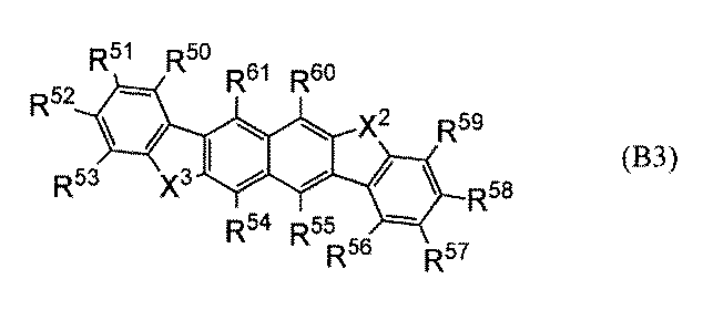

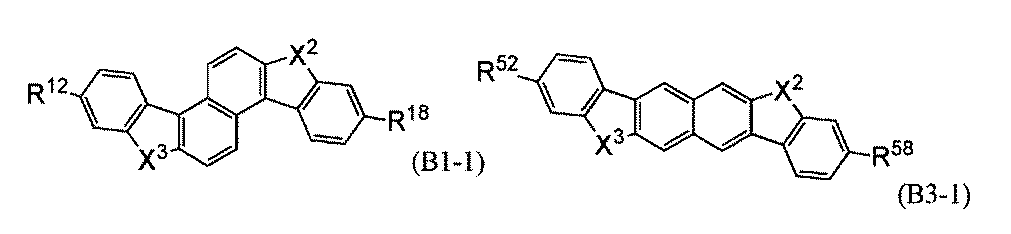

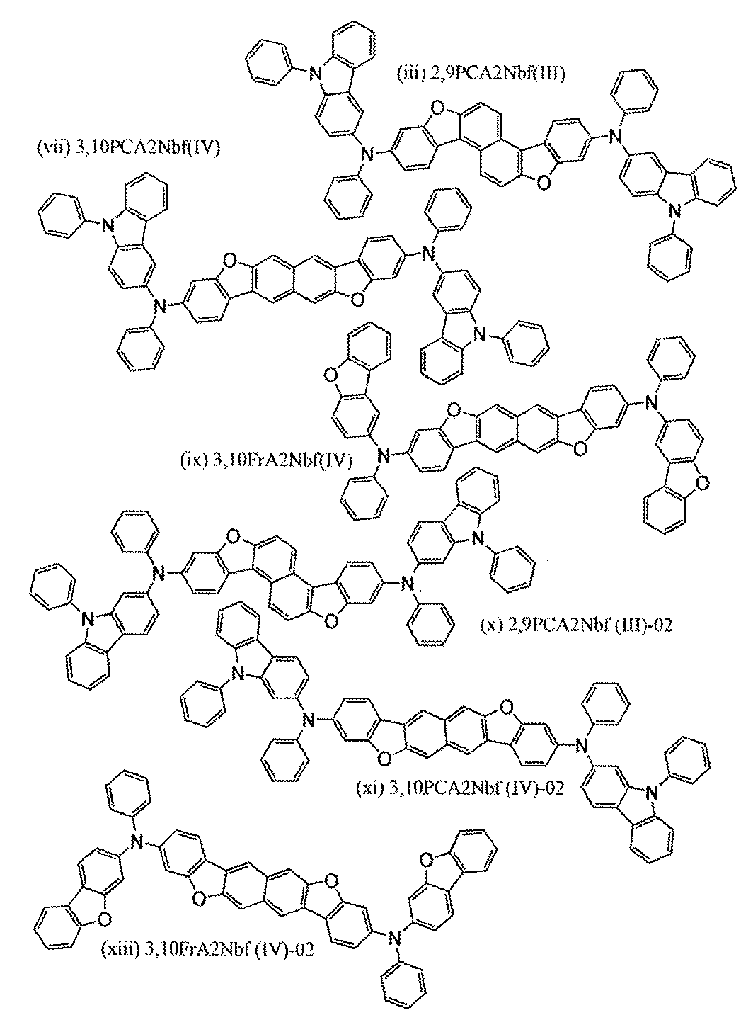
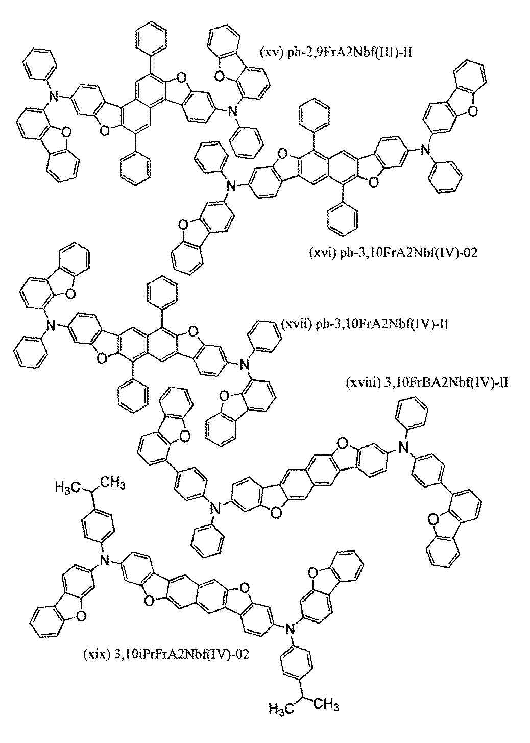

本発明の一態様の有機化合物は、下記一般式(G1)で表される有機化合物である。


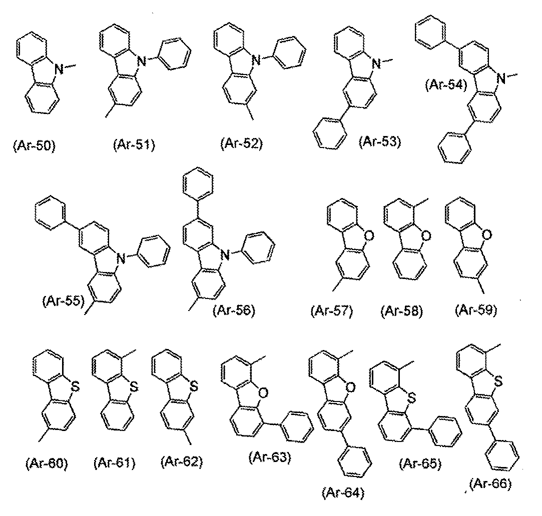


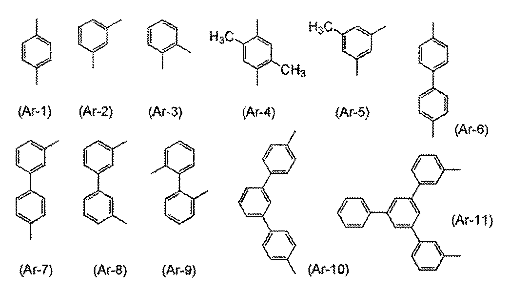

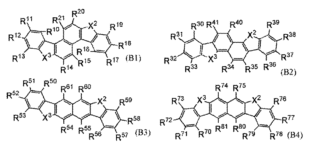
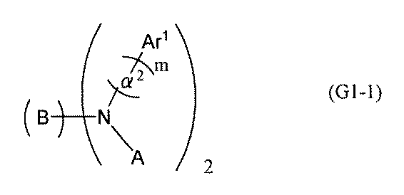


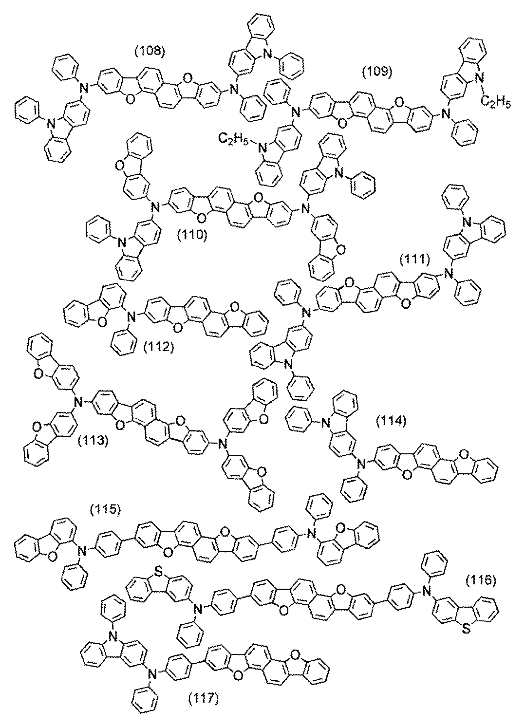

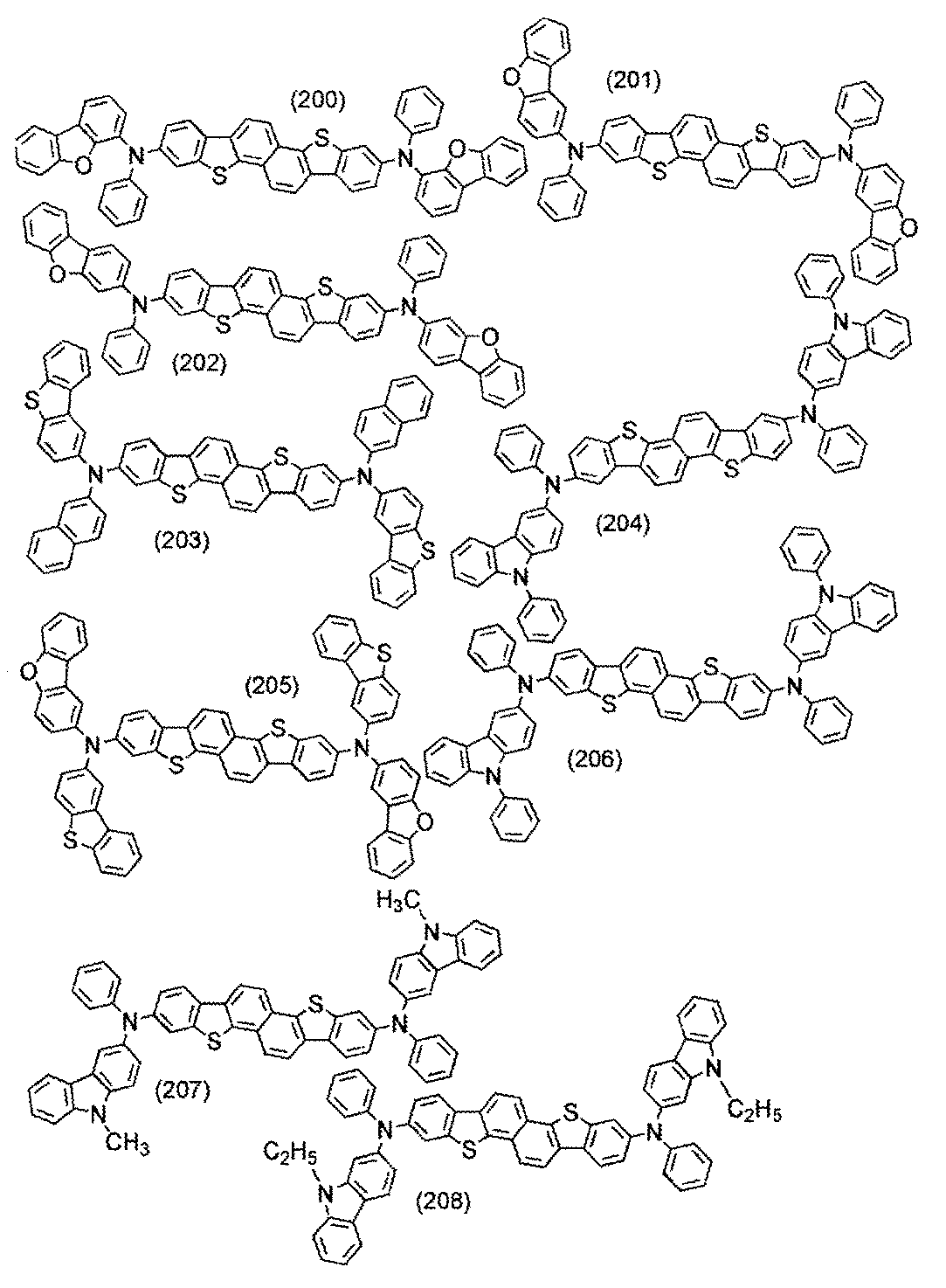

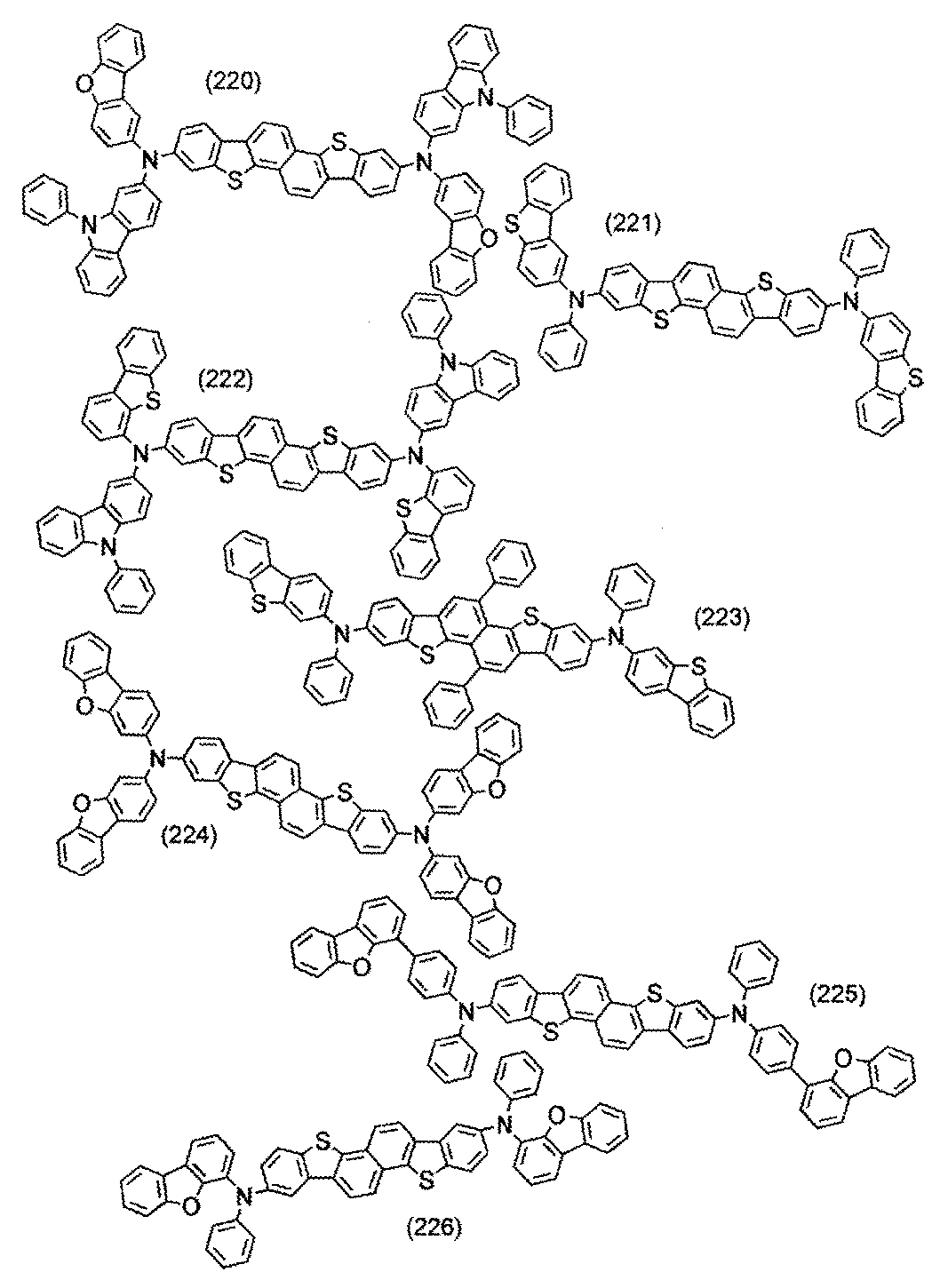
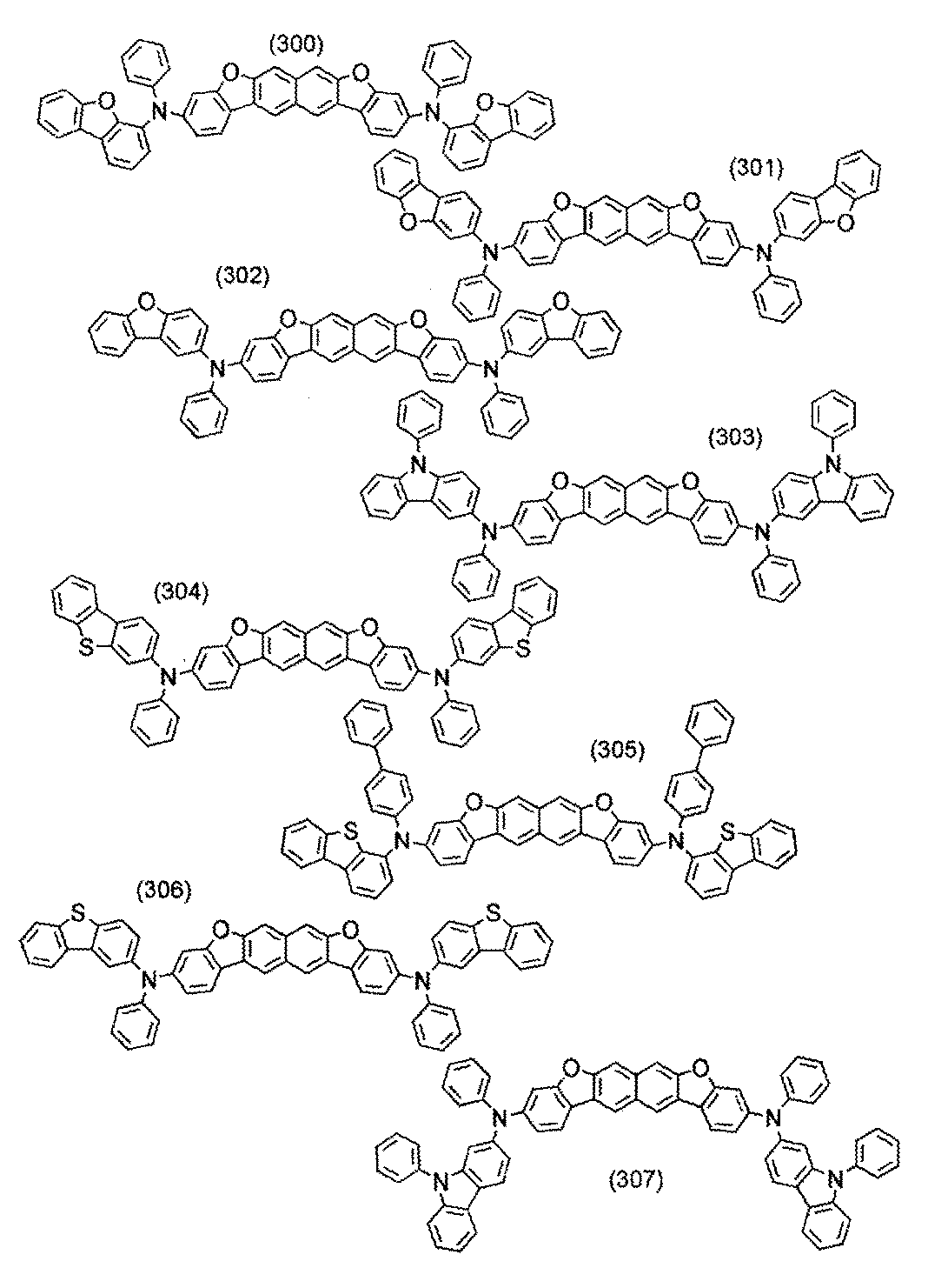
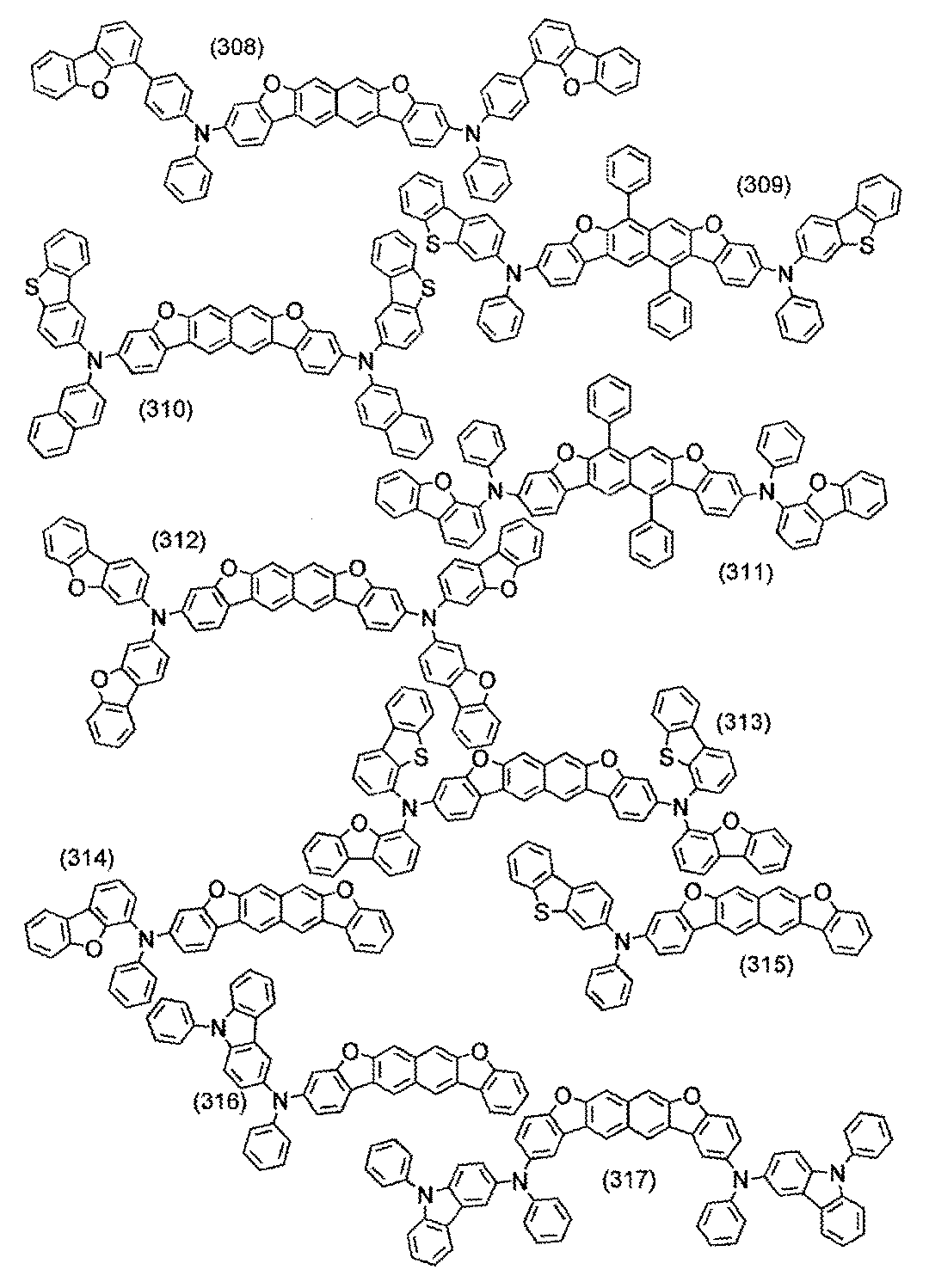


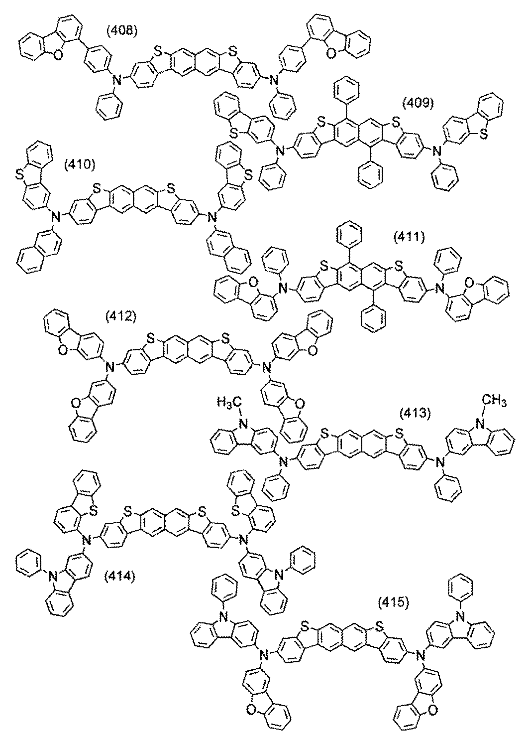
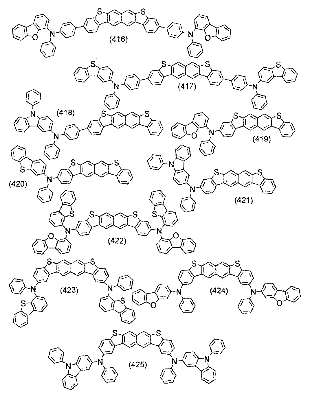
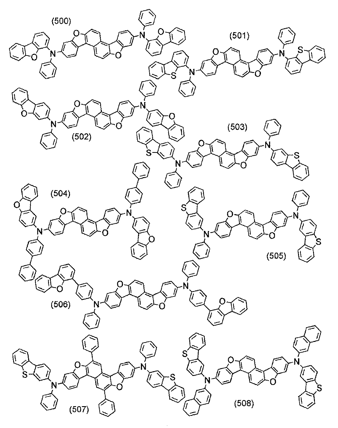

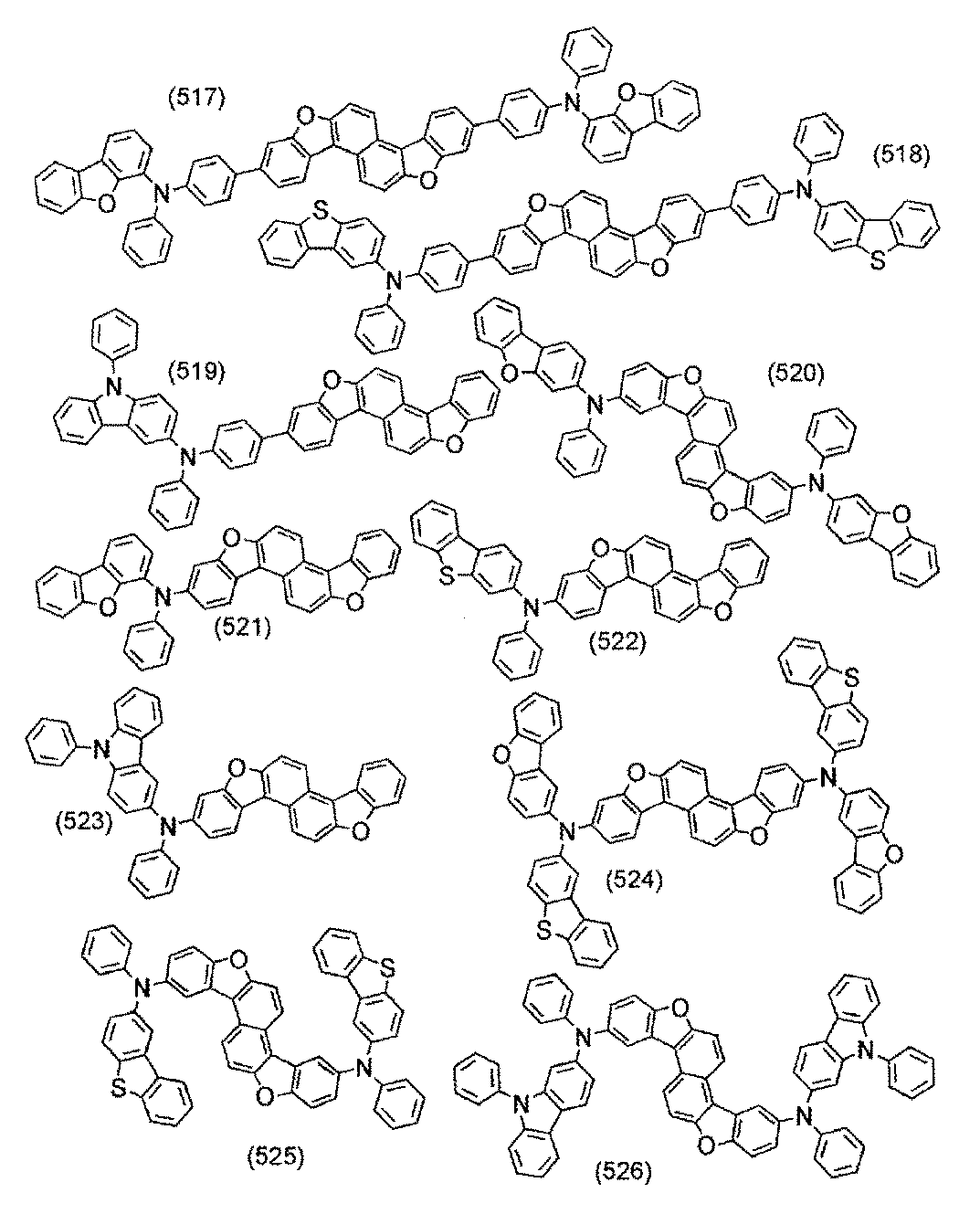
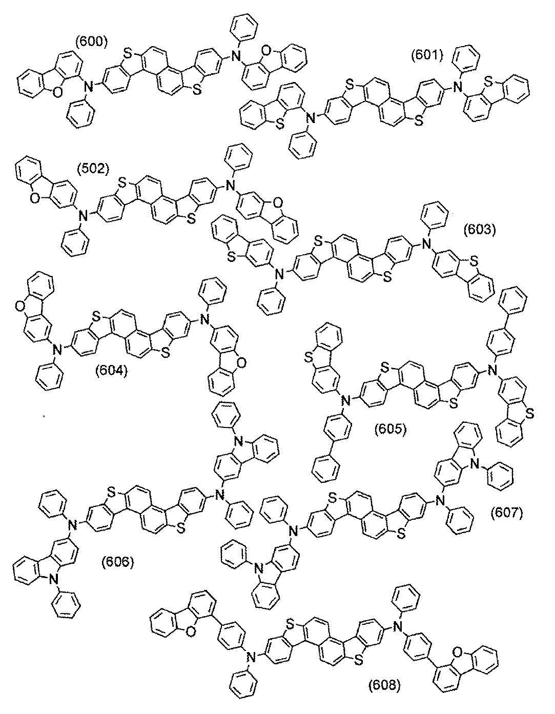

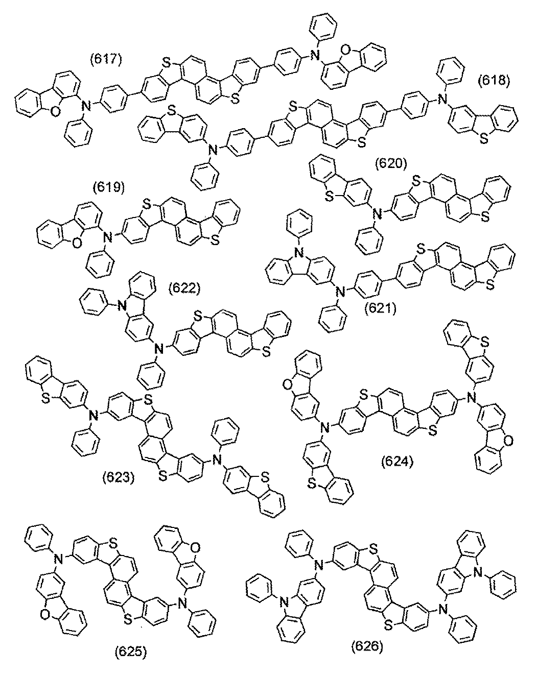
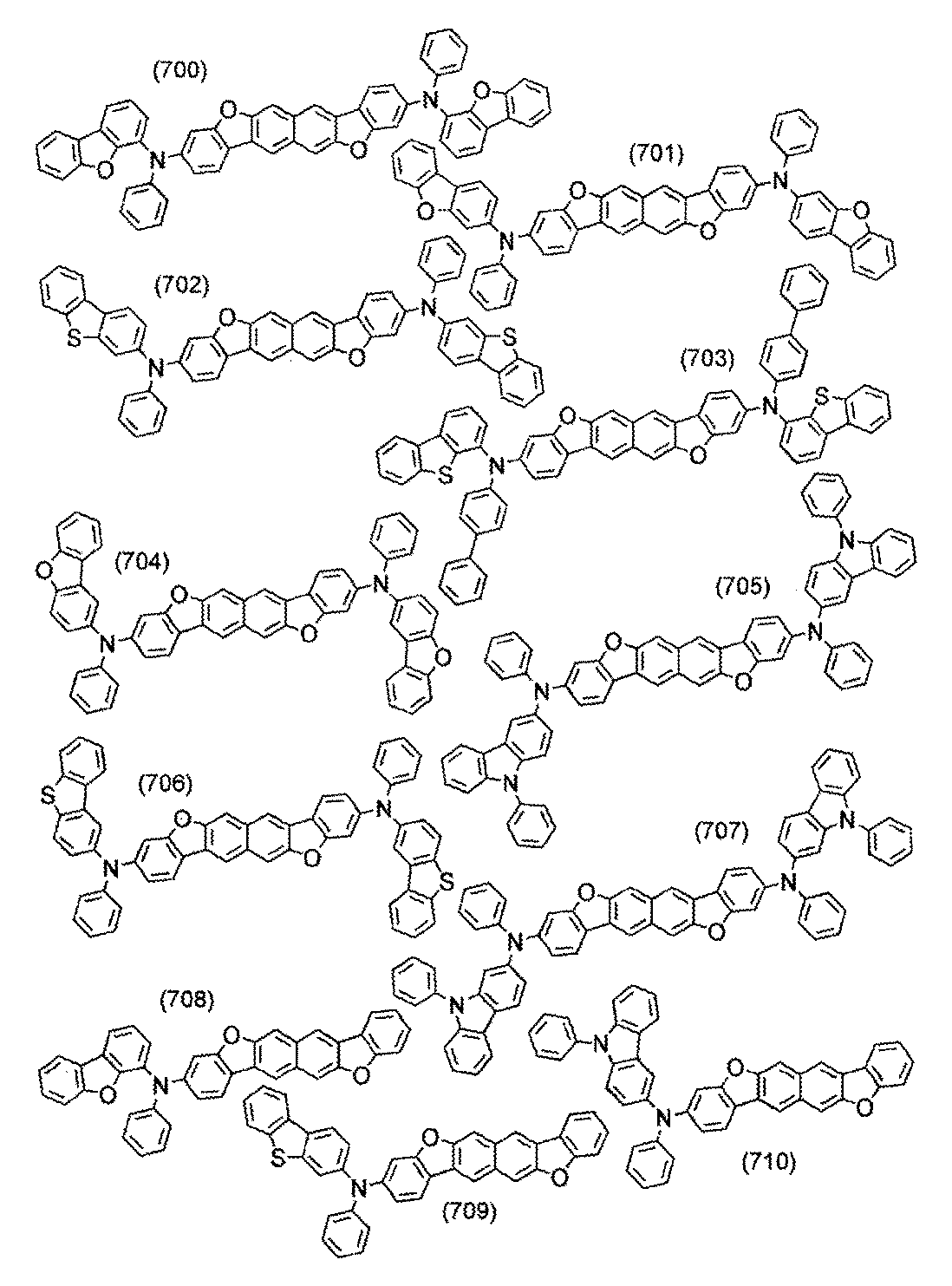
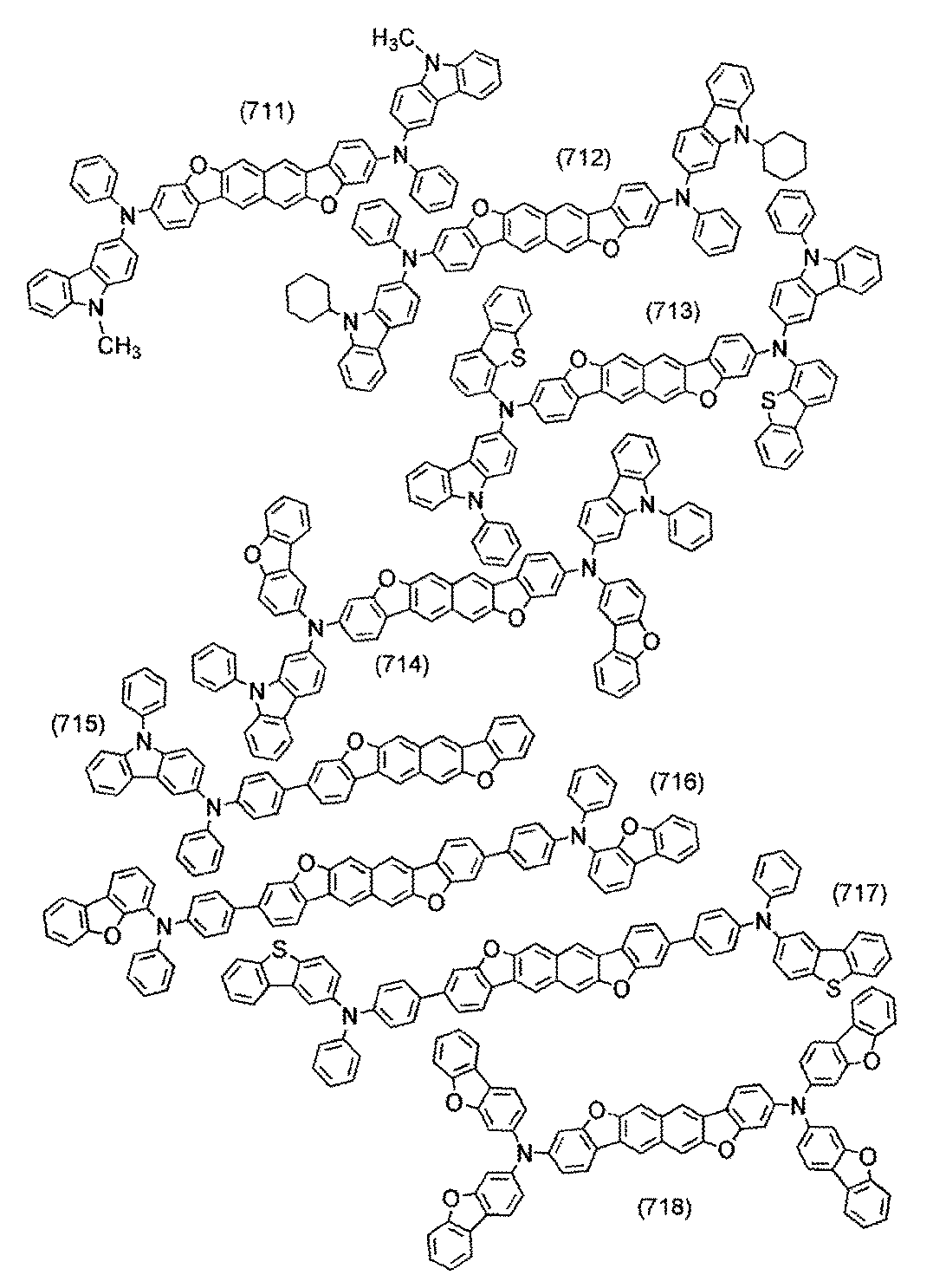

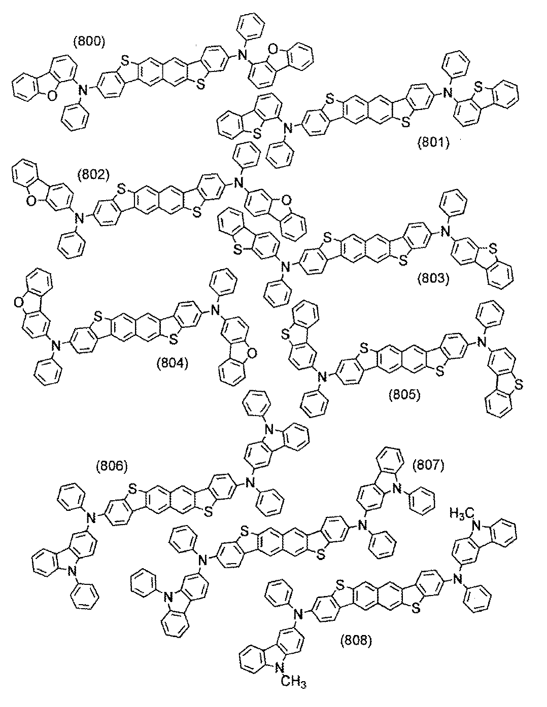


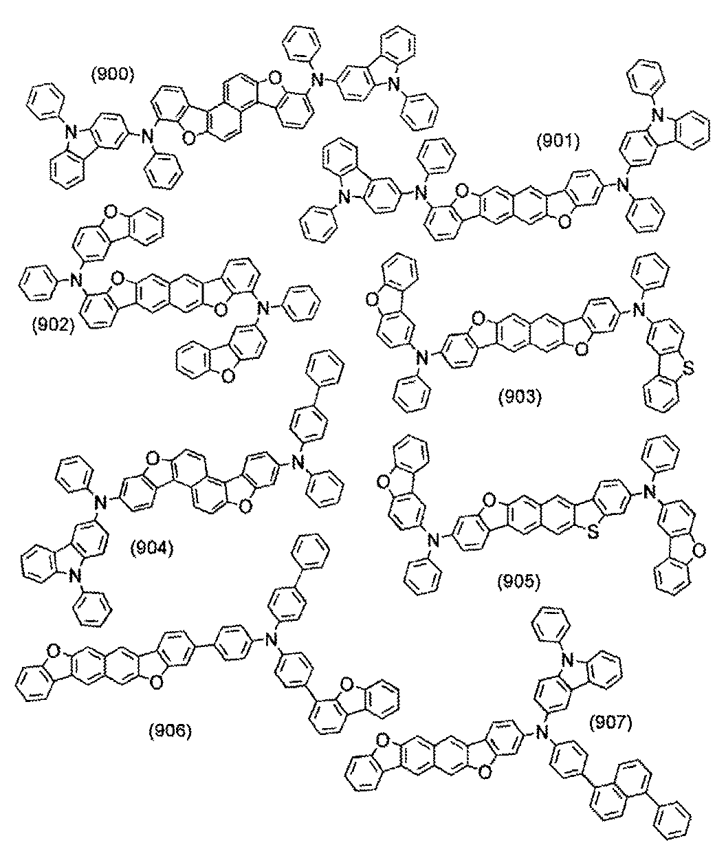


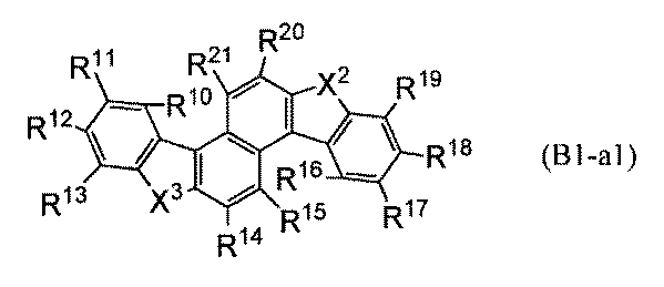

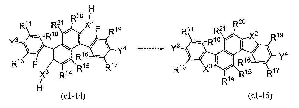
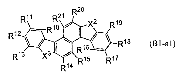


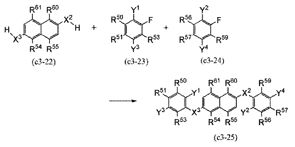

本発明の一態様である発光素子の例について図1(A)を用いて以下、詳細に説明する。


本実施の形態では、実施の形態1に記載の発光素子を用いた発光装置について説明する。
本発明の一態様である照明装置を図8を参照しながら説明する。図8(B)は照明装置の上面図、図8(A)は図8(B)におけるe−f断面図である。
本発明の一態様である電子機器の例について説明する。電子機器として、例えば、テレビジョン装置(テレビ、またはテレビジョン受信機ともいう)、コンピュータ用などのモニタ、デジタルカメラ、デジタルビデオカメラ、デジタルフォトフレーム、携帯電話機(携帯電話、携帯電話装置ともいう)、携帯型ゲーム機、携帯情報端末、音響再生装置、パチンコ機などの大型ゲーム機などが挙げられる。これらの電子機器の具体例を以下に示す。
本合成例では、実施の形態1で構造式(704)として示した3,10−ビス[N−(ジベンゾフラン−2−イル)−N−フェニルアミノ]ナフト[2,3−b;6,7−b’]ビスベンゾフラン(略称:3,10FrA2Nbf(IV))の合成方法について詳細に説明する。3,10FrA2Nbf(IV)の構造式を以下に示す。
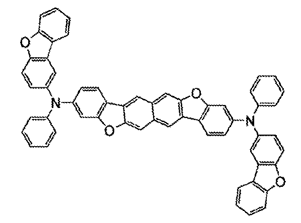
500mL三口フラスコに11g(24mmol)の3,7−ジヨード−2,6−ジメトキシナフタレンと、14g(78mmol)の4−クロロ−2−フルオロフェニルボロン酸と、22g(0.16mol)の炭酸カリウムと、0.74g(2.4mmol)のトリス(2−メチルフェニル)ホスフィンを入れた。この混合物に、120mLのトルエンを加えた。この混合物を減圧しながら攪拌することで脱気した。この混合物に0.11g(0.49mmol)の酢酸パラジウム(II)を加え、窒素気流下、110℃で50.5時間攪拌した。

1H NMR(CDCl3,300MHz):δ=3.88(s,6H),7.18−7.24(m,6H),7.37(t,J1=7.2Hz,2H),7.65(s,2H).
200mL三口フラスコに5.7g(13mmol)の3,7−ビス(4−クロロ−2−フルオロフェニル)−2,6−ジメトキシナフタレンを入れ、フラスコ内を窒素置換した。このフラスコに32mLのジクロロメタンを加えた。この溶液に28mL(28mmol)の三臭化ホウ素(約1.0mol/Lジクロロメタン溶液)と20mLのジクロロメタンを滴下した。滴下終了後、この溶液を室温で攪拌した。

1H NMR(DMSO−d6,300MHz):δ=7.20(s,2H),7.37(dd,J1=8.4Hz,J2=1.8Hz,2H),7.46−7.52(m,4H),7.59(s,2H),9.71(s,2H).
200mLの三口フラスコに5.4g(13mmol)の3,7−ビス(4−クロロ−2−フルオロフェニル)−2,6−ジヒドロキシナフタレンと7.1g(52mmol)の炭酸カリウムを入れた。この混合物に、N−メチル−2−ピロリドン130mLを加え、この混合物を減圧しながら攪拌することで脱気した。脱気後、この混合物を、窒素気流下、120℃で7時間攪拌した。撹拌後、この混合物に水を加え、析出した固体を濾取した。この固体を水、エタノールで洗浄した。得られた固体にエタノールを加え、加熱撹拌後、濾過し固体を得た。得られた固体に酢酸エチルを加え、加熱撹拌後、濾過して淡黄色固体を4.5g、収率92%で得た。ステップ3の合成スキームを以下に示す。

1H NMR(1,1,2,2−Tetrachloroethane−D2,300MHz):δ=7.44(dd,J1=8.1Hz,J2=1.5Hz,2H),7.65(d,J1=1.8Hz,2H),8.05(d,J1=8.4Hz,2H),8.14(s,2H),8.52(s,2H).
200mL三口フラスコに1.2g(3.0mmol)の3,10−ジクロロナフト[2,3−b;6,7−b’]ビスベンゾフランと、2.4g(9.1mmol)の2−アニリノジベンゾフランと、0.11g(0.30mmol)のジ(1−アダマンチル)−n−ブチルホスフィンと、1.8g(18mmol)のナトリウム tert−ブトキシドを入れた。この混合物に、30mLのキシレンを加えた。この混合物を減圧しながら攪拌することで脱気した。この混合物に35mg(61μmol)のビス(ジベンジリデンアセトン)パラジウム(0)を加え、窒素気流下、150℃で13時間攪拌した。
昇華精製後、黄色固体を0.93g、回収率87%で得た。ステップ4の合成スキームを以下に示す。
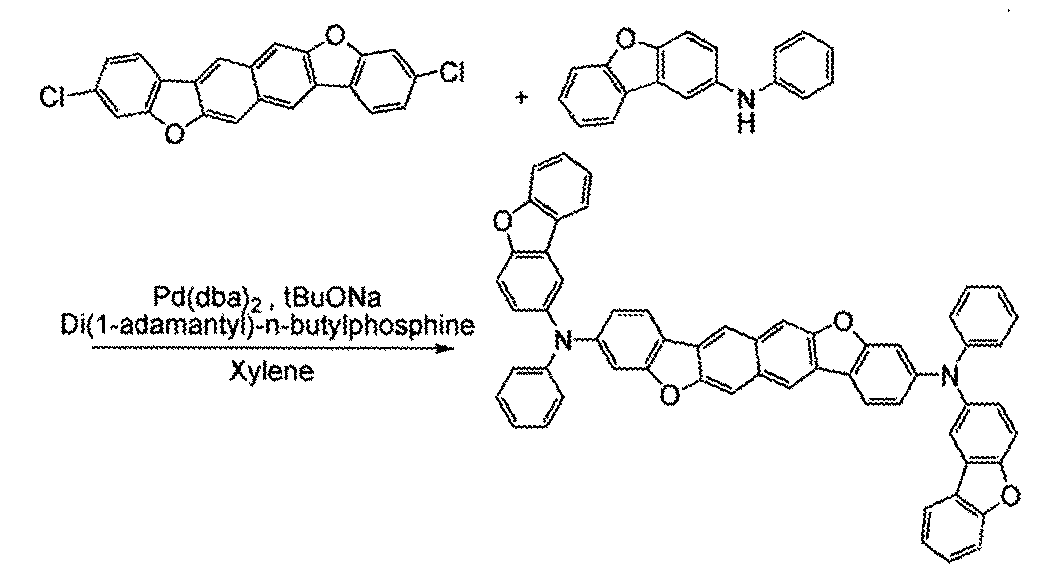
1H NMR(1,1,2,2−Tetrachloroethane−D2,300MHz):δ=7.08−7.13(m,4H),7.22−7.24(m,6H),7.31−7.36(m,8H),7.49(t,J1=7.2Hz,2H),7.56−7.62(m,4H),7.83−7.90(m,6H),7.98(s,2H),8.35(s,2H).
また、m/z=565付近のプロダクトイオンは、3,10FrA2Nbf(IV)におけるN−(ジベンゾフラン−2−イル)−N−フェニルアミノ基が離脱した状態のカチオンと推定され、3,10FrA2Nbf(IV)が、N−(ジベンゾフラン−2−イル)−N−フェニルアミノ基を含んでいることを示唆するものである。
本合成例では、実施の形態1で構造式(509)として示した2,9−ビス[N−(9−フェニル−9H−カルバゾール−3−イル)−N−フェニルアミノ]ナフト[2,1−b;6,5−b’]ビスベンゾフラン(略称:2,9PCA2Nbf(III))の合成方法について詳細に説明する。2,9PCA2Nbf(III)の構造式を以下に示す。

500mL三口フラスコに6.2g(19mmol)の1,5−ジブロモ−2,6−ジヒドロキシナフタレンと、7.5g(43mmol)の5−クロロ−2−フルオロフェニルボロン酸と、25g(78mmol)の炭酸セシウムと、0.80g(1.9mmol)の2−ジシクロヘキシルホスフィノ−2’−6’−ジメトキシ−1,1’−ビフェニル(略称:Sphos)を入れた。この混合物に、195mLのトルエンを加えた。この混合物を減圧しながら攪拌することで脱気した。この混合物に0.17g(0.78mmol)の酢酸パラジウム(II)を加え、窒素気流下、110℃で7時間攪拌した。撹拌後、混合物にトルエンを加え、セライト(和光純薬工業株式会社、カタログ番号:531−16855)を通して吸引ろ過し、濾液を得た。得られた濾液を濃縮し固体を得た。得られた固体をシリカゲルカラムクロマトグラフィー(中性シリカゲル、展開溶媒:トルエン)で精製し、固体を得た。
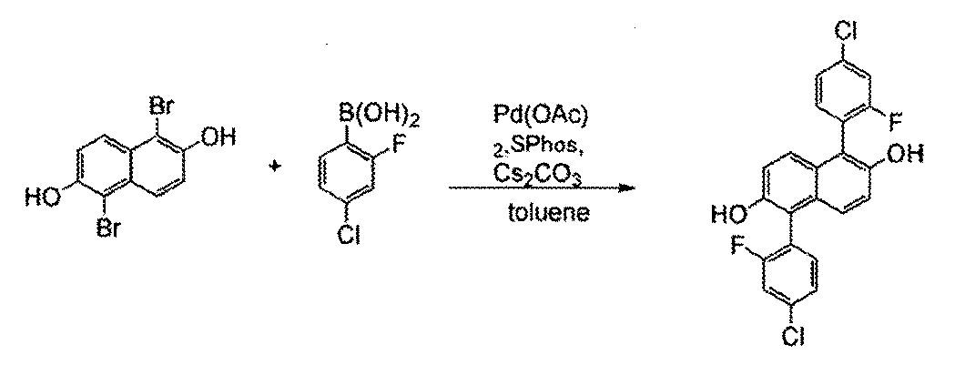
1H NMR(CDCl3,300MHz):δ=4.78(s,2H),7.15(d,J1=9.3Hz,2H),7.30−7.38(m,8H).
200mLの三口フラスコに2.8g(6.8mmol)の1,5−ビス(4−クロロ−2−フルオロフェニル)−2,7−ジヒドロキシナフタレンと3.7g(27mmol)の炭酸カリウムを入れた。この混合物に、N−メチル−2−ピロリドン70mLを加え、この混合物を減圧しながら攪拌することで脱気した。脱気後、この混合物を、窒素気流下、120℃で7.5時間攪拌した。撹拌後、この混合物に水を加え、析出した固体を濾取した。この固体を水、エタノールで洗浄した。得られた固体にエタノールを加え、加熱撹拌後、固体を回収した。得られた固体にトルエンを加え、加熱撹拌後、析出した固体を回収し、白色固体を2.3g、収率91%で得た。ステップ2の合成スキームを以下に示す。

1H NMR(1,1,2,2−Tetrachloroethane−D2,300MHz):δ=7.56(dd,J1=8.1Hz,J2=1.5Hz,2H),7.81(d,J1=1.8Hz,2H),8.06(d,J1=8.7Hz,2H),8.40(d,J1=8.4Hz,2H),8.73(d,J1=8.7Hz,2H).
200mL三口フラスコに1.2g(3.1mmol)の2,9−ジクロロナフト[2,1−b;6,5−b’]ビスベンゾフランと、3.1g(9.2mmol)の3−アニリノ−9−フェニル−9H−カルバゾールと、0.11g(0.31mmol)のジ(1−アダマンチル)−n−ブチルホスフィンと、1.8g(18mmol)のナトリウム tert−ブトキシドを入れた。この混合物に、30mLのキシレンを加えた。この混合物を減圧しながら攪拌することで脱気した。この混合物に35mg(62μmol)のビス(ジベンジリデンアセトン)パラジウム(0)を加え、窒素気流下、150℃で11時間攪拌した。
昇華精製後、黄色固体を0.96g、回収率80%で得た。ステップ3の合成スキームを以下に示す。

1H NMR(DMSO−d6,300MHz):δ=7.08(t,J1=7.2Hz,2H),7.15−7.27(m,8H),7.30−7.47(m,14H),7.53−7.58(m,2H),7.67−7.73(m,8H),8.05(d,J1=9.3Hz,2H),8.18(d,J1=2.1Hz,2H),8.21(d,J1=7.2Hz,2H),8.50(d,J1=8.7Hz,2H),8.71(d,J1=8.7Hz,2H).
本合成例では、実施の形態1で構造式(705)として示した3,10−ビス[N−(9−フェニル−9H−カルバゾール−3−イル)−N−フェニルアミノ]ナフト[2,3−b;6,7−b’]ビスベンゾフラン(略称:3,10PCA2Nbf(IV))の合成方法について詳細に説明する。3,10PCA2Nbf(IV)の構造式を以下に示す。

実施例1における合成例1のステップ1と同様に合成した。
実施例1における合成例1のステップ2と同様に合成した。
実施例1における合成例1のステップ3と同様に合成した。
200mL三口フラスコに1.2g(3.1mmol)の3,10−ジクロロナフト[2,3−b;6,7−b’]ビスベンゾフランと、3.1g(9.2mmol)の3−アニリノ−9−フェニル−9H−カルバゾールと、0.11g(0.31mmol)のジ(1−アダマンチル)−n−ブチルホスフィンと、1.8g(18mmol)のナトリウム tert−ブトキシドを入れた。この混合物に、30mLのキシレンを加えた。この混合物を減圧しながら攪拌することで脱気した。この混合物に35mg(62μmol)のビス(ジベンジリデンアセトン)パラジウム(0)を加え、窒素気流下、150℃で6時間攪拌した。

1H NMR(DMSO−d6,300MHz):δ=7.00−7.11(m,6H),7.20−7.25(m,6H),7.30−7.45(m,12H),7.54(t,J1=6.6Hz,2H),7.61−7.71(m,8H),8.00(d,J1=8.7Hz,2H),8.08−8.16(m,6H),8.52(s,2H).
また、m/z=332付近のプロダクトイオンは、3,10PCA2Nbf(IV)における3−[N−(9−フェニル−9H−カルバゾール−3−イル)−N−フェニルアミノ]ナフト[2,1−b;6,5−b’]ビスベンゾフラニル基が離脱した状態のカチオンと推定され、3,10PCA2Nbf(IV)が、3−[N−(9−フェニル−9H−カルバゾール−3−イル)−N−フェニルアミノ]ナフト[2,1−b;6,5−b’]ビスベンゾフラニル基を含んでいることを示唆するものである。

まず、ガラス基板上に、酸化珪素を含むインジウム錫酸化物(ITSO)をスパッタリング法にて成膜し、陽極101を形成した。なお、その膜厚は70nmとし、電極面積は4mm2(2mm×2mm)とした。
比較発光素子1は、発光素子1における発光層113に用いた2,9PCA2Nbf(III)を上記構造式(v)で表される2,9−ビス(ジフェニルアミノ)ナフト[2,1−b;6,5−b’]ビスベンゾフラン(略称:2,9DPhA2Nbf(III))に変えて発光層113を形成し、また、cgDBCzPAを膜厚10nmとなるよう蒸着した後、BPhenを膜厚15nmとなるように蒸着して電子輸送層114を形成することにより作製した。比較発光素子1で用いた2,9DPhA2Nbf(III)と、発光素子1で用いた2,9PCA2Nbf(III)は、主骨格であるナフトビスベンゾフランの構造は同一であるが、結合するアミンの構造が異なる物質である。
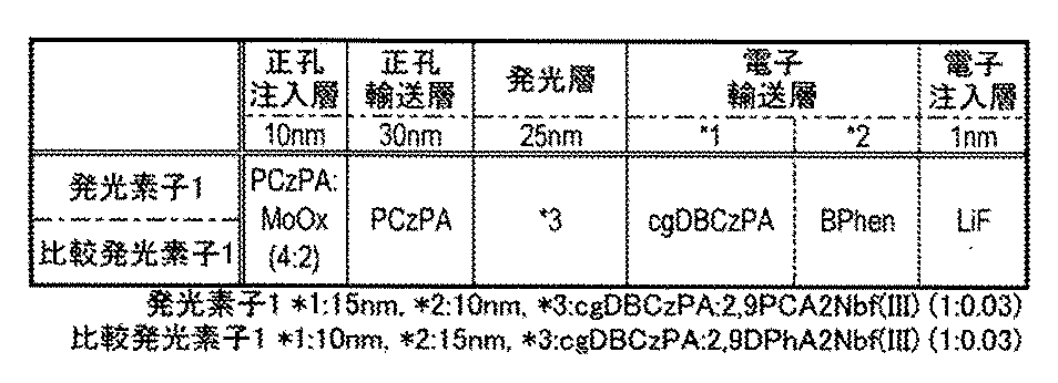


まず、ガラス基板上に、酸化珪素を含むインジウム錫酸化物(ITSO)をスパッタリング法にて成膜し、陽極101を形成した。なお、その膜厚は70nmとし、電極面積は4mm2(2mm×2mm)とした。
比較発光素子2は、発光素子2における発光層113に用いた2,9PCA2Nbf(III)を上記構造式(v)で表される2,9−ビス(ジフェニルアミノ)ナフト[2,1−b;6,5−b’]ビスベンゾフラン(略称:2,9DPhA2Nbf(III))に変えて発光層113を形成し、また、cgDBCzPAを膜厚10nmとなるよう蒸着した後、BPhenを膜厚15nmとなるように蒸着して電子輸送層114を形成することにより作製した。比較発光素子2で用いた2,9DPhA2Nbf(III)と、発光素子2で用いた2,9PCA2Nbf(III)は、主骨格であるナフトビスベンゾフランの構造は同一であるが、結合するアミンの構造が異なる物質である。
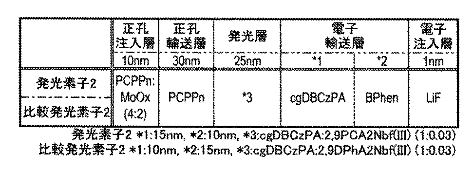

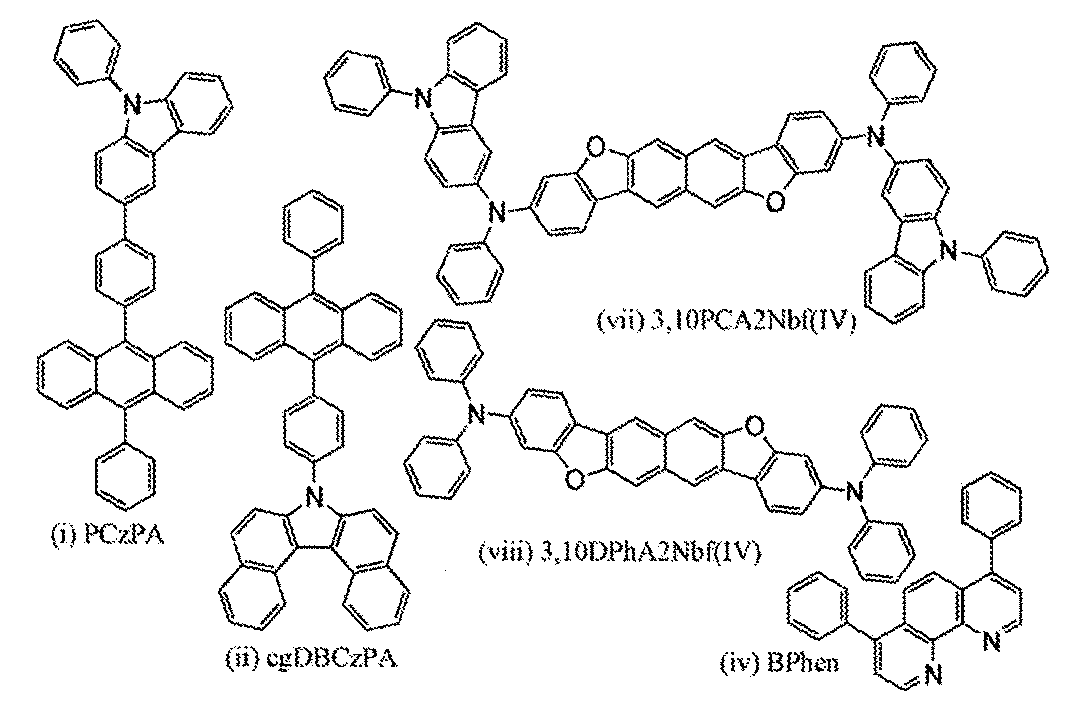
まず、ガラス基板上に、酸化珪素を含むインジウム錫酸化物(ITSO)をスパッタリング法にて成膜し、陽極101を形成した。なお、その膜厚は70nmとし、電極面積は4mm2(2mm×2mm)とした。
比較発光素子3は、発光素子3における発光層113に用いた3,10PCA2Nbf(IV)を上記構造式(viii)で表される3,10−ビス(ジフェニルアミノ)ナフト[2,3−b;6,7−b’]ビスベンゾフラン(略称:3,10DPhA2Nbf(IV))に変えて発光層113を形成することにより作製した。比較発光素子3で用いた3,10DPhA2Nbf(IV)と、発光素子3で用いた3,10PCA2Nbf(IV)は、主骨格であるナフトビスベンゾフランの構造は同一であるが、結合するアミンの構造が異なる物質である。


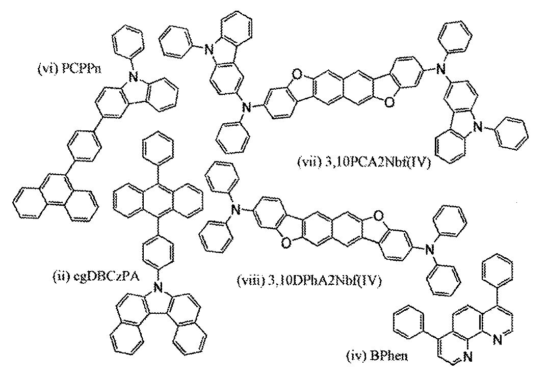
まず、ガラス基板上に、酸化珪素を含むインジウム錫酸化物(ITSO)をスパッタリング法にて成膜し、陽極101を形成した。なお、その膜厚は70nmとし、電極面積は4mm2(2mm×2mm)とした。
比較発光素子4は、発光素子4における発光層113に用いた3,10PCA2Nbf(IV)を上記構造式(viii)で表される3,10−ビス(ジフェニルアミノ)ナフト[2,3−b;6,7−b’]ビスベンゾフラン(略称:3,10DPhA2Nbf(IV))に変えて発光層113を形成することにより作製した。比較発光素子4で用いた3,10DPhA2Nbf(IV)と、発光素子4で用いた3,10PCA2Nbf(IV)は、主骨格であるナフトビスベンゾフランの構造は同一であるが、結合するアミンの構造が異なる物質である。


まず、ガラス基板上に、酸化珪素を含むインジウム錫酸化物(ITSO)をスパッタリング法にて成膜し、陽極101を形成した。なお、その膜厚は70nmとし、電極面積は4mm2(2mm×2mm)とした。
比較発光素子5は、発光素子5における発光層113に用いた3,10FrA2Nbf(IV)を上記構造式(viii)で表される3,10−ビス(ジフェニルアミノ)ナフト[2,3−b;6,7−b’]ビスベンゾフラン(略称:3,10DPhA2Nbf(IV))に変えて発光層113を形成することにより作製した。比較発光素子5で用いた3,10DPhA2Nbf(IV)と、発光素子5で用いた3,10FrA2Nbf(IV)は、主骨格であるナフトビスベンゾフランの構造は同一であるが、結合するアミンの構造が異なる物質である。
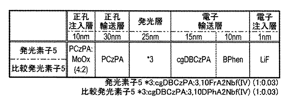

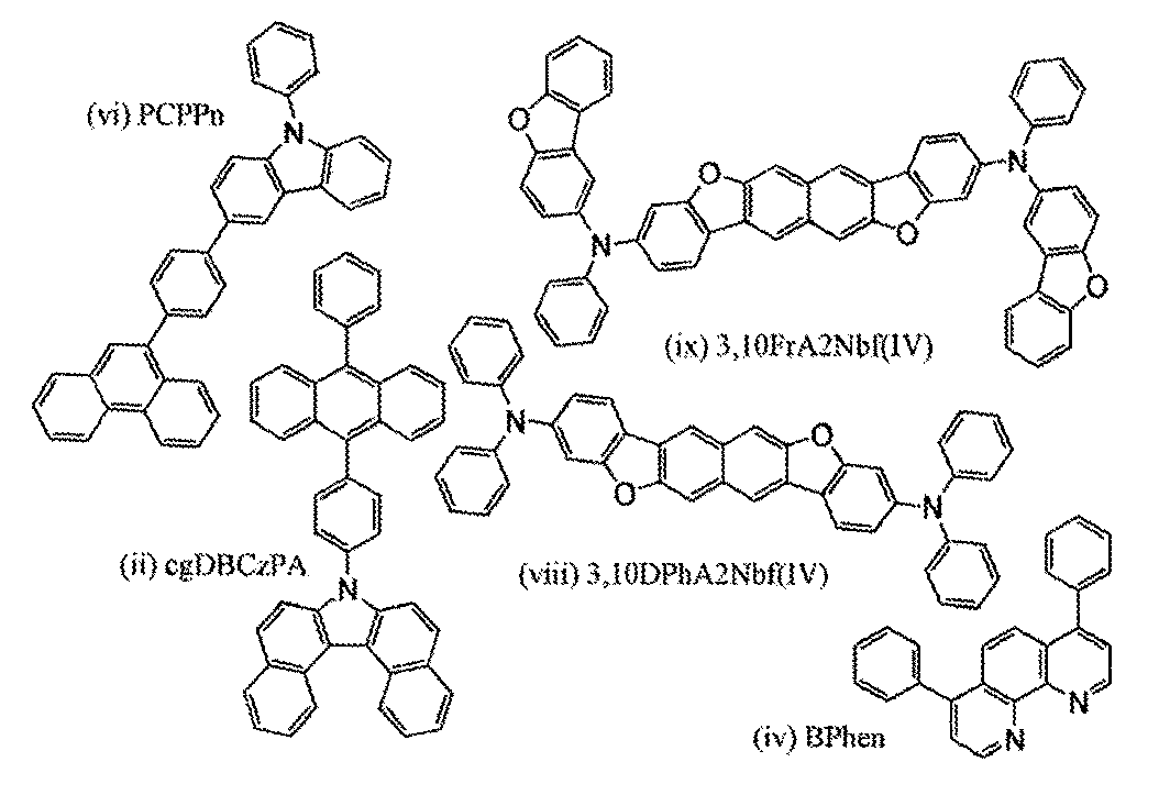
まず、ガラス基板上に、酸化珪素を含むインジウム錫酸化物(ITSO)をスパッタリング法にて成膜し、陽極101を形成した。なお、その膜厚は70nmとし、電極面積は4mm2(2mm×2mm)とした。
比較発光素子6は、発光素子6における発光層113に用いた3,10FrA2Nbf(IV)を上記構造式(viii)で表される3,10−ビス(ジフェニルアミノ)ナフト[2,3−b;6,7−b’]ビスベンゾフラン(略称:3,10DPhA2Nbf(IV))に変えて発光層113を形成することにより作製した。比較発光素子6で用いた3,10DPhA2Nbf(IV)と、発光素子6で用いた3,10FrA2Nbf(IV)は、主骨格であるナフトビスベンゾフランの構造は同一であるが、結合するアミンの構造が異なる物質である。
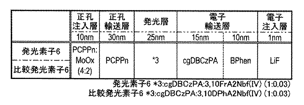

本合成例では、実施の形態1において構造式(510)として示した、2,9−ビス[N−(9−フェニル−9H−カルバゾール−3−イル)−N−フェニルアミノ]ナフト[2,1−b;6,5−b’]ビスベンゾフラン(略称:2,9PCA2Nbf(III)−02)の合成方法について詳細に説明する。2,9PCA2Nbf(III)−02の構造式を以下に示す。

実施例2における合成例2のステップ1と同様に合成した。
実施例2における合成例2のステップ2と同様に合成した。
200mL三口フラスコに0.90g(2.4mmol)の2,9−ジクロロナフト[2,1−b;6,5−b’]ビスベンゾフランと、2.0g(6.0mmol)の2−アニリノ−9−フェニル−9H−カルバゾールと、86mg(0.24mmol)のジ(1−アダマンチル)−n−ブチルホスフィンと、1.4g(14mmol)のナトリウム tert−ブトキシドを入れた。この混合物に、25mLのキシレンを加えた。この混合物を減圧しながら攪拌することで脱気した。この混合物に28mg(48μmol)のビス(ジベンジリデンアセトン)パラジウム(0)を加え、窒素気流下、150℃で11時間攪拌した。撹拌後、この混合物にトルエンを加え、フロリジール、セライト、アルミナを通して吸引ろ過し、濾液を得た。得られた濾液を濃縮し固体を得た。この固体をシリカゲルカラムクロマトグラフィー(展開溶媒:トルエン)で精製し、固体を得た。得られた固体をトルエンで3回再結晶し、黄色固体を0.76g、収率33%で得た。

1H NMR(CD2Cl2,300MHz):δ=7.07(tt,J1=7.5Hz,J2=1.5Hz,2H),7.13(dd,J1=8.1Hz,J2=1.8Hz,2H),7.19−7.33(m,14H),7.35−7.40(m,8H),7.51−7.53(m,8H),7.91(d,J1=8.7Hz,2H),8.07−8.11(m,4H),8.26(d,J1=8.7Hz,2H),8.60(d,J1=8.7Hz,2H).
なお、m/z=640付近のプロダクトイオンは、2,9PCA2Nbf(III)−02におけるN−(9−フェニル−9H−カルバゾール−2−イル)−N−フェニルアミノ基が離脱した状態のカチオンと推定され、2,9PCA2Nbf(III)−02が、N−(9−フェニル−9H−カルバゾール−2−イル)−N−フェニルアミノ基を含んでいることを示唆するものである。
また、m/z=333付近のプロダクトイオンは、2,9PCA2Nbf(III)−02における2−[N−(9−フェニル−9H−カルバゾール−2−イル)−N−フェニルアミノ]ナフト[2,1−b;6,5−b’]ビスベンゾフラニル基が離脱した状態のカチオンと推定され、2,9PCA2Nbf(III)−02が、2−[N−(9−フェニル−9H−カルバゾール−2−イル)−N−フェニルアミノ]ナフト[2,1−b;6,5−b’]ビスベンゾフラニル基を含んでいることを示唆するものである。
本合成例では、実施の形態1において構造式(701)として示した、3,10−ビス[N−(ジベンゾフラン−3−イル)−N−フェニルアミノ]ナフト[2,3−b;6,7−b’]ビスベンゾフラン(略称:3,10FrA2Nbf(IV)−02)の合成方法について詳しく説明する。3,10FrA2Nbf(IV)−02の構造式を以下に示す。

実施例1における合成例1のステップ1と同様に合成した。
実施例1における合成例1のステップ2と同様に合成した。
実施例1における合成例1のステップ3と同様に合成した。
200mL三口フラスコに1.2g(3.0mmol)の3,10−ジクロロナフト[2,3−b;6,7−b’]ビスベンゾフランと、2.0g(7.7mmol)のN−(ジベンゾフラン−3−イル)−N−フェニルアミン、0.11g(0.30mmol)のジ(1−アダマンチル)−n−ブチルホスフィン、1.8g(18mmol)のナトリウム tert−ブトキシドを入れた。この混合物に、30mLのキシレンを加えた。この混合物を減圧しながら攪拌することで脱気した。この混合物に35mg(61μmol)のビス(ジベンジリデンアセトン)パラジウム(0)を加え、窒素気流下、150℃で32時間攪拌した。

1H NMR(CD2Cl2,300MHz):δ=7.12−7.21(m,6H),7.23−7.26(m,4H),7.28(d,J1=2.1Hz,2H),7.32−7.40(m,8H),7.44(dd,J1=7.5Hz,J2=1.2Hz,2H),7.53(d,J1=7.8Hz,2H),7.88(d,J1=8.1Hz,2H),7.91−7.96(m,4H),8.01(s,2H),8.41(s,2H).
本合成例では、実施の形態1で構造式(707)として示した、3,10−ビス[N−(9−フェニル−9H−カルバゾール−2−イル)−N−フェニルアミノ]ナフト[2,3−b;6,7−b’]ビスベンゾフラン(略称:3,10PCA2Nbf(IV)−02)の合成方法について詳しく説明する。3,10PCA2Nbf(IV)−02の構造式を以下に示す。

実施例1における合成例1のステップ1と同様に合成した。
実施例1における合成例1のステップ2と同様に合成した。
実施例1における合成例1のステップ3と同様に合成した。
200mL三口フラスコに0.97g(2.6mmol)の3,10−ジクロロナフト[2,3−b;6,7−b’]ビスベンゾフランと、2.6g(7.7mmol)の2−アニリノ−9−フェニル−9H−カルバゾール、92mg(0.26mmol)のジ(1−アダマンチル)−n−ブチルホスフィン、1.5g(15mmol)のナトリウム tert−ブトキシドを入れた。この混合物に、26mLのキシレンを加えた。この混合物を減圧しながら攪拌することで脱気した。この混合物に30mg(51μmol)のビス(ジベンジリデンアセトン)パラジウム(0)を加え、窒素気流下、150℃で7時間攪拌した。撹拌後、この混合物にトルエンを加え、フロリジール、セライト、アルミナを通して吸引ろ過し、濾液を得た。得られた濾液を濃縮し固体を得た。この固体をシリカゲルカラムクロマトグラフィー(展開溶媒:トルエン)で精製し、固体を得た。得られた固体をトルエンで2回再結晶し、黄色固体を1.6g、収率62%で得た。
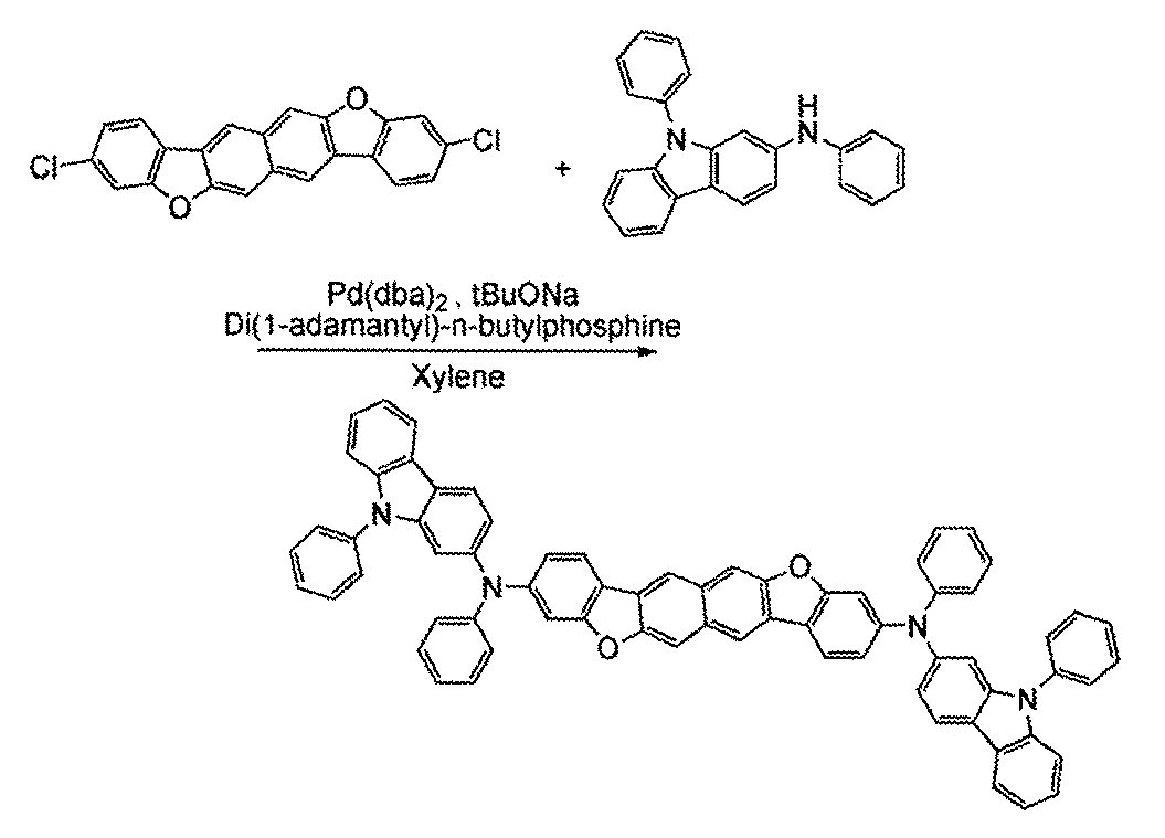
1H NMR(CD2Cl2,300MHz):δ=7.05−7.14(m,6H),7.19−7.24(m,8H),7.26−7.33(m,6H),7.36−7.41(m,6H),7.50−7.56(m,8H),7.88(d,J1=8.4Hz,2H),7.97(s,2H),8.08−8.12(m,4H),8.35(s,2H).
また、m/z=640付近のプロダクトイオンは、3,10PCA2Nbf(IV)−02におけるN−(9−フェニル−9H−カルバゾール−2−イル)−N−フェニルアミノ基が離脱した状態のカチオンと推定され、3,10PCA2Nbf(IV)−02が、N−(9−フェニル−9H−カルバゾール−2−イル)−N−フェニルアミノ基を含んでいることを示唆するものである。また、m/z=333付近のプロダクトイオンは、3,10PCA2Nbf(IV)−02における3−[N−(9−フェニル−9H−カルバゾール−2−イル)−N−フェニルアミノ]ナフト[2,3−b;6,7−b’]ビスベンゾフラニル基が離脱した状態のカチオンと推定され、3,10PCA2Nbf(IV)−02が、3−[N−(9−フェニル−9H−カルバゾール−2−イル)−N−フェニルアミノ]ナフト[2,3−b;6,7−b’]ビスベンゾフラニル基を含んでいることを示唆するものである。
本合成例では、3,10−ビス[N−(ジベンゾフラン−4−イル)−N−フェニルアミノ]−6,13−ジフェニルナフト[2,3−b;6,7−b’]ビスベンゾフラン(略称:ph−3,10FrA2Nbf(IV)−II)の合成方法について詳しく説明する。ph−3,10FrA2Nbf(IV)−IIの構造式を以下に示す。
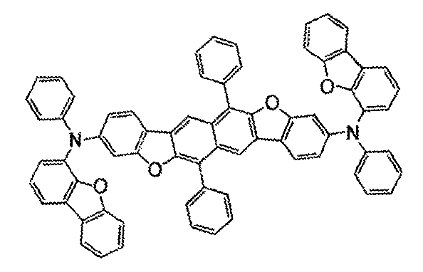
1L三口フラスコに9.5g(30mmol)の1,5−ジブロモ−2,6−ジヒドロキシナフタレン、8.0g(66mmol)のフェニルボロン酸、37g(120mmol)の炭酸セシウム、および1.2g(3.0mmol)のSPhosを入れた。この混合物に、300mLのトルエンを加えた。この混合物を減圧しながら攪拌することで脱気した。この混合物に0.27g(1.2mmol)の酢酸パラジウム(II)を加え、窒素気流下、110℃で7時間攪拌した。撹拌後、混合物にトルエンを加え、セライトを通して吸引ろ過し、濾液を得た。得られた濾液を濃縮し固体を得た。得られた固体をシリカゲルカラムクロマトグラフィー(中性シリカゲル、展開溶媒:トルエン)で精製し、黄色固体を4.3g(crude)を得た。ステップ1の合成スキームを以下に示す。

1H NMR(DMSO−d6,300MHz):δ=7.07(d,J1=9.3Hz,2H),7.19(d,J1=8.7Hz,2H),7.25−7.41(m,6H),7.45−7.51(m,4H),9.07(s,2H).
200mLの三口フラスコに4.3g(crude)の2,6−ジヒドロキシ−1,5−ジフェニルナフタレン、8.6g(0.42mol)の1−ブロモ−4−クロロ−2−フルオロベンゼン、および13g(41mmol)の炭酸セシウムを入れた。この混合物に、N−メチル−2−ピロリドン70mLを加え、この混合物を減圧しながら攪拌することで脱気した。脱気後、この混合物を、窒素気流下、120℃で13.5時間攪拌した。撹拌後、2.9g(14mmol)の1−ブロモ−4−クロロ−2−フルオロベンゼンを追加し、窒素気流下、120℃で13.5時間攪拌した。
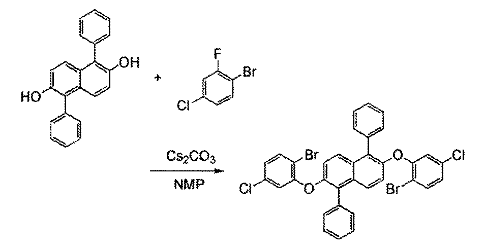
1H NMR(DMSO−d6,300MHz):δ=6.90(d,J1=1.8Hz,2H),7.06(dd,J1=8.1Hz,J2=2.4Hz,2H),7.28(d,J1=9.3Hz,2H),7.39−7.51(m,10H),7.56−7.61(m,4H).
200mLの三口フラスコに6.2g(9.0mmol)の2,6−ビス(2−ブロモ−4−クロロフェノキシ)−1,5−ジフェニルナフタレンと、0.47g(1.8mmol)のトリフェニルホスフィン、7.1g(22mmol)の炭酸セシウムを入れた。この混合物に、N−メチル−2−ピロリドン45mLを加え、この混合物を減圧しながら攪拌することで脱気した。脱気後、この混合物を、窒素気流下、120℃で15時間攪拌した。

1H NMR(1,1,2,2−Tetrachloroethane−D2,300MHz):δ=7.32(dd,J1=8.4Hz,J2=1.5Hz,2H),7.55(d,J1=1.5Hz,2H),7.65−7.76(m,10H),7.93(d,J1=8.1Hz,2H),8.47(s,2H).
200mL三口フラスコに1.4g(2.6mmol)の3,10−ジクロロ−6,13−ジフェニルナフト[2,3−b;6,7−b’]ビスベンゾフランと、1.7g(6.4mmol)のN−(ジベンゾフラン−4−イル)−N−フェニルアミン、92mg(0.26mmol)のジ(1−アダマンチル)−n−ブチルホスフィン、1.5g(15mmol)のナトリウム tert−ブトキシドを入れた。この混合物に、25mLのキシレンを加えた。この混合物を減圧しながら攪拌することで脱気した。この混合物に29mg(51μmol)のビス(ジベンジリデンアセトン)パラジウム(0)を加え、窒素気流下、150℃で15時間攪拌した。
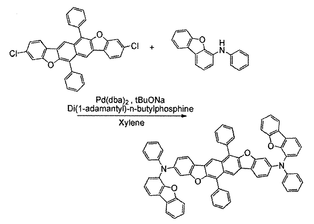
1H NMR(DMSO−d6,300MHz):δ=6.87(dd,J1=8.7Hz,J2=2.4Hz,2H),6.96(d,J1=2.4Hz,2H),7.10−7.18(m,6H),7.28−7.64(m,24H),7.94(d,J1=8.1Hz,2H),8.05(d,J1=7.8Hz,J2=1.5Hz,2H),8.16(dd,J1=6.9Hz,J2=1.5Hz,2H),8.24(s,2H).
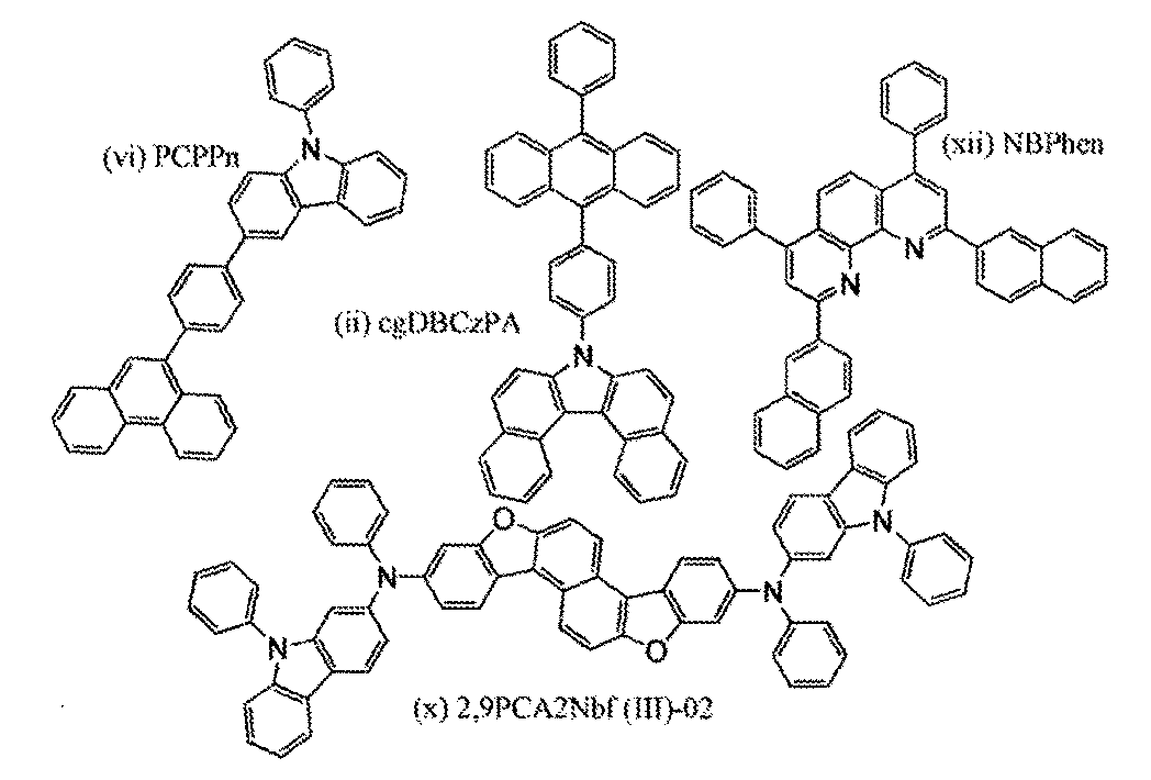
まず、ガラス基板上に、酸化珪素を含むインジウム錫酸化物(ITSO)をスパッタリング法にて成膜し、陽極101を形成した。なお、その膜厚は70nmとし、電極面積は4mm2(2mm×2mm)とした。
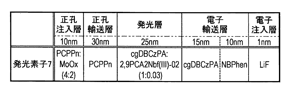


まず、ガラス基板上に、酸化珪素を含むインジウム錫酸化物(ITSO)をスパッタリング法にて成膜し、陽極101を形成した。なお、その膜厚は70nmとし、電極面積は4mm2(2mm×2mm)とした。
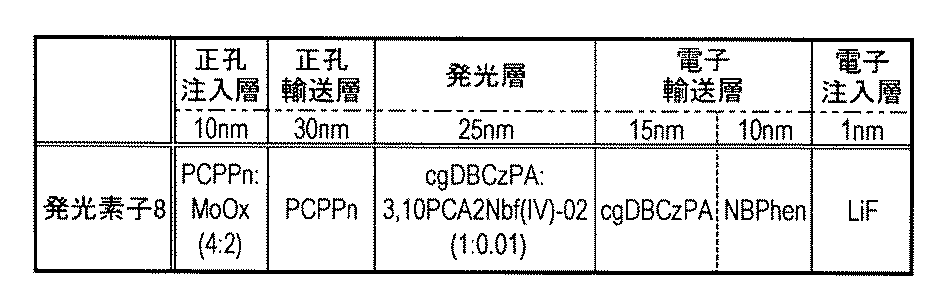

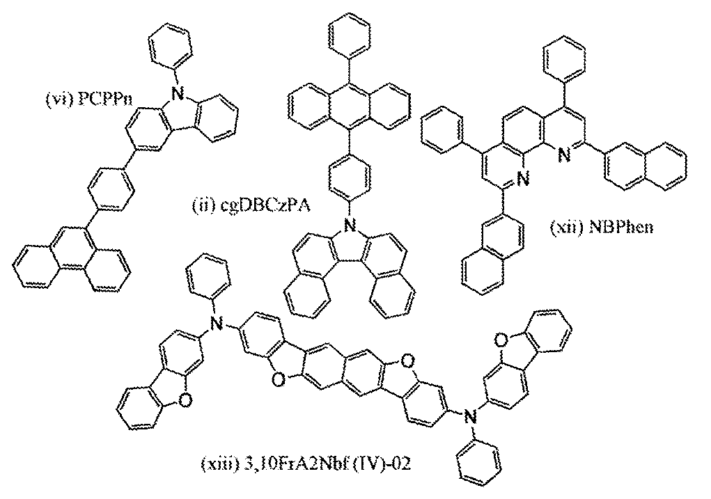
まず、ガラス基板上に、酸化珪素を含むインジウム錫酸化物(ITSO)をスパッタリング法にて成膜し、陽極101を形成した。なお、その膜厚は70nmとし、電極面積は4mm2(2mm×2mm)とした。



まず、ガラス基板上に、銀(Ag)とパラジウム(Pd)と銅(Cu)の合金膜(Ag−Pd−Cu(APC)膜)をスパッタリング法により、100nmの膜厚で成膜した後、酸化珪素を含むインジウム錫酸化物(ITSO)をスパッタリング法により、85nmの膜厚で成膜して陽極101を形成した。なお、その電極面積は4mm2(2mm×2mm)とした。
本合成例では、3,10−ビス[N−(9−フェニル−9H−カルバゾール−3−イル)−N−フェニルアミノ]ナフト[2,3−b;7,6−b’]ビスベンゾフラン(略称:3,10PCA2Nbf(II))の合成方法について詳しく説明する。3,10PCA2Nbf(II)の構造式を以下に示す。

200mL三口フラスコに3.0g(8.7mmol)の3,6−ジブロモ−2,7−ジメトキシナフタレンと、3.3g(19mmol)の4−クロロ−2−フルオロフェニルボロン酸と、5.8g(42mmol)の炭酸カリウムと、0.13g(0.43mmol)のトリス(2−メチルフェニル)ホスフィンを入れた。この混合物に、85mLのトルエンを加えた。この混合物を減圧しながら攪拌することで脱気した。この混合物に19mg(87μmol)の酢酸パラジウム(II)を加え、窒素気流下、60℃で14時間、120℃で11.5時間攪拌した。なお、当該撹拌の途中に、上記混合物へ3.0g(17mmol)の4−クロロ−2−フルオロフェニルボロン酸、4.8g(35mmol)の炭酸カリウムを加えた。
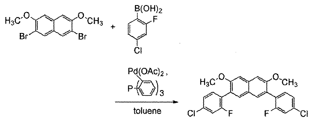
200mL三口フラスコに5.8g(13mmol)の3,6−ビス(4−クロロ−2−フルオロフェニル)−2,7−ジメトキシナフタレンを入れ、フラスコ内を窒素置換した。このフラスコに33mLのジクロロメタンを加えた。この溶液に29mLの三臭化ホウ素(約1.0mol/Lジクロロメタン溶液)と40mLのジクロロメタンを滴下した。滴下終了後、この溶液を室温で攪拌した。攪拌後、この溶液に氷冷下で約20mLの水を加えて、攪拌した。攪拌後、この混合物の水層をジクロロメタンで抽出し、抽出溶液と有機層を合わせて、水、飽和炭酸水素ナトリウム水溶液で洗浄した。有機層に硫酸マグネシウムを加え、水分を吸着した後この混合物を自然ろ過した。得られた濾液を濃縮し、白色固体を5.7g得た。ステップ2の合成スキームを以下に示す。

200mLの三口フラスコに2.5g(5.7mmol)の3,6−ビス(4−クロロ−2−フルオロフェニル)−2,7−ジヒドロキシナフタレンと7.6g(55mmol)の炭酸カリウムを入れた。この混合物に、N−メチル−2−ピロリドン137mLを加え、この混合物を減圧しながら攪拌することで脱気した。脱気後、この混合物を、窒素気流下、120℃で6時間攪拌した。撹拌後、この混合物に水を加え、析出した固体を濾取した。この固体を水、エタノールで洗浄した。得られた固体にエタノールを加え、加熱撹拌後、濾過して固体を得た。得られた固体をトルエンで再結晶し、白色固体を4.4g、収率86%で得た。ステップ3の合成スキームを以下に示す。

200mL三口フラスコに0.97g(2.6mmol)の3,10−ジクロロナフト[2,3−b;7,6−b’]ビスベンゾフランと、2.4g(6.4mmol)の3−アニリノ−9−フェニルカルバゾール、92mg(0.26mmol)のジ(1−アダマンチル)−n−ブチルホスフィン、1.5g(15mmol)のナトリウム tert−ブトキシドを入れた。この混合物に、25mLのキシレンを加えた。この混合物を減圧しながら攪拌することで脱気した。この混合物に30mg(51μmol)のビス(ジベンジリデンアセトン)パラジウム(0)を加え、窒素気流下、150℃で14.5時間攪拌した。

1H NMR(DMSO−d6,300MHz):δ=7.01(dd,J1=8.1Hz,J2=1.8Hz,2H),7.05−7.11(m,4H),7.17−7.26(m,6H),7.29−7.46(m,12H),7.52−7.57(m,2H),7.65−7.72(m,8H),8.06(d,J1=8.1Hz,2H),8.10(s,2H),8.16(d,J1=1.8Hz,2H),8.21(d,J1=7.8Hz,2H),8.61(s,2H).
本合成例では、実施の形態1で示した2,9−ビス[N−(ジベンゾフラン−3−イル)−N−フェニルアミノ]ナフト[2,1−b;6,5−b’]ビスベンゾフラン(略称:2,9FrA2Nbf(III)−02)の合成方法について詳細に説明する。2,9FrA2Nbf(III)−02の構造式を以下に示す。

実施例2における合成例2のステップ1と同様に合成した。
実施例2における合成例2のステップ2と同様に合成した。
200mL三口フラスコに1.2g(3.0mmol)の2,9−ジクロロナフト[2,1−b;6,5−b’]ビスベンゾフランと、2.0g(7.7mmol)のN−(ジベンゾフラン−3−イル)−N−フェニルアミン、0.11g(0.30mmol)のジ(1−アダマンチル)−n−ブチルホスフィン、1.8g(18mmol)のナトリウム tert−ブトキシドを入れた。この混合物に、30mLのキシレンを加えた。この混合物を減圧しながら攪拌することで脱気した。この混合物に35mg(60μmol)のビス(ジベンジリデンアセトン)パラジウム(0)を加え、窒素気流下、150℃で21.5時間攪拌した。撹拌後、この混合物に水、エタノールを加え、超音波を照射後、ろ過し、固体を得た。この固体をシリカゲルカラムクロマトグラフィー(展開溶媒:トルエン)で精製した。得られた固体をトルエンで2回再結晶し、黄色固体を1.5g、収率62%で得た。得られた固体1.5gをトレインサブリメーション法により昇華精製した。圧力1.9×10⁻²Pa、アルゴン流量0mL/minの条件で、365℃で加熱して行った。昇華精製後、黄色固体を1.2g、回収率82%で得た。ステップ3の合成スキームを以下に示す。
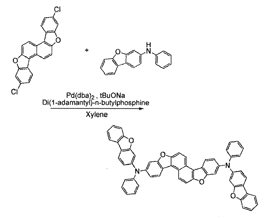
1H NMR(CD2Cl2,300MHz):δ=7.11−7.17(m,2H),7.20(dd,J1=8.4Hz,J2=2.1Hz,2H),7.24−7.28(m,4H),7.30−7.45(m,12H),7.46(d,J1=2.4Hz,2H),7.53(d,J1=8.4Hz,2H),7.87(d,J1=8.1Hz,2H),7.91−7.96(m,4H),8.33(d,J1=8.4Hz,2H),8.64(d,J1=9.3Hz,2H).
なお、m/z=563付近のプロダクトイオンは、2,9FrA2Nbf(III)−02におけるN−(ジベンゾフラン−3−イル)−N−フェニルアミノ基が離脱した状態のカチオンと推定され、2,9FrA2Nbf(III)−02が、N−(ジベンゾフラン−3−イル)−N−フェニルアミノ基を含んでいることを示唆するものである。また、m/z=258付近のプロダクトイオンは、2,9FrA2Nbf(III)−02における2−[N−(ジベンゾフラン−3−イル)−N−フェニルアミノ]ナフト[2,1−b;6,5−b’]ビスベンゾフラニル基が離脱した状態のカチオンと推定され、2,9FrA2Nbf(III)−02が、2−[N−(ジベンゾフラン−3−イル)−N−フェニルアミノ]ナフト[2,1−b;6,5−b’]ビスベンゾフラニル基を含んでいることを示唆するものである。
本合成例では、本発明の一態様の有機化合物である2,9−ビス[N−(ジベンゾフラン−4−イル)−N−フェニルアミノ]−6,13−ジフェニルナフト[2,1−b;6,5−b’]ビスベンゾフラン(略称:ph−2,9FrA2Nbf(III)−II)の合成方法について詳細に説明する。ph−2,9FrA2Nbf(III)−IIの構造式を以下に示す。

200mL三口フラスコに3.1g(7.1mmol)の3,7−ジヨード−2,6−ジメトキシナフタレンと、3.5g(16mmol)のフェニルボロン酸、4.3g(31mmol)の炭酸カリウム、0.22g(0.72mmol)のトリス(2−メチルフェニル)ホスフィンを入れ、フラスコ内を窒素置換した。この混合物に、50mLのトルエンを加えた。この混合物を減圧しながら攪拌することで脱気した。この混合物に43mg(0.14mmol)の酢酸パラジウム(II)を加え、窒素気流下、120℃で7時間攪拌した。撹拌後、この混合物にトルエンを加え、フロリジール、セライト、アルミナを通して吸引ろ過し、濾液を得た。濾液を濃縮して固体を得た。得られた固体をシリカゲルカラムクロマトグラフィー(展開溶媒:トルエン)で精製した。得られた固体をトルエンと酢酸エチルの混合溶媒で再結晶し、淡黄色固体を2.2g、収率90%で得た。ステップ1の合成スキームを以下に示す。

1H NMR(DMSO−d6,300MHz):δ=3.85(s,6H),7.34−7.49(m,8H),7.55−7.59(m,4H),7.77(s,2H).
100mL三口フラスコに2.2g(6.4mmol)の2,6−ジメトキシ−3,7−ジフェニルナフタレンを入れ、フラスコ内を窒素置換した。このフラスコに16mLのジクロロメタンを加えた。この溶液に14mL(14mmol)の三臭化ホウ素(約1.0mol/Lジクロロメタン溶液)と10mLのジクロロメタンを滴下した。滴下終了後、この溶液を室温で終夜攪拌した。攪拌後、この溶液に氷冷下で約20mLの水を加えて、攪拌した。攪拌後、この混合物の水層をジクロロメタンで抽出し、抽出溶液と有機層を合わせて、水、飽和炭酸水素ナトリウム水溶液で洗浄した。有機層を硫酸マグネシウムにより乾燥し、乾燥後この混合物を自然ろ過した。得られた濾液を濃縮し、白色固体を得た。
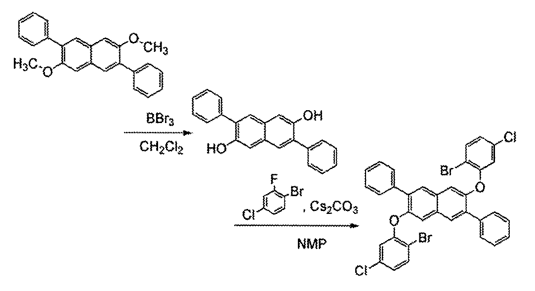
1H NMR(DMSO−d6,300MHz):δ=7.06(d,J1=2.4Hz,2H),7.16(dd,J1=9.0Hz,J2=2.4Hz,2H),7.32−7.46(m,6H),7.54(s,2H),7.67−7.35(m,6H),8.08(s,2H).
200mLの三口フラスコに1.8g(2.7mmol)の2,6−ビス(2−ブロモ−5−クロロフェノキシ)−3,7−ジフェニルナフタレンと0.14g(0.53mol)のトリフェニルホスフィン、2.1g(6.4mmol)の炭酸セシウムを入れた。この混合物に、N−メチル−2−ピロリドン20mLを加え、この混合物を減圧しながら攪拌することで脱気した。脱気後、この混合物を、窒素気流下、120℃で15.5時間攪拌した。撹拌後、混合物に水を加え、超音波を照射後、濾過して固体を得た。得られた固体をトルエンに溶解させ、フロリジール、セライト、アルミナを通して吸引ろ過し、濾液を得た。得られた濾液を濃縮して固体を得た。得られた固体をトルエンで再結晶し、淡黄色固体を1.1g、収率76%で得た。ステップ3の合成スキームを以下に示す。
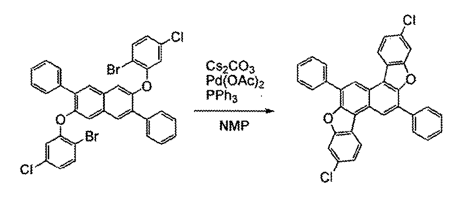
1H NMR(1,1,2,2−Tetrachloroethane−D2,300MHz):δ=7.56−7.74(m,8H),7.86(d,J1=2.1Hz,2H),8.13(d,J1=7.5Hz,4H),8.46(d,J1=8.7Hz,2H),8.84(s,2H).
200mL三口フラスコに1.1g(2.0mmol)の2,9−ジクロロ−6,13−ジフェニルナフト[2,1−b;6,5−b’]ビスベンゾフランと、1.3g(5.0mmol)のN−(ジベンゾフラン−4−イル)−N−フェニルアミン、71mg(0.20mmol)のジ(1−アダマンチル)−n−ブチルホスフィン、1.1g(12mmol)のナトリウム tert−ブトキシドを入れた。この混合物に、20mLのキシレンを加えた。この混合物を減圧しながら攪拌することで脱気した。この混合物に21mg(40μmol)のビス(ジベンジリデンアセトン)パラジウム(0)を加え、窒素気流下、150℃で27時間攪拌した。撹拌後、この混合物に水、エタノールを加え、超音波を照射後、ろ過し、固体を得た。

1H NMR(CD2Cl2,300MHz):δ=7.12(tt,J1=6.9Hz,J2=1.5Hz,2H),7.23−7.28(m,6H),7.30−7.48(m,18H),7.53−7.58(m,4H),7.87(dd,J1=6.9Hz,J2=1.5Hz,2H),7.99−8.06(m,6H),8.37(d,J1=8.7Hz,2H),8.72(s,2H).
また、m/z=257付近のプロダクトイオンは、ph−2,9FrA2Nbf(III)−IIにおける2−[N−(ジベンゾフラン−4−イル)−N−フェニルアミノ]−6,13−ジフェニルナフト[2,1−b;6,5−b’]ビスベンゾフラニル基が離脱した状態のカチオンと推定され、ph−2,9FrA2Nbf(III)−IIが、2−[N−(ジベンゾフラン−4−イル)−N−フェニルアミノ]−6,13−ジフェニルナフト[2,1−b;6,5−b’]ビスベンゾフラニル基を含んでいることを示唆するものである。
本合成例では、3,10−ビス[N−(ジベンゾフラン−3−イル)−N−フェニルアミノ]−6,13−ジフェニルナフト[2,3−b;6,7−b’]ビスベンゾフラン(略称:ph−3,10FrA2Nbf(IV)−02)の合成方法について詳細に説明する。ph−3,10FrA2Nbf(IV)−02の構造式を以下に示す。

実施例13における合成例7のステップ1と同様に合成した。
実施例13における合成例7のステップ2と同様に合成した。
実施例13における合成例7のステップ3と同様に合成した。
200mL三口フラスコに1.4g(2.6mmol)の3,10−ジクロロ−6,13−ジフェニルナフト[2,3−b;6,7−b’]ビスベンゾフランと、1.7g(6.4mmol)のN−(ジベンゾフラン−3−イル)−N−フェニルアミン、92mg(0.26mmol)のジ(1−アダマンチル)−n−ブチルホスフィン、1.5g(15mmol)のナトリウム tert−ブトキシドを入れた。この混合物に、25mLのキシレンを加えた。この混合物を減圧しながら攪拌することで脱気した。この混合物に29mg(51μmol)のビス(ジベンジリデンアセトン)パラジウム(0)を加え、窒素気流下、150℃で14.5時間攪拌した。撹拌後、この混合物にトルエンを加え、フロリジール、セライト、アルミナを通して吸引ろ過し、濾液を得た。得られた濾液を濃縮し固体を得た。この固体をシリカゲルカラムクロマトグラフィー(展開溶媒:トルエン:ヘキサン=1:2、次いでトルエン:ヘキサン=2:3)で精製し、固体を得た。

1H NMR(CD2Cl2,300MHz):δ=7.06−7.21(m,12H),7.29−7.36(m,8H),7.41(dt,J1=1.5Hz,J2=7.5Hz,2H),7.50−7.57(m,4H),7.60−7.70(m,8H),7.79−7.85(m,4H),7.90(dd,J1=7.2Hz,J2=0.9Hz,2H),8.34(s,2H).
本合成例では、3,10−ビス[N−(ジベンゾフラン−3−イル)−N−(4−イソプロピルフェニル)アミノ]ナフト[2,3−b;6,7−b’]ビスベンゾフラン(略称:3,10iPrFrA2Nbf(IV)−02)の合成方法について詳細に説明する。3,10iPrFrA2Nbf(IV)−02の構造式を以下に示す。

実施例1における合成例1のステップ1と同様に合成した。
実施例1における合成例1のステップ2と同様に合成した。
実施例1における合成例1のステップ3と同様に合成した。
200mL三口フラスコに1.0g(2.8mmol)の3,10−ジクロロナフト[2,3−b;6,7−b’]ビスベンゾフランと、2.1g(6.9mmol)のN−(4−イソプロピルフェニル)−N−(ジベンゾフラン−3−イル)アミン、99mg(0.28mmol)のジ(1−アダマンチル)−n−ブチルホスフィン、1.6g(17mmol)のナトリウム tert−ブトキシドを入れた。この混合物に、30mLのキシレンを加えた。この混合物を減圧しながら攪拌することで脱気した。この混合物に32mg(55μmol)のビス(ジベンジリデンアセトン)パラジウム(0)を加え、窒素気流下、150℃で15時間攪拌した。

1H NMR(CD2Cl2,300MHz):δ=1.29(d,J1=7.5Hz,12H),2.94(sep,J1=7.5Hz,2H),7.12−7.26(m,14H),7.32−7.37(m,4H),7.42(dt,J1=7.2Hz,J2=1.5Hz,2H),7.53(d,J1=7.8Hz,2H),7.86(d,J1=8.7Hz,2H),7.90−7.95(m,4H),8.00(s,2H),8.40(s,2H).
本合成例では、3,10−ビス[N−(ジベンゾチオフェン−2−イル)−N−フェニルアミノ]ナフト[2,3−b;6,7−b’]ビスベンゾフラン(略称:3,10ThA2Nbf(IV))の合成方法について詳細に説明する。3,10ThA2Nbf(IV)の構造式を以下に示す。

実施例1における合成例1のステップ1と同様に合成した。
実施例1における合成例1のステップ2と同様に合成した。
実施例1における合成例1のステップ3と同様に合成した。
200mL三口フラスコに1.1g(2.9mmol)の3,10−ジクロロナフト[2,3−b;6,7−b’]ビスベンゾフランと、2.0g(7.3mmol)のN−(ジベンゾチオフェン−2−イル)−N−フェニルアミン、0.11g(0.29mmol)のジ(1−アダマンチル)−n−ブチルホスフィン、1.7g(18mmol)のナトリウム tert−ブトキシドを入れた。この混合物に、30mLのキシレンを加えた。この混合物を減圧しながら攪拌することで脱気した。この混合物に34mg(58μmol)のビス(ジベンジリデンアセトン)パラジウム(0)を加え、窒素気流下、150℃で29時間攪拌した。
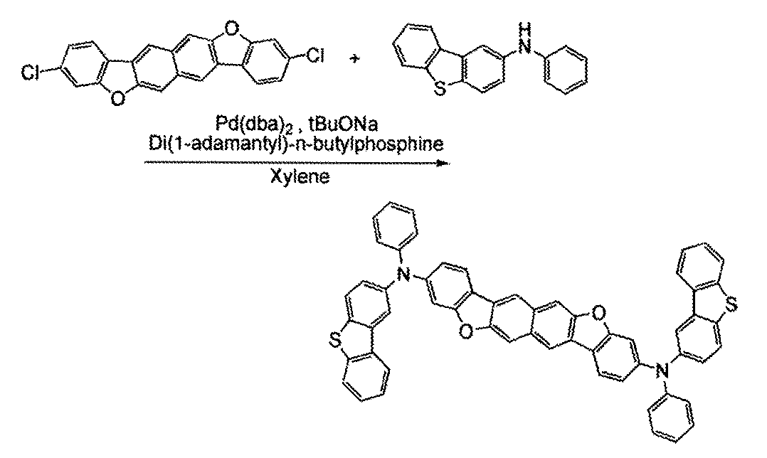
本合成例では、2,9−ビス{N−[4−(9−フェニル−9H−カルバゾール−3−イル)フェニル]−N−フェニルアミノ}ナフト[2,1−b;6,5−b’]ビスベンゾフラン(略称:2,9PCBA2Nbf(III))の合成方法について詳細に説明する。2,9PCBA2Nbf(III)の構造式を以下に示す。
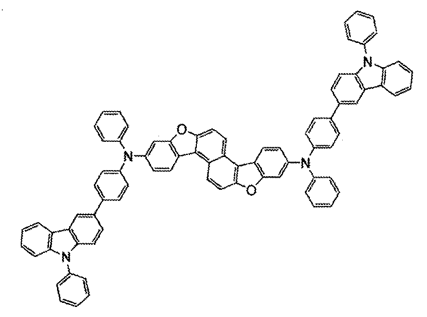
実施例2における合成例2のステップ1と同様に合成した。
実施例2における合成例2のステップ2と同様に合成した。
200mL三口フラスコに0.84g(2.2mmol)の2,9−ジクロロナフト[2,1−b;6,5−b’]ビスベンゾフランと、2.3g(5.6mmol)の3−[4−(4−フェニルアミノ)フェニル]−9−フェニルカルバゾール、80mg(0.22mmol)のジ(1−アダマンチル)−n−ブチルホスフィン、1.3g(13mmol)のナトリウム tert−ブトキシドを入れた。この混合物に、25mLのキシレンを加えた。この混合物を減圧しながら攪拌することで脱気した。この混合物に26mg(44μmol)のビス(ジベンジリデンアセトン)パラジウム(0)を加え、窒素気流下、150℃で20時間攪拌した。

1H NMR(CD2Cl2,300MHz):δ=7.13(t,J1=6.9Hz,2H),7.25−7.40(m,16H),7.43−7.54(m,10H),7.60−7.73(m,14H),7.97(d,J1=9.3Hz,2H),8.22(d,J1=7.8Hz,2H),8.34(d,J1=8.7Hz,2H),8.40(d,J1=1.5Hz,2H),8.66(d,J1=8.7Hz,2H).
本合成例では、3,10−ビス[N−(ジベンゾフラン−3−イル)−N−(3,5−ジ−t−ブチルフェニル)アミノ]ナフト[2,3−b;6,7−b’]ビスベンゾフラン(略称:3,10mmtBuFrA2Nbf(IV)−02)の合成方法について詳細に説明する。3,10mmtBuFrA2Nbf(IV)−02の構造式を以下に示す。
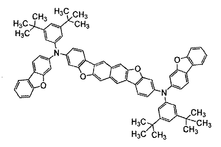
実施例1における合成例1のステップ1と同様に合成した。
実施例1における合成例1のステップ2と同様に合成した。
実施例1における合成例1のステップ3と同様に合成した。
200mL三口フラスコに4.2g(17mmol)の3−ブロモジベンゾフラン、5.2g(25mmol)の3,5−ジ−tert−ブチルアニリン、4.9g(51mmol)のナトリウム tert−ブトキシドを入れた。この混合物にトルエン85mL、トリ(tert−ブチル)ホスフィンの10%ヘキサン溶液0.3mLを加え、混合物を減圧しながら攪拌することで脱気した。この混合物にビス(ジベンジリデンアセトン)パラジウム(0)を98mg(0.17mmol)加え、窒素気流下にて120℃で7時間加熱撹拌した。撹拌後、この混合物にトルエンを加え、フロリジール、セライト、アルミナを通して吸引ろ過し、濾液を濃縮して固体を得た。この固体をシリカゲルカラムクロマトグラフィー(展開溶媒:トルエン:ヘキサン=1:3)で精製した。得られた固体をエタノールで再結晶し、白色固体を3.7g、収率59%で得た。ステップ4の合成スキームを以下に示す。
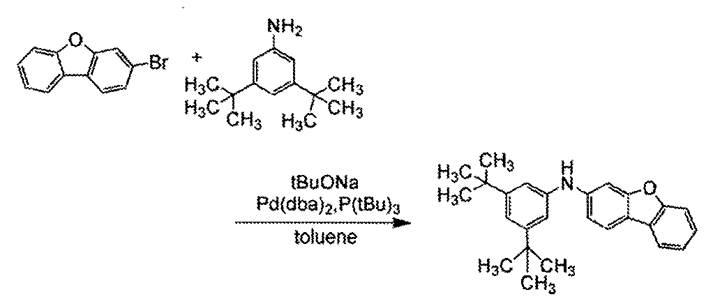
1H NMR(DMSO−d6,300MHz):δ=1.29(s,18H),6.99(t,J1=1.2Hz,1H),7.03−7.07(m,3H),7.24(d,J1=2.1Hz,1H),7.28−7.39(m,2H),7.58(dd,J1=7.2Hz,J2=1.5Hz,1H),7.89−7.95(m,2H),8.48(s,1H).
200mL三口フラスコに0.90g(2.4mmol)の3,10−ジクロロナフト[2,3−b;6,7−b’]ビスベンゾフランと、2.2g(6.0mmol)のN−(ジベンゾフラン−3−イル)−N−(3,5−ジ−tert−ブチルフェニル)アミン、86mg(0.28mmol)のジ(1−アダマンチル)−n−ブチルホスフィン、1.4g(14mmol)のナトリウム tert−ブトキシドを入れた。この混合物に、25mLのキシレンを加えた。この混合物を減圧しながら攪拌することで脱気した。この混合物に27mg(48μmol)のビス(ジベンジリデンアセトン)パラジウム(0)を加え、窒素気流下、150℃で27時間攪拌した。
1H NMR(CD2Cl2,300MHz):δ=1.28(s,36H),7.10−7.15(m,6H),7.19(dd,J1=8.7Hz,J2=1.8Hz,2H),7.25−7.26(m,4H),7.31−7.37(m,4H),7.41(dt,J1=8.4Hz,J2=1.5Hz,2H),7.52(d,J1=7.8Hz,2H),7.86(d,J1=8.4Hz,2H),7.90−7.94(m,4H),8.00(s,2H),8.39(s,2H).
本合成例では、実施の形態1で示した本発明の一態様の有機化合物である3,10−ビス{N−[4−(ジベンゾフラン−4−イル)フェニル]−N−フェニルアミノ}ナフト[2,3−b;6,7−b’]ビスベンゾフラン(略称:3,10FrBA2Nbf(IV)−II)の合成方法について詳細に説明する。3,10FrBA2Nbf(IV)−IIの構造式を以下に示す。
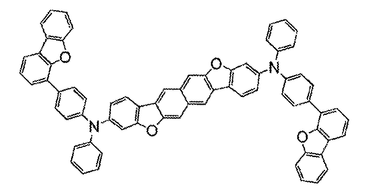
実施例1における合成例1のステップ1と同様に合成した。
実施例1における合成例1のステップ2と同様に合成した。
実施例1における合成例1のステップ3と同様に合成した。
200mL三口フラスコに1.0g(2.6mmol)の3,10−ジクロロナフト[2,3−b;6,7−b’]ビスベンゾフランと、2.2g(6.4mmol)の4−(ジベンゾフラン−4−イル)ジフェニルアミン、93mg(0.26mmol)のジ(1−アダマンチル)−n−ブチルホスフィン、1.5g(15mmol)のナトリウム tert−ブトキシドを入れた。この混合物に、25mLのキシレンを加えた。この混合物を減圧しながら攪拌することで脱気した。この混合物に29mg(52μmol)のビス(ジベンジリデンアセトン)パラジウム(0)を加え、窒素気流下、150℃で13時間攪拌した。
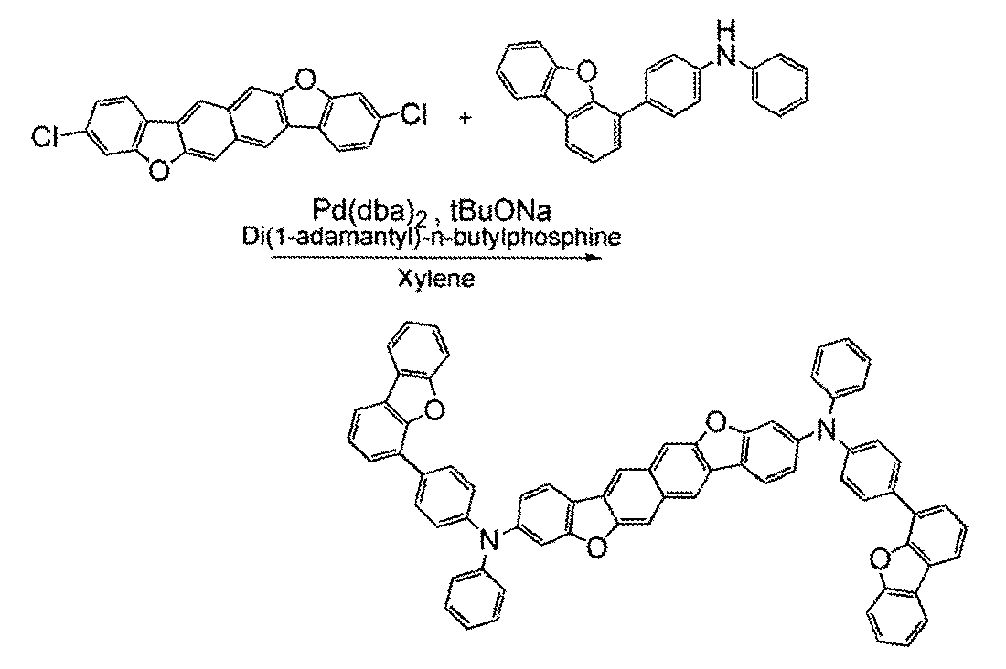
1H NMR(CD2Cl2,300MHz):δ=7.14−7.21(m,4H),7.27−7.44(m,16H),7.46−7.53(m,4H),7.62−7.67(m,4H),7.89−7.92(m,4H),7.95−7.99(m,4H),8.02−8.05(m,4H),8.43(s,2H).
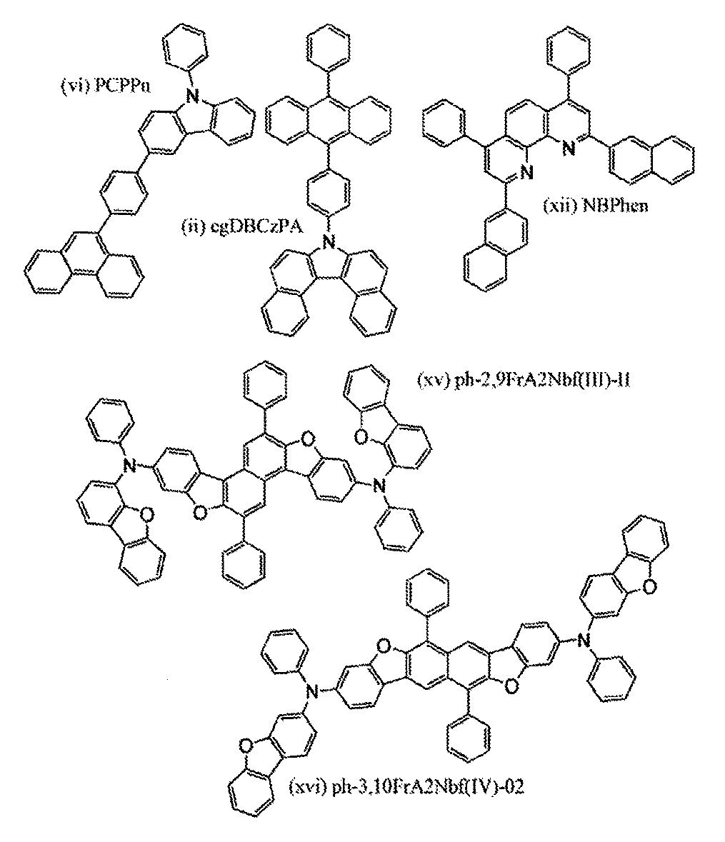
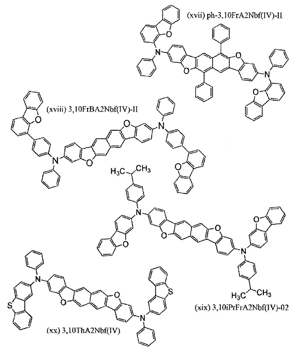
まず、ガラス基板上に、酸化珪素を含むインジウム錫酸化物(ITSO)をスパッタリング法にて成膜し、陽極101を形成した。なお、その膜厚は70nmとし、電極面積は4mm2(2mm×2mm)とした。
発光素子11は、発光素子10におけるph−2,9FrA2Nbf(III)−IIを、上記構造式(xvi)で表される3,10−ビス[N−(ジベンゾフラン−3−イル)−N−フェニルアミノ]−6,13−ジフェニルナフト[2,3−b;6,7−b’]ビスベンゾフラン(略称:ph−3,10FrA2Nbf(IV)−02)に替えた他は発光素子10と同様に作製した。
発光素子12は、発光素子10におけるph−2,9FrA2Nbf(III)−IIを、上記構造式(xvii)で表される3,10−ビス[N−(ジベンゾフラン−4−イル)−N−フェニルアミノ]−6,13−ジフェニルナフト[2,3−b;6,7−b’]ビスベンゾフラン(略称:ph−3,10FrA2Nbf(IV)−II)に替えた他は発光素子10と同様に作製した。
発光素子13は、発光素子10におけるph−2,9FrA2Nbf(III)−IIを、上記構造式(xviii)で表される3,10−ビス{N−[4−(ジベンゾフラン−4−イル)フェニル]−N−フェニルアミノ}ナフト[2,3−b;6,7−b’]ビスベンゾフラン(略称:3,10FrBA2Nbf(IV)−II)に替えた他は発光素子10と同様に作製した。
発光素子14は発光素子10におけるph−2,9FrA2Nbf(III)−IIを、上記構造式(xix)で表される3,10−ビス[N−(ジベンゾフラン−3−イル)−N−(4−イソプロピルフェニル)アミノ]ナフト[2,3−b;6,7−b’]ビスベンゾフラン(略称:3,10iPrFrA2Nbf(IV)−02)に替えた他は発光素子10と同様に作製した。
発光素子15は発光素子10におけるph−2,9FrA2Nbf(III)−IIを、上記構造式(xx)で表される3,10−ビス[N−(ジベンゾチオフェン−2−イル)−N−フェニルアミノ]ナフト[2,3−b;6,7−b’]ビスベンゾフラン(略称:3,10ThA2Nbf(IV))に替えた他は発光素子10と同様に作製した。
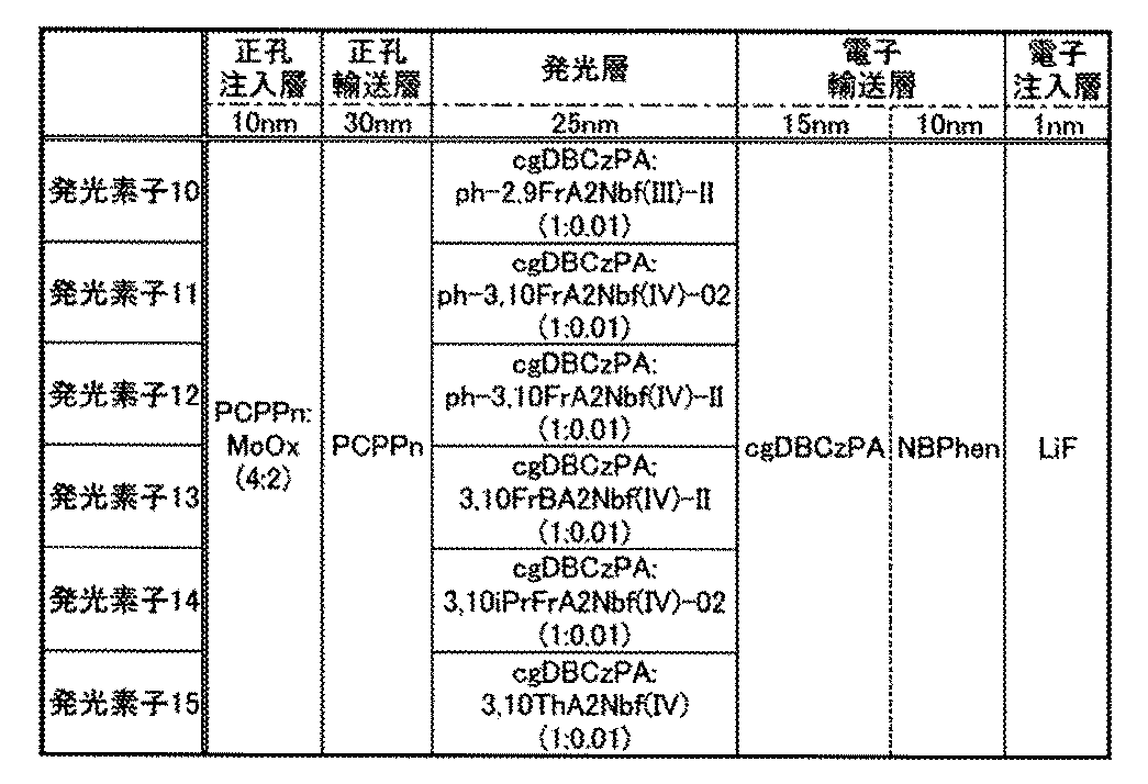
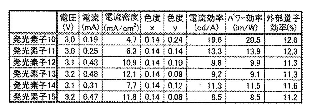
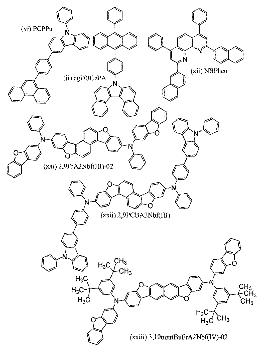
まず、ガラス基板上に、酸化珪素を含むインジウム錫酸化物(ITSO)をスパッタリング法にて成膜し、陽極101を形成した。なお、その膜厚は70nmとし、電極面積は4mm2(2mm×2mm)とした。
発光素子17は、発光素子16における2,9FrA2Nbf(III)−02を、上記構造式(xxii)で表される2,9−ビス{N−[4−(9−フェニル−9H−カルバゾール−3−イル)フェニル]−N−フェニルアミノ}ナフト[2,1−b;6,5−b’]ビスベンゾフラン(略称:2,9PCBA2Nbf(III))に替え、cgDBCzPAとの重量比を1:0.01(=cgDBCzPA:2,9PCBA2Nbf(III))とした他は発光素子16と同様に作製した。
発光素子18は、発光素子16における2,9FrA2Nbf(III)−02を、上記構造式(xxiii)で表される3,10−ビス[N−(ジベンゾフラン−3−イル)−N−(3,5−ジ−t−ブチルフェニル)アミノ]ナフト[2,3−b;6,7−b’]ビスベンゾフラン(略称:3,10mmtBuFrA2Nbf(IV)−02)に替え、cgDBCzPAとの重量比を1:0.01(=cgDBCzPA:3,10mmtBuFrA2Nbf(IV)−02)とした他は発光素子16と同様に作製した。

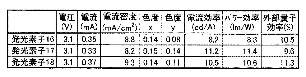
102 陰極
103 EL層
111 正孔注入層
112 正孔輸送層
113 発光層
114 電子輸送層
115 電子注入層
116 電荷発生層
117 P型層
118 電子リレー層
119 電子注入バッファ層
400 基板
401 第1の電極
403 EL層
404 第2の電極
405 シール材
406 シール材
407 封止基板
412 パッド
420 ICチップ
501 第1の電極
502 第2の電極
503 EL層
511 第1の発光ユニット
512 第2の発光ユニット
513 電荷発生層
601 駆動回路部(ソース線駆動回路)
602 画素部
603 駆動回路部(ゲート線駆動回路)
604 封止基板
605 シール材
607 空間
608 配線
609 FPC(フレキシブルプリントサーキット)
610 素子基板
611 スイッチング用FET
612 電流制御用FET
613 第1の電極
614 絶縁物
616 EL層
617 第2の電極
618 発光素子
623 nチャネル型FET
624 pチャネル型FET
730 絶縁膜
770 平坦化絶縁膜
772 導電膜
782 発光素子
783 液滴吐出装置
784 液滴
785 層
786 発光物質を含む層
788 導電膜
901 筐体
902 液晶層
903 バックライトユニット
904 筐体
905 ドライバIC
906 端子
951 基板
952 電極
953 絶縁層
954 隔壁層
955 EL層
956 電極
1001 基板
1002 下地絶縁膜
1003 ゲート絶縁膜
1006 ゲート電極
1007 ゲート電極
1008 ゲート電極
1020 第1の層間絶縁膜
1021 第2の層間絶縁膜
1022 電極
1024W 発光素子の第1の電極
1024R 発光素子の第1の電極
1024G 発光素子の第1の電極
1024B 発光素子の第1の電極
1025 隔壁
1028 EL層
1029 陰極
1031 封止基板
1032 シール材
1033 透明な基材
1034R 赤色の着色層
1034G 緑色の着色層
1034B 青色の着色層
1035 黒色層(ブラックマトリックス)
1036 オーバーコート層
1037 第3の層間絶縁膜
1040 画素部
1041 駆動回路部
1042 周辺部
1400 液滴吐出装置
1402 基板
1403 液滴吐出手段
1404 撮像手段
1405 ヘッド
1406 点線
1407 制御手段
1408 記憶媒体
1409 画像処理手段
1410 コンピュータ
1411 マーカー
1412 ヘッド
1413 材料供給源
1414 材料供給源
1415 材料供給源
1416 ヘッド
2001 筐体
2002 光源
3001 照明装置
5000 表示領域
5001 表示領域
5002 表示領域
5003 表示領域
5004 表示領域
5005 表示領域
7101 筐体
7103 表示部
7105 スタンド
7107 表示部
7109 操作キー
7110 リモコン操作機
7201 本体
7202 筐体
7203 表示部
7204 キーボード
7205 外部接続ポート
7206 ポインティングデバイス
7210 第2の表示部
7401 筐体
7402 表示部
7403 操作ボタン
7404 外部接続ポート
7405 スピーカ
7406 マイク
9033 留め具
9034 スイッチ
9035 電源スイッチ
9036 スイッチ
9310 携帯情報端末
9311 表示パネル
9312 表示領域
9313 ヒンジ
9315 筐体
9630 筐体
9631 表示部
9631a 表示部
9631b 表示部
9632a タッチパネル領域
9632b タッチパネル領域
9633 太陽電池
9634 充放電制御回路
9635 バッテリー
9636 DCDCコンバータ
9637 操作キー
9638 コンバータ
9639 ボタン
Claims (36)
- 下記一般式(G1)で表される有機化合物。
(但し、式中Bは置換または無置換のナフトビスベンゾフラン骨格、置換または無置換のナフトビスベンゾチオフェン骨格および置換または無置換のナフトベンゾフラノベンゾチオフェン骨格のいずれかを表す。また、Ar1は置換または無置換の炭素数6乃至25の芳香族炭化水素基、置換または無置換のジベンゾフラニル基、置換または無置換のジベンゾチオフェニル基、および置換または無置換のカルバゾリル基のいずれかである。Aは置換または無置換のジベンゾフラニル基、置換または無置換のジベンゾチオフェニル基、および置換または無置換のカルバゾリル基のいずれかであり、α1乃至α3はそれぞれ独立に置換または無置換の炭素数6乃至25の二価の芳香族炭化水素基である。また、l、m、nはそれぞれ独立に0乃至2の整数を表し、qは1又は2である。)
- 請求項1において、前記1が0である有機化合物。
- 請求項1において、
下記一般式(G1−1)で表される有機化合物。
(但し上記一般式(G1−1)において、Bは下記一般式(B1−1)または(B3−1)で表される基である。また、Ar1は置換もしくは無置換の炭素数6乃至25の芳香族炭化水素基であり、Aは下記一般式(g0)で表される基である。また、mは0乃至2の整数を表す。また、α2は置換または無置換の炭素数6乃至14の二価の芳香族炭化水素基である。)
(但し、上記一般式(B1−1)または(B3−1)において、X2およびX3はそれぞれ独立に酸素原子または硫黄原子を表す。また、R12,R18、R52およびR58は単結合を表す。)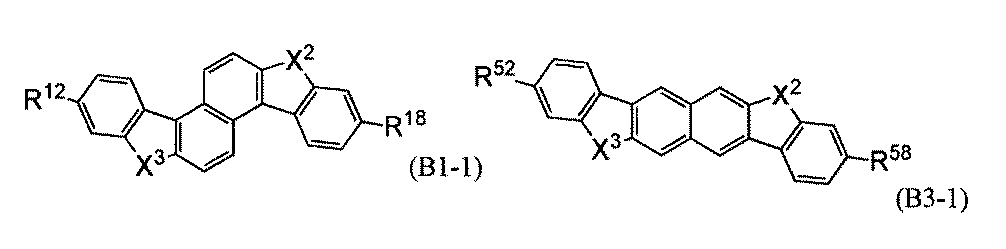
(但し、上記一般式(g0)において、X0は酸素原子、または、置換もしくは無置換のフェニル基が結合した窒素原子である。また、R2は単結合を表す。)
- 請求項1において、分子量が1300以下である前記有機化合物。
- 請求項1において、分子量が1000以下である前記有機化合物。
- 請求項1において、
下記構造式(iii)、(vii)、(ix)、(x)、(xi)、(xiii)、(xv)、(xvi)、(xvii)、(xviii)、(xix)、(xx)、(xxi)、(xxii)、(xxiii)、(XXiv)のいずれかで表される有機化合物。

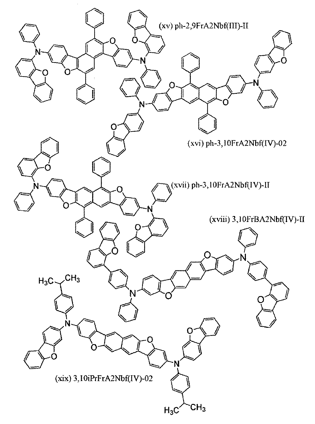

- 請求項1に記載の有機化合物を含む電子デバイス。
- 請求項1において、前記Bが、下記一般式(B1)乃至一般式(B4)で表される骨格のいずれかである有機化合物。
(但し、式中X2およびX3はそれぞれ独立に酸素原子または硫黄原子を表す。なお、上記一般式(B1)においては、R10乃至R21のいずれか1または2が単結合を表し、残りがそれぞれ独立に水素、炭素数1乃至10の炭化水素基、炭素数3乃至10の環式炭化水素基、置換または無置換の炭素数6乃至14の芳香族炭化水素基、置換または無置換の炭素数12乃至32のジアリールアミノ基のいずれかを表す。また、上記一般式(B2)においては、R30乃至R41のいずれか1または2が単結合を表し、残りがそれぞれ独立に水素、炭素数1乃至10の炭化水素基、炭素数3乃至10の環式炭化水素基、置換または無置換の炭素数6乃至14の芳香族炭化水素基、置換または無置換の炭素数12乃至32のジアリールアミノ基のいずれかを表す。また、上記一般式(B3)においては、R50乃至R61のいずれか1または2が単結合を表し、残りがそれぞれ独立に水素、炭素数1乃至10の炭化水素基、炭素数3乃至10の環式炭化水素基、置換または無置換の炭素数6乃至14の芳香族炭化水素基、置換または無置換の炭素数12乃至32のジアリールアミノ基のいずれかを表す。また、上記一般式(B4)においては、R70乃至R81のいずれか1または2が単結合を表し、残りがそれぞれ独立に水素、炭素数1乃至10の炭化水素基、炭素数3乃至10の環式炭化水素基、置換または無置換の炭素数6乃至14の芳香族炭化水素基、置換または無置換の炭素数12乃至32のジアリールアミノ基のいずれかを表す。)
- 請求項8において、前記Bが、前記一般式(B1)乃至一般式(B3)で表される骨格のいずれかである有機化合物。
- 請求項8において、前記X2およびX3が共に酸素原子である有機化合物。
- 請求項1において、前記Bが下記一般式(B1)で表される骨格である有機化合物。
(但し、式中X2およびX3はそれぞれ独立に酸素原子または硫黄原子を表す。また、R10乃至R21は、その1または2が単結合を表し、残りがそれぞれ独立に、水素、炭素数1乃至10の炭化水素基、炭素数3乃至10の環式炭化水素基、置換または無置換の炭素数6乃至14の芳香族炭化水素基、置換または無置換の炭素数12乃至32のジアリールアミノ基のいずれかを表す。)
- 請求項11において、前記一般式(B1)におけるR11、R12、R17およびR18のいずれか1または2が単結合を表す有機化合物。
- 請求項11において、前記一般式(G1)におけるqが2であり、前記一般式(B1)におけるR11またはR12のいずれか一方が単結合であり、R17またはR18のいずれか一方が単結合である有機化合物。
- 請求項11において、前記一般式(G1)におけるqが2であり、前記一般式(B1)におけるR11およびR17が単結合である有機化合物。
- 請求項11において、前記一般式(G1)におけるqが2であり、前記一般式(B1)におけるR12およびR18が単結合である有機化合物。
- 請求項1において、前記Bが下記一般式(B2)で表される骨格である有機化合物。
(但し、式中X2およびX3はそれぞれ独立に酸素原子または硫黄原子を表す。また、R30乃至R41は、その1または2が単結合を表し、残りがそれぞれ独立に、水素、炭素数1乃至10の炭化水素基、炭素数3乃至10の環式炭化水素基、置換または無置換の炭素数6乃至14の芳香族炭化水素基、置換または無置換の炭素数12乃至32のジアリールアミノ基のいずれかを表す。)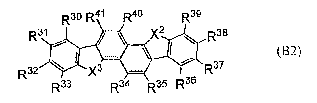
- 請求項16において、前記一般式(B2)におけるR31、R32、R37およびR38のいずれか1または2が単結合を表す有機化合物。
- 請求項16において、前記一般式(G1)におけるqが2であり、前記一般式(B2)におけるR31またはR32およびR37またはR38が単結合である有機化合物。
- 請求項16において、前記一般式(G1)におけるqが2であり、前記一般式(B2)におけるR31およびR37が単結合である有機化合物。
- 請求項16において、前記一般式(G1)におけるqが2であり、前記一般式(B2)におけるR32およびR38が単結合である有機化合物。
- 請求項1において、前記Bが下記一般式(B3)で表される骨格である有機化合物。
(但し、式中X2およびX3はそれぞれ独立に酸素原子または硫黄原子を表す。また、R50乃至R61は、その1または2が単結合を表し、残りがそれぞれ独立に、水素、炭素数1乃至10の炭化水素基、炭素数3乃至10の環式炭化水素基、置換または無置換の炭素数6乃至14の芳香族炭化水素基、置換または無置換の炭素数12乃至32のジアリールアミノ基のいずれかを表す。)
- 請求項21において、前記一般式(B3)におけるR51、R52、R57およびR58のいずれか1または2が単結合を表す有機化合物。
- 請求項21において、前記一般式(G1)におけるqが2であり、前記一般式(B3)におけるR51またはR52およびR57またはR58が単結合である有機化合物。
- 請求項21において、前記一般式(G1)におけるqが2であり、前記一般式(B3)におけるR51およびR57が単結合である有機化合物。
- 請求項21において、前記一般式(G1)におけるqが2であり、前記一般式(B3)におけるR52およびR58が単結合である有機化合物。
- 請求項1に記載の有機化合物を含む発光素子。
- 請求項26に記載の発光素子と、トランジスタ、または、基板と、を有する発光装置。
- 請求項27に記載の発光装置と、センサ、操作ボタン、スピーカ、または、マイクと、を有する電子機器。
- 請求項27に記載の発光装置と、筐体と、を有する照明装置。
- 請求項1において、前記Ar1が置換または無置換の炭素数6乃至25の芳香族炭化水素基である有機化合物。
- 請求項30において、
Ar1は下記一般式(g1)乃至(g3)で表される基のいずれかであり、Aは下記一般式(g1)乃至(g3)で表される基のいずれかである。また、α1乃至α3はそれぞれ独立に置換または無置換の炭素数6乃至14の二価の芳香族炭化水素基のいずれかである有機化合物。
(一般式(g1)乃至(g3)においては、R1乃至R9は、そのいずれか1が単結合を表し、残りがそれぞれ独立に水素、炭素数1乃至10の炭化水素基、炭素数3乃至10の環式炭化水素基、置換または無置換の炭素数6乃至14の芳香族炭化水素基のいずれかを表す。ただし、Aが一般式(g3)で表される基であり、且つ一般式(g3)で表される基におけるR9が単結合を表す場合、nは1または2であるものとする。また、Ar1が一般式(g3)で表される基であり、かつ(g3)においてR9が単結合を表す場合、mは1または2であるものとする。)
- 請求項31において、Aが一般式(g1)で表される基である有機化合物。
- 請求項31において、
Aおよび/またはAr1がそれぞれ独立に、前記一般式(g1)または一般式(g2)で表される基である場合、当該一般式(g1)または一般式(g2)で表される基においては、R1乃至R3のいずれかが単結合であり、
Aおよび/またはAr1が前記一般式(g3)で表される基である場合、当該一般式(g3)で表される基においてR2またはR3が単結合である有機化合物。 - 請求項31において、前記qが0である有機化合物。
- 請求項31において、
前記Aが前記一般式(g1)または前記一般式(g3)で表される基であり、
当該一般式(g1)または前記一般式(g3)で表される基におけるR2が単結合を表す有機化合物。 - 請求項32乃至請求項35において、前記nが0である有機化合物。
Priority Applications (15)
| Application Number | Priority Date | Filing Date | Title |
|---|---|---|---|
| JP2019510488A JP7143279B2 (ja) | 2017-04-07 | 2018-02-28 | 発光素子用材料、発光材料、発光素子、発光装置、電子機器、及び照明装置 |
| CN201880000701.1A CN109153685B (zh) | 2017-04-07 | 2018-02-28 | 有机化合物、发光元件、发光装置、电子设备、显示装置及照明装置 |
| KR1020207032787A KR102282832B1 (ko) | 2017-04-07 | 2018-02-28 | 유기 화합물, 발광 소자, 발광 장치, 전자 기기, 표시 장치, 및 조명 장치 |
| KR1020197037115A KR102180833B1 (ko) | 2017-04-07 | 2018-02-28 | 유기 화합물, 발광 소자, 발광 장치, 전자 기기, 표시 장치, 및 조명 장치 |
| DE112018000021.4T DE112018000021B4 (de) | 2017-04-07 | 2018-02-28 | Organische Verbindung und deren Verwendung in Licht emittierenden Elementen, Licht emittierenden Vorrichtungen, elektronischen Vorrichtungen, Anzeigevorrichtungen und Beleuchtungsvorrichtungen |
| KR1020227045617A KR102722655B1 (ko) | 2017-04-07 | 2018-02-28 | 유기 화합물, 발광 소자, 발광 장치, 전자 기기, 표시 장치, 및 조명 장치 |
| CN202211341943.1A CN115677715A (zh) | 2017-04-07 | 2018-02-28 | 有机化合物、发光元件、发光装置、电子设备、显示装置及照明装置 |
| KR1020217023120A KR102482720B1 (ko) | 2017-04-07 | 2018-02-28 | 유기 화합물, 발광 소자, 발광 장치, 전자 기기, 표시 장치, 및 조명 장치 |
| KR1020187026969A KR102269996B1 (ko) | 2017-04-07 | 2018-02-28 | 유기 화합물, 발광 소자, 발광 장치, 전자 기기, 표시 장치, 및 조명 장치 |
| US16/090,477 US11225488B2 (en) | 2017-04-07 | 2018-02-28 | Organic compound, light-emitting element, light-emitting device, electronic device, display device, and lighting device |
| CN202110224508.XA CN112961167B (zh) | 2017-04-07 | 2018-02-28 | 有机化合物、发光元件、发光装置、电子设备、显示装置及照明装置 |
| US17/574,752 US11834457B2 (en) | 2017-04-07 | 2022-01-13 | Organic compound, light-emitting element, light-emitting device, electronic device, display device, and lighting device |
| JP2022146293A JP2022179515A (ja) | 2017-04-07 | 2022-09-14 | 有機化合物 |
| US18/382,640 US12421202B2 (en) | 2017-04-07 | 2023-10-23 | Organic compound, light-emitting element, light-emitting device, electronic device, display device and lighting device |
| JP2024137796A JP2024164105A (ja) | 2017-04-07 | 2024-08-19 | 発光素子 |
Applications Claiming Priority (8)
| Application Number | Priority Date | Filing Date | Title |
|---|---|---|---|
| JP2017-077076 | 2017-04-07 | ||
| JP2017077076 | 2017-04-07 | ||
| JP2017-179894 | 2017-09-20 | ||
| JP2017179894 | 2017-09-20 | ||
| JP2017231424 | 2017-12-01 | ||
| JP2017-231424 | 2017-12-01 | ||
| JP2018-019531 | 2018-02-06 | ||
| JP2018019531 | 2018-02-06 |
Related Child Applications (2)
| Application Number | Title | Priority Date | Filing Date |
|---|---|---|---|
| US16/090,477 A-371-Of-International US11225488B2 (en) | 2017-04-07 | 2018-02-28 | Organic compound, light-emitting element, light-emitting device, electronic device, display device, and lighting device |
| US17/574,752 Continuation US11834457B2 (en) | 2017-04-07 | 2022-01-13 | Organic compound, light-emitting element, light-emitting device, electronic device, display device, and lighting device |
Publications (1)
| Publication Number | Publication Date |
|---|---|
| WO2018185571A1 true WO2018185571A1 (ja) | 2018-10-11 |
Family
ID=63712939
Family Applications (1)
| Application Number | Title | Priority Date | Filing Date |
|---|---|---|---|
| PCT/IB2018/051255 Ceased WO2018185571A1 (ja) | 2017-04-07 | 2018-02-28 | 有機化合物、発光素子、発光装置、電子機器、表示装置及び照明装置 |
Country Status (7)
| Country | Link |
|---|---|
| US (2) | US11834457B2 (ja) |
| JP (3) | JP7143279B2 (ja) |
| KR (5) | KR102282832B1 (ja) |
| CN (4) | CN109928980B (ja) |
| DE (1) | DE112018000021B4 (ja) |
| TW (3) | TWI701252B (ja) |
| WO (1) | WO2018185571A1 (ja) |
Cited By (5)
| Publication number | Priority date | Publication date | Assignee | Title |
|---|---|---|---|---|
| WO2019215540A1 (ja) * | 2018-05-11 | 2019-11-14 | 株式会社半導体エネルギー研究所 | 有機化合物、発光素子、発光装置、電子機器、表示装置及び照明装置 |
| WO2020152547A1 (en) * | 2019-01-22 | 2020-07-30 | Semiconductor Energy Laboratory Co., Ltd. | Light-emitting device, light-emitting apparatus, electronic device, and lighting device |
| JP2021095397A (ja) * | 2019-12-12 | 2021-06-24 | 株式会社半導体エネルギー研究所 | 有機化合物、光デバイス、発光デバイス、発光装置、電子機器および照明装置 |
| WO2021234491A1 (ja) * | 2020-05-20 | 2021-11-25 | 株式会社半導体エネルギー研究所 | 有機化合物、発光デバイス、発光装置、電子機器、表示装置、照明装置 |
| US11930703B2 (en) | 2017-03-17 | 2024-03-12 | Semiconductor Energy Laboratory Co., Ltd. | Organic compound, light-emitting element, light-emitting device, electronic device, display device, and lighting device |
Families Citing this family (8)
| Publication number | Priority date | Publication date | Assignee | Title |
|---|---|---|---|---|
| US12384796B2 (en) | 2016-06-03 | 2025-08-12 | Lg Chem, Ltd. | Electroactive compounds |
| KR102282832B1 (ko) * | 2017-04-07 | 2021-07-27 | 가부시키가이샤 한도오따이 에네루기 켄큐쇼 | 유기 화합물, 발광 소자, 발광 장치, 전자 기기, 표시 장치, 및 조명 장치 |
| JP6339749B1 (ja) | 2017-04-07 | 2018-06-06 | 株式会社半導体エネルギー研究所 | 有機化合物、発光素子、発光装置、電子機器、照明装置、及び電子デバイス |
| US11618757B2 (en) | 2017-10-20 | 2023-04-04 | Lg Chem, Ltd. | Polycyclic compound and organic light emitting element comprising same |
| TWI875882B (zh) * | 2019-12-12 | 2025-03-11 | 日商半導體能源研究所股份有限公司 | 有機化合物、發光器件、光學器件、發光裝置、電子裝置及照明設備 |
| US11543584B2 (en) * | 2020-07-14 | 2023-01-03 | Meta Platforms Technologies, Llc | Inorganic matrix nanoimprint lithographs and methods of making thereof with reduced carbon |
| CN114835663B (zh) * | 2022-06-07 | 2025-06-03 | 阜阳欣奕华新材料科技股份有限公司 | 一种萘并杂芳基类化合物、有机电致发光器件和显示装置 |
| CN118397665A (zh) * | 2024-04-08 | 2024-07-26 | 业泓科技(成都)有限公司 | 有机发光二极体显示装置和超音波指纹辨识装置 |
Citations (7)
| Publication number | Priority date | Publication date | Assignee | Title |
|---|---|---|---|---|
| JP2010059147A (ja) * | 2008-07-14 | 2010-03-18 | Gracel Display Inc | 新規の有機電界発光化合物およびこれを使用する有機電界発光素子 |
| JP2013234151A (ja) * | 2012-05-09 | 2013-11-21 | Idemitsu Kosan Co Ltd | 縮合多環芳香族化合物及びそれを用いた有機薄膜トランジスタ |
| JP2014045099A (ja) * | 2012-08-27 | 2014-03-13 | Fujifilm Corp | 有機薄膜トランジスタ、有機半導体薄膜および有機半導体材料 |
| WO2014061464A1 (ja) * | 2012-10-15 | 2014-04-24 | 富士フイルム株式会社 | 有機薄膜トランジスタ、有機半導体薄膜および有機半導体材料 |
| US20150108440A1 (en) * | 2013-10-22 | 2015-04-23 | Samsung Display Co., Ltd. | Condensed cyclic compound and organic light emitting device including the same |
| WO2016153198A1 (ko) * | 2015-03-26 | 2016-09-29 | 덕산네오룩스 주식회사 | 유기전기 소자용 화합물, 이를 이용한 유기전기소자 및 그 전자 장치 |
| WO2017030307A1 (ko) * | 2015-08-20 | 2017-02-23 | 덕산네오룩스 주식회사 | 유기전기 소자용 화합물, 이를 이용한 유기전기소자 및 그 전자 장치 |
Family Cites Families (26)
| Publication number | Priority date | Publication date | Assignee | Title |
|---|---|---|---|---|
| US7723722B2 (en) * | 2007-03-23 | 2010-05-25 | Semiconductor Energy Laboratory Co., Ltd. | Organic compound, anthracene derivative, and light-emitting element, light-emitting device, and electronic device using anthracene derivative |
| JP5284677B2 (ja) * | 2008-04-25 | 2013-09-11 | 山本化成株式会社 | 有機トランジスタ |
| KR102301756B1 (ko) | 2008-05-16 | 2021-09-15 | 가부시키가이샤 한도오따이 에네루기 켄큐쇼 | 트리아릴아민 유도체, 발광 물질, 발광 소자, 발광 장치 및 전자 기기 |
| JP5498681B2 (ja) * | 2008-10-02 | 2014-05-21 | 山本化成株式会社 | 有機トランジスタ |
| WO2011074231A1 (ja) * | 2009-12-14 | 2011-06-23 | 出光興産株式会社 | 多環縮環化合物及びそれを用いた有機薄膜トランジスタ |
| WO2011074232A1 (ja) * | 2009-12-14 | 2011-06-23 | 出光興産株式会社 | 多環縮環化合物、及び、それを用いた有機薄膜トランジスタ |
| US10570113B2 (en) | 2010-04-09 | 2020-02-25 | Semiconductor Energy Laboratory Co., Ltd. | Aromatic amine derivative, light-emitting element, light-emitting device, electronic device, and lighting device |
| KR102132588B1 (ko) | 2010-09-10 | 2020-07-10 | 가부시키가이샤 한도오따이 에네루기 켄큐쇼 | 발광 소자 및 전자기기 |
| FI123363B (fi) * | 2011-01-31 | 2013-03-15 | Clothing Plus Holding Oy | Tekstiilinen alusta fysikaalisen suureen mittaamiseksi |
| JP6100476B2 (ja) | 2012-04-27 | 2017-03-22 | ユー・ディー・シー アイルランド リミテッド | 有機電界発光素子、有機電界発光素子用材料並びに該有機電界発光素子を用いた発光装置、表示装置及び照明装置 |
| JP6312960B2 (ja) | 2012-08-03 | 2018-04-18 | 株式会社半導体エネルギー研究所 | 発光素子、発光装置、電子機器、照明装置及び複素環化合物 |
| KR101900287B1 (ko) | 2012-12-11 | 2018-09-19 | 덕산네오룩스 주식회사 | 유기전기 소자용 화합물, 이를 이용한 유기전기소자 및 그 전자 장치 |
| US9496503B2 (en) | 2013-03-25 | 2016-11-15 | Semiconductor Energy Laboratory Co., Ltd. | Organic compound, light-emitting element, light-emitting device, electronic device, and lighting device |
| KR102034819B1 (ko) | 2013-03-26 | 2019-10-21 | 가부시키가이샤 한도오따이 에네루기 켄큐쇼 | 유기 화합물, 발광 소자, 발광 장치, 표시 장치, 전자 기기 및 조명 장치 |
| US10032993B2 (en) | 2013-03-29 | 2018-07-24 | Nippon Steel & Sumikin Chemical Co., Ltd. | Aromatic heterocyclic compound, manufacturing method thereof, organic semiconductor material, and organic semiconductor device |
| JP2016225458A (ja) * | 2015-05-29 | 2016-12-28 | 三星ディスプレイ株式會社Samsung Display Co.,Ltd. | 有機電界発光素子 |
| JP6754176B2 (ja) * | 2015-06-23 | 2020-09-09 | 三星ディスプレイ株式會社Samsung Display Co.,Ltd. | 有機電界発光素子 |
| EP3133664A1 (en) * | 2015-08-18 | 2017-02-22 | Novaled GmbH | Triaryl amine thick layer doped with metal amides for use as hole injection layer for an organic light-emitting diode (oled) |
| WO2017048025A1 (ko) | 2015-09-18 | 2017-03-23 | 덕산네오룩스 주식회사 | 유기전기소자용 화합물, 이를 이용한 유기전기소자 및 그 전자 장치 |
| JP2017226607A (ja) * | 2016-06-21 | 2017-12-28 | 山本化成株式会社 | チオフェン化合物の製造方法 |
| US11239426B2 (en) * | 2016-11-23 | 2022-02-01 | Lg Chem, Ltd. | Electroactive compounds |
| KR20190129946A (ko) * | 2017-03-17 | 2019-11-20 | 가부시키가이샤 한도오따이 에네루기 켄큐쇼 | 유기 화합물, 발광 소자, 발광 장치, 전자 기기, 표시 장치, 및 조명 장치 |
| JP6339749B1 (ja) * | 2017-04-07 | 2018-06-06 | 株式会社半導体エネルギー研究所 | 有機化合物、発光素子、発光装置、電子機器、照明装置、及び電子デバイス |
| KR102282832B1 (ko) * | 2017-04-07 | 2021-07-27 | 가부시키가이샤 한도오따이 에네루기 켄큐쇼 | 유기 화합물, 발광 소자, 발광 장치, 전자 기기, 표시 장치, 및 조명 장치 |
| KR102078459B1 (ko) * | 2017-07-18 | 2020-02-17 | 주식회사 엘지화학 | 신규한 화합물 및 이를 포함하는 유기 발광 소자 |
| US11618757B2 (en) | 2017-10-20 | 2023-04-04 | Lg Chem, Ltd. | Polycyclic compound and organic light emitting element comprising same |
-
2018
- 2018-02-28 KR KR1020207032787A patent/KR102282832B1/ko active Active
- 2018-02-28 WO PCT/IB2018/051255 patent/WO2018185571A1/ja not_active Ceased
- 2018-02-28 KR KR1020187026969A patent/KR102269996B1/ko active Active
- 2018-02-28 CN CN201910304758.7A patent/CN109928980B/zh active Active
- 2018-02-28 KR KR1020217023120A patent/KR102482720B1/ko active Active
- 2018-02-28 KR KR1020197037115A patent/KR102180833B1/ko active Active
- 2018-02-28 JP JP2019510488A patent/JP7143279B2/ja active Active
- 2018-02-28 DE DE112018000021.4T patent/DE112018000021B4/de active Active
- 2018-02-28 KR KR1020227045617A patent/KR102722655B1/ko active Active
- 2018-02-28 CN CN202110224508.XA patent/CN112961167B/zh active Active
- 2018-02-28 CN CN202211341943.1A patent/CN115677715A/zh active Pending
- 2018-02-28 CN CN201880000701.1A patent/CN109153685B/zh active Active
- 2018-03-14 TW TW108147212A patent/TWI701252B/zh active
- 2018-03-14 TW TW111144959A patent/TWI842222B/zh active
- 2018-03-14 TW TW107108535A patent/TWI813561B/zh active
-
2022
- 2022-01-13 US US17/574,752 patent/US11834457B2/en active Active
- 2022-09-14 JP JP2022146293A patent/JP2022179515A/ja not_active Withdrawn
-
2023
- 2023-10-23 US US18/382,640 patent/US12421202B2/en active Active
-
2024
- 2024-08-19 JP JP2024137796A patent/JP2024164105A/ja not_active Withdrawn
Patent Citations (7)
| Publication number | Priority date | Publication date | Assignee | Title |
|---|---|---|---|---|
| JP2010059147A (ja) * | 2008-07-14 | 2010-03-18 | Gracel Display Inc | 新規の有機電界発光化合物およびこれを使用する有機電界発光素子 |
| JP2013234151A (ja) * | 2012-05-09 | 2013-11-21 | Idemitsu Kosan Co Ltd | 縮合多環芳香族化合物及びそれを用いた有機薄膜トランジスタ |
| JP2014045099A (ja) * | 2012-08-27 | 2014-03-13 | Fujifilm Corp | 有機薄膜トランジスタ、有機半導体薄膜および有機半導体材料 |
| WO2014061464A1 (ja) * | 2012-10-15 | 2014-04-24 | 富士フイルム株式会社 | 有機薄膜トランジスタ、有機半導体薄膜および有機半導体材料 |
| US20150108440A1 (en) * | 2013-10-22 | 2015-04-23 | Samsung Display Co., Ltd. | Condensed cyclic compound and organic light emitting device including the same |
| WO2016153198A1 (ko) * | 2015-03-26 | 2016-09-29 | 덕산네오룩스 주식회사 | 유기전기 소자용 화합물, 이를 이용한 유기전기소자 및 그 전자 장치 |
| WO2017030307A1 (ko) * | 2015-08-20 | 2017-02-23 | 덕산네오룩스 주식회사 | 유기전기 소자용 화합물, 이를 이용한 유기전기소자 및 그 전자 장치 |
Cited By (19)
| Publication number | Priority date | Publication date | Assignee | Title |
|---|---|---|---|---|
| US11930703B2 (en) | 2017-03-17 | 2024-03-12 | Semiconductor Energy Laboratory Co., Ltd. | Organic compound, light-emitting element, light-emitting device, electronic device, display device, and lighting device |
| CN112424206A (zh) * | 2018-05-11 | 2021-02-26 | 株式会社半导体能源研究所 | 有机化合物、发光元件、发光装置、电子设备、显示装置及照明装置 |
| US12065419B2 (en) | 2018-05-11 | 2024-08-20 | Semiconductor Energy Laboratory Co., Ltd. | Organic compound, light-emitting device, light-emitting apparatus, electronic device, display device, and lighting device |
| WO2019215540A1 (ja) * | 2018-05-11 | 2019-11-14 | 株式会社半導体エネルギー研究所 | 有機化合物、発光素子、発光装置、電子機器、表示装置及び照明装置 |
| JP2020120113A (ja) * | 2019-01-22 | 2020-08-06 | 株式会社半導体エネルギー研究所 | 発光デバイス、発光装置、電子機器および照明装置 |
| KR20210116462A (ko) * | 2019-01-22 | 2021-09-27 | 가부시키가이샤 한도오따이 에네루기 켄큐쇼 | 발광 디바이스, 발광 장치, 전자 기기, 및 조명 장치 |
| US12557467B2 (en) | 2019-01-22 | 2026-02-17 | Semiconductor Energy Laboratory Co., Ltd. | Light-emitting device, light-emitting apparatus, electronic device, and lighting device |
| KR102883330B1 (ko) | 2019-01-22 | 2025-11-10 | 가부시키가이샤 한도오따이 에네루기 켄큐쇼 | 발광 디바이스, 발광 장치, 전자 기기, 및 조명 장치 |
| JP7764519B2 (ja) | 2019-01-22 | 2025-11-05 | 株式会社半導体エネルギー研究所 | 発光デバイス、発光装置、電子機器及び照明装置 |
| WO2020152547A1 (en) * | 2019-01-22 | 2020-07-30 | Semiconductor Energy Laboratory Co., Ltd. | Light-emitting device, light-emitting apparatus, electronic device, and lighting device |
| US11943944B2 (en) | 2019-01-22 | 2024-03-26 | Semiconductor Energy Laboratory Co., Ltd. | Light-emitting device, light-emitting apparatus, electronic device, and lighting device |
| JP7456777B2 (ja) | 2019-01-22 | 2024-03-27 | 株式会社半導体エネルギー研究所 | 発光デバイス、発光装置、電子機器および照明装置 |
| JP2024061839A (ja) * | 2019-01-22 | 2024-05-08 | 株式会社半導体エネルギー研究所 | 発光デバイス、発光装置、電子機器及び照明装置 |
| JP2021095397A (ja) * | 2019-12-12 | 2021-06-24 | 株式会社半導体エネルギー研究所 | 有機化合物、光デバイス、発光デバイス、発光装置、電子機器および照明装置 |
| JP7719599B2 (ja) | 2019-12-12 | 2025-08-06 | 株式会社半導体エネルギー研究所 | 有機化合物、光デバイス、発光デバイス、発光装置、電子機器および照明装置 |
| JP7679368B2 (ja) | 2020-05-20 | 2025-05-19 | 株式会社半導体エネルギー研究所 | 有機化合物、発光デバイス、発光装置、電子機器、表示装置、照明装置 |
| KR20230013032A (ko) | 2020-05-20 | 2023-01-26 | 가부시키가이샤 한도오따이 에네루기 켄큐쇼 | 유기 화합물, 발광 디바이스, 발광 장치, 전자 기기, 표시 장치, 조명 장치 |
| JPWO2021234491A1 (ja) * | 2020-05-20 | 2021-11-25 | ||
| WO2021234491A1 (ja) * | 2020-05-20 | 2021-11-25 | 株式会社半導体エネルギー研究所 | 有機化合物、発光デバイス、発光装置、電子機器、表示装置、照明装置 |
Also Published As
Similar Documents
| Publication | Publication Date | Title |
|---|---|---|
| JP7278449B2 (ja) | 発光素子、発光装置、電子機器、表示装置及び照明装置 | |
| US12421202B2 (en) | Organic compound, light-emitting element, light-emitting device, electronic device, display device and lighting device | |
| JP6339749B1 (ja) | 有機化合物、発光素子、発光装置、電子機器、照明装置、及び電子デバイス | |
| KR102701648B1 (ko) | 유기 화합물, 발광 소자, 발광 장치, 전자 기기, 표시 장치, 및 조명 장치 | |
| JP7296953B2 (ja) | 有機化合物、発光素子、発光装置、電子機器、照明装置、及び電子デバイス | |
| JP7086944B2 (ja) | 有機化合物、発光素子、発光装置、電子機器、照明装置および電子デバイス | |
| JP2018131407A (ja) | 発光素子、発光装置、電子機器及び照明装置 |
Legal Events
| Date | Code | Title | Description |
|---|---|---|---|
| ENP | Entry into the national phase |
Ref document number: 20187026969 Country of ref document: KR Kind code of ref document: A |
|
| 121 | Ep: the epo has been informed by wipo that ep was designated in this application |
Ref document number: 18781063 Country of ref document: EP Kind code of ref document: A1 |
|
| ENP | Entry into the national phase |
Ref document number: 2019510488 Country of ref document: JP Kind code of ref document: A |
|
| 122 | Ep: pct application non-entry in european phase |
Ref document number: 18781063 Country of ref document: EP Kind code of ref document: A1 |