WO2018181969A1 - 蒸着マスク、フレーム付き蒸着マスク、蒸着マスク準備体、蒸着パターン形成方法および有機半導体素子の製造方法 - Google Patents
蒸着マスク、フレーム付き蒸着マスク、蒸着マスク準備体、蒸着パターン形成方法および有機半導体素子の製造方法 Download PDFInfo
- Publication number
- WO2018181969A1 WO2018181969A1 PCT/JP2018/013798 JP2018013798W WO2018181969A1 WO 2018181969 A1 WO2018181969 A1 WO 2018181969A1 JP 2018013798 W JP2018013798 W JP 2018013798W WO 2018181969 A1 WO2018181969 A1 WO 2018181969A1
- Authority
- WO
- WIPO (PCT)
- Prior art keywords
- mask
- vapor deposition
- resin
- metal
- deposition mask
- Prior art date
Links
Images


Classifications
-
- H—ELECTRICITY
- H10—SEMICONDUCTOR DEVICES; ELECTRIC SOLID-STATE DEVICES NOT OTHERWISE PROVIDED FOR
- H10K—ORGANIC ELECTRIC SOLID-STATE DEVICES
- H10K71/00—Manufacture or treatment specially adapted for the organic devices covered by this subclass
- H10K71/10—Deposition of organic active material
- H10K71/16—Deposition of organic active material using physical vapour deposition [PVD], e.g. vacuum deposition or sputtering
- H10K71/166—Deposition of organic active material using physical vapour deposition [PVD], e.g. vacuum deposition or sputtering using selective deposition, e.g. using a mask
-
- C—CHEMISTRY; METALLURGY
- C23—COATING METALLIC MATERIAL; COATING MATERIAL WITH METALLIC MATERIAL; CHEMICAL SURFACE TREATMENT; DIFFUSION TREATMENT OF METALLIC MATERIAL; COATING BY VACUUM EVAPORATION, BY SPUTTERING, BY ION IMPLANTATION OR BY CHEMICAL VAPOUR DEPOSITION, IN GENERAL; INHIBITING CORROSION OF METALLIC MATERIAL OR INCRUSTATION IN GENERAL
- C23F—NON-MECHANICAL REMOVAL OF METALLIC MATERIAL FROM SURFACE; INHIBITING CORROSION OF METALLIC MATERIAL OR INCRUSTATION IN GENERAL; MULTI-STEP PROCESSES FOR SURFACE TREATMENT OF METALLIC MATERIAL INVOLVING AT LEAST ONE PROCESS PROVIDED FOR IN CLASS C23 AND AT LEAST ONE PROCESS COVERED BY SUBCLASS C21D OR C22F OR CLASS C25
- C23F1/00—Etching metallic material by chemical means
- C23F1/02—Local etching
-
- C—CHEMISTRY; METALLURGY
- C23—COATING METALLIC MATERIAL; COATING MATERIAL WITH METALLIC MATERIAL; CHEMICAL SURFACE TREATMENT; DIFFUSION TREATMENT OF METALLIC MATERIAL; COATING BY VACUUM EVAPORATION, BY SPUTTERING, BY ION IMPLANTATION OR BY CHEMICAL VAPOUR DEPOSITION, IN GENERAL; INHIBITING CORROSION OF METALLIC MATERIAL OR INCRUSTATION IN GENERAL
- C23C—COATING METALLIC MATERIAL; COATING MATERIAL WITH METALLIC MATERIAL; SURFACE TREATMENT OF METALLIC MATERIAL BY DIFFUSION INTO THE SURFACE, BY CHEMICAL CONVERSION OR SUBSTITUTION; COATING BY VACUUM EVAPORATION, BY SPUTTERING, BY ION IMPLANTATION OR BY CHEMICAL VAPOUR DEPOSITION, IN GENERAL
- C23C14/00—Coating by vacuum evaporation, by sputtering or by ion implantation of the coating forming material
- C23C14/04—Coating on selected surface areas, e.g. using masks
- C23C14/042—Coating on selected surface areas, e.g. using masks using masks
-
- C—CHEMISTRY; METALLURGY
- C23—COATING METALLIC MATERIAL; COATING MATERIAL WITH METALLIC MATERIAL; CHEMICAL SURFACE TREATMENT; DIFFUSION TREATMENT OF METALLIC MATERIAL; COATING BY VACUUM EVAPORATION, BY SPUTTERING, BY ION IMPLANTATION OR BY CHEMICAL VAPOUR DEPOSITION, IN GENERAL; INHIBITING CORROSION OF METALLIC MATERIAL OR INCRUSTATION IN GENERAL
- C23C—COATING METALLIC MATERIAL; COATING MATERIAL WITH METALLIC MATERIAL; SURFACE TREATMENT OF METALLIC MATERIAL BY DIFFUSION INTO THE SURFACE, BY CHEMICAL CONVERSION OR SUBSTITUTION; COATING BY VACUUM EVAPORATION, BY SPUTTERING, BY ION IMPLANTATION OR BY CHEMICAL VAPOUR DEPOSITION, IN GENERAL
- C23C14/00—Coating by vacuum evaporation, by sputtering or by ion implantation of the coating forming material
- C23C14/06—Coating by vacuum evaporation, by sputtering or by ion implantation of the coating forming material characterised by the coating material
- C23C14/12—Organic material
-
- C—CHEMISTRY; METALLURGY
- C23—COATING METALLIC MATERIAL; COATING MATERIAL WITH METALLIC MATERIAL; CHEMICAL SURFACE TREATMENT; DIFFUSION TREATMENT OF METALLIC MATERIAL; COATING BY VACUUM EVAPORATION, BY SPUTTERING, BY ION IMPLANTATION OR BY CHEMICAL VAPOUR DEPOSITION, IN GENERAL; INHIBITING CORROSION OF METALLIC MATERIAL OR INCRUSTATION IN GENERAL
- C23C—COATING METALLIC MATERIAL; COATING MATERIAL WITH METALLIC MATERIAL; SURFACE TREATMENT OF METALLIC MATERIAL BY DIFFUSION INTO THE SURFACE, BY CHEMICAL CONVERSION OR SUBSTITUTION; COATING BY VACUUM EVAPORATION, BY SPUTTERING, BY ION IMPLANTATION OR BY CHEMICAL VAPOUR DEPOSITION, IN GENERAL
- C23C16/00—Chemical coating by decomposition of gaseous compounds, without leaving reaction products of surface material in the coating, i.e. chemical vapour deposition [CVD] processes
- C23C16/04—Coating on selected surface areas, e.g. using masks
- C23C16/042—Coating on selected surface areas, e.g. using masks using masks
-
- C—CHEMISTRY; METALLURGY
- C23—COATING METALLIC MATERIAL; COATING MATERIAL WITH METALLIC MATERIAL; CHEMICAL SURFACE TREATMENT; DIFFUSION TREATMENT OF METALLIC MATERIAL; COATING BY VACUUM EVAPORATION, BY SPUTTERING, BY ION IMPLANTATION OR BY CHEMICAL VAPOUR DEPOSITION, IN GENERAL; INHIBITING CORROSION OF METALLIC MATERIAL OR INCRUSTATION IN GENERAL
- C23F—NON-MECHANICAL REMOVAL OF METALLIC MATERIAL FROM SURFACE; INHIBITING CORROSION OF METALLIC MATERIAL OR INCRUSTATION IN GENERAL; MULTI-STEP PROCESSES FOR SURFACE TREATMENT OF METALLIC MATERIAL INVOLVING AT LEAST ONE PROCESS PROVIDED FOR IN CLASS C23 AND AT LEAST ONE PROCESS COVERED BY SUBCLASS C21D OR C22F OR CLASS C25
- C23F1/00—Etching metallic material by chemical means
- C23F1/10—Etching compositions
- C23F1/14—Aqueous compositions
- C23F1/16—Acidic compositions
- C23F1/28—Acidic compositions for etching iron group metals
-
- H—ELECTRICITY
- H05—ELECTRIC TECHNIQUES NOT OTHERWISE PROVIDED FOR
- H05B—ELECTRIC HEATING; ELECTRIC LIGHT SOURCES NOT OTHERWISE PROVIDED FOR; CIRCUIT ARRANGEMENTS FOR ELECTRIC LIGHT SOURCES, IN GENERAL
- H05B33/00—Electroluminescent light sources
- H05B33/10—Apparatus or processes specially adapted to the manufacture of electroluminescent light sources
-
- H—ELECTRICITY
- H10—SEMICONDUCTOR DEVICES; ELECTRIC SOLID-STATE DEVICES NOT OTHERWISE PROVIDED FOR
- H10K—ORGANIC ELECTRIC SOLID-STATE DEVICES
- H10K71/00—Manufacture or treatment specially adapted for the organic devices covered by this subclass
-
- H—ELECTRICITY
- H10—SEMICONDUCTOR DEVICES; ELECTRIC SOLID-STATE DEVICES NOT OTHERWISE PROVIDED FOR
- H10K—ORGANIC ELECTRIC SOLID-STATE DEVICES
- H10K71/00—Manufacture or treatment specially adapted for the organic devices covered by this subclass
- H10K71/10—Deposition of organic active material
- H10K71/16—Deposition of organic active material using physical vapour deposition [PVD], e.g. vacuum deposition or sputtering
- H10K71/164—Deposition of organic active material using physical vapour deposition [PVD], e.g. vacuum deposition or sputtering using vacuum deposition
-
- G—PHYSICS
- G03—PHOTOGRAPHY; CINEMATOGRAPHY; ANALOGOUS TECHNIQUES USING WAVES OTHER THAN OPTICAL WAVES; ELECTROGRAPHY; HOLOGRAPHY
- G03F—PHOTOMECHANICAL PRODUCTION OF TEXTURED OR PATTERNED SURFACES, e.g. FOR PRINTING, FOR PROCESSING OF SEMICONDUCTOR DEVICES; MATERIALS THEREFOR; ORIGINALS THEREFOR; APPARATUS SPECIALLY ADAPTED THEREFOR
- G03F7/00—Photomechanical, e.g. photolithographic, production of textured or patterned surfaces, e.g. printing surfaces; Materials therefor, e.g. comprising photoresists; Apparatus specially adapted therefor
- G03F7/0015—Production of aperture devices, microporous systems or stamps
-
- H—ELECTRICITY
- H10—SEMICONDUCTOR DEVICES; ELECTRIC SOLID-STATE DEVICES NOT OTHERWISE PROVIDED FOR
- H10K—ORGANIC ELECTRIC SOLID-STATE DEVICES
- H10K50/00—Organic light-emitting devices
- H10K50/10—OLEDs or polymer light-emitting diodes [PLED]
Definitions
- Embodiments of the present disclosure relate to a vapor deposition mask, a vapor deposition mask with a frame, a vapor deposition mask preparation, a vapor deposition pattern forming method, and an organic semiconductor element manufacturing method.
- Formation of a vapor deposition pattern using a vapor deposition mask is usually performed by bringing a vapor deposition mask provided with an opening corresponding to a pattern to be vapor-deposited and an object to be vapor-deposited, and allowing a vapor deposition material released from a vapor deposition source to pass through the opening. It is performed by adhering to a vapor deposition object.
- the vapor deposition mask used for forming the vapor deposition pattern includes, for example, a resin mask having a resin mask opening corresponding to a pattern to be deposited and a metal mask having a metal mask opening (sometimes referred to as a slit).
- a vapor deposition mask (for example, Patent Document 1) formed by laminating and is known.
- the main object of the embodiment of the present disclosure is to provide a vapor deposition mask capable of forming a high-definition vapor deposition pattern.
- the vapor deposition mask according to the first embodiment of the present disclosure is provided with a metal mask provided with a metal mask opening, and a resin mask opening corresponding to a pattern for vapor deposition at a position overlapping the metal mask opening. It is a vapor deposition mask formed by laminating a resin mask, and the arithmetic average height (Sa) of the surface of the resin mask exposed from the metal mask opening is 0.8 ⁇ m or less.
- the maximum height (Sz) of the surface of the resin mask exposed from the opening of the metal mask may be 2.5 ⁇ m or less.
- the vapor deposition mask preparation according to the first embodiment of the present disclosure includes a metal mask provided with a metal mask opening, and a resin mask opening corresponding to a pattern formed by vapor deposition at a position overlapping the metal mask opening.
- the arithmetic average height (Sa) of the surface of the resin layer exposed from the opening of the metal mask is 0.8 ⁇ m or less.
- the maximum height (Sz) of the surface of the resin layer exposed from the opening of the metal mask may be 2.5 ⁇ m or less. .
- the vapor deposition mask according to the second embodiment of the present disclosure is provided with a metal mask provided with a metal mask opening, and a resin mask opening corresponding to a pattern to be formed by vapor deposition at a position overlapping the metal mask opening.
- the maximum height (Sz) of the surface of the resin mask on the side not in contact with the metal mask may be 2.0 ⁇ m or less.
- a vapor deposition mask preparation includes a metal mask provided with a metal mask opening, and a resin mask opening corresponding to a pattern to be vapor deposited at a position overlapping the metal mask opening.
- the arithmetic average height (Sa) of the surface of the resin layer that is not in contact with the metal mask is 0.5 ⁇ m or less.
- the maximum height (Sz) of the surface of the resin layer on the side not in contact with the metal mask is 2.0 ⁇ m or less. Also good.
- a vapor deposition mask according to a third embodiment of the present disclosure is a vapor deposition mask including a resin mask provided with a resin mask opening corresponding to a pattern to be vapor-deposited, and has an arithmetic average height on one surface of the resin mask.
- the thickness (Sa) is 0.8 ⁇ m or less.
- a metal layer may be laminated on the surface of the resin mask having an arithmetic average height (Sa) of 0.8 ⁇ m or less.
- the arithmetic average height (Sa) of one surface of the resin mask is 0.5 ⁇ m or less, and the arithmetic average height (Sa) is 0.
- the metal layer may be laminated
- a deposition mask with a frame is a deposition mask with a frame including a frame and a deposition mask fixed to the frame, wherein the deposition mask is any one of the first to third aspects. It is a vapor deposition mask concerning the vapor deposition mask concerning embodiment.
- the vapor deposition pattern forming method by the vapor deposition method according to the embodiment of the present disclosure uses the vapor deposition mask according to any one of the first to third embodiments.
- the method for manufacturing an organic semiconductor element according to the embodiment of the present disclosure uses the vapor deposition mask according to any one of the first to third embodiments.
- a high-definition vapor deposition pattern can be formed.
- (A) is a schematic sectional drawing which shows an example of the vapor deposition mask concerning 1st Embodiment of this indication
- (b) is the vapor deposition mask concerning 1st Embodiment of this indication from the surface side of a resin mask. It is a front view which shows an example when planarly viewed. It is a front view showing an example of a vapor deposition mask with a frame concerning an embodiment of this indication. It is a front view showing an example of a vapor deposition mask with a frame concerning an embodiment of this indication.
- (A)-(c) is a front view which shows an example of the flame
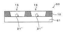
- FIG.1 (a) is a front view which shows an example when the vapor deposition mask concerning 1st Embodiment of this indication is planarly viewed from the metal mask side
- FIG.1 (b) is FIG.1 (a). It is a schematic sectional drawing in the AA part. Note that a portion near the center of the vapor deposition mask in FIG. 1B is omitted.
- a vapor deposition mask 100 includes a resin mask 20 having a plurality of resin mask openings 25 corresponding to a pattern to be vapor-deposited, and a metal mask opening 15.
- the metal mask 10 is an evaporation mask 100 in which the resin mask opening 25 and the metal mask opening 15 are stacked so as to overlap each other.
- the opening shape of the resin mask opening 25 and the metal mask opening 15 is rectangular, but the opening shape is not particularly limited, and the resin mask opening 25 and the metal mask opening 15 are not limited.
- the opening shape may be a diamond shape or a polygonal shape, or may be a shape having a curvature such as a circle or an ellipse.
- the rectangular or polygonal opening shape is a preferable opening shape of the resin mask opening 25 in that the light emission area can be increased as compared with the opening shape having a curvature such as a circle or an ellipse.
- the resin material that is the main material of the resin mask 20 constituting the vapor deposition mask 100 according to the first embodiment shown in FIG. 1 is not limited, and a high-definition resin mask opening 25 can be formed by laser processing or the like. It is preferable to use a lightweight material that has a small rate of dimensional change and moisture absorption over time and heat.
- Such materials include polyimide resin, polyamide resin, polyamideimide resin, polyester resin, polyethylene resin, polyvinyl alcohol resin, polypropylene resin, polycarbonate resin, polystyrene resin, polyacrylonitrile resin, ethylene vinyl acetate copolymer resin, ethylene- Examples thereof include vinyl alcohol copolymer resin, ethylene-methacrylic acid copolymer resin, polyvinyl chloride resin, polyvinylidene chloride resin, cellophane, and ionomer resin.
- a resin material having a moisture absorption rate of 1.0% or less is preferable, and a resin material having both conditions is particularly preferable.
- the thickness of the resin mask 20 is not particularly limited, but in the case of further improving the effect of suppressing the generation of shadows, the thickness of the resin mask 20 is preferably 25 ⁇ m or less, and more preferably less than 10 ⁇ m. Although there is no particular limitation on the preferable range of the lower limit value, when the thickness of the resin mask 20 is less than 3 ⁇ m, defects such as pinholes are likely to occur, and the risk of deformation and the like increases. In particular, by setting the thickness of the resin mask 20 to 3 ⁇ m or more and less than 10 ⁇ m, more preferably 4 ⁇ m or more and 8 ⁇ m or less, it is possible to more effectively prevent the influence of shadows when forming a high-definition pattern exceeding 400 ppi. .
- the resin mask 20 and the metal mask 10 to be described later may be bonded directly or via an adhesive layer, but the resin mask 20 and the metal mask via an adhesive layer. 10 is bonded, it is preferable that the total thickness of the resin mask 20 and the pressure-sensitive adhesive layer is within the range of the preferable thickness.
- the shadow means that a part of the vapor deposition material discharged from the vapor deposition source collides with the inner wall surface of the opening part of the metal mask or the resin mask and does not reach the vapor deposition target, thereby achieving the target vapor deposition. This refers to a phenomenon in which an undeposited portion having a film thickness thinner than the film thickness occurs.
- the cross-sectional shape of the resin mask opening 25 is not particularly limited, and the end faces of the resin mask that form the resin mask opening 25 may be substantially parallel to each other. However, as shown in FIG. It is preferable that the cross-sectional shape of the mask opening 25 is a shape that expands toward the vapor deposition source. In other words, it is preferable to have a tapered surface that expands toward the metal mask 10 side. The taper angle can be set as appropriate in consideration of the thickness of the resin mask 20 and the like.
- the lower bottom tip of the resin mask opening, the straight line connecting the upper base tips of the resin mask opening, and the resin mask The angle formed with the bottom surface, in other words, the cross section in the thickness direction of the inner wall surface constituting the resin mask opening 25, the surface on the side that does not contact the inner mask of the resin mask opening 25 and the metal mask 10 of the resin mask 20 (illustration In this embodiment, the angle formed with the lower surface of the resin mask is preferably in the range of 5 ° to 85 °, more preferably in the range of 15 ° to 75 °, and more preferably 25 ° to 65 °. More preferably, it is within the range of 0 ° or less.
- the end face forming the resin mask opening 25 has a linear shape, but is not limited to this, and has an outwardly convex curved shape, that is, the resin mask opening.
- the entire shape of 25 may be a bowl shape. Further, it may be the opposite, that is, it may have a convex curved shape.
- the arithmetic average height (Sa) of the surface 20 ′ of the resin mask 20 exposed from the metal mask opening 15 is 0.8 ⁇ m or less. It has characteristics. By setting the arithmetic average height (Sa) of the surface 20 ′ to 0.8 ⁇ m or less, it is possible to improve accuracy when the resin mask opening 25 is processed, particularly when laser processing is performed. Further, it is possible to prevent the edge of the resin mask opening 25 from causing a jaggedness or a defect. Furthermore, the arithmetic average height (Sa) of the surface 20 ′ being 0.8 ⁇ m or less means that the thickness of the resin mask 20 is uniform, and thereby the shape of the resin mask opening 25 and The size can be made uniform with higher accuracy.
- the arithmetic average height (Sa) of the surface 20 ′ of the resin mask 20 exposed from the metal mask opening 15 is more preferably 0.1 ⁇ m or less, and particularly preferably 0.08 ⁇ m or less.
- the “arithmetic average height (Sa)” is a parameter obtained by extending the arithmetic average height (Ra) of a line to a surface, and the height of each point with respect to the average surface of the surface to be measured. It is a value calculated by averaging the absolute values of.
- the surface 20 ′ of the resin mask 20 is measured using a shape analysis laser microscope, and can be calculated by a method in accordance with ISO 25178.
- the maximum height (Sz) of the surface 20 ′ of the resin mask 20 exposed from the metal mask opening 15 is 2.5 ⁇ m or less. preferable.
- the arithmetic average height (Sa) is 0.8 ⁇ m or less and the maximum height (Sz) is 2.5 ⁇ m or less, the thickness of the resin mask 20 becomes even more uniform, thereby the resin mask opening.
- the shape and size of 25 can be made uniform with higher accuracy.
- the maximum height (Sz) of the surface 20 ′ of the resin mask 20 exposed from the metal mask opening 15 is more preferably 2.0 ⁇ m or less, and particularly preferably 1.5 ⁇ m or less.
- the “maximum height (Sz)” is a parameter obtained by extending the maximum height Rz of the line to the surface, and is a value representing the distance from the highest point to the lowest point on the surface to be measured. .
- the surface 20 ′ of the resin mask 20 is measured using a shape analysis laser microscope, and can be calculated by a method according to ISO 25178.
- a metal mask 10 is laminated on one surface of the resin mask 20.
- the metal mask 10 is made of metal, and has a metal mask opening 15 extending in the vertical direction or the horizontal direction.
- the arrangement example of the metal mask openings is not particularly limited, and the metal mask openings extending in the vertical direction and the horizontal direction may be arranged in a plurality of rows in the vertical direction and the horizontal direction, and the metal mask openings extending in the vertical direction.
- the portions may be arranged in a plurality of rows in the horizontal direction, and the metal mask openings extending in the horizontal direction may be arranged in a plurality of rows in the vertical direction. Further, only one row may be arranged in the vertical direction or the horizontal direction.
- vertical direction and lateral direction refer to the vertical and horizontal directions in the drawing, and are any of the longitudinal direction and the width direction of the vapor deposition mask, resin mask, and metal mask. May be.
- the longitudinal direction of the vapor deposition mask, the resin mask, and the metal mask may be “vertical direction”
- the width direction may be “vertical direction”.
- shape of the vapor deposition mask when viewed in plan is a rectangular shape is described as an example, but other shapes, for example, a circular shape, a polygonal shape such as a rhombus shape, etc. It is good.
- the longitudinal direction, the radial direction, or an arbitrary direction of the diagonal line is defined as a “longitudinal direction”, and a direction orthogonal to the “longitudinal direction” is referred to as a “width direction (sometimes referred to as a short direction)”. do it.
- the material of the metal mask 10 is not particularly limited, and any conventionally known material can be appropriately selected and used in the field of the evaporation mask, and examples thereof include metal materials such as stainless steel, iron-nickel alloy, and aluminum alloy. . Among them, an invar material that is an iron-nickel alloy can be suitably used because it is less deformed by heat.
- the thickness of the metal mask 10 is not particularly limited, it is preferably 100 ⁇ m or less, more preferably 50 ⁇ m or less, and more preferably 35 ⁇ m or less in order to more effectively prevent the occurrence of shadows. Particularly preferred. When the thickness is less than 5 ⁇ m, the risk of breakage and deformation increases and handling tends to be difficult.
- the opening shape when the metal mask opening 15 is viewed in plan is a rectangular shape, but the opening shape is not particularly limited, and the opening of the metal mask opening 15 is not limited.
- the shape may be any shape such as a trapezoidal shape or a circular shape.
- the cross-sectional shape of the metal mask opening 15 formed in the metal mask 10 is not particularly limited, but may be a shape having a spread toward the vapor deposition source as shown in FIG. preferable. More specifically, the angle formed by the straight line connecting the lower bottom tip of the metal mask opening and the upper bottom tip of the metal mask opening 15 and the bottom surface of the metal mask 10, in other words, the metal mask opening.
- the angle formed between the inner wall surface of the metal mask opening 15 and the surface of the metal mask 10 on the side in contact with the resin mask 20 is It is preferably in the range of 5 ° to 85 °, more preferably in the range of 15 ° to 80 °, and still more preferably in the range of 25 ° to 65 °. In particular, within this range, an angle smaller than the vapor deposition angle of the vapor deposition machine to be used is preferable.
- the vapor deposition mask 100 according to the first embodiment of the present disclosure may be a vapor deposition mask with a frame by fixing the vapor deposition mask 100 to the frame.
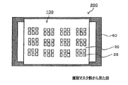
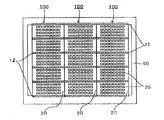
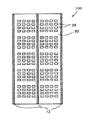
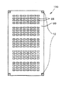
- FIG. 2 is a front view showing an example of a vapor deposition mask with a frame
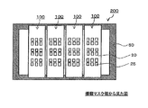
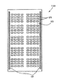
- FIG. 3 is a front view showing an example of a vapor deposition mask with a frame
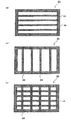
- FIGS. 4A to 4C are embodiments of the present disclosure. It is a front view showing an example of a frame concerning.
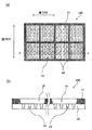
- the frame-equipped vapor deposition mask 200 may be one in which one vapor deposition mask 100 is fixed to the frame 60, and as shown in FIG. 3, the frame 60 has a plurality of vapor deposition masks 100. May be fixed.
- the frame 60 is a substantially rectangular frame member, and has an opening for exposing the resin mask opening 25 provided in the resin mask 20 of the vapor deposition mask 100 to be finally fixed to the vapor deposition source side.
- the frame material include a metal material, a glass material, and a ceramic material.
- the thickness of the frame is not particularly limited, but is preferably in the range of 10 mm to 30 mm from the viewpoint of rigidity and the like.
- the width between the inner peripheral end face of the opening of the frame and the outer peripheral end face of the frame is not particularly limited as long as the frame and the metal mask of the vapor deposition mask can be fixed, for example, 10 mm or more and 70 mm or less. Within range.
- a frame 60 in which a reinforcing frame 65 or the like is provided in the opening area of the frame may be used.
- the opening of the frame 60 may be divided by a reinforcing frame or the like.
- the frame 60 and the vapor deposition mask 100 can be fixed using the reinforcing frame 65.
- the vapor deposition mask 100 can be fixed to the frame 60 even at a position where the reinforcing frame and the vapor deposition mask overlap. it can.
- the frame 60 and the vapor deposition mask 100 can be fixed using spot welding, adhesive, screwing, or other methods for fixing with a laser beam or the like.
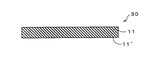
- FIG. 5 is a cross-sectional view showing an example of a vapor deposition mask preparation according to the first embodiment of the present disclosure.
- a first vapor deposition mask preparation 30 shown in FIG. 5 is prepared.
- the first vapor deposition mask preparation 30 is a metal plate 11 and is characterized in that the arithmetic average height (Sa) of its surface 11 ′ (lower surface in FIG. 5) is 0.8 ⁇ m or less. is doing.
- a resin layer is laminated on the surface 11 ′ of the metal plate 11 constituting the vapor deposition mask preparation 30, and the metal plate 11 is processed to form a metal mask.
- the resin layer is processed into a resin mask. In this case, the roughness of the surface of the resin mask finally exposed from the metal mask opening of the metal mask is copied from the roughness of the surface of the metal mask (metal plate 11) in contact with the resin mask.
- the arithmetic average height (Sa) of the surface 11 ′ of the metal plate 11 constituting the surface is 11 ⁇ m or less.
- the arithmetic average height (Sa) of the surface of the resin layer laminated on the substrate can also be 0.8 ⁇ m or less.
- the material, shape, and thickness of the metal plate 11 are the same as those of the above-described metal mask, and thus description thereof is omitted here.
- the maximum height (Sz) of the surface is preferably 2.5 ⁇ m or less, and particularly preferably 2.0 ⁇ m or less.
- the method of setting the arithmetic average height (Sa) of the surface 11 ′ of the metal plate 11 to 0.8 ⁇ m or less, and the method of setting the maximum height (Sz) to 2.5 ⁇ m or less are particularly limited. However, it can be appropriately selected from conventionally known various methods.
- a metal plate having a surface arithmetic average height (Sa) of 0.8 ⁇ m or less and a maximum height (Sz) of 2.5 ⁇ m or less will be described with reference to FIGS. 8 and 9. It is shown below. Specifically, an example in which the metal plate is made of a rolled material of an iron alloy containing nickel will be described.
- This rolled material has a thickness of 35 ⁇ m or less. Further, the total content of nickel and cobalt in the rolled material is 30% by mass or more and 38% by mass or less.
- each raw material is prepared so that the ratio of iron to the total raw material and the ratio of nickel are about 64 wt% and about 36 wt%, respectively.
- a melting step of melting each raw material in a melting furnace is performed.
- each raw material is melted and mixed using gas discharge such as arc discharge.
- gas discharge such as arc discharge.
- a base material for the metal plate can be obtained.
- dissolution is set according to a raw material, it is 1500 degreeC or more, for example.
- the melting step may include a step of introducing aluminum, manganese, silicon, or the like into a melting furnace for deoxidation, dehydration, denitrification, or the like. Moreover, you may implement a melt
- inert gas such as argon gas
- a grinding step of scraping the surface of the base material After taking out the base material from the melting furnace, a grinding step of scraping the surface of the base material may be performed. Thereby, the oxide film such as scale can be removed.
- the specific grinding method is not particularly limited, but the so-called grinding method in which the grinding wheel is rotated to cut the surface of the base material, or the so-called indentation method in which the base material is pushed into a cutting tool and the surface of the base material is shaved. Etc. can be adopted.
- the grinding step may be performed so that the thickness of the base material is uniform.
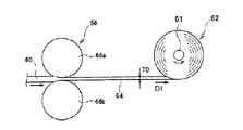
- the wound body 62 may be formed by winding a metal plate 64 around a core 61.
- FIG. 8 only shows the outline of a rolling process, and the specific structure and procedure for implementing a rolling process are not specifically limited.
- the rolling process includes a hot rolling process in which the base material is processed at a temperature equal to or higher than the temperature at which the crystal arrangement of the iron alloy constituting the base material 60 is changed, and a base material at a temperature lower than the temperature at which the crystal arrangement of the iron alloy is changed. It may include a cold rolling process for processing.
- the direction at the time of passing the base material 60 and the metal plate 64 between a pair of rolling rolls 66a and 66b is not restricted to one direction. For example, in FIGS.
- the base material 60 and the metal plate 64 may be gradually rolled.
- the surface roughness of the metal plate 64 can be adjusted by adjusting the diameters of the rolling rolls 66 a and 66 b that are in contact with the base material 60.
- the surface roughness of the metal plate can be reduced by reducing the diameter of the rolling rolls 66a and 66b.
- the pressure of the rolling actuator may be adjusted in order to adjust the shape of the metal plate 64.
- the shape of the backup roll may be adjusted as appropriate, and the position of the backup roll may be adjusted as appropriate in the plate width direction.
- you may adjust a rolling speed, ie, the conveyance speed of a base material.
- a coolant such as kerosene may be supplied between the base material 60 and the rolling rolls 66a and 66b. Thereby, the temperature of the base material can be controlled.
- the analysis process which analyzes the quality and characteristic of the base material 60 or the metal plate 64 before and after a rolling process, or during a rolling process.
- the composition may be analyzed by irradiating the base material 60 or the metal plate 64 with fluorescent X-rays.
- the thermal expansion amount of the base material 60 or the metal plate 64 may be measured by thermomechanical analysis (TMA: Thermomechanical Analysis).
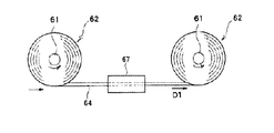
- the metal plate 64 may be annealed using an annealing device 67 as shown in FIG.
- the annealing step may be performed while pulling the metal plate 64 in the transport direction (longitudinal direction). That is, the annealing step may be performed as continuous annealing while being conveyed, not so-called batch-type annealing. In this case, it is preferable to set the temperature and the conveyance speed so as to suppress deformation such as bending of the metal plate 64.
- the metal plate 64 from which residual strain has been removed to some extent can be obtained.
- the present invention is not limited to this, and the metal plate 64 is moved in the vertical direction or the like during the annealing step. You may convey in another direction.
- the conditions for the annealing step are appropriately set according to the thickness of the metal plate 64, the rolling reduction, and the like.
- the annealing step is performed within a range of 500 ° C. to 600 ° C. for 30 seconds to 90 seconds.
- the number of seconds represents the time required for the metal plate 64 to pass through the space adjusted to a predetermined temperature in the annealing device 67.
- the temperature of the annealing process may be set so that the metal plate 64 does not soften.
- the above-described annealing step is performed in a non-reducing atmosphere or an inert gas atmosphere.
- the non-reducing atmosphere is an atmosphere that does not contain a reducing gas such as hydrogen. “Does not contain reducing gas” means that the concentration of reducing gas such as hydrogen is 10% or less.
- the inert gas atmosphere is an atmosphere in which the concentration of an inert gas such as argon gas, helium gas, or nitrogen gas is 90% or more.
- the annealing device 67 may have a mechanism for monitoring the concentration of the inert gas and a mechanism for adjusting the concentration of the inert gas.
- a cleaning process for cleaning the metal plate 64 may be performed before the annealing process. Thereby, it can suppress that a foreign material adheres to the surface of the metal plate 64 in the annealing process.
- As the cleaning liquid for cleaning for example, a hydrocarbon-based liquid can be used.
- FIG. 9 shows an example in which the annealing process is performed while pulling the metal plate 64 in the longitudinal direction.
- the present invention is not limited to this, and the annealing process is performed by winding the metal plate 64 around the core 61. You may carry out in the state made. That is, batch-type annealing may be performed.
- the metal plate 64 may be wrinkled with a warp corresponding to the winding diameter of the wound body 62. Therefore, depending on the winding diameter of the wound body 62 and the material constituting the base material 60, it is advantageous to perform the annealing step while pulling the metal plate 64 in the longitudinal direction.
- the long metal plate 64 having a predetermined thickness may be produced by repeating at least two of the rolling process, the annealing process, and the slit process a plurality of times.
- a metal plate having a surface arithmetic average height (Sa) of 0.8 ⁇ m or less and a maximum height (Sz) of 2.5 ⁇ m or less can be produced.
- FIG. 6 is a cross-sectional view showing an example of a deposition mask preparation according to the first embodiment of the present disclosure different from FIG.
- the resin layer 21 is laminated on the surface 11 ′ of the metal plate 11 constituting the vapor deposition mask preparation 30 illustrated in FIG. 5.
- the lamination method of the resin layer 21 is not particularly limited, and a resin layer that finally becomes a resin mask can be formed by a conventionally known coating method or the like.
- a resin layer coating liquid prepared by dispersing or dissolving the resin mask material described above and any components added as necessary in an appropriate solvent is prepared, and this is applied to the surface 11 ′ of the metal plate 11.
- it can be set as the resin layer 21 by coating and drying using a conventionally known coating means.
- the arithmetic average height (Sa) of the surface 21 ′ in contact with the metal plate 11 in the resin layer 21 constituting the vapor deposition mask preparation 40 obtained by such a method is the surface 11 ′ in contact with the resin layer 21 in the metal plate 11. Since it is the same as the arithmetic average height (Sa), it is naturally 0.8 ⁇ m or less.
- the resin layer 21 is formed on a surface having an arithmetic average height (Sa) of 0.8 ⁇ m or less, the resin layer 21 is peeled off from the other surface, and the arithmetic operation in the resin layer 21 is performed.
- the vapor deposition mask preparation 40 may be formed by bonding a surface having an average height (Sa) of 0.8 ⁇ m or less to the metal plate 11.
- examples of the surface having an arithmetic average height (Sa) of 0.8 ⁇ m or less include non-alkali glass (Nippon Electric Glass Co., Ltd., OA-10G).
- FIG. 7 is a cross-sectional view showing an example of a deposition mask preparation according to the first embodiment of the present disclosure different from FIGS. 5 and 6.
- the metal mask 10 is formed by processing the metal mask opening 15 in the metal plate 11 constituting the vapor deposition mask preparation 40 shown in FIG. Is formed.
- the processing method of the metal mask opening 15 is not particularly limited, and can be appropriately selected from conventionally known processing methods.
- a masking member for example, a resist material, and a predetermined portion is exposed and developed to form a resist pattern that leaves the position where the metal mask opening 15 is finally formed.
- the resist material used as the masking member those having good processability and desired resolution are preferable.
- etching is performed from the side not in contact with the resin layer 21 by an etching method using this resist pattern as an etching resistant mask.
- the resist pattern is removed by washing.
- the vapor deposition mask preparation 50 in which the metal mask 10 provided with the metal mask opening 15 on one surface of the resin layer 21 is laminated is obtained.
- the resin layer 21 has etching resistance with respect to the etching material of the metal plate 11, it is not necessary to mask the surface of the resin layer 21, but the resin layer 21 is resistant to the etching material of the metal plate 11.
- it does not have, it is necessary to coat the masking member on the surface of the resin layer 21.
- the resist material is mainly described as the masking member. However, instead of coating the resist material, a dry film resist may be laminated and the same patterning may be performed.
- the arithmetic average height (Sa) of the surface 21 ′ of the resin layer 21 exposed from the metal mask opening 15 in the vapor deposition mask preparation 50 obtained by the manufacturing method is 0.8 ⁇ m or less, and in addition, the metal plate 11 has a maximum height (Sz) of 2.5 ⁇ m or less, the maximum height (Sz) of the surface 21 ′ of the resin layer 21 is also 2.5 ⁇ m or less.
- the vapor deposition mask preparation 30 shown in FIG. 5 that is, the vapor deposition mask preparation in which the arithmetic average height (Sa) of the surface 11 ′ of the metal plate 11 is not less than 0.8 ⁇ m
- the arithmetic average height (Sa) of the surface of the resin layer exposed from the opening of the metal mask may not be 0.8 ⁇ m or less.
- the arithmetic average height (Sa) of the surface may be 0.8 ⁇ m or less by processing the surface of the resin layer exposed from the opening of the metal mask.
- a processing method of the resin layer surface it can select suitably from conventionally well-known various methods.
- the vapor deposition mask preparation whose arithmetic mean height (Sa) of surface 11 'of the metal plate 11 is not 0.8 micrometer or less, before forming the resin layer 21 on the surface 11' of the said metal plate 11
- a planarization layer may be formed on the surface 11 ′.
- the material for forming the planarizing layer is not particularly limited, and various resins similar to the resin layer 21 can be used, for example.
- the resin layer 21 is formed not on the surface of the metal plate but on another surface, more specifically on the surface having an arithmetic average height (Sa) of 0.8 ⁇ m or less.
- the metal layer may be formed by peeling the resin layer 21 from above and depositing a metal in a predetermined pattern on a surface having an arithmetic average height (Sa) of the resin layer 21 of 0.8 ⁇ m or less.
- the above alkali-free glass or the like can be used as the surface having an arithmetic average height (Sa) of 0.8 ⁇ m or less.
- As a method for depositing the metal various plating methods can be used.
- the metal is deposited on the surface of the resin layer 21 having an arithmetic average height (Sa) of 0.8 ⁇ m or less by using an electroless plating method.
- a metal mask may be formed by using an electrolytic plating method with this as an underlayer.
- an alkali-free glass having an arithmetic average height (Sa) of the surface of 0.8 ⁇ m or less is prepared, and the resin layer 21 is formed on the surface, A metal mask may be formed on the resin layer 21 in this state, and then the resin layer 21 with the metal mask may be peeled from the alkali-free glass. Furthermore, without peeling the resin layer 21 with the metal mask from the alkali-free glass, it is fixed to the frame as it is, and a resin mask opening 25 is formed in the resin layer 21 using a laser processing method described later, Finally, the inorganic alkali glass may be peeled off.
- Sa arithmetic average height
- the resin mask opening 25 is processed in the resin layer 21 constituting the vapor deposition mask preparation 50 shown in FIG.
- the vapor deposition mask 100 shown is manufactured.
- the vapor deposition mask preparation 50 is penetrated through the resin layer 21 using a laser processing method, precision press processing, photolithographic processing, or the like to form a vapor deposition pattern on the resin layer 21.
- the vapor deposition mask 100 according to the actual embodiment of the present disclosure is obtained.
- the arithmetic average height (Sa) of the surface 21 ′ of the resin layer 21 to which the laser processing method is applied is 0.8 ⁇ m or less, Furthermore, since the maximum height (Sz) is 2.5 ⁇ m or less and the smoothness is high, it is suitable for the laser processing method.
- the method for fixing the vapor deposition mask preparation 50 and the frame is not particularly limited, and the mask can be fixed using spot welding, adhesive, screwing, or other methods for fixing with a laser beam or the like.
- the laser processing apparatus includes an XY stage, a laser light source, a coupling optical system, a beam shaping mask, an image forming lens, an objective lens, and a laser beam source, which are located above the XY stage from upstream to downstream in the laser light traveling direction.
- the lens is provided in this order.
- the XY stage is configured to place a mask member on the upper surface and move in the XY direction in a plane parallel to the XY plane.
- the XY stage is controlled by a control device and moves stepwise by a movement amount input and stored in advance. It is like that.
- the laser light source is, for example, an excimer laser with a wavelength of 400 nm or less, for example, an excimer laser with a KrF of 248 nm, or a YAG laser that emits laser light with a third or fourth harmonic of 1064 nm.
- the coupling optical system includes a beam expander that expands the laser beam emitted from the laser light source, a photo integrator and a condenser lens that irradiates a beam shaping mask described later with a uniform luminance distribution of the laser beam. It is a waste.
- the beam shaping mask is formed by emitting laser light applied to a mask member into a laser beam having a cross-sectional shape similar to the opening pattern to be formed.
- the imaging lens is a condensing lens that projects a plurality of light transmission windows formed in a beam shaping mask in cooperation with an objective lens, which will be described later, onto a resin layer at a predetermined magnification.
- the objective lens projects a plurality of light-transmitting windows formed on the beam shaping mask in cooperation with the imaging lens at a predetermined magnification on the resin layer.
- the XY stage moves and the objective lens is positioned at the laser processing start position of the frame-equipped vapor deposition mask preparation.
- the optical unit of the laser processing apparatus is raised in the Z-axis direction by a predetermined distance along the optical axis of the objective lens, and the imaging position of the objective lens is set to the resin layer and the XY stage of the deposition mask preparation body with a frame. Position it at the interface.
- the laser light source is activated to generate a pulse oscillation, and a plurality of shot laser beams are emitted.
- the emitted laser beam is expanded by a coupling optical system, and is applied to the beam shaping mask as laser light having a uniform intensity distribution.
- the laser light applied to the beam shaping mask is transmitted through a plurality of light transmission windows of the beam shaping mask, so that the cross-sectional shape is shaped to be similar to the shape of the opening pattern, and becomes a plurality of laser lights.
- the light is condensed on the resin layer by the objective lens.
- the XY stage is stepped by a predetermined distance in the X or Y axis direction, the second unit region, the third unit region, and so on.
- a plurality of opening patterns are laser processed in order in each unit region.
- a plurality of opening patterns are laser processed at predetermined positions on the resin layer, and a resin mask is formed.
- FIG. 10A is a front view showing an example when the vapor deposition mask according to the second embodiment of the present disclosure is viewed from the metal mask side
- FIG. 10B is a front view of FIG. It is a schematic sectional drawing in the AA part. Note that a portion near the center of the vapor deposition mask in FIG. 10B is omitted.
- the vapor deposition mask 100 according to the second embodiment of the present disclosure is similar to the vapor deposition mask 100 according to the first embodiment of the present disclosure.
- a vapor deposition mask 100 in which a resin mask 20 having an opening 25 and a metal mask 10 having a metal mask opening 15 are laminated so that the resin mask opening 25 and the metal mask opening 15 overlap each other. is there.
- Such a vapor deposition mask 100 according to the second embodiment of the present disclosure is a surface 20 ′′ of the resin mask 20 on the side opposite to the surface on the metal mask 10 side, that is, the side not in contact with the metal mask 10. It is characterized in that the arithmetic average height (Sa) of the surface 20 ′′ is 0.5 ⁇ m or less. By setting the arithmetic average height (Sa) of the surface 20 ′′ to 0.5 ⁇ m or less, a desired pattern is deposited on the deposition target using the deposition mask 100 according to the second embodiment of the present disclosure.
- the arithmetic average height (Sa) of the surface 20 ′′ being 0.5 ⁇ m or less means that the thickness of the resin mask 20 is uniform, and thereby the shape of the resin mask opening 25 is formed. And the size can be made uniform with higher accuracy.
- the arithmetic average height (Sa) of the surface 20 ′′ of the resin mask 20 opposite to the surface on the metal mask 10 side, that is, 20 ′′ on the side not in contact with the metal mask 10, is 0.1 ⁇ m or less. It is more preferable that it is 0.05 ⁇ m or less.
- the surface 20 ′′ of the resin mask 20 opposite to the surface on the metal mask 10 side that is, the side not in contact with the metal mask 10 is provided.
- the maximum height (Sz) of the surface 20 ′′ is preferably 2.0 ⁇ m or less. Since the arithmetic average height (Sa) is 0.5 ⁇ m or less and the maximum height (Sz) is 2.0 ⁇ m or less, the surface of the resin mask 20 opposite to the surface on the metal mask 10 side The adhesion between 20 ′′ and the deposition object can be further improved.
- the maximum height (Sz) of the surface 20 ′ of the resin mask 20 on the side not in contact with the metal mask 10 is more preferably 1.0 ⁇ m or less, and particularly preferably 0.8 ⁇ m or less.
- maximum height (Sz) is the same as that of the vapor deposition mask 100 according to the first embodiment, the description thereof is omitted here.
- Metal mask As shown in FIG. 1B, a metal mask 10 is laminated on one surface of the resin mask 20.
- the details of the metal mask 10, specifically, the arrangement of the metal mask openings 15, the material and thickness of the metal mask 10, the opening shape and the cross-sectional shape of the metal mask opening 15, are described in the first embodiment. Since it is the same as the vapor deposition mask 100 concerning a form, description here is abbreviate
- the vapor deposition mask 100 according to the second embodiment of the present disclosure may also be a vapor deposition mask with a frame by being fixed to the frame in the same manner as the vapor deposition mask 100 according to the first embodiment.
- An example of the frame-equipped vapor deposition mask and the frame using the vapor deposition mask 100 according to the second embodiment of the present disclosure are the same as those of the vapor deposition mask 100 according to the first embodiment, and thus description thereof is omitted here.
- FIG. 11 is a cross-sectional view showing an example of a metal plate.
- a metal plate 11 shown in FIG. 11 is prepared.
- the arithmetic average height (Sa) of the surface 11 ′′ (the lower surface in FIG. 5) of the metal plate 11 is 0.5 ⁇ m or less.
- the resin layer when a resin layer is laminated on the surface 11 ′′ of the metal plate 11, the resin layer follows the unevenness of the surface 11 ′′ of the metal plate 11, and the surface of the resin layer on the metal plate 11 side is The unevenness of the surface 11 ′′ of the metal plate 11 is also reflected on the opposite surface, that is, the surface not in contact with the metal plate 11. This phenomenon becomes more prominent as the resin layer is thinner. Therefore, by using the metal plate 11 having an arithmetic average height (Sa) of the surface 11 ′′ of 0.5 ⁇ m or less, the surface of the resin layer laminated thereafter is the surface opposite to the surface on the metal plate 11 side. That is, the arithmetic average height (Sa) on the surface not in contact with the metal plate 11 can also be 0.5 ⁇ m or less.
- the material, shape, and thickness of the metal plate 11 are the same as those of the above-described metal mask, and thus description thereof is omitted here.
- the maximum height (Sz) of the surface is preferably 2.0 ⁇ m or less.
- the method of setting the arithmetic average height (Sa) of the surface 11 ′′ of the metal plate 11 to 0.5 ⁇ m or less, and the method of setting the maximum height (Sz) to 2.0 ⁇ m or less are particularly limited. It is not carried out, and it can select suitably from conventionally well-known various methods. Specifically, the “rolled material manufacturing method” described in the vapor deposition mask 100 according to the first embodiment can be used.
- FIG. 12 is a cross-sectional view illustrating an example of a deposition mask preparation according to the second embodiment of the present disclosure.
- the resin layer 21 is laminated on the surface 11 ′′ of the metal plate 11 shown in FIG.
- the same method as the method for manufacturing the vapor deposition mask according to the first embodiment can be used.
- the arithmetic average height (Sa) of the surface 21 ′′ on the side not in contact with the metal plate 11 in the resin layer 21 constituting the vapor deposition mask preparation 40 is the surface 11 ′ in contact with the resin layer 21 in the metal plate 11. It follows the arithmetic average height (Sa) of 'and is 0.5 ⁇ m or less.
- the resin layer 21 on the side not in contact with the metal plate 11 is used.
- the arithmetic average height (Sa) of the surface 21 ′′ may not be 0.5 ⁇ m or less.
- the arithmetic average height (Sa) of the surface 21 ′′ may be set to 0.5 ⁇ m or less by processing the surface 21 ′′ of the resin layer 21.
- a processing method of the resin layer surface it can select suitably from conventionally well-known various methods.
- the arithmetic average height (Sa) of the surface 11 ′′ of the metal plate 11 is not 0.5 ⁇ m or less, in the stage before the resin layer 21 is formed on the surface 11 ′′ of the metal plate 11, A planarizing layer may be formed on the surface 11 ′.
- the material for forming the planarizing layer is not particularly limited, and various resins similar to the resin layer 21 can be used, for example.
- the metal plate 11 when using the metal plate 11 as a vapor deposition mask preparation whose surface 11 '' arithmetic mean height (Sa) is not 0.5 micrometer or less, it is not on the surface of the said metal plate but on another surface. More specifically, the resin layer 21 is formed on a surface having an arithmetic average height (Sa) of 0.5 ⁇ m or less, the resin layer 21 is peeled off from the other surface, and the resin layer 21 is made of metal. You may form the vapor deposition mask preparation 40 by bonding with the board 11.
- examples of the surface having an arithmetic average height (Sa) of 0.5 ⁇ m or less include non-alkali glass (Nippon Electric Glass Co., Ltd., OA-10G).
- FIG. 13 is a cross-sectional view showing an example of a deposition mask preparation according to the second embodiment of the present disclosure different from FIGS. 11 and 12.
- the metal mask 10 is formed by processing the metal mask opening 15 in the metal plate 11 constituting the vapor deposition mask preparation 40 shown in FIG. Is formed.
- the processing method of the metal mask opening 15 is the same as the manufacturing method of the vapor deposition mask according to the first embodiment, and a description thereof is omitted here.
- the arithmetic average height (Sa) of the surface 21 ′′ on the side not in contact with the metal mask in the resin layer 21 is 0.5 ⁇ m.
- the maximum height (Sz) of the surface of the metal plate 11 is 2.0 ⁇ m or less
- the maximum height (Sz) of the surface 21 ′ of the resin layer 21 is also 2.0 ⁇ m or less. It is.
- the resin mask opening 25 is processed in the resin layer 21 constituting the vapor deposition mask preparation 50 illustrated in FIG.
- the vapor deposition mask 100 shown is manufactured.
- the method for forming the resin mask opening 25 is the same as the method for manufacturing the vapor deposition mask according to the first embodiment, and a description thereof is omitted here.
- a vapor deposition mask according to a third embodiment of the present disclosure is a vapor deposition mask including a resin mask provided with a resin mask opening corresponding to a pattern to be vapor-deposited, and has an arithmetic average height on one surface of the resin mask.
- the thickness (Sa) is 0.8 ⁇ m or less.
- Each of the vapor deposition masks according to the first and second embodiments has a laminated structure in which a metal mask and a resin mask are laminated, but is not limited to this, and an arithmetic average of one surface thereof What is necessary is just a vapor deposition mask containing the resin mask whose height (Sa) is 0.8 micrometer or less.
- a resin mask having an arithmetic average height (Sa) on one side of 0.8 ⁇ m or less may be used as a vapor deposition mask. Since the details of the resin mask in this case are the same as those of the resin mask constituting the vapor deposition mask according to the first and second embodiments, description thereof is omitted here.
- the arithmetic mean height (Sa) of the surface is 0.8 micrometer or less alkali free
- a resin layer may be used as a resin mask by preparing glass or the like, forming a resin layer on the surface, and forming a resin mask opening in the resin layer using a laser processing method or the like.
- the arithmetic mean height (Sa) in a resin mask is 0.
- the surface of 8 ⁇ m or less may be used toward the deposition source side, and conversely, that is, the surface having an arithmetic average height (Sa) of 0.8 ⁇ m or less may be used toward the deposition object side.
- the vapor deposition mask according to the third embodiment of the present disclosure is more accurately formed on one surface of the resin mask 20 provided with the resin mask opening 25.
- the metal layer 12 may be partially provided on one surface of the resin mask 20 provided with the opening 25 and in a portion where the resin mask opening 25 is not provided. According to such a vapor deposition mask, when the vapor deposition mask is fixed to the frame, the stress that can be generated in the resin mask 20 can be appropriately released, and as a result, deformation such as expansion and contraction is effectively suppressed. be able to.
- the metal layer 12 may be provided on a surface having an arithmetic average height (Sa) of the resin mask 20 of 0.8 ⁇ m or less, and the opposite surface, that is, the arithmetic average height (Sa). May be provided on the surface opposite to the surface of 0.8 ⁇ m or less.
- the arithmetic average height (Sa) of the surface on which the metal layer 12 is not provided is preferably 0.5 ⁇ m or less.
- the position where the metal layer 12 is provided and the planar shape when the metal layer 12 is viewed in plan are not particularly limited. That is, the planar shape of the metal layer 12 can be appropriately designed according to the position where the metal layer is provided.
- the resin mask 20 when the vapor deposition mask 100 according to the third embodiment is viewed from the side where the metal layer 12 is provided, the resin mask 20 has a long side and a short side.
- the metal layer 12 may have a band shape along the side of the resin mask.
- the metal layer 12 may be arranged in parallel with the short side of the resin mask 20 while forming a band shape having the same length as the short side.
- the resin mask 20 when the vapor deposition mask 100 according to the third embodiment is viewed from the side where the metal layer 12 is provided, the resin mask 20 has a rectangular shape having a long side and a short side.
- the shape of the metal layer 12 may be a strip shape having the same length as the long side, and may be arranged in parallel with the long side of the resin mask 20.
- the shape of the metal layer may be a band shape having a predetermined angle with respect to the long side of the resin mask.
- the quadrilateral is not limited to a rectangle, and may be, for example, a trapezoid, a parallelogram, or another quadrilateral.
- the shape of the resin mask 20 in plan view may be a shape other than the quadrilateral.
- the shape and arrangement of the metal layer 12 described in the present specification can be applied as appropriate to the resin mask 20 having a shape other than the quadrangular shape when the resin mask 20 is planarized.
- each band-shaped metal layers 12 are arranged in parallel with the short sides of the resin mask 20, and in the form shown in FIG. 20, three bands are parallel to the long sides of the resin mask 20.
- the shape of the metal layer 12 is arranged, the number of the metal layers 12 arranged is not limited. For example, although not shown, only one metal layer 12 of the plurality of metal layers 12 is arranged. It is good also as the arrangement
- the band-shaped metal layer 12 having the same length as the short side may be disposed only in the vicinity of the upper side and the lower side of the resin mask 20, and as shown in FIG.
- the band-shaped metal layer 12 having the same length as the long side may be disposed only on the left side of the mask 20 and in the vicinity of the right side.
- the metal layer 12 located in the vicinity of the upper side and the lower side of the resin mask, or in the vicinity of the right side and the left side of the resin mask is arranged at a position overlapping the periphery of the resin mask 20.
- the metal layer 12 may be disposed only on the peripheral edge of the resin mask 20.
- the peripheral part of the resin mask 20 as used in this specification means the area
- the metal layer 12 may be arranged only in the vicinity of one or both of the upper side and the lower side of the resin mask in the peripheral part of the resin mask 20. In this case, the metal layer 12 may be disposed so as to overlap the periphery of the resin mask.
- a metal layer having a length different from the long side or the short side of the resin mask 20 is used instead of the strip-shaped metal layer 12 having the same length as the long side or the short side of the resin mask 20 .
- One may be arranged in parallel with 20 long sides or short sides, or a plurality of them may be arranged.
- One or a plurality of band-shaped metal layers 12 may be arranged in random directions.
- the strip-shaped metal layer 12 having a length shorter than the right side and the left side, that is, the long side of the resin mask 20 is arranged at positions separated from the peripheral edges of the right side and the left side of the resin mask 20.
- the region where the metal layer 12 is disposed in FIG. 22 may be a peripheral portion of the resin mask 20 or a non-peripheral portion.
- region which straddles a peripheral part and a non-peripheral part may be sufficient.
- the non-peripheral part of the resin mask 20 as used in this specification means the whole area
- the band-shaped metal layer 12 arranged in parallel to the long side of the resin mask 20 is divided into a plurality of pieces in the length direction and five pieces in FIG. Also good.
- FIG. 15 is a front view showing an example when the deposition mask of the third embodiment is viewed from the metal layer 12 side.
- the metal layer 12 is not necessarily required to be positioned on the peripheral edge of the resin mask 20.
- FIG. 15 shows an example in which the metal layer 12 is positioned only on the non-peripheral portion of the resin mask 20. Further, the metal layer 12 may be disposed on the peripheral edge and the non-peripheral edge of the resin mask 20.
- the metal layer 12 is used only for fixing to the frame by disposing the metal layer 12 on the non-peripheral portion of the resin mask 20, specifically, at a position that does not overlap the frame in the resin mask 20. Instead, deformation such as elongation or shrinkage that can occur in the resin mask 20 can be effectively suppressed.
- the resin mask 20 is fixed when the vapor deposition mask is fixed to the frame as compared to the case where the metal layer 12 surrounds the periphery of the opening 25 formed in the resin mask 20. It is possible to appropriately release the stress that can be generated in the film, and as a result, it is possible to effectively suppress deformation such as expansion and contraction.
- the dotted line shown in FIG. 15 indicates an area of “one screen”.
- the metal layer 12 may be disposed between “one screen” and “one screen”.
- FIG. 16 is a front view showing an example when the vapor deposition mask according to the third embodiment is viewed in plan view from the side on which the metal layer is formed.
- the metal layer 12 does not necessarily have a strip shape, and may be arranged so as to be scattered on the resin mask 20. Further, as shown in FIG. It may be arranged only at the four corners of the resin mask 20. In such a case, the metal layer 12 shown in FIG. 16 and FIG. 24 is a square, but is not limited to this, and is not limited to this, but a rectangle, a triangle, a quadrilateral or more, a circle, an ellipse, a semicircle, a donut. Any shape such as a shape, an alphabetic “C” shape, a “T” shape, a “cross” shape or a “star” shape can be employed.
- a vapor deposition mask 100 of a preferred form has a band-shaped metal layer 12 disposed on a resin mask 20.
- the band-shaped metal layer 12 is disposed along the transport direction of the vapor deposition mask 100 during vapor deposition.
- the band-shaped metal layer 12 is disposed on the resin mask 10 along a direction perpendicular to the linear source (vapor deposition source) during vapor deposition. .
- the band-shaped metal layer 12 is positioned along the transport direction as shown in FIGS.
- the vapor deposition mask 100 is preferable. According to the vapor deposition mask 100 of this form, it can suppress more effectively that a dimensional fluctuation and a position fluctuation arise in the opening part 25 currently formed in the resin mask 20.
- FIG. 1 the horizontal direction in the figure is the transport direction of the vapor deposition mask, the band-shaped metal layer 12 is positioned along the transport direction as shown in FIGS.
- the vapor deposition mask 100 is preferable. According to the vapor deposition mask 100 of this form, it can suppress more effectively that a dimensional fluctuation and a position fluctuation arise in the opening part 25 currently formed in the resin mask 20.
- the thickness of the metal layer 12 is not particularly limited, but is preferably 100 ⁇ m or less, more preferably 50 ⁇ m or less, and more preferably 35 ⁇ m or less in order to more effectively prevent the occurrence of shadows. Particularly preferred. By setting the thickness of the metal layer 12 to such a thickness, the risk of breakage and deformation can be reduced, and handling properties can be improved.
- the cross-sectional shape of the metal layer 12 is not particularly limited, but spreads toward the vapor deposition source as in the case of the metal mask constituting the vapor deposition mask according to the first and second embodiments of the present disclosure. It is preferable that it has a shape.
- the method for providing the metal layer 12 on the resin mask is not particularly limited, and the resin mask 20 and the metal layer 12 may be bonded together using various adhesives, or a resin mask having self-adhesiveness may be used. Further, as in the case of manufacturing the metal mask constituting the vapor deposition mask according to the first and second embodiments of the present disclosure, various plating methods, for example, an electroless plating method and an electrolytic plating method may be used in combination. Good.
- the vapor deposition method used for forming the vapor deposition pattern using the first and second vapor deposition masks of the present disclosure described above or the first and second vapor deposition masks with a frame is not particularly limited.
- Chemical Vapor Deposition Physical Vapor Deposition
- Chemical Vapor Deposition such as reactive sputtering, vacuum evaporation, ion plating, electron beam evaporation, etc.
- Chemical Vapor Deposition such as Thermal CVD, Plasma CVD, Photo CVD etc.
- the vapor deposition pattern can be formed using a conventionally known vacuum vapor deposition apparatus or the like.
- An organic semiconductor device manufacturing method includes a step of forming a vapor deposition pattern on a vapor deposition object using a vapor deposition mask. In the step of forming a vapor deposition pattern, the method of the present disclosure described above is performed. The first and second vapor deposition masks or the first and second frame-equipped vapor deposition masks are used.
- the step of forming the vapor deposition pattern by the vapor deposition method using the first and second vapor deposition masks There is no particular limitation on the step of forming the vapor deposition pattern by the vapor deposition method using the first and second vapor deposition masks.
- the electrode forming step, the organic layer forming step, the counter electrode forming step, and the sealing layer for forming electrodes on the substrate A vapor deposition pattern is formed using the vapor deposition mask of this indication explained above in each arbitrary process.
- the manufacturing method of the organic-semiconductor element of this indication is not limited to these processes, It is applicable to the arbitrary processes in manufacture of a conventionally well-known organic-semiconductor element.
- the method for manufacturing an organic semiconductor element of the present disclosure it is possible to perform vapor deposition for forming an organic semiconductor element in a state where the vapor deposition mask and the vapor deposition object are closely adhered to each other, and a high-definition organic semiconductor An element can be manufactured.
- the organic semiconductor element manufactured with the manufacturing method of the organic semiconductor element of this indication the organic layer, light emitting layer, cathode electrode, etc. of an organic EL element can be mentioned, for example.
- the method for manufacturing an organic semiconductor element of the present disclosure is preferably used for manufacturing R (red), G (green), and B (blue) light emitting layers of organic EL elements that require high-definition pattern accuracy. it can.
- a method for manufacturing an organic EL display (organic electroluminescence display) according to an embodiment of the present disclosure (hereinafter referred to as a method for manufacturing an organic EL display of the present disclosure) will be described.
- the manufacturing method of the organic EL display of the present disclosure uses the organic semiconductor element manufactured by the manufacturing method of the organic semiconductor element of the present disclosure described above in the manufacturing process of the organic EL display.
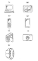
- FIG. 25 is a diagram showing an example of a device having an organic EL display.
- Examples of the organic EL display using the organic semiconductor element manufactured by the organic semiconductor element manufacturing method of the present disclosure include a notebook personal computer (see FIG. 25A) and a tablet terminal (see FIG. 25B).
- Mobile phones see FIG. 25C
- smartphones see FIG. 25D
- video cameras see FIG. 25E
- digital cameras see FIG. 25F
- smart watches see FIG. 25.
- Examples thereof include organic EL displays used in g).
- the detail of the measuring method of Sa and Sz of the surface of a metal plate is as follows.
- test piece was prepared as follows. A square test piece having a side of 5 cm was cut out at the center in the width direction of the metal plate. Then, the position of the surface in the measurement area
- the setting of the laser microscope when the position of the surface of the test piece was measured was as follows.
- RPD is an abbreviation for Real Peak Detection. “With RPD” means that the method of measuring the position of the surface of the test piece by detecting the peak of the reflected light of the laser beam is adopted.
- Example 1 polyimide varnish (UPIA (registered trademark) -ST / Ube Industries Co., Ltd.) was blade-coated on the surface of the metal plate on the side where Sa and Sz were measured, and then at 400 ° C. for 60 minutes in a nitrogen atmosphere. Firing was performed. As a result, a first vapor deposition mask preparation of Example 1 in which a resin layer having a thickness of 6.0 ⁇ m ⁇ 0.5 ⁇ m was laminated on the surface of the metal plate was obtained.
- UPIA registered trademark
- a dry film was bonded to the surface of the metal plate of the first vapor deposition mask preparation of Example 1 above, and a predetermined portion was exposed and developed to form a mask pattern.
- this mask pattern as an anti-etching mask, an unnecessary metal plate was removed using a ferric chloride corrosive solution, and then the mask pattern was washed away.
- the metal plate was used as a metal mask having a metal mask opening, and a second vapor deposition mask preparation of Example 1 in which the metal mask and a resin layer were laminated was obtained.
- a metal frame made of an invar material is prepared, and is fixed by welding so that the metal mask of the second vapor deposition mask preparation of Example 1 is in contact with the metal frame, and the vapor deposition mask preparation of Example 1 is prepared. Produced.
- the frame-equipped vapor deposition mask preparation of Example 1 was placed on the processing stage of the laser processing apparatus with the resin layer facing away from the metal mask. At this time, the processing stage and the resin layer were brought into close contact with each other by bringing the gap between the processing stage and the resin layer into contact with isopropyl alcohol. After that, the resin layer was irradiated with a YAG laser (wavelength 355 nm) through the metal mask opening to penetrate the resin layer to form a resin mask opening (32 ⁇ m ⁇ 34 ⁇ m), and a 400 ppi pattern was formed. A vapor deposition mask with a frame of Example 1 was obtained by obtaining a resin mask.
- a YAG laser wavelength 355 nm
- Example 2 to 3 and Comparative Example 1 Except that a metal plate having a surface roughness different from that of the metal plate was prepared, framed deposition masks of Examples 2 to 3 and Comparative Example 1 were obtained under the same conditions as in Example 1.
- the second vapor deposition mask preparations of Examples 2 to 3 and Comparative Example 1 obtained in the process of manufacturing the vapor deposition mask with frames of Examples 2 to 3 and Comparative Example 1, When the Sa and Sz on the surface of the exposed resin layer were measured, they were as shown in Table 1 below.
- the organic light emitting material Alq 3 was vacuum deposited on a glass substrate (150 mm ⁇ 150 mm ⁇ 0.7 t) with a thickness of 40 nm.
- the vapor deposition mask and the glass substrate were in close contact with each other without any gap.
- the deposited film was observed using an optical microscope (DMRX HC DC300F manufactured by LEICA) and a scanning white interference microscope (Hitachi High-Technologies Bart Scan Co., Ltd.), and the area ratio of the deposited film was calculated.
- the area ratio of the deposited film means that when the area of the pattern to be deposited is 100%, the film thickness is 95% or more of the target value with respect to the area (thus, 38 nm or more when the film thickness is 40 nm). ) In%. In the pattern of 400 ppi, the area ratio of the deposited film was 70% or more. If it is less than that, it is considered that there is a high possibility that a defect will occur due to the effect of misalignment of vapor deposition.
- Measured area ratio is as shown in Table 1 below.
- the area ratio of the vapor deposition film to be formed is 70% or more, the occurrence of defects due to the influence of the positional deviation of the deposition, etc. It was found that can be suppressed.
- the area ratio of the vapor deposition film to be formed is less than 70%. This is considered to be because the resin mask opening cannot be formed with high accuracy because Sa on the surface of the resin mask exposed from the metal mask opening is 0.8 or more.
Landscapes
- Chemical & Material Sciences (AREA)
- Engineering & Computer Science (AREA)
- Metallurgy (AREA)
- Chemical Kinetics & Catalysis (AREA)
- Materials Engineering (AREA)
- Mechanical Engineering (AREA)
- Organic Chemistry (AREA)
- General Chemical & Material Sciences (AREA)
- Manufacturing & Machinery (AREA)
- Physics & Mathematics (AREA)
- General Physics & Mathematics (AREA)
- Electroluminescent Light Sources (AREA)
- Physical Vapour Deposition (AREA)
Priority Applications (5)
| Application Number | Priority Date | Filing Date | Title |
|---|---|---|---|
| JP2018566612A JP6620899B2 (ja) | 2017-03-31 | 2018-03-30 | 蒸着マスク、フレーム付き蒸着マスク、蒸着マスク準備体、蒸着パターン形成方法および有機半導体素子の製造方法 |
| CN201880015841.6A CN110382731B (zh) | 2017-03-31 | 2018-03-30 | 蒸镀掩模、带框体的蒸镀掩模、蒸镀掩模准备体、蒸镀图案形成方法及有机半导体元件的制造方法 |
| KR1020197022599A KR20190132989A (ko) | 2017-03-31 | 2018-03-30 | 증착 마스크, 프레임 부착 증착 마스크, 증착 마스크 준비체, 증착 패턴 형성 방법 및 유기 반도체 소자의 제조 방법 |
| US16/494,802 US10895008B2 (en) | 2017-03-31 | 2018-03-30 | Vapor deposition mask, frame-equipped vapor deposition mask, vapor deposition mask preparation body, vapor deposition pattern forming method, and method for producing organic semiconductor element |
| US17/121,916 US20210214843A1 (en) | 2017-03-31 | 2020-12-15 | Vapor deposition mask, frame-equipped vapor deposition mask, vapor deposition mask preparation body, vapor deposition pattern forming method, and method for producing organic semiconductor element |
Applications Claiming Priority (4)
| Application Number | Priority Date | Filing Date | Title |
|---|---|---|---|
| JP2017072212 | 2017-03-31 | ||
| JP2017-072211 | 2017-03-31 | ||
| JP2017-072212 | 2017-03-31 | ||
| JP2017072211 | 2017-03-31 |
Related Child Applications (2)
| Application Number | Title | Priority Date | Filing Date |
|---|---|---|---|
| US16/494,802 A-371-Of-International US10895008B2 (en) | 2017-03-31 | 2018-03-30 | Vapor deposition mask, frame-equipped vapor deposition mask, vapor deposition mask preparation body, vapor deposition pattern forming method, and method for producing organic semiconductor element |
| US17/121,916 Continuation US20210214843A1 (en) | 2017-03-31 | 2020-12-15 | Vapor deposition mask, frame-equipped vapor deposition mask, vapor deposition mask preparation body, vapor deposition pattern forming method, and method for producing organic semiconductor element |
Publications (1)
| Publication Number | Publication Date |
|---|---|
| WO2018181969A1 true WO2018181969A1 (ja) | 2018-10-04 |
Family
ID=63676261
Family Applications (1)
| Application Number | Title | Priority Date | Filing Date |
|---|---|---|---|
| PCT/JP2018/013798 WO2018181969A1 (ja) | 2017-03-31 | 2018-03-30 | 蒸着マスク、フレーム付き蒸着マスク、蒸着マスク準備体、蒸着パターン形成方法および有機半導体素子の製造方法 |
Country Status (6)
Cited By (2)
| Publication number | Priority date | Publication date | Assignee | Title |
|---|---|---|---|---|
| WO2024162227A1 (ja) * | 2023-01-30 | 2024-08-08 | 大日本印刷株式会社 | フレーム付きマスク、及び、有機デバイスの製造方法 |
| WO2025150503A1 (ja) * | 2024-01-10 | 2025-07-17 | 大日本印刷株式会社 | マスク装置及び有機デバイスの製造方法 |
Families Citing this family (7)
| Publication number | Priority date | Publication date | Assignee | Title |
|---|---|---|---|---|
| WO2019130389A1 (ja) * | 2017-12-25 | 2019-07-04 | 堺ディスプレイプロダクト株式会社 | 蒸着マスク、蒸着方法及び有機el表示装置の製造方法 |
| JP6838693B2 (ja) * | 2019-01-31 | 2021-03-03 | 大日本印刷株式会社 | 蒸着マスク群、電子デバイスの製造方法及び電子デバイス |
| JP7645630B2 (ja) * | 2020-11-18 | 2025-03-14 | 株式会社ジャパンディスプレイ | 蒸着マスクの製造方法 |
| TWI772066B (zh) * | 2021-06-16 | 2022-07-21 | 達運精密工業股份有限公司 | 金屬遮罩基材的製備方法 |
| KR20230020035A (ko) * | 2021-08-02 | 2023-02-10 | 삼성디스플레이 주식회사 | 증착용 마스크 |
| JP3236293U (ja) * | 2021-12-10 | 2022-02-09 | 日本発條株式会社 | メタルマスク |
| WO2025110102A1 (ja) * | 2023-11-22 | 2025-05-30 | 大日本印刷株式会社 | マスク及びマスクの製造方法 |
Citations (3)
| Publication number | Priority date | Publication date | Assignee | Title |
|---|---|---|---|---|
| JP2014121720A (ja) * | 2012-12-21 | 2014-07-03 | V Technology Co Ltd | 蒸着マスクの製造方法 |
| JP2016053194A (ja) * | 2014-09-03 | 2016-04-14 | 大日本印刷株式会社 | 蒸着マスク、フレーム付き蒸着マスク、蒸着マスク準備体、及び有機半導体素子の製造方法 |
| WO2017013903A1 (ja) * | 2015-07-17 | 2017-01-26 | 凸版印刷株式会社 | メタルマスク基材、メタルマスク、および、メタルマスクの製造方法 |
Family Cites Families (9)
| Publication number | Priority date | Publication date | Assignee | Title |
|---|---|---|---|---|
| JPS5288072A (en) | 1976-01-17 | 1977-07-22 | Citizen Watch Co Ltd | Electronic watch with leghting |
| TW575786B (en) * | 2000-03-14 | 2004-02-11 | Takashi Nishi | Exposure controlling photomask and production method thereof |
| KR101439218B1 (ko) | 2012-01-12 | 2014-09-12 | 다이니폰 인사츠 가부시키가이샤 | 증착 마스크, 증착 마스크 장치의 제조 방법, 및 유기 반도체 소자의 제조 방법 |
| TWI601838B (zh) * | 2012-01-12 | 2017-10-11 | 大日本印刷股份有限公司 | A method of manufacturing a vapor deposition mask, and a method of manufacturing an organic semiconductor element |
| JP5846287B1 (ja) * | 2013-12-27 | 2016-01-20 | 大日本印刷株式会社 | フレーム付き蒸着マスクの製造方法、引張装置、有機半導体素子の製造装置及び有機半導体素子の製造方法 |
| JP2017020068A (ja) * | 2015-07-09 | 2017-01-26 | 大日本印刷株式会社 | 蒸着マスク、蒸着マスク準備体、及び有機半導体素子の製造方法 |
| CN205974646U (zh) * | 2015-07-17 | 2017-02-22 | 凸版印刷株式会社 | 蒸镀用金属掩模 |
| WO2017110123A1 (ja) * | 2015-12-25 | 2017-06-29 | 鴻海精密工業股▲ふん▼有限公司 | 蒸着マスク、蒸着マスクの製造方法および有機半導体素子の製造方法 |
| WO2018138824A1 (ja) * | 2017-01-26 | 2018-08-02 | シャープ株式会社 | 蒸着用マスク、蒸着用マスクの製造方法及び有機el表示装置の製造方法 |
-
2018
- 2018-03-30 TW TW107111402A patent/TWI763818B/zh active
- 2018-03-30 KR KR1020197022599A patent/KR20190132989A/ko not_active Ceased
- 2018-03-30 CN CN201880015841.6A patent/CN110382731B/zh active Active
- 2018-03-30 US US16/494,802 patent/US10895008B2/en active Active
- 2018-03-30 JP JP2018566612A patent/JP6620899B2/ja active Active
- 2018-03-30 WO PCT/JP2018/013798 patent/WO2018181969A1/ja active Application Filing
-
2019
- 2019-11-18 JP JP2019208056A patent/JP2020045571A/ja active Pending
-
2020
- 2020-12-15 US US17/121,916 patent/US20210214843A1/en not_active Abandoned
Patent Citations (3)
| Publication number | Priority date | Publication date | Assignee | Title |
|---|---|---|---|---|
| JP2014121720A (ja) * | 2012-12-21 | 2014-07-03 | V Technology Co Ltd | 蒸着マスクの製造方法 |
| JP2016053194A (ja) * | 2014-09-03 | 2016-04-14 | 大日本印刷株式会社 | 蒸着マスク、フレーム付き蒸着マスク、蒸着マスク準備体、及び有機半導体素子の製造方法 |
| WO2017013903A1 (ja) * | 2015-07-17 | 2017-01-26 | 凸版印刷株式会社 | メタルマスク基材、メタルマスク、および、メタルマスクの製造方法 |
Cited By (2)
| Publication number | Priority date | Publication date | Assignee | Title |
|---|---|---|---|---|
| WO2024162227A1 (ja) * | 2023-01-30 | 2024-08-08 | 大日本印刷株式会社 | フレーム付きマスク、及び、有機デバイスの製造方法 |
| WO2025150503A1 (ja) * | 2024-01-10 | 2025-07-17 | 大日本印刷株式会社 | マスク装置及び有機デバイスの製造方法 |
Also Published As
| Publication number | Publication date |
|---|---|
| CN110382731B (zh) | 2022-06-17 |
| US20210214843A1 (en) | 2021-07-15 |
| JPWO2018181969A1 (ja) | 2019-04-04 |
| US10895008B2 (en) | 2021-01-19 |
| TW201842689A (zh) | 2018-12-01 |
| KR20190132989A (ko) | 2019-11-29 |
| US20200259090A1 (en) | 2020-08-13 |
| TWI763818B (zh) | 2022-05-11 |
| JP6620899B2 (ja) | 2019-12-18 |
| CN110382731A (zh) | 2019-10-25 |
| JP2020045571A (ja) | 2020-03-26 |
Similar Documents
| Publication | Publication Date | Title |
|---|---|---|
| JP6620899B2 (ja) | 蒸着マスク、フレーム付き蒸着マスク、蒸着マスク準備体、蒸着パターン形成方法および有機半導体素子の製造方法 | |
| JP6814420B2 (ja) | 蒸着マスクを製造するための金属板、金属板の検査方法、金属板の製造方法、蒸着マスク、蒸着マスク装置及び蒸着マスクの製造方法 | |
| US11211558B2 (en) | Deposition mask device and method of manufacturing deposition mask device | |
| JP7024837B2 (ja) | 蒸着マスクの製造方法、蒸着マスク準備体、フレーム付き蒸着マスク準備体、蒸着マスク、保護シート付き蒸着マスク、フレーム一体型の保護シート付き蒸着マスク、有機半導体素子の製造方法、及び有機elディスプレイの製造方法 | |
| KR101749435B1 (ko) | 금속판, 금속판의 제조 방법, 및 금속판을 사용해서 증착 마스크를 제조하는 방법 | |
| EP3556899A1 (en) | Vapor deposition mask device and method for manufacturing vapor deposition mask device | |
| KR102700053B1 (ko) | 증착 마스크 장치의 제조 방법 및 증착 마스크 장치의 제조 장치 | |
| KR20210116310A (ko) | 유기 디바이스의 제조 장치의 증착실의 평가 방법, 평가 방법에서 사용되는 표준 마스크 장치 및 표준 기판, 표준 마스크 장치의 제조 방법, 평가 방법으로 평가된 증착실을 구비하는 유기 디바이스의 제조 장치, 평가 방법으로 평가된 증착실에서 형성된 증착층을 구비하는 유기 디바이스, 그리고 유기 디바이스의 제조 장치의 증착실의 메인터넌스 방법 | |
| CN111500980B (zh) | 蒸镀掩模以及蒸镀掩模的制造方法 | |
| JP2018111879A (ja) | 金属板、金属板の製造方法、マスクの製造方法およびマスク装置の製造方法 | |
| US20230272517A1 (en) | Deposition mask and method for manufacturing deposition mask | |
| KR20240144240A (ko) | 마스크 및 마스크의 제조 방법 | |
| JP2020007623A (ja) | 蒸着マスク、蒸着マスクの製造方法および有機el表示装置の製造方法 | |
| JP6315140B2 (ja) | 蒸着マスクの製造方法、及び有機半導体素子の製造方法 | |
| JP2024107752A (ja) | フレーム付きマスク、及び、有機デバイスの製造方法 | |
| WO2024128180A1 (ja) | マスク、積層体及びマスクの製造方法 | |
| CN118647752A (zh) | 掩模和掩模的制造方法 | |
| CN120584211A (zh) | 带框架的掩模及有机器件的制造方法 |
Legal Events
| Date | Code | Title | Description |
|---|---|---|---|
| 121 | Ep: the epo has been informed by wipo that ep was designated in this application |
Ref document number: 18776711 Country of ref document: EP Kind code of ref document: A1 |
|
| ENP | Entry into the national phase |
Ref document number: 2018566612 Country of ref document: JP Kind code of ref document: A |
|
| ENP | Entry into the national phase |
Ref document number: 20197022599 Country of ref document: KR Kind code of ref document: A |
|
| NENP | Non-entry into the national phase |
Ref country code: DE |
|
| 122 | Ep: pct application non-entry in european phase |
Ref document number: 18776711 Country of ref document: EP Kind code of ref document: A1 |