WO2018173402A1 - 構造物及び構造物の製造方法 - Google Patents
構造物及び構造物の製造方法 Download PDFInfo
- Publication number
- WO2018173402A1 WO2018173402A1 PCT/JP2017/046400 JP2017046400W WO2018173402A1 WO 2018173402 A1 WO2018173402 A1 WO 2018173402A1 JP 2017046400 W JP2017046400 W JP 2017046400W WO 2018173402 A1 WO2018173402 A1 WO 2018173402A1
- Authority
- WO
- WIPO (PCT)
- Prior art keywords
- metal wire
- fine
- film substrate
- metal
- film
- Prior art date
Links
Images


Classifications
-
- H—ELECTRICITY
- H01—ELECTRIC ELEMENTS
- H01Q—ANTENNAS, i.e. RADIO AERIALS
- H01Q1/00—Details of, or arrangements associated with, antennas
- H01Q1/36—Structural form of radiating elements, e.g. cone, spiral, umbrella; Particular materials used therewith
- H01Q1/38—Structural form of radiating elements, e.g. cone, spiral, umbrella; Particular materials used therewith formed by a conductive layer on an insulating support
-
- B—PERFORMING OPERATIONS; TRANSPORTING
- B32—LAYERED PRODUCTS
- B32B—LAYERED PRODUCTS, i.e. PRODUCTS BUILT-UP OF STRATA OF FLAT OR NON-FLAT, e.g. CELLULAR OR HONEYCOMB, FORM
- B32B15/00—Layered products comprising a layer of metal
- B32B15/04—Layered products comprising a layer of metal comprising metal as the main or only constituent of a layer, which is next to another layer of the same or of a different material
- B32B15/08—Layered products comprising a layer of metal comprising metal as the main or only constituent of a layer, which is next to another layer of the same or of a different material of synthetic resin
-
- G—PHYSICS
- G06—COMPUTING; CALCULATING OR COUNTING
- G06F—ELECTRIC DIGITAL DATA PROCESSING
- G06F3/00—Input arrangements for transferring data to be processed into a form capable of being handled by the computer; Output arrangements for transferring data from processing unit to output unit, e.g. interface arrangements
- G06F3/01—Input arrangements or combined input and output arrangements for interaction between user and computer
- G06F3/03—Arrangements for converting the position or the displacement of a member into a coded form
- G06F3/041—Digitisers, e.g. for touch screens or touch pads, characterised by the transducing means
- G06F3/044—Digitisers, e.g. for touch screens or touch pads, characterised by the transducing means by capacitive means
-
- H—ELECTRICITY
- H01—ELECTRIC ELEMENTS
- H01Q—ANTENNAS, i.e. RADIO AERIALS
- H01Q1/00—Details of, or arrangements associated with, antennas
- H01Q1/12—Supports; Mounting means
- H01Q1/22—Supports; Mounting means by structural association with other equipment or articles
- H01Q1/24—Supports; Mounting means by structural association with other equipment or articles with receiving set
- H01Q1/241—Supports; Mounting means by structural association with other equipment or articles with receiving set used in mobile communications, e.g. GSM
- H01Q1/242—Supports; Mounting means by structural association with other equipment or articles with receiving set used in mobile communications, e.g. GSM specially adapted for hand-held use
- H01Q1/243—Supports; Mounting means by structural association with other equipment or articles with receiving set used in mobile communications, e.g. GSM specially adapted for hand-held use with built-in antennas
Definitions
- the present invention relates to a structure and a method for manufacturing the structure, and more specifically, provided on both surfaces of the film substrate when the film substrate is deformed to form a non-planar surface along a non-planar portion of the structure.
- the present invention relates to a structure capable of preventing disconnection of a formed metal fine line pattern portion and reducing visual discomfort and a method for manufacturing the structure.
- Patent Document 1 discloses a casing component of an electronic device having an antenna function and a capacitive touch panel function. Specifically, a mesh sheet provided with a metal mesh on one side is attached to a member having a curved surface portion corresponding to the outer shape of the casing to form a casing component.
- the metal mesh is provided only on one side of the mesh sheet. Therefore, the mesh sheet has only one function selected from the function of the antenna and the function of the capacitive touch panel.
- Patent Document 1 describes a problem that a thin wire constituting a metal mesh is disconnected when the mesh sheet is deformed so as to follow the outer shape of the housing. In order to solve this problem, it is disclosed that a specific mesh pattern is imparted to a metal mesh. However, this disconnection prevention technique is intended only for fine lines provided on one side of the mesh sheet. Patent Document 1 does not disclose the prevention of disconnection of fine wires provided on both surfaces of a film substrate.
- an object of the present invention is to prevent disconnection of the fine metal wire pattern portions provided on both surfaces of the film base material when the film base material is deformed so as to be non-planar along the non-planar portion of the structure. And it is providing the structure and the manufacturing method of a structure which can reduce a visually uncomfortable feeling.
- the thickness F of the film substrate is 20 ⁇ m or more and 200 ⁇ m or less
- the thickness M of the fine metal wires on at least one surface of the film base is 0.5 ⁇ m or more and 3 ⁇ m or less, 2.
- the fine metal wire has a laminated structure of two or more layers, and has a base layer mainly composed of a metal selected from silver and copper, and a surface layer mainly composed of a metal selected from nickel, aluminum, zinc and tin
- the structure according to any one of 1 to 5. 7).
- the fine metal wire constituting at least a part of the fine metal wire pattern portion includes a non-linear shape,
- the present invention when the film substrate is deformed so as to be non-planar along the non-planar portion of the structure, disconnection of the metal fine line pattern portions provided on both surfaces of the film substrate can be prevented, In addition, it is possible to provide a structure and a method for manufacturing the structure that can reduce visual discomfort.
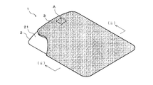
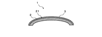
- FIG. 1 is a schematic perspective view of a structure according to an embodiment. Sectional view taken along line (ii)-(ii) in FIG.
- the figure which illustrates notionally the film base material which comprises the structure which concerns on one Embodiment
- the figure explaining an example of a metal fine wire
- the figure explaining an example of thermoforming The figure which illustrates the film base material which comprises the structure which concerns on other embodiment notionally.
- FIG. 1 is a schematic perspective view of a structure according to an embodiment, and shows a state in which a part of a film substrate covering the structure is cut out.
- 2 is a cross-sectional view taken along line (ii)-(ii) in FIG.
- Structure 1 is composed of a structure 2 and a film substrate 3.
- the structure 2 has a non-planar portion 21.
- the “non-planar portion” is a portion that constitutes the surface of the structure 2 and may be a portion that is not included in one plane, and can be constituted by a curved surface or a combination of a plurality of planes. In this embodiment, the case where the non-planar part 21 is comprised by the curved surface is shown.
- the film substrate 3 is provided so as to cover the non-planar portion 21 of the structure 2.
- Thin metal wire pattern portions (not shown in FIGS. 1 and 2) are formed on both surfaces of the film substrate 3. This will be described in detail with reference to FIG.
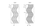
- FIG. 3 is a diagram conceptually illustrating the film base 3 constituting the structure 1 according to the embodiment.
- the film substrate 3 is shown in a state before deformation (planar state).
- the film substrate 3 is deformed so as to be non-planar along the non-planar portion 21 of the structure 2.
- FIG. 3 corresponds to an enlarged view of the film base 3 constituting the region A (corresponding to the non-planar portion 21 of the structure 2) surrounded by a broken line in FIG.
- metal thin line pattern portions 4 and 4 are respectively formed on the front surface 31 and the back surface 32 of the film substrate 3 (in the following description, both the front surface 31 and the back surface 32 are combined with both surfaces 31, 32.)
- the fine metal wire pattern portion 4 is composed of a plurality of fine metal wires 41 arranged two-dimensionally on the film substrate 3.
- the fine metal wires 41 constituting the fine metal wire pattern portion 4 on the surface 31 of the film substrate 3 are provided along the vertical direction as shown by the solid line in FIG. ing.
- the thin metal wires 41 constituting the fine metal wire pattern portion 4 on the back surface 32 of the film substrate 3 are provided along the horizontal direction as shown by the broken lines in FIG. ing.
- Each thin metal wire 41 provided on both surfaces 31 and 32 of the film substrate 3 includes a non-linear shape.
- the fine metal wire 41 includes a wavy element as a non-linear shape.
- the thin metal wire 41 includes a non-linear shape
- the film base 3 is provided on both surfaces of the film base 3 even if the film base 3 is deformed to be non-planar along the non-planar portion 21 of the structure 2.
- the effect of preventing disconnection of the fine metal wire 41 constituting the fine metal wire pattern portion 4 can be obtained.
- the thin metal wire 41 including a non-linear shape functions like a spring and expands and contracts, thereby exhibiting followability to the deformation of the film substrate 3.
- the elasticity of the spring by the thin metal wire 41 including the non-linear shape is exhibited in all directions including the longitudinal direction and the width direction of the thin metal wire 41. Further, this stretchability is exhibited in both the stretching direction and the shrinking direction. Therefore, the effect of preventing disconnection can be obtained regardless of the bending direction of the non-planar portion 21 of the structure 2. Therefore, it is not always necessary to consider the bending direction of the non-planar portion 21 of the structure 2 when patterning the thin metal wire 41. For example, it is also preferable to form the fine metal wires 41 in the same pattern for each of the non-planar portion 21 of the structure 2 and the planar portion of the structure 2.
- the bent state is different between the front surface 31 and the back surface 32 of the film base 3.
- the front surface 31 extends and the back surface 32 contracts.
- the surface 31 shrinks and the back surface 32 extends.
- the metal fine wires 41 on both surfaces 31 and 32 of the film base 3 have elasticity like a spring, so that both the expansion and contraction that occur simultaneously on both surfaces 31 and 32 of the film base 3 are prevented. The effect of preventing disconnection is exhibited. Therefore, even when the structure 2 has the convex non-planar portion 21, the concave non-planar portion 21, or both, the fine metal wires 31 and 32 on both surfaces 31 and 32 of the film substrate 3. The disconnection of 41 can be prevented.
- the shape of the metal thin wire 41 as a whole may be curved, for example, to draw an arc, or may be linear as shown in FIG.
- the term “linear” means that the centers of the amplitudes associated with the meandering of the fine metal wires 41 are arranged on a straight line.
- the shape of the metal thin wire 41 as a whole here describes the state before the deformation of the film base 3, but the state before the deformation from the stretched state of the film base 3 even after the deformation. I can confirm.
- each thin metal wire 41 provided on both surfaces 31 and 32 of the film base 3 includes a non-linear shape, an effect of reducing visual discomfort can be obtained. This will be described below.
- the conventional metal mesh interferes with the pixel array included in the image display element. Can cause moiré and give a visual discomfort.
- the metal thin wire 41 includes a non-linear shape, such interference is prevented, moire is less likely to occur, and visual discomfort is reduced. Such an effect is exhibited not only when the pixel array is provided but also when an element having a periodic pattern is provided, for example.
- the film base 3 is transparent, if a metal mesh that does not include a non-linear shape is provided on both sides 31 and 32 of the film base 3, interference occurs between the metal meshes on both sides 31 and 32 and moire occurs. , Can give a visual discomfort. On the other hand, when the metal thin wire 41 includes a non-linear shape, such interference is prevented, moire is less likely to occur, and visual discomfort is reduced.
- the film substrate 3 is not transparent and cannot be seen through, an effect of reducing visual discomfort can be obtained.
- the conventional metal mesh interferes with the periodic pattern and causes moire. Can occur.
- the metal thin wire 41 includes a non-linear shape, such interference is prevented, moire is less likely to occur, and visual discomfort is reduced.
- an effect that hardly causes a visual discomfort is produced. can get.
- the film substrate 3 on which the metal fine line pattern portions 4 and 4 are formed on both surfaces 31 and 32 can be used as, for example, a capacitive sensor or the like.
- the X-direction position detection electrode and the Y-direction one detection electrode can be configured by the metal fine line pattern portions 4 and 4 on both surfaces 31 and 32, compared with the case where the metal fine line pattern portion is formed only on one side. Accurate position detection can be performed. Further, as described in “3. Applications”, the film base 3 in which the fine metal wire pattern portions 4 and 4 are formed on the both surfaces 31 and 32 also has an effect that it can be multi-functionalized by giving different functions to each side. .
- the film substrate 3 preferably has a single layer structure (one sheet). Thereby, for example, compared with the case where the film substrate 3 has a laminated structure (for example, a case where two films are laminated), a positional deviation between the films occurs when the film is integrally formed with the structure 2. No effect is obtained. Thereby, the function (position detection function in the example of a touch sensor) by the metal thin wire
- the combined fine metal wire density of the fine metal wire pattern portions 4 and 4 formed on both surfaces 31 and 32 of the film base material 3 is preferably less than 20%.
- the fine metal wire density (%) is the percentage of the area covered with the fine metal wires 41 in the surface area of the film substrate 3 constituting the fine metal wire pattern portion 4.
- the total fine metal wire density (%) is a value obtained by adding the fine metal wire densities (%) obtained for each of the front surface 31 and the back surface 32 of the film substrate 3.
- FIG. 4 is a cross-sectional view of the film base material 3 on which the fine metal wires 41 are formed, and shows a state in which the fine metal wires 41 are cut along a cross section orthogonal to the longitudinal direction.
- the fine metal wire 41 has a two-layer laminated structure.
- the thin metal wire 41 preferably has, as a laminated structure, a base layer 411 mainly composed of a metal selected from silver and copper, and an outer layer 412 mainly composed of a metal selected from nickel, aluminum, zinc and tin. Excellent conductivity is exhibited by the metal constituting the base layer 411. Further, the metal constituting the outer layer 412 can further improve the conductivity. Furthermore, the hiding effect is exhibited by providing the outer layer 412. The concealing effect is an effect that makes it difficult to visually recognize the thin metal wire 41.
- the image displayed by the structure 2, the color of the structure 2, and the like can be viewed through the film substrate 3.
- the metal fine line 41 becomes difficult to visually recognize due to the concealing effect, so that the image can be clearly recognized.
- the fine metal wire may have a laminated structure of three or more layers.
- the thin metal wire has a laminated structure of three or more layers, it can have one or more intermediate layers (not shown) between the base layer 411 and the outer layer 412 described above.
- the metal thin wire may have a single layer structure.
- middle layer or a single layer structure can be selected from the metal illustrated about the base layer 411 and the outer layer 412, for example.
- the thickness F of the film substrate 3 is preferably 20 ⁇ m or more and 200 ⁇ m or less, and the thickness M of the fine metal wire 41 is preferably 0.5 ⁇ m or more and 3 ⁇ m or less. Furthermore, the M / F ratio is preferably 0.004 to 0.05, particularly when the thicknesses F and M are in the above ranges. Thereby, the electroconductivity of the metal fine wire 41 is ensured favorably, and the workability at the time of integral molding is also improved. Moreover, the effect by which the conduction
- the above-described condition relating to the thickness M of the fine metal wire 41 only needs to be satisfied for the fine metal wire 41 on at least one of the both surfaces 31 and 32 of the film base 3. More preferably, this condition is satisfied for the thin metal wires 41 on both surfaces 31 and 32 of the film substrate 3.
- the material of the structure 2 is not particularly limited, but is preferably a resin or the like.
- the resin include polyethylene terephthalate (PET) resin, polyethylene naphthalate (PEN) resin, polybutylene terephthalate resin, cellulose resin (polyacetyl cellulose, cellulose diacetate, cellulose triacetate, etc.), polyethylene resin, polypropylene resin, Methacrylic resin, cyclic polyolefin resin, polystyrene resin, acrylonitrile- (poly) styrene copolymer (AS resin), acrylonitrile-butadiene-styrene copolymer (ABS resin), polyvinyl chloride resin, poly (meth)
- a thermoplastic resin is preferably used when the resin is melted during the molding of the structure 2 as in the insert molding described later.
- the shape of the structure 2 only needs to have the above-described non-planar portion at any part of the surface of the structure 2.
- the film substrate 3 examples include a transparent substrate.
- the degree of transparency of the transparent substrate is not particularly limited, and the light transmittance may be anywhere from several% to several tens%, and the spectral transmittance may be any value. These light transmittance and spectral transmittance can be appropriately determined according to the application and purpose.
- the material for the film substrate is not particularly limited, and is preferably a resin, for example.
- resin what was illustrated as a material of the structure 2, for example can be used, and if these materials are used, favorable transparency can be provided to a base material.
- the material of the thin metal wire 41 is not particularly limited as long as it is a metal, and examples thereof include silver, copper, nickel, aluminum, zinc, and tin.
- a metal fine wire can be comprised by 1 type, or 2 or more types selected from these metals. When two or more kinds of metals are used in combination, two or more kinds of metals may be mixed and used, but as described above, it is preferable to form a laminated structure composed of a plurality of metal layers made of different metals.
- the metal fine wire 41 may be configured as an aggregate of metal fine particles.
- the followability of the thin metal wire 41 with respect to the deformation of the film substrate 3 is further improved, and disconnection is further prevented.
- the metal thin wire 41 is appropriately thinned (in a sparse state) to improve stretchability.
- each metal fine particle which comprises an aggregate does not necessarily need to be a completely independent particle
- the thin metal wire 41 has a laminated structure, it is preferable that at least one layer, preferably at least one layer including the base layer 411, is constituted by an aggregate of metal fine particles.
- a printing method using an ink containing fine metal particles can be used. This method will be described in more detail in “2. Manufacturing method of structure” below.
- the structure is constituted by the structure 2 and the film substrate 3 provided with the metal fine line pattern portions 4 on both sides, as described in the above “1. structure”.
- the fine metal wire pattern portion 4 When forming the fine metal wire pattern portion 4 on the film base 3, a printing method, photolithography, or the like is used, and the printing method is particularly preferably used.
- the printing method for example, an ink containing metal fine particles can be applied on the substrate to form the metal fine wire 41 constituting the metal fine wire pattern portion 4.
- the printing method is not particularly limited, and examples thereof include a screen printing method, a relief printing method, an intaglio printing method, an offset printing method, a flexographic printing method, an inkjet method, and the like. Among these, an inkjet method is preferable.
- the droplet discharge method of the inkjet head in the inkjet method is not particularly limited, and examples thereof include a piezo method and a thermal method.
- a line-like liquid 5 made of ink containing metal fine particles is applied on the surface 31 of the substrate 3.
- a non-linear line-shaped liquid 5 including a wavy line element is formed.
- a pair of fine metal wires 41 and 41 are formed by selectively depositing metal fine particles on both edges along the longitudinal direction of the line-shaped liquid 5.
- the pair of fine metal wires 41 and 41 can be formed in parallel to each other.
- the line width of the thin metal wire 41 is narrower than the line width of the line-like liquid 5 and can be set to, for example, 20 ⁇ m or less, 15 ⁇ m or less, and further 10 ⁇ m or less.
- wire width of the metal fine wire 41 is not specifically limited, From viewpoints, such as providing stable electroconductivity, it can be 1 micrometer or more, for example. From the viewpoint of making it difficult to visually recognize the fine metal wire 41, the line width of the fine metal wire 41 is preferably less than 10 ⁇ m.
- the fine metal wire 41 as an aggregate of fine metal particles can be formed thin and stably. Thereby, the followability of the fine metal wire 41 with respect to the deformation of the film base 3 is further improved, and the disconnection is prevented more favorably.
- Examples of the metal constituting the metal fine particles to be included in the ink include Au, Pt, Ag, Cu, Ni, Cr, Rh, Pd, Zn, Co, Mo, Ru, W, Os, Ir, Fe, Mn, and Ge. , Sn, Ga, In and the like. Among these, Au, Ag, and Cu are preferable, and Ag is particularly preferable.
- the average particle diameter of the metal fine particles can be, for example, 1 to 100 nm, further 3 to 50 nm.
- the average particle diameter is a volume average particle diameter, and can be measured by “Zeta Sizer 1000HS” manufactured by Malvern.
- the solvent used in the ink is not particularly limited, and may include one or more selected from water and organic solvents.
- the organic solvent include 1,2-hexanediol, 2-methyl-2,4-pentanediol, 1,3-butanediol, 1,4-butanediol, alcohols such as propylene glycol, diethylene glycol monomethyl ether,
- ethers such as diethylene glycol monoethyl ether, diethylene glycol monobutyl ether, triethylene glycol monomethyl ether, dipropylene glycol monomethyl ether, and dipropylene glycol monoethyl ether.
- the ink can contain other components such as a surfactant.
- the surfactant is not particularly limited, and examples thereof include a silicon surfactant.
- the concentration of the surfactant in the ink can be, for example, 1% by weight or less.
- the drying method of the ink (line liquid) applied on the film substrate may be natural drying or forced drying.
- the drying method used for forced drying is not particularly limited. For example, a method of heating the surface of the substrate to a predetermined temperature, a method of forming an air flow on the surface of the substrate, or the like can be used alone or in combination. .
- the airflow can be formed by blowing or sucking using a fan or the like, for example.
- Post-treatment can be applied to the fine metal wire formed on the substrate.
- a baking process, a plating process, etc. are mentioned, for example. After performing the baking treatment, a plating treatment may be performed.
- Examples of the baking treatment include light irradiation treatment and heat treatment.
- light irradiation treatment for example, gamma rays, X-rays, ultraviolet rays, visible light, infrared rays (IR), microwaves, radio waves, and the like can be used.
- heat treatment for example, hot air, a heating stage, a heating press, or the like can be used.
- plating treatment examples include electroless plating and electrolytic plating.
- the fine metal wires can be selectively plated using the conductivity of the fine metal wires.
- a fine metal wire having the laminated structure shown in FIG. 4 can be formed.
- a plurality of times of plating processes using different plating metals may be performed.
- a plurality of metal layers can be laminated on the conductive thin wire by a plurality of plating processes.
- the outer layer 412 can be laminated on the base layer 411 shown in FIG. 4 after laminating one or more metal layers as an intermediate layer.
- the fine metal wire pattern portion 4 constituted by the fine metal wires 41 can be formed.
- a film substrate 3 having metal pattern portions (not shown in FIG. 6) on both sides is supplied to molds 6a and 6b for forming a structure.
- molten resin 20 for forming the structure 2 is injected into the molds 6a and 6b.
- the resin 20 is injected so as to come into contact with the back surface 32 side of the film base 3.
- the injected resin 20 is solidified by cooling to form the structure 2.
- the resin 20 is fused to the back surface 32 of the film base 3, and the structure 2 and the film base 3 are integrated.
- the film substrate 3 is deformed so as to form a non-planar surface along the non-planar portion 21 of the structure 2.
- the film base material 3 is deformed (preformed) in advance before the molten resin is injected into the molds 6a and 6b.
- the method of deforming the film base 3 include a method of performing molding such as pressure molding or vacuum / pressure forming while the film base 3 is heated and softened.
- the film base 3 may be deformed by heat from the molten resin and an injection pressure.
- the metal fine wires of the metal fine wire pattern portions on both surfaces of the film base material 3 include a non-linear shape, thereby obtaining an effect of preventing disconnection of the metal fine wires accompanying the deformation of the film base material 3.
- the film substrate 3 may be supplied to the mold in a state where another layer (not shown) is laminated on the front surface 31 side or the back surface 32 side of the film base material 3. .
- the structure 1 in which another layer is laminated between the film base 3 and the structure 2 or the structure 1 in which another layer is laminated on the surface of the film base 3 is provided. can get.
- the thin metal wire includes a non-linear shape, thereby preventing the occurrence of moire and reducing the visual discomfort. .
- the non-linear shape given to the fine metal wire includes a wavy element is mainly shown, but the present invention is not limited to this.
- the non-linear shape should just contain the inclined line element which inclines with respect to the direction which connects the end from the one end of a metal fine wire at the shortest.
- the inclined line element can be constituted by a straight line or a curved line. Further, by combining a plurality of inclined line elements, the above-described wavy line element or zigzag element can be applied to the fine metal wire 41.
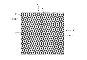
- FIG. 7 shows a state in which a zigzag element is added to the metal thin wire 41 as a non-linear shape.
- the case where the coffee stain phenomenon is used will be described as an example.
- the line-like liquid 5 shown in FIG. 5 may be formed in a zigzag shape.
- the non-linear shape provided to the fine metal wire 41 includes an element that repeatedly meanders to the left and right with respect to the longitudinal direction of the fine metal wire 41, such as a wavy line element or a zigzag element.
- the present invention is not limited to this.
- the effect of the present invention is exhibited as long as the fine metal wire constituting at least a part of the fine metal wire pattern portion includes a non-linear shape.
- Application The application of the structure 1 is not particularly limited, and can be used for various devices.
- the fine metal wire 41 constituting the fine metal wire pattern portion 4 of the structure 1 can be used as a conductive member such as an electric wiring or an electrode according to the type of the device.
- a conductive member such as an electric wiring or an electrode according to the type of the device.
- one electrode may be constituted by a plurality of fine metal wires 41 arranged in parallel.
- the fine metal wire pattern portions 4 and 4 formed on both surfaces of the film substrate 3 may be configured to exhibit one function on both surfaces, but perform different functions on each surface (one surface at a time). Preferably, it is configured.
- a touch switch function for constituting a capacitance sensor can be given to the fine metal line pattern portion 4 on the back surface 32.
- a heating element function can be imparted to the thin metal wire pattern portion 4 on the surface 31 by constituting a heating element (heater).
- a heating element for heat generation, Joule heat generated by energization of the thin metal wire 41 can be used.
- an antenna function for transmitting and receiving electromagnetic waves for communication or the like may be imparted to the thin metal wire pattern portion 4 on the surface 31.
- the function of the fine metal wire pattern portion 4 may be interchanged between the front surface 31 and the back surface 32. Moreover, the function demonstrated as what is provided to the metal fine wire pattern part 4 of each surface may be provided as a function exhibited by the metal fine wire pattern parts 4 and 4 of both surfaces.
- Example 1 The structure 2 having a non-planar portion and the film base 3 covering the non-planar portion 21 of the structure 2 are integrated by thermoforming by insert molding similar to that shown in FIG. A structure 1 similar to that shown was produced.
- the fine metal wire pattern portions 4 and 4 are formed in advance on both surfaces of the film substrate 3 used for insert molding. Similarly to the one shown in FIG. 3, the fine metal wire 41 constituting the fine metal wire pattern portion 4 includes a wavy element as a non-linear shape.
- the fine metal wire 41 was formed by a printing method using a coffee stain phenomenon (see FIG. 5).
- Example 1 (Comparative Example 1) In Example 1, a structure was manufactured in the same manner as in Example 1 except that the fine metal wires were linear.
- Example 1 and Comparative Example 1 Evaluation method of disconnection rate About the structure obtained in Example 1 and Comparative Example 1, the thin metal wires 41 on both surfaces of the film substrate were observed with a microscope, and the disconnection rate (%) was calculated. The results are shown in Table 1.
- Example 1 ⁇ Evaluation of Example 1 and Comparative Example 1> From Table 1, it can be seen that in Example 1 in which a non-linear shape is imparted to the metal thin wire, disconnection of the metal thin wire can be prevented in comparison with Comparative Example 1 in which a linear shape is imparted to the metal thin wire. Moreover, in Example 1, it turns out that the effect which can reduce a visual discomfort is acquired. Furthermore, as a reference example, when a transparent film on which a lattice pattern was printed was superimposed on a transparent film on which no fine metal wires were formed, all 20 subjects answered that there was no sense of incongruity.
- the film base material of the present invention in which the thin metal wire provided with the non-linear shape is formed is visually uncomfortable to the extent that there is no significant discoloration compared with the transparent film on which the thin metal wire is not formed. It can be seen that it can be reduced.
- Example 2 In Example 1, the thickness F of the film substrate and the thickness M of the fine metal wires were changed as shown in Table 2, The structures according to 2-1 to 2-7 were manufactured. Here, the thickness M of the fine metal wire was the same value on the front surface and the back surface of the film substrate. About the obtained structure, the failure rate (%) was measured. Here, continuity failure was observed as the failure content. The results are shown in Table 2 together with the M / F ratio.
- Example 2 ⁇ Evaluation of Example 2> From Table 2, test No. 1 satisfying the conditions that the thickness F of the film substrate is 20 ⁇ m or more and 200 ⁇ m or less, the thickness M of the fine metal wire is 0.5 ⁇ m or more and 3 ⁇ m or less, and the M / F ratio is 0.004 to 0.05. Test Nos. 2-1 to 2-4 do not satisfy this condition. It can be seen that the failure rate can be further reduced in comparison with 2-5 to 2-7.
- Structure 2 Structure 21: Non-planar portion 3: Film substrate 31: Front surface 32: Back surface 4: Metal fine wire pattern portion 41: Metal fine wire
Abstract
Description
非平面部分を有する構造体と、前記構造体の前記非平面部分を被覆するフィルム基材とを一体成形してなる構造物であって、
前記非平面部分の少なくとも一部を被覆する前記フィルム基材の両面に金属細線パターン部が形成されており、
前記金属細線パターン部の少なくとも一部を構成する金属細線が非直線形状を含む構造物。
2.
前記フィルム基材の厚みFが20μm以上200μm以下であり、
前記フィルム基材の少なくとも一方の面の前記金属細線の厚みMが0.5μm以上3μm以下であり、
M/F比が0.004~0.05である前記1記載の構造物。
3.
前記フィルム基材の両面に形成された前記金属細線パターン部の合算の金属細線密度が20%未満である前記1又は2記載の構造物。
4.
前記フィルム基材の片面の前記金属細線パターン部、又は両面の前記金属細線パターン部に、タッチスイッチ機能が付与されている前記1~3の何れかに記載の構造物。
5.
前記フィルム基材の片面の前記金属細線パターン部、又は両面の前記金属細線パターン部に、発熱体機能又はアンテナ機能が付与されている前記1~4の何れかに記載の構造物。
6.
前記金属細線は2層以上の積層構造を有し、銀及び銅から選ばれる金属を主成分とする基層と、ニッケル、アルミニウム、亜鉛及びスズから選ばれる金属を主成分とする表層とを有する前記1~5の何れかに記載の構造物。
7.
非平面部分を有する構造体と、前記構造体の前記非平面部分を被覆するフィルム基材とを一体化して構造物を製造する構造物の製造方法であって、
前記非平面部分の少なくとも一部を被覆する前記フィルム基材の両面に金属細線パターン部が形成されており、
前記金属細線パターン部の少なくとも一部を構成する金属細線が非直線形状を含み、
前記構造体とフィルム基材とを加熱成形により一体化する構造物の製造方法。
図1は一実施形態に係る構造物の概略斜視図であり、構造体を被覆するフィルム基材の一部を切り欠いた様子を示している。図2は図1における(ii)-(ii)線断面図である。
次に、構造物の製造方法について説明する。上記「1.構造物」についてした説明は「2.構造物の製造方法」に適宜援用される。また、「構造物の製造方法」についてする説明は上記「1.構造物」に適宜援用される。
構造物1の用途は格別限定されず、種々のデバイスに用いることができる。
図6に示したものと同様のインサート成形によって、非平面部分を有する構造体2と、構造体2の非平面部分21を被覆するフィルム基材3とを加熱成形により一体化して、図1に示したものと同様の構造物1を製造した。
実施例1において、金属細線を直線形状にしたこと以外は、実施例1と同様にして、構造物を製造した。
(1)断線率の評価方法
実施例1及び比較例1において得られた構造物について、フィルム基材の両面の金属細線41を顕微鏡で観察し、断線率(%)を算出した。結果を表1に示す。
実施例1及び比較例1において得られた構造物のフィルム基材上に、格子パターンが印刷された透明フィルムを重ね、モアレの発生に伴う視覚的な違和感の有無について試験した。具体的には、20人の被験者に、構造物のフィルム基材上に重ねられた透明フィルムを目視してもらい、視覚的な違和感ありと回答した被験者数及び視覚的な違和感なしと回答した被験者数をそれぞれ集計した。結果を表1に示す。

表1より、金属細線に非直線形状を付与した実施例1では、金属細線に直線形状を付与した比較例1との対比で、金属細線の断線を防止できることがわかる。また、実施例1では、視覚的な違和感を低減できる効果が得られることがわかる。更に、参考例として、金属細線が形成されていない透明フィルムに、格子パターンが印刷された透明フィルムを重ねた場合は、20人の被験者全員が違和感なしと回答した。このことから、非直線形状が付与された金属細線が形成された本発明のフィルム基材は、金属細線が形成されていない透明フィルムと比較して大きな遜色がない程度に、視覚的な違和感を低減できることがわかる。
実施例1において、フィルム基材の厚みF、金属細線の厚みMを、表2に示すように変化させて、試験No.2-1~2-7に係る構造物を製造した。ここで、金属細線の厚みMは、フィルム基材の表面と裏面とで同じ値とした。得られた構造物について、故障率(%)を測定した。ここでは、故障内容として、導通故障を観察した。M/F比と併せて、結果を表2に示す。

表2より、フィルム基材の厚みFが20μm以上200μm以下、金属細線の厚みMが0.5μm以上3μm以下、且つM/F比が0.004~0.05という条件を満たす試験No.2-1~2-4は、この条件を満たさない試験No.2-5~2-7との対比で、故障率を更に低下できることがわかる。
2:構造体
21:非平面部分
3:フィルム基材
31:表面
32:裏面
4:金属細線パターン部
41:金属細線
Claims (7)
- 非平面部分を有する構造体と、前記構造体の前記非平面部分を被覆するフィルム基材とを一体成形してなる構造物であって、
前記非平面部分の少なくとも一部を被覆する前記フィルム基材の両面に金属細線パターン部が形成されており、
前記金属細線パターン部の少なくとも一部を構成する金属細線が非直線形状を含む構造物。 - 前記フィルム基材の厚みFが20μm以上200μm以下であり、
前記フィルム基材の少なくとも一方の面の前記金属細線の厚みMが0.5μm以上3μm以下であり、
M/F比が0.004~0.05である請求項1記載の構造物。 - 前記フィルム基材の両面に形成された前記金属細線パターン部の合算の金属細線密度が20%未満である請求項1又は2記載の構造物。
- 前記フィルム基材の片面の前記金属細線パターン部、又は両面の前記金属細線パターン部に、タッチスイッチ機能が付与されている請求項1~3の何れかに記載の構造物。
- 前記フィルム基材の片面の前記金属細線パターン部、又は両面の前記金属細線パターン部に、発熱体機能又はアンテナ機能が付与されている請求項1~4の何れかに記載の構造物。
- 前記金属細線は2層以上の積層構造を有し、銀及び銅から選ばれる金属を主成分とする基層と、ニッケル、アルミニウム、亜鉛及びスズから選ばれる金属を主成分とする表層とを有する請求項1~5の何れかに記載の構造物。
- 非平面部分を有する構造体と、前記構造体の前記非平面部分を被覆するフィルム基材とを一体化して構造物を製造する構造物の製造方法であって、
前記非平面部分の少なくとも一部を被覆する前記フィルム基材の両面に金属細線パターン部が形成されており、
前記金属細線パターン部の少なくとも一部を構成する金属細線が非直線形状を含み、
前記構造体とフィルム基材とを加熱成形により一体化する構造物の製造方法。
Priority Applications (3)
| Application Number | Priority Date | Filing Date | Title |
|---|---|---|---|
| JP2019506945A JPWO2018173402A1 (ja) | 2017-03-23 | 2017-12-25 | 構造物及び構造物の製造方法 |
| CN201780088569.XA CN110431921A (zh) | 2017-03-23 | 2017-12-25 | 构造物以及构造物的制造方法 |
| KR1020197027232A KR102143311B1 (ko) | 2017-03-23 | 2017-12-25 | 구조물 및 구조물의 제조 방법 |
Applications Claiming Priority (2)
| Application Number | Priority Date | Filing Date | Title |
|---|---|---|---|
| JP2017-057321 | 2017-03-23 | ||
| JP2017057321 | 2017-03-23 |
Publications (1)
| Publication Number | Publication Date |
|---|---|
| WO2018173402A1 true WO2018173402A1 (ja) | 2018-09-27 |
Family
ID=63586351
Family Applications (1)
| Application Number | Title | Priority Date | Filing Date |
|---|---|---|---|
| PCT/JP2017/046400 WO2018173402A1 (ja) | 2017-03-23 | 2017-12-25 | 構造物及び構造物の製造方法 |
Country Status (4)
| Country | Link |
|---|---|
| JP (1) | JPWO2018173402A1 (ja) |
| KR (1) | KR102143311B1 (ja) |
| CN (1) | CN110431921A (ja) |
| WO (1) | WO2018173402A1 (ja) |
Cited By (1)
| Publication number | Priority date | Publication date | Assignee | Title |
|---|---|---|---|---|
| CN114023781A (zh) * | 2021-10-08 | 2022-02-08 | 业成科技(成都)有限公司 | 曲面电子装置及其制造方法 |
Citations (5)
| Publication number | Priority date | Publication date | Assignee | Title |
|---|---|---|---|---|
| JP2005167216A (ja) * | 2003-11-12 | 2005-06-23 | Polymatech Co Ltd | 三次元成形回路シート、三次元成形回路部品およびそれらの製造方法 |
| JP2008262981A (ja) * | 2007-04-10 | 2008-10-30 | Tsuchiya Co Ltd | フレキシブルプリント基板、およびその製造方法 |
| JP2012242871A (ja) * | 2011-05-16 | 2012-12-10 | Nissha Printing Co Ltd | 曲面タッチパネル、その製造方法及び曲面タッチパネル付表示装置 |
| WO2013190884A1 (ja) * | 2012-06-19 | 2013-12-27 | 日本写真印刷株式会社 | タッチパネル、タッチパネルの製造方法 |
| WO2015115503A1 (ja) * | 2014-01-28 | 2015-08-06 | コニカミノルタ株式会社 | 導電性パターン、導電性パターン付き基材、導電性パターン付き基材の製造方法、表面に導電性パターンを有する構造体及び該構造体の製造方法 |
Family Cites Families (4)
| Publication number | Priority date | Publication date | Assignee | Title |
|---|---|---|---|---|
| US20100294344A1 (en) * | 2005-09-28 | 2010-11-25 | Sipix Chemical Inc. | Decoration film and decoration device |
| US8003900B2 (en) | 2008-02-19 | 2011-08-23 | Nissha Printing Co., Ltd. | Mesh sheet and housing for electronic devices |
| JP6427860B2 (ja) * | 2013-10-15 | 2018-11-28 | コニカミノルタ株式会社 | プリンデッドエレクトロニクスデバイスおよび電子機能パターンを形成する方法 |
| WO2016181824A1 (ja) * | 2015-05-11 | 2016-11-17 | 富士フイルム株式会社 | 導電性積層体の製造方法、導電性積層体、被めっき層前駆体層付き基板、被めっき層付き基板、タッチセンサー |
-
2017
- 2017-12-25 JP JP2019506945A patent/JPWO2018173402A1/ja active Pending
- 2017-12-25 CN CN201780088569.XA patent/CN110431921A/zh active Pending
- 2017-12-25 WO PCT/JP2017/046400 patent/WO2018173402A1/ja active Application Filing
- 2017-12-25 KR KR1020197027232A patent/KR102143311B1/ko active IP Right Grant
Patent Citations (5)
| Publication number | Priority date | Publication date | Assignee | Title |
|---|---|---|---|---|
| JP2005167216A (ja) * | 2003-11-12 | 2005-06-23 | Polymatech Co Ltd | 三次元成形回路シート、三次元成形回路部品およびそれらの製造方法 |
| JP2008262981A (ja) * | 2007-04-10 | 2008-10-30 | Tsuchiya Co Ltd | フレキシブルプリント基板、およびその製造方法 |
| JP2012242871A (ja) * | 2011-05-16 | 2012-12-10 | Nissha Printing Co Ltd | 曲面タッチパネル、その製造方法及び曲面タッチパネル付表示装置 |
| WO2013190884A1 (ja) * | 2012-06-19 | 2013-12-27 | 日本写真印刷株式会社 | タッチパネル、タッチパネルの製造方法 |
| WO2015115503A1 (ja) * | 2014-01-28 | 2015-08-06 | コニカミノルタ株式会社 | 導電性パターン、導電性パターン付き基材、導電性パターン付き基材の製造方法、表面に導電性パターンを有する構造体及び該構造体の製造方法 |
Cited By (1)
| Publication number | Priority date | Publication date | Assignee | Title |
|---|---|---|---|---|
| CN114023781A (zh) * | 2021-10-08 | 2022-02-08 | 业成科技(成都)有限公司 | 曲面电子装置及其制造方法 |
Also Published As
| Publication number | Publication date |
|---|---|
| KR102143311B1 (ko) | 2020-08-10 |
| JPWO2018173402A1 (ja) | 2020-01-23 |
| CN110431921A (zh) | 2019-11-08 |
| KR20190120273A (ko) | 2019-10-23 |
Similar Documents
| Publication | Publication Date | Title |
|---|---|---|
| US10091917B2 (en) | Transparent EMI shielding/absorbing film | |
| CN104376899B (zh) | 电子装置、触控屏、透明导电膜及透明导电膜的制备方法 | |
| JP6047994B2 (ja) | 透明導電性素子およびその製造方法、入力装置、電子機器、ならびに透明導電層の加工方法 | |
| JP5225178B2 (ja) | 静電容量センサ及びその製造方法 | |
| WO2013111807A1 (ja) | 透明導電性素子およびその製造方法、入力装置、電子機器、ならびに薄膜のパターニング方法 | |
| WO2018173402A1 (ja) | 構造物及び構造物の製造方法 | |
| JP6733586B2 (ja) | 透明導電体及び透明導電体の製造方法 | |
| KR101323601B1 (ko) | 터치 센서 일체형 3차원 디스플레이 및 그 제조방법 | |
| JP2013152578A (ja) | 透明導電性素子、入力装置、電子機器および透明導電性素子作製用原盤 | |
| WO2012144643A1 (ja) | 透明導電性素子、入力装置、電子機器、透明導電性素子の製造方法 | |
| JP5754739B2 (ja) | タッチセンサ | |
| JP2019016491A (ja) | 透明面状発熱体、透明面状発熱体製造方法 | |
| JP2019008361A (ja) | センサーフィルム及びセンサーフィルム付き画像表示装置 | |
| EP2587353A2 (en) | Touch panel | |
| CN104637573B (zh) | 导电薄膜结构 | |
| WO2017056977A1 (ja) | タッチパネルセンサーの製造方法及びタッチパネルセンサー | |
| JP2018158517A (ja) | 積層導電フィルム及び積層導電フィルムの製造方法 | |
| JP2018180741A (ja) | 細線パターン及び細線パターンの形成方法 | |
| CN111133405A (zh) | 触摸面板传感器以及触摸面板传感器的制造方法 | |
| KR20120116280A (ko) | 터치 센서 일체형 3차원 디스플레이 및 그 제조방법 | |
| JP7063464B2 (ja) | 可撓性加飾積層シート、タッチパネル用モジュールおよびタッチパネル | |
| JP6173831B2 (ja) | 透明導電性シート、および透明導電性シートを用いたタッチパネル | |
| JP2019164069A5 (ja) | ||
| WO2019234841A1 (ja) | ケーブル付きフレキシブル回路及びその製造方法、並びにケーブル付きフレキシブル回路中間体 | |
| JP6794325B2 (ja) | 導電性基材、導電性基材の製造方法、積層体およびタッチパネル |
Legal Events
| Date | Code | Title | Description |
|---|---|---|---|
| 121 | Ep: the epo has been informed by wipo that ep was designated in this application |
Ref document number: 17902220 Country of ref document: EP Kind code of ref document: A1 |
|
| ENP | Entry into the national phase |
Ref document number: 2019506945 Country of ref document: JP Kind code of ref document: A |
|
| ENP | Entry into the national phase |
Ref document number: 20197027232 Country of ref document: KR Kind code of ref document: A |
|
| NENP | Non-entry into the national phase |
Ref country code: DE |
|
| 122 | Ep: pct application non-entry in european phase |
Ref document number: 17902220 Country of ref document: EP Kind code of ref document: A1 |