WO2018173095A1 - プラズマ処理装置 - Google Patents
プラズマ処理装置 Download PDFInfo
- Publication number
- WO2018173095A1 WO2018173095A1 PCT/JP2017/011093 JP2017011093W WO2018173095A1 WO 2018173095 A1 WO2018173095 A1 WO 2018173095A1 JP 2017011093 W JP2017011093 W JP 2017011093W WO 2018173095 A1 WO2018173095 A1 WO 2018173095A1
- Authority
- WO
- WIPO (PCT)
- Prior art keywords
- plasma
- sample
- frequency
- power
- processing apparatus
- Prior art date
- Legal status (The legal status is an assumption and is not a legal conclusion. Google has not performed a legal analysis and makes no representation as to the accuracy of the status listed.)
- Ceased
Links
Images



Classifications
-
- H—ELECTRICITY
- H01—ELECTRIC ELEMENTS
- H01J—ELECTRIC DISCHARGE TUBES OR DISCHARGE LAMPS
- H01J37/00—Discharge tubes with provision for introducing objects or material to be exposed to the discharge, e.g. for the purpose of examination or processing thereof
- H01J37/32—Gas-filled discharge tubes
- H01J37/32431—Constructional details of the reactor
- H01J37/32697—Electrostatic control
- H01J37/32706—Polarising the substrate
-
- H—ELECTRICITY
- H01—ELECTRIC ELEMENTS
- H01J—ELECTRIC DISCHARGE TUBES OR DISCHARGE LAMPS
- H01J37/00—Discharge tubes with provision for introducing objects or material to be exposed to the discharge, e.g. for the purpose of examination or processing thereof
- H01J37/32—Gas-filled discharge tubes
- H01J37/32431—Constructional details of the reactor
- H01J37/32532—Electrodes
-
- H—ELECTRICITY
- H01—ELECTRIC ELEMENTS
- H01J—ELECTRIC DISCHARGE TUBES OR DISCHARGE LAMPS
- H01J37/00—Discharge tubes with provision for introducing objects or material to be exposed to the discharge, e.g. for the purpose of examination or processing thereof
- H01J37/32—Gas-filled discharge tubes
- H01J37/32009—Arrangements for generation of plasma specially adapted for examination or treatment of objects, e.g. plasma sources
- H01J37/32082—Radio frequency generated discharge
- H01J37/321—Radio frequency generated discharge the radio frequency energy being inductively coupled to the plasma
-
- H—ELECTRICITY
- H01—ELECTRIC ELEMENTS
- H01J—ELECTRIC DISCHARGE TUBES OR DISCHARGE LAMPS
- H01J37/00—Discharge tubes with provision for introducing objects or material to be exposed to the discharge, e.g. for the purpose of examination or processing thereof
- H01J37/32—Gas-filled discharge tubes
- H01J37/32009—Arrangements for generation of plasma specially adapted for examination or treatment of objects, e.g. plasma sources
- H01J37/32082—Radio frequency generated discharge
- H01J37/32174—Circuits specially adapted for controlling the RF discharge
-
- H—ELECTRICITY
- H01—ELECTRIC ELEMENTS
- H01J—ELECTRIC DISCHARGE TUBES OR DISCHARGE LAMPS
- H01J37/00—Discharge tubes with provision for introducing objects or material to be exposed to the discharge, e.g. for the purpose of examination or processing thereof
- H01J37/32—Gas-filled discharge tubes
- H01J37/32431—Constructional details of the reactor
- H01J37/32532—Electrodes
- H01J37/32541—Shape
-
- H—ELECTRICITY
- H01—ELECTRIC ELEMENTS
- H01J—ELECTRIC DISCHARGE TUBES OR DISCHARGE LAMPS
- H01J37/00—Discharge tubes with provision for introducing objects or material to be exposed to the discharge, e.g. for the purpose of examination or processing thereof
- H01J37/32—Gas-filled discharge tubes
- H01J37/32431—Constructional details of the reactor
- H01J37/32715—Workpiece holder
-
- H—ELECTRICITY
- H01—ELECTRIC ELEMENTS
- H01J—ELECTRIC DISCHARGE TUBES OR DISCHARGE LAMPS
- H01J2237/00—Discharge tubes exposing object to beam, e.g. for analysis treatment, etching, imaging
- H01J2237/32—Processing objects by plasma generation
- H01J2237/33—Processing objects by plasma generation characterised by the type of processing
- H01J2237/334—Etching
Definitions
- the present invention relates to a plasma processing apparatus for processing a plate-like sample such as a semiconductor wafer disposed in a processing chamber inside a vacuum vessel using plasma formed in the processing chamber, and in particular, a sample stage disposed in the processing chamber.
- the present invention relates to a plasma processing apparatus for processing a sample while supplying electric power to an electrode disposed therein and electrostatically adsorbing and holding the sample on an upper surface of a sample table.
- a processing gas is usually introduced into the processing chamber whose pressure has been reduced.
- an electric field or a magnetic field is supplied into a processing chamber to excite atoms or molecules of the gas to form a plasma, and a sample is processed using the plasma.
- a plasma layer formed in a processing chamber is exposed to the surface of a sample, and a film layer to be processed other than a mask portion having a film structure including a plurality of film layers including a mask layer formed in advance on the surface is formed.
- a desired shape is obtained by etching.
- an induction electric field is used, or an electric field in a space between flat plate electrodes arranged in parallel is used.
- Mainly used are those (including those caused by magnetron as the electric field between the electrodes) and those caused by the wave of the electric field radiated in a predetermined space (including those using electron cyclotron resonance by the electric field and magnetic field of ⁇ wave).
- a high frequency electric field of 13.56 MHz is generally used for plasma generation in the inductive coupling method.
- ECR electron cyclotron resonance
- a plasma processing apparatus that forms plasma by inductive coupling and electron cyclotron resonance, a surface of a sample that is usually placed on a sample stage and held on a sample table by forming a potential that attracts ions to the sample separately from the generation of plasma.
- the ions in the plasma are incident on the plasma to combine the plasma and the electric power forming the potential.
- Etching of a film to be processed that has been formed and arranged in advance on the sample surface by using the energy when ions having a charge attracted to the potential formed by the supply of power collide with the sample surface. Is generally promoted in the direction of the collision.
- it is different from what is supplied to form the plasma typically Higher frequency power of a lower frequency is supplied to the electrode disposed inside the sample stage that supports the sample so as to face the plasma while adjusting its size.
- a high-frequency electric field of 13.56 MHz has been conventionally used to generate plasma between the plates, but in recent years, the VHF band (for example, 30 MHz to 300 MHz). These electric fields are used.
- the VHF band is used for the frequency of the electric field supplied to generate such plasma is that the plasma density is improved and the process chamber is stable even under relatively low pressure conditions. This is because the plasma can be generated by forming a discharge.
- the high-frequency power supplied to the electrode in the sample stage in order to adjust the distribution of the bias potential formed between the plasma and the upper surface of the sample is currently, for example, several hundred kHz to several MHz.
- the one with frequency is used.
- High-frequency power used for adjusting the energy of such incident ions also tends to be used in a frequency band higher than that of the conventional MHz band or higher.
- a fluid having heat transfer properties such as He gas
- Patent Document 1 discloses a susceptor disposed inside a metal cylindrical chamber on which a semiconductor wafer W is placed, and two high-frequency power sources each electrically connected to the susceptor via a matching unit.
- Etching apparatus comprising: a shower head that also serves as an upper electrode that is disposed above and parallel to the susceptor and that serves as a ceiling of the chamber; and a coolant passage, an electrostatic chuck, and a heater that are disposed inside the susceptor Is disclosed.
- the susceptor is supplied with high-frequency power having a frequency of 27 MHz or more for plasma formation and high-frequency power having a low frequency of 13 MHz or less suitable for ion attraction, so that the ground potential is supplied.
- the cathode-coupled type generates a capacitively-coupled plasma in the space of the processing chamber between the upper electrode formed in the same manner.
- the heating wire which is a heater arranged in each of the inner (center) and outer (peripheral) regions in the susceptor, and the power supply for each heater are connected via a heater circuit filter.
- the heater filter is used because the connected filter for the heater circuit blocks and suppresses the generation of plasma and the noise of high frequency power of two frequencies applied to the wafer W from flowing into the heater power supply circuit. The accuracy of control of the temperature of the wafer W, the generation of plasma, and the stability and reproducibility of the bias potential due to the high frequency power are improved.
- each of the energy generated by the plasma and the incident energy of ions on the sample during the processing of the sample by the plasma is adjusted using power from a different high-frequency power source
- the sample is supported inside the sample table.
- the size of the impedance of the cable and the circuit on it that are connected to the heater and the electrode for electrostatic attraction of the sample are high frequency power for forming plasma and high frequency for bias potential formation. It is necessary to have an appropriate value within a range in which a desired processing result can be obtained by suppressing the inflow of power into these paths and circuits and the adverse effects caused thereby.
- each element or component constituting a cable or a circuit arranged on the power feeding path normally has a value determined in advance at the time of design. As a thing, it is attached and arranged on the power feeding path.
- the electrodes of the heater and the power supply path and circuit connected thereto are connected. Even if variations and changes in circuit constants such as capacitance and inductance of the constituent elements occur slightly, the magnitude of high-frequency power leaking to these paths and circuits will fluctuate. Such variations occur due to differences in performance and characteristics unique to the length and shape of the cable and each element. For this reason, the bias potential formed on the sample surface or the plasma generation state such as the density and distribution of the plasma density above the sample upper surface, or the variation in the shape of the sample surface after processing as a result of the sample processing. It has been found to affect the reproducibility of equal processing.
- An object of the present invention is to provide a plasma processing apparatus in which the yield is improved in consideration of such problems.
- the object is to provide a processing chamber in which a plasma is formed inside a vacuum vessel, a sample stage on which a sample which is disposed in the processing chamber and is processed using the plasma is placed, and the sample stage Two film-like electrodes that are arranged in a dielectric film on which the upper surface is configured and on which the sample is placed and are supplied with electric power for adsorbing the sample to form different polarities; A coiled portion in which two feed lines arranged on a feed path between one electrode and each power source and connected to each of the two electrodes are wound in parallel around the same axis; and the coiled portion and the 2 This is achieved by a plasma processing apparatus including a bypass line having a capacitor connected to the two power supply lines between two electrodes.
- high-frequency power for plasma generation having a particularly high frequency can flow into the circuit of the bipolar electrostatic adsorption electrode and suppress the machine difference, thereby causing fluctuations in plasma generation, reduction in reproducibility, and generation of differences between devices. Can be suppressed, and a plasma processing apparatus with improved yield can be provided.
- FIG. 1 is a longitudinal sectional view schematically showing an outline of a configuration of a plasma processing apparatus according to an embodiment of the present invention.
- the plasma processing apparatus shown in FIG. 1 includes a vacuum vessel 10 having a cylindrical side wall, an electromagnetic coil 1 that surrounds the outer periphery of the vacuum vessel 10 and covers an upper surface thereof, and a pipe line that is connected to the lower portion of the vacuum vessel 10 below.
- An exhaust port 27 and a vacuum pump (not shown) such as a turbo molecular pump connected to the exhaust port 27 and disposed below the vacuum vessel 10 are provided.
- a processing chamber 40 which is a space where the sample 3 to be processed is arranged and plasma is formed, is arranged.
- a sample stage 2 is placed in the processing chamber 40 to support the sample 3 placed on the upper surface thereof. Further, above the sample stage 2 and above and below the space surrounded by the cylindrical inner side wall of the vacuum vessel 10, a disk-shaped upper electrode 4 disposed inside the vacuum vessel 10 and A metal lower electrode 2 ′ having a disk shape and disposed inside the sample stage 2 is provided to face each other.
- a substrate-like sample 3 having a circular shape such as a semiconductor wafer or an equivalent shape thereof is placed on the upper surface of the sample table 2.
- An upper electrode 4 having a disk shape is disposed on the upper surface so as to face the upper surface.
- a shower plate 5 is disposed on the side of the sample 3 below the lower surface of the upper electrode 4 so as to cover the lower surface with a gap.
- the gap disposed between the upper electrode 4 and the shower plate 5 is connected to one end of the gas introduction line 6 so that the inside of the pipe constituting this and the gap communicate with each other.
- the other end of the piping of the gas introduction line 6 includes a gas source including a container in which a gas whose pressure is higher than that of the processing chamber 40 is stored, and the gas source and the other end.
- a mass flow controller (MFC) that is arranged on the pipe between them and adjusts the flow rate of the gas flowing in the pipe from the gas source toward the gap is adjusted.
- the gas whose flow rate is adjusted by the MFC through the piping from the storage part of the gas source is introduced into the gap between the upper electrode 4 and the shower plate 5 to diffuse and fill the gap. Thereafter, the gas is introduced into the processing chamber 40 from the upper side to the lower side of the sample stage 2 through the gas introduction holes which are a plurality of through holes arranged in the central portion of the shower plate 5.
- the upper electrode 4 is made of a conductive material such as aluminum or stainless steel.
- a passage is disposed therein, and a refrigerant having a temperature within a predetermined range is circulated and supplied by the upper electrode temperature control means 7 including a temperature controller such as a chiller.
- the temperature of the upper electrode 4 is adjusted during processing of the sample 3 so as to have a value within a range suitable for the processing.
- the shower plate 5 of the present embodiment is a member having a disk shape made of a dielectric material such as quartz or silicon.
- the shower plate 5 constitutes a central portion of the ceiling surface of the processing chamber 40 and is opposed to the upper surface of the sample base 2 having a cylindrical shape at the lower portion of the processing chamber 40 or the sample 3 having a disk shape mounted thereon. Then, the central axis is arranged at an equivalent position approximate to the extent that it can match the position of the sample table 2 and the mounting surface of the sample 3 or the central axis of the processing chamber 40 in the vertical direction.
- the upper electrode 4 or the shower plate 5 made of a dielectric material such as quartz is surrounded by a vacuum surrounding the outer periphery of the shower plate 5.
- An insulating ring 13 which is a ring-shaped member for insulating from the container 10 is disposed.
- the upper electrode 4 and the lower electrode 2 'of this embodiment are electrically connected to respective high-frequency power sources that are arranged outside the vacuum vessel 10 and output power of different frequencies.
- high-frequency power output from each high-frequency power source is supplied to the upper electrode 4 and the lower electrode 2 ′, and a magnetic field is generated in the electromagnetic coil 1.
- the electric field and the magnetic field are supplied in parallel.
- the upper electrode 4 is electrically connected to the discharge high-frequency power source 8 through a feeding path such as a coaxial cable, and high-frequency power having a predetermined frequency is supplied via the discharge high-frequency power matching unit 9.
- a frequency in the high frequency band of 200 MHz is used as the high frequency power for discharge.
- the upper electrode 4 disposed inside the upper part constituting the lid of the vacuum vessel 10 is surrounded by an upper electrode insulator 12 which is formed by quartz, Teflon (registered trademark), a space, and the like on the upper side and the periphery.
- the upper electrode 4 is electrically insulated from the vacuum vessel 10.
- the lower electrode 2 ′ inside the sample stage 2 is a bias high-frequency power source that outputs a high-frequency power having a predetermined frequency (4 MHz in this embodiment) for forming a bias potential above the upper surface of the sample 3 placed on the sample stage 2. 20 and a power supply path 29 such as a coaxial cable.
- 4 MHz high frequency power for bias is supplied to the lower electrode 2 ′ from the high frequency power supply 20 for bias via the high frequency power matching unit 21 for bias.
- the gas is introduced into the space from the gas introduction hole of the shower plate 5 while the flow rate or speed supplied by the MFC is adjusted, and the exhaust is disposed on the bottom surface of the processing chamber 40 below the sample stage 2.
- Particles such as atoms and molecules of the gas in the processing chamber 40 from the exhaust port 27 communicating with the opening are disposed in the exhaust port 27, and a plate-like flap around the axis crossing the flow channel cross-sectional area.
- the exhaust gas is exhausted while the flow rate or speed of the exhaust gas is adjusted by the exhaust control valve 26 that increases or decreases by rotating the.
- the operation of the MFC and the exhaust control valve 26 is adjusted based on a command signal from a control device (not shown), and the processing chamber 40 is balanced by the balance of the flow rate or speed between the supply of gas to the processing chamber 40 and the exhaust.
- the internal pressure is set to a value within a range suitable for the discharge and maintenance of the plasma 11 or the processing of the sample 3.
- the plasma processing apparatus of the present embodiment is a parallel plate type plasma processing apparatus (with a magnetic field) that supplies a magnetic field together with an electric field.
- a dielectric electrostatic adsorption film 14 made of a ceramic material such as alumina or yttria is disposed on the circular upper surface of the lower electrode 2 'which is the base material of the sample stage 2 of the present embodiment.
- a plurality of film-like tungsten electrodes 15, each of which is electrically connected to a DC power source 19, are arranged and built in.
- refrigerant passages 25 arranged in multiple arcs or spirals around the central axis in the vertical direction are arranged.
- the refrigerant passage 25 is disposed on the floor below the floor of the building where the plasma processing apparatus of the present embodiment is disposed, with piping 25 ′ connected to each of the outlet inlets of the refrigerant passage 25 of the sample stage 2. It is connected to a temperature control refrigerant introduction mechanism including a temperature controller such as a chiller.
- a temperature control refrigerant introduction mechanism including a temperature controller such as a chiller.
- the refrigerant adjusted to a temperature within a predetermined range and supplied to the pipe 25 ′ by the temperature control refrigerant introduction mechanism flows into the sample stage 2 and is supplied to the refrigerant passage 25 to exchange heat.
- the lower electrode 2 'or the sample stage 2 is brought to a temperature within an allowable range suitable for processing by circulating through the piping 25' connected to the outlet of the sample stage 2 and returning to the temperature control refrigerant
- a heat transfer gas supply path 30 ′ is supplied to the inside.
- the heat transfer gas supply path 30 ' communicates with a heat transfer gas supply hole whose upper end is an opening, and the lower end is a helium introduction mechanism 30 including a container in which a heat transfer gas such as helium whose pressure is increased is stored.
- An adjustment valve (not shown) for adjusting the flow rate or pressure of the heat transfer gas is disposed outside the sample stage 2 in the middle.
- the pressure is adjusted by the adjusting valve between the upper surface of the electrostatic adsorption film 14 of the sample table 2 and the back surface of the sample 3 placed above the helium introduction mechanism 30, and the space between the sample table 2 and the sample 3.
- the transfer gas for increasing the heat transfer amount is supplied, the efficiency of heat transfer is increased, and the responsiveness and accuracy of the temperature control of the sample 3 are improved.
- the tungsten electrode 15 is connected to a DC power source 19 for supplying DC power thereto.
- a capacitor 16, an air-core winding inductance 17, and a low-pass filter 18 are connected on the feeder line 22 that connects them in the order close to the tungsten electrode 15 below the sample stage 2.
- a plurality of tungsten electrodes 15 arranged inside the electrostatic adsorption film 14 are connected to a DC power source 19 connected to the sample 3 with the sample 3 placed on the upper surface of the electrostatic adsorption film 14. It is an electrode having a so-called bipolar polarity (bipolar electrode) in which different polarities are formed depending on electric power, and an electrostatic force that adsorbs the sample 3 to the electrostatic adsorption film 14 is formed by these polarities.
- bipolar polarity bipolar electrode
- planar shape of the plurality of tungsten electrodes 15 shown in this embodiment viewed from above the sample stage 2 or the shape projected onto the upper surface of the electrostatic adsorption film 14 of the planar shape has different polarities, that is, positive and negative potentials.
- the portion to which each is applied is formed to have the same or an area approximate to the extent that it can be regarded as this.
- the location between the tungsten electrode 15 and the air core winding inductance 17 of the feed line 22 of each tungsten electrode 15 is connected by a bypass line 16 ′ having a capacitor 16 thereon.
- the bypass line 16 ′ including the capacitor 16 thereon has an AC short circuit between the feed lines 22 connecting the tungsten electrode 15 having a different polarity and the DC power source 19 to each other and between the electrodes. It has a role of suppressing the AC potential difference.
- the feed line 22 of the present embodiment has a ground electrode or a ground potential between the connection portion between the bypass line 16 ′ and each of the two feed lines 22 and the two tungsten electrodes 15 and the air core winding inductance 17. Does not have.
- the capacitor 16 having a capacity of 1000 pF is used.
- the capacitor 16 has an effect of suppressing the potential difference between the tungsten electrodes 15 having different polar potentials formed on the surface, particularly for the high-frequency power for plasma generation (200 MHz in this embodiment). Has been placed.
- the low-pass filter 18 is provided on a feed line 22 in which high-frequency power of various frequencies (4 MHz is used in this embodiment) supplied from the bias high-frequency power source 20 to the lower electrode 2 ′ is connected to the tungsten electrode 15. Arranged to suppress or block the passage. By arranging the low-pass filter 18 having the characteristic of passing these direct currents, the high frequency power for forming the bias is prevented from flowing into the direct current power source 19.
- the two air-core winding inductances 17 arranged on the feed line 22 connected to two of the plurality of tungsten electrodes 15 each having a positive and negative potential and supplying a DC voltage are each made of an insulating material. And a coiled conductor material coated and insulated from each other in a direct current manner. Each coiled line is wound around an axis in the same direction with the axis in common. Is formed.
- the air-core winding inductance 17 shown in FIG. 1 is formed such that each of the coil-shaped portions has a diameter of 40 mm, the number of turns is 5, and the length is 70 mm. 0.7 to 0.9 ⁇ H.
- These air-core winding inductances 17 are arranged for the purpose of preventing high-frequency power for plasma generation from flowing into the feed line 22 through the tungsten electrode 15 in the electrostatic adsorption film 14.
- high-frequency power for plasma generation flows from the upper electrode 4 to the tungsten electrode 15 built in the electrostatic adsorption film 14 of the sample stage 2 through the plasma 11. To do.
- the high frequency power flowing into the tungsten electrode 15 flows into the feed line 22 connected thereto. If the amount of this inflow is large, the density of the plasma 11 formed in the processing chamber 40 above the sample stage 2 due to the parasitic capacitance on the feeder line 22 and the variation in the characteristics of the low-pass filter 18 disposed in the subsequent stage. In addition, the magnitude of the intensity or the distribution of the variation in the radial direction or circumferential direction of the upper surface of the sample 3 becomes large.
- the air core winding inductance 17 of the present embodiment is arranged at a position near the tungsten electrode 15 connected to the feed line 22 below the lower surface of the lower electrode 2 ′ of the sample table 2, so that the parasitic impedance of the feed line 22 is reduced.
- the impedance with respect to the high frequency for plasma generation of the feeder line 22 can be increased while suppressing the influence small.
- the air core winding inductance 17 is 0.7 to 0.9 ⁇ H.
- the impedance for the high frequency power for generating plasma 22 is set to about 1000 ⁇ .
- the air core winding inductance 17 suppresses the high-frequency power for plasma generation from flowing through the feeder line 22, and the electrostatic adsorption film caused by the parasitic capacitance of the feeder line 22 and the variation in characteristics of the low-pass filter 18 at the subsequent stage. 14 It is possible to suppress the plasma generation state, intensity and distribution changes and variations in the upper processing chamber 40.
- the capacitor 16 connects between a plurality of (two in FIG. 1) tungsten electrodes 15 for bipolar electrostatic attraction and a DC power source 19 configured to be able to supply variable power for each.
- the bypass lines 16 ′ through which current flows are arranged on a line that connects between the air core winding inductance 17 and a position closer to the tungsten electrode 15.
- the feeder lines 22 are short-circuited (alternatively) with respect to an alternating current flowing through the line.
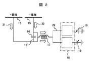
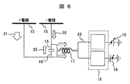
- FIG. 2 4, and 6 are diagrams schematically showing the configuration of the electrostatic chucking electrode, the DC power source, and the feed line between them in the plasma processing apparatus according to the embodiment shown in FIG. 1, and the current flowing thereover. is there.
- currents (high-frequency currents) 31 and 32 of the same direction and the same amount of high-frequency power flow into the electrodes having positive and negative polarities of the tungsten electrode 15 that is a bipolar electrostatic adsorption electrode. Shows the case.
- Reference numeral 31 denotes a high-frequency current flowing through the tungsten electrode 15 having a positive potential and the feed line connected thereto
- reference numeral 32 denotes a high-frequency current flowing through the tungsten electrode 15 having a negative potential and the feed line connected thereto.
- air-core winding inductances 17 are operated in the same manner so that when the high-frequency power flows through the inside of the coiled portion, the impedance is generated and the current of the high-frequency power is blocked from flowing. There is an effect of suppressing the generation of electric power and the flow of high-frequency electric current to the DC power supply 19. Furthermore, as in this embodiment, the two air-core winding inductances 17 on the feeder line 22 connected to the two tungsten electrodes 15 having positive and negative polarities are such that the winding axis of the coil portion of the line is It has a common (coiled) configuration.
- FIG. 3 is a diagram schematically showing the configuration of the electrostatic chucking electrode, the DC power source, and the feeder line between them according to a comparative example of the present embodiment, and the current flowing thereon.
- the capacitor 16 is not disposed on a line that connects the feeding lines 22 respectively connected to the two tungsten electrodes 15 in an AC manner.
- the high frequency power for plasma generation is an electric field in the VHF band (30 to 300 MHz in this embodiment) or higher
- the phase of the high frequency flowing into the positive electrode and the negative electrode due to the standing wave distribution in the plasma As a result, the directions of the high-frequency currents 31 and 32 flowing through the two feeder lines 22 may be different.
- the high-frequency current 31 flowing through the tungsten electrode 15 set to a positive potential and the feeder line 22 connected thereto is connected to the tungsten electrode 15 set to a negative potential and to the DC power source 19.
- the high-frequency current 32 flowing through the feeder line 22 is flowing toward the tungsten electrode 15.
- the capacitor 16 connects the feed lines 22 between the air core winding inductance 17 and the tungsten electrode 15, and is arranged in an alternating manner before the so-called air core winding inductance 17.
- the electromotive forces due to the inductance generated in the shaped parts cancel each other. For this reason, even if the air core winding inductance 17 is provided, the effect of reducing the variation of the high frequency current due to the inductance having the same characteristics as shown in FIG. 2 is impaired, and the effect of the high impedance provided in the embodiment of FIG. The success of is inhibited.
- FIG. 4 is a diagram schematically showing the configuration of the electrostatic adsorption electrode, the DC power source and the power supply line between them and the current flowing thereover in the plasma processing apparatus according to the embodiment shown in FIG.
- the high-frequency current 31 flowing through the tungsten electrode 15 having a positive potential and the feed line 22 connected thereto is directed toward the DC power source 19 and the tungsten electrode 15 having a negative potential.
- the high-frequency current 32 flowing through the feeder line 22 connected to is shown in the state of flowing toward the tungsten electrode 15.
- a high-frequency current 31 passes through a bypass line 16 ′ connected to a power supply line 22 between a tungsten electrode 15 having a positive potential and an air core winding inductance 17 as a bypass current 33 through a capacitor 16, It flows into the feed line 22 connected to the tungsten electrode 15 having a negative potential through the line 22.
- the high-frequency current 31 is bypassed by connecting the capacitor 16 and the bypass line 16 ′, the phase is different in a state where the high-frequency current 32 flows through the coiled portion of one air-core winding inductance 17.
- the high-frequency current 31 is prevented from flowing into the coiled portion of the other air-core winding inductance 17.
- the high-frequency current flowing into each of the tungsten electrodes 15 having the positive and negative potentials has the same direction and the magnitude, for example, the amplitude (difference) has a difference (potential difference). The same effect can be achieved.
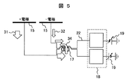
- FIG. 5 is a diagram schematically showing the configuration of an electrostatic chucking electrode, a DC power source, and a feeder line between them according to a comparative example of the present embodiment, and a current flowing thereon.
- the capacitor 16 and the bypass line 16 ′ are not connected between the two power supply lines 22, but are connected to the tungsten electrode 15 set to positive and negative potentials and to each of these.
- the high-frequency power flowing through the feeder line 22 is shown to have the same phase but different amplitude and potential difference.
- the flow directions of the high-frequency currents 31 and 32 flowing through the feeder line between each tungsten electrode 15 and the air core winding inductance are the same as those in FIG. 2, and the amplitude of the high-frequency current 31 is made larger than that of the high-frequency current 32.
- a reverse current 34 is generated via the line-to-line capacitance by the high-frequency current 31 having a large amplitude that flows through the air-core winding inductance 17.
- the reverse current 34 suppresses the action of the air core winding inductance 17 through which the high frequency current 32 having a small amplitude flows, and the impedance at the air core winding inductance 17 is lowered to increase the amount of the high frequency current 31 or the high frequency current 32 flowing. I will let you.
- the bypass line 16 ′ including the capacitor 16 is disposed and connected between the two power supply lines 22 in the previous stage of the air-core winding inductance 17.
- a part of the high-frequency current 31 having a large current is divided into the bypass line 16 ′ as the bypass current 33 and flows through the circuit, and is further connected to the feed line 22 and the bypass line 16 ′ connected to the tungsten electrode 15 having a negative potential.
- the high-frequency current 32 is joined to the air core winding inductance 17, the low-pass filter 18, and the DC power source 19. For this reason, the potential difference between the two power supply lines 22 is reduced by the amount of the capacitor 16 of the bypass line 16 ′.
- the amount of the high-frequency current flowing into the air-core winding inductance 17 is made close to an equivalent value by reducing these differences. For this reason, an inductance having the same characteristics of the air-core winding inductance 17 is generated in the coil-shaped portions of the two air-core winding inductances 17, and the amount of the high-frequency current flowing through these into the DC power source 19 is increased for each line. The action and effect that the variation is reduced is exhibited even when there is a difference in the amplitude of the current of the high-frequency power flowing through the two feeder lines 22 or there is a potential difference between the high-frequency power.
- the capacitor 16 before the air-core winding inductance 17, even if the phase and amplitude of the high-frequency current flowing into the positive and negative tungsten electrodes 15 are different from each other, the air-core winding inductance is different. It is suppressed that the impedance of 17 is impaired. As a result, the density and strength of the plasma 11 formed on the upper surface of the electrostatic adsorption film 14 of the sample table 2 due to fluctuations in the amount of high-frequency power for plasma formation flowing into the electrode for electrostatic adsorption The distribution is suppressed from variation in variation, and the sample processing yield is suppressed from being impaired.
- each of the plurality of (two in FIGS. 2, 4, and 6) tungsten electrodes 15 that are bipolar electrodes for electrostatic attraction are connected to the feed line 22 connected to each of the positive and negative potentials.
- Two air-core winding inductances 17 each having a coil-shaped portion in which the lines are wound around a common axis (made common winding) are arranged.
- the inductance of the coiled portion through which the high-frequency current flows can be increased by using a member made of a material having a magnetic permeability higher than that of the atmosphere such as a ferrite in a vacuum space or the like at the inner core portion.
- the air core winding inductance 17 is provided as an element disposed on the power feeding path connected to the electrode for electrostatic attraction.
- a material such as polytetrafluoroethylene (PTFE) such as resin having a small loss is used as a core inside the coiled line or a fixed jig for the line. It may be used.
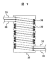
- FIG. 7 is a longitudinal sectional view schematically showing an outline of the configuration of the air core winding inductance of the embodiment shown in FIG.
- the air-core winding inductance 17 has a negative potential with a feed line (positive line) 35 connected to the tungsten electrode 15 that is set to a positive potential among the plurality of feed lines 22.
- a part of the feeder line (negative electrode side line) 36 connected to the tungsten electrode 15 to be formed is arranged on the upper and lower sides of an axis in the vertical direction of a fixed jig 37 having a cylindrical shape arranged adjacent to each other as a pair. Is wound around a cylindrical surface from the other side to the other side.
- the current of the high-frequency power for plasma formation flows in parallel around the fixed jig 37, which is a common core member, through the two feeding lines 35 and 36 of the coiled portion having such a configuration through the tungsten electrode 15. As a result, inductances with uniform characteristics are formed, and variation in the amount of high-frequency current for each line is reduced.
- the feed lines 35 and 36 of the present embodiment are arranged on the inner side of a spiral groove that extends in the vertical direction around the vertical axis on the cylindrical surface of a fixed jig 37 having a cylindrical shape made of PTFE. And is wound around the fixed jig 37 along the groove. Further, in this example, the feeder line 35 and the feeder line 36 are covered with an insulating coating 39 made of a material such as an insulating resin on the surface of the copper core wire 38.
- the capacitor 16 and the air core winding inductance 17 are preferably arranged as close as possible to the tungsten electrode 15. If the length of the feed line 22 between the capacitor 16 and the air core winding inductance 17 and the tungsten electrode 15 exceeds the wavelength of the high frequency current, the parasitic impedance of the feed line 22 affects the characteristics of the high frequency current that flows. As a result, the fluctuation becomes large, and the density and intensity of the plasma 11 formed in the processing chamber 40 above the sample stage 2 and the fluctuation of the distribution become large, and the reproducibility of the processing may be impaired.
- the length of the feed line 22 from the tungsten electrode 15 to the capacitor 16 and the air core winding inductance 17 is set to a wavelength (1.5 m) or less of the current of the high frequency power. In particular, it is 0.3 m.
- the air core winding inductance 17 has a self-resonance characteristic associated with the parasitic impedance or parasitic capacitance of the coiled portion, and has an impedance characteristic that can be represented by a parallel circuit of an inductance and a capacitance.
- an impedance characteristic that can be represented by a parallel circuit of an inductance and a capacitance.
- the self-resonant frequency of the air-core winding inductance 17 is 1.1 times or more or 0.9 times or less that of the high frequency power for plasma generation.
- the frequency of the high-frequency power is 200 MHz, it is desirable to configure the self-resonant frequency of the air-core winding inductance 17 to be around 240 MHz.
- high-frequency power for plasma generation having a high frequency can flow into the circuit of the bipolar electrostatic adsorption electrode or suppress the difference between them, and fluctuations in plasma generation and reproducibility can be reduced.
- the generation of the difference can be suppressed, and a plasma processing apparatus with improved yield can be provided.
- this invention is not limited to the above-mentioned Example, Various modifications are included.
- the above-described embodiments have been described in detail for easy understanding of the present invention, and are not necessarily limited to those having all the configurations described. Further, it is possible to add, delete, or replace another configuration for a part of a certain configuration.
- the present invention relates to a semiconductor device manufacturing apparatus, and more particularly to a plasma etching apparatus for performing an etching process of a semiconductor material using a pattern drawn by a lithography technique as a mask.
- the high frequency for plasma generation is effective for flowing into the electrostatic adsorption function unit provided in the sample setting means.
- a filter that automatically blocks is realized. Due to the effects of the present invention, it is possible to significantly suppress the reduction in process reproducibility and the occurrence of differences between apparatuses in a plasma processing apparatus using a high frequency of the VHF band or higher for plasma generation.
- Electromagnetic coil 2 ... Sample stand, 2 '... Lower electrode, 3 ... Sample, 4 ... Upper electrode, 5 ... shower plate, 6 ... Gas introduction line, 7 ... Upper electrode temperature control means, 8 ... High frequency power supply for discharge , 9... High frequency power matching unit for discharge, 10... Vacuum vessel, 11. Plasma, 12. Upper electrode insulator, 13. Insulating ring, 14 ... Electrostatic adsorption film, 15 ... Tungsten electrode, 16 ... Capacitor, 16 '... Bypass line, 17 ... Air-core winding inductance, 18 ... Low-pass filter, 19 ... DC power supply, 20 ... Bias high frequency power supply, 21 ...
Landscapes
- Physics & Mathematics (AREA)
- Engineering & Computer Science (AREA)
- Plasma & Fusion (AREA)
- Chemical & Material Sciences (AREA)
- Analytical Chemistry (AREA)
- Plasma Technology (AREA)
- Drying Of Semiconductors (AREA)
- Container, Conveyance, Adherence, Positioning, Of Wafer (AREA)
Abstract
Description
Claims (5)
- 真空容器内部に配置されその内側でプラズマが形成される処理室と、この処理室内に配置され前記プラズマを用いて処理される試料がその上に載せられる試料台と、この試料台上面を構成してその上に前記試料が載せられる誘電体製の膜内に配置され当該試料を吸着するための電力が供給されて異なる極性が形成される膜状の2つの電極と、当該2つの電極と各々の電源との間の給電路上に配置され前記2つの電極各々に接続された2つの給電線路が同じ軸回りに並列に巻かれたコイル状部分と、このコイル状部分と前記2つ電極との間において前記2つの給電線路を接続しコンデンサを備えたバイパス線路とを備えたプラズマ処理装置。
- 請求項1記載のプラズマ処理装置であって、
前記処理室内に前記プラズマを形成する電界を形成する高周波電力を供給する高周波電源を有し、前記高周波電力の周波数が30乃至300MHzの範囲内であるプラズマ処理装置。 - 請求項1または2に記載のプラズマ処理装置であって、
前記コイル状部分が内部に芯を有さないプラズマ処理装置。 - 請求項1乃至3の何れか一項に記載のプラズマ処理装置であって、
前記コイル状部分が前記2つの給電線路上であって当該線路の前記2つ電極からの距離が前記高周波電力の1波長以内に配置されたプラズマ処理装置。 - 請求項1乃至4の何れか一項に記載のプラズマ処理装置であって、
前記2つの給電線路上の前記コイル状部分と前記各々の電源との間に配置され前記高周波電力を濾過するフィルタを備えたプラズマ処理装置。
Priority Applications (5)
| Application Number | Priority Date | Filing Date | Title |
|---|---|---|---|
| JP2018511164A JP6530859B2 (ja) | 2017-03-21 | 2017-03-21 | プラズマ処理装置 |
| US15/755,338 US10825657B2 (en) | 2017-03-21 | 2017-03-21 | Plasma processing apparatus |
| PCT/JP2017/011093 WO2018173095A1 (ja) | 2017-03-21 | 2017-03-21 | プラズマ処理装置 |
| KR1020187003988A KR102056724B1 (ko) | 2017-03-21 | 2017-03-21 | 플라스마 처리 장치 |
| TW107106355A TWI701706B (zh) | 2017-03-21 | 2018-02-26 | 電漿處理裝置 |
Applications Claiming Priority (1)
| Application Number | Priority Date | Filing Date | Title |
|---|---|---|---|
| PCT/JP2017/011093 WO2018173095A1 (ja) | 2017-03-21 | 2017-03-21 | プラズマ処理装置 |
Publications (1)
| Publication Number | Publication Date |
|---|---|
| WO2018173095A1 true WO2018173095A1 (ja) | 2018-09-27 |
Family
ID=63584322
Family Applications (1)
| Application Number | Title | Priority Date | Filing Date |
|---|---|---|---|
| PCT/JP2017/011093 Ceased WO2018173095A1 (ja) | 2017-03-21 | 2017-03-21 | プラズマ処理装置 |
Country Status (5)
| Country | Link |
|---|---|
| US (1) | US10825657B2 (ja) |
| JP (1) | JP6530859B2 (ja) |
| KR (1) | KR102056724B1 (ja) |
| TW (1) | TWI701706B (ja) |
| WO (1) | WO2018173095A1 (ja) |
Cited By (2)
| Publication number | Priority date | Publication date | Assignee | Title |
|---|---|---|---|---|
| JP2022117669A (ja) * | 2021-02-01 | 2022-08-12 | 東京エレクトロン株式会社 | フィルタ回路及びプラズマ処理装置 |
| JP2023013666A (ja) * | 2021-07-16 | 2023-01-26 | 東京エレクトロン株式会社 | プラズマ処理装置及び処理方法 |
Families Citing this family (5)
| Publication number | Priority date | Publication date | Assignee | Title |
|---|---|---|---|---|
| CN111199860A (zh) * | 2018-11-20 | 2020-05-26 | 江苏鲁汶仪器有限公司 | 一种刻蚀均匀性调节装置及方法 |
| KR102593142B1 (ko) * | 2020-05-19 | 2023-10-25 | 세메스 주식회사 | 기판 처리 장치 및 그의 페라이트 코어 온도 제어 방법 |
| KR102785926B1 (ko) * | 2020-11-06 | 2025-03-26 | 세메스 주식회사 | 기판 처리 장치 |
| CN116344307A (zh) * | 2021-12-24 | 2023-06-27 | 中微半导体设备(上海)股份有限公司 | 静电卡盘系统及半导体处理设备 |
| US12573588B2 (en) * | 2024-04-02 | 2026-03-10 | Applied Materials, Inc. | Plasma processing system configured to deliver a pulsed voltage waveform |
Citations (5)
| Publication number | Priority date | Publication date | Assignee | Title |
|---|---|---|---|---|
| JPS605539A (ja) * | 1983-06-23 | 1985-01-12 | Fujitsu Ltd | プラズマ処理方法 |
| JPH03179735A (ja) * | 1989-12-07 | 1991-08-05 | Tokyo Electron Ltd | プラズマ処理装置 |
| JPH06326176A (ja) * | 1993-05-12 | 1994-11-25 | Tokyo Electron Ltd | 自己バイアス測定方法及び装置並びに静電吸着装置 |
| JP2016031955A (ja) * | 2014-07-28 | 2016-03-07 | 株式会社日立ハイテクノロジーズ | プラズマ処理装置およびプラズマ処理方法 |
| JP2016131235A (ja) * | 2015-01-09 | 2016-07-21 | 株式会社日立ハイテクノロジーズ | プラズマ処理装置およびプラズマ処理方法 |
Family Cites Families (4)
| Publication number | Priority date | Publication date | Assignee | Title |
|---|---|---|---|---|
| US5557215A (en) | 1993-05-12 | 1996-09-17 | Tokyo Electron Limited | Self-bias measuring method, apparatus thereof and electrostatic chucking apparatus |
| JP6027374B2 (ja) | 2012-09-12 | 2016-11-16 | 東京エレクトロン株式会社 | プラズマ処理装置及びフィルタユニット |
| US9779919B2 (en) * | 2015-01-09 | 2017-10-03 | Hitachi High-Technologies Corporation | Plasma processing apparatus and plasma processing method |
| JP6650593B2 (ja) * | 2017-02-17 | 2020-02-19 | パナソニックIpマネジメント株式会社 | プラズマ処理装置およびプラズマ処理方法 |
-
2017
- 2017-03-21 JP JP2018511164A patent/JP6530859B2/ja active Active
- 2017-03-21 US US15/755,338 patent/US10825657B2/en active Active
- 2017-03-21 WO PCT/JP2017/011093 patent/WO2018173095A1/ja not_active Ceased
- 2017-03-21 KR KR1020187003988A patent/KR102056724B1/ko active Active
-
2018
- 2018-02-26 TW TW107106355A patent/TWI701706B/zh active
Patent Citations (5)
| Publication number | Priority date | Publication date | Assignee | Title |
|---|---|---|---|---|
| JPS605539A (ja) * | 1983-06-23 | 1985-01-12 | Fujitsu Ltd | プラズマ処理方法 |
| JPH03179735A (ja) * | 1989-12-07 | 1991-08-05 | Tokyo Electron Ltd | プラズマ処理装置 |
| JPH06326176A (ja) * | 1993-05-12 | 1994-11-25 | Tokyo Electron Ltd | 自己バイアス測定方法及び装置並びに静電吸着装置 |
| JP2016031955A (ja) * | 2014-07-28 | 2016-03-07 | 株式会社日立ハイテクノロジーズ | プラズマ処理装置およびプラズマ処理方法 |
| JP2016131235A (ja) * | 2015-01-09 | 2016-07-21 | 株式会社日立ハイテクノロジーズ | プラズマ処理装置およびプラズマ処理方法 |
Cited By (4)
| Publication number | Priority date | Publication date | Assignee | Title |
|---|---|---|---|---|
| JP2022117669A (ja) * | 2021-02-01 | 2022-08-12 | 東京エレクトロン株式会社 | フィルタ回路及びプラズマ処理装置 |
| JP7534235B2 (ja) | 2021-02-01 | 2024-08-14 | 東京エレクトロン株式会社 | フィルタ回路及びプラズマ処理装置 |
| JP2023013666A (ja) * | 2021-07-16 | 2023-01-26 | 東京エレクトロン株式会社 | プラズマ処理装置及び処理方法 |
| JP7645732B2 (ja) | 2021-07-16 | 2025-03-14 | 東京エレクトロン株式会社 | プラズマ処理装置及び処理方法 |
Also Published As
| Publication number | Publication date |
|---|---|
| TW201843695A (zh) | 2018-12-16 |
| JP6530859B2 (ja) | 2019-06-12 |
| US10825657B2 (en) | 2020-11-03 |
| JPWO2018173095A1 (ja) | 2019-04-04 |
| TWI701706B (zh) | 2020-08-11 |
| US20200234924A1 (en) | 2020-07-23 |
| KR102056724B1 (ko) | 2019-12-17 |
| KR20180125432A (ko) | 2018-11-23 |
Similar Documents
| Publication | Publication Date | Title |
|---|---|---|
| JP6530859B2 (ja) | プラズマ処理装置 | |
| JP5800547B2 (ja) | プラズマ処理装置及びプラズマ処理方法 | |
| JP6027374B2 (ja) | プラズマ処理装置及びフィルタユニット | |
| US9530619B2 (en) | Plasma processing apparatus and filter unit | |
| KR101974268B1 (ko) | 플라즈마 처리 장치 | |
| CN104994676B (zh) | 等离子体处理装置 | |
| JP5723130B2 (ja) | プラズマ処理装置 | |
| US9218943B2 (en) | Plasma processing apparatus and plasma processing method | |
| JP5851682B2 (ja) | プラズマ処理装置 | |
| JP5800532B2 (ja) | プラズマ処理装置及びプラズマ処理方法 | |
| US6265031B1 (en) | Method for plasma processing by shaping an induced electric field | |
| US20150243486A1 (en) | Plasma processing apparatus | |
| US6850012B2 (en) | Plasma processing apparatus | |
| TWI661465B (zh) | 電漿處理裝置 | |
| JP7422077B2 (ja) | 高電力無線周波数の螺旋コイルフィルタ | |
| JP6053881B2 (ja) | プラズマ処理装置 | |
| JP6062461B2 (ja) | プラズマ処理装置 | |
| JP6097317B2 (ja) | プラズマ処理方法 | |
| WO2020121588A1 (ja) | プラズマ処理装置 | |
| JP2016046357A (ja) | プラズマ処理装置 | |
| JP2015159118A (ja) | プラズマ処理装置 |
Legal Events
| Date | Code | Title | Description |
|---|---|---|---|
| ENP | Entry into the national phase |
Ref document number: 20187003988 Country of ref document: KR Kind code of ref document: A |
|
| ENP | Entry into the national phase |
Ref document number: 2018511164 Country of ref document: JP Kind code of ref document: A |
|
| 121 | Ep: the epo has been informed by wipo that ep was designated in this application |
Ref document number: 17901392 Country of ref document: EP Kind code of ref document: A1 |
|
| NENP | Non-entry into the national phase |
Ref country code: DE |
|
| 122 | Ep: pct application non-entry in european phase |
Ref document number: 17901392 Country of ref document: EP Kind code of ref document: A1 |