WO2018168174A1 - 表示装置および表示装置の駆動方法 - Google Patents
表示装置および表示装置の駆動方法 Download PDFInfo
- Publication number
- WO2018168174A1 WO2018168174A1 PCT/JP2018/000684 JP2018000684W WO2018168174A1 WO 2018168174 A1 WO2018168174 A1 WO 2018168174A1 JP 2018000684 W JP2018000684 W JP 2018000684W WO 2018168174 A1 WO2018168174 A1 WO 2018168174A1
- Authority
- WO
- WIPO (PCT)
- Prior art keywords
- pixel
- terminal
- switch
- light emitting
- emitting element
- Prior art date
- Legal status (The legal status is an assumption and is not a legal conclusion. Google has not performed a legal analysis and makes no representation as to the accuracy of the status listed.)
- Ceased
Links
Images


Classifications
-
- G—PHYSICS
- G09—EDUCATION; CRYPTOGRAPHY; DISPLAY; ADVERTISING; SEALS
- G09G—ARRANGEMENTS OR CIRCUITS FOR CONTROL OF INDICATING DEVICES USING STATIC MEANS TO PRESENT VARIABLE INFORMATION
- G09G3/00—Control arrangements or circuits, of interest only in connection with visual indicators other than cathode-ray tubes
- G09G3/20—Control arrangements or circuits, of interest only in connection with visual indicators other than cathode-ray tubes for presentation of an assembly of a number of characters, e.g. a page, by composing the assembly by combination of individual elements arranged in a matrix no fixed position being assigned to or needed to be assigned to the individual characters or partial characters
- G09G3/22—Control arrangements or circuits, of interest only in connection with visual indicators other than cathode-ray tubes for presentation of an assembly of a number of characters, e.g. a page, by composing the assembly by combination of individual elements arranged in a matrix no fixed position being assigned to or needed to be assigned to the individual characters or partial characters using controlled light sources
- G09G3/30—Control arrangements or circuits, of interest only in connection with visual indicators other than cathode-ray tubes for presentation of an assembly of a number of characters, e.g. a page, by composing the assembly by combination of individual elements arranged in a matrix no fixed position being assigned to or needed to be assigned to the individual characters or partial characters using controlled light sources using electroluminescent panels
- G09G3/32—Control arrangements or circuits, of interest only in connection with visual indicators other than cathode-ray tubes for presentation of an assembly of a number of characters, e.g. a page, by composing the assembly by combination of individual elements arranged in a matrix no fixed position being assigned to or needed to be assigned to the individual characters or partial characters using controlled light sources using electroluminescent panels semiconductive, e.g. using light-emitting diodes [LED]
- G09G3/3208—Control arrangements or circuits, of interest only in connection with visual indicators other than cathode-ray tubes for presentation of an assembly of a number of characters, e.g. a page, by composing the assembly by combination of individual elements arranged in a matrix no fixed position being assigned to or needed to be assigned to the individual characters or partial characters using controlled light sources using electroluminescent panels semiconductive, e.g. using light-emitting diodes [LED] organic, e.g. using organic light-emitting diodes [OLED]
- G09G3/3225—Control arrangements or circuits, of interest only in connection with visual indicators other than cathode-ray tubes for presentation of an assembly of a number of characters, e.g. a page, by composing the assembly by combination of individual elements arranged in a matrix no fixed position being assigned to or needed to be assigned to the individual characters or partial characters using controlled light sources using electroluminescent panels semiconductive, e.g. using light-emitting diodes [LED] organic, e.g. using organic light-emitting diodes [OLED] using an active matrix
- G09G3/3233—Control arrangements or circuits, of interest only in connection with visual indicators other than cathode-ray tubes for presentation of an assembly of a number of characters, e.g. a page, by composing the assembly by combination of individual elements arranged in a matrix no fixed position being assigned to or needed to be assigned to the individual characters or partial characters using controlled light sources using electroluminescent panels semiconductive, e.g. using light-emitting diodes [LED] organic, e.g. using organic light-emitting diodes [OLED] using an active matrix with pixel circuitry controlling the current through the light-emitting element
-
- G—PHYSICS
- G09—EDUCATION; CRYPTOGRAPHY; DISPLAY; ADVERTISING; SEALS
- G09G—ARRANGEMENTS OR CIRCUITS FOR CONTROL OF INDICATING DEVICES USING STATIC MEANS TO PRESENT VARIABLE INFORMATION
- G09G3/00—Control arrangements or circuits, of interest only in connection with visual indicators other than cathode-ray tubes
- G09G3/20—Control arrangements or circuits, of interest only in connection with visual indicators other than cathode-ray tubes for presentation of an assembly of a number of characters, e.g. a page, by composing the assembly by combination of individual elements arranged in a matrix no fixed position being assigned to or needed to be assigned to the individual characters or partial characters
- G09G3/22—Control arrangements or circuits, of interest only in connection with visual indicators other than cathode-ray tubes for presentation of an assembly of a number of characters, e.g. a page, by composing the assembly by combination of individual elements arranged in a matrix no fixed position being assigned to or needed to be assigned to the individual characters or partial characters using controlled light sources
- G09G3/30—Control arrangements or circuits, of interest only in connection with visual indicators other than cathode-ray tubes for presentation of an assembly of a number of characters, e.g. a page, by composing the assembly by combination of individual elements arranged in a matrix no fixed position being assigned to or needed to be assigned to the individual characters or partial characters using controlled light sources using electroluminescent panels
- G09G3/32—Control arrangements or circuits, of interest only in connection with visual indicators other than cathode-ray tubes for presentation of an assembly of a number of characters, e.g. a page, by composing the assembly by combination of individual elements arranged in a matrix no fixed position being assigned to or needed to be assigned to the individual characters or partial characters using controlled light sources using electroluminescent panels semiconductive, e.g. using light-emitting diodes [LED]
- G09G3/3208—Control arrangements or circuits, of interest only in connection with visual indicators other than cathode-ray tubes for presentation of an assembly of a number of characters, e.g. a page, by composing the assembly by combination of individual elements arranged in a matrix no fixed position being assigned to or needed to be assigned to the individual characters or partial characters using controlled light sources using electroluminescent panels semiconductive, e.g. using light-emitting diodes [LED] organic, e.g. using organic light-emitting diodes [OLED]
- G09G3/3266—Details of drivers for scan electrodes
-
- G—PHYSICS
- G09—EDUCATION; CRYPTOGRAPHY; DISPLAY; ADVERTISING; SEALS
- G09G—ARRANGEMENTS OR CIRCUITS FOR CONTROL OF INDICATING DEVICES USING STATIC MEANS TO PRESENT VARIABLE INFORMATION
- G09G2300/00—Aspects of the constitution of display devices
- G09G2300/04—Structural and physical details of display devices
- G09G2300/0421—Structural details of the set of electrodes
- G09G2300/0426—Layout of electrodes and connections
-
- G—PHYSICS
- G09—EDUCATION; CRYPTOGRAPHY; DISPLAY; ADVERTISING; SEALS
- G09G—ARRANGEMENTS OR CIRCUITS FOR CONTROL OF INDICATING DEVICES USING STATIC MEANS TO PRESENT VARIABLE INFORMATION
- G09G2300/00—Aspects of the constitution of display devices
- G09G2300/08—Active matrix structure, i.e. with use of active elements, inclusive of non-linear two terminal elements, in the pixels together with light emitting or modulating elements
- G09G2300/0809—Several active elements per pixel in active matrix panels
- G09G2300/0842—Several active elements per pixel in active matrix panels forming a memory circuit, e.g. a dynamic memory with one capacitor
- G09G2300/0852—Several active elements per pixel in active matrix panels forming a memory circuit, e.g. a dynamic memory with one capacitor being a dynamic memory with more than one capacitor
-
- G—PHYSICS
- G09—EDUCATION; CRYPTOGRAPHY; DISPLAY; ADVERTISING; SEALS
- G09G—ARRANGEMENTS OR CIRCUITS FOR CONTROL OF INDICATING DEVICES USING STATIC MEANS TO PRESENT VARIABLE INFORMATION
- G09G2300/00—Aspects of the constitution of display devices
- G09G2300/08—Active matrix structure, i.e. with use of active elements, inclusive of non-linear two terminal elements, in the pixels together with light emitting or modulating elements
- G09G2300/0809—Several active elements per pixel in active matrix panels
- G09G2300/0842—Several active elements per pixel in active matrix panels forming a memory circuit, e.g. a dynamic memory with one capacitor
- G09G2300/0861—Several active elements per pixel in active matrix panels forming a memory circuit, e.g. a dynamic memory with one capacitor with additional control of the display period without amending the charge stored in a pixel memory, e.g. by means of additional select electrodes
-
- G—PHYSICS
- G09—EDUCATION; CRYPTOGRAPHY; DISPLAY; ADVERTISING; SEALS
- G09G—ARRANGEMENTS OR CIRCUITS FOR CONTROL OF INDICATING DEVICES USING STATIC MEANS TO PRESENT VARIABLE INFORMATION
- G09G2310/00—Command of the display device
- G09G2310/02—Addressing, scanning or driving the display screen or processing steps related thereto
- G09G2310/0243—Details of the generation of driving signals
- G09G2310/0251—Precharge or discharge of pixel before applying new pixel voltage
-
- G—PHYSICS
- G09—EDUCATION; CRYPTOGRAPHY; DISPLAY; ADVERTISING; SEALS
- G09G—ARRANGEMENTS OR CIRCUITS FOR CONTROL OF INDICATING DEVICES USING STATIC MEANS TO PRESENT VARIABLE INFORMATION
- G09G2310/00—Command of the display device
- G09G2310/02—Addressing, scanning or driving the display screen or processing steps related thereto
- G09G2310/0262—The addressing of the pixel, in a display other than an active matrix LCD, involving the control of two or more scan electrodes or two or more data electrodes, e.g. pixel voltage dependent on signals of two data electrodes
Definitions
- the present invention relates to a display device and a display device driving method.
- An organic electroluminescence display device (hereinafter referred to as an EL display device) includes a plurality of transistors, capacitor elements, and organic light-emitting elements (hereinafter referred to as light-emitting elements) included in each of a plurality of pixels formed on a substrate. ). Each pixel is driven by a signal that controls the pixel. By controlling the driving of the transistor included in each pixel by a signal, a current supplied to the light-emitting element (hereinafter referred to as a light-emitting current) is controlled, and the display device can display an image.
- a light-emitting current a current supplied to the light-emitting element
- the EL display device In order to realize high definition, it is necessary to reduce the pixel size.
- an EL display device for example, by using a color filter corresponding to the three primary colors of RGB and a white light emitting element, color display becomes possible, and there is no need to separate each color of RGB, and it is necessary to worry about positional accuracy. Therefore, a high-definition display device can be provided.
- the organic material of the light emitting layer is applied with high definition so that the pixel size can be reduced.
- Technology to deploy has been developed.
- the driving method of the EL display device is also required to be adapted to the high definition of the display device.
- Patent Document 1 discloses a pixel circuit including two transistors, two capacitors, and one light emitting element, a display device including the pixel circuit, and a driving method.
- Patent Document 2 discloses a pixel circuit including three transistors, three capacitors, and one light emitting element, a display device including the pixel circuit, and a driving method.
- a pixel included in an EL display device requires a plurality of transistors and capacitors.
- the EL display device can be expected to have high definition.
- the pixel size is reduced, and the size of each element must be reduced. Therefore, the size of the capacitor provided in one pixel is also reduced, and the capacitance value of the capacitor is also reduced. That is, the maximum value of the storage capacity that can be stored in one pixel is reduced. As a result, the maximum value of the light emission current that can be supplied to the light emitting element is reduced, which may cause a reduction in dynamic range and image quality.
- one embodiment of the present invention is to provide a display device having a large light emission current and a high dynamic range.
- One embodiment of the present invention is a display device, which includes a first light emitting element having a first pixel electrode and a common electrode, an input / output terminal, and one of the input / output terminals is connected to the first pixel electrode.
- a first pixel including a driving transistor; a second pixel including a second light emitting element adjacent to the first pixel and having a second pixel electrode and a common electrode; and the first pixel electrode and the second pixel.
- the pixel electrode is connected via a first switch.
- One embodiment of the present invention is a method for driving a display device, and in a first pixel including a first light emitting element, one of input / output terminals is electrically connected to one terminal of the first light emitting element.
- a second driving transistor in which one of input / output terminals is electrically connected to one terminal of the second light emitting element in the second pixel including the second light emitting element adjacent to the gate of the first driving transistor and the second pixel
- An initialization potential is applied to the gate of the first driving transistor, a power supply voltage is applied to the other input / output terminal of the first driving transistor, and one terminal of the first light emitting element and one terminal of the second light emitting element are electrically connected to each other.
- a gate voltage corresponding to the video signal input to the first pixel is applied to the gate of the first driving transistor, the electrical connection between the first light emitting element and the second light emitting element is interrupted, Power supply voltage is marked on the other side of one drive transistor In a state, providing a current corresponding to the gate voltage to the first light emitting element.
- One embodiment of the present invention includes a first pixel and a second pixel adjacent to the first pixel, wherein the first pixel and the second pixel are a drive transistor, a light emitting element, an additional capacitor, A second switch, a capacitive element, a fourth switch, a fifth switch, and a power supply line, and includes one input / output terminal of the drive transistor, one terminal of the light emitting element, and one terminal of the additional capacitor.
- the second switch is connected to the gate of the driving transistor, one terminal of the capacitor is electrically connected to the gate of the driving transistor, and one terminal of the fourth switch is The other terminal of the capacitor element, one terminal of the light emitting element, and one terminal of the additional capacitor are electrically connected, and the other terminal of the fifth switch is connected to the other input / output terminal of the drive transistor, Electrically connected, the fifth switch One terminal of the H is electrically connected to the power supply line, and is included in one terminal of the light emitting element included in the first pixel, one terminal of the additional capacitor included in the first pixel, and the second pixel.
- a display device having a first switch that electrically connects one terminal of a light emitting element to be connected to one terminal of an additional capacitor included in the second pixel, the driving method of the light emitting element of the first pixel
- One terminal and one terminal of the additional capacitor of the first pixel, and one terminal of the light emitting element of the second pixel and one terminal of the additional capacitor of the second pixel are turned on. Electrically connected to the gate of the drive transistor of the first pixel by turning on the second switch of the first pixel to apply the initialization potential to the gate of the drive transistor of the second pixel.
- the second switch of the first pixel is turned off, and the electrical connection between the light emitting element of the first pixel and the additional capacitor of the first pixel and the light emitting element of the second pixel and the additional capacitor of the second pixel is performed.
- the current corresponding to the gate voltage of the driving transistor of the first pixel is cut off and a power supply voltage is applied to the other input / output terminal of the driving transistor of the first pixel. This is applied to a light emitting element of one pixel.
- One embodiment of the present invention includes a first pixel and a second pixel adjacent to the first pixel, wherein the first pixel and the second pixel are a drive transistor, a light emitting element, an additional capacitor, Including a second switch, a capacitive element, a third switch, a fourth switch, a fifth switch, and a power supply line, one of the input / output terminals of the driving transistor, one terminal of the light emitting element, and an additional One terminal of the capacitor is electrically connected, the second switch is connected to the gate of the driving transistor, and one terminal of the capacitor is electrically connected to the gate of the driving transistor, and the third switch One terminal of the fourth transistor is electrically connected to the gate of the driving transistor and one terminal of the capacitor element, and one terminal of the fourth switch is connected to the other terminal of the capacitor element and one terminal of the light emitting element.
- One terminal of additional capacity The other terminal of the fifth switch is electrically connected to the other input / output terminal of the driving transistor, and one terminal of the fifth switch is electrically connected to the power line. , One terminal of the light emitting element included in the first pixel, one terminal of the additional capacitor included in the first pixel, one terminal of the light emitting element included in the second pixel, and an additional element included in the second pixel.
- a driving method of a display device having a first switch that electrically connects one terminal of a capacitor, wherein one terminal of a light emitting element of the first pixel and one terminal of an additional capacitor of the first pixel; One terminal of the light emitting element of the second pixel and one terminal of the additional capacitor of the second pixel are electrically connected by turning on the first switch, and connected to the gate of the driving transistor of the first pixel.
- the third switch of the first pixel is turned off, and the light emitting element of the first pixel and the light emitting element of the second pixel are connected to the gate of the driving transistor of the first pixel.
- 2 switch on
- the second switch of the first pixel is turned off, the light emitting element of the first pixel, the additional capacitor of the first pixel, the light emitting element of the second pixel, and the second
- the electrical connection with the additional capacitor of the pixel is cut off by turning off the first switch, and the power supply voltage is applied to the other input / output terminal of the driving transistor of the first pixel, and the first pixel A current corresponding to the gate voltage of the driving transistor is applied to the light emitting element of the first pixel.
- One embodiment of the present invention includes a first pixel and a second pixel adjacent to the first pixel, wherein the first pixel and the second pixel are a driving transistor, a light emitting element, an additional capacitor, and the like, respectively.
- the one terminal of the additional capacitor is electrically connected
- the second switch is connected to the gate of the drive transistor
- the one terminal of the capacitor element is electrically connected to the gate of the drive transistor
- the fourth One terminal of the switch is electrically connected to the other terminal of the fifth switch and one terminal of the sixth switch, and the other terminal of the sixth switch is connected to the other input / output terminal of the driving transistor
- Electrically connected, 5th One terminal of the switch is electrically connected to the power supply line, and includes one terminal of the light emitting element included in the first pixel,
- a display device having a first switch that electrically connects one terminal of a light emitting element to be connected to one terminal of an additional capacitor included in the second pixel, the driving method of the light emitting element of the first pixel
- One terminal and one terminal of the additional capacitor of the first pixel, and one terminal of the light emitting element of the second pixel and one terminal of the additional capacitor of the second pixel are turned on.
- Electrically connected to the gate of the drive transistor of the first pixel by turning on the second switch of the first pixel to apply the initialization potential to the gate of the drive transistor of the second pixel.
- the second switch of the second pixel is turned on.
- the initialization potential is applied, and the fifth switch of the first pixel is turned off to one of the input / output terminals of the driving transistor of the first pixel, and the fourth switch and the sixth switch of the first pixel are turned off.
- the reset potential simultaneously by turning on the first state, the fourth switch of the first pixel is turned off, and the fifth switch of the first pixel is turned on, whereby the first pixel A power supply voltage is applied to the other input / output terminal of the driving transistor of the first pixel, and the potential between one of the input / output terminals of the driving transistor of the first pixel and the gate is set as the threshold voltage of the driving transistor of the first pixel.
- the light emitting element of the first pixel and the light emitting element of the second pixel are connected, and the gate of the driving transistor of the first pixel
- the first pixel By turning on the second switch, a voltage corresponding to the video signal is applied, the second switch of the first pixel is turned off, the light emitting element of the first pixel, the additional capacitor of the first pixel, and the second pixel
- the electrical connection between the light emitting element and the additional capacitor of the second pixel was cut off by turning off the first switch, and a power supply voltage was applied to the other input / output terminal of the driving transistor of the first pixel. In this state, a current corresponding to the gate voltage of the driving transistor of the first pixel is applied to the light emitting element of the first pixel.
- One embodiment of the present invention includes a first pixel and a second pixel adjacent to the first pixel, wherein the first pixel and the second pixel are a drive transistor, a light emitting element, an additional capacitor, A second switch; a capacitor; a third switch; a fourth switch; a fifth switch; a sixth switch; and a power supply line.
- One of the input / output terminals of the drive transistor and one of the light emitting elements And the one terminal of the additional capacitor are electrically connected, the second switch is connected to the gate of the driving transistor, and one terminal of the capacitive element is electrically connected to the gate of the driving transistor.
- One terminal of the third switch is electrically connected to the gate of the driving transistor and one terminal of the capacitive element, and one terminal of the fourth switch is electrically connected to the other terminal of the fifth switch, One terminal of 6 switches The other terminal of the sixth switch is electrically connected to the other input / output terminal of the drive transistor, and one terminal of the fifth switch is electrically connected to the power supply line.
- a driving method of a display device having a first switch that electrically connects one terminal of a capacitor, wherein one terminal of a light emitting element of the first pixel and one terminal of an additional capacitor of the first pixel; One terminal of the light emitting element of the second pixel and one terminal of the additional capacitor of the second pixel are electrically connected by turning on the first switch, and connected to the gate of the driving transistor of the first pixel.
- the third switch of the second pixel is turned on to the gate of the driving transistor of the second pixel, so that the initialization potential is applied and the input / output terminal of the driving transistor of the first pixel
- the reset potential is applied and the fourth switch of the first pixel is turned on.
- the power supply voltage is applied to the other input / output terminal of the drive transistor of the first pixel, and one of the input / output terminals of the drive transistor of the first pixel is applied.
- the potential between the gate and the gate is the threshold voltage of the driving transistor of the first pixel, the third switch of the first pixel is turned off, and the light emitting element of the first pixel and the light emitting element of the second pixel are connected Then, driving the first pixel
- a voltage corresponding to the video signal is applied, the second switch of the first pixel is turned off, and the light emitting element of the first pixel and the first switch
- the electrical connection between the additional capacitor of one pixel and the light emitting element of the second pixel and the additional capacitor of the second pixel is cut off by turning off the first switch, and input / output of the driving transistor of the first pixel In a state where the power supply voltage is applied to the other terminal, a current corresponding to the gate voltage of the driving transistor of the first pixel is applied to the light emitting element of the first pixel.
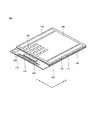
- FIG. 1 is a schematic perspective view of a display device according to an embodiment of the present invention.
- 1 is a schematic plan view of a display device according to an embodiment of the present invention.
- 1 is a circuit diagram of a pixel included in a display device according to an embodiment of the present invention.
- 4 is a timing chart of pixels included in a display device according to an embodiment of the present invention.
- 4 is a timing chart of pixels included in a display device according to an embodiment of the present invention.
- FIG. 6 is a schematic diagram illustrating a state of a pixel included in a display device according to an embodiment of the present invention for each period. 4 is a timing chart of pixels included in a display device according to an embodiment of the present invention.
- FIG. 1 is a schematic perspective view of a display device according to an embodiment of the present invention.
- 1 is a schematic plan view of a display device according to an embodiment of the present invention.
- 1 is a circuit diagram of a pixel included in a display device according to
- FIG. 6 is a schematic diagram illustrating a state of a pixel included in a display device according to an embodiment of the present invention for each period.
- 1 is a circuit diagram of a pixel included in a display device according to an embodiment of the present invention.
- 4 is a timing chart of pixels included in a display device according to an embodiment of the present invention.
- 1 is a circuit diagram of a pixel included in a display device according to an embodiment of the present invention.
- 4 is a timing chart of pixels included in a display device according to an embodiment of the present invention.
- 1 is a circuit diagram of a pixel included in a display device according to an embodiment of the present invention.
- 4 is a timing chart of pixels included in a display device according to an embodiment of the present invention.
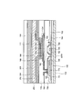
- 1 is a schematic cross-sectional view of a pixel included in a display device according to an embodiment of the present invention.
- the first substrate described in this specification has at least one planar main surface, and each element such as an insulating layer, a semiconductor layer, and a conductive layer, or a transistor and a display element is formed on the one main surface.
- each element such as an insulating layer, a semiconductor layer, and a conductive layer, or a transistor and a display element is formed on the one main surface.
- an EL display device has a plurality of pixels formed on a substrate.
- Each of the plurality of pixels includes a driving transistor, a capacitor element, a light emitting element, and an additional capacitor included in the light emitting element.
- the additional capacitance included in the light emitting element includes, for example, a case where the light emitting element itself having a diode characteristic also has a capacitance component.
- Each pixel supplies a light-emitting current to the light-emitting element by controlling the driving of the driving transistor with a signal, and the display device can display an image when the light-emitting element emits light. That is, the light emitting element becomes brighter or darker depending on the magnitude of the light emission current.
- the magnitude of the light emission current depends on the amount of current that the drive transistor flows to the light emitting element. More specifically, a charge corresponding to the amount of current flowing through the drive transistor is stored in the capacitor element and the additional capacitor, and the magnitude of the light emission current depends on the amount of the stored charge.
- the capacitance value of the capacitor or the additional capacitor is increased, the maximum value of the light emission current that can be supplied to the light emitting element can be increased without increasing the voltage applied to the capacitor or the additional capacitor.
- a capacitance value larger than the capacitance value of the pixel in other words, the capacitance element included in the pixel or the capacitance value of the additional capacitor is ensured in the light-emitting element.
- the maximum value of the light emission current that can be supplied can be increased. Further, since the display device of the present invention can increase the maximum value of the light emission current, the dynamic range of the pixel can be widened. Specifically, in a plurality of pixels included in the display device, before the light emitting element of the first pixel emits light, a light emitting element electrically connected to the driving transistor of the first pixel and an additional capacitor included in the light emitting element The light emitting element included in the second pixel adjacent to the first pixel and the additional capacitor included in the light emitting element are electrically connected by the capacitance control transistor of the first pixel.
- the driving transistor is electrically connected to the power supply line, and a video signal of the first pixel is supplied to the driving transistor of the first pixel, so that a current flows through the driving transistor of the first pixel, which corresponds to the flowing current value.
- Charge is stored in each additional capacity.
- the maximum value of the charge that can be stored based on the video signal of the first pixel can be increased by the amount of additional capacitance of the adjacent pixel that is used to hold the charge, as compared with the conventional case. That is, a large light emission current can be supplied to the light emitting element included in the first pixel. Therefore, according to the present invention, it is possible to provide a display device capable of securing a large light emission current when the pixel emits light, and to provide a display device having a pixel with a wide dynamic range.
- FIG. 1 is a schematic perspective view of a display device 100 according to an embodiment of the present invention.
- the display device 100 includes a first substrate 102, a filler 111, and a second substrate 104.
- the first surface of the first substrate 102 includes a display region 106, a scanning signal line driver circuit 118, a video signal line driver circuit (driver IC) 120, a control circuit 122, and a terminal region 114 having a plurality of terminal electrodes 116.
- the display device 100 may have a structure in which the second substrate 104 is not provided. For example, a structure in which a protective film is bonded to a side where the display region 106 of the first substrate 102 is positioned or a structure in which a circularly polarizing plate is bonded may be used.
- the display area 106 has a plurality of pixels 108.
- the plurality of pixels 108 are arranged along one direction and a direction intersecting with one direction.
- the number of pixels 108 arranged is arbitrary. For example, n pixels 108 are arranged in the row direction and m pixels 108 are arranged in the column direction. n and m are each a natural number of 2 or more.
- a plurality of terminal electrodes 116 are connected to a display substrate 100 and a device that outputs a video signal, a timing signal for controlling operations of the scanning signal line driver circuit 118 and the video signal line driver circuit 120, and the power source (see FIG. Not shown) is connected.
- the wiring board is, for example, a flexible printed circuit board (FPC).
- FPC flexible printed circuit board
- Each of the plurality of pixels 108 can be provided with a plurality of subpixels.
- one pixel includes three sub-pixels, and the three sub-pixels include a sub-pixel including a display element corresponding to red (R), a sub-pixel including a display element corresponding to green (G), It consists of a sub-pixel provided with a display element corresponding to blue (B).
- a color display device can be provided by supplying multi-level voltages or currents of, for example, 256 levels to each of the three sub-pixels, in other words, by inputting video signals of 256 gradations. .
- One sub-pixel may be simply referred to as a pixel.
- a display device in which one pixel includes one display element and can perform monochrome display or white and black gradation display can be provided.
- the arrangement of the plurality of pixels 108 is not limited, and a stripe arrangement, a delta arrangement, or the like can be employed.
- the display element provided in the pixel 108 is a light emitting element will be described.
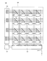
- FIG. 2 is a schematic plan view of the display device 100 according to an embodiment of the invention.
- the display device 100 is an active matrix EL display device. Each pixel 108 has a light emitting element.
- a video signal, a timing signal for controlling the operation of the circuit, and power are supplied to the control circuit 122 through the plurality of terminal electrodes 116 shown in FIG.
- the control circuit 122 supplies each signal and power supply voltage to the scanning signal line driving circuit 118 and the video signal line driving circuit 120.
- the control circuit 122 generates a new signal or power supply voltage from each signal or power supply voltage using a logic circuit (not shown) or a voltage generation circuit (not shown) included in the control circuit 122, and scan signal line driving.
- the signal may be supplied to the circuit 118 or the video signal line driver circuit 120.
- the position where the control circuit 122 is disposed is not limited to the first substrate 102 shown in FIG.
- the control circuit 122 may be located on a wiring board connected to the terminal electrode 116.
- the scanning signal line driver circuit 118 and the video signal line driver circuit 120 drive the light emitting element included in the pixel 108 using each signal and power supply voltage supplied from the control circuit and cause the light emitting element to emit light, thereby displaying the display region.
- 106 plays a role of displaying an image.
- the scanning signal line driving circuit 118 supplies a scanning signal to the plurality of pixels 108 located in the n-th row configured in the display region 106 via the scanning signal line SG (n) in common, and the control line RG ( The control signal is supplied via n), the emission control signal is supplied via the emission control signal line BG (n), and the capacitance control signal is supplied via the capacitance control signal line EG (n).
- the video signal line driving circuit 120 outputs a video signal and an initialization signal to the plurality of pixels 108 in the m-th column configured in the display area 106 in common via the video signal line SL (m). It is configured to be supplied in splits.
- the potential of the video signal is denoted as Vsig (m)
- the potential of the initialization signal is denoted as Vini. Vini may be called an initialization potential.
- the video signal is determined according to video data displayed in the display area 106, and its potential Vsig (m) is adjusted by a correction method described later.
- the potential Vini of the initialization signal can be a fixed potential.
- the video signal line drive circuit 120 is further configured to give a bias signal to a plurality of pixels located in the m-th column via the bias line VL shown in FIG.
- the potential of the bias signal is denoted as Vrst. Note that an example in which the potential Vrst of the bias signal is a fixed potential is shown, but the potential of the bias signal may vary with time.
- the video signal line driving circuit 120 is further configured to supply a high potential and a low potential to each pixel 108 via the high potential power supply wiring PVDD.
- a high potential supplied from the high potential power supply wiring PVDD is referred to as VDD_H, and a low potential is referred to as VDD_L.
- VDD_H A high potential supplied from the high potential power supply wiring PVDD
- VDD_L a low potential
- a common electrode provided in common for the plurality of pixels 108 and connected to the low potential power wiring PVSS is disposed in the display region 106.
- the video signal line driving circuit 120 is configured to supply a fixed potential VSS to the common electrode.
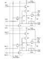
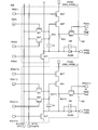
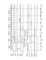
- FIG. 3 is a pixel circuit diagram 300 included in the pixel 108 according to an embodiment of the present invention.
- a pixel circuit diagram 300 shown in FIG. 3 shows two pixels 108 arranged in an n-row and m-column and an n + 1 row and m-column arranged in the display area 106.
- Each of the two pixels 108 shown in FIG. 3 includes one light emitting element OLED. Therefore, the two pixels 108 illustrated in FIG. 3 may be two adjacent sub-pixels.
- the pixel 108 includes a capacitance control transistor ECT (first switch), a selection transistor SST (second switch), a driving transistor DRT, a selection transistor SST (third switch), and an initialization transistor RST (fourth switch).
- Switch a light emission control transistor BCT (fifth switch), a capacitor element Cs, a light emitting element OLED, and an additional capacitor Cel.
- Each of these transistors has a gate and a pair of terminals (an input / output terminal, a source electrode and a drain electrode) including a first terminal and a second terminal, and the capacitor Cs has a pair of terminals (a first terminal and a first terminal).
- the additional capacitor Cel has a pair of terminals (a first terminal and a second terminal).
- FIG. 2 shows an example in which the additional capacitor Cel is provided in parallel with the light emitting element OLED, but the present invention is not limited to this.
- the additional capacitor Cel may be a parasitic capacitance of the light emitting element OLED, or may include a capacitive element provided in parallel with the light emitting element OLED and a parasitic capacitance of the light emitting element OLED.
- the driving transistor DRT has a role of causing the light emitting element OLED to emit light by causing a current to flow through the light emitting element OLED based on the input video signal.
- the selection transistor SST has a role of supplying a video signal and an initialization signal to the driving transistor DRT.
- the initialization transistor RST has a role of supplying a bias signal to the driving transistor DRT, the light emitting element OLED, and the additional capacitor Cel, and initializing a circuit included in each pixel 108.
- the light emission control transistor BCT controls connection / disconnection of the drive transistor DRT and the high potential power supply wiring PVDD. That is, the light emission control transistor BCT has a role of controlling light emission and non-light emission of the light emitting element OLED.
- the capacitance control transistor ECT includes the light emitting element OLED and the additional capacitor Cel included in the pixel, for example, the pixel 108 positioned in the n row and m column, and the light emission included in the pixel adjacent to the pixel, for example, the pixel 108 positioned in the n + 1 row and m column.
- the element OLED and the additional capacitor Cel are electrically connected to increase the capacitance value and to increase the maximum amount of current that can be supplied to the light emitting element of the pixel.
- the capacitive element Cs maintains a potential corresponding to the threshold value of the drive transistor DRT and maintains a potential input to the gate of the drive transistor DRT so that the pixel 108 emits light, that is, an input video signal is described in detail.
- the light emitting element OLED has a diode characteristic and includes a pixel electrode, the above-described common electrode, and a light emitting layer (EL layer, organic layer) positioned between the pixel electrode and the common electrode.
- the additional capacitor Cel is a capacitor included in the light emitting element OLED. The video signal input by the additional capacitor Cel and the capacitor element Cs may be held.
- the gate of the selection transistor SST is electrically connected to the scanning signal line SG (n), the first terminal is electrically connected to the video signal line SL (m), and the second terminal is the gate of the driving transistor DRT.
- the first terminal of the drive transistor DRT is electrically connected to the second terminal of the light emission control transistor BCT, the second terminal is the input terminal (or pixel electrode) of the light emitting element OLED, and the second terminal of the initialization transistor RST.
- the second terminal and the second terminal of the storage capacitor Cs are electrically connected.
- the gate of the light emission control transistor BCT is electrically connected to the light emission control signal line BG (n), and the first terminal is electrically connected to the high potential power supply wiring PVDD.
- the first terminal of the additional capacitor Cel is electrically connected to the second terminal of the drive transistor DRT, and the second terminal of the additional capacitor Cel is electrically connected to the low potential power supply line PVSS.
- the output terminal (or common electrode) of the light emitting element OLED is electrically connected to the low potential power wiring PVSS.
- a fixed potential VSS is applied to the low potential power wiring PVSS.
- the fixed potential VSS only needs to be a fixed potential lower than the low potential VDD_L, and can be, for example, a ground potential.
- the first terminal of the initialization transistor RST is electrically connected to the bias line VL, and the gate is electrically connected to the control line RG (n).
- the gate of the capacitance control transistor ECT is electrically connected to the capacitance control signal line EG (n), the first terminal is the second terminal of the capacitance element Cs, the input terminal of the light emitting element OLED, and the first of the additional capacitance Cel. , The second terminal of the initialization transistor RST, and the second terminal of the driving transistor DRT.
- the second terminals of the capacitance control transistors ECT are the first terminals of the (n + 1) th row capacitance control transistors ECT, the second terminals of the (n + 1) th row capacitance elements Cs, the input terminals of the (n + 1) th row light emitting elements OLED, and the (n + 1) th row.
- Each transistor shown in FIG. 3 can have a group 14 element such as silicon or germanium or an oxide exhibiting semiconductor characteristics in a channel region.
- the oxide include oxides containing group 13 elements such as indium-gallium oxide (IGO) and indium-gallium-zinc (IGZO).
- IGO indium-gallium oxide
- IGZO indium-gallium-zinc
- these transistors are all described as n-channel field effect transistors, but some or all of these transistors may be p-channel field effect transistors.
- the channel region of these transistors can have various morphologies selected from single crystal, polycrystal, microcrystal, or amorphous. For example, low-temperature polysilicon (LTPS) obtained by melting and recrystallizing amorphous silicon at a relatively low temperature can be included.
- LTPS low-temperature polysilicon
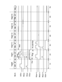
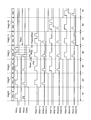
- FIG. 4 is a timing chart of a pixel included in the display device according to the embodiment of the present invention, and shows a time change of each signal shown in FIG.
- FIG. 4 also shows a timing chart of the pixel of n + 1 rows and m columns, but the basic operation is the same as that of the pixels of n rows and m columns.
- the activation state of each transistor is described in association with the high level. However, whether the high level or the low level is referred to as the activation state is arbitrary for each signal.
- an activated state or an activated state means a state where a source and a drain of a transistor are conductive, a state where a current flows between the source and the drain, and a state where a transistor is on.
- an inactivated state or an inactivated state means a state where a source and a drain of a transistor are non-conductive, a state where no current flows between the source and the drain, and a state where a transistor is off.
- the n rows and m columns of pixels include three operations within one horizontal period (horizontal scanning period). These are, in order, a reset operation, a threshold correction (threshold voltage variation correction) operation, a current correction (mobility variation correction), and a write operation. After these operations, the light emitting element OLED emits light over a plurality of horizontal periods following the one horizontal period.
- the periods corresponding to these operations are referred to as a reset period Prst, a threshold correction period Pcom, a current correction and writing period Pccom + Pwrt, and a light emission period Pemi, respectively.
- Each horizontal period is indicated by 1H, 2H, 3H, 4H, 5H, 6H, and 7H.
- a low level is supplied from the light emission control signal line BG (n) to the gate of the light emission control transistor BCT in the n rows and m columns, and the light emission control in the n + 1 rows and m columns from the light emission control signal line BG (n + 1).
- a low level is supplied to the gate of the transistor BCT, and both the light emission control transistors BCT in the nth row and mth column and the n + 1th row and mth column are turned off.
- the pixels in n rows and m columns and the pixels in n + 1 rows and m columns are in a dark state.
- the signal supplied from the scanning signal line SG (n) to the gate of the selection transistor SST in the n rows and m columns is changed from the low level to the high level, and the selection transistors SST in the n rows and m columns are turned on, as shown in FIG. Vini is written to node A (n).
- the signal supplied from the control line RG (n) to the gate of the initialization transistor RST in the n row and m column is changed from the low level to the high level, and the initialization transistor RST in the n row and m column is turned on, as shown in FIG. Vrst is written to the node B (n).
- the signal supplied from the capacitance control signal line EG (n) to the gate of the capacitance control transistor ECT of n rows and m columns is at a high level, and the capacitance control transistor ECT of n rows and m columns is on.
- Node B (n) and node B (n + 1) shown in FIG. 3 are brought into conduction, and Vrst is written to the node B (n + 1).
- the signal supplied from the scanning signal line SG (n + 1) to the gate of the selection transistor SST in the n + 1 row and m column is changed from the low level to the high level, and the selection transistor SST in the n + 1 row and m column is turned on.
- the initialization transistor RST of n + 1 rows and m columns may be on or off. That is, the signal on the control line RG (n + 1) may be at a high level or a low level. Further, writing Vini to the node A (n), writing Vini to the node A (n + 1), and writing Vrst to the node B (n) may be performed simultaneously.
- the potentials of the node A (n) in the nth row and mth column and the node A (n + 1) in the n + 1th row and mth column are set to Vini
- the node B (n) in the nth row and mth column is set to the n + 1th row m.
- the potential of node B (n + 1) in the column is set to Vrst. That is, the potential between the first terminal and the second terminal of the capacitor element in n rows and m columns is the same as the potential between the first terminal and the second terminal of each capacitor element in n + 1 rows and m columns. To. That is, it is possible to initialize the potential between the gate and the second terminal of the driving transistor DRT of n rows and m columns and the potential between the gate and the second terminal of the driving transistor DRT of n + 1 rows and m columns.
- the threshold correction operation will be described.
- the signal supplied from the control line RG (n) to the gate of the initialization transistor RST in n rows and m columns is changed from the high level to the low level, and the initialization transistor RST is turned off.
- Both the selection transistor SST of n rows and m columns and the selection transistor SST of n + 1 rows and m columns are kept on, and the potentials of the nodes A (n) and A (n + 1) are kept at Vini.
- the capacitance control transistor ECT of n rows and m columns maintains the on state, and the potentials of the node B (n) and the node B (n + 1) are maintained at Vrst.
- the signal supplied from the light emission control signal line BG (n) to the gate of the light emission control transistor BCT in the n rows and m columns is changed from the low level to the high level, and the light emission control transistors BCT in the n rows and m columns are turned on.
- VDD_H is supplied from the high potential power supply wiring PVDD to the drive transistor DRT of n rows and m columns via the light emission control transistor BCT.
- a current flows through the driving transistor DRT of n rows and m columns, and the potential of the node B (n) is shifted from Vrst to the high potential side.
- the threshold voltage Vthn of the driving transistor DRT of n rows and m columns can be held between the terminals.
- a write operation to be described later is performed from the state in which the threshold voltage Vthn is held in the capacitor element Cs. Therefore, even if there is a variation in the threshold voltage of each of the drive transistors DRT included in each of the plurality of pixels 108, the variation in the threshold voltage is removed when the light emitting element OLED included in each of the plurality of pixels 108 emits light. Can do.
- a signal supplied from the scanning signal line SG (n) to the gate of the selection transistor SST in the n rows and m columns is changed from the high level to the low level, and the selection transistors SST in the n rows and m columns are turned off. Further, the signal supplied from the scanning signal line SG (n + 1) to the gate of the selection transistor SST in the n + 1 row and m column is also changed from the high level to the low level, and the selection transistor SST in the n + 1 row and m column is also turned off.
- the capacitance control transistor ECT of n rows and m columns maintains the on state. At this time, the potentials of the node B (n) and the node B (n + 1) are kept at Vini ⁇ Vthn.
- the light emission control transistor BCT in the n rows and m columns maintains the on state.
- the initialization transistor RST is kept off.
- the capacitance control transistor ECT in n rows and m columns maintains the on state.
- the potentials of the nodes B (n) and B (n + 1) are kept at Vini ⁇ Vthn.
- the light emission control transistor BCT in the n rows and m columns maintains the on state.
- the initialization transistor RST is kept off.
- the signal supplied from the scanning signal line SG (n) to the gate of the selection transistor SST in the n rows and m columns is changed from the low level to the high level, and the selection transistors SST in the n rows and m columns are turned on.
- Vsig (m) is supplied from the video signal line SL (m) electrically connected to the first terminal of the selection transistor SST, and the potential of the node A (n) is changed from Vini to Vsig (m). That is, Vsig (m) is written to the node A (n). Since the gate voltage of the driving transistor DRT of n rows and m columns is also Vsig (m), the driving transistor DRT is turned on, and a current flows through the driving transistor DRT. Note that the input terminal of the light emitting element OLED of n rows and m columns and n + 1 rows and m columns and the first terminal of the additional capacitor Cel of n rows and m columns and n + 1 rows and m columns are electrically connected to the node B (n). ing.
- the potential of the node B (n) that is, the potential of the input terminal of the light emitting element OLED (here, the anode voltage of the light emitting element OLED) is the light emitting element. It is smaller than the threshold voltage of the OLED, and no current flows to the light emitting element OLED. Alternatively, the light emitting element OLED does not emit light.
- the voltage of the second terminal of the driving transistor DRT of n rows and m columns that is, the potential of the node B (n) increases.
- the potential increase of the node B (n) here also increases.
- the increased potentials of the nodes B (n) and B (n + 1) are expressed by the following formula (1) due to capacitive coupling via the capacitive element Cs included in the pixel of n rows and m columns.
- a (n) represents the potential of the node A (n)
- B (n) represents the potential of the node B (n).
- the potential difference (gate-source voltage) between the gate and the second terminal of the driving transistor DRT of n rows and m columns, that is, the potential difference between the node A (n) and the node B (n) is expressed by the following equation (2 ).
- the capacitor Cs of n rows and m columns holds the voltage shown in the equation (2).
- the current Id flowing from the first terminal to the second terminal of the driving transistor DRT of n rows and m columns is expressed by the following equation (3).
- ⁇ is a gain coefficient of the driving transistor DRT of n rows and m columns.
- the video signal can be written and the current of the driving transistor DRT can be corrected.
- the input terminal of the light emitting element OLED of n rows and m columns and n + 1 rows and m columns and the first terminal of the additional capacitor Cel of n rows and m columns and n + 1 rows and m columns are electrically connected by the capacitance control transistor ECT.
- the additional capacitor Cel in the (n + 1) rows and m columns can also contribute.
- the additional capacitance of the adjacent pixel here, the additional capacitance Cel of the pixel 108 in the n + 1 row and m column can be shared.
- the embodiment shows the potential difference between the node A (n) and the node B (n) as shown in Expression (2). That is, the gate-source voltage of the drive transistor DRT can be increased, and a high dynamic range can be realized.
- the light emission control transistor BCT in n rows and m columns maintains the on state.
- the initialization transistor RST is kept off.
- a signal supplied from the capacitance control signal line EG (n) to the gate of the capacitance control transistor ECT of n rows and m columns is changed from a high level to a low level, and the capacitance control transistor ECT of the n rows and m columns is turned off.
- the node B (n) and the node B (n + 1) are separated by turning off the capacitance control transistor ECT.
- a signal supplied from the scanning signal line SG (n) to the gate of the selection transistor SST in the n rows and m columns is changed from the high level to the low level, and the selection transistors SST in the n rows and m columns are turned off.
- the driving transistor DRT of n rows and m columns supplies current to the light emitting element OLED based on the voltage held in the capacitive element Cs. Therefore, light emission of the light emitting element OLED of n rows and m columns is started.
- the light emission current at this time is expressed by Equation (4).
- the light emission current is small because the capacitance value is only for the additional capacitance Cel of n rows and m columns.
- the first terminal of the additional capacitor Cel of n rows and m columns and n + 1 rows and m columns is electrically connected by the capacitance control transistor ECT, so that the additional capacitor Cel of n + 1 rows and m columns is shared. ing. Therefore, compared to the conventional case, when a video signal is input to the pixel 108 in the n row and m column, the capacity used by the pixel 108 is larger because the additional capacitor Cel included in the pixel 108 in the n + 1 row and m column is shared. Become.
- the fractional part of the expressions (2) and (4) becomes Cel / Cs + Cel when there is no capacitance control transistor ECT, but in the present invention, as shown in the expressions (2) and (4). 2Cel / Cs + 2Cel. Therefore, the maximum value of the light emission current that can flow to the light emitting element OLED can be increased.
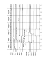
- FIG. 5 is a timing chart of pixels included in the display device according to the embodiment of the present invention.
- the timing chart of n + 2 rows and m columns and n + 3 rows and m columns is added to the timing chart of FIG.
- Each horizontal period is indicated by 1H, 2H, 3H, 4H, 5H, 6H, and 7H.
- the operations of the reset period Prst, the threshold correction period Pcom, the current correction and writing period Pccom + Pwrt, and the light emission period Pemi described above are sequentially repeated from the nth row mth column to the n + 3th row mth column shown in FIG.
- the current of the light emitting element included in the display device can be increased, and a high dynamic range can be realized.
- FIG. 6 is a schematic diagram showing the state of the pixels included in the display device according to the embodiment of the present invention for each horizontal period.
- FIG. 6 shows the operation state in each horizontal period shown in the timing chart of FIG. 5 from n rows to m columns to n + 3 rows and m columns, followed by n + 4 rows to m columns to n + 6 rows and m columns.
- Each horizontal period is indicated by 1H, 2H, 3H, 4H, 5H, and 6H.
- periods Prst to Pwrt indicate periods during which the above-described reset period Prst, threshold correction period Pcom, current correction and write period Pccom + Pwrt are performed.
- the capacitance control transistor ECT in the previous row electrically connects the capacitance Cs and the additional capacitance Cel included in the pixel in the previous row to the additional capacitance Cel included in the own pixel. It shows the period of the status. In other words, the state in which the adjacent pixels share the capacitance is shown.
- the additional capacitance Cel of the pixel in the (n + 2) th row and the mth column is electrically connected to the capacitance element Cs and the additional capacitance Cel included in the pixel in the (n + 1) th row and the mth column.
- one pixel has a period Cshr, a reset period Prst, and a threshold correction period in which the additional capacitor Cel included in the pixel is electrically connected to the capacitor Cs included in the pixel in the previous row and the additional capacitor Cel.
- Pcom current correction and writing period Pccom + Pwrt, and light emission period Pemi
- the horizontal period before the period Cshr may be the light emission period Pemi in the previous frame period.
- the capacitance control transistor ECT is provided, and the input terminal of the n-row m-column light emitting element OLED and the first terminal of the additional capacitor Cel, and the input terminal of the n + 1 row m-column light-emitting element OLED and the additional capacitor Cel of A large capacity can be secured by being electrically connected to the first terminal. Therefore, the current of the light emitting element can be increased and a high dynamic range can be realized.
- the capacitance (capacitance element Cs and additional capacitance Cel) included in the pixel is also reduced. Accordingly, the voltage held by the capacitor is reduced, and the maximum value of the current that can be passed to the light emitting element is also reduced.
- the capacitive element Cs and the additional capacitor Cel included in the pixel 108 in the n row and m column and the additional capacitor Cel included in the pixel 108 in the n + 1 row and m column are shared, so that the current flows to the light emitting element OLED. It is possible to prevent the maximum value of the possible current from becoming small. That is, it is possible to flow a sufficient amount of current to the light emitting element OLED.
- the display device can display with high gradation. Therefore, the display device and the driving method described above can provide a high-definition display device with high display quality.
- the pixel circuit in the second embodiment is the same as the pixel circuit shown in the pixel circuit diagram 300 of FIG.
- the capacitance control transistor ECT included in the pixel 108 in n rows and m columns and the capacitance control transistor ECT included in the pixel 108 in n + 1 rows and m columns are simultaneously turned on, so that n + 3 to n + 3
- a description will be given of sharing the additional capacitor Cel included in the pixel 108 in the row m column, securing a larger light emission current, and realizing a higher dynamic range.
- description may be abbreviate
- FIG. 7 is a timing chart of the pixels 108 from n rows and m columns to n + 3 rows and m columns included in the display device according to the embodiment of the present invention. Each horizontal period is indicated by 1H, 2H, 3H, 4H, 5H, 6H, and 7H.
- a high level signal is supplied from the capacitance control signal line EG (n) to the gate of the capacitance control transistor ECT in the nth row and mth column, and the capacitance control transistor ECT in the nth row and mth column is turned on.
- a high level signal is supplied from the capacitance control signal line EG (n + 1) to the gate of the capacitance control transistor ECT in the (n + 1) th row and the mth column, and the capacitance control transistor ECT in the (n + 1) th row and the mth column is turned on.
- a high level signal is supplied from the capacitance control signal line EG (n + 2) to the gate of the capacitance control transistor ECT of n + 2 rows and m columns, and the capacitance control transistor ECT of n + 2 rows and m columns is turned on.
- a high level signal is supplied from the capacitance control signal line EG (n + 3) to the gate of the capacitance control transistor ECT of n + 3 rows and m columns, and the capacitance control transistor ECT of n + 3 rows and m columns is turned on.
- the first terminal of the additional capacitor Cel in the row m column and the first terminal of the additional capacitor Cel in the (n + 3) row m column are electrically connected. Therefore, the potential difference (gate-source voltage) between the gate and the second terminal of the driving transistor DRT of n rows and m columns, that is, the potential difference between the node A (n) and the node B (n) is expressed by the following equation (5). It is represented by
- the current Id flowing from the first terminal to the second terminal of the driving transistor DRT of n rows and m columns is expressed by the following equation (6).
- ⁇ is a gain coefficient of the driving transistor DRT of n rows and m columns.
- the current Id flowing from the first terminal to the second terminal of the drive transistor DRT does not depend on the threshold value of the drive transistor DRT.
- the video signal can be written and the current of the driving transistor DRT can be corrected.
- the capacitance control transistor ECT electrically connects the input terminal of the light emitting element OLED from n rows to m columns to n + 3 rows and m columns and the first terminal of the additional capacitor Cel from n rows to m columns to n + 3 rows and m columns.
- the additional capacitor Cel included in the pixels 108 in the n + 1 rows and m columns to the n + 3 rows and m columns can be shared.
- the gate-source voltage of the drive transistor DRT can be further increased as compared with the first embodiment, and a higher dynamic range can be realized.
- the light emission control transistor BCT in n rows and m columns maintains the on state.
- the initialization transistor RST is kept off.
- a signal supplied from the capacitance control signal line EG (n) to the gate of the capacitance control transistor ECT of n rows and m columns is changed from a high level to a low level, and the capacitance control transistor ECT of the n rows and m columns is turned off.
- the node B (n) and the node B (n + 1) to the node B (n + 3) are separated by turning off the capacitance control transistor ECT.
- a signal supplied from the scanning signal line SG (n) to the gate of the selection transistor SST in the n rows and m columns is changed from the high level to the low level, and the selection transistors SST in the n rows and m columns are turned off.
- the driving transistor DRT of n rows and m columns supplies current to the light emitting element OLED based on the voltage held in the capacitive element Cs. Accordingly, the light emitting elements of n rows and m columns start to emit light.
- the light emission current at this time is expressed by Expression (6).
- the light emission current is small because the capacitance value is only for the additional capacitance Cel of n rows and m columns.
- the capacity used by the pixel 108 is the additional capacitor Cel included in the pixel 108 in the n + 1 row m column to the n + 3 row m column. It grows as much as you share. Therefore, the maximum value of the light emission current that can flow to the light emitting element OLED can be increased.
- FIG. 8 is a schematic diagram showing the state of the pixels included in the display device according to the embodiment of the present invention for each horizontal period.
- Each horizontal period is indicated by 1H, 2H, 3H, 4H, 5H, and 6H.
- periods Prst to Pwrt indicate periods during which the above-described reset period Prst, threshold correction period Pcom, current correction and write period Pccom + Pwrt are performed.
- a period Cshr in the figure shows a state in which the additional capacitor Cel is shared by adjacent pixels, for example, the pixels 108 in the n-th row and m-th column to the (n + 3) -th row and m-column by the capacitance control transistor ECT.
- the pixel in the (n + 2) th row and the mth column is in a state in which a reset operation, a threshold correction operation, a current correction, and a write operation are performed in the period H3.
- the additional capacitor Cel included in each pixel is electrically connected by the capacitance control transistor ECT included in the four pixels of n rows and m columns, n + 1 rows and m columns, n + 2 rows and m columns, and n + 3 rows and m columns.
- the additional capacitor Cel included in each pixel is electrically connected by the capacitance control transistor ECT included in the three pixels of n rows and m columns, n + 1 rows and m columns, and n + 2 rows and m columns. Also good.
- the capacitance control transistor ECT is provided, and the input terminal of the light emitting element OLED from n rows to m columns to n + 3 rows and m columns and the first terminal of the additional capacitor Cel from n rows to m columns to n + 3 rows and m columns are electrically connected.
- the larger capacity can be ensured by connecting them in the same manner. Therefore, the current of the light emitting element can be further increased and a higher dynamic range can be realized. Therefore, even in a display device having a small pixel size, a large current for the light emitting element to emit light can be supplied, and a reduction in luminance of the display device can be suppressed.
- the display device can realize high gradation display. Therefore, the display device and the driving method described above can provide a high-definition display device with high display quality.
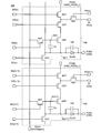
- the present embodiment further includes an initialization signal input transistor IST.
- description may be abbreviate
- FIG. 9 is a pixel circuit diagram 400 provided in the pixel 108 included in the display device according to the embodiment of the present invention.
- the pixel circuit diagram 400 shows two pixels 108 arranged in the display area 106 in n rows and m columns and n + 1 rows and m columns.
- the pixel 108 has a configuration in which the pixel circuit diagram 300 shown in FIG. 3 further includes an initialization signal input transistor IST.
- each transistor has a gate and a pair of terminals (first terminal and second terminal), and the capacitor Cs has a pair of terminals (first terminal and second terminal).
- the additional capacitor Cel has a pair of terminals (a first terminal and a second terminal).
- capacitance Cel it may be a parasitic capacity
- the configuration changed from FIG. 3 will be described. Since the configuration other than the change is the same as that of FIG. 3, the description thereof is omitted here.
- the gate of the initialization signal input transistor IST is electrically connected to the initialization signal control line IG (n), the first terminal is electrically connected to the initialization signal line SL2 (m), and the second terminal Are electrically connected to the gate of the drive transistor DRT, the second terminal of the selection transistor SST, and the first terminal of the capacitor Cs.
- the potential Vini of the initialization signal is input from the video signal line SL (m) to the pixel 108 (to the selection transistor SST).
- Vini is input from the initialization signal line SL2 (m) to the initialization signal input transistor IST.
- the pixel of n rows and m columns among the pixels 108 included in the pixel circuit has been described.
- the configuration of the pixel in the n + 1 row and the m column is the same as that of the pixel in the n row and the m column.
- FIG. 10 is a timing chart of a pixel included in the display device according to the embodiment of the present invention, and shows a time change of each signal shown in FIG.
- FIG. 10 also shows a timing chart of pixels of n + 1 rows and m columns, but the basic operation is the same as that of pixels of n rows and m columns.
- the reset operation, the threshold value, and the reset period Prst, the threshold value correction period Pcom, the current correction and writing period Pccom + Pwrt, and the light emission period Pemi are performed, respectively.
- the initialization signal input transistor IST Prior to the reset operation, the initialization signal input transistor IST is turned on by supplying a high level from the initialization signal line IG (n) to the gate of the initialization signal input transistor IST in n rows and m columns, as shown in FIG.
- An operation of writing Vrst to the node B (n) may be performed. Both of these two operations may be performed, or any one of these two operations may be performed.
- Vini in 1H and Vsig (d) in 1H may be the same.
- a low level is supplied from the light emission control signal line BG (n) to the gate of the light emission control transistor BCT in the n rows and m columns, and the light emission control in the n + 1 rows and m columns from the light emission control signal line BG (n + 1).
- a low level is supplied to the gate of the transistor BCT, and both transistors are turned off. At this time, the pixels in n rows and m columns and the pixels in n + 1 rows and m columns are in a dark state.
- a high level signal is supplied from the initialization signal control line IG (n) to the gate of the initialization signal input transistor IST in the nth row and mth column, and the initialization signal input transistor IST in the nth row and mth column is turned on. Further, a high level signal is supplied from the initialization signal control line IG (n + 1) to the gate of the initialization signal input transistor IST in the (n + 1) th row and the mth column, and the initialization signal input transistor IST in the (n + 1) th row and the mth column is turned on. As a result, Vini is written to the nodes A (n) and A (n + 1) shown in FIG.
- a low level signal is supplied from the scanning signal line SG (n) to the gate of the selection transistor SST of n rows and m columns, and the selection transistor SST of the n rows and m columns is off.
- a low level signal is supplied from the scanning signal line SG (n + 1) to the gates of the selection transistors SST in the (n + 1) rows and m columns, and the selection transistors SST in the (n + 1) rows and m columns are inactivated. Is off.
- the signal supplied from the control line RG (n) to the gate of the initialization transistor RST in the n rows and m columns is changed from the low level to the high level, so that the initialization transistor RST in the n rows and m columns is turned on. Vrst is written in (n).
- the signal supplied from the capacitance control signal line EG (n) to the gate of the capacitance control transistor ECT of n rows and m columns is changed from the low level to the high level, and the capacitance control transistor ECT of the n rows and m columns is turned on.
- Vrst is written to the node B (n + 1) shown in FIG.
- the initialization transistor RST of n + 1 rows and m columns may be on or off. Further, writing Vini to the node A (n), writing Vini to the node A (n + 1), and writing Vrst to the node B (n) may be performed simultaneously.
- the operation of setting the potential of the node A (n) in the nth row and mth column and the node A (n + 1) in the n + 1th row and mth column to Vini which is performed by the selection transistor SST.
- the initialization signal input transistor IST takes charge.
- the selection transistor SST is responsible for the operation of writing the video signal to the gate of the drive transistor DRT, and the initialization signal input transistor IST is responsible for the above-described operation, so that the time for the write operation and the time for the initialization signal input operation are sufficient. Can be secured, and the driving of the pixel can be stabilized.
- the threshold correction operation will be described. Subsequent to the reset operation, the signal supplied from the control line RG (n) to the gate of the initialization transistor RST in n rows and m columns is changed from the high level to the low level, and the initialization transistor RST is turned off. Both the n-row and m-column selection transistor SST and the (n + 1) row and m-column selection transistor SST maintain the OFF state. Both the initialization signal input transistors IST of the n-th row and the m-th column and the (n + 1) -th row and the m-th column maintain the on state. The potentials of the nodes A (n) and A (n + 1) are kept at Vini.
- the capacitance control transistor ECT of n rows and m columns maintains the on state, and the potentials of the node B (n) and the node B (n + 1) are maintained at Vrst.
- a high level signal is supplied from the light emission control signal line BG (n) to the gate of the light emission control transistor BCT in the n rows and m columns, and the light emission control transistors BCT in the n rows and m columns are turned on.
- VDD_H is supplied from the high potential power supply wiring PVDD to the drive transistor DRT of n rows and m columns via the light emission control transistor BCT.
- the threshold correction period Pcom the first terminal and the second terminal of the capacitor element Cs in the n + 1 row and m column, the first terminal and the second terminal of the capacitor element Cs in the n row and m column, and the second terminal.
- the threshold voltage Vthn of the driving transistor DRT of n rows and m columns can be held between the terminals. Therefore, the threshold value of the drive transistor DRT can be corrected as described in the first embodiment.
- Both the n-row and m-column selection transistor SST and the (n + 1) row and m-column selection transistor SST maintain the OFF state.
- the initialization signal input transistor IST of (n + 1) rows and m columns is kept on.
- the signal supplied from the initialization signal control line IG (n) to the gate of the initialization signal input transistor IST of n rows and m columns is changed from the high level to the low level, and the initialization signal input transistor IST of the n rows and m columns is turned off. .
- the light emission control transistor BCT in the n rows and m columns maintains the on state.
- the initialization transistor RST is kept off.
- the initialization signal input transistor IST in the (n + 1) th row and the mth column is kept on.
- the initialization signal input transistor IST of n rows and m columns maintains an off state.
- the other driving methods are the same as those in FIG. Since the initialization signal input transistor IST in the (n + 1) row and the m column is maintained in the on state, the capacitor element Cs included in the pixel 108 in the (n + 1) row and the m column in the writing period Pwrt for writing the video signal to the pixel 108 in the n row and the m column. An initialization signal is input to the first terminal.
- the capacitor element Cs in the (n + 1) row and m column includes the n row and m column additional capacitor Cel and It can be shared with the capacitive element Cs.
- the potentials of the nodes B (n) and B (n + 1) are expressed by the following formula (7). Further, the potential difference (gate-source voltage) between the gate and the second terminal of the driving transistor DRT of n rows and m columns, that is, the potential difference between the node A (n) and the node B (n) is expressed by the following equation (8). expressed.
- the current Id flowing from the first terminal to the second terminal of the driving transistor DRT of n rows and m columns is expressed by the following equation (9) and does not depend on the threshold value of the driving transistor DRT.
- the mobility ⁇ of each of the drive transistors DRT included in each of the plurality of pixels 108 varies, the light emitting element OLED included in each of the plurality of pixels 108 is When light is emitted, variation in mobility ⁇ can be removed.
- the video signal can be written and the current of the driving transistor DRT can be corrected.
- the light emission control transistor BCT in n rows and m columns maintains the on state.
- the initialization transistor RST is kept off.
- the initialization signal input transistor IST of (n + 1) rows and m columns is kept on.
- the initialization signal input transistor IST of n rows and m columns maintains an off state.
- a signal supplied from the capacitance control signal line EG (n) to the gate of the capacitance control transistor ECT of n rows and m columns is changed from a high level to a low level, and the capacitance control transistor ECT of the n rows and m columns is turned off.
- the node B (n) and the node B (n + 1) are separated by turning off the capacitance control transistor ECT.
- a signal supplied from the scanning signal line SG (n) to the gate of the selection transistor SST in the n rows and m columns is changed from the high level to the low level, and the selection transistors SST in the n rows and m columns are turned off.
- the driving transistor DRT of n rows and m columns supplies current to the light emitting element OLED based on the voltage held in the capacitive element Cs. Therefore, light emission of the light emitting element OLED of n rows and m columns is started.
- the light emission current at this time is expressed by the equation (4) shown above.
- the initialization signal input transistor IST performs initialization in the reset operation, and the selection transistor SST performs writing. Since the initialization signal input transistor IST and the selection transistor SST can be controlled independently of each other, the write operation and the initialization operation can be clarified. Therefore, a sufficient time for the write operation and a time for the initialization signal input operation can be ensured, and the pixel drive can be stabilized. Further, by providing the capacitance control transistor ECT, the current of the light emitting element can be increased and a high dynamic range can be realized. Since the initialization is clearly performed, the threshold correction and current correction of the driving transistor can be performed with high accuracy. Therefore, the display device and the driving method described above can provide a high-definition display device with high display quality.
- FIG. 11 is a pixel circuit diagram 500 included in the display device according to the embodiment of the present invention.
- the pixel circuit diagram 500 shows two pixels 108 arranged in the display area 106 in n rows and m columns and n + 1 rows and m columns.
- the pixel circuit diagram 500 is different from the pixel circuit diagram 300 shown in FIG. 3 in that the position where the initialization transistor RST is electrically connected is changed and further includes a current correction transistor CCT. Shows the configuration. As in the description of FIG. 3, each transistor has a gate and a pair of terminals (first terminal and second terminal), and the capacitor Cs has a pair of terminals (first terminal and second terminal). And the additional capacitor Cel has a pair of terminals (a first terminal and a second terminal).
- capacitance Cel it may be a parasitic capacity
- the gate of the selection transistor SST is electrically connected to the scanning signal line SG (n), the first terminal is electrically connected to the video signal line SL (m), and the second terminal is the gate of the driving transistor DRT.
- the first terminal of the drive transistor DRT is electrically connected to the second terminal of the current correction transistor CCT, and the second terminal is electrically connected to the input terminal of the light emitting element OLED and the second terminal of the capacitor element Cs.
- the gate of the current correction transistor CCT is electrically connected to the current correction signal line CG (n), and the first terminal is electrically connected to the second terminal of the light emission control transistor BCT and the second terminal of the initialization transistor RST. Connected to.
- the gate of the light emission control transistor BCT is electrically connected to the light emission control signal line BG (n), and the first terminal is electrically connected to the high potential power supply wiring PVDD.
- the first terminal of the initialization transistor RST is electrically connected to the bias line VL, and the gate is electrically connected to the control line RG (n).
- the first terminal of the additional capacitor Cel is electrically connected to the second terminal of the drive transistor DRT, and the second terminal of the additional capacitor Cel is electrically connected to the low potential power supply line PVSS.
- the output terminal (or common electrode) of the light emitting element OLED is electrically connected to the low potential power wiring PVSS.
- the fixed potential VSS applied to the low potential power supply wiring PVSS may be a fixed potential lower than the low potential VDD_L, and may be a ground potential, for example.
- the gate of the capacitance control transistor ECT is electrically connected to the capacitance control signal line EG (n), the first terminal is the second terminal of the capacitance element Cs, the input terminal of the light emitting element OLED, and the first of the additional capacitance Cel. And the second terminal of the driving transistor DRT.
- the second terminals of the capacitance control transistors ECT are the first terminals of the (n + 1) th row capacitance control transistors ECT, the second terminals of the (n + 1) th row capacitance elements Cs, the input terminals of the (n + 1) th row light emitting elements OLED, and the (n + 1) th row.
- the pixel of n rows and m columns among the two pixels 108 illustrated in FIG. 11 has been described.
- the configuration of the pixel in the n + 1 row and the m column is the same as that of the pixel in the n row and the m column.
- FIG. 12 is a timing chart of a pixel included in the display device according to the embodiment of the present invention, and shows a time change of each signal shown in FIG.
- FIG. 12 also shows a timing chart of pixels of n + 1 rows and m columns, but the basic operation is the same as that of pixels of n rows and m columns.
- the reset operation, the threshold value, and the reset period Prst, the threshold value correction period Pcom, the current correction and writing period Pccom + Pwrt, and the light emission period Pemi are performed, respectively.
- a high level is supplied from the scanning signal line SG (n) to the gates of the selection transistors SST in the n rows and m columns, and the operation of writing Vini to the node A (n) shown in FIG. Also good.
- a high level is supplied from the light emission control signal line BG (n) to the gate of the light emission control transistor BCT of n rows and m columns, and a high level is supplied from the light emission control signal line BG (n + 1) to the gate of the light emission control transistor BCT of n + 1 rows and m columns.
- both transistors may be turned on. Both of these two operations may be performed, or any one of these two operations may be performed.
- Vini in 1H and Vsig (d) in 1H may be the same.
- the signal supplied from the current correction signal line CG (n) to the gate of the current correction transistor CCT in the n rows and m columns is changed from the low level to the high level, and the current correction transistors CCT in the n rows and m columns are turned on. become.
- a low level is supplied from the light emission control signal line BG (n) to the gate of the light emission control transistor BCT in the n row and m column, and the gate of the light emission control transistor BCT in the n + 1 row and m column from the light emission control signal line BG (n + 1). Is supplied with a low level, and both transistors are turned off.
- the pixels in n rows and m columns and the pixels in n + 1 rows and m columns are in a dark state.
- the signal supplied from the scanning signal line SG (n) to the gate of the selection transistor SST in the n rows and m columns is changed from the low level to the high level, and the selection transistors SST in the n rows and m columns are turned on, as shown in FIG. Vini is written to node A (n).
- the signal supplied from the control line RG (n) to the gate of the initialization transistor RST in the n row and m column is changed from the low level to the high level, and the initialization transistor RST in the n row and m column is turned on, as shown in FIG.
- Vrst is written to the node B (n) via the current correction transistor CCT.
- the signal supplied from the capacitance control signal line EG (n) to the gate of the capacitance control transistor ECT of n rows and m columns is changed from the low level to the high level, and the capacitance control transistor ECT of the n rows and m columns is turned on.
- Node B (n) and node B (n + 1) shown in FIG. 11 become conductive, and Vrst is written to node B (n + 1).
- the signal supplied from the scanning signal line SG (n + 1) to the gate of the selection transistor SST in the n + 1 row and m column is changed from the low level to the high level, and the selection transistor SST in the n + 1 row and m column is turned on. Vini is written in At this time, the initialization transistor RST of n + 1 rows and m columns may be on or off. Further, writing Vini to the node A (n), writing Vini to the node A (n + 1), and writing Vrst to the node B (n) may be performed simultaneously.
- the potentials of the node A (n) in the nth row and mth column and the node A (n + 1) in the n + 1th row and mth column are set to Vini
- the node B (n) in the nth row and mth column is set to the n + 1th row m.
- the potential of node B (n + 1) in the column is set to Vrst. That is, the potential between the first terminal and the second terminal of the capacitor element in n rows and m columns is the same as the potential between the first terminal and the second terminal of each capacitor element in n + 1 rows and m columns. To. That is, it is possible to initialize the potential between the gate and the second terminal of the driving transistor DRT of n rows and m columns and the potential between the gate and the second terminal of the driving transistor DRT of n + 1 rows and m columns.
- the threshold correction operation will be described.
- the signal supplied from the control line RG (n) to the gate of the initialization transistor RST in n rows and m columns is changed from the high level to the low level, and the initialization transistor RST is turned off.
- Both the selection transistor SST of n rows and m columns and the selection transistor SST of n + 1 rows and m columns are kept on, and the potentials of the nodes A (n) and A (n + 1) are kept at Vini.
- the capacitance control transistor ECT of n rows and m columns maintains the on state, and the potentials of the node B (n) and the node B (n + 1) are maintained at Vrst.
- the current correcting transistor CCT in the n rows and the m columns maintains the on state.
- a high level is supplied from the light emission control signal line BG (n) to the gate of the light emission control transistor BCT in the n rows and m columns, and the light emission control transistors BCT in the n rows and m columns are turned on.
- VDD_H is supplied from the high potential power supply wiring PVDD to the drive transistor DRT of n rows and m columns via the light emission control transistor BCT.
- a current flows through the driving transistor DRT of n rows and m columns, and the potential of the node B (n) is shifted from Vrst to the high potential side.
- the threshold correction period Pcom the first terminal and the second terminal of the capacitor element Cs in the n + 1 row and m column, the first terminal and the second terminal of the capacitor element Cs in the n row and m column, and the second terminal.
- the threshold voltage Vthn of the driving transistor DRT of n rows and m columns can be held between the terminals. Therefore, the threshold value of the drive transistor DRT can be corrected as described in the first embodiment.
- a signal supplied from the scanning signal line SG (n) to the gate of the selection transistor SST in the n rows and m columns is changed from the high level to the low level, and the selection transistors SST in the n rows and m columns are turned off. Further, the signal supplied from the scanning signal line SG (n + 1) to the gate of the selection transistor SST in the (n + 1) th row and the mth column is also changed from the high level to the low level, and the selection transistor SST in the (n + 1) th row / mth column is also turned off.
- the capacitance control transistor ECT of n rows and m columns maintains the on state.
- the potentials of the node B (n) and the node B (n + 1) are kept at Vini ⁇ Vthn.
- the light emission control transistor BCT in the n rows and m columns maintains the on state.
- the initialization transistor RST is kept off.
- the current correcting transistor CCT in the n rows and the m columns maintains the on state.
- the current correction transistor CCT in the nth row and the mth column maintains the on state.
- the other driving methods are the same as those in FIG. Similarly to FIG. 9, in the writing period Pwrt in which the video signal is written to the pixel 108 in the n row and m column, the initialization signal is input to the first terminal of the capacitor Cs included in the pixel 108 in the n + 1 row and m column. Yes. Therefore, when the video signal input to the pixel 108 in the n rows and m columns is held, the capacitor element Cs in the (n + 1) rows and m columns can be used.
- the potentials of the node B (n) and the node B (n + 1) are expressed by the equation (7) shown above. Further, the potential difference (gate-source voltage) between the gate and the second terminal of the driving transistor DRT of n rows and m columns, that is, the potential difference between the node A (n) and the node B (n) is expressed by the equation (8 ). Furthermore, the current Id flowing from the first terminal to the second terminal of the driving transistor DRT of n rows and m columns is expressed by the above-described equation (9) and does not depend on the threshold value of the driving transistor DRT.
- the video signal can be written and the current of the driving transistor DRT can be corrected.
- the operation during the light emission period Pemi will be described.
- the n-row m-column current correction transistor CCT is kept on.
- the other driving methods are the same as those in FIG.
- the node B (n) and the node B (n + 1) are separated by turning off the capacitance control transistor ECT. Thereafter, light emission of the light emitting element OLED of n rows and m columns is started.
- the light emission current at this time is expressed by the equation (4) shown above.
- the position where the initialization transistor RST is electrically connected is changed, and the current correction transistor CCT is added. .
- the current correction transistor CCT By adding the current correction transistor CCT, it is possible to select whether or not the potential or current from PVDD supplied from the light emission control transistor BCT is supplied to the drive transistor DRT. That is, the light emission control transistor BCT can be shared by subpixels adjacent to each other in a direction crossing one direction. For example, when one pixel is represented by three sub-pixels displaying R (red), G (green), and B (blue), each video signal is sent at the same timing, so that three sub-pixels Thus, one light emission control transistor BCT can be shared.
- FIG. 11 illustrates an example in which one light emission control transistor BCT is provided in one pixel.
- one light emission control transistor BCT may be shared by a plurality of adjacent pixels in the same row.
- one or more light emission control transistors BCT may be shared by the two or more pixels.
- one light emission control transistor BCT may be shared by six subpixels.
- the second terminal of the initialization transistor RST is connected between the light emission control transistor BCT and the current correction transistor CCT.
- the current correction transistor CCT can independently control whether to supply the potential or current from the light emission control transistor BCT to the drive transistor DRT and to perform threshold correction. Therefore, according to the present invention, light emission, threshold correction, and current correction can be performed with high accuracy.
- the initialization transistor RST can be shared by pixels adjacent in one direction, the number of transistors per pixel can be reduced, and the pixel layout can be reduced.
- FIG. 11 shows an example in which one initialization transistor RST is provided for one pixel. However, as described above, one initialization transistor RST may be provided for one column.
- the display device and the driving method described above can provide a high-definition display device with high display quality.
- FIG. 13 is a pixel circuit diagram 600 included in the display device according to the embodiment of the present invention.
- the pixel circuit diagram 600 shows two pixels 108 arranged in the display area 106 in n rows and m columns and n + 1 rows and m columns.
- a pixel circuit diagram 600 shows a configuration further including an initialization signal input transistor IST, as compared with the pixel circuit diagram 500 shown in FIG. Similarly to the description of FIG. 11, each transistor has a gate and a pair of terminals (first terminal and second terminal), and the capacitor Cs has a pair of terminals (first terminal and second terminal). And the additional capacitor Cel has a pair of terminals (a first terminal and a second terminal).
- capacitance Cel it may be a parasitic capacity
- the configuration changed from FIG. 11 will be described.
- the configuration other than the change is the same as in FIG.
- the gate of the initialization signal input transistor IST is electrically connected to the initialization signal control line SG (n)
- the first terminal is electrically connected to the initialization signal line SL2 (m)
- the second terminal Are electrically connected to the gate of the drive transistor DRT, the second terminal of the selection transistor SST, and the first terminal of the capacitor Cs.
- Vini is input from the initialization signal line SL2 (m) to the initialization signal input transistor IST.
- the pixel of n rows and m columns among the pixels 108 included in the pixel circuit has been described.
- the configuration of the pixel in the n + 1 row and the m column is the same as that of the pixel in the n row and the m column.
- FIG. 14 is a timing chart of a pixel included in the display device according to the embodiment of the present invention, and shows a time change of each signal shown in FIG.
- FIG. 14 also shows a timing chart of pixels of n + 1 rows and m columns, but the basic operation is the same as that of pixels of n rows and m columns.
- the reset operation, the threshold value, and the reset period Prst, the threshold value correction period Pcom, the current correction and writing period Pccom + Pwrt, and the light emission period Pemi are performed, respectively.
- a high level is supplied from the initialization signal control line IG (n) to the gate of the initialization signal input transistor IST in the n rows and the m columns to turn on the initialization signal input transistor IST, as shown in FIG.
- the operation of writing Vini to the node A (n) shown may be performed.
- a high level is supplied from the light emission control signal line BG (n) to the gate of the light emission control transistor BCT of n rows and m columns, and a high level is supplied from the light emission control signal line BG (n + 1) to the gate of the light emission control transistor BCT of n + 1 rows and m columns.
- both transistors may be turned on. Both of these two operations may be performed, or any one of these two operations may be performed.
- Vini in 1H and Vsig (d) in 1H may be the same.
- the signal supplied from the current correction signal line CG (n) to the gate of the current correction transistor CCT in the n rows and m columns is changed from the low level to the high level, and the current correction transistors CCT in the n rows and m columns are turned on. become.
- a low level signal is supplied from the scanning signal line SG (n) to the gate of the selection transistor SST in the n rows and the m columns, and the selection transistors SST in the n rows and the m columns are turned off.
- a low level signal is supplied from the scanning signal line SG (n + 1) to the gate of the selection transistor SST in the (n + 1) th row and the mth column, and the selection transistor SST in the (n + 1) th row and the mth column is turned off.
- a high level signal is supplied from the initialization signal control line IG (n) to the gate of the initialization signal input transistor IST in the nth row and the mth column, and the initialization signal input transistor IST in the nth row and the mth column is turned on. Vini is written to the node A (n) shown in FIG.
- a high level signal is supplied from the initialization signal control line IG (n + 1) to the gate of the initialization signal input transistor IST in the (n + 1) th row and the mth column, and the initialization signal input transistor IST in the (n + 1) th row and the mth column is turned on. Vini is written to A (n + 1).
- a low level is supplied from the light emission control signal line BG (n) to the gate of the light emission control transistor BCT in the n row and m column, and the gate of the light emission control transistor BCT in the n + 1 row and m column from the light emission control signal line BG (n + 1). Is supplied with a low level, and both transistors are turned off.
- the pixels in n rows and m columns and the pixels in n + 1 rows and m columns are in a dark state.
- the signal supplied from the control line RG (n) to the gate of the initialization transistor RST in the n row and m column is changed from the low level to the high level, and the initialization transistor RST in the n row and m column is turned on, as shown in FIG. Vrst is written to the node B (n).
- the signal supplied from the capacitance control signal line EG (n) to the gate of the capacitance control transistor ECT of n rows and m columns is changed from the low level to the high level, and the capacitance control transistor ECT of the n rows and m columns is turned on.
- Node B (n) and node B (n + 1) shown in FIG. 13 become conductive, and Vrst is written to node B (n + 1).
- the initialization transistor RST of n + 1 rows and m columns may be on or off. Further, writing Vini to the node A (n), writing Vini to the node A (n + 1), and writing Vrst to the node B (n) may be performed simultaneously.
- the potentials of the node A (n) in the nth row and mth column and the node A (n + 1) in the n + 1th row and mth column are set to Vini
- the node B (n) in the nth row and mth column is set to the n + 1th row m.
- the potential of node B (n + 1) in the column is set to Vrst. That is, the potential between the first terminal and the second terminal of the capacitor element in n rows and m columns is the same as the potential between the first terminal and the second terminal of each capacitor element in n + 1 rows and m columns. To. That is, it is possible to initialize the potential between the gate and the second terminal of the driving transistor DRT of n rows and m columns and the potential between the gate and the second terminal of the driving transistor DRT of n + 1 rows and m columns.
- the threshold correction operation will be described.
- the signal supplied from the control line RG (n) to the gate of the initialization transistor RST in n rows and m columns is changed from the high level to the low level, and the initialization transistor RST is turned off.
- Both the n-row and m-column selection transistor SST and the (n + 1) row and m-column selection transistor SST maintain the OFF state.
- Both the initialization signal input transistors IST in the n-th row and the m-th column and the (n + 1) -th row and the m-th column maintain the on state, and the potentials of the node A (n) and the node A (n + 1) are kept at Vini.
- the capacitance control transistor ECT of n rows and m columns maintains the on state, and the potentials of the node B (n) and the node B (n + 1) are maintained at Vrst.
- the current correcting transistor CCT in the n rows and the m columns maintains the on state.
- a high level is supplied from the light emission control signal line BG (n) to the gate of the light emission control transistor BCT in the n rows and m columns, and the light emission control transistors BCT in the n rows and m columns are turned on.
- VDD_H is supplied from the high potential power supply wiring PVDD to the drive transistor DRT of n rows and m columns via the light emission control transistor BCT.
- a current flows through the driving transistor DRT of n rows and m columns, and the potential of the node B (n) is shifted from Vrst to the high potential side.
- the threshold correction period Pcom the first terminal and the second terminal of the capacitor element Cs in the n + 1 row and m column, the first terminal and the second terminal of the capacitor element Cs in the n row and m column, and the second terminal.
- the threshold voltage Vthn of the driving transistor DRT of n rows and m columns can be held between the terminals. Therefore, the threshold value of the drive transistor DRT can be corrected as described in the first embodiment.
- Both the n-row and m-column selection transistor SST and the (n + 1) row and m-column selection transistor SST maintain the OFF state.
- the initialization signal input transistor IST of (n + 1) rows and m columns is kept on.
- the signal supplied from the initialization signal control line IG (n) to the gate of the initialization signal input transistor IST of n rows and m columns is changed from the high level to the low level, and the initialization signal input transistor IST of the n rows and m columns is turned off. .
- the light emission control transistor BCT in the n rows and m columns maintains the on state.
- the light emission control transistors BCT in the (n + 1) rows and m columns are kept on.
- the initialization transistor RST is kept off.
- the capacitance control transistor ECT of n rows and m columns maintains the on state.
- the potentials of the node B (n) and the node B (n + 1) are kept at Vini ⁇ Vthn.
- the current correcting transistor CCT in the n rows and the m columns maintains the on state.
- the potential difference (gate-source voltage) between the gate and the second terminal of the driving transistor DRT of n rows and m columns that is, the potential difference between the node A (n) and the node B (n) is expressed by the equation (2 ).
- the current Id flowing from the first terminal to the second terminal of the driving transistor DRT of n rows and m columns is expressed by the above-described equation (4) and does not depend on the threshold value of the driving transistor DRT.
- the video signal can be written and the current of the driving transistor DRT can be corrected.
- the operation during the light emission period Pemi will be described.
- the n-row m-column current correction transistor CCT is kept on.
- the initialization signal input transistor IST of (n + 1) rows and m columns is kept on.
- the initialization signal input transistor IST of n rows and m columns maintains an off state.
- the other driving method is the same as in FIG.
- the node B (n) and the node B (n + 1) are separated by turning off the capacitance control transistor ECT.
- light emission of the light emitting element OLED of n rows and m columns is started.
- the light emission current at this time is expressed by the equation (4) shown above.
- an initialization signal input transistor IST is added as compared with the pixel circuit diagram 500 shown in FIG. Since the initialization signal input transistor IST and the selection transistor SST can be controlled independently of each other, the write operation and the initialization operation can be clarified. Further, by providing the capacitance control transistor ECT, the maximum value of the light emission current that can flow can be increased, and a high dynamic range can be realized. According to the present invention, since the initialization is clearly performed, threshold correction and current correction of the driving transistor can be performed with high accuracy. Therefore, the display device and the driving method described above can provide a high-definition display device with high display quality.
- FIG. 13 shows an example in which one light emission control transistor BCT is provided in one pixel, but one light emission control transistor BCT may be shared by a plurality of adjacent pixels in the same row. For example, one light emission control transistor BCT may be shared by three adjacent subpixels in the same row.
- FIG. 13 shows an example in which one initialization transistor RST is provided for one pixel, but one initialization transistor RST may be provided for one column.
- the number of transistors per pixel can be reduced, and the pixel layout can be reduced.
- the storage capacitor and the additional capacitor can be increased, so that the maximum value of the light emission current that can be passed can be increased and the dynamic range can be widened. Therefore, a high-definition display device with high gradation and high luminance can be provided.
- FIG. 15 is a schematic cross-sectional view of the pixel 108 included in the display device 100. Specifically, FIG. 15 shows a schematic cross-sectional structure (film formation structure) of the capacitor Cs, the drive transistor DRT, the additional capacitor Cel, and the light emitting element OLED included in the pixel 108.
- the display device 100 has a driving transistor DRT and a capacitive element Cs on a first substrate 102 via a base film 140 having an arbitrary configuration.
- the base film 140 is formed of, for example, silicon nitride, silicon oxide, or a stack of silicon nitride and silicon oxide.
- the drive transistor DRT includes a semiconductor film 162, a gate insulating film 164, a gate electrode 166, and a source / drain electrode 168.
- a region overlapping with the gate electrode 166 in the semiconductor film 162 is a channel region, and the pair of source / drain regions are sandwiched between the channel regions.
- the source / drain electrode 168 is electrically connected to the source / drain region through an opening provided in the interlayer film 152 and the gate insulating film 164.
- the semiconductor film 162 extends to below the storage capacitor electrode 172.
- the capacitor element Cs is formed by a semiconductor film 162, a storage capacitor electrode 172, and a gate insulating film 164 sandwiched between them.
- the components forming the capacitive element Cs are not limited to the above.
- the capacitor element Cs may be formed by causing the storage capacitor electrode 172 and the pixel electrode of the light emitting element OLED to face each other with an insulating film interposed therebetween.
- a first planarizing film 158 that absorbs unevenness due to these and gives a flat surface is provided.
- An opening 190 reaching the source / drain electrode 168 is provided in the first planarization film 158. Through the opening 190, the source / drain electrode 168 and the pixel electrode (first electrode 182 described later) of the light emitting element OLED are electrically connected.
- An additional capacitance electrode 192 is provided on the first planarization film 158.
- a capacitor insulating film 194 is formed so as to cover the additional capacitor electrode 192 and the first planarization film 158.
- the additional capacitor electrode 192 forms the additional capacitor Cel together with the capacitor insulating film 194 and the first electrode 182 of the light emitting element OLED formed thereon, and contributes to the reduction of the variation in light emission of the light emitting element OLED.
- the components that form the additional capacitor Cel are not limited to the above.
- the additional capacitor Cel may be a parasitic capacitor of the light emitting element OLED.
- the light-emitting element OLED includes a first electrode 182 (also referred to as a pixel electrode), a second electrode 186 (also referred to as a common electrode), and an EL layer 184 (also referred to as an organic layer) provided therebetween.
- a second planarization film 178 (also referred to as a bank or a partition wall) is provided on the first electrode 182 to expose a part of the first electrode 182 and cover the periphery of the first electrode 182. Yes.
- the second planarization film 178 is located at the boundary between a plurality of pixels (or sub-pixels) over the entire surface of the display region 106 shown in FIG. That is, the second planarization film 178 defines a plurality of pixels (or sub-pixels).
- the EL layer 184 is formed so as to cover the first electrode 182 and the second planarization film 178, and the second electrode 186 is provided thereover.
- the second electrode 186 is located across a plurality of pixels.
- Carriers (electrons and holes) are injected from the first electrode 182 and the second electrode 186 into the EL layer 184, and carrier recombination occurs in the EL layer 184.
- an excited state of the organic compound contained in the EL layer 184 is formed, and energy released when the excited state is relaxed to the ground state is used as light emission. Therefore, a region where the EL layer 184 and the first electrode 182 are in contact is a light emitting region.
- the EL layer 184 includes three layers, that is, a hole transport layer 184a, a light emitting layer 184b, and an electron transport layer 184c.
- the hole transport layer 184a and the electron transport layer 184c are located across a plurality of pixels.
- the layer structure of the EL layer 184 is not limited to the above, and four or more layers may be stacked.
- the EL layer 184 may further include, for example, a hole injection layer or an electron injection layer.
- a sealing film 200 (also referred to as a passivation film or a protective film) for protecting the light emitting element OLED may be provided on the light emitting element OLED.
- the sealing film 200 has a structure in which an organic film 204 containing an organic compound is sandwiched between two inorganic films containing an inorganic compound (a first inorganic film 202 and a second inorganic film 206). It is good.
- a second substrate 104 is provided on the sealing film 200 with a filler 111 interposed therebetween.
- the second substrate 104 protects the sealing film 200 and each element provided therebelow.
- the filler 111 and the second substrate 104 may be omitted.
- a flexible film (protective film) or a circularly polarizing plate may be attached on the sealing film 200.
- the pixel 108 When the pixel 108 is configured as described above and includes the pixel circuit described in the first to fifth embodiments, a high-definition display device having a wide dynamic range and a large light emission current can be provided. Note that the structure of the pixel 108 is not limited to the structure shown in FIG. For example, the capacitive element Cs can be provided at a position different from the position shown in FIG.
- an organic electroluminescence display device is mainly exemplified as a disclosure example, but the present invention can also be applied to other display devices in which a pixel has a storage capacitor. Further, the present invention can be applied without particular limitation from small to medium size.
- DESCRIPTION OF SYMBOLS 100 ... Display apparatus, 102 ... 1st board
- Electrode, 194 Capacitive insulating film
- 200 Sealing film
- 202 First inorganic film
- 204 Organic film
- 206 Second inorganic film, 300, 400, 500 , 600 ... pixel circuit diagram
- BCT light emission control transistor
- RST initialization transistor
- ECT capacitance control transistor
- IST Initialization signal input transistor
- CCT current correction transistor
- Cel additional capacitor
- Cs capacitive element
- OLED light emitting element
Landscapes
- Engineering & Computer Science (AREA)
- Physics & Mathematics (AREA)
- Computer Hardware Design (AREA)
- General Physics & Mathematics (AREA)
- Theoretical Computer Science (AREA)
- Control Of Indicators Other Than Cathode Ray Tubes (AREA)
- Control Of El Displays (AREA)
Priority Applications (1)
| Application Number | Priority Date | Filing Date | Title |
|---|---|---|---|
| US16/570,088 US10891896B2 (en) | 2017-03-16 | 2019-09-13 | Display device and driving method for display device |
Applications Claiming Priority (2)
| Application Number | Priority Date | Filing Date | Title |
|---|---|---|---|
| JP2017051613A JP6996855B2 (ja) | 2017-03-16 | 2017-03-16 | 表示装置の駆動方法 |
| JP2017-051613 | 2017-03-16 |
Related Child Applications (1)
| Application Number | Title | Priority Date | Filing Date |
|---|---|---|---|
| US16/570,088 Continuation US10891896B2 (en) | 2017-03-16 | 2019-09-13 | Display device and driving method for display device |
Publications (1)
| Publication Number | Publication Date |
|---|---|
| WO2018168174A1 true WO2018168174A1 (ja) | 2018-09-20 |
Family
ID=63522046
Family Applications (1)
| Application Number | Title | Priority Date | Filing Date |
|---|---|---|---|
| PCT/JP2018/000684 Ceased WO2018168174A1 (ja) | 2017-03-16 | 2018-01-12 | 表示装置および表示装置の駆動方法 |
Country Status (3)
| Country | Link |
|---|---|
| US (1) | US10891896B2 (enExample) |
| JP (1) | JP6996855B2 (enExample) |
| WO (1) | WO2018168174A1 (enExample) |
Cited By (1)
| Publication number | Priority date | Publication date | Assignee | Title |
|---|---|---|---|---|
| WO2021227764A1 (zh) * | 2020-05-14 | 2021-11-18 | 京东方科技集团股份有限公司 | 一种像素驱动电路及其驱动方法、显示装置 |
Families Citing this family (9)
| Publication number | Priority date | Publication date | Assignee | Title |
|---|---|---|---|---|
| KR102808046B1 (ko) | 2019-01-29 | 2025-05-15 | 삼성디스플레이 주식회사 | 표시 장치 |
| CN111312158B (zh) * | 2020-03-04 | 2021-11-30 | 京东方科技集团股份有限公司 | 一种像素电路及其驱动方法、显示装置 |
| CN111816123B (zh) * | 2020-07-21 | 2022-06-10 | 合肥京东方卓印科技有限公司 | 显示基板及显示装置 |
| US11830862B2 (en) * | 2020-11-12 | 2023-11-28 | Excellence Opto. Inc. | Chip structure of micro light-emitting diode display |
| JP2024065125A (ja) * | 2021-03-11 | 2024-05-15 | ソニーセミコンダクタソリューションズ株式会社 | 表示装置及び制御方法 |
| CN114822379B (zh) * | 2021-04-20 | 2023-06-06 | 友达光电股份有限公司 | 像素阵列 |
| CN114664240B (zh) * | 2021-04-20 | 2023-06-20 | 友达光电股份有限公司 | 像素阵列 |
| US12190820B2 (en) * | 2021-04-26 | 2025-01-07 | Chengdu Boe Optoelectronics Technology Co., Ltd. | Pixel circuit, pixel driving method and display device |
| US12183278B2 (en) * | 2021-07-21 | 2024-12-31 | Hefei Boe Joint Technology Co., Ltd. | Display substrate and display apparatus |
Citations (7)
| Publication number | Priority date | Publication date | Assignee | Title |
|---|---|---|---|---|
| JP2009526248A (ja) * | 2006-02-10 | 2009-07-16 | イグニス・イノベイション・インコーポレーテッド | 発光デバイス表示器のための方法及びシステム |
| JP2009169145A (ja) * | 2008-01-17 | 2009-07-30 | Sony Corp | 表示装置、表示装置の駆動方法および電子機器 |
| JP2009282191A (ja) * | 2008-05-21 | 2009-12-03 | Sony Corp | 表示装置、表示装置の駆動方法および電子機器 |
| JP2010128183A (ja) * | 2008-11-27 | 2010-06-10 | Toshiba Mobile Display Co Ltd | アクティブマトリクス型の表示装置およびその駆動方法 |
| JP2012068662A (ja) * | 2011-11-04 | 2012-04-05 | Sony Corp | 表示装置 |
| JP2015125366A (ja) * | 2013-12-27 | 2015-07-06 | 株式会社ジャパンディスプレイ | 表示装置 |
| JP2016177049A (ja) * | 2015-03-19 | 2016-10-06 | 株式会社ジャパンディスプレイ | 発光素子表示装置 |
Family Cites Families (4)
| Publication number | Priority date | Publication date | Assignee | Title |
|---|---|---|---|---|
| JP4222396B2 (ja) | 2006-09-11 | 2009-02-12 | ソニー株式会社 | アクティブマトリクス表示装置 |
| JP2013122481A (ja) | 2011-12-09 | 2013-06-20 | Sony Corp | 表示装置およびその駆動方法、ならびに電子機器 |
| JP2014085384A (ja) | 2012-10-19 | 2014-05-12 | Japan Display Inc | 表示装置及び表示装置の駆動方法 |
| KR102424978B1 (ko) | 2015-02-26 | 2022-07-26 | 삼성디스플레이 주식회사 | 유기 발광 표시 장치 |
-
2017
- 2017-03-16 JP JP2017051613A patent/JP6996855B2/ja active Active
-
2018
- 2018-01-12 WO PCT/JP2018/000684 patent/WO2018168174A1/ja not_active Ceased
-
2019
- 2019-09-13 US US16/570,088 patent/US10891896B2/en active Active
Patent Citations (7)
| Publication number | Priority date | Publication date | Assignee | Title |
|---|---|---|---|---|
| JP2009526248A (ja) * | 2006-02-10 | 2009-07-16 | イグニス・イノベイション・インコーポレーテッド | 発光デバイス表示器のための方法及びシステム |
| JP2009169145A (ja) * | 2008-01-17 | 2009-07-30 | Sony Corp | 表示装置、表示装置の駆動方法および電子機器 |
| JP2009282191A (ja) * | 2008-05-21 | 2009-12-03 | Sony Corp | 表示装置、表示装置の駆動方法および電子機器 |
| JP2010128183A (ja) * | 2008-11-27 | 2010-06-10 | Toshiba Mobile Display Co Ltd | アクティブマトリクス型の表示装置およびその駆動方法 |
| JP2012068662A (ja) * | 2011-11-04 | 2012-04-05 | Sony Corp | 表示装置 |
| JP2015125366A (ja) * | 2013-12-27 | 2015-07-06 | 株式会社ジャパンディスプレイ | 表示装置 |
| JP2016177049A (ja) * | 2015-03-19 | 2016-10-06 | 株式会社ジャパンディスプレイ | 発光素子表示装置 |
Cited By (2)
| Publication number | Priority date | Publication date | Assignee | Title |
|---|---|---|---|---|
| WO2021227764A1 (zh) * | 2020-05-14 | 2021-11-18 | 京东方科技集团股份有限公司 | 一种像素驱动电路及其驱动方法、显示装置 |
| US11804180B2 (en) | 2020-05-14 | 2023-10-31 | Boe Technology Group Co., Ltd. | Pixel driving circuit, method for driving the same and display device |
Also Published As
| Publication number | Publication date |
|---|---|
| US20200005714A1 (en) | 2020-01-02 |
| US10891896B2 (en) | 2021-01-12 |
| JP2018155876A (ja) | 2018-10-04 |
| JP6996855B2 (ja) | 2022-01-17 |
Similar Documents
| Publication | Publication Date | Title |
|---|---|---|
| US11908409B2 (en) | Display apparatus | |
| US11690259B2 (en) | Organic light emitting display apparatus and method of manufacturing the same | |
| JP6996855B2 (ja) | 表示装置の駆動方法 | |
| US10720102B2 (en) | Driving method for display device | |
| US10903250B2 (en) | Display device having power line electrically connected to electrode layers located above and below transistor | |
| US9837021B2 (en) | Organic light emitting display device | |
| US10546526B2 (en) | Display device | |
| JP7048305B2 (ja) | 表示装置 | |
| KR100903496B1 (ko) | 유기 전계 발광 표시 장치 | |
| KR102629437B1 (ko) | 박막트랜지스터 어레이 기판 및 그를 포함하는 유기발광표시장치 | |
| US20150279278A1 (en) | Display device | |
| US8854283B2 (en) | Display apparatus, pixel layout method for display apparatus, and electronic device | |
| CN105513539A (zh) | 像素电路及其驱动方法以及显示装置 | |
| JP2009169071A (ja) | 表示装置 | |
| US20190206969A1 (en) | Display device | |
| CN105448243A (zh) | 像素电路及其驱动方法以及显示装置 | |
| JP2018028590A (ja) | 表示装置及び表示装置の駆動方法 | |
| KR20190074863A (ko) | Oled 표시 장치 및 그의 제조 방법 | |
| JP6186127B2 (ja) | 表示装置 | |
| KR101493223B1 (ko) | 유기발광 표시장치 | |
| JP2021040079A (ja) | 表示装置及び表示装置の駆動方法 |
Legal Events
| Date | Code | Title | Description |
|---|---|---|---|
| 121 | Ep: the epo has been informed by wipo that ep was designated in this application |
Ref document number: 18768199 Country of ref document: EP Kind code of ref document: A1 |
|
| NENP | Non-entry into the national phase |
Ref country code: DE |
|
| 122 | Ep: pct application non-entry in european phase |
Ref document number: 18768199 Country of ref document: EP Kind code of ref document: A1 |