WO2018168174A1 - 表示装置および表示装置の駆動方法 - Google Patents
表示装置および表示装置の駆動方法 Download PDFInfo
- Publication number
- WO2018168174A1 WO2018168174A1 PCT/JP2018/000684 JP2018000684W WO2018168174A1 WO 2018168174 A1 WO2018168174 A1 WO 2018168174A1 JP 2018000684 W JP2018000684 W JP 2018000684W WO 2018168174 A1 WO2018168174 A1 WO 2018168174A1
- Authority
- WO
- WIPO (PCT)
- Prior art keywords
- pixel
- terminal
- switch
- light emitting
- emitting element
- Prior art date
Links
Images


Classifications
-
- G—PHYSICS
- G09—EDUCATION; CRYPTOGRAPHY; DISPLAY; ADVERTISING; SEALS
- G09G—ARRANGEMENTS OR CIRCUITS FOR CONTROL OF INDICATING DEVICES USING STATIC MEANS TO PRESENT VARIABLE INFORMATION
- G09G3/00—Control arrangements or circuits, of interest only in connection with visual indicators other than cathode-ray tubes
- G09G3/20—Control arrangements or circuits, of interest only in connection with visual indicators other than cathode-ray tubes for presentation of an assembly of a number of characters, e.g. a page, by composing the assembly by combination of individual elements arranged in a matrix no fixed position being assigned to or needed to be assigned to the individual characters or partial characters
- G09G3/22—Control arrangements or circuits, of interest only in connection with visual indicators other than cathode-ray tubes for presentation of an assembly of a number of characters, e.g. a page, by composing the assembly by combination of individual elements arranged in a matrix no fixed position being assigned to or needed to be assigned to the individual characters or partial characters using controlled light sources
- G09G3/30—Control arrangements or circuits, of interest only in connection with visual indicators other than cathode-ray tubes for presentation of an assembly of a number of characters, e.g. a page, by composing the assembly by combination of individual elements arranged in a matrix no fixed position being assigned to or needed to be assigned to the individual characters or partial characters using controlled light sources using electroluminescent panels
- G09G3/32—Control arrangements or circuits, of interest only in connection with visual indicators other than cathode-ray tubes for presentation of an assembly of a number of characters, e.g. a page, by composing the assembly by combination of individual elements arranged in a matrix no fixed position being assigned to or needed to be assigned to the individual characters or partial characters using controlled light sources using electroluminescent panels semiconductive, e.g. using light-emitting diodes [LED]
- G09G3/3208—Control arrangements or circuits, of interest only in connection with visual indicators other than cathode-ray tubes for presentation of an assembly of a number of characters, e.g. a page, by composing the assembly by combination of individual elements arranged in a matrix no fixed position being assigned to or needed to be assigned to the individual characters or partial characters using controlled light sources using electroluminescent panels semiconductive, e.g. using light-emitting diodes [LED] organic, e.g. using organic light-emitting diodes [OLED]
- G09G3/3225—Control arrangements or circuits, of interest only in connection with visual indicators other than cathode-ray tubes for presentation of an assembly of a number of characters, e.g. a page, by composing the assembly by combination of individual elements arranged in a matrix no fixed position being assigned to or needed to be assigned to the individual characters or partial characters using controlled light sources using electroluminescent panels semiconductive, e.g. using light-emitting diodes [LED] organic, e.g. using organic light-emitting diodes [OLED] using an active matrix
- G09G3/3233—Control arrangements or circuits, of interest only in connection with visual indicators other than cathode-ray tubes for presentation of an assembly of a number of characters, e.g. a page, by composing the assembly by combination of individual elements arranged in a matrix no fixed position being assigned to or needed to be assigned to the individual characters or partial characters using controlled light sources using electroluminescent panels semiconductive, e.g. using light-emitting diodes [LED] organic, e.g. using organic light-emitting diodes [OLED] using an active matrix with pixel circuitry controlling the current through the light-emitting element
-
- G—PHYSICS
- G09—EDUCATION; CRYPTOGRAPHY; DISPLAY; ADVERTISING; SEALS
- G09G—ARRANGEMENTS OR CIRCUITS FOR CONTROL OF INDICATING DEVICES USING STATIC MEANS TO PRESENT VARIABLE INFORMATION
- G09G3/00—Control arrangements or circuits, of interest only in connection with visual indicators other than cathode-ray tubes
- G09G3/20—Control arrangements or circuits, of interest only in connection with visual indicators other than cathode-ray tubes for presentation of an assembly of a number of characters, e.g. a page, by composing the assembly by combination of individual elements arranged in a matrix no fixed position being assigned to or needed to be assigned to the individual characters or partial characters
- G09G3/22—Control arrangements or circuits, of interest only in connection with visual indicators other than cathode-ray tubes for presentation of an assembly of a number of characters, e.g. a page, by composing the assembly by combination of individual elements arranged in a matrix no fixed position being assigned to or needed to be assigned to the individual characters or partial characters using controlled light sources
- G09G3/30—Control arrangements or circuits, of interest only in connection with visual indicators other than cathode-ray tubes for presentation of an assembly of a number of characters, e.g. a page, by composing the assembly by combination of individual elements arranged in a matrix no fixed position being assigned to or needed to be assigned to the individual characters or partial characters using controlled light sources using electroluminescent panels
- G09G3/32—Control arrangements or circuits, of interest only in connection with visual indicators other than cathode-ray tubes for presentation of an assembly of a number of characters, e.g. a page, by composing the assembly by combination of individual elements arranged in a matrix no fixed position being assigned to or needed to be assigned to the individual characters or partial characters using controlled light sources using electroluminescent panels semiconductive, e.g. using light-emitting diodes [LED]
- G09G3/3208—Control arrangements or circuits, of interest only in connection with visual indicators other than cathode-ray tubes for presentation of an assembly of a number of characters, e.g. a page, by composing the assembly by combination of individual elements arranged in a matrix no fixed position being assigned to or needed to be assigned to the individual characters or partial characters using controlled light sources using electroluminescent panels semiconductive, e.g. using light-emitting diodes [LED] organic, e.g. using organic light-emitting diodes [OLED]
- G09G3/3266—Details of drivers for scan electrodes
-
- G—PHYSICS
- G09—EDUCATION; CRYPTOGRAPHY; DISPLAY; ADVERTISING; SEALS
- G09G—ARRANGEMENTS OR CIRCUITS FOR CONTROL OF INDICATING DEVICES USING STATIC MEANS TO PRESENT VARIABLE INFORMATION
- G09G2300/00—Aspects of the constitution of display devices
- G09G2300/04—Structural and physical details of display devices
- G09G2300/0421—Structural details of the set of electrodes
- G09G2300/0426—Layout of electrodes and connections
-
- G—PHYSICS
- G09—EDUCATION; CRYPTOGRAPHY; DISPLAY; ADVERTISING; SEALS
- G09G—ARRANGEMENTS OR CIRCUITS FOR CONTROL OF INDICATING DEVICES USING STATIC MEANS TO PRESENT VARIABLE INFORMATION
- G09G2300/00—Aspects of the constitution of display devices
- G09G2300/08—Active matrix structure, i.e. with use of active elements, inclusive of non-linear two terminal elements, in the pixels together with light emitting or modulating elements
- G09G2300/0809—Several active elements per pixel in active matrix panels
- G09G2300/0842—Several active elements per pixel in active matrix panels forming a memory circuit, e.g. a dynamic memory with one capacitor
- G09G2300/0852—Several active elements per pixel in active matrix panels forming a memory circuit, e.g. a dynamic memory with one capacitor being a dynamic memory with more than one capacitor
-
- G—PHYSICS
- G09—EDUCATION; CRYPTOGRAPHY; DISPLAY; ADVERTISING; SEALS
- G09G—ARRANGEMENTS OR CIRCUITS FOR CONTROL OF INDICATING DEVICES USING STATIC MEANS TO PRESENT VARIABLE INFORMATION
- G09G2300/00—Aspects of the constitution of display devices
- G09G2300/08—Active matrix structure, i.e. with use of active elements, inclusive of non-linear two terminal elements, in the pixels together with light emitting or modulating elements
- G09G2300/0809—Several active elements per pixel in active matrix panels
- G09G2300/0842—Several active elements per pixel in active matrix panels forming a memory circuit, e.g. a dynamic memory with one capacitor
- G09G2300/0861—Several active elements per pixel in active matrix panels forming a memory circuit, e.g. a dynamic memory with one capacitor with additional control of the display period without amending the charge stored in a pixel memory, e.g. by means of additional select electrodes
-
- G—PHYSICS
- G09—EDUCATION; CRYPTOGRAPHY; DISPLAY; ADVERTISING; SEALS
- G09G—ARRANGEMENTS OR CIRCUITS FOR CONTROL OF INDICATING DEVICES USING STATIC MEANS TO PRESENT VARIABLE INFORMATION
- G09G2310/00—Command of the display device
- G09G2310/02—Addressing, scanning or driving the display screen or processing steps related thereto
- G09G2310/0243—Details of the generation of driving signals
- G09G2310/0251—Precharge or discharge of pixel before applying new pixel voltage
-
- G—PHYSICS
- G09—EDUCATION; CRYPTOGRAPHY; DISPLAY; ADVERTISING; SEALS
- G09G—ARRANGEMENTS OR CIRCUITS FOR CONTROL OF INDICATING DEVICES USING STATIC MEANS TO PRESENT VARIABLE INFORMATION
- G09G2310/00—Command of the display device
- G09G2310/02—Addressing, scanning or driving the display screen or processing steps related thereto
- G09G2310/0262—The addressing of the pixel, in a display other than an active matrix LCD, involving the control of two or more scan electrodes or two or more data electrodes, e.g. pixel voltage dependent on signals of two data electrodes
Definitions
- the present invention relates to a display device and a display device driving method.
- An organic electroluminescence display device (hereinafter referred to as an EL display device) includes a plurality of transistors, capacitor elements, and organic light-emitting elements (hereinafter referred to as light-emitting elements) included in each of a plurality of pixels formed on a substrate. ). Each pixel is driven by a signal that controls the pixel. By controlling the driving of the transistor included in each pixel by a signal, a current supplied to the light-emitting element (hereinafter referred to as a light-emitting current) is controlled, and the display device can display an image.
- a light-emitting current a current supplied to the light-emitting element
- the EL display device In order to realize high definition, it is necessary to reduce the pixel size.
- an EL display device for example, by using a color filter corresponding to the three primary colors of RGB and a white light emitting element, color display becomes possible, and there is no need to separate each color of RGB, and it is necessary to worry about positional accuracy. Therefore, a high-definition display device can be provided.
- the organic material of the light emitting layer is applied with high definition so that the pixel size can be reduced.
- Technology to deploy has been developed.
- the driving method of the EL display device is also required to be adapted to the high definition of the display device.
- Patent Document 1 discloses a pixel circuit including two transistors, two capacitors, and one light emitting element, a display device including the pixel circuit, and a driving method.
- Patent Document 2 discloses a pixel circuit including three transistors, three capacitors, and one light emitting element, a display device including the pixel circuit, and a driving method.
- a pixel included in an EL display device requires a plurality of transistors and capacitors.
- the EL display device can be expected to have high definition.
- the pixel size is reduced, and the size of each element must be reduced. Therefore, the size of the capacitor provided in one pixel is also reduced, and the capacitance value of the capacitor is also reduced. That is, the maximum value of the storage capacity that can be stored in one pixel is reduced. As a result, the maximum value of the light emission current that can be supplied to the light emitting element is reduced, which may cause a reduction in dynamic range and image quality.
- one embodiment of the present invention is to provide a display device having a large light emission current and a high dynamic range.
- One embodiment of the present invention is a display device, which includes a first light emitting element having a first pixel electrode and a common electrode, an input / output terminal, and one of the input / output terminals is connected to the first pixel electrode.
- a first pixel including a driving transistor; a second pixel including a second light emitting element adjacent to the first pixel and having a second pixel electrode and a common electrode; and the first pixel electrode and the second pixel.
- the pixel electrode is connected via a first switch.
- One embodiment of the present invention is a method for driving a display device, and in a first pixel including a first light emitting element, one of input / output terminals is electrically connected to one terminal of the first light emitting element.
- a second driving transistor in which one of input / output terminals is electrically connected to one terminal of the second light emitting element in the second pixel including the second light emitting element adjacent to the gate of the first driving transistor and the second pixel
- An initialization potential is applied to the gate of the first driving transistor, a power supply voltage is applied to the other input / output terminal of the first driving transistor, and one terminal of the first light emitting element and one terminal of the second light emitting element are electrically connected to each other.
- a gate voltage corresponding to the video signal input to the first pixel is applied to the gate of the first driving transistor, the electrical connection between the first light emitting element and the second light emitting element is interrupted, Power supply voltage is marked on the other side of one drive transistor In a state, providing a current corresponding to the gate voltage to the first light emitting element.
- One embodiment of the present invention includes a first pixel and a second pixel adjacent to the first pixel, wherein the first pixel and the second pixel are a drive transistor, a light emitting element, an additional capacitor, A second switch, a capacitive element, a fourth switch, a fifth switch, and a power supply line, and includes one input / output terminal of the drive transistor, one terminal of the light emitting element, and one terminal of the additional capacitor.
- the second switch is connected to the gate of the driving transistor, one terminal of the capacitor is electrically connected to the gate of the driving transistor, and one terminal of the fourth switch is The other terminal of the capacitor element, one terminal of the light emitting element, and one terminal of the additional capacitor are electrically connected, and the other terminal of the fifth switch is connected to the other input / output terminal of the drive transistor, Electrically connected, the fifth switch One terminal of the H is electrically connected to the power supply line, and is included in one terminal of the light emitting element included in the first pixel, one terminal of the additional capacitor included in the first pixel, and the second pixel.
- a display device having a first switch that electrically connects one terminal of a light emitting element to be connected to one terminal of an additional capacitor included in the second pixel, the driving method of the light emitting element of the first pixel
- One terminal and one terminal of the additional capacitor of the first pixel, and one terminal of the light emitting element of the second pixel and one terminal of the additional capacitor of the second pixel are turned on. Electrically connected to the gate of the drive transistor of the first pixel by turning on the second switch of the first pixel to apply the initialization potential to the gate of the drive transistor of the second pixel.
- the second switch of the first pixel is turned off, and the electrical connection between the light emitting element of the first pixel and the additional capacitor of the first pixel and the light emitting element of the second pixel and the additional capacitor of the second pixel is performed.
- the current corresponding to the gate voltage of the driving transistor of the first pixel is cut off and a power supply voltage is applied to the other input / output terminal of the driving transistor of the first pixel. This is applied to a light emitting element of one pixel.
- One embodiment of the present invention includes a first pixel and a second pixel adjacent to the first pixel, wherein the first pixel and the second pixel are a drive transistor, a light emitting element, an additional capacitor, Including a second switch, a capacitive element, a third switch, a fourth switch, a fifth switch, and a power supply line, one of the input / output terminals of the driving transistor, one terminal of the light emitting element, and an additional One terminal of the capacitor is electrically connected, the second switch is connected to the gate of the driving transistor, and one terminal of the capacitor is electrically connected to the gate of the driving transistor, and the third switch One terminal of the fourth transistor is electrically connected to the gate of the driving transistor and one terminal of the capacitor element, and one terminal of the fourth switch is connected to the other terminal of the capacitor element and one terminal of the light emitting element.
- One terminal of additional capacity The other terminal of the fifth switch is electrically connected to the other input / output terminal of the driving transistor, and one terminal of the fifth switch is electrically connected to the power line. , One terminal of the light emitting element included in the first pixel, one terminal of the additional capacitor included in the first pixel, one terminal of the light emitting element included in the second pixel, and an additional element included in the second pixel.
- a driving method of a display device having a first switch that electrically connects one terminal of a capacitor, wherein one terminal of a light emitting element of the first pixel and one terminal of an additional capacitor of the first pixel; One terminal of the light emitting element of the second pixel and one terminal of the additional capacitor of the second pixel are electrically connected by turning on the first switch, and connected to the gate of the driving transistor of the first pixel.
- the third switch of the first pixel is turned off, and the light emitting element of the first pixel and the light emitting element of the second pixel are connected to the gate of the driving transistor of the first pixel.
- 2 switch on
- the second switch of the first pixel is turned off, the light emitting element of the first pixel, the additional capacitor of the first pixel, the light emitting element of the second pixel, and the second
- the electrical connection with the additional capacitor of the pixel is cut off by turning off the first switch, and the power supply voltage is applied to the other input / output terminal of the driving transistor of the first pixel, and the first pixel A current corresponding to the gate voltage of the driving transistor is applied to the light emitting element of the first pixel.
- One embodiment of the present invention includes a first pixel and a second pixel adjacent to the first pixel, wherein the first pixel and the second pixel are a driving transistor, a light emitting element, an additional capacitor, and the like, respectively.
- the one terminal of the additional capacitor is electrically connected
- the second switch is connected to the gate of the drive transistor
- the one terminal of the capacitor element is electrically connected to the gate of the drive transistor
- the fourth One terminal of the switch is electrically connected to the other terminal of the fifth switch and one terminal of the sixth switch, and the other terminal of the sixth switch is connected to the other input / output terminal of the driving transistor
- Electrically connected, 5th One terminal of the switch is electrically connected to the power supply line, and includes one terminal of the light emitting element included in the first pixel,
- a display device having a first switch that electrically connects one terminal of a light emitting element to be connected to one terminal of an additional capacitor included in the second pixel, the driving method of the light emitting element of the first pixel
- One terminal and one terminal of the additional capacitor of the first pixel, and one terminal of the light emitting element of the second pixel and one terminal of the additional capacitor of the second pixel are turned on.
- Electrically connected to the gate of the drive transistor of the first pixel by turning on the second switch of the first pixel to apply the initialization potential to the gate of the drive transistor of the second pixel.
- the second switch of the second pixel is turned on.
- the initialization potential is applied, and the fifth switch of the first pixel is turned off to one of the input / output terminals of the driving transistor of the first pixel, and the fourth switch and the sixth switch of the first pixel are turned off.
- the reset potential simultaneously by turning on the first state, the fourth switch of the first pixel is turned off, and the fifth switch of the first pixel is turned on, whereby the first pixel A power supply voltage is applied to the other input / output terminal of the driving transistor of the first pixel, and the potential between one of the input / output terminals of the driving transistor of the first pixel and the gate is set as the threshold voltage of the driving transistor of the first pixel.
- the light emitting element of the first pixel and the light emitting element of the second pixel are connected, and the gate of the driving transistor of the first pixel
- the first pixel By turning on the second switch, a voltage corresponding to the video signal is applied, the second switch of the first pixel is turned off, the light emitting element of the first pixel, the additional capacitor of the first pixel, and the second pixel
- the electrical connection between the light emitting element and the additional capacitor of the second pixel was cut off by turning off the first switch, and a power supply voltage was applied to the other input / output terminal of the driving transistor of the first pixel. In this state, a current corresponding to the gate voltage of the driving transistor of the first pixel is applied to the light emitting element of the first pixel.
- One embodiment of the present invention includes a first pixel and a second pixel adjacent to the first pixel, wherein the first pixel and the second pixel are a drive transistor, a light emitting element, an additional capacitor, A second switch; a capacitor; a third switch; a fourth switch; a fifth switch; a sixth switch; and a power supply line.
- One of the input / output terminals of the drive transistor and one of the light emitting elements And the one terminal of the additional capacitor are electrically connected, the second switch is connected to the gate of the driving transistor, and one terminal of the capacitive element is electrically connected to the gate of the driving transistor.
- One terminal of the third switch is electrically connected to the gate of the driving transistor and one terminal of the capacitive element, and one terminal of the fourth switch is electrically connected to the other terminal of the fifth switch, One terminal of 6 switches The other terminal of the sixth switch is electrically connected to the other input / output terminal of the drive transistor, and one terminal of the fifth switch is electrically connected to the power supply line.
- a driving method of a display device having a first switch that electrically connects one terminal of a capacitor, wherein one terminal of a light emitting element of the first pixel and one terminal of an additional capacitor of the first pixel; One terminal of the light emitting element of the second pixel and one terminal of the additional capacitor of the second pixel are electrically connected by turning on the first switch, and connected to the gate of the driving transistor of the first pixel.
- the third switch of the second pixel is turned on to the gate of the driving transistor of the second pixel, so that the initialization potential is applied and the input / output terminal of the driving transistor of the first pixel
- the reset potential is applied and the fourth switch of the first pixel is turned on.
- the power supply voltage is applied to the other input / output terminal of the drive transistor of the first pixel, and one of the input / output terminals of the drive transistor of the first pixel is applied.
- the potential between the gate and the gate is the threshold voltage of the driving transistor of the first pixel, the third switch of the first pixel is turned off, and the light emitting element of the first pixel and the light emitting element of the second pixel are connected Then, driving the first pixel
- a voltage corresponding to the video signal is applied, the second switch of the first pixel is turned off, and the light emitting element of the first pixel and the first switch
- the electrical connection between the additional capacitor of one pixel and the light emitting element of the second pixel and the additional capacitor of the second pixel is cut off by turning off the first switch, and input / output of the driving transistor of the first pixel In a state where the power supply voltage is applied to the other terminal, a current corresponding to the gate voltage of the driving transistor of the first pixel is applied to the light emitting element of the first pixel.
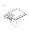
- FIG. 1 is a schematic perspective view of a display device according to an embodiment of the present invention.
- 1 is a schematic plan view of a display device according to an embodiment of the present invention.
- 1 is a circuit diagram of a pixel included in a display device according to an embodiment of the present invention.
- 4 is a timing chart of pixels included in a display device according to an embodiment of the present invention.
- 4 is a timing chart of pixels included in a display device according to an embodiment of the present invention.
- FIG. 6 is a schematic diagram illustrating a state of a pixel included in a display device according to an embodiment of the present invention for each period. 4 is a timing chart of pixels included in a display device according to an embodiment of the present invention.
- FIG. 1 is a schematic perspective view of a display device according to an embodiment of the present invention.
- 1 is a schematic plan view of a display device according to an embodiment of the present invention.
- 1 is a circuit diagram of a pixel included in a display device according to
- FIG. 6 is a schematic diagram illustrating a state of a pixel included in a display device according to an embodiment of the present invention for each period.
- 1 is a circuit diagram of a pixel included in a display device according to an embodiment of the present invention.
- 4 is a timing chart of pixels included in a display device according to an embodiment of the present invention.
- 1 is a circuit diagram of a pixel included in a display device according to an embodiment of the present invention.
- 4 is a timing chart of pixels included in a display device according to an embodiment of the present invention.
- 1 is a circuit diagram of a pixel included in a display device according to an embodiment of the present invention.
- 4 is a timing chart of pixels included in a display device according to an embodiment of the present invention.
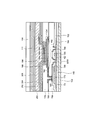
- 1 is a schematic cross-sectional view of a pixel included in a display device according to an embodiment of the present invention.
- the first substrate described in this specification has at least one planar main surface, and each element such as an insulating layer, a semiconductor layer, and a conductive layer, or a transistor and a display element is formed on the one main surface.
- each element such as an insulating layer, a semiconductor layer, and a conductive layer, or a transistor and a display element is formed on the one main surface.
- an EL display device has a plurality of pixels formed on a substrate.
- Each of the plurality of pixels includes a driving transistor, a capacitor element, a light emitting element, and an additional capacitor included in the light emitting element.
- the additional capacitance included in the light emitting element includes, for example, a case where the light emitting element itself having a diode characteristic also has a capacitance component.
- Each pixel supplies a light-emitting current to the light-emitting element by controlling the driving of the driving transistor with a signal, and the display device can display an image when the light-emitting element emits light. That is, the light emitting element becomes brighter or darker depending on the magnitude of the light emission current.
- the magnitude of the light emission current depends on the amount of current that the drive transistor flows to the light emitting element. More specifically, a charge corresponding to the amount of current flowing through the drive transistor is stored in the capacitor element and the additional capacitor, and the magnitude of the light emission current depends on the amount of the stored charge.
- the capacitance value of the capacitor or the additional capacitor is increased, the maximum value of the light emission current that can be supplied to the light emitting element can be increased without increasing the voltage applied to the capacitor or the additional capacitor.
- a capacitance value larger than the capacitance value of the pixel in other words, the capacitance element included in the pixel or the capacitance value of the additional capacitor is ensured in the light-emitting element.
- the maximum value of the light emission current that can be supplied can be increased. Further, since the display device of the present invention can increase the maximum value of the light emission current, the dynamic range of the pixel can be widened. Specifically, in a plurality of pixels included in the display device, before the light emitting element of the first pixel emits light, a light emitting element electrically connected to the driving transistor of the first pixel and an additional capacitor included in the light emitting element The light emitting element included in the second pixel adjacent to the first pixel and the additional capacitor included in the light emitting element are electrically connected by the capacitance control transistor of the first pixel.
- the driving transistor is electrically connected to the power supply line, and a video signal of the first pixel is supplied to the driving transistor of the first pixel, so that a current flows through the driving transistor of the first pixel, which corresponds to the flowing current value.
- Charge is stored in each additional capacity.
- the maximum value of the charge that can be stored based on the video signal of the first pixel can be increased by the amount of additional capacitance of the adjacent pixel that is used to hold the charge, as compared with the conventional case. That is, a large light emission current can be supplied to the light emitting element included in the first pixel. Therefore, according to the present invention, it is possible to provide a display device capable of securing a large light emission current when the pixel emits light, and to provide a display device having a pixel with a wide dynamic range.
- FIG. 1 is a schematic perspective view of a display device 100 according to an embodiment of the present invention.
- the display device 100 includes a first substrate 102, a filler 111, and a second substrate 104.
- the first surface of the first substrate 102 includes a display region 106, a scanning signal line driver circuit 118, a video signal line driver circuit (driver IC) 120, a control circuit 122, and a terminal region 114 having a plurality of terminal electrodes 116.
- the display device 100 may have a structure in which the second substrate 104 is not provided. For example, a structure in which a protective film is bonded to a side where the display region 106 of the first substrate 102 is positioned or a structure in which a circularly polarizing plate is bonded may be used.
- the display area 106 has a plurality of pixels 108.
- the plurality of pixels 108 are arranged along one direction and a direction intersecting with one direction.
- the number of pixels 108 arranged is arbitrary. For example, n pixels 108 are arranged in the row direction and m pixels 108 are arranged in the column direction. n and m are each a natural number of 2 or more.
- a plurality of terminal electrodes 116 are connected to a display substrate 100 and a device that outputs a video signal, a timing signal for controlling operations of the scanning signal line driver circuit 118 and the video signal line driver circuit 120, and the power source (see FIG. Not shown) is connected.
- the wiring board is, for example, a flexible printed circuit board (FPC).
- FPC flexible printed circuit board
- Each of the plurality of pixels 108 can be provided with a plurality of subpixels.
- one pixel includes three sub-pixels, and the three sub-pixels include a sub-pixel including a display element corresponding to red (R), a sub-pixel including a display element corresponding to green (G), It consists of a sub-pixel provided with a display element corresponding to blue (B).
- a color display device can be provided by supplying multi-level voltages or currents of, for example, 256 levels to each of the three sub-pixels, in other words, by inputting video signals of 256 gradations. .
- One sub-pixel may be simply referred to as a pixel.
- a display device in which one pixel includes one display element and can perform monochrome display or white and black gradation display can be provided.
- the arrangement of the plurality of pixels 108 is not limited, and a stripe arrangement, a delta arrangement, or the like can be employed.
- the display element provided in the pixel 108 is a light emitting element will be described.
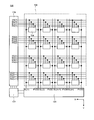
- FIG. 2 is a schematic plan view of the display device 100 according to an embodiment of the invention.
- the display device 100 is an active matrix EL display device. Each pixel 108 has a light emitting element.
- a video signal, a timing signal for controlling the operation of the circuit, and power are supplied to the control circuit 122 through the plurality of terminal electrodes 116 shown in FIG.
- the control circuit 122 supplies each signal and power supply voltage to the scanning signal line driving circuit 118 and the video signal line driving circuit 120.
- the control circuit 122 generates a new signal or power supply voltage from each signal or power supply voltage using a logic circuit (not shown) or a voltage generation circuit (not shown) included in the control circuit 122, and scan signal line driving.
- the signal may be supplied to the circuit 118 or the video signal line driver circuit 120.
- the position where the control circuit 122 is disposed is not limited to the first substrate 102 shown in FIG.
- the control circuit 122 may be located on a wiring board connected to the terminal electrode 116.
- the scanning signal line driver circuit 118 and the video signal line driver circuit 120 drive the light emitting element included in the pixel 108 using each signal and power supply voltage supplied from the control circuit and cause the light emitting element to emit light, thereby displaying the display region.
- 106 plays a role of displaying an image.
- the scanning signal line driving circuit 118 supplies a scanning signal to the plurality of pixels 108 located in the n-th row configured in the display region 106 via the scanning signal line SG (n) in common, and the control line RG ( The control signal is supplied via n), the emission control signal is supplied via the emission control signal line BG (n), and the capacitance control signal is supplied via the capacitance control signal line EG (n).
- the video signal line driving circuit 120 outputs a video signal and an initialization signal to the plurality of pixels 108 in the m-th column configured in the display area 106 in common via the video signal line SL (m). It is configured to be supplied in splits.
- the potential of the video signal is denoted as Vsig (m)
- the potential of the initialization signal is denoted as Vini. Vini may be called an initialization potential.
- the video signal is determined according to video data displayed in the display area 106, and its potential Vsig (m) is adjusted by a correction method described later.
- the potential Vini of the initialization signal can be a fixed potential.
- the video signal line drive circuit 120 is further configured to give a bias signal to a plurality of pixels located in the m-th column via the bias line VL shown in FIG.
- the potential of the bias signal is denoted as Vrst. Note that an example in which the potential Vrst of the bias signal is a fixed potential is shown, but the potential of the bias signal may vary with time.
- the video signal line driving circuit 120 is further configured to supply a high potential and a low potential to each pixel 108 via the high potential power supply wiring PVDD.
- a high potential supplied from the high potential power supply wiring PVDD is referred to as VDD_H, and a low potential is referred to as VDD_L.
- VDD_H A high potential supplied from the high potential power supply wiring PVDD
- VDD_L a low potential
- a common electrode provided in common for the plurality of pixels 108 and connected to the low potential power wiring PVSS is disposed in the display region 106.
- the video signal line driving circuit 120 is configured to supply a fixed potential VSS to the common electrode.
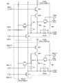
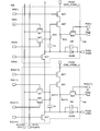
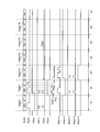
- FIG. 3 is a pixel circuit diagram 300 included in the pixel 108 according to an embodiment of the present invention.
- a pixel circuit diagram 300 shown in FIG. 3 shows two pixels 108 arranged in an n-row and m-column and an n + 1 row and m-column arranged in the display area 106.
- Each of the two pixels 108 shown in FIG. 3 includes one light emitting element OLED. Therefore, the two pixels 108 illustrated in FIG. 3 may be two adjacent sub-pixels.
- the pixel 108 includes a capacitance control transistor ECT (first switch), a selection transistor SST (second switch), a driving transistor DRT, a selection transistor SST (third switch), and an initialization transistor RST (fourth switch).
- Switch a light emission control transistor BCT (fifth switch), a capacitor element Cs, a light emitting element OLED, and an additional capacitor Cel.
- Each of these transistors has a gate and a pair of terminals (an input / output terminal, a source electrode and a drain electrode) including a first terminal and a second terminal, and the capacitor Cs has a pair of terminals (a first terminal and a first terminal).
- the additional capacitor Cel has a pair of terminals (a first terminal and a second terminal).
- FIG. 2 shows an example in which the additional capacitor Cel is provided in parallel with the light emitting element OLED, but the present invention is not limited to this.
- the additional capacitor Cel may be a parasitic capacitance of the light emitting element OLED, or may include a capacitive element provided in parallel with the light emitting element OLED and a parasitic capacitance of the light emitting element OLED.
- the driving transistor DRT has a role of causing the light emitting element OLED to emit light by causing a current to flow through the light emitting element OLED based on the input video signal.
- the selection transistor SST has a role of supplying a video signal and an initialization signal to the driving transistor DRT.
- the initialization transistor RST has a role of supplying a bias signal to the driving transistor DRT, the light emitting element OLED, and the additional capacitor Cel, and initializing a circuit included in each pixel 108.
- the light emission control transistor BCT controls connection / disconnection of the drive transistor DRT and the high potential power supply wiring PVDD. That is, the light emission control transistor BCT has a role of controlling light emission and non-light emission of the light emitting element OLED.
- the capacitance control transistor ECT includes the light emitting element OLED and the additional capacitor Cel included in the pixel, for example, the pixel 108 positioned in the n row and m column, and the light emission included in the pixel adjacent to the pixel, for example, the pixel 108 positioned in the n + 1 row and m column.
- the element OLED and the additional capacitor Cel are electrically connected to increase the capacitance value and to increase the maximum amount of current that can be supplied to the light emitting element of the pixel.
- the capacitive element Cs maintains a potential corresponding to the threshold value of the drive transistor DRT and maintains a potential input to the gate of the drive transistor DRT so that the pixel 108 emits light, that is, an input video signal is described in detail.
- the light emitting element OLED has a diode characteristic and includes a pixel electrode, the above-described common electrode, and a light emitting layer (EL layer, organic layer) positioned between the pixel electrode and the common electrode.
- the additional capacitor Cel is a capacitor included in the light emitting element OLED. The video signal input by the additional capacitor Cel and the capacitor element Cs may be held.
- the gate of the selection transistor SST is electrically connected to the scanning signal line SG (n), the first terminal is electrically connected to the video signal line SL (m), and the second terminal is the gate of the driving transistor DRT.
- the first terminal of the drive transistor DRT is electrically connected to the second terminal of the light emission control transistor BCT, the second terminal is the input terminal (or pixel electrode) of the light emitting element OLED, and the second terminal of the initialization transistor RST.
- the second terminal and the second terminal of the storage capacitor Cs are electrically connected.
- the gate of the light emission control transistor BCT is electrically connected to the light emission control signal line BG (n), and the first terminal is electrically connected to the high potential power supply wiring PVDD.
- the first terminal of the additional capacitor Cel is electrically connected to the second terminal of the drive transistor DRT, and the second terminal of the additional capacitor Cel is electrically connected to the low potential power supply line PVSS.
- the output terminal (or common electrode) of the light emitting element OLED is electrically connected to the low potential power wiring PVSS.
- a fixed potential VSS is applied to the low potential power wiring PVSS.
- the fixed potential VSS only needs to be a fixed potential lower than the low potential VDD_L, and can be, for example, a ground potential.
- the first terminal of the initialization transistor RST is electrically connected to the bias line VL, and the gate is electrically connected to the control line RG (n).
- the gate of the capacitance control transistor ECT is electrically connected to the capacitance control signal line EG (n), the first terminal is the second terminal of the capacitance element Cs, the input terminal of the light emitting element OLED, and the first of the additional capacitance Cel. , The second terminal of the initialization transistor RST, and the second terminal of the driving transistor DRT.
- the second terminals of the capacitance control transistors ECT are the first terminals of the (n + 1) th row capacitance control transistors ECT, the second terminals of the (n + 1) th row capacitance elements Cs, the input terminals of the (n + 1) th row light emitting elements OLED, and the (n + 1) th row.
- Each transistor shown in FIG. 3 can have a group 14 element such as silicon or germanium or an oxide exhibiting semiconductor characteristics in a channel region.
- the oxide include oxides containing group 13 elements such as indium-gallium oxide (IGO) and indium-gallium-zinc (IGZO).
- IGO indium-gallium oxide
- IGZO indium-gallium-zinc
- these transistors are all described as n-channel field effect transistors, but some or all of these transistors may be p-channel field effect transistors.
- the channel region of these transistors can have various morphologies selected from single crystal, polycrystal, microcrystal, or amorphous. For example, low-temperature polysilicon (LTPS) obtained by melting and recrystallizing amorphous silicon at a relatively low temperature can be included.
- LTPS low-temperature polysilicon
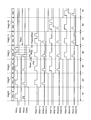
- FIG. 4 is a timing chart of a pixel included in the display device according to the embodiment of the present invention, and shows a time change of each signal shown in FIG.
- FIG. 4 also shows a timing chart of the pixel of n + 1 rows and m columns, but the basic operation is the same as that of the pixels of n rows and m columns.
- the activation state of each transistor is described in association with the high level. However, whether the high level or the low level is referred to as the activation state is arbitrary for each signal.
- an activated state or an activated state means a state where a source and a drain of a transistor are conductive, a state where a current flows between the source and the drain, and a state where a transistor is on.
- an inactivated state or an inactivated state means a state where a source and a drain of a transistor are non-conductive, a state where no current flows between the source and the drain, and a state where a transistor is off.
- the n rows and m columns of pixels include three operations within one horizontal period (horizontal scanning period). These are, in order, a reset operation, a threshold correction (threshold voltage variation correction) operation, a current correction (mobility variation correction), and a write operation. After these operations, the light emitting element OLED emits light over a plurality of horizontal periods following the one horizontal period.
- the periods corresponding to these operations are referred to as a reset period Prst, a threshold correction period Pcom, a current correction and writing period Pccom + Pwrt, and a light emission period Pemi, respectively.
- Each horizontal period is indicated by 1H, 2H, 3H, 4H, 5H, 6H, and 7H.
- a low level is supplied from the light emission control signal line BG (n) to the gate of the light emission control transistor BCT in the n rows and m columns, and the light emission control in the n + 1 rows and m columns from the light emission control signal line BG (n + 1).
- a low level is supplied to the gate of the transistor BCT, and both the light emission control transistors BCT in the nth row and mth column and the n + 1th row and mth column are turned off.
- the pixels in n rows and m columns and the pixels in n + 1 rows and m columns are in a dark state.
- the signal supplied from the scanning signal line SG (n) to the gate of the selection transistor SST in the n rows and m columns is changed from the low level to the high level, and the selection transistors SST in the n rows and m columns are turned on, as shown in FIG. Vini is written to node A (n).
- the signal supplied from the control line RG (n) to the gate of the initialization transistor RST in the n row and m column is changed from the low level to the high level, and the initialization transistor RST in the n row and m column is turned on, as shown in FIG. Vrst is written to the node B (n).
- the signal supplied from the capacitance control signal line EG (n) to the gate of the capacitance control transistor ECT of n rows and m columns is at a high level, and the capacitance control transistor ECT of n rows and m columns is on.
- Node B (n) and node B (n + 1) shown in FIG. 3 are brought into conduction, and Vrst is written to the node B (n + 1).
- the signal supplied from the scanning signal line SG (n + 1) to the gate of the selection transistor SST in the n + 1 row and m column is changed from the low level to the high level, and the selection transistor SST in the n + 1 row and m column is turned on.
- the initialization transistor RST of n + 1 rows and m columns may be on or off. That is, the signal on the control line RG (n + 1) may be at a high level or a low level. Further, writing Vini to the node A (n), writing Vini to the node A (n + 1), and writing Vrst to the node B (n) may be performed simultaneously.
- the potentials of the node A (n) in the nth row and mth column and the node A (n + 1) in the n + 1th row and mth column are set to Vini
- the node B (n) in the nth row and mth column is set to the n + 1th row m.
- the potential of node B (n + 1) in the column is set to Vrst. That is, the potential between the first terminal and the second terminal of the capacitor element in n rows and m columns is the same as the potential between the first terminal and the second terminal of each capacitor element in n + 1 rows and m columns. To. That is, it is possible to initialize the potential between the gate and the second terminal of the driving transistor DRT of n rows and m columns and the potential between the gate and the second terminal of the driving transistor DRT of n + 1 rows and m columns.
- the threshold correction operation will be described.
- the signal supplied from the control line RG (n) to the gate of the initialization transistor RST in n rows and m columns is changed from the high level to the low level, and the initialization transistor RST is turned off.
- Both the selection transistor SST of n rows and m columns and the selection transistor SST of n + 1 rows and m columns are kept on, and the potentials of the nodes A (n) and A (n + 1) are kept at Vini.
- the capacitance control transistor ECT of n rows and m columns maintains the on state, and the potentials of the node B (n) and the node B (n + 1) are maintained at Vrst.
- the signal supplied from the light emission control signal line BG (n) to the gate of the light emission control transistor BCT in the n rows and m columns is changed from the low level to the high level, and the light emission control transistors BCT in the n rows and m columns are turned on.
- VDD_H is supplied from the high potential power supply wiring PVDD to the drive transistor DRT of n rows and m columns via the light emission control transistor BCT.
- a current flows through the driving transistor DRT of n rows and m columns, and the potential of the node B (n) is shifted from Vrst to the high potential side.
- the threshold voltage Vthn of the driving transistor DRT of n rows and m columns can be held between the terminals.
- a write operation to be described later is performed from the state in which the threshold voltage Vthn is held in the capacitor element Cs. Therefore, even if there is a variation in the threshold voltage of each of the drive transistors DRT included in each of the plurality of pixels 108, the variation in the threshold voltage is removed when the light emitting element OLED included in each of the plurality of pixels 108 emits light. Can do.
- a signal supplied from the scanning signal line SG (n) to the gate of the selection transistor SST in the n rows and m columns is changed from the high level to the low level, and the selection transistors SST in the n rows and m columns are turned off. Further, the signal supplied from the scanning signal line SG (n + 1) to the gate of the selection transistor SST in the n + 1 row and m column is also changed from the high level to the low level, and the selection transistor SST in the n + 1 row and m column is also turned off.
- the capacitance control transistor ECT of n rows and m columns maintains the on state. At this time, the potentials of the node B (n) and the node B (n + 1) are kept at Vini ⁇ Vthn.
- the light emission control transistor BCT in the n rows and m columns maintains the on state.
- the initialization transistor RST is kept off.
- the capacitance control transistor ECT in n rows and m columns maintains the on state.
- the potentials of the nodes B (n) and B (n + 1) are kept at Vini ⁇ Vthn.
- the light emission control transistor BCT in the n rows and m columns maintains the on state.
- the initialization transistor RST is kept off.
- the signal supplied from the scanning signal line SG (n) to the gate of the selection transistor SST in the n rows and m columns is changed from the low level to the high level, and the selection transistors SST in the n rows and m columns are turned on.
- Vsig (m) is supplied from the video signal line SL (m) electrically connected to the first terminal of the selection transistor SST, and the potential of the node A (n) is changed from Vini to Vsig (m). That is, Vsig (m) is written to the node A (n). Since the gate voltage of the driving transistor DRT of n rows and m columns is also Vsig (m), the driving transistor DRT is turned on, and a current flows through the driving transistor DRT. Note that the input terminal of the light emitting element OLED of n rows and m columns and n + 1 rows and m columns and the first terminal of the additional capacitor Cel of n rows and m columns and n + 1 rows and m columns are electrically connected to the node B (n). ing.
- the potential of the node B (n) that is, the potential of the input terminal of the light emitting element OLED (here, the anode voltage of the light emitting element OLED) is the light emitting element. It is smaller than the threshold voltage of the OLED, and no current flows to the light emitting element OLED. Alternatively, the light emitting element OLED does not emit light.
- the voltage of the second terminal of the driving transistor DRT of n rows and m columns that is, the potential of the node B (n) increases.
- the potential increase of the node B (n) here also increases.
- the increased potentials of the nodes B (n) and B (n + 1) are expressed by the following formula (1) due to capacitive coupling via the capacitive element Cs included in the pixel of n rows and m columns.
- a (n) represents the potential of the node A (n)
- B (n) represents the potential of the node B (n).
- the potential difference (gate-source voltage) between the gate and the second terminal of the driving transistor DRT of n rows and m columns, that is, the potential difference between the node A (n) and the node B (n) is expressed by the following equation (2 ).
- the capacitor Cs of n rows and m columns holds the voltage shown in the equation (2).
- the current Id flowing from the first terminal to the second terminal of the driving transistor DRT of n rows and m columns is expressed by the following equation (3).
- ⁇ is a gain coefficient of the driving transistor DRT of n rows and m columns.
- the video signal can be written and the current of the driving transistor DRT can be corrected.
- the input terminal of the light emitting element OLED of n rows and m columns and n + 1 rows and m columns and the first terminal of the additional capacitor Cel of n rows and m columns and n + 1 rows and m columns are electrically connected by the capacitance control transistor ECT.
- the additional capacitor Cel in the (n + 1) rows and m columns can also contribute.
- the additional capacitance of the adjacent pixel here, the additional capacitance Cel of the pixel 108 in the n + 1 row and m column can be shared.
- the embodiment shows the potential difference between the node A (n) and the node B (n) as shown in Expression (2). That is, the gate-source voltage of the drive transistor DRT can be increased, and a high dynamic range can be realized.
- the light emission control transistor BCT in n rows and m columns maintains the on state.
- the initialization transistor RST is kept off.
- a signal supplied from the capacitance control signal line EG (n) to the gate of the capacitance control transistor ECT of n rows and m columns is changed from a high level to a low level, and the capacitance control transistor ECT of the n rows and m columns is turned off.
- the node B (n) and the node B (n + 1) are separated by turning off the capacitance control transistor ECT.
- a signal supplied from the scanning signal line SG (n) to the gate of the selection transistor SST in the n rows and m columns is changed from the high level to the low level, and the selection transistors SST in the n rows and m columns are turned off.
- the driving transistor DRT of n rows and m columns supplies current to the light emitting element OLED based on the voltage held in the capacitive element Cs. Therefore, light emission of the light emitting element OLED of n rows and m columns is started.
- the light emission current at this time is expressed by Equation (4).
- the light emission current is small because the capacitance value is only for the additional capacitance Cel of n rows and m columns.
- the first terminal of the additional capacitor Cel of n rows and m columns and n + 1 rows and m columns is electrically connected by the capacitance control transistor ECT, so that the additional capacitor Cel of n + 1 rows and m columns is shared. ing. Therefore, compared to the conventional case, when a video signal is input to the pixel 108 in the n row and m column, the capacity used by the pixel 108 is larger because the additional capacitor Cel included in the pixel 108 in the n + 1 row and m column is shared. Become.
- the fractional part of the expressions (2) and (4) becomes Cel / Cs + Cel when there is no capacitance control transistor ECT, but in the present invention, as shown in the expressions (2) and (4). 2Cel / Cs + 2Cel. Therefore, the maximum value of the light emission current that can flow to the light emitting element OLED can be increased.
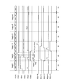
- FIG. 5 is a timing chart of pixels included in the display device according to the embodiment of the present invention.
- the timing chart of n + 2 rows and m columns and n + 3 rows and m columns is added to the timing chart of FIG.
- Each horizontal period is indicated by 1H, 2H, 3H, 4H, 5H, 6H, and 7H.
- the operations of the reset period Prst, the threshold correction period Pcom, the current correction and writing period Pccom + Pwrt, and the light emission period Pemi described above are sequentially repeated from the nth row mth column to the n + 3th row mth column shown in FIG.
- the current of the light emitting element included in the display device can be increased, and a high dynamic range can be realized.
- FIG. 6 is a schematic diagram showing the state of the pixels included in the display device according to the embodiment of the present invention for each horizontal period.
- FIG. 6 shows the operation state in each horizontal period shown in the timing chart of FIG. 5 from n rows to m columns to n + 3 rows and m columns, followed by n + 4 rows to m columns to n + 6 rows and m columns.
- Each horizontal period is indicated by 1H, 2H, 3H, 4H, 5H, and 6H.
- periods Prst to Pwrt indicate periods during which the above-described reset period Prst, threshold correction period Pcom, current correction and write period Pccom + Pwrt are performed.
- the capacitance control transistor ECT in the previous row electrically connects the capacitance Cs and the additional capacitance Cel included in the pixel in the previous row to the additional capacitance Cel included in the own pixel. It shows the period of the status. In other words, the state in which the adjacent pixels share the capacitance is shown.
- the additional capacitance Cel of the pixel in the (n + 2) th row and the mth column is electrically connected to the capacitance element Cs and the additional capacitance Cel included in the pixel in the (n + 1) th row and the mth column.
- one pixel has a period Cshr, a reset period Prst, and a threshold correction period in which the additional capacitor Cel included in the pixel is electrically connected to the capacitor Cs included in the pixel in the previous row and the additional capacitor Cel.
- Pcom current correction and writing period Pccom + Pwrt, and light emission period Pemi
- the horizontal period before the period Cshr may be the light emission period Pemi in the previous frame period.
- the capacitance control transistor ECT is provided, and the input terminal of the n-row m-column light emitting element OLED and the first terminal of the additional capacitor Cel, and the input terminal of the n + 1 row m-column light-emitting element OLED and the additional capacitor Cel of A large capacity can be secured by being electrically connected to the first terminal. Therefore, the current of the light emitting element can be increased and a high dynamic range can be realized.
- the capacitance (capacitance element Cs and additional capacitance Cel) included in the pixel is also reduced. Accordingly, the voltage held by the capacitor is reduced, and the maximum value of the current that can be passed to the light emitting element is also reduced.
- the capacitive element Cs and the additional capacitor Cel included in the pixel 108 in the n row and m column and the additional capacitor Cel included in the pixel 108 in the n + 1 row and m column are shared, so that the current flows to the light emitting element OLED. It is possible to prevent the maximum value of the possible current from becoming small. That is, it is possible to flow a sufficient amount of current to the light emitting element OLED.
- the display device can display with high gradation. Therefore, the display device and the driving method described above can provide a high-definition display device with high display quality.
- the pixel circuit in the second embodiment is the same as the pixel circuit shown in the pixel circuit diagram 300 of FIG.
- the capacitance control transistor ECT included in the pixel 108 in n rows and m columns and the capacitance control transistor ECT included in the pixel 108 in n + 1 rows and m columns are simultaneously turned on, so that n + 3 to n + 3
- a description will be given of sharing the additional capacitor Cel included in the pixel 108 in the row m column, securing a larger light emission current, and realizing a higher dynamic range.
- description may be abbreviate
- FIG. 7 is a timing chart of the pixels 108 from n rows and m columns to n + 3 rows and m columns included in the display device according to the embodiment of the present invention. Each horizontal period is indicated by 1H, 2H, 3H, 4H, 5H, 6H, and 7H.
- a high level signal is supplied from the capacitance control signal line EG (n) to the gate of the capacitance control transistor ECT in the nth row and mth column, and the capacitance control transistor ECT in the nth row and mth column is turned on.
- a high level signal is supplied from the capacitance control signal line EG (n + 1) to the gate of the capacitance control transistor ECT in the (n + 1) th row and the mth column, and the capacitance control transistor ECT in the (n + 1) th row and the mth column is turned on.
- a high level signal is supplied from the capacitance control signal line EG (n + 2) to the gate of the capacitance control transistor ECT of n + 2 rows and m columns, and the capacitance control transistor ECT of n + 2 rows and m columns is turned on.
- a high level signal is supplied from the capacitance control signal line EG (n + 3) to the gate of the capacitance control transistor ECT of n + 3 rows and m columns, and the capacitance control transistor ECT of n + 3 rows and m columns is turned on.
- the first terminal of the additional capacitor Cel in the row m column and the first terminal of the additional capacitor Cel in the (n + 3) row m column are electrically connected. Therefore, the potential difference (gate-source voltage) between the gate and the second terminal of the driving transistor DRT of n rows and m columns, that is, the potential difference between the node A (n) and the node B (n) is expressed by the following equation (5). It is represented by
- the current Id flowing from the first terminal to the second terminal of the driving transistor DRT of n rows and m columns is expressed by the following equation (6).
- ⁇ is a gain coefficient of the driving transistor DRT of n rows and m columns.
- the current Id flowing from the first terminal to the second terminal of the drive transistor DRT does not depend on the threshold value of the drive transistor DRT.
- the video signal can be written and the current of the driving transistor DRT can be corrected.
- the capacitance control transistor ECT electrically connects the input terminal of the light emitting element OLED from n rows to m columns to n + 3 rows and m columns and the first terminal of the additional capacitor Cel from n rows to m columns to n + 3 rows and m columns.
- the additional capacitor Cel included in the pixels 108 in the n + 1 rows and m columns to the n + 3 rows and m columns can be shared.
- the gate-source voltage of the drive transistor DRT can be further increased as compared with the first embodiment, and a higher dynamic range can be realized.
- the light emission control transistor BCT in n rows and m columns maintains the on state.
- the initialization transistor RST is kept off.
- a signal supplied from the capacitance control signal line EG (n) to the gate of the capacitance control transistor ECT of n rows and m columns is changed from a high level to a low level, and the capacitance control transistor ECT of the n rows and m columns is turned off.
- the node B (n) and the node B (n + 1) to the node B (n + 3) are separated by turning off the capacitance control transistor ECT.
- a signal supplied from the scanning signal line SG (n) to the gate of the selection transistor SST in the n rows and m columns is changed from the high level to the low level, and the selection transistors SST in the n rows and m columns are turned off.
- the driving transistor DRT of n rows and m columns supplies current to the light emitting element OLED based on the voltage held in the capacitive element Cs. Accordingly, the light emitting elements of n rows and m columns start to emit light.
- the light emission current at this time is expressed by Expression (6).
- the light emission current is small because the capacitance value is only for the additional capacitance Cel of n rows and m columns.
- the capacity used by the pixel 108 is the additional capacitor Cel included in the pixel 108 in the n + 1 row m column to the n + 3 row m column. It grows as much as you share. Therefore, the maximum value of the light emission current that can flow to the light emitting element OLED can be increased.
- FIG. 8 is a schematic diagram showing the state of the pixels included in the display device according to the embodiment of the present invention for each horizontal period.
- Each horizontal period is indicated by 1H, 2H, 3H, 4H, 5H, and 6H.
- periods Prst to Pwrt indicate periods during which the above-described reset period Prst, threshold correction period Pcom, current correction and write period Pccom + Pwrt are performed.
- a period Cshr in the figure shows a state in which the additional capacitor Cel is shared by adjacent pixels, for example, the pixels 108 in the n-th row and m-th column to the (n + 3) -th row and m-column by the capacitance control transistor ECT.
- the pixel in the (n + 2) th row and the mth column is in a state in which a reset operation, a threshold correction operation, a current correction, and a write operation are performed in the period H3.
- the additional capacitor Cel included in each pixel is electrically connected by the capacitance control transistor ECT included in the four pixels of n rows and m columns, n + 1 rows and m columns, n + 2 rows and m columns, and n + 3 rows and m columns.
- the additional capacitor Cel included in each pixel is electrically connected by the capacitance control transistor ECT included in the three pixels of n rows and m columns, n + 1 rows and m columns, and n + 2 rows and m columns. Also good.
- the capacitance control transistor ECT is provided, and the input terminal of the light emitting element OLED from n rows to m columns to n + 3 rows and m columns and the first terminal of the additional capacitor Cel from n rows to m columns to n + 3 rows and m columns are electrically connected.
- the larger capacity can be ensured by connecting them in the same manner. Therefore, the current of the light emitting element can be further increased and a higher dynamic range can be realized. Therefore, even in a display device having a small pixel size, a large current for the light emitting element to emit light can be supplied, and a reduction in luminance of the display device can be suppressed.
- the display device can realize high gradation display. Therefore, the display device and the driving method described above can provide a high-definition display device with high display quality.
- the present embodiment further includes an initialization signal input transistor IST.
- description may be abbreviate
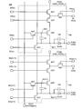
- FIG. 9 is a pixel circuit diagram 400 provided in the pixel 108 included in the display device according to the embodiment of the present invention.
- the pixel circuit diagram 400 shows two pixels 108 arranged in the display area 106 in n rows and m columns and n + 1 rows and m columns.
- the pixel 108 has a configuration in which the pixel circuit diagram 300 shown in FIG. 3 further includes an initialization signal input transistor IST.
- each transistor has a gate and a pair of terminals (first terminal and second terminal), and the capacitor Cs has a pair of terminals (first terminal and second terminal).
- the additional capacitor Cel has a pair of terminals (a first terminal and a second terminal).
- capacitance Cel it may be a parasitic capacity
- the configuration changed from FIG. 3 will be described. Since the configuration other than the change is the same as that of FIG. 3, the description thereof is omitted here.
- the gate of the initialization signal input transistor IST is electrically connected to the initialization signal control line IG (n), the first terminal is electrically connected to the initialization signal line SL2 (m), and the second terminal Are electrically connected to the gate of the drive transistor DRT, the second terminal of the selection transistor SST, and the first terminal of the capacitor Cs.
- the potential Vini of the initialization signal is input from the video signal line SL (m) to the pixel 108 (to the selection transistor SST).
- Vini is input from the initialization signal line SL2 (m) to the initialization signal input transistor IST.
- the pixel of n rows and m columns among the pixels 108 included in the pixel circuit has been described.
- the configuration of the pixel in the n + 1 row and the m column is the same as that of the pixel in the n row and the m column.
- FIG. 10 is a timing chart of a pixel included in the display device according to the embodiment of the present invention, and shows a time change of each signal shown in FIG.
- FIG. 10 also shows a timing chart of pixels of n + 1 rows and m columns, but the basic operation is the same as that of pixels of n rows and m columns.
- the reset operation, the threshold value, and the reset period Prst, the threshold value correction period Pcom, the current correction and writing period Pccom + Pwrt, and the light emission period Pemi are performed, respectively.
- the initialization signal input transistor IST Prior to the reset operation, the initialization signal input transistor IST is turned on by supplying a high level from the initialization signal line IG (n) to the gate of the initialization signal input transistor IST in n rows and m columns, as shown in FIG.
- An operation of writing Vrst to the node B (n) may be performed. Both of these two operations may be performed, or any one of these two operations may be performed.
- Vini in 1H and Vsig (d) in 1H may be the same.
- a low level is supplied from the light emission control signal line BG (n) to the gate of the light emission control transistor BCT in the n rows and m columns, and the light emission control in the n + 1 rows and m columns from the light emission control signal line BG (n + 1).
- a low level is supplied to the gate of the transistor BCT, and both transistors are turned off. At this time, the pixels in n rows and m columns and the pixels in n + 1 rows and m columns are in a dark state.
- a high level signal is supplied from the initialization signal control line IG (n) to the gate of the initialization signal input transistor IST in the nth row and mth column, and the initialization signal input transistor IST in the nth row and mth column is turned on. Further, a high level signal is supplied from the initialization signal control line IG (n + 1) to the gate of the initialization signal input transistor IST in the (n + 1) th row and the mth column, and the initialization signal input transistor IST in the (n + 1) th row and the mth column is turned on. As a result, Vini is written to the nodes A (n) and A (n + 1) shown in FIG.
- a low level signal is supplied from the scanning signal line SG (n) to the gate of the selection transistor SST of n rows and m columns, and the selection transistor SST of the n rows and m columns is off.
- a low level signal is supplied from the scanning signal line SG (n + 1) to the gates of the selection transistors SST in the (n + 1) rows and m columns, and the selection transistors SST in the (n + 1) rows and m columns are inactivated. Is off.
- the signal supplied from the control line RG (n) to the gate of the initialization transistor RST in the n rows and m columns is changed from the low level to the high level, so that the initialization transistor RST in the n rows and m columns is turned on. Vrst is written in (n).
- the signal supplied from the capacitance control signal line EG (n) to the gate of the capacitance control transistor ECT of n rows and m columns is changed from the low level to the high level, and the capacitance control transistor ECT of the n rows and m columns is turned on.
- Vrst is written to the node B (n + 1) shown in FIG.
- the initialization transistor RST of n + 1 rows and m columns may be on or off. Further, writing Vini to the node A (n), writing Vini to the node A (n + 1), and writing Vrst to the node B (n) may be performed simultaneously.
- the operation of setting the potential of the node A (n) in the nth row and mth column and the node A (n + 1) in the n + 1th row and mth column to Vini which is performed by the selection transistor SST.
- the initialization signal input transistor IST takes charge.
- the selection transistor SST is responsible for the operation of writing the video signal to the gate of the drive transistor DRT, and the initialization signal input transistor IST is responsible for the above-described operation, so that the time for the write operation and the time for the initialization signal input operation are sufficient. Can be secured, and the driving of the pixel can be stabilized.
- the threshold correction operation will be described. Subsequent to the reset operation, the signal supplied from the control line RG (n) to the gate of the initialization transistor RST in n rows and m columns is changed from the high level to the low level, and the initialization transistor RST is turned off. Both the n-row and m-column selection transistor SST and the (n + 1) row and m-column selection transistor SST maintain the OFF state. Both the initialization signal input transistors IST of the n-th row and the m-th column and the (n + 1) -th row and the m-th column maintain the on state. The potentials of the nodes A (n) and A (n + 1) are kept at Vini.
- the capacitance control transistor ECT of n rows and m columns maintains the on state, and the potentials of the node B (n) and the node B (n + 1) are maintained at Vrst.
- a high level signal is supplied from the light emission control signal line BG (n) to the gate of the light emission control transistor BCT in the n rows and m columns, and the light emission control transistors BCT in the n rows and m columns are turned on.
- VDD_H is supplied from the high potential power supply wiring PVDD to the drive transistor DRT of n rows and m columns via the light emission control transistor BCT.
- the threshold correction period Pcom the first terminal and the second terminal of the capacitor element Cs in the n + 1 row and m column, the first terminal and the second terminal of the capacitor element Cs in the n row and m column, and the second terminal.
- the threshold voltage Vthn of the driving transistor DRT of n rows and m columns can be held between the terminals. Therefore, the threshold value of the drive transistor DRT can be corrected as described in the first embodiment.
- Both the n-row and m-column selection transistor SST and the (n + 1) row and m-column selection transistor SST maintain the OFF state.
- the initialization signal input transistor IST of (n + 1) rows and m columns is kept on.
- the signal supplied from the initialization signal control line IG (n) to the gate of the initialization signal input transistor IST of n rows and m columns is changed from the high level to the low level, and the initialization signal input transistor IST of the n rows and m columns is turned off. .
- the light emission control transistor BCT in the n rows and m columns maintains the on state.
- the initialization transistor RST is kept off.
- the initialization signal input transistor IST in the (n + 1) th row and the mth column is kept on.
- the initialization signal input transistor IST of n rows and m columns maintains an off state.
- the other driving methods are the same as those in FIG. Since the initialization signal input transistor IST in the (n + 1) row and the m column is maintained in the on state, the capacitor element Cs included in the pixel 108 in the (n + 1) row and the m column in the writing period Pwrt for writing the video signal to the pixel 108 in the n row and the m column. An initialization signal is input to the first terminal.
- the capacitor element Cs in the (n + 1) row and m column includes the n row and m column additional capacitor Cel and It can be shared with the capacitive element Cs.
- the potentials of the nodes B (n) and B (n + 1) are expressed by the following formula (7). Further, the potential difference (gate-source voltage) between the gate and the second terminal of the driving transistor DRT of n rows and m columns, that is, the potential difference between the node A (n) and the node B (n) is expressed by the following equation (8). expressed.
- the current Id flowing from the first terminal to the second terminal of the driving transistor DRT of n rows and m columns is expressed by the following equation (9) and does not depend on the threshold value of the driving transistor DRT.
- the mobility ⁇ of each of the drive transistors DRT included in each of the plurality of pixels 108 varies, the light emitting element OLED included in each of the plurality of pixels 108 is When light is emitted, variation in mobility ⁇ can be removed.
- the video signal can be written and the current of the driving transistor DRT can be corrected.
- the light emission control transistor BCT in n rows and m columns maintains the on state.
- the initialization transistor RST is kept off.
- the initialization signal input transistor IST of (n + 1) rows and m columns is kept on.
- the initialization signal input transistor IST of n rows and m columns maintains an off state.
- a signal supplied from the capacitance control signal line EG (n) to the gate of the capacitance control transistor ECT of n rows and m columns is changed from a high level to a low level, and the capacitance control transistor ECT of the n rows and m columns is turned off.
- the node B (n) and the node B (n + 1) are separated by turning off the capacitance control transistor ECT.
- a signal supplied from the scanning signal line SG (n) to the gate of the selection transistor SST in the n rows and m columns is changed from the high level to the low level, and the selection transistors SST in the n rows and m columns are turned off.
- the driving transistor DRT of n rows and m columns supplies current to the light emitting element OLED based on the voltage held in the capacitive element Cs. Therefore, light emission of the light emitting element OLED of n rows and m columns is started.
- the light emission current at this time is expressed by the equation (4) shown above.
- the initialization signal input transistor IST performs initialization in the reset operation, and the selection transistor SST performs writing. Since the initialization signal input transistor IST and the selection transistor SST can be controlled independently of each other, the write operation and the initialization operation can be clarified. Therefore, a sufficient time for the write operation and a time for the initialization signal input operation can be ensured, and the pixel drive can be stabilized. Further, by providing the capacitance control transistor ECT, the current of the light emitting element can be increased and a high dynamic range can be realized. Since the initialization is clearly performed, the threshold correction and current correction of the driving transistor can be performed with high accuracy. Therefore, the display device and the driving method described above can provide a high-definition display device with high display quality.
- FIG. 11 is a pixel circuit diagram 500 included in the display device according to the embodiment of the present invention.
- the pixel circuit diagram 500 shows two pixels 108 arranged in the display area 106 in n rows and m columns and n + 1 rows and m columns.
- the pixel circuit diagram 500 is different from the pixel circuit diagram 300 shown in FIG. 3 in that the position where the initialization transistor RST is electrically connected is changed and further includes a current correction transistor CCT. Shows the configuration. As in the description of FIG. 3, each transistor has a gate and a pair of terminals (first terminal and second terminal), and the capacitor Cs has a pair of terminals (first terminal and second terminal). And the additional capacitor Cel has a pair of terminals (a first terminal and a second terminal).
- capacitance Cel it may be a parasitic capacity
- the gate of the selection transistor SST is electrically connected to the scanning signal line SG (n), the first terminal is electrically connected to the video signal line SL (m), and the second terminal is the gate of the driving transistor DRT.
- the first terminal of the drive transistor DRT is electrically connected to the second terminal of the current correction transistor CCT, and the second terminal is electrically connected to the input terminal of the light emitting element OLED and the second terminal of the capacitor element Cs.
- the gate of the current correction transistor CCT is electrically connected to the current correction signal line CG (n), and the first terminal is electrically connected to the second terminal of the light emission control transistor BCT and the second terminal of the initialization transistor RST. Connected to.
- the gate of the light emission control transistor BCT is electrically connected to the light emission control signal line BG (n), and the first terminal is electrically connected to the high potential power supply wiring PVDD.
- the first terminal of the initialization transistor RST is electrically connected to the bias line VL, and the gate is electrically connected to the control line RG (n).
- the first terminal of the additional capacitor Cel is electrically connected to the second terminal of the drive transistor DRT, and the second terminal of the additional capacitor Cel is electrically connected to the low potential power supply line PVSS.
- the output terminal (or common electrode) of the light emitting element OLED is electrically connected to the low potential power wiring PVSS.
- the fixed potential VSS applied to the low potential power supply wiring PVSS may be a fixed potential lower than the low potential VDD_L, and may be a ground potential, for example.
- the gate of the capacitance control transistor ECT is electrically connected to the capacitance control signal line EG (n), the first terminal is the second terminal of the capacitance element Cs, the input terminal of the light emitting element OLED, and the first of the additional capacitance Cel. And the second terminal of the driving transistor DRT.
- the second terminals of the capacitance control transistors ECT are the first terminals of the (n + 1) th row capacitance control transistors ECT, the second terminals of the (n + 1) th row capacitance elements Cs, the input terminals of the (n + 1) th row light emitting elements OLED, and the (n + 1) th row.
- the pixel of n rows and m columns among the two pixels 108 illustrated in FIG. 11 has been described.
- the configuration of the pixel in the n + 1 row and the m column is the same as that of the pixel in the n row and the m column.
- FIG. 12 is a timing chart of a pixel included in the display device according to the embodiment of the present invention, and shows a time change of each signal shown in FIG.
- FIG. 12 also shows a timing chart of pixels of n + 1 rows and m columns, but the basic operation is the same as that of pixels of n rows and m columns.
- the reset operation, the threshold value, and the reset period Prst, the threshold value correction period Pcom, the current correction and writing period Pccom + Pwrt, and the light emission period Pemi are performed, respectively.
- a high level is supplied from the scanning signal line SG (n) to the gates of the selection transistors SST in the n rows and m columns, and the operation of writing Vini to the node A (n) shown in FIG. Also good.
- a high level is supplied from the light emission control signal line BG (n) to the gate of the light emission control transistor BCT of n rows and m columns, and a high level is supplied from the light emission control signal line BG (n + 1) to the gate of the light emission control transistor BCT of n + 1 rows and m columns.
- both transistors may be turned on. Both of these two operations may be performed, or any one of these two operations may be performed.
- Vini in 1H and Vsig (d) in 1H may be the same.
- the signal supplied from the current correction signal line CG (n) to the gate of the current correction transistor CCT in the n rows and m columns is changed from the low level to the high level, and the current correction transistors CCT in the n rows and m columns are turned on. become.
- a low level is supplied from the light emission control signal line BG (n) to the gate of the light emission control transistor BCT in the n row and m column, and the gate of the light emission control transistor BCT in the n + 1 row and m column from the light emission control signal line BG (n + 1). Is supplied with a low level, and both transistors are turned off.
- the pixels in n rows and m columns and the pixels in n + 1 rows and m columns are in a dark state.
- the signal supplied from the scanning signal line SG (n) to the gate of the selection transistor SST in the n rows and m columns is changed from the low level to the high level, and the selection transistors SST in the n rows and m columns are turned on, as shown in FIG. Vini is written to node A (n).
- the signal supplied from the control line RG (n) to the gate of the initialization transistor RST in the n row and m column is changed from the low level to the high level, and the initialization transistor RST in the n row and m column is turned on, as shown in FIG.
- Vrst is written to the node B (n) via the current correction transistor CCT.
- the signal supplied from the capacitance control signal line EG (n) to the gate of the capacitance control transistor ECT of n rows and m columns is changed from the low level to the high level, and the capacitance control transistor ECT of the n rows and m columns is turned on.
- Node B (n) and node B (n + 1) shown in FIG. 11 become conductive, and Vrst is written to node B (n + 1).
- the signal supplied from the scanning signal line SG (n + 1) to the gate of the selection transistor SST in the n + 1 row and m column is changed from the low level to the high level, and the selection transistor SST in the n + 1 row and m column is turned on. Vini is written in At this time, the initialization transistor RST of n + 1 rows and m columns may be on or off. Further, writing Vini to the node A (n), writing Vini to the node A (n + 1), and writing Vrst to the node B (n) may be performed simultaneously.
- the potentials of the node A (n) in the nth row and mth column and the node A (n + 1) in the n + 1th row and mth column are set to Vini
- the node B (n) in the nth row and mth column is set to the n + 1th row m.
- the potential of node B (n + 1) in the column is set to Vrst. That is, the potential between the first terminal and the second terminal of the capacitor element in n rows and m columns is the same as the potential between the first terminal and the second terminal of each capacitor element in n + 1 rows and m columns. To. That is, it is possible to initialize the potential between the gate and the second terminal of the driving transistor DRT of n rows and m columns and the potential between the gate and the second terminal of the driving transistor DRT of n + 1 rows and m columns.
- the threshold correction operation will be described.
- the signal supplied from the control line RG (n) to the gate of the initialization transistor RST in n rows and m columns is changed from the high level to the low level, and the initialization transistor RST is turned off.
- Both the selection transistor SST of n rows and m columns and the selection transistor SST of n + 1 rows and m columns are kept on, and the potentials of the nodes A (n) and A (n + 1) are kept at Vini.
- the capacitance control transistor ECT of n rows and m columns maintains the on state, and the potentials of the node B (n) and the node B (n + 1) are maintained at Vrst.
- the current correcting transistor CCT in the n rows and the m columns maintains the on state.
- a high level is supplied from the light emission control signal line BG (n) to the gate of the light emission control transistor BCT in the n rows and m columns, and the light emission control transistors BCT in the n rows and m columns are turned on.
- VDD_H is supplied from the high potential power supply wiring PVDD to the drive transistor DRT of n rows and m columns via the light emission control transistor BCT.
- a current flows through the driving transistor DRT of n rows and m columns, and the potential of the node B (n) is shifted from Vrst to the high potential side.
- the threshold correction period Pcom the first terminal and the second terminal of the capacitor element Cs in the n + 1 row and m column, the first terminal and the second terminal of the capacitor element Cs in the n row and m column, and the second terminal.
- the threshold voltage Vthn of the driving transistor DRT of n rows and m columns can be held between the terminals. Therefore, the threshold value of the drive transistor DRT can be corrected as described in the first embodiment.
- a signal supplied from the scanning signal line SG (n) to the gate of the selection transistor SST in the n rows and m columns is changed from the high level to the low level, and the selection transistors SST in the n rows and m columns are turned off. Further, the signal supplied from the scanning signal line SG (n + 1) to the gate of the selection transistor SST in the (n + 1) th row and the mth column is also changed from the high level to the low level, and the selection transistor SST in the (n + 1) th row / mth column is also turned off.
- the capacitance control transistor ECT of n rows and m columns maintains the on state.
- the potentials of the node B (n) and the node B (n + 1) are kept at Vini ⁇ Vthn.
- the light emission control transistor BCT in the n rows and m columns maintains the on state.
- the initialization transistor RST is kept off.
- the current correcting transistor CCT in the n rows and the m columns maintains the on state.
- the current correction transistor CCT in the nth row and the mth column maintains the on state.
- the other driving methods are the same as those in FIG. Similarly to FIG. 9, in the writing period Pwrt in which the video signal is written to the pixel 108 in the n row and m column, the initialization signal is input to the first terminal of the capacitor Cs included in the pixel 108 in the n + 1 row and m column. Yes. Therefore, when the video signal input to the pixel 108 in the n rows and m columns is held, the capacitor element Cs in the (n + 1) rows and m columns can be used.
- the potentials of the node B (n) and the node B (n + 1) are expressed by the equation (7) shown above. Further, the potential difference (gate-source voltage) between the gate and the second terminal of the driving transistor DRT of n rows and m columns, that is, the potential difference between the node A (n) and the node B (n) is expressed by the equation (8 ). Furthermore, the current Id flowing from the first terminal to the second terminal of the driving transistor DRT of n rows and m columns is expressed by the above-described equation (9) and does not depend on the threshold value of the driving transistor DRT.
- the video signal can be written and the current of the driving transistor DRT can be corrected.
- the operation during the light emission period Pemi will be described.
- the n-row m-column current correction transistor CCT is kept on.
- the other driving methods are the same as those in FIG.
- the node B (n) and the node B (n + 1) are separated by turning off the capacitance control transistor ECT. Thereafter, light emission of the light emitting element OLED of n rows and m columns is started.
- the light emission current at this time is expressed by the equation (4) shown above.
- the position where the initialization transistor RST is electrically connected is changed, and the current correction transistor CCT is added. .
- the current correction transistor CCT By adding the current correction transistor CCT, it is possible to select whether or not the potential or current from PVDD supplied from the light emission control transistor BCT is supplied to the drive transistor DRT. That is, the light emission control transistor BCT can be shared by subpixels adjacent to each other in a direction crossing one direction. For example, when one pixel is represented by three sub-pixels displaying R (red), G (green), and B (blue), each video signal is sent at the same timing, so that three sub-pixels Thus, one light emission control transistor BCT can be shared.
- FIG. 11 illustrates an example in which one light emission control transistor BCT is provided in one pixel.
- one light emission control transistor BCT may be shared by a plurality of adjacent pixels in the same row.
- one or more light emission control transistors BCT may be shared by the two or more pixels.
- one light emission control transistor BCT may be shared by six subpixels.
- the second terminal of the initialization transistor RST is connected between the light emission control transistor BCT and the current correction transistor CCT.
- the current correction transistor CCT can independently control whether to supply the potential or current from the light emission control transistor BCT to the drive transistor DRT and to perform threshold correction. Therefore, according to the present invention, light emission, threshold correction, and current correction can be performed with high accuracy.
- the initialization transistor RST can be shared by pixels adjacent in one direction, the number of transistors per pixel can be reduced, and the pixel layout can be reduced.
- FIG. 11 shows an example in which one initialization transistor RST is provided for one pixel. However, as described above, one initialization transistor RST may be provided for one column.
- the display device and the driving method described above can provide a high-definition display device with high display quality.
- FIG. 13 is a pixel circuit diagram 600 included in the display device according to the embodiment of the present invention.
- the pixel circuit diagram 600 shows two pixels 108 arranged in the display area 106 in n rows and m columns and n + 1 rows and m columns.
- a pixel circuit diagram 600 shows a configuration further including an initialization signal input transistor IST, as compared with the pixel circuit diagram 500 shown in FIG. Similarly to the description of FIG. 11, each transistor has a gate and a pair of terminals (first terminal and second terminal), and the capacitor Cs has a pair of terminals (first terminal and second terminal). And the additional capacitor Cel has a pair of terminals (a first terminal and a second terminal).
- capacitance Cel it may be a parasitic capacity
- the configuration changed from FIG. 11 will be described.
- the configuration other than the change is the same as in FIG.
- the gate of the initialization signal input transistor IST is electrically connected to the initialization signal control line SG (n)
- the first terminal is electrically connected to the initialization signal line SL2 (m)
- the second terminal Are electrically connected to the gate of the drive transistor DRT, the second terminal of the selection transistor SST, and the first terminal of the capacitor Cs.
- Vini is input from the initialization signal line SL2 (m) to the initialization signal input transistor IST.
- the pixel of n rows and m columns among the pixels 108 included in the pixel circuit has been described.
- the configuration of the pixel in the n + 1 row and the m column is the same as that of the pixel in the n row and the m column.
- FIG. 14 is a timing chart of a pixel included in the display device according to the embodiment of the present invention, and shows a time change of each signal shown in FIG.
- FIG. 14 also shows a timing chart of pixels of n + 1 rows and m columns, but the basic operation is the same as that of pixels of n rows and m columns.
- the reset operation, the threshold value, and the reset period Prst, the threshold value correction period Pcom, the current correction and writing period Pccom + Pwrt, and the light emission period Pemi are performed, respectively.
- a high level is supplied from the initialization signal control line IG (n) to the gate of the initialization signal input transistor IST in the n rows and the m columns to turn on the initialization signal input transistor IST, as shown in FIG.
- the operation of writing Vini to the node A (n) shown may be performed.
- a high level is supplied from the light emission control signal line BG (n) to the gate of the light emission control transistor BCT of n rows and m columns, and a high level is supplied from the light emission control signal line BG (n + 1) to the gate of the light emission control transistor BCT of n + 1 rows and m columns.
- both transistors may be turned on. Both of these two operations may be performed, or any one of these two operations may be performed.
- Vini in 1H and Vsig (d) in 1H may be the same.
- the signal supplied from the current correction signal line CG (n) to the gate of the current correction transistor CCT in the n rows and m columns is changed from the low level to the high level, and the current correction transistors CCT in the n rows and m columns are turned on. become.
- a low level signal is supplied from the scanning signal line SG (n) to the gate of the selection transistor SST in the n rows and the m columns, and the selection transistors SST in the n rows and the m columns are turned off.
- a low level signal is supplied from the scanning signal line SG (n + 1) to the gate of the selection transistor SST in the (n + 1) th row and the mth column, and the selection transistor SST in the (n + 1) th row and the mth column is turned off.
- a high level signal is supplied from the initialization signal control line IG (n) to the gate of the initialization signal input transistor IST in the nth row and the mth column, and the initialization signal input transistor IST in the nth row and the mth column is turned on. Vini is written to the node A (n) shown in FIG.
- a high level signal is supplied from the initialization signal control line IG (n + 1) to the gate of the initialization signal input transistor IST in the (n + 1) th row and the mth column, and the initialization signal input transistor IST in the (n + 1) th row and the mth column is turned on. Vini is written to A (n + 1).
- a low level is supplied from the light emission control signal line BG (n) to the gate of the light emission control transistor BCT in the n row and m column, and the gate of the light emission control transistor BCT in the n + 1 row and m column from the light emission control signal line BG (n + 1). Is supplied with a low level, and both transistors are turned off.
- the pixels in n rows and m columns and the pixels in n + 1 rows and m columns are in a dark state.
- the signal supplied from the control line RG (n) to the gate of the initialization transistor RST in the n row and m column is changed from the low level to the high level, and the initialization transistor RST in the n row and m column is turned on, as shown in FIG. Vrst is written to the node B (n).
- the signal supplied from the capacitance control signal line EG (n) to the gate of the capacitance control transistor ECT of n rows and m columns is changed from the low level to the high level, and the capacitance control transistor ECT of the n rows and m columns is turned on.
- Node B (n) and node B (n + 1) shown in FIG. 13 become conductive, and Vrst is written to node B (n + 1).
- the initialization transistor RST of n + 1 rows and m columns may be on or off. Further, writing Vini to the node A (n), writing Vini to the node A (n + 1), and writing Vrst to the node B (n) may be performed simultaneously.
- the potentials of the node A (n) in the nth row and mth column and the node A (n + 1) in the n + 1th row and mth column are set to Vini
- the node B (n) in the nth row and mth column is set to the n + 1th row m.
- the potential of node B (n + 1) in the column is set to Vrst. That is, the potential between the first terminal and the second terminal of the capacitor element in n rows and m columns is the same as the potential between the first terminal and the second terminal of each capacitor element in n + 1 rows and m columns. To. That is, it is possible to initialize the potential between the gate and the second terminal of the driving transistor DRT of n rows and m columns and the potential between the gate and the second terminal of the driving transistor DRT of n + 1 rows and m columns.
- the threshold correction operation will be described.
- the signal supplied from the control line RG (n) to the gate of the initialization transistor RST in n rows and m columns is changed from the high level to the low level, and the initialization transistor RST is turned off.
- Both the n-row and m-column selection transistor SST and the (n + 1) row and m-column selection transistor SST maintain the OFF state.
- Both the initialization signal input transistors IST in the n-th row and the m-th column and the (n + 1) -th row and the m-th column maintain the on state, and the potentials of the node A (n) and the node A (n + 1) are kept at Vini.
- the capacitance control transistor ECT of n rows and m columns maintains the on state, and the potentials of the node B (n) and the node B (n + 1) are maintained at Vrst.
- the current correcting transistor CCT in the n rows and the m columns maintains the on state.
- a high level is supplied from the light emission control signal line BG (n) to the gate of the light emission control transistor BCT in the n rows and m columns, and the light emission control transistors BCT in the n rows and m columns are turned on.
- VDD_H is supplied from the high potential power supply wiring PVDD to the drive transistor DRT of n rows and m columns via the light emission control transistor BCT.
- a current flows through the driving transistor DRT of n rows and m columns, and the potential of the node B (n) is shifted from Vrst to the high potential side.
- the threshold correction period Pcom the first terminal and the second terminal of the capacitor element Cs in the n + 1 row and m column, the first terminal and the second terminal of the capacitor element Cs in the n row and m column, and the second terminal.
- the threshold voltage Vthn of the driving transistor DRT of n rows and m columns can be held between the terminals. Therefore, the threshold value of the drive transistor DRT can be corrected as described in the first embodiment.
- Both the n-row and m-column selection transistor SST and the (n + 1) row and m-column selection transistor SST maintain the OFF state.
- the initialization signal input transistor IST of (n + 1) rows and m columns is kept on.
- the signal supplied from the initialization signal control line IG (n) to the gate of the initialization signal input transistor IST of n rows and m columns is changed from the high level to the low level, and the initialization signal input transistor IST of the n rows and m columns is turned off. .
- the light emission control transistor BCT in the n rows and m columns maintains the on state.
- the light emission control transistors BCT in the (n + 1) rows and m columns are kept on.
- the initialization transistor RST is kept off.
- the capacitance control transistor ECT of n rows and m columns maintains the on state.
- the potentials of the node B (n) and the node B (n + 1) are kept at Vini ⁇ Vthn.
- the current correcting transistor CCT in the n rows and the m columns maintains the on state.
- the potential difference (gate-source voltage) between the gate and the second terminal of the driving transistor DRT of n rows and m columns that is, the potential difference between the node A (n) and the node B (n) is expressed by the equation (2 ).
- the current Id flowing from the first terminal to the second terminal of the driving transistor DRT of n rows and m columns is expressed by the above-described equation (4) and does not depend on the threshold value of the driving transistor DRT.
- the video signal can be written and the current of the driving transistor DRT can be corrected.
- the operation during the light emission period Pemi will be described.
- the n-row m-column current correction transistor CCT is kept on.
- the initialization signal input transistor IST of (n + 1) rows and m columns is kept on.
- the initialization signal input transistor IST of n rows and m columns maintains an off state.
- the other driving method is the same as in FIG.
- the node B (n) and the node B (n + 1) are separated by turning off the capacitance control transistor ECT.
- light emission of the light emitting element OLED of n rows and m columns is started.
- the light emission current at this time is expressed by the equation (4) shown above.
- an initialization signal input transistor IST is added as compared with the pixel circuit diagram 500 shown in FIG. Since the initialization signal input transistor IST and the selection transistor SST can be controlled independently of each other, the write operation and the initialization operation can be clarified. Further, by providing the capacitance control transistor ECT, the maximum value of the light emission current that can flow can be increased, and a high dynamic range can be realized. According to the present invention, since the initialization is clearly performed, threshold correction and current correction of the driving transistor can be performed with high accuracy. Therefore, the display device and the driving method described above can provide a high-definition display device with high display quality.
- FIG. 13 shows an example in which one light emission control transistor BCT is provided in one pixel, but one light emission control transistor BCT may be shared by a plurality of adjacent pixels in the same row. For example, one light emission control transistor BCT may be shared by three adjacent subpixels in the same row.
- FIG. 13 shows an example in which one initialization transistor RST is provided for one pixel, but one initialization transistor RST may be provided for one column.
- the number of transistors per pixel can be reduced, and the pixel layout can be reduced.
- the storage capacitor and the additional capacitor can be increased, so that the maximum value of the light emission current that can be passed can be increased and the dynamic range can be widened. Therefore, a high-definition display device with high gradation and high luminance can be provided.
- FIG. 15 is a schematic cross-sectional view of the pixel 108 included in the display device 100. Specifically, FIG. 15 shows a schematic cross-sectional structure (film formation structure) of the capacitor Cs, the drive transistor DRT, the additional capacitor Cel, and the light emitting element OLED included in the pixel 108.
- the display device 100 has a driving transistor DRT and a capacitive element Cs on a first substrate 102 via a base film 140 having an arbitrary configuration.
- the base film 140 is formed of, for example, silicon nitride, silicon oxide, or a stack of silicon nitride and silicon oxide.
- the drive transistor DRT includes a semiconductor film 162, a gate insulating film 164, a gate electrode 166, and a source / drain electrode 168.
- a region overlapping with the gate electrode 166 in the semiconductor film 162 is a channel region, and the pair of source / drain regions are sandwiched between the channel regions.
- the source / drain electrode 168 is electrically connected to the source / drain region through an opening provided in the interlayer film 152 and the gate insulating film 164.
- the semiconductor film 162 extends to below the storage capacitor electrode 172.
- the capacitor element Cs is formed by a semiconductor film 162, a storage capacitor electrode 172, and a gate insulating film 164 sandwiched between them.
- the components forming the capacitive element Cs are not limited to the above.
- the capacitor element Cs may be formed by causing the storage capacitor electrode 172 and the pixel electrode of the light emitting element OLED to face each other with an insulating film interposed therebetween.
- a first planarizing film 158 that absorbs unevenness due to these and gives a flat surface is provided.
- An opening 190 reaching the source / drain electrode 168 is provided in the first planarization film 158. Through the opening 190, the source / drain electrode 168 and the pixel electrode (first electrode 182 described later) of the light emitting element OLED are electrically connected.
- An additional capacitance electrode 192 is provided on the first planarization film 158.
- a capacitor insulating film 194 is formed so as to cover the additional capacitor electrode 192 and the first planarization film 158.
- the additional capacitor electrode 192 forms the additional capacitor Cel together with the capacitor insulating film 194 and the first electrode 182 of the light emitting element OLED formed thereon, and contributes to the reduction of the variation in light emission of the light emitting element OLED.
- the components that form the additional capacitor Cel are not limited to the above.
- the additional capacitor Cel may be a parasitic capacitor of the light emitting element OLED.
- the light-emitting element OLED includes a first electrode 182 (also referred to as a pixel electrode), a second electrode 186 (also referred to as a common electrode), and an EL layer 184 (also referred to as an organic layer) provided therebetween.
- a second planarization film 178 (also referred to as a bank or a partition wall) is provided on the first electrode 182 to expose a part of the first electrode 182 and cover the periphery of the first electrode 182. Yes.
- the second planarization film 178 is located at the boundary between a plurality of pixels (or sub-pixels) over the entire surface of the display region 106 shown in FIG. That is, the second planarization film 178 defines a plurality of pixels (or sub-pixels).
- the EL layer 184 is formed so as to cover the first electrode 182 and the second planarization film 178, and the second electrode 186 is provided thereover.
- the second electrode 186 is located across a plurality of pixels.
- Carriers (electrons and holes) are injected from the first electrode 182 and the second electrode 186 into the EL layer 184, and carrier recombination occurs in the EL layer 184.
- an excited state of the organic compound contained in the EL layer 184 is formed, and energy released when the excited state is relaxed to the ground state is used as light emission. Therefore, a region where the EL layer 184 and the first electrode 182 are in contact is a light emitting region.
- the EL layer 184 includes three layers, that is, a hole transport layer 184a, a light emitting layer 184b, and an electron transport layer 184c.
- the hole transport layer 184a and the electron transport layer 184c are located across a plurality of pixels.
- the layer structure of the EL layer 184 is not limited to the above, and four or more layers may be stacked.
- the EL layer 184 may further include, for example, a hole injection layer or an electron injection layer.
- a sealing film 200 (also referred to as a passivation film or a protective film) for protecting the light emitting element OLED may be provided on the light emitting element OLED.
- the sealing film 200 has a structure in which an organic film 204 containing an organic compound is sandwiched between two inorganic films containing an inorganic compound (a first inorganic film 202 and a second inorganic film 206). It is good.
- a second substrate 104 is provided on the sealing film 200 with a filler 111 interposed therebetween.
- the second substrate 104 protects the sealing film 200 and each element provided therebelow.
- the filler 111 and the second substrate 104 may be omitted.
- a flexible film (protective film) or a circularly polarizing plate may be attached on the sealing film 200.
- the pixel 108 When the pixel 108 is configured as described above and includes the pixel circuit described in the first to fifth embodiments, a high-definition display device having a wide dynamic range and a large light emission current can be provided. Note that the structure of the pixel 108 is not limited to the structure shown in FIG. For example, the capacitive element Cs can be provided at a position different from the position shown in FIG.
- an organic electroluminescence display device is mainly exemplified as a disclosure example, but the present invention can also be applied to other display devices in which a pixel has a storage capacitor. Further, the present invention can be applied without particular limitation from small to medium size.
- DESCRIPTION OF SYMBOLS 100 ... Display apparatus, 102 ... 1st board
- Electrode, 194 Capacitive insulating film
- 200 Sealing film
- 202 First inorganic film
- 204 Organic film
- 206 Second inorganic film, 300, 400, 500 , 600 ... pixel circuit diagram
- BCT light emission control transistor
- RST initialization transistor
- ECT capacitance control transistor
- IST Initialization signal input transistor
- CCT current correction transistor
- Cel additional capacitor
- Cs capacitive element
- OLED light emitting element
Abstract
表示装置であって、第1画素電極と共通電極とを有する第1発光素子と、入出力端子を有し且つ前記入出力端子の一方が第1画素電極へ接続する駆動トランジスタと、を備える第1画素と、第1画素と隣接し、第2画素電極と共通電極とを有する第2発光素子を備える第2画素と、を有し、第1画素電極と第2画素電極とは、第1スイッチを介して接続される。
Description
本発明は表示装置および表示装置の駆動方法に関する。
有機エレクトロルミネッセンス(Electroluminescence)表示装置(以下、EL表示装置と記す)は、基板上に形成された複数の画素内の各々が有する複数のトランジスタ、容量素子及び有機発光素子(以下、発光素子と記す)によって構成されている。各画素は、画素を制御する信号により駆動される。各画素が有するトランジスタの駆動を信号により制御することで、発光素子に供給される電流(以下、発光電流と記す)が制御され、表示装置は映像を表示することができる。近年、映像をきめ細かく表示する要求が高まっている。すなわち、表示装置の高精細化への要求が高まっている。高精細化の実現には、画素のサイズを小さくする必要がある。EL表示装置においては、例えば、RGBの三原色に対応するカラーフィルタ、及び白色発光素子を用いることで、カラー表示が可能となり、RGB各色の塗り分けの必要がなく、位置精度も気にする必要がないことから、高精細な表示装置を提供することができる。また、EL表示装置においては、発光素子の発光層を画素毎に塗り分けて形成する表示装置においても、画素サイズの縮小化が可能となるように、高精細に発光層の有機材料を塗布、配置する技術が開発されている。更に、EL表示装置の駆動方法も表示装置の高精細化へ適応することが求められている。
例えば、特許文献1は、2つのトランジスタ、2つの容量素子、および1つの発光素子を備える画素回路、それを含有する表示装置、及び駆動方法が開示されている。特許文献2は、3つのトランジスタ、3つの容量素子、および1つの発光素子を備える画素回路、それを含有する表示装置、及び駆動方法が開示されている。
特許文献1及び特許文献2に示すように、EL表示装置が有する画素は複数のトランジスタや容量素子が必要である。EL表示装置は高精細化が期待できる。一方で、EL表示装置の高精細化においては、画素のサイズが小さくなり、各素子のサイズの縮小が余儀なくされる。よって、1つの画素が備える容量素子のサイズも小さくなり、その容量素子の容量値も小さくなる。即ち、1つの画素が蓄えることが可能な保持容量の最大値が小さくなる。その結果、発光素子へ供給することが可能な発光電流の最大値が小さくなり、ダイナミックレンジの低下を引き起こし、画質が低下する可能性がある。
このような課題に鑑み、本発明の一実施形態は、発光電流が大きく、高いダイナミックレンジを有する表示装置を提供することを目的の1つとする。
本発明の一実施形態は、表示装置であって、第1画素電極と共通電極とを有する第1発光素子と、入出力端子を有し且つ入出力端子の一方が第1画素電極へ接続する駆動トランジスタと、を備える第1画素と、第1画素と隣接し、第2画素電極と共通電極とを有する第2発光素子を備える第2画素と、を有し、第1画素電極と第2画素電極とは、第1スイッチを介して接続される。
本発明の一実施形態は、表示装置の駆動方法であって、第1発光素子を備える第1画素において、入出力端子の一方が第1発光素子の一方の端子と電気的に接続される第1駆動トランジスタのゲートと、第1画素に隣接し且つ第2発光素子を備える第2画素において、入出力端子の一方が第2発光素子の一方の端子と電気的に接続される第2駆動トランジスタのゲートと、に初期化電位を印加し、第1駆動トランジスタの入出力端子の他方に電源電圧を印加し、第1発光素子の一方の端子と第2発光素子の一方の端子とを電気的に接続し、第1駆動トランジスタのゲートに、第1画素に入力される映像信号に応じたゲート電圧を印加し、第1発光素子と第2発光素子との電気的な接続を遮断し、第1駆動トランジスタの他方に電源電圧を印加した状態で、ゲート電圧に応じた電流を前記第1発光素子に与える。
本発明の一実施形態は、第1画素と、第1画素に隣接する第2画素とを含み、第1画素と第2画素とは、それぞれ、駆動トランジスタと、発光素子と、付加容量と、第2スイッチと、容量素子と、第4スイッチと、第5スイッチと、電源線と、を含み、駆動トランジスタの入出力端子の一方と、発光素子の一方の端子と、付加容量の一方の端子とは、電気的に接続され、第2スイッチは、駆動トランジスタのゲートと接続され、容量素子の一方の端子は、駆動トランジスタのゲートと、電気的に接続され、第4スイッチの一方の端子は、容量素子の他方の端子と、発光素子の一方の端子と、付加容量の一方の端子と、電気的に接続され、第5スイッチの他方の端子は、駆動トランジスタの入出力端子の他方と、電気的に接続され、第5スイッチの一方の端子は、電源線と、電気的に接続され、第1画素に含まれる発光素子の一方の端子と、第1画素に含まれる付加容量の一方の端子と、第2画素に含まれる発光素子の一方の端子と、第2画素に含まれる付加容量の一方の端子と、を電気的に接続する第1スイッチを有する表示装置の駆動方法であって、第1画素の発光素子の一方の端子及び第1画素の付加容量の一方の端子と、第2画素の発光素子の一方の端子及び第2画素の付加容量の一方の端子とを、第1スイッチをオン状態にすることで、電気的に接続し、第1画素の駆動トランジスタのゲートに、第1画素の第2スイッチをオン状態とすることで、初期化電位を印加することと、第2画素の駆動トランジスタのゲートに、第2画素の第2スイッチをオン状態とすることで、初期化電位を印加することと、第1画素の駆動トランジスタの入出力端子の一方に、第1画素の第4スイッチをオン状態とすることで、リセット電位を印加することと、第2画素の駆動トランジスタの入出力端子の一方に、第2画素の第4スイッチをオン状態とすることで、リセット電位を印加することと、を、同時に行い、第1画素の第4スイッチをオフ状態とすることと、第2画素の第4スイッチをオフ状態とすることと、を、同時に行い、第1画素の第5スイッチをオン状態とすることで、第1画素の駆動トランジスタの入出力端子の他方に電源電圧を印加し、第1画素の駆動トランジスタの入出力端子の一方とゲートとの間の電位を、第1画素の駆動トランジスタの閾値電圧とし、第1画素の第2スイッチをオフ状態とし、第1画素の発光素子と,第2画素の発光素子を接続した状態で、第1画素の駆動トランジスタのゲートに、第1画素の第2スイッチをオン状態とすることで、映像信号に応じた電圧を印加し、第1画素の第2スイッチをオフ状態とし、第1画素の発光素子及び第1画素の付加容量と第2画素の発光素子及び第2画素の付加容量との電気的な接続を、第1スイッチをオフ状態とすることで、遮断し、第1画素の駆動トランジスタの入出力端子の他方に電源電圧を印加した状態で、第1画素の駆動トランジスタのゲート電圧に応じた電流を前記第1画素の発光素子に与える。
本発明の一実施形態は、第1画素と、第1画素に隣接する第2画素とを含み、第1画素と第2画素とは、それぞれ、駆動トランジスタと、発光素子と、付加容量と、第2スイッチと、容量素子と、第3スイッチと、第4スイッチと、第5スイッチと、電源線と、を含み、駆動トランジスタの入出力端子の一方と、発光素子の一方の端子と、付加容量の一方の端子とは、電気的に接続され、第2スイッチは、駆動トランジスタのゲートと接続され、容量素子の一方の端子は、駆動トランジスタのゲートと、電気的に接続され、第3スイッチの一方の端子は、駆動トランジスタのゲートと、容量素子の一方の端子と、電気的に接続され、第4スイッチの一方の端子は、容量素子の他方の端子と、発光素子の一方の端子と、付加容量の一方の端子と、電気的に接続され、第5スイッチの他方の端子は、駆動トランジスタの入出力端子の他方と、電気的に接続され、第5スイッチの一方の端子は、電源線と、電気的に接続され、第1画素に含まれる発光素子の一方の端子と、第1画素に含まれる付加容量の一方の端子と、第2画素に含まれる発光素子の一方の端子と、第2画素に含まれる付加容量の一方の端子と、を電気的に接続する第1スイッチを有する表示装置の駆動方法であって、第1画素の発光素子の一方の端子及び第1画素の付加容量の一方の端子と、第2画素の発光素子の一方の端子及び第2画素の付加容量の一方の端子とを、第1スイッチをオン状態にすることで、電気的に接続し、第1画素の駆動トランジスタのゲートに、第1画素の第3スイッチをオン状態とすることで、初期化電位を印加し、第2画素の駆動トランジスタのゲートに、第2画素の第3スイッチをオン状態とすることで、初期化電位を印加し、第1画素の駆動トランジスタの入出力端子の一方に、第1画素の第4スイッチをオン状態とすることで、リセット電位を印加し、第1画素の第4スイッチをオフ状態とし、第1画素の第5スイッチをオン状態とすることで、第1画素の駆動トランジスタの入出力端子の他方に電源電圧を印加し、第1画素の駆動トランジスタの入出力端子の一方とゲートとの間の電位を、第1画素の駆動トランジスタの閾値電圧とし、第1画素の第3スイッチをオフ状態とし、第1画素の発光素子と、第2画素の発光素子を接続した状態で、第1画素の駆動トランジスタのゲートに、第1画素の第2スイッチをオン状態とすることで、映像信号に応じた電圧を印加し、第1画素の第2スイッチをオフ状態とし、第1画素の発光素子及び第1画素の付加容量と第2画素の発光素子及び第2画素の付加容量との電気的な接続を、第1スイッチをオフ状態とすることで、遮断し、第1画素の駆動トランジスタの入出力端子の他方に電源電圧を印加した状態で、第1画素の駆動トランジスタのゲート電圧に応じた電流を第1画素の発光素子に与える。
本発明の一実施形態は、第1画素と、第1画素に隣接する第2画素とを含み、第1画素と前記第2画素とは、それぞれ、駆動トランジスタと、発光素子と、付加容量と、第2スイッチと、容量素子と、第4スイッチと、第5スイッチと、第6スイッチと、電源線と、を含み、駆動トランジスタの入出力端子の一方と、発光素子の一方の端子と、付加容量の一方の端子とは、電気的に接続され、第2スイッチは、駆動トランジスタのゲートと接続され、容量素子の一方の端子は、駆動トランジスタのゲートと、電気的に接続され、第4スイッチの一方の端子は、第5スイッチの他方の端子と、第6スイッチの一方の端子と、電気的に接続され、第6スイッチの他方の端子は、駆動トランジスタの入出力端子の他方と、電気的に接続され、第5スイッチの一方の端子は、電源線と、電気的に接続され、第1画素に含まれる発光素子の一方の端子と、第1画素に含まれる付加容量の一方の端子と、第2画素に含まれる発光素子の一方の端子と、第2画素に含まれる付加容量の一方の端子と、を電気的に接続する第1スイッチを有する表示装置の駆動方法であって、第1画素の発光素子の一方の端子及び第1画素の付加容量の一方の端子と、第2画素の発光素子の一方の端子及び第2画素の付加容量の一方の端子とを、第1スイッチをオン状態にすることで、電気的に接続し、第1画素の駆動トランジスタのゲートに、第1画素の第2スイッチをオン状態とすることで、初期化電位を印加することと、第2画素の駆動トランジスタのゲートに、第2画素の第2スイッチをオン状態とすることで、初期化電位を印加することと、第1画素の駆動トランジスタの入出力端子の一方に、第1画素の第5スイッチをオフ状態とし、第1画素の第4スイッチ及び第6スイッチとをオン状態とすることで、リセット電位を印加することと、を、同時に行い、第1画素の第4スイッチをオフ状態とし、第1画素の第5スイッチをオン状態とすることで、第1画素の駆動トランジスタの入出力端子の他方に電源電圧を印加し、第1画素の駆動トランジスタの入出力端子の一方とゲートとの間の電位を、第1画素の駆動トランジスタの閾値電圧とし、第1画素の第2スイッチと、第2画素の第2スイッチと、を同時にオフ状態とし、第1画素の発光素子と,第2画素の発光素子を接続した状態で、第1画素の駆動トランジスタのゲートに、第1画素の第2スイッチをオン状態とすることで、映像信号に応じた電圧を印加し、第1画素の第2スイッチをオフ状態とし、第1画素の発光素子及び第1画素の付加容量と第2画素の発光素子及び第2画素の付加容量との電気的な接続を、第1スイッチをオフ状態とすることで、遮断し、第1画素の駆動トランジスタの入出力端子の他方に電源電圧を印加した状態で、第1画素の駆動トランジスタのゲート電圧に応じた電流を第1画素の発光素子に与える。
本発明の一実施形態は、第1画素と、第1画素に隣接する第2画素とを含み、第1画素と第2画素とは、それぞれ、駆動トランジスタと、発光素子と、付加容量と、第2スイッチと、容量素子と、第3スイッチと、第4スイッチと、第5スイッチと、第6スイッチと、電源線と、を含み、駆動トランジスタの入出力端子の一方と、発光素子の一方の端子と、付加容量の一方の端子とは、電気的に接続され、第2スイッチは、駆動トランジスタのゲートと接続され、容量素子の一方の端子は、駆動トランジスタのゲートと、電気的に接続され、第3スイッチの一方の端子は、駆動トランジスタのゲートと、容量素子の一方の端子と、電気的に接続され、第4スイッチの一方の端子は、第5スイッチの他方の端子と、第6スイッチの一方の端子と、電気的に接続され、第6スイッチの他方の端子は、駆動トランジスタの入出力端子の他方と、電気的に接続され、第5スイッチの一方の端子は、電源線と、電気的に接続され、第1画素に含まれる発光素子の一方の端子と、第1画素に含まれる付加容量の一方の端子と、第2画素に含まれる発光素子の一方の端子と、第2画素に含まれる付加容量の一方の端子と、を電気的に接続する第1スイッチを有する表示装置の駆動方法であって、第1画素の発光素子の一方の端子及び第1画素の付加容量の一方の端子と、第2画素の発光素子の一方の端子及び第2画素の付加容量の一方の端子とを、第1スイッチをオン状態にすることで、電気的に接続し、第1画素の駆動トランジスタのゲートに、第1画素の第3スイッチをオン状態とすることで、初期化電位を印加し、第2画素の駆動トランジスタのゲートに、第2画素の第3スイッチをオン状態とすることで、初期化電位を印加し、第1画素の駆動トランジスタの入出力端子の一方に、第1画素の第5スイッチをオフ状態とし、第1画素の第4スイッチ及び第6スイッチとをオン状態とすることで、リセット電位を印加し、第1画素の第4スイッチをオフ状態とし、第1画素の第5スイッチをオン状態とすることで、第1画素の駆動トランジスタの入出力端子の他方に電源電圧を印加し、第1画素の駆動トランジスタの入出力端子の一方とゲートとの間の電位を、第1画素の駆動トランジスタの閾値電圧とし、第1画素の第3スイッチをオフ状態とし、第1画素の発光素子と,第2画素の発光素子を接続した状態で、第1画素の駆動トランジスタのゲートに、第1画素の第2スイッチをオン状態とすることで、映像信号に応じた電圧を印加し、第1画素の第2スイッチをオフ状態とし、第1画素の発光素子及び第1画素の付加容量と第2画素の発光素子及び第2画素の付加容量との電気的な接続を、第1スイッチをオフ状態とすることで、遮断し、第1画素の駆動トランジスタの入出力端子の他方に電源電圧を印加した状態で、第1画素の駆動トランジスタのゲート電圧に応じた電流を第1画素の発光素子に与える。
以下、本発明の実施形態を、図面等を参照しながら説明する。但し、本発明は多くの異なる態様で実施することが可能であり、以下に例示する実施の形態の記載内容に限定して解釈されるものではない。また、図面は説明をより明確にするため、実際の態様に比べ、各部の幅、厚さ、形状等について模式的に表される場合があるが、あくまで一例であって、本発明の解釈を限定するものではない。さらに、本明細書と各図において、既出の図に関して前述したものと同様の要素には、同一の符号(又は数字の後にa、bなどを付した符号)を付して、詳細な説明を適宜省略することがある。なお、各要素に対する「第1」、「第2」と付記された文字は、各要素を区別するために用いられる便宜的な標識であり、特段の説明がない限りそれ以上の意味を有さない。
本明細書において、ある部材又は領域が他の部材又は領域の「上に(又は下に)」あるとする場合、特段の限定がない限りこれは他の部材又は領域の直上(又は直下)にある場合のみでなく他の部材又は領域の上方(又は下方)にある場合を含み、すなわち、他の部材又は領域の上方(又は下方)において間に別の構成要素が含まれている場合も含む。なお、以下の説明では、特に断りのない限り、断面視においては、第1基板に対して第2基板が配置される側を「上」又は「上方」といい、その逆を「下」又は「下方」として説明する。
本明細書において説明される第1基板は、少なくとも平面状の一主面を有し、この一主面上に絶縁層、半導体層及び導電層の各層、あるいはトランジスタ及び表示素子等の各素子が設けられる。以下の説明では、断面視において、第1基板の一主面を基準とし、第1基板に対して「上」、「上層」、「上方」又は「上面」として説明する場合には、特に断りのない限り、第1基板の一主面を基準にして述べるものとする。
本発明の表示装置について説明する。一般的に、EL表示装置は、基板上に形成された複数の画素を有する。複数の画素の各々は、駆動トランジスタ、容量素子、発光素子、及び発光素子に含まれる付加容量等で構成されている。発光素子に含まれる付加容量とは、例えばダイオード特性を有する発光素子自体が容量成分も有している場合を含む。各画素は、駆動トランジスタの駆動を信号により制御することで、発光素子に発光電流を供給し、発光素子が発光することで、表示装置は映像を表示することができる。すなわち、発光素子は、発光電流の大きさにより、明るくなったり、暗くなったりする。発光電流の大きさは、駆動トランジスタが発光素子へ流す電流の電流量に依存する。詳述すれば、駆動トランジスタを流れる電流の電流量に相当した電荷が上述の容量素子と付加容量とに貯められ、発光電流の大きさは、その貯められた電荷の量に依存する。容量素子や付加容量が有する容量値が大きくなれば、容量素子や付加容量へ印加する電圧を大きくすることなく、発光素子へ供給することが可能な発光電流の最大値を大きくすることができる。本発明の表示装置は、1つの画素において、その画素が有する容量値よりも、換言すればその画素が備える容量素子や付加容量の容量値よりも大きな容量値を確保することで、発光素子に供給することが可能な発光電流の最大値を大きくすることができる。また、本発明の表示装置は、発光電流の最大値を大きくすることができるため、画素のダイナミックレンジを広くすることができる。具体的には、表示装置が有する複数の画素において、第1画素の発光素子が発光する前に、第1画素の駆動トランジスタに電気的に接続された発光素子と発光素子に含まれる付加容量と、第1画素に隣接する第2画素が有する発光素子と発光素子に含まれる付加容量とを、第1画素の容量制御トランジスタにより電気的に接続する。そして、駆動トランジスタを電源線と電気的に接続し、第1画素の駆動トランジスタに第1画素の映像信号を与えることで、第1画素の駆動トランジスタに電流を流し、流れた電流値に相当する電荷をそれぞれの付加容量に貯める。これにより、第1画素の映像信号に基づいて貯めることが可能な電荷の最大値を、従来と比較して、隣接する画素の付加容量も電荷の保持に用いる分、大きくすることができる。即ち、第1画素が備える発光素子へ、大きな発光電流を流すことができる。したがって、本発明によって、画素が発光する際の大きな発光電流を確保することができる表示装置を提供することができると共に、ダイナミックレンジが広い画素を有する表示装置を提供することができる。
(第1実施形態)
本実施形態では、本発明の一実施形態に係る表示装置の構成、及び駆動方法を説明する。
本実施形態では、本発明の一実施形態に係る表示装置の構成、及び駆動方法を説明する。
図1は、本発明の一実施形態に係る表示装置100の模式的な斜視図である。
表示装置100は、第1基板102、充填材111及び第2基板104を含む。第1基板102の第1面は、表示領域106、走査信号線駆動回路118、映像信号線駆動回路(ドライバIC)120、制御回路122、複数の端子電極116を有する端子領域114を含む。表示装置100は、第2基板104を設けない構造でもよい。例えば、第1基板102の表示領域106が位置する側に、保護フィルムを貼り合せる構造や、円偏光板を貼り合せる構造にしてもよい。
表示領域106は複数の画素108を有する。複数の画素108は、一方向及び一方向に交差する方向に沿って配列される。画素108の配列数は任意である。例えば、行方向にn個、列方向にm個の画素108が配列される。nとmはそれぞれ2以上の自然数である。
複数の端子電極116には、映像信号、走査信号線駆動回路118及び映像信号線駆動回路120の動作を制御するタイミング信号などを出力する機器及び電源と表示装置100とを接続する配線基板(図示せず)が接続される。配線基板は、例えばフレキシブルプリント回路基板(Flexible printed circuits、FPC)である。複数の端子電極116の内、配線基板の端子と直に接する部分は、外部に露出している。
複数の画素108の各々は複数のサブ画素を設けることができる。例えば、1つの画素は3つのサブ画素を設け、その3つのサブ画素は、赤色(R)に対応する表示素子を備えるサブ画素と、緑色(G)に対応する表示素子を備えるサブ画素と、青色(B)に対応する表示素子を備えるサブ画素とからなる。3つのサブ画素のそれぞれに、例えば256段階である多段階の電圧あるいは電流を供給することで、換言すれば256階調の映像信号を入力することで、カラーの表示装置を提供することができる。1つのサブ画素の事を、単に画素と呼ぶこともある。また、1つの画素が1つの表示素子を備える構造とし、白黒表示、あるいは白と黒の階調表示が可能な表示装置を提供することもできる。また、複数の画素108の配列には制限がなく、ストライプ配列やデルタ配列などを採用することができる。なお、本発明の一実施形態に係る表示装置100では、画素108に設けられる表示素子が発光素子である例を説明する。
図2は、発明の一実施形態に係る表示装置100の模式的な平面図である。表示装置100は、アクティブマトリクス型のEL表示装置である。各画素108は発光素子を有する。制御回路122に、図1に示した複数の端子電極116を介して、映像信号、回路の動作を制御するタイミング信号、電源が供給される。制御回路122は、各信号や電源電圧を、走査信号線駆動回路118や映像信号線駆動回路120に供給する。制御回路122は、制御回路122が有する論理回路(図示せず)や電圧生成回路(図示せず)を用いて、各信号や電源電圧から新たな信号や電源電圧を生成し、走査信号線駆動回路118や映像信号線駆動回路120に供給してもよい。制御回路122が配置される位置は、図1に示す第1基板102上に限定されない。例えば、制御回路122は、端子電極116に接続された配線基板上に位置してもよい。
走査信号線駆動回路118や映像信号線駆動回路120は、制御回路から供給された各信号や電源電圧を用いて、画素108が有する発光素子を駆動し、発光素子を発光させることで、表示領域106に映像を表示する役割を果たす。
走査信号線駆動回路118は、表示領域106内に構成されるn行目に位置する複数の画素108に対し、共通に、走査信号線SG(n)を介して走査信号を、制御線RG(n)を介して制御信号を、発光制御信号線BG(n)を介して発光制御信号を、容量制御信号線EG(n)を介して容量制御信号を供給するように構成される。
映像信号線駆動回路120は、表示領域106内に構成されるm列目に位置する複数の画素108に対し、共通に、映像信号線SL(m)を介して映像信号と初期化信号を時分割で供給するように構成される。以下、映像信号の電位をVsig(m)、初期化信号の電位をViniと記す。Viniは初期化電位と呼んでもよい。映像信号は、表示領域106で表示される映像データに従って決定され、後述する補正方法によってその電位Vsig(m)が調整される。一方、初期化信号の電位Viniは固定電位とすることができる。映像信号線駆動回路120はさらに、m列目に位置する複数の画素に対し、図3に示すバイアス線VLを介して、バイアス信号を与えるように構成される。バイアス信号の電位をVrstと記す。なお、バイアス信号の電位Vrstが固定電位である例を示すが、バイアス信号の電位は時間により変動してもよい。
映像信号線駆動回路120はさらに、高電位電源配線PVDDを介して各画素108に高電位と低電位を供給するよう構成される。高電位電源配線PVDDから供給される高電位をVDD_H、低電位をVDD_Lと記す。図2には示していないが、表示領域106内には、複数の画素108に対して共通に設けられ、低電位電源配線PVSSに接続される共通電極が配置されている。映像信号線駆動回路120はこの共通電極に対して固定電位VSSを供給するよう構成される。
図3は、本発明の一実施形態に係る画素108が備える画素回路図300である。図3に示す画素回路図300には、表示領域106内に配列されるn行m列、及びn+1行m列の、2つの画素108を示している。図3に示す2つの画素108は、それぞれ1つの発光素子OLEDを備えている。よって、図3に示す2つの画素108は、隣接する2つのサブ画素であるとしてもよい。
図3に示すように、画素108は、容量制御トランジスタECT(第1スイッチ)、選択トランジスタSST(第2スイッチ)、駆動トランジスタDRT、選択トランジスタSST(第3スイッチ)、初期化トランジスタRST(第4スイッチ)、発光制御トランジスタBCT(第5スイッチ)、容量素子Cs、発光素子OLED、及び付加容量Celを含む。これらのトランジスタはいずれも、ゲートと、第1の端子及び第2の端子からなる一対の端子(入出力端子、ソース電極とドレイン電極)を有し、容量素子Csは一対の端子(第1の端子、第2の端子)を有し、付加容量Celは一対の端子(第1の端子、第2の端子)を有する。上述の一対の端子は、一対の電極ともいう。なお、図2では、付加容量Celを発光素子OLEDと並列に設ける例を示しているが、これに限定されない。付加容量Celは、発光素子OLEDの寄生容量であってもよいし、発光素子OLEDと並列に設けられた容量素子と発光素子OLEDの寄生容量とを含んでいてもよい。
駆動トランジスタDRTは、入力された映像信号に基づき、発光素子OLEDに電流を流し、発光素子OLEDを発光させる役割を有する。選択トランジスタSSTは、駆動トランジスタDRTに映像信号や初期化信号を供給する役割を有する。初期化トランジスタRSTは、駆動トランジスタDRT、発光素子OLED、及び付加容量Celにバイアス信号を供給し、各画素108が備える回路の初期化をする役割を有する。発光制御トランジスタBCTは、駆動トランジスタDRTと高電位電源配線PVDDとの接続、非接続を制御する。即ち、発光制御トランジスタBCTは、発光素子OLEDの発光、非発光を制御する役割を有する。容量制御トランジスタECTは、当該画素、例えばn行m列に位置する画素108が有する発光素子OLED及び付加容量Celと、当該画素に隣接する画素、例えばn+1行m列に位置する画素108が有する発光素子OLED及び付加容量Celとを、電気的に接続し、容量値を増やし、当該画素の発光素子に供給可能な電流量の最大値を大きくする役割を有する。容量素子Csは、駆動トランジスタDRTの閾値に相当する電位を確保する役割や、画素108が発光するために駆動トランジスタDRTのゲートに入力する電位を維持する、即ち入力された映像信号を、詳述すれば入力された映像信号の階調レベルを保持するための役割を有する。発光素子OLEDは、ダイオード特性を有し、画素電極と、上述の共通電極と、画素電極と共通電極との間に位置する発光層(EL層、有機層)と、を含む。付加容量Celは、発光素子OLEDが含む容量である。付加容量Celと容量素子Csとで入力された映像信号を保持してもよい。
選択トランジスタSSTのゲートは、走査信号線SG(n)と電気的に接続され、第1の端子は映像信号線SL(m)と電気的に接続され、第2の端子は駆動トランジスタDRTのゲートと容量素子Csの第1の端子に電気的に接続される。駆動トランジスタDRTの第1の端子は、発光制御トランジスタBCTの第2の端子に電気的に接続され、第2の端子は、発光素子OLEDの入力端子(或いは画素電極)、初期化トランジスタRSTの第2の端子、及び保持容量Csの第2の端子に電気的に接続される。発光制御トランジスタBCTのゲートは、発光制御信号線BG(n)に電気的に接続され、第1の端子は高電位電源配線PVDDに電気的に接続される。付加容量Celの第1の端子は駆動トランジスタDRTの第2の端子に、付加容量Celの第2の端子は低電位電源配線PVSSに電気的に接続される。発光素子OLEDの出力端子(或いは共通電極)は、低電位電源配線PVSSに電気的に接続される。低電位電源配線PVSSには固定電位VSSが印加されている。固定電位VSSは低電位VDD_Lよりも低い固定電位であればよく、例えば接地電位とすることができる。初期化トランジスタRSTの第1の端子はバイアス線VLと、ゲートは制御線RG(n)と電気的に接続される。容量制御トランジスタECTのゲートは、容量制御信号線EG(n)と電気的に接続され、第1の端子は容量素子Csの第2の端子、発光素子OLEDの入力端子、付加容量Celの第1の端子、初期化トランジスタRSTの第2の端子、及び駆動トランジスタDRTの第2の端子に電気的に接続される。また、容量制御トランジスタECTの第2の端子は、n+1行の容量制御トランジスタECTの第1の端子、n+1行の容量素子Csの第2の端子、n+1行の発光素子OLEDの入力端子、n+1行の付加容量Celの第1の端子、n+1行の初期化トランジスタRSTの第2の端子、及びn+1行の駆動トランジスタDRTの第2の端子に電気的に接続される。なお、ここでは、図3に示す2つの画素108のうち、n行m列の画素を説明するが、n+1行m列の画素の構成は、n行m列の画素と同じで、nをn+1で置き換えればよい。
図3に示す各トランジスタは、チャネル領域にシリコンやゲルマニウムなどの14族元素、あるいは半導体特性を示す酸化物を有することができる。酸化物としては、例えばインジウム―ガリウム酸化物(IGO)やインジウム―ガリウム―亜鉛(IGZO)など、13族元素を含む酸化物が挙げられる。本実施形態では、これらのトランジスタはいずれもnチャネル型の電界効果トランジスタとして記述するが、これらの一部やすべてをpチャネル型の電界効果トランジスタとしてもよい。さらにこれらのトランジスタのチャネル領域は、単結晶、多結晶、微結晶、あるいはアモルファスから選択される種々のモルフォロジーを有することができる。たとえば、比較的低温でアモルファスシリコンを溶融、再結晶化して得られる低温ポリシリコン(LTPS)を有することもできる。
図4は、本発明の一実施形態に係る表示装置が有する画素のタイミングチャートであり、図3に示した各信号の時間変化を示す。以下、図4及び図3を参照し、n行m列の画素の駆動方法を説明する。なお、図4は、n+1行m列の画素のタイミングチャートも示しているが、基本動作はn行m列の画素と同じである。また、以下では各トランジスタの活性化状態をハイレベルに対応付けて説明するが、ハイレベルとローレベルのいずれを活性化状態と呼ぶかについては、信号ごとに任意である。なお、本明細書において、活性化状態または活性化とは、トランジスタのソースとドレインが導通した状態、ソースとドレイン間に電流が流れる状態、トランジスタがオンの状態のことをいう。また、本明細書において、非活性化状態または非活性化とは、トランジスタのソースとドレインが非導通な状態、ソースとドレイン間に電流が流れない状態、トランジスタがオフの状態のことをいう。
本発明の一実施形態に係る表示装置の駆動方法では、n行m列の画素は、1つの水平期間(水平走査期間)内で3つの動作が含まれる。これらは順に、リセット動作、閾値補正(閾値電圧ばらつき補正)動作、電流補正(移動度ばらつき補正)及び書き込み動作である。これらの動作の後、その1つの水平期間に続く複数の水平期間に亘って、発光素子OLEDの発光が行われる。これらの動作に対応する期間をそれぞれ、リセット期間Prst、閾値補正期間Pcom、電流補正及び書き込み期間Pccom+Pwrt、発光期間Pemiと呼ぶ。なお、各水平期間は1H、2H、3H、4H、5H、6H、7Hで示している。
リセット動作を説明する。なお、リセット動作に先立ち、例えばリセット動作を行う水平期間(図4の2H)の1つ前の水平期間(図4の1H)に、走査信号線SG(n)からn行m列の選択トランジスタSSTのゲートにハイレベルを供給し、図3に示すノードA(n)に初期化信号の電位Viniを書きこむ動作と、制御線RG(n)からn行m列の初期化トランジスタRSTのゲートにハイレベルを供給し、図3に示すノードB(n)にバイアス信号の電位Vrstを書き込む動作を行ってもよい。また、Vrstはリセット電位と呼んでもよい。これら2つの動作を両方行ってもよいし、これら2つの動作の何れか1つを行ってもよい。この時、1HにおけるViniと1HにおけるVsig(d)とは同じであってもよい。
リセット期間Prstでは、はじめに、発光制御信号線BG(n)からn行m列の発光制御トランジスタBCTのゲートにローレベルを供給し、発光制御信号線BG(n+1)からn+1行m列の発光制御トランジスタBCTのゲートにローレベルを供給し、n行m列及びn+1行m列の両方の発光制御トランジスタBCTをともにオフにする。この時、n行m列の画素と、n+1行m列の画素は、暗状態である。続いて、走査信号線SG(n)からn行m列の選択トランジスタSSTのゲートへ供給する信号をローレベルからハイレベルにし、n行m列の選択トランジスタSSTがオンになり、図3に示すノードA(n)にViniが書きこまれる。また、制御線RG(n)からn行m列の初期化トランジスタRSTのゲートへ供給する信号をローレベルからハイレベルにし、n行m列の初期化トランジスタRSTがオンになり、図3に示すノードB(n)にVrstが書き込まれる。リセット期間Prstにおいて、容量制御信号線EG(n)からn行m列の容量制御トランジスタECTのゲートへ供給する信号はハイレベルであり、n行m列の容量制御トランジスタECTがオンであり、図3に示すノードB(n)とノードB(n+1)が導通し、ノードB(n+1)にVrstが書き込まれる。走査信号線SG(n+1)からn+1行m列の選択トランジスタSSTのゲートへ供給する信号をローレベルからハイレベルにし、n+1行m列の選択トランジスタSSTがオンになり、図3に示すA(n+1)にViniが書きこまれる。なお、この時、n+1行m列の初期化トランジスタRSTはオンでもオフでもよい。即ち、制御線RG(n+1)の信号は、ハイレベルでもローレベルでもよい。また、ノードA(n)にViniが書き込まれることと、ノードA(n+1)にViniが書き込まれることと、ノードB(n)にVrstが書き込まれることとは、同時に行われてもよい。
このように、リセット期間Prstでは、n行m列のノードA(n)とn+1行m列のノードA(n+1)の電位をViniにし、n行m列のノードB(n)とn+1行m列のノードB(n+1)の電位をVrstにする。つまり、n行m列の容量素子の第1の端子と第2の端子間の電位と、n+1行m列の各々の容量素子の第1の端子と第2の端子間の電位とを、同じにする。すなわち、n行m列の駆動トランジスタDRTのゲートと第2端子間の電位と、n+1行m列の駆動トランジスタDRTのゲートと第2端子間の電位を初期化することができる。
続いて、閾値補正動作を説明する。リセット期間Prstに続く閾値補正期間Pcomでは、制御線RG(n)からn行m列の初期化トランジスタRSTのゲートへ供給する信号をハイレベルからローレベルにし、初期化トランジスタRSTがオフになる。n行m列の選択トランジスタSSTとn+1行m列の選択トランジスタSSTは、共に、オン状態を維持し、ノードA(n)とノードA(n+1)の電位はViniを保っている。n行m列の容量制御トランジスタECTは、オン状態を維持し、ノードB(n)とノードB(n+1)の電位はVrstを保っている。発光制御信号線BG(n)からn行m列の発光制御トランジスタBCTのゲートへ供給する信号をローレベルからハイレベルにし、n行m列の発光制御トランジスタBCTがオンになる。n行m列の発光制御トランジスタBCTがオンになると、発光制御トランジスタBCTを介して高電位電源配線PVDDからVDD_Hがn行m列の駆動トランジスタDRTへ供給される。これによりn行m列の駆動トランジスタDRTに電流が流れ、ノードB(n)の電位はVrstから高電位側へシフトする。ノードA(n)とノードB(n)の電位差が、n行m列の駆動トランジスタDRTの閾値電圧Vthnと同じになったとき、すなわち、ノードB(n)の電位がVini-Vthnになったとき、n行m列の駆動トランジスタDRTに電流が流れなくなる。この時、ノードB(n+1)の電位は、ノードB(n)の電位と同じVini-Vthnとなる。よって、n行m列の容量素子Csの第1の端子と第2の端子間と、n+1行m列の各々の容量素子Csの第1の端子と第2の端子間には、n行m列の駆動トランジスタDRTの閾値電圧Vthnが保持されたことになる。
このように、閾値補正期間Pcomでは、n行m列の容量素子Csの第1の端子と第2の端子間と、n+1行m列の各々の容量素子Csの第1の端子と第2の端子間に、n行m列の駆動トランジスタDRTの閾値電圧Vthnを保持することができる。この容量素子Csに閾値電圧Vthnを保持した状態から、後述する書き込み動作を行う。よって、複数の画素108の各々が有する駆動トランジスタDRTの各々の閾値電圧にばらつきがあったとしても、複数の画素108の各々が備える発光素子OLEDが発光する際に、閾値電圧のばらつきを取り除くことができる。
続いて、電流補正及び書き込み動作を説明する。はじめに、閾値補正期間Pcomと電流補正及び書き込み期間Pccom+Pwrtの間の動作を説明する。走査信号線SG(n)からn行m列の選択トランジスタSSTのゲートへ供給する信号をハイレベルからローレベルにし、n行m列の選択トランジスタSSTがオフになる。また、走査信号線SG(n+1)からn+1行m列の選択トランジスタSSTのゲートへ供給する信号もハイレベルからローレベルにし、n+1行m列の選択トランジスタSSTもオフにする。n行m列の容量制御トランジスタECTは、オン状態を維持している。このとき、ノードB(n)とノードB(n+1)の電位はVini-Vthnを保っている。n行m列の発光制御トランジスタBCTは、オン状態を維持している。初期化トランジスタRSTはオフ状態を維持している。
次に、電流補正及び書き込み動作を説明する。電流補正及び書き込み期間Pccom+Pwrtでは、n行m列の容量制御トランジスタECTは、オン状態を維持している。電流補正及び書き込み期間Pccom+Pwrtが始まる時点では、ノードB(n)とノードB(n+1)の電位はVini-Vthnを保っている。n行m列の発光制御トランジスタBCTは、オン状態を維持している。初期化トランジスタRSTはオフ状態を維持している。ここで、走査信号線SG(n)からn行m列の選択トランジスタSSTのゲートへ供給する信号をローレベルからハイレベルにし、n行m列の選択トランジスタSSTがオンになる。選択トランジスタSSTの第1の端子に電気的に接続された映像信号線SL(m)から、Vsig(m)が供給され、ノードA(n)の電位はViniからVsig(m)になる。すなわち、ノードA(n)にVsig(m)が、書き込まれる。n行m列の駆動トランジスタDRTのゲート電圧もVsig(m)になるため、駆動トランジスタDRTがオンになり、駆動トランジスタDRTに電流が流れる。なお、n行m列及びn+1行m列の発光素子OLEDの入力端子と、n行m列及びn+1行m列の付加容量Celの第1の端子はノードB(n)に電気的に接続されている。ノードA(n)にVsig(m)が書き込まれた直後では、ノードB(n)の電位は、即ち発光素子OLEDの入力端子の電位(ここでは、発光素子OLEDのアノード電圧)は、発光素子OLEDの閾値電圧よりも小さく、発光素子OLEDへは電流が流れない。或いは、発光素子OLEDは発光しない。付加容量Celに電流が流れ、付加容量Celが充電される。図3、図4に示す本実施形態では、n行m列の付加容量Celとn+1行m列の付加容量Celとが充電される。付加容量Celの充電により、n行m列の駆動トランジスタDRTの第2の端子の電圧、即ちノードB(n)の電位が上昇する。駆動トランジスタDRTの移動度μが大きいほど、ここでのノードB(n)の電位上昇も大きくなる。上昇したノードB(n)とB(n+1)の電位は、n行m列の画素が有する容量素子Csを介した容量結合により、以下の式(1)で表される。以降の式において、A(n)はノードA(n)の電位を、B(n)はノードB(n)の電位を表す。

この時、n行m列の駆動トランジスタDRTのゲートと第2の端子との電位差(ゲートソース間電圧)、すなわちノードA(n)とノードB(n)との電位差は、以下の式(2)で表される。

電流補正及び書き込み期間Pccom+Pwrtが終了した時点で、n行m列の容量素子Csには、式(2)に示される電圧が保持される。また、n行m列の駆動トランジスタDRTの第1の端子から第2の端子に流れる電流Idは、以下の式(3)で表される。ここで、βはn行m列の駆動トランジスタDRTの利得係数である。
式(3)に式(2)を代入して、整理すると式(4)となる。式(4)が示す通り、駆動トランジスタDRTの第1の端子から第2の端子に流れる電流Idは、駆動トランジスタDRTの閾値に依存しない。また、駆動トランジスタDRTの移動度μの大きさに依存するノードB(n)の電位上昇分だけ、後述する発光期間Pemiの前に予めノードA(n)とノードB(n)との電位差が小さくなるため、複数の画素108の各々が有する駆動トランジスタDRTの各々の移動度μにばらつきがあったとしても、複数の画素108の各々が備える発光素子OLEDが発光する際に、移動度μのばらつきを取り除くことができる。

このように、電流補正及び書き込み期間Pccom+Pwrtでは、映像信号の書き込みを行い、駆動トランジスタDRTの電流を補正することができる。
また、容量制御トランジスタECTにより、n行m列及びn+1行m列の発光素子OLEDの入力端子と、n行m列及びn+1行m列の付加容量Celの第1の端子が電気的に接続されることで、n行m列の画素108に入力された映像信号に相当する電圧又は電荷を保持する際に、n+1行m列の付加容量Celも寄与することができる。換言すれば、n行m列の画素108に映像信号を書き込む際に、隣接する画素の付加容量を、ここではn+1行m列の画素108の付加容量Celを、共用することができる。その結果、容量制御トランジスタECTを配置して隣接する画素の付加容量を共用しない場合と比べ、実施形態は、式(2)に示すようにノードA(n)とノードB(n)電位差を、即ち駆動トランジスタDRTのゲートソース間電圧を、大きくすることができ、高いダイナミックレンジを実現することができる。
なお、電流補正及び書き込み期間Pccom+Pwrtにおいて、電流補正動作を行わずに、映像信号を書き込む場合は、発光制御信号線BG(n)からn行m列の発光制御トランジスタBCTのゲートへ供給する信号をローレベルにし、n行m列の発光制御トランジスタBCTをオフにする。
最後に、発光期間Pemiの動作を説明する。発光期間Pemiでは、n行m列の発光制御トランジスタBCTは、オン状態を維持している。初期化トランジスタRSTはオフ状態を維持している。容量制御信号線EG(n)からn行m列の容量制御トランジスタECTのゲートへ供給する信号をハイレベルからローレベルにし、n行m列の容量制御トランジスタECTがオフになる。ノードB(n)とノードB(n+1)は、容量制御トランジスタECTがオフになることによって分離される。走査信号線SG(n)からn行m列の選択トランジスタSSTのゲートへ供給する信号をハイレベルからローレベルにし、n行m列の選択トランジスタSSTがオフになる。これにより、容量素子Csに保持された電圧に基づきn行m列の駆動トランジスタDRTが発光素子OLEDへ電流を供給する。よって、n行m列の発光素子OLEDの発光が開始される。この時の発光電流は、式(4)で表される。
容量制御トランジスタECTがない場合は、容量値がn行m列の付加容量Cel分しかないため、発光電流が小さい。本発明においては、容量制御トランジスタECTにより、n行m列及びn+1行m列の付加容量Celの第1の端子が電気的に接続されることで、n+1行m列の付加容量Celを共用している。よって、従来と比較して、n行m列の画素108に映像信号が入力される際に、当該画素108が用いる容量がn+1行m列の画素108が備える付加容量Celを共用する分、大きくなる。換言すれば、式(2)、式(4)の分数部分が、容量制御トランジスタECTがない場合においてはCel/Cs+Celとなるが、本発明においては式(2)、式(4)に示す通り2Cel/Cs+2Celとなる。従って、発光素子OLEDに流れる発光電流を、発光素子OLEDへ流せる発光電流の最大値を、大きくすることができる。
なお、電流補正及び書き込み期間Pccom+Pwrtにおいて、電流補正動作を行わずに、映像信号を書き込む場合は、電流補正及び書き込み期間Pccom+Pwrtの終了後に、発光制御信号線BG(n)からn行m列の発光制御トランジスタBCTのゲートへ供給する信号をローレベルからハイレベルにし、n行m列の発光制御トランジスタBCTをオンにする。その後、上述の発光期間Pemiの駆動方法にしたがい、n行m列の発光素子が発光を開始すればよい。
図5は、本発明の一実施形態に係る表示装置が有する画素のタイミングチャートである。図4のタイミングチャートに、n+2行m列、及びn+3行m列のタイミングチャートを追加している。各水平期間は1H、2H、3H、4H、5H、6H、7Hで示している。上述した、リセット期間Prst、閾値補正期間Pcom、電流補正及び書き込み期間Pccom+Pwrt、及び発光期間Pemiの動作を、図5に示すn行m列からn+3行m列、更にそれ以降の行へ、順次繰り返すことで、表示装置が有する発光素子の電流を大きくすることができ、高いダイナミックレンジを実現することができる。
図6は、本発明の一実施形態に係る表示装置が有する画素の状態を水平期間ごとに示した模式図である。図5のタイミングチャートに示した、n行m列からn+3行m列と、それに続くn+4行m列からn+6行m列の、各水平期間の動作状態を示している。各水平期間は1H、2H、3H、4H、5H、6Hで示している。図中の、期間Prst~Pwrtは、上述のリセット期間Prst、閾値補正期間Pcom、電流補正及び書き込み期間Pccom+Pwrtを行っている期間を示す。図中の期間Cshrは、1つ前の行の容量制御トランジスタECTにより、1つ前の行の画素が備える容量素子Csと付加容量Celに、自分の画素が備える付加容量Celが電気的に接続された状態の期間を示している。換言すれば、隣接する画素で容量を共用している状態を示している。例えば、H2の期間は、n+2行m列目の画素の付加容量Celは、n+1行m列目の画素が備える容量素子Csと付加容量Celとに電気的に接続された状態である。このように、1つの画素は、その画素が備える付加容量Celが1つ前の行の画素が備える容量素子Csと付加容量Celに電気的に接続される期間Cshr、リセット期間Prst、閾値補正期間Pcom、電流補正及び書き込み期間Pccom+Pwrt、及び発光期間Pemiを繰り返すことで、表示装置が有する発光素子の電流を大きくすることができ、高いダイナミックレンジを実現することができる。また、期間Cshrより前の水平期間は、1つ前のフレーム期間における発光期間Pemiであってもよい。
以上のように、容量制御トランジスタECTを設け、n行m列の発光素子OLEDの入力端子及び付加容量Celの第1の端子と、n+1行m列の発光素子OLEDの入力端子及び付加容量Celの第1の端子とが、電気的に接続されることで、大きな容量を確保することができる。よって、発光素子の電流を大きくすることができ、高いダイナミックレンジを実現することができる。高精細化に伴い画素サイズが小さくなると、画素が備える容量(容量素子Cs、付加容量Cel)も小さくなる。これにより、容量が保持する電圧が小さくなり、発光素子へ流すことが可能な電流の最大値も小さくなる。本実施形態においては、n行m列の画素108が備える容量素子Cs及び付加容量Celと、n+1行m列の画素108が備える付加容量Celとが共用されるので、発光素子OLEDへ流すことが可能な電流の最大値が小さくなることを防止できる。即ち、発光素子OLEDへ十分な量の電流を流すことが可能である。
したがって、小さな画素サイズを有する表示装置においても、発光素子が発光するための大きな電流を供給することができ、表示装置の輝度の低下を抑えることができる。また、画素の駆動における高いダイナミックレンジを実現することができるため、表示装置は高階調な表示ができる。したがって、上述した表示装置および駆動方法により、表示品位が高い高精細な表示装置を提供することができる。
(第2実施形態)
本実施形態では、本発明の一実施形態に係る表示装置のほかの構成、及び駆動方法を説明する。第2実施形態における画素回路は、図3の画素回路図300が示す画素回路と同様である。第2実施形態においては、n行m列の画素108が備える容量制御トランジスタECTと、n+1行m列の画素108が備える容量制御トランジスタECTとを同時にオンにすることで、n行m列からn+3行m列の画素108が備える付加容量Celを共用し、さらに大きな発光電流を確保すること、さらに高いダイナミックレンジを実現すること、を説明する。なお、第1実施形態と同様の構成に関しては説明を省略することがある。
本実施形態では、本発明の一実施形態に係る表示装置のほかの構成、及び駆動方法を説明する。第2実施形態における画素回路は、図3の画素回路図300が示す画素回路と同様である。第2実施形態においては、n行m列の画素108が備える容量制御トランジスタECTと、n+1行m列の画素108が備える容量制御トランジスタECTとを同時にオンにすることで、n行m列からn+3行m列の画素108が備える付加容量Celを共用し、さらに大きな発光電流を確保すること、さらに高いダイナミックレンジを実現すること、を説明する。なお、第1実施形態と同様の構成に関しては説明を省略することがある。
図7は、本発明の一実施形態に係る表示装置が有する、n行m列からn+3行m列の画素108のタイミングチャートを示す。各水平期間は1H、2H、3H、4H、5H、6H、7Hで示している。
4Hの電流補正及び書き込み期間Pccom+Pwrtにおいて、容量制御信号線EG(n)からn行m列の容量制御トランジスタECTのゲートにハイレベルの信号が供給され、n行m列の容量制御トランジスタECTはオンになる。容量制御信号線EG(n+1)からn+1行m列の容量制御トランジスタECTのゲートにハイレベルの信号が供給され、n+1行m列の容量制御トランジスタECTはオンになる。容量制御信号線EG(n+2)からn+2行m列の容量制御トランジスタECTのゲートにハイレベルの信号が供給され、n+2行m列の容量制御トランジスタECTはオンになる。容量制御信号線EG(n+3)からn+3行m列の容量制御トランジスタECTのゲートにハイレベルの信号が供給され、n+3行m列の容量制御トランジスタECTはオンになる。したがって、n行m列の容量素子Csの第2の端子、付加容量Celの第1の端子、及び発光素子OLEDの入力端子と、n+1行m列の付加容量Celの第1の端子と、n+2行m列の付加容量Celの第1の端子と、n+3行m列の付加容量Celの第1の端子と、は電気的に接続される。よって、n行m列の駆動トランジスタDRTのゲートと第2の端子との電位差(ゲートソース間電圧)、すなわちノードA(n)とノードB(n)との電位差は、以下の式(5)で表される。

また、n行m列の駆動トランジスタDRTの第1の端子から第2の端子に流れる電流Idは、以下の式(6)で表される。ここで、βはn行m列の駆動トランジスタDRTの利得係数である。駆動トランジスタDRTの第1の端子から第2の端子に流れる電流Idは、駆動トランジスタDRTの閾値に依存しない。

このように、電流補正及び書き込み期間Pccom+Pwrtでは、映像信号の書き込みを行い、駆動トランジスタDRTの電流を補正することができる。
また、容量制御トランジスタECTにより、n行m列からn+3行m列の発光素子OLEDの入力端子と、n行m列からn+3行m列の付加容量Celの第1の端子が電気的に接続されることで、n行m列の画素108に映像信号を書き込む際に、n+1行m列からn+3行m列の画素108が備える付加容量Celを共用することができる。その結果、式(5)に示すように、駆動トランジスタDRTのゲートソース間電圧を、第1実施形態と比較してさらに大きくすることができ、さらに高いダイナミックレンジを実現することができる。
5Hの発光期間Pemiの動作を説明する。発光期間Pemiでは、n行m列の発光制御トランジスタBCTは、オン状態を維持している。初期化トランジスタRSTはオフ状態を維持している。容量制御信号線EG(n)からn行m列の容量制御トランジスタECTのゲートへ供給する信号をハイレベルからローレベルにし、n行m列の容量制御トランジスタECTがオフになる。ノードB(n)とノードB(n+1)からノードB(n+3)は、容量制御トランジスタECTがオフになることによって分離される。走査信号線SG(n)からn行m列の選択トランジスタSSTのゲートへ供給する信号をハイレベルからローレベルにし、n行m列の選択トランジスタSSTがオフになる。これにより、容量素子Csに保持された電圧に基づきn行m列の駆動トランジスタDRTが発光素子OLEDへ電流を供給する。よって、n行m列の発光素子が発光を開始される。この時の発光電流は、式(6)で表される。
容量制御トランジスタECTがない場合は、容量値がn行m列の付加容量Cel分しかないため、発光電流が小さい。第2実施形態においては、n行m列の画素108に映像信号が入力される際に、当該画素108が用いる容量が、n+1行m列からn+3行m列の画素108が備える付加容量Celを共用する分、大きくなる。従って、発光素子OLEDに流れる発光電流を、発光素子OLEDへ流せる発光電流の最大値を、大きくすることができる。
なお、電流補正及び書き込み期間Pccom+Pwrtにおいて、電流補正動作を行わずに、映像信号を書き込む場合は、第1実施形態と同様に、電流補正及び書き込み期間Pccom+Pwrtの終了後に、n行m列の発光制御トランジスタBCTをオンにし、n行m列の発光素子が発光を開始すればよい。
図8は、本発明の一実施形態に係る表示装置が有する画素の状態を水平期間ごとに示した模式図である。図7のタイミングチャートに示した、n行m列、n+1行m列、n+2行m列、及びn+3行m列と、それに続くn+4行m列からn+6行m列の、各水平期間の動作状態を示している。各水平期間は1H、2H、3H、4H、5H、6Hで示している。図中の、期間Prst~Pwrtは、上述のリセット期間Prst、閾値補正期間Pcom、電流補正及び書き込み期間Pccom+Pwrtを行っている期間を示す。図中の期間Cshrは、容量制御トランジスタECTにより、隣接する画素で、例えばn行m列からn+3行m列の画素108で、付加容量Celを共用している状態を示している。例えば、n+2行m列目の画素は、H3の期間では、リセット動作、閾値補正動作、電流補正および書き込み動作を行っている状態である。H3の期間では、n+2行m列の容量素子Cs及び付加容量Celと、n+3行m列の付加容量Celと、n+4行m列の付加容量Celと、n+5行m列の付加容量Celと、が共用されている。したがって、表示装置が有する発光素子OLEDの電流をさらに大きくすることができ、さらに高いダイナミックレンジを実現することができる。
以上の説明においては、n行m列、n+1行m列、n+2行m列、及びn+3行m列の4つの画素が有する容量制御トランジスタECTにより、それぞれの画素が備える付加容量Celが電気的に接続される例を示したが、n行m列、n+1行m列、n+2行m列の3つの画素が有する容量制御トランジスタECTにより、それぞれの画素が備える付加容量Celが電気的に接続されてもよい。この場合、駆動トランジスタDRTのノードA(n)とノードB(n)電位差は、先に示した式(5)と式(6)の、4Celが3Celになる。また、k行分の画素において、それぞれの画素が備える付加容量Celが電気的に接続されてもよい。この場合、駆動トランジスタDRTのノードA(n)とノードB(n)との電位差は、先に示した式(5)と式(6)において、4CelがkCelになる。
以上のように、容量制御トランジスタECTを設け、n行m列からn+3行m列の発光素子OLEDの入力端子と、n行m列からn+3行m列の付加容量Celの第1の端子が電気的に接続されることで、さらに大きな容量を確保することができる。よって、発光素子の電流をさらに大きくすることができ、さらに高いダイナミックレンジを実現することができる。したがって、小さな画素サイズを有する表示装置においても、発光素子が発光するための大きな電流を供給することができ、表示装置の輝度の低下を抑えることができる。また、画素の駆動における高いダイナミックレンジを実現することができるため、表示装置は高階調な表示を実現することができる。したがって、上述した表示装置および駆動方法により、表示品位が高い高精細な表示装置を提供することができる。
(第3実施形態)
本実施形態では、本発明の一実施形態に係る表示装置のほかの構成、及び駆動方法を説明する。第1実施形態で示した画素回路と比較して、本実施形態では初期化信号入力トランジスタISTをさらに含んでいる。なお、第1実施形態及び第2実施形態と同様の構成に関しては説明を省略することがある。
本実施形態では、本発明の一実施形態に係る表示装置のほかの構成、及び駆動方法を説明する。第1実施形態で示した画素回路と比較して、本実施形態では初期化信号入力トランジスタISTをさらに含んでいる。なお、第1実施形態及び第2実施形態と同様の構成に関しては説明を省略することがある。
図9は、本発明の一実施形態に係る表示装置が有する画素108が備える画素回路図400である。画素回路図400には、表示領域106内に配列されるn行m列、及びn+1行m列の、2つの画素108を示している。
図9に示すように、画素108は、図3で示した画素回路図300に、初期化信号入力トランジスタISTをさらに含んだ構成を示している。図3の説明と同様に、各トランジスタはいずれも、ゲートと一対の端子(第1の端子、第2の端子)を有し、容量素子Csは一対の端子(第1の端子、第2の端子)を有し、付加容量Celは一対の端子(第1の端子、第2の端子)を有する。なお、付加容量Celは、別途設ける例を示しているが、寄生容量であってもよいし、寄生容量を含んでいてもよい。
図3から変更された構成について説明する。変更以外の構成は図3と同様であるから、ここでの説明は省略する。初期化信号入力トランジスタISTのゲートは、初期化信号制御線IG(n)と電気的に接続され、第1の端子は初期化信号線SL2(m)と電気的に接続され、第2の端子は駆動トランジスタDRTのゲート、選択トランジスタSST第2の端子と容量素子Csの第1の端子に電気的に接続される。図3に示す画素回路図300では、初期化信号の電位Viniが映像信号線SL(m)から画素108へ(選択トランジスタSSTへ)入力されているが、図9に示す画素回路図400では、Viniが初期化信号線SL2(m)から初期化信号入力トランジスタISTへ入力されている。なお、ここでは、画素回路が有する画素108のうち、n行m列の画素を説明した。n+1行m列の画素の構成は、n行m列の画素と同じで、nをn+1で置き換えればよい。
図10は、本発明の一実施形態に係る表示装置が有する画素のタイミングチャートであり、図9に示した各信号の時間変化を示す。以下、図10及び図9を参照し、n行m列の画素の駆動方法を説明する。なお、図10は、n+1行m列の画素のタイミングチャートも示しているが、基本動作はn行m列の画素と同じである。
本発明の一実施形態に係る表示装置の駆動方法でも、第1実施形態と同様に、リセット期間Prst、閾値補正期間Pcom、電流補正及び書き込み期間Pccom+Pwrt、発光期間Pemiのそれぞれで、リセット動作、閾値補正動作、電流補正及び書き込み動作、発光がそれぞれ行われる。
リセット動作を説明する。なお、リセット動作に先立ち、初期化信号線IG(n)からn行m列の初期化信号入力トランジスタISTのゲートにハイレベルを供給して初期化信号入力トランジスタISTをオンにし、図9に示すノードA(n)にViniを書きこむ動作と、制御線RG(n)からn行m列の初期化トランジスタRSTのゲートにハイレベルを供給して初期化トランジスタRSTをオンにし、図9に示すノードB(n)にVrstを書き込む動作を行ってもよい。これら2つの動作を両方行ってもよいし、これら2つの動作の何れか1つを行ってもよい。この時、1HにおけるViniと1HにおけるVsig(d)とは同じであってもよい。
リセット期間Prstでは、はじめに、発光制御信号線BG(n)からn行m列の発光制御トランジスタBCTのゲートにローレベルを供給し、発光制御信号線BG(n+1)からn+1行m列の発光制御トランジスタBCTのゲートにローレベルを供給し、両方のトランジスタともオフにする。この時、n行m列の画素と、n+1行m列の画素は、暗状態である。初期化信号制御線IG(n)からn行m列の初期化信号入力トランジスタISTのゲートにハイレベルの信号が供給され、n行m列の初期化信号入力トランジスタISTがオンになる。また、初期化信号制御線IG(n+1)からn+1行m列の初期化信号入力トランジスタISTのゲートにハイレベルの信号が供給され、n+1行m列の初期化信号入力トランジスタISTがオンになる。これにより、図9に示すノードA(n)及びA(n+1)にViniが書きこまれる。n行m列の選択トランジスタSSTのゲートへは、走査信号線SG(n)からローレベルの信号が供給され、n行m列の選択トランジスタSSTはオフである。n+1行m列の選択トランジスタSSTのゲートへは、走査信号線SG(n+1)からローレベルの信号が供給され、n+1行m列の選択トランジスタSSTは非活性化されている。オフである。制御線RG(n)からn行m列の初期化トランジスタRSTのゲートへ供給する信号をローレベルからハイレベルにし、n行m列の初期化トランジスタRSTがオンになり、図9に示すノードB(n)にVrstが書き込まれる。ここで、容量制御信号線EG(n)からn行m列の容量制御トランジスタECTのゲートへ供給する信号をローレベルからハイレベルにし、n行m列の容量制御トランジスタECTがオンになり、図9に示すノードB(n+1)にVrstが書き込まれる。なお、この時、n+1行m列の初期化トランジスタRSTはオンであってもオフであってもよい。また、ノードA(n)にViniが書き込まれることと、ノードA(n+1)にViniが書き込まれることと、ノードB(n)にVrstが書き込まれることとは、同時に行われてもよい。
図3で示した画素回路図300において、選択トランジスタSSTが担っていた、n行m列のノードA(n)とn+1行m列のノードA(n+1)の電位をViniにする動作を、図9で示した画素回路図400では、初期化信号入力トランジスタISTが担うようにした。選択トランジスタSSTは、映像信号を駆動トランジスタDRTのゲートに書き込む動作を担い、初期化信号入力トランジスタISTが上述の動作を担うことで、書き込み動作の時間と初期化信号入力動作の時間とが十分に確保でき、画素の駆動を安定化することができる。
続いて、閾値補正動作を説明する。リセット動作に続き、制御線RG(n)からn行m列の初期化トランジスタRSTのゲートへ供給する信号をハイレベルからローレベルにし、初期化トランジスタRSTがオフになる。n行m列の選択トランジスタSSTとn+1行m列の選択トランジスタSSTは、共に、オフ状態を維持している。n行m列及びn+1行m列の初期化信号入力トランジスタISTは、共に、オン状態を維持している。ノードA(n)とノードA(n+1)の電位はViniを保っている。n行m列の容量制御トランジスタECTは、オン状態を維持し、ノードB(n)とノードB(n+1)の電位はVrstを保っている。発光制御信号線BG(n)からn行m列の発光制御トランジスタBCTのゲートにハイレベルの信号を供給し、n行m列の発光制御トランジスタBCTがオンになる。n行m列の発光制御トランジスタBCTがオンになると、発光制御トランジスタBCTを介して高電位電源配線PVDDからVDD_Hがn行m列の駆動トランジスタDRTへ供給される。これによりn行m列の駆動トランジスタDRTに電流が流れ、ノードB(n)の電位はVrstから高電位側へシフトする。ノードA(n)とノードB(n)の電位差が、n行m列の駆動トランジスタDRTの閾値電圧Vthnと同じになったとき、すなわち、ノードB(n)の電位がVini-Vthnになったとき、n行m列の駆動トランジスタDRTに電流が流れなくなる。この時、ノードB(n+1)の電位は、ノードB(n)の電位と同じVini-Vthnとなる。よって、n行m列の容量素子Csの第1の端子と第2の端子間と、n+1行m列の各々の容量素子Csの第1の端子と第2の端子間には、n行m列の駆動トランジスタDRTの閾値電圧Vthnが記憶保持されたことになる。
このように、閾値補正期間Pcomでは、n行m列の容量素子Csの第1の端子と第2の端子間と、n+1行m列の各々の容量素子Csの第1の端子と第2の端子間に、n行m列の駆動トランジスタDRTの閾値電圧Vthnを保持することができる。よって、第1実施形態での説明と同様に、駆動トランジスタDRTの閾値を補正することができる。
続いて、電流補正及び書き込み動作を説明する。はじめに、閾値補正期間Pcomと電流補正及び書き込み期間Pccom+Pwrtの間の動作を説明する。n行m列の選択トランジスタSSTとn+1行m列の選択トランジスタSSTは、共に、オフ状態を維持している。n+1行m列の初期化信号入力トランジスタISTはオン状態を維持している。初期化信号制御線IG(n)からn行m列の初期化信号入力トランジスタISTのゲートへ供給する信号をハイレベルからローレベルにし、n行m列の初期化信号入力トランジスタISTがオフになる。n行m列の発光制御トランジスタBCTは、オン状態を維持している。初期化トランジスタRSTはオフ状態を維持している。
次に、電流補正及び書き込み動作を説明する。電流補正及び書き込み期間Pccom+Pwrtでは、n+1行m列の初期化信号入力トランジスタISTはオン状態を維持している。n行m列の初期化信号入力トランジスタISTはオフ状態を維持している。それ以外の駆動方法は図4と同じである。n+1行m列の初期化信号入力トランジスタISTがオン状態を維持しているので、n行m列の画素108へ映像信号を書き込む書き込み期間Pwrtでは、n+1行m列の画素108が備える容量素子Csの第1の端子へ初期化信号が入力されている。よって、n行m列の画素108へ入力された映像信号を保持する際に、n+1行m列の付加容量Celだけでなくn+1行m列の容量素子Csも、n行m列付加容量Cel及び容量素子Csと共用することが可能となる。ノードB(n)とノードB(n+1)の電位は、以下の式(7)で表される。また、n行m列の駆動トランジスタDRTのゲートと第2の端子との電位差(ゲートソース間電圧)、すなわち、ノードA(n)とノードB(n)電位差は、以下の式(8)で表される。さらに、n行m列の駆動トランジスタDRTの第1の端子から第2の端子に流れる電流Idは、以下の式(9)で表され、駆動トランジスタDRTの閾値に依存しない。また、第1実施形態での説明と同様に、複数の画素108の各々が有する駆動トランジスタDRTの各々の移動度μにばらつきがあったとしても、複数の画素108の各々が備える発光素子OLEDが発光する際に、移動度μのばらつきを取り除くことができる。


このように、電流補正及び書き込み期間Pccom+Pwrtでは、映像信号の書き込みを行い、駆動トランジスタDRTの電流を補正することができる。
なお、電流補正及び書き込み期間Pccom+Pwrtにおいて、電流補正動作を行わずに、映像信号を書き込む場合は、発光制御信号線BG(n)からn行m列の発光制御トランジスタBCTのゲートへ供給する信号をローレベルにし、n行m列の発光制御トランジスタBCTをオフにする。
最後に、発光期間Pemiの動作を説明する。発光期間Pemiでは、n行m列の発光制御トランジスタBCTは、オン状態を維持している。初期化トランジスタRSTはオフ状態を維持している。n+1行m列の初期化信号入力トランジスタISTはオン状態を維持している。n行m列の初期化信号入力トランジスタISTはオフ状態を維持している。容量制御信号線EG(n)からn行m列の容量制御トランジスタECTのゲートへ供給する信号をハイレベルからローレベルにし、n行m列の容量制御トランジスタECTがオフになる。ノードB(n)とノードB(n+1)は、容量制御トランジスタECTがオフになることによって、分離される。走査信号線SG(n)からn行m列の選択トランジスタSSTのゲートへ供給する信号をハイレベルからローレベルにし、n行m列の選択トランジスタSSTがオフになる。これにより、容量素子Csに保持された電圧に基づきn行m列の駆動トランジスタDRTが発光素子OLEDへ電流を供給する。よって、n行m列の発光素子OLEDの発光が開始される。この時の発光電流は、先に示した式(4)で表される。
以上のように、図9で示した画素回路図400において、初期化信号入力トランジスタISTを設けることで、初期化信号入力トランジスタISTがリセット動作における初期化を担い、選択トランジスタSSTが書き込みを行う。初期化信号入力トランジスタISTと選択トランジスタSSTは、互いに独立に制御できるため、書き込み動作と初期化動作を明確にすることができる。よって、書き込み動作の時間と初期化信号入力動作の時間とが十分に確保でき、画素の駆動を安定化することができる。また、容量制御トランジスタECTを備えることにより、発光素子の電流を大きくすることができ、高いダイナミックレンジを実現することもできる。初期化が明確に行われることで、駆動トランジスタの閾値補正と電流補正を高精度に行うことができる。したがって、上述した表示装置および駆動方法により、表示品位が高い高精細な表示装置を提供することができる。
(第4実施形態)
本実施形態では、本発明の一実施形態に係る表示装置のほかの構成、及び駆動方法を説明する。第1実施形態で示した画素の回路と比較して、初期化トランジスタRSTが電気的に接続される位置を変更し、電流補正トランジスタCCT(第6スイッチ)をさらに含んだ画素回路を用いた表示装置を説明する。なお、第1実施形態乃至第3実施形態と同様の構成に関しては説明を省略することがある。
本実施形態では、本発明の一実施形態に係る表示装置のほかの構成、及び駆動方法を説明する。第1実施形態で示した画素の回路と比較して、初期化トランジスタRSTが電気的に接続される位置を変更し、電流補正トランジスタCCT(第6スイッチ)をさらに含んだ画素回路を用いた表示装置を説明する。なお、第1実施形態乃至第3実施形態と同様の構成に関しては説明を省略することがある。
図11は、本発明の一実施形態に係る表示装置が有する画素回路図500である。画素回路図500には、表示領域106内に配列されるn行m列、及びn+1行m列の、2つの画素108を示している。
図11に示すように、画素回路図500は、図3で示した画素回路図300と比較して、初期化トランジスタRSTの電気的に接続される位置を変更し、電流補正トランジスタCCTをさらに含んだ構成を示している。図3の説明と同様に、各トランジスタはいずれも、ゲートと一対の端子(第1の端子、第2の端子)を有し、容量素子Csは一対の端子(第1の端子、第2の端子)を有し、付加容量Celは一対の端子(第1の端子、第2の端子)を有する。なお、付加容量Celは、別途設ける例を示しているが、寄生容量であってもよいし、寄生容量を含んでいてもよい。
選択トランジスタSSTのゲートは、走査信号線SG(n)と電気的に接続され、第1の端子は映像信号線SL(m)と電気的に接続され、第2の端子は駆動トランジスタDRTのゲートと容量素子Csの第1の端子に電気的に接続される。駆動トランジスタDRTの第1の端子は、電流補正トランジスタCCTの第2の端子に電気的に接続され、第2の端子は発光素子OLEDの入力端子、及び容量素子Csの第2の端子に電気的に接続される。電流補正トランジスタCCTのゲートは電流補正信号線CG(n)と電気的に接続され、第1の端子は発光制御トランジスタBCTの第2の端子と、初期化トランジスタRSTの第2の端子に電気的に接続される。発光制御トランジスタBCTのゲートは、発光制御信号線BG(n)に電気的に接続され、第1の端子は高電位電源配線PVDDに電気的に接続される。初期化トランジスタRSTの第1の端子はバイアス線VLと、ゲートは制御線RG(n)と電気的に接続される。付加容量Celの第1の端子は駆動トランジスタDRTの第2の端子と、付加容量Celの第2の端子は低電位電源配線PVSSに電気的に接続される。発光素子OLEDの出力端子(或いは共通電極)は、低電位電源配線PVSSに電気的に接続される。低電位電源配線PVSSに印加される固定電位VSSは低電位VDD_Lよりも低い固定電位であればよく、例えば接地電位とすることができる。容量制御トランジスタECTのゲートは、容量制御信号線EG(n)と電気的に接続され、第1の端子は容量素子Csの第2の端子、発光素子OLEDの入力端子、付加容量Celの第1の端子、及び駆動トランジスタDRTの第2の端子に電気的に接続される。また、容量制御トランジスタECTの第2の端子は、n+1行の容量制御トランジスタECTの第1の端子、n+1行の容量素子Csの第2の端子、n+1行の発光素子OLEDの入力端子、n+1行の付加容量Celの第1の端子、n+1行の初期化トランジスタRSTの第2の端子、及びn+1行の駆動トランジスタDRTの第2の端子に電気的に接続される。なお、ここでは、図11に示す2つの画素108のうち、n行m列の画素を説明した。n+1行m列の画素の構成は、n行m列の画素と同じで、nをn+1で置き換えればよい。
図12は、本発明の一実施形態に係る表示装置が有する画素のタイミングチャートであり、図11に示した各信号の時間変化を示す。以下、図12及び図11を参照し、n行m列の画素の駆動方法を説明する。なお、図12は、n+1行m列の画素のタイミングチャートも示しているが、基本動作はn行m列の画素と同じである。
本発明の一実施形態に係る表示装置の駆動方法でも、第1実施形態と同様に、リセット期間Prst、閾値補正期間Pcom、電流補正及び書き込み期間Pccom+Pwrt、発光期間Pemiのそれぞれで、リセット動作、閾値補正動作、電流補正及び書き込み動作、発光がそれぞれ行われる。
リセット動作を説明する。なお、リセット動作に先立ち、走査信号線SG(n)からn行m列の選択トランジスタSSTのゲートにハイレベルを供給し、図11に示すノードA(n)にViniを書きこむ動作を行ってもよい。発光制御信号線BG(n)からn行m列の発光制御トランジスタBCTのゲートにハイレベルを供給し、発光制御信号線BG(n+1)からn+1行m列の発光制御トランジスタBCTのゲートにハイレベルを供給し、両方のトランジスタともオンにしてもよい。これら2つの動作を両方行ってもよいし、これら2つの動作の何れか1つを行ってもよい。この時、1HにおけるViniと1HにおけるVsig(d)とは同じであってもよい。
リセット期間Prstでは、はじめに、電流補正信号線CG(n)からn行m列の電流補正トランジスタCCTのゲートへ供給する信号をローレベルからハイレベルにし、n行m列の電流補正トランジスタCCTがオンになる。次に、発光制御信号線BG(n)からn行m列の発光制御トランジスタBCTのゲートにローレベルを供給し、発光制御信号線BG(n+1)からn+1行m列の発光制御トランジスタBCTのゲートにローレベルを供給し、両方のトランジスタともオフにする。この時、n行m列の画素と、n+1行m列の画素は、暗状態である。続いて、走査信号線SG(n)からn行m列の選択トランジスタSSTのゲートへ供給する信号をローレベルからハイレベルにし、n行m列の選択トランジスタSSTがオンになり、図11に示すノードA(n)にViniが書きこまれる。また、制御線RG(n)からn行m列の初期化トランジスタRSTのゲートへ供給する信号をローレベルからハイレベルにし、n行m列の初期化トランジスタRSTがオンになり、図11に示すノードB(n)に電流補正トランジスタCCTを介してVrstが書き込まれる。ここで、容量制御信号線EG(n)からn行m列の容量制御トランジスタECTのゲートへ供給する信号をローレベルからハイレベルにし、n行m列の容量制御トランジスタECTがオンになり、図11に示すノードB(n)とノードB(n+1)が導通し、ノードB(n+1)にVrstが書き込まれる。走査信号線SG(n+1)からn+1行m列の選択トランジスタSSTのゲートへ供給する信号をローレベルからハイレベルにし、n+1行m列の選択トランジスタSSTがオンになり、図11に示すA(n+1)にViniが書きこまれる。なお、この時、n+1行m列の初期化トランジスタRSTはオンであってもオフであってもよい。また、ノードA(n)にViniが書き込まれることと、ノードA(n+1)にViniが書き込まれることと、ノードB(n)にVrstが書き込まれることとは、同時に行われてもよい。
このように、リセット期間Prstでは、n行m列のノードA(n)とn+1行m列のノードA(n+1)の電位をViniにし、n行m列のノードB(n)とn+1行m列のノードB(n+1)の電位をVrstにする。つまり、n行m列の容量素子の第1の端子と第2の端子間の電位と、n+1行m列の各々の容量素子の第1の端子と第2の端子間の電位とを、同じにする。すなわち、n行m列の駆動トランジスタDRTのゲートと第2端子間の電位と、n+1行m列の駆動トランジスタDRTのゲートと第2端子間の電位を初期化することができる。
続いて、閾値補正動作を説明する。リセット期間Prstに続く閾値補正期間Pcomでは、制御線RG(n)からn行m列の初期化トランジスタRSTのゲートへ供給する信号をハイレベルからローレベルにし、初期化トランジスタRSTがオフになる。n行m列の選択トランジスタSSTとn+1行m列の選択トランジスタSSTは、共に、オン状態を維持し、ノードA(n)とノードA(n+1)の電位はViniを保っている。n行m列の容量制御トランジスタECTは、オン状態を維持し、ノードB(n)とノードB(n+1)の電位はVrstを保っている。n行m列の電流補正トランジスタCCTはオン状態を維持している。発光制御信号線BG(n)からn行m列の発光制御トランジスタBCTのゲートにハイレベルを供給し、n行m列の発光制御トランジスタBCTがオンになる。n行m列の発光制御トランジスタBCTがオンになると、発光制御トランジスタBCTを介して高電位電源配線PVDDからVDD_Hがn行m列の駆動トランジスタDRTへ供給される。これによりn行m列の駆動トランジスタDRTに電流が流れ、ノードB(n)の電位はVrstから高電位側へシフトする。ノードA(n)とノードB(n)の電位差が、n行m列の駆動トランジスタDRTの閾値電圧Vthnと同じになったとき、すなわち、ノードB(n)の電位がVini-Vthnになったとき、n行m列の駆動トランジスタDRTに電流が流れなくなる。この時、ノードB(n+1)の電位は、ノードB(n)と同じVini-Vthnとなる。よって、n行m列の容量素子の第1の端子と第2の端子間と、n+1行m列の各々の容量素子の第1の端子と第2の端子間には、n行m列の駆動トランジスタDRTの閾値電圧Vthnが保持されたことになる。
このように、閾値補正期間Pcomでは、n行m列の容量素子Csの第1の端子と第2の端子間と、n+1行m列の各々の容量素子Csの第1の端子と第2の端子間に、n行m列の駆動トランジスタDRTの閾値電圧Vthnを保持することができる。よって、第1実施形態での説明と同様に、駆動トランジスタDRTの閾値を補正することができる。
続いて、電流補正及び書き込み動作を説明する。はじめに、閾値補正期間Pcomと電流補正及び書き込み期間Pccom+Pwrtの間の動作を説明する。走査信号線SG(n)からn行m列の選択トランジスタSSTのゲートへ供給する信号をハイレベルからローレベルにし、n行m列の選択トランジスタSSTがオフになる。また、走査信号線SG(n+1)からn+1行m列の選択トランジスタSSTのゲートへ供給する信号もハイレベルからローレベルにし、n+1行m列の選択トランジスタSSTもオフになる。n行m列の容量制御トランジスタECTは、オン状態を維持している。このとき、ノードB(n)とノードB(n+1)の電位はVini-Vthnを保っている。n行m列の発光制御トランジスタBCTは、オン状態を維持している。初期化トランジスタRSTはオフ状態を維持している。n行m列の電流補正トランジスタCCTはオン状態を維持している。
次に、電流補正及び書き込み動作を説明する。電流補正及び書き込み期間Pccom+Pwrtでは、n行m列の電流補正トランジスタCCTはオン状態を維持している。それ以外の駆動方法は図4と同じである。また、図9と同様に、n行m列の画素108へ映像信号を書き込む書き込み期間Pwrtでは、n+1行m列の画素108が備える容量素子Csの第1の端子へ初期化信号が入力されている。よって、n行m列の画素108へ入力された映像信号を保持する際に、n+1行m列の容量素子Csも用いることが可能となる。ノードB(n)とノードB(n+1)の電位は、先に示した式(7)で表される。また、n行m列の駆動トランジスタDRTのゲートと第2の端子との電位差(ゲートソース間電圧)、すなわち、ノードA(n)とノードB(n)電位差は、先に示した式(8)で表される。さらに、n行m列の駆動トランジスタDRTの第1の端子から第2の端子に流れる電流Idは、先に示した式(9)で表され、駆動トランジスタDRTの閾値に依存しない。また、第1実施形態での説明と同様に、複数の画素108の各々が有する駆動トランジスタDRTの各々の移動度μにばらつきがあったとしても、複数の画素108の各々が備える発光素子OLEDが発光する際に、移動度μのばらつきを取り除くことができる。
このように、電流補正及び書き込み期間Pccom+Pwrtでは、映像信号の書き込みを行い、駆動トランジスタDRTの電流を補正することができる。
最後に、発光期間Pemiの動作を説明する。発光期間Pemiでは、n行m列の電流補正トランジスタCCTはオン状態を維持している。それ以外の駆動方法は図4と同じである。ノードB(n)とノードB(n+1)は、容量制御トランジスタECTがオフになることによって、分離される。その後n行m列の発光素子OLEDの発光が開始される。この時の発光電流は、先に示した式(4)で表される。
図11で示した画素回路図500では、図3で示した画素回路図300と比較して、初期化トランジスタRSTが電気的に接続される位置を変更し、電流補正トランジスタCCTを追加している。電流補正トランジスタCCTを追加することで、発光制御トランジスタBCTから供給されるPVDDからの電位または電流を駆動トランジスタDRTに供給するか否かを選択することができる。すなわち、発光制御トランジスタBCTは、一方向に交差する方向に隣接するサブ画素で共有することができる。例えば、R(赤色)、G(緑色)、B(青色)を表示する3つのサブ画素で1つの画素を表す場合は、それぞれの映像信号は同じタイミングで送られてくるため、3つのサブ画素で1つの発光制御トランジスタBCTを共有することができる。すなわち、1画素あたりのトランジスタの数を少なくすることができ、画素レイアウトを縮小することができる。また、画素レイアウトの面積が同じ場合は、画素レイアウトの自由度が向上するため、保持容量や付加容量を大きくすることができる。よって、流すことが可能な発光電流の最大値を大きくすることができ、ダイナミックレンジも広く取ることができる。したがって、本発明によって、高階調で、高輝度な、高精細表示装置を提供することができる。なお、図11では、1つの画素で1つの発光制御トランジスタBCTを設けた例を示したが、上述の通り、同じ行の隣接する複数の画素で1つの発光制御トランジスタBCTを共有してもよい。さらに、時分割により、2つ以上の複数の画素の映像信号が同時に送られてくる場合は、2つ以上の複数の画素で1つの発光制御トランジスタBCTを共有してもよい。例えば、6つのサブ画素で1つの発光制御トランジスタBCTを共有してもよい。
さらに、図11で示した画素回路図500では、初期化トランジスタRSTの第2端子が、発光制御トランジスタBCTと電流補正トランジスタCCTとの間に接続されている。よって、電流補正トランジスタCCTは、発光制御トランジスタBCTからの電位または電流を駆動トランジスタDRTに供給するか否かを選択することと、閾値補正を行うこと、を独立に制御することができる。したがって、本発明によって、発光や、閾値補正、電流補正を高精度に行うことができる。また、初期化トランジスタRSTは、一方向に隣接する画素で共有することができるため、1画素あたりのトランジスタの数を少なくすることができ、画素レイアウトを縮小することができる。なお、図11では、初期化トランジスタRSTは1つの画素に1つ設けた例を示しているが、上述の通り、1列に1つの初期化トランジスタRSTとしてもよい。
さらに、容量制御トランジスタECTを備えることで、流すことが可能な発光電流の最大値を大きくすることができ、高いダイナミックレンジを実現できる。したがって、上述した表示装置および駆動方法により、表示品位が高い高精細な表示装置を提供することができる。
(第5実施形態)
本実施形態では、本発明の一実施形態に係る表示装置のほかの構成、及び駆動方法を説明する。図11に示す第4実施形態の画素回路図500と比較して、初期化信号入力トランジスタISTをさらに含んだ画素回路を用いた表示装置を説明する。なお、第1実施形態乃至第4実施形態と同様の構成に関しては説明を省略することがある。
本実施形態では、本発明の一実施形態に係る表示装置のほかの構成、及び駆動方法を説明する。図11に示す第4実施形態の画素回路図500と比較して、初期化信号入力トランジスタISTをさらに含んだ画素回路を用いた表示装置を説明する。なお、第1実施形態乃至第4実施形態と同様の構成に関しては説明を省略することがある。
図13は、本発明の一実施形態に係る表示装置が有する画素回路図600である。画素回路図600には、表示領域106内に配列されるn行m列、及びn+1行m列の、2つの画素108を示している。
図13に示すように、画素回路図600は、図11で示した画素回路図500と比較して、初期化信号入力トランジスタISTをさらに含んだ構成を示している。図11の説明と同様に、各トランジスタはいずれも、ゲートと一対の端子(第1の端子、第2の端子)を有し、容量素子Csは一対の端子(第1の端子、第2の端子)を有し、付加容量Celは一対の端子(第1の端子、第2の端子)を有する。なお、付加容量Celは、別途設ける例を示しているが、寄生容量であってもよいし、寄生容量を含んでいてもよい。
図11から変更された構成について説明する。変更以外の構成は図11と同様である。初期化信号入力トランジスタISTのゲートは、初期化信号制御線SG(n)と電気的に接続され、第1の端子は初期化信号線SL2(m)と電気的に接続され、第2の端子は駆動トランジスタDRTのゲート、選択トランジスタSST第2の端子と容量素子Csの第1の端子に電気的に接続される。図9に示す画素回路図400と同様に、図13に示す画素回路図600では、Viniが初期化信号線SL2(m)から初期化信号入力トランジスタISTへ入力されている。なお、ここでは、画素回路が有する画素108のうち、n行m列の画素を説明した。n+1行m列の画素の構成は、n行m列の画素と同じで、nをn+1で置き換えればよい。
図14は、本発明の一実施形態に係る表示装置が有する画素のタイミングチャートであり、図13に示した各信号の時間変化を示す。以下、図14及び図13を参照し、n行m列の画素の駆動方法を説明する。なお、図14は、n+1行m列の画素のタイミングチャートも示しているが、基本動作はn行m列の画素と同じである。
本発明の一実施形態に係る表示装置の駆動方法でも、第1実施形態と同様に、リセット期間Prst、閾値補正期間Pcom、電流補正及び書き込み期間Pccom+Pwrt、発光期間Pemiのそれぞれで、リセット動作、閾値補正動作、電流補正及び書き込み動作、発光がそれぞれ行われる。
リセット動作を説明する。なお、リセット動作に先立ち、初期化信号制御線IG(n)からn行m列の初期化信号入力トランジスタISTのゲートにハイレベルを供給して初期化信号入力トランジスタISTをオンにし、図13に示すノードA(n)にViniを書きこむ動作を行ってもよい。発光制御信号線BG(n)からn行m列の発光制御トランジスタBCTのゲートにハイレベルを供給し、発光制御信号線BG(n+1)からn+1行m列の発光制御トランジスタBCTのゲートにハイレベルを供給し、両方のトランジスタともオンにしてもよい。これら2つの動作を両方行ってもよいし、これら2つの動作の何れか1つを行ってもよい。この時、1HにおけるViniと1HにおけるVsig(d)とは同じであってもよい。
リセット期間Prstでは、はじめに、電流補正信号線CG(n)からn行m列の電流補正トランジスタCCTのゲートへ供給する信号をローレベルからハイレベルにし、n行m列の電流補正トランジスタCCTがオンになる。走査信号線SG(n)からn行m列の選択トランジスタSSTのゲートにローレベルの信号が供給され、n行m列の選択トランジスタSSTがオフになる。また、走査信号線SG(n+1)からn+1行m列の選択トランジスタSSTのゲートにローレベルの信号が供給され、n+1行m列の選択トランジスタSSTがオフになる。初期化信号制御線IG(n)からn行m列の初期化信号入力トランジスタISTのゲートにハイレベルの信号が供給され、n行m列の初期化信号入力トランジスタISTがオンになり、図13に示すノードA(n)にViniが書きこまれる。また、初期化信号制御線IG(n+1)からn+1行m列の初期化信号入力トランジスタISTのゲートにハイレベルの信号が供給され、n+1行m列の初期化信号入力トランジスタISTがオンになり、A(n+1)にViniが書きこまれる。次に、発光制御信号線BG(n)からn行m列の発光制御トランジスタBCTのゲートにローレベルを供給し、発光制御信号線BG(n+1)からn+1行m列の発光制御トランジスタBCTのゲートにローレベルを供給し、両方のトランジスタともオフにする。この時、n行m列の画素と、n+1行m列の画素は、暗状態である。また、制御線RG(n)からn行m列の初期化トランジスタRSTのゲートへ供給する信号をローレベルからハイレベルにし、n行m列の初期化トランジスタRSTがオンになり、図13に示すノードB(n)にVrstが書き込まれる。ここで、容量制御信号線EG(n)からn行m列の容量制御トランジスタECTのゲートへ供給する信号をローレベルからハイレベルにし、n行m列の容量制御トランジスタECTがオンになり、図13に示すノードB(n)とノードB(n+1)が導通し、ノードB(n+1)にVrstが書き込まれる。なお、この時、n+1行m列の初期化トランジスタRSTはオンであってもオフであってもよい。また、ノードA(n)にViniが書き込まれることと、ノードA(n+1)にViniが書き込まれることと、ノードB(n)にVrstが書き込まれることとは、同時に行われてもよい。
このように、リセット期間Prstでは、n行m列のノードA(n)とn+1行m列のノードA(n+1)の電位をViniにし、n行m列のノードB(n)とn+1行m列のノードB(n+1)の電位をVrstにする。つまり、n行m列の容量素子の第1の端子と第2の端子間の電位と、n+1行m列の各々の容量素子の第1の端子と第2の端子間の電位とを、同じにする。すなわち、n行m列の駆動トランジスタDRTのゲートと第2端子間の電位と、n+1行m列の駆動トランジスタDRTのゲートと第2端子間の電位を初期化することができる。
続いて、閾値補正動作を説明する。リセット期間Prstに続く閾値補正期間Pcomでは、制御線RG(n)からn行m列の初期化トランジスタRSTのゲートへ供給する信号をハイレベルからローレベルにし、初期化トランジスタRSTがオフになる。n行m列の選択トランジスタSSTとn+1行m列の選択トランジスタSSTは、共に、オフ状態を維持している。n行m列及びn+1行m列の初期化信号入力トランジスタISTは、共に、オン状態を維持し、ノードA(n)とノードA(n+1)の電位はViniを保っている。n行m列の容量制御トランジスタECTは、オン状態を維持し、ノードB(n)とノードB(n+1)の電位はVrstを保っている。n行m列の電流補正トランジスタCCTはオン状態を維持している。発光制御信号線BG(n)からn行m列の発光制御トランジスタBCTのゲートにハイレベルを供給し、n行m列の発光制御トランジスタBCTがオンになる。n行m列の発光制御トランジスタBCTがオンになると、発光制御トランジスタBCTを介して高電位電源配線PVDDからVDD_Hがn行m列の駆動トランジスタDRTへ供給される。これによりn行m列の駆動トランジスタDRTに電流が流れ、ノードB(n)の電位はVrstから高電位側へシフトする。ノードA(n)とノードB(n)の電位差が、n行m列の駆動トランジスタDRTの閾値電圧Vthnと同じになったとき、すなわち、ノードB(n)の電位がVini-Vthnになったとき、n行m列の駆動トランジスタDRTに電流が流れなくなる。この時、ノードB(n+1)の電位は、ノードB(n)と同じVini-Vthnとなる。よって、n行m列の容量素子の第1の端子と第2の端子間と、n+1行m列の各々の容量素子の第1の端子と第2の端子間には、n行m列の駆動トランジスタDRTの閾値電圧Vthnが保持されたことになる。
このように、閾値補正期間Pcomでは、n行m列の容量素子Csの第1の端子と第2の端子間と、n+1行m列の各々の容量素子Csの第1の端子と第2の端子間に、n行m列の駆動トランジスタDRTの閾値電圧Vthnを保持することができる。よって、第1実施形態での説明と同様に、駆動トランジスタDRTの閾値を補正することができる。
続いて、電流補正及び書き込み動作を説明する。はじめに、閾値補正期間Pcomと電流補正及び書き込み期間Pccom+Pwrtの間の動作を説明する。n行m列の選択トランジスタSSTとn+1行m列の選択トランジスタSSTは、共に、オフ状態を維持している。n+1行m列の初期化信号入力トランジスタISTはオン状態を維持している。初期化信号制御線IG(n)からn行m列の初期化信号入力トランジスタISTのゲートへ供給する信号をハイレベルからローレベルにし、n行m列の初期化信号入力トランジスタISTがオフになる。n行m列の発光制御トランジスタBCTは、オン状態を維持している。n+1行m列の発光制御トランジスタBCTは、オン状態を維持している。初期化トランジスタRSTはオフ状態を維持している。n行m列の容量制御トランジスタECTは、オン状態を維持している。このとき、ノードB(n)とノードB(n+1)の電位はVini-Vthnを保っている。n行m列の電流補正トランジスタCCTはオン状態を維持している。
次に、電流補正及び書き込み動作を説明する。電流補正及び書き込み期間Pccom+Pwrtでは、n行m列の電流補正トランジスタCCTはオン状態を維持している。それ以外の駆動方法は図12と同様であるため、ここでの説明は省略する。n行m列の画素が有する容量素子Csを介した、容量結合により、ノードB(n)とノードB(n+1)の電位は、先に示した式(1)で表される。また、n行m列の駆動トランジスタDRTのゲートと第2の端子との電位差(ゲートソース間電圧)、すなわち、ノードA(n)とノードB(n)電位差は、先に示した式(2)で表される。さらに、n行m列の駆動トランジスタDRTの第1の端子から第2の端子に流れる電流Idは、先に示した式(4)で表され、駆動トランジスタDRTの閾値に依存しない。また、第1実施形態での説明と同様に、複数の画素108の各々が有する駆動トランジスタDRTの各々の移動度μにばらつきがあったとしても、複数の画素108の各々が備える発光素子OLEDが発光する際に、移動度μのばらつきを取り除くことができる。
このように、電流補正及び書き込み期間Pccom+Pwrtでは、映像信号の書き込みを行い、駆動トランジスタDRTの電流を補正することができる。
最後に、発光期間Pemiの動作を説明する。発光期間Pemiでは、n行m列の電流補正トランジスタCCTはオン状態を維持している。n+1行m列の初期化信号入力トランジスタISTはオン状態を維持している。n行m列の初期化信号入力トランジスタISTはオフ状態を維持している。それ以外の駆動方法は図12と同じである。ノードB(n)とノードB(n+1)は、容量制御トランジスタECTがオフになることによって、分離される。その後n行m列の発光素子OLEDの発光が開始される。この時の発光電流は、先に示した式(4)で表される。
図13で示した画素回路図600では、図11で示した画素回路図500と比較して、初期化信号入力トランジスタISTを追加している。初期化信号入力トランジスタISTと選択トランジスタSSTは、互いに独立に制御できるため、書き込み動作と初期化動作を明確にすることができる。また、容量制御トランジスタECTを備えることにより、流すことが可能な発光電流の最大値を大きくすることができ、高いダイナミックレンジを実現できる。本発明によって、初期化が明確に行われることで、駆動トランジスタの閾値補正と電流補正を高精度で行うことができる。したがって、上述した表示装置および駆動方法により、表示品位が高い高精細な表示装置を提供することができる。
また、図13では、1つの画素で1つの発光制御トランジスタBCTを設けた例を示したが、同じ行の隣接する複数の画素で1つの発光制御トランジスタBCTを共有してもよい。例えば、同じ行の隣接する3つのサブ画素で1つの発光制御トランジスタBCTを共有してもよい。さらに、図13では、初期化トランジスタRSTは1つの画素に1つ設けた例を示しているが、1列に1つの初期化トランジスタRSTとしてもよい。トランジスタを共有することで、1画素あたりのトランジスタの数を少なくすることができ、画素レイアウトを縮小することができる。また、画素面積が同じ場合は、保持容量や付加容量を大きくすることができるため、流すことが可能な発光電流の最大値を大きくすることができ、ダイナミックレンジも広く取ることができる。したがって、高階調で、高輝度な、高精細表示装置を提供することができる。
(第6実施形態)
本実施形態では、本発明の一実施形態に係る表示装置が有する画素108の断面構造(成膜構造)を説明する。
本実施形態では、本発明の一実施形態に係る表示装置が有する画素108の断面構造(成膜構造)を説明する。
図15は、表示装置100が有する画素108の模式的な断面図である。詳述すれば、図15は、画素108に含まれる容量素子Cs、駆動トランジスタDRT、付加容量Cel、および発光素子OLEDの模式的な断面構造(成膜構造)を示している。
表示装置100は、第1基板102の上に、任意の構成である下地膜140を介して駆動トランジスタDRTと容量素子Csを有している。下地膜140は、例えば窒化シリコンや、酸化シリコンや、窒化シリコンと酸化シリコンとの積層で形成される。駆動トランジスタDRTは、半導体膜162、ゲート絶縁膜164、ゲート電極166、ソース/ドレイン電極168を有している。半導体膜162のうちゲート電極166と重なる領域がチャネル領域であり、このチャネル領域を一対のソース/ドレイン領域が挟持する。ソース/ドレイン電極168は、層間膜152、ゲート絶縁膜164に設けられる開口部を介してソース/ドレイン領域と電気的に接続される。半導体膜162は保持容量の電極172の下まで延びている。容量素子Csは、半導体膜162、保持容量の電極172、及びこれらに挟まれるゲート絶縁膜164によって形成される。容量素子Csを形成する構成要素は、上記に限定されない。例えば、保持容量の電極172と発光素子OLEDの画素電極とを絶縁膜を介して対向させ、容量素子Csを形成してもよい。
駆動トランジスタDRTや容量素子Csの上には、これらに起因する凹凸を吸収し、平坦な表面を与える第1平坦化膜158が設けられる。第1平坦化膜158には、ソース/ドレイン電極168に達する開口190が設けられている。開口190にて、ソース/ドレイン電極168と発光素子OLEDの画素電極(後述する第1の電極182)とが電気的に接続している。
第1平坦化膜158上には、付加容量電極192が設けられる。この付加容量電極192、及び第1平坦化膜158を覆うように容量絶縁膜194が形成される。付加容量電極192は、容量絶縁膜194とその上に形成される発光素子OLEDの第1の電極182とともに付加容量Celを形成し、発光素子OLEDの発光のばらつきの低減に寄与する。付加容量Celを形成する構成要素は、上記に限定されない。例えば、付加容量Celは、発光素子OLEDの寄生容量であってもよい。
発光素子OLEDは第1の電極182(画素電極ともいう)、第2の電極186(共通電極ともいう)、及びこれらの間に設けられるEL層184(有機層ともいう)によって構成される。第1の電極182の上には、第1の電極182の一部を露出すると共に、第1の電極182の周辺部を覆う第2平坦化膜178(バンク、隔壁ともいう)が設けられている。第2平坦化膜178は、図1に示す表示領域106の全面に亘って、複数の複数の画素(或いはサブ画素)の境界部に位置している。すなわち、第2平坦化膜178は、複数の画素(或いはサブ画素)を区画している。EL層184は、第1の電極182と第2平坦化膜178を覆うように形成され、その上に第2の電極186が設けられる。第2の電極186は複数の画素に跨って位置している。第1の電極182と第2の電極186からキャリア(電子、ホール)がEL層184へ注入され、EL層184内でキャリアの再結合が生じる。これによってEL層184中に含まれる有機化合物の励起状態が形成され、この励起状態が基底状態へ緩和する際に放出されるエネルギーが発光として利用される。したがって、EL層184と第1の電極182とが接している領域が発光領域である。
図15ではEL層184は3つの層、即ち、ホール輸送層184a、発光層184b、及び電子輸送層184cを有する。ホール輸送層184a及び電子輸送層184cは、複数の画素に跨って位置している。EL層184の層構造は上記に限定されず、四つ以上の層が積層されていてもよい。EL層184は、例えばホール注入層や電子注入層を更に有してもよい。
発光素子OLED上には、発光素子OLEDを保護するための封止膜200(パッシベーション膜、保護膜ともいう)を設けてもよい。例えば、図15に示すように、封止膜200は、有機化合物を含む有機膜204を無機化合物を含む2つの無機膜(第1の無機膜202、第2の無機膜206)で挟持する構造としてもよい。
封止膜200上には、充填材111を介して第2基板104が設けられる。第2基板104により、封止膜200やそれより下に設けられる各素子が保護される。充填材111と第2基板104とは省略されてもよい。第2基板104の替わりに、封止膜200上に可撓性のフィルム(保護フィルム)や円偏光板を貼り付ける構造にしてもよい。
画素108を以上のような構成とし、第1乃至第5実施形態で説明した画素回路を備えることで、ダイナミックレンジが広く、発光電流を大きな高精細な表示装置を提供することができる。なお、画素108の構造は、図15に示した構造に限定されるものではない。例えば容量素子Csを、図15に示した位置とは異なる位置に設けることもできる。
本発明の実施形態として上述した各実施形態は、相互に矛盾しない限りにおいて、適宜組み合わせて実施することができる。また、各実施形態の表示装置を基にして、当業者が適宜構成要素の追加、削除もしくは設計変更を行ったもの、又は、工程の追加、省略もしくは条件変更を行ったものも、本発明の要旨を備えている限り、本発明の範囲に含まれる。
本明細書においては、開示例として主に有機エレクトロルミネッセンス表示装置を例示したが、画素が保持容量を有するその他の表示装置においても適用が可能である。また、中小型から大型まで、特に限定することなく適用が可能である。
上述した各実施形態の態様によりもたらされる作用効果とは異なる他の作用効果であっても、本明細書の記載から明らかなもの、又は、当業者において容易に予測し得るものについては、当然に本発明によりもたらされるものと解される。
100・・・表示装置、102・・・第1基板、104・・・第2基板、106・・・表示領域、108・・・画素、111・・・充填材、114・・・端子領域、116・・・端子電極、118・・・走査信号線駆動回路、120・・・映像信号線駆動回路、122・・・制御回路、140・・・下地膜、152・・・層間膜、158・・・第1平坦化膜、162・・・半導体膜、164・・・ゲート絶縁膜、166・・・ゲート電極、168・・・ソース/ドレイン電極、172・・・保持容量の電極、178・・・第2平坦化膜、182・・・第1の電極、184・・・EL層、184a・・・ホール輸送層、184b・・・発光層、184c・・・電子輸送層、186・・・第2の電極、190・・・開口、192・・・付加容量電極、194・・・容量絶縁膜、200・・・封止膜、202・・・第1の無機膜、204・・・有機膜、206・・・第2の無機膜、300、400、500、600・・・画素回路図、SST・・・選択トランジスタ、DRT・・・駆動トランジスタ、BCT・・・発光制御トランジスタ、RST・・・初期化トランジスタ、ECT・・・容量制御トランジスタ、IST・・・初期化信号入力トランジスタ、CCT・・・電流補正トランジスタ、Cel・・・付加容量、Cs・・・容量素子、OLED・・・発光素子
Claims (20)
- 第1画素電極と共通電極とを有する第1発光素子と、入出力端子を有し且つ前記入出力端子の一方が前記第1画素電極へ接続する駆動トランジスタと、を備える第1画素と、
前記第1画素と隣接し、第2画素電極と前記共通電極とを有する第2発光素子を備える第2画素と、を有し、
前記第1画素電極と前記第2画素電極とは、第1スイッチを介して接続されることを特徴とする表示装置。 - 前記第1発光素子と並列に接続する第1容量と、
前記第2発光素子と並列に接続する第2容量と、を有し、
前記第1容量は、前記第1画素電極と接続する第1電極を有し、
前記第2容量は、前記第2画素電極と接続する第2電極を有し、
前記第1電極と前記第2電極とは、前記第1スイッチを介して接続されることを特徴とする請求項1に記載の表示装置。 - 前記第1画素に映像信号が書き込まれる時、
前記第1スイッチはオンであり、
前記第1発光素子と前記第2発光素子とは並列に接続されることを特徴とする請求項1に記載の表示装置。 - 前記第1スイッチを複数個有し、
前記第2画素と隣接し、第3画素電極と前記共通電極とを有する第3発光素子を備える第3画素を有し、
前記第1画素電極と前記第2画素電極とは、複数個の前記第1スイッチの一つを介して接続され、
前記第2画素電極と前記第3画素電極とは、複数個の前記第1スイッチの他の一つを介して接続されることを特徴とする請求項1に記載の表示装置。 - 前記第1画素と前記第2画素と前記第3画素とを含む、複数の画素が並んで配置され、
前記複数の画素の各々は、画素電極と前記共通電極を有する発光素子を備え、
隣接する前記画素電極が一つの前記第1スイッチを介して接続することで、複数の前記画素電極は互いに接続することを特徴とする請求項4に記載の表示装置。 - 前記第1画素は、第2スイッチと、一対の電極を備える容量素子と、を含み、
前記第2スイッチの一方の端子は、前記駆動トランジスタのゲートと電気的に接続され、
前記容量素子の一方の電極は、前記駆動トランジスタの前記ゲートと電気的に接続され、
前記容量素子の他方の電極は、前記第1画素電極と電気的に接続されることを特徴とする請求項1に記載の表示装置。 - 前記第1画素は、第3スイッチと、第4スイッチと、第5スイッチと、電源線と、を含み、
前記第3スイッチの一方の端子は、前記第2スイッチの前記一方の端子と、前記容量素子の前記一方の電極と、前記駆動トランジスタの前記ゲートと、電気的に接続され、
前記第4スイッチの一方の端子は、前記容量素子の前記他方の電極と、前記第1画素電極と、電気的に接続され、
前記第5スイッチの一方の端子は、前記電源線と、電気的に接続され
前記第5スイッチの他方の端子は、前記駆動トランジスタの前記入出力端子の他方と、電気的に接続されることを特徴とする請求項6に記載の表示装置。 - 前記第1画素は、前記駆動トランジスタと前記第5スイッチとの間に位置する第6スイッチを含み、
前記第6スイッチの一方の端子は、前記第4スイッチの前記一方の端子と、前記第5スイッチの前記他方の端子とに、電気的に接続され、
前記第6スイッチの他方の端子は、前記駆動トランジスタの前記入出力端子の前記他方と電気的に接続され、
前記第4スイッチの前記一方の端子は、前記第6スイッチと前記駆動トランジスタとを介して、前記容量素子の前記他方の電極と前記第1画素電極とに電気的に接続されることを特徴とする請求項7に記載の表示装置。 - 前記第1画素は、第4スイッチと、第5スイッチと、第6スイッチと、電源線と、を含み、
前記第5スイッチの一方の端子は、前記電源線と、電気的に接続され
前記第5スイッチの他方の端子は、前記第4スイッチの一方の端子と、前記第6スイッチの一方の端子とに、電気的に接続され
前記第6スイッチの他方の端子は、前記駆動トランジスタの前記入出力端子の他方と電気的に接続されることを特徴とする請求項6に記載の表示装置。 - 第1発光素子を備える第1画素において、入出力端子の一方が前記第1発光素子の一方の端子と電気的に接続される第1駆動トランジスタのゲートと、前記第1画素に隣接し且つ第2発光素子を備える第2画素において、入出力端子の一方が前記第2発光素子の一方の端子と電気的に接続される第2駆動トランジスタのゲートと、に初期化電位を印加し、
前記第1駆動トランジスタの前記入出力端子の他方に電源電圧を印加し、
前記第1発光素子の前記一方の端子と前記第2発光素子の前記一方の端子とを電気的に接続し、
前記第1駆動トランジスタの前記ゲートに、前記第1画素に入力される映像信号に応じたゲート電圧を印加し、
前記第1発光素子と前記第2発光素子との電気的な接続を遮断し、
前記第1駆動トランジスタの前記他方に電源電圧を印加した状態で、前記ゲート電圧に応じた電流を前記第1発光素子に与える、
ことを特徴とする表示装置の駆動方法。 - 前記第1駆動トランジスタの前記ゲートと、前記第2駆動トランジスタの前記ゲートとに、前記初期化電位を同時に印加する
ことを特徴とする請求項10に記載の表示装置の駆動方法。 - 前記第1発光素子と並列に接続する第1容量と、
前記第2発光素子と並列に接続する第2容量と、を有し、
前記第1容量は、前記第1発光素子の前記一方の端子と接続する第1電極を有し、
前記第2容量は、前記第2発光素子の前記一方の端子と接続する第2電極を有し、
前記第1発光素子の前記一方の端子及び前記第1電極と、前記第2発光素子の前記一方の端子及び前記第2電極との電気的な接続を、前記初期化電位を印加する前に行うことを特徴とする請求項10に記載の表示装置の駆動方法。 - 前記ゲート電圧を前記第1駆動トランジスタの前記ゲートに印加する前に、
前記初期化電位を前記第1駆動トランジスタの前記ゲートに印加すると共に、前記第1駆動トランジスタの前記一方にリセット電位を印加し、
前記一方への前記リセット電位の印加を遮断した後で、前記第1駆動トランジスタの前記他方に電源電圧を印加することを特徴とする請求項10に記載の表示装置の駆動方法。 - 前記初期化電位の印加と、前記リセット電位の印加を同時に行うことを特徴とする請求項13に記載の表示装置の駆動方法。
- 前記第1駆動トランジスタの前記ゲートと前記一方との間に、容量素子が設けられ、
前記一方への前記リセット電位の印加を遮断した後で、前記第1駆動トランジスタの前記他方に電源電圧を印加し、前記容量素子に前記第1駆動トランジスタの閾値電圧を保持することを特徴とする請求項13に記載の表示装置の駆動方法。 - 前記第2画素に隣接し且つ第3発光素子を備える第3画素において、入出力端子の一方が前記第3発光素子の一方の端子と電気的に接続される第3駆動トランジスタのゲートと、前記第3画素に隣接し且つ第4発光素子を備える第4画素において、入出力端子の一方が前記第4発光素子の一方の端子と電気的に接続される第3駆動トランジスタのゲートと、にさらに前記初期化電位を印加し、
前記第1駆動トランジスタの前記他方に前記電源電圧を印加した後で、
前記第1発光素子の前記一方の端子と、前記第2発光素子の前記一方の端子と、に加え、前記第3発光素子の前記一方の端子と、前記第4発光素子の前記一方の端子と、を電気的に接続することを特徴とする請求項10に記載の表示装置の駆動方法。 - 第1画素と、前記第1画素に隣接する第2画素とを含み、
前記第1画素と前記第2画素とは、それぞれ、駆動トランジスタと、発光素子と、付加容量と、第2スイッチと、容量素子と、第4スイッチと、第5スイッチと、電源線と、を含み、
前記駆動トランジスタの入出力端子の一方と、前記発光素子の一方の端子と、前記付加容量の一方の端子とは、電気的に接続され、
前記第2スイッチは、前記駆動トランジスタのゲートと接続され、
前記容量素子の一方の端子は、前記駆動トランジスタのゲートと、電気的に接続され、
前記第4スイッチの一方の端子は、前記容量素子の他方の端子と、前記発光素子の一方の端子と、前記付加容量の一方の端子と、電気的に接続され、
前記第5スイッチの他方の端子は、前記駆動トランジスタの入出力端子の他方と、電気的に接続され、
前記第5スイッチの一方の端子は、電源線と、電気的に接続され、
前記第1画素に含まれる発光素子の一方の端子と、前記第1画素に含まれる付加容量の一方の端子と、前記第2画素に含まれる発光素子の一方の端子と、前記第2画素に含まれる付加容量の一方の端子と、を電気的に接続する第1スイッチを有する表示装置の駆動方法であって、
前記第1画素の発光素子の一方の端子及び前記第1画素の付加容量の一方の端子と、前記第2画素の発光素子の一方の端子及び前記第2画素の付加容量の一方の端子とを、第1スイッチをオン状態にすることで、電気的に接続し、
前記第1画素の駆動トランジスタのゲートに、前記第1画素の第2スイッチをオン状態とすることで、初期化電位を印加することと、前記第2画素の駆動トランジスタのゲートに、前記第2画素の第2スイッチをオン状態とすることで、初期化電位を印加することと、前記第1画素の駆動トランジスタの入出力端子の一方に、前記第1画素の第4スイッチをオン状態とすることで、リセット電位を印加することと、前記第2画素の駆動トランジスタの入出力端子の一方に、前記第2画素の第4スイッチをオン状態とすることで、リセット電位を印加することと、を、同時に行い、
前記第1画素の第4スイッチをオフ状態とすることと、前記第2画素の第4スイッチをオフ状態とすることと、を、同時に行い、
前記第1画素の第5スイッチをオン状態とすることで、前記第1画素の駆動トランジスタの入出力端子の他方に電源電圧を印加し、
前記第1画素の駆動トランジスタの入出力端子の一方とゲートとの間の電位を、前記第1画素の駆動トランジスタの閾値電圧とし、
前記第1画素の第2スイッチをオフ状態とし、
前記第1画素の発光素子と,前記第2画素の発光素子を接続した状態で、
前記第1画素の駆動トランジスタのゲートに、前記第1画素の第2スイッチをオン状態とすることで、映像信号に応じた電圧を印加し、
前記第1画素の第2スイッチをオフ状態とし、
前記第1画素の発光素子及び前記第1画素の付加容量と前記第2画素の発光素子及び前記第2画素の付加容量との電気的な接続を、前記第1スイッチをオフ状態とすることで、遮断し、
前記第1画素の駆動トランジスタの入出力端子の他方に電源電圧を印加した状態で、前記第1画素の駆動トランジスタのゲート電圧に応じた電流を前記第1画素の発光素子に与える、
ことを特徴とする表示装置の駆動方法。 - 第1画素と、前記第1画素に隣接する第2画素とを含み、
前記第1画素と前記第2画素とは、それぞれ、駆動トランジスタと、発光素子と、付加容量と、第2スイッチと、容量素子と、第3スイッチと、第4スイッチと、第5スイッチと、電源線と、を含み、
前記駆動トランジスタの入出力端子の一方と、前記発光素子の一方の端子と、前記付加容量の一方の端子とは、電気的に接続され、
前記第2スイッチは、前記駆動トランジスタのゲートと接続され、
前記容量素子の一方の端子は、前記駆動トランジスタのゲートと、電気的に接続され、
前記第3スイッチの一方の端子は、前記駆動トランジスタのゲートと、前記容量素子の一方の端子と、電気的に接続され、
前記第4スイッチの一方の端子は、前記容量素子の他方の端子と、前記発光素子の一方の端子と、前記付加容量の一方の端子と、電気的に接続され、
前記第5スイッチの他方の端子は、前記駆動トランジスタの入出力端子の他方と、電気的に接続され、
前記第5スイッチの一方の端子は、電源線と、電気的に接続され、
前記第1画素に含まれる発光素子の一方の端子と、前記第1画素に含まれる付加容量の一方の端子と、前記第2画素に含まれる発光素子の一方の端子と、前記第2画素に含まれる付加容量の一方の端子と、を電気的に接続する第1スイッチを有する表示装置の駆動方法であって、
前記第1画素の発光素子の一方の端子及び前記第1画素の付加容量の一方の端子と、前記第2画素の発光素子の一方の端子及び前記第2画素の付加容量の一方の端子とを、第1スイッチをオン状態にすることで、電気的に接続し、
前記第1画素の駆動トランジスタのゲートに、前記第1画素の第3スイッチをオン状態とすることで、初期化電位を印加し、
前記第2画素の駆動トランジスタのゲートに、前記第2画素の第3スイッチをオン状態とすることで、初期化電位を印加し、前記第1画素の駆動トランジスタの入出力端子の一方に、前記第1画素の第4スイッチをオン状態とすることで、リセット電位を印加し、
前記第1画素の第4スイッチをオフ状態とし、
前記第1画素の第5スイッチをオン状態とすることで、前記第1画素の駆動トランジスタの入出力端子の他方に電源電圧を印加し、
前記第1画素の駆動トランジスタの入出力端子の一方とゲートとの間の電位を、前記第1画素の駆動トランジスタの閾値電圧とし、
前記第1画素の第3スイッチをオフ状態とし、
前記第1画素の発光素子と,前記第2画素の発光素子を接続した状態で、
前記第1画素の駆動トランジスタのゲートに、前記第1画素の第2スイッチをオン状態とすることで、映像信号に応じた電圧を印加し、
前記第1画素の第2スイッチをオフ状態とし、
前記第1画素の発光素子及び前記第1画素の付加容量と前記第2画素の発光素子及び前記第2画素の付加容量との電気的な接続を、前記第1スイッチをオフ状態とすることで、遮断し、
前記第1画素の駆動トランジスタの入出力端子の他方に電源電圧を印加した状態で、前記第1画素の駆動トランジスタのゲート電圧に応じた電流を前記第1画素の発光素子に与える、
ことを特徴とする表示装置の駆動方法。 - 第1画素と、前記第1画素に隣接する第2画素とを含み、
前記第1画素と前記第2画素とは、それぞれ、駆動トランジスタと、発光素子と、付加容量と、第2スイッチと、容量素子と、第4スイッチと、第5スイッチと、第6スイッチと、電源線と、を含み、
前記駆動トランジスタの入出力端子の一方と、前記発光素子の一方の端子と、前記付加容量の一方の端子とは、電気的に接続され、
前記第2スイッチは、前記駆動トランジスタのゲートと接続され、
前記容量素子の一方の端子は、前記駆動トランジスタのゲートと、電気的に接続され、
前記第4スイッチの一方の端子は、前記第5スイッチの他方の端子と、前記第6スイッチの一方の端子と、電気的に接続され、
前記第6スイッチの他方の端子は、前記駆動トランジスタの入出力端子の他方と、電気的に接続され、
前記第5スイッチの一方の端子は、電源線と、電気的に接続され、
前記第1画素に含まれる発光素子の一方の端子と、前記第1画素に含まれる付加容量の一方の端子と、前記第2画素に含まれる発光素子の一方の端子と、前記第2画素に含まれる付加容量の一方の端子と、を電気的に接続する第1スイッチを有する表示装置の駆動方法であって、
前記第1画素の発光素子の一方の端子及び前記第1画素の付加容量の一方の端子と、前記第2画素の発光素子の一方の端子及び前記第2画素の付加容量の一方の端子とを、第1スイッチをオン状態にすることで、電気的に接続し、
前記第1画素の駆動トランジスタのゲートに、前記第1画素の第2スイッチをオン状態とすることで、初期化電位を印加することと、前記第2画素の駆動トランジスタのゲートに、前記第2画素の第2スイッチをオン状態とすることで、初期化電位を印加することと、前記第1画素の駆動トランジスタの入出力端子の一方に、前記第1画素の第5スイッチをオフ状態とし、前記第1画素の第4スイッチ及び第6スイッチとをオン状態とすることで、リセット電位を印加することと、を、同時に行い、
前記第1画素の第4スイッチをオフ状態とし、前記第1画素の第5スイッチをオン状態とすることで、前記第1画素の駆動トランジスタの入出力端子の他方に電源電圧を印加し、
前記第1画素の駆動トランジスタの入出力端子の一方とゲートとの間の電位を、前記第1画素の駆動トランジスタの閾値電圧とし、
前記第1画素の第2スイッチと、前記第2画素の第2スイッチと、を同時にオフ状態とし、
前記第1画素の発光素子と,前記第2画素の発光素子を接続した状態で、
前記第1画素の駆動トランジスタのゲートに、前記第1画素の第2スイッチをオン状態とすることで、映像信号に応じた電圧を印加し、
前記第1画素の第2スイッチをオフ状態とし、
前記第1画素の発光素子及び前記第1画素の付加容量と前記第2画素の発光素子及び前記第2画素の付加容量との電気的な接続を、前記第1スイッチをオフ状態とすることで、遮断し、
前記第1画素の駆動トランジスタの入出力端子の他方に電源電圧を印加した状態で、前記第1画素の駆動トランジスタのゲート電圧に応じた電流を前記第1画素の発光素子に与える、
ことを特徴とする表示装置の駆動方法。 - 第1画素と、前記第1画素に隣接する第2画素とを含み、
前記第1画素と前記第2画素とは、それぞれ、駆動トランジスタと、発光素子と、付加容量と、第2スイッチと、容量素子と、第3スイッチと、第4スイッチと、第5スイッチと、第6スイッチと、電源線と、を含み、
前記駆動トランジスタの入出力端子の一方と、前記発光素子の一方の端子と、前記付加容量の一方の端子とは、電気的に接続され、
前記第2スイッチは、前記駆動トランジスタのゲートと接続され、
前記容量素子の一方の端子は、前記駆動トランジスタのゲートと、電気的に接続され、
前記第3スイッチの一方の端子は、前記駆動トランジスタのゲートと、前記容量素子の一方の端子と、電気的に接続され、
前記第4スイッチの一方の端子は、前記第5スイッチの他方の端子と、前記第6スイッチの一方の端子と、電気的に接続され、
前記第6スイッチの他方の端子は、前記駆動トランジスタの入出力端子の他方と、電気的に接続され、
前記第5スイッチの一方の端子は、電源線と、電気的に接続され、
前記第1画素に含まれる発光素子の一方の端子と、前記第1画素に含まれる付加容量の一方の端子と、前記第2画素に含まれる発光素子の一方の端子と、前記第2画素に含まれる付加容量の一方の端子と、を電気的に接続する第1スイッチを有する表示装置の駆動方法であって、
前記第1画素の発光素子の一方の端子及び前記第1画素の付加容量の一方の端子と、前記第2画素の発光素子の一方の端子及び前記第2画素の付加容量の一方の端子とを、第1スイッチをオン状態にすることで、電気的に接続し、
前記第1画素の駆動トランジスタのゲートに、前記第1画素の第3スイッチをオン状態とすることで、初期化電位を印加し、
前記第2画素の駆動トランジスタのゲートに、前記第2画素の第3スイッチをオン状態とすることで、初期化電位を印加し、
前記第1画素の駆動トランジスタの入出力端子の一方に、前記第1画素の第5スイッチをオフ状態とし、前記第1画素の第4スイッチ及び第6スイッチとをオン状態とすることで、リセット電位を印加し、
前記第1画素の第4スイッチをオフ状態とし、前記第1画素の第5スイッチをオン状態とすることで、前記第1画素の駆動トランジスタの入出力端子の他方に電源電圧を印加し、
前記第1画素の駆動トランジスタの入出力端子の一方とゲートとの間の電位を、前記第1画素の駆動トランジスタの閾値電圧とし、
前記第1画素の第3スイッチをオフ状態とし、
前記第1画素の発光素子と,前記第2画素の発光素子を接続した状態で、
前記第1画素の駆動トランジスタのゲートに、前記第1画素の第2スイッチをオン状態とすることで、映像信号に応じた電圧を印加し、
前記第1画素の第2スイッチをオフ状態とし、
前記第1画素の発光素子及び前記第1画素の付加容量と前記第2画素の発光素子及び前記第2画素の付加容量との電気的な接続を、前記第1スイッチをオフ状態とすることで、遮断し、
前記第1画素の駆動トランジスタの入出力端子の他方に電源電圧を印加した状態で、前記第1画素の駆動トランジスタのゲート電圧に応じた電流を前記第1画素の発光素子に与える、
ことを特徴とする表示装置の駆動方法。
Priority Applications (1)
| Application Number | Priority Date | Filing Date | Title |
|---|---|---|---|
| US16/570,088 US10891896B2 (en) | 2017-03-16 | 2019-09-13 | Display device and driving method for display device |
Applications Claiming Priority (2)
| Application Number | Priority Date | Filing Date | Title |
|---|---|---|---|
| JP2017051613A JP6996855B2 (ja) | 2017-03-16 | 2017-03-16 | 表示装置の駆動方法 |
| JP2017-051613 | 2017-03-16 |
Related Child Applications (1)
| Application Number | Title | Priority Date | Filing Date |
|---|---|---|---|
| US16/570,088 Continuation US10891896B2 (en) | 2017-03-16 | 2019-09-13 | Display device and driving method for display device |
Publications (1)
| Publication Number | Publication Date |
|---|---|
| WO2018168174A1 true WO2018168174A1 (ja) | 2018-09-20 |
Family
ID=63522046
Family Applications (1)
| Application Number | Title | Priority Date | Filing Date |
|---|---|---|---|
| PCT/JP2018/000684 WO2018168174A1 (ja) | 2017-03-16 | 2018-01-12 | 表示装置および表示装置の駆動方法 |
Country Status (3)
| Country | Link |
|---|---|
| US (1) | US10891896B2 (ja) |
| JP (1) | JP6996855B2 (ja) |
| WO (1) | WO2018168174A1 (ja) |
Cited By (1)
| Publication number | Priority date | Publication date | Assignee | Title |
|---|---|---|---|---|
| WO2021227764A1 (zh) * | 2020-05-14 | 2021-11-18 | 京东方科技集团股份有限公司 | 一种像素驱动电路及其驱动方法、显示装置 |
Families Citing this family (8)
| Publication number | Priority date | Publication date | Assignee | Title |
|---|---|---|---|---|
| KR20200094243A (ko) | 2019-01-29 | 2020-08-07 | 삼성디스플레이 주식회사 | 표시 장치 |
| CN111312158B (zh) * | 2020-03-04 | 2021-11-30 | 京东方科技集团股份有限公司 | 一种像素电路及其驱动方法、显示装置 |
| CN111816123B (zh) * | 2020-07-21 | 2022-06-10 | 合肥京东方卓印科技有限公司 | 显示基板及显示装置 |
| US11830862B2 (en) * | 2020-11-12 | 2023-11-28 | Excellence Opto. Inc. | Chip structure of micro light-emitting diode display |
| EP4307283A1 (en) * | 2021-03-11 | 2024-01-17 | Sony Semiconductor Solutions Corporation | Display device and control method |
| CN114664240B (zh) * | 2021-04-20 | 2023-06-20 | 友达光电股份有限公司 | 像素阵列 |
| CN114822379B (zh) * | 2021-04-20 | 2023-06-06 | 友达光电股份有限公司 | 像素阵列 |
| US20230028312A1 (en) * | 2021-04-26 | 2023-01-26 | Chengdu Boe Optoelectronics Technology Co., Ltd. | Pixel circuit, pixel driving method and display device |
Citations (7)
| Publication number | Priority date | Publication date | Assignee | Title |
|---|---|---|---|---|
| JP2009526248A (ja) * | 2006-02-10 | 2009-07-16 | イグニス・イノベイション・インコーポレーテッド | 発光デバイス表示器のための方法及びシステム |
| JP2009169145A (ja) * | 2008-01-17 | 2009-07-30 | Sony Corp | 表示装置、表示装置の駆動方法および電子機器 |
| JP2009282191A (ja) * | 2008-05-21 | 2009-12-03 | Sony Corp | 表示装置、表示装置の駆動方法および電子機器 |
| JP2010128183A (ja) * | 2008-11-27 | 2010-06-10 | Toshiba Mobile Display Co Ltd | アクティブマトリクス型の表示装置およびその駆動方法 |
| JP2012068662A (ja) * | 2011-11-04 | 2012-04-05 | Sony Corp | 表示装置 |
| JP2015125366A (ja) * | 2013-12-27 | 2015-07-06 | 株式会社ジャパンディスプレイ | 表示装置 |
| JP2016177049A (ja) * | 2015-03-19 | 2016-10-06 | 株式会社ジャパンディスプレイ | 発光素子表示装置 |
Family Cites Families (4)
| Publication number | Priority date | Publication date | Assignee | Title |
|---|---|---|---|---|
| JP4222396B2 (ja) * | 2006-09-11 | 2009-02-12 | ソニー株式会社 | アクティブマトリクス表示装置 |
| JP2013122481A (ja) | 2011-12-09 | 2013-06-20 | Sony Corp | 表示装置およびその駆動方法、ならびに電子機器 |
| JP2014085384A (ja) | 2012-10-19 | 2014-05-12 | Japan Display Inc | 表示装置及び表示装置の駆動方法 |
| KR102424978B1 (ko) * | 2015-02-26 | 2022-07-26 | 삼성디스플레이 주식회사 | 유기 발광 표시 장치 |
-
2017
- 2017-03-16 JP JP2017051613A patent/JP6996855B2/ja active Active
-
2018
- 2018-01-12 WO PCT/JP2018/000684 patent/WO2018168174A1/ja active Application Filing
-
2019
- 2019-09-13 US US16/570,088 patent/US10891896B2/en active Active
Patent Citations (7)
| Publication number | Priority date | Publication date | Assignee | Title |
|---|---|---|---|---|
| JP2009526248A (ja) * | 2006-02-10 | 2009-07-16 | イグニス・イノベイション・インコーポレーテッド | 発光デバイス表示器のための方法及びシステム |
| JP2009169145A (ja) * | 2008-01-17 | 2009-07-30 | Sony Corp | 表示装置、表示装置の駆動方法および電子機器 |
| JP2009282191A (ja) * | 2008-05-21 | 2009-12-03 | Sony Corp | 表示装置、表示装置の駆動方法および電子機器 |
| JP2010128183A (ja) * | 2008-11-27 | 2010-06-10 | Toshiba Mobile Display Co Ltd | アクティブマトリクス型の表示装置およびその駆動方法 |
| JP2012068662A (ja) * | 2011-11-04 | 2012-04-05 | Sony Corp | 表示装置 |
| JP2015125366A (ja) * | 2013-12-27 | 2015-07-06 | 株式会社ジャパンディスプレイ | 表示装置 |
| JP2016177049A (ja) * | 2015-03-19 | 2016-10-06 | 株式会社ジャパンディスプレイ | 発光素子表示装置 |
Cited By (2)
| Publication number | Priority date | Publication date | Assignee | Title |
|---|---|---|---|---|
| WO2021227764A1 (zh) * | 2020-05-14 | 2021-11-18 | 京东方科技集团股份有限公司 | 一种像素驱动电路及其驱动方法、显示装置 |
| US11804180B2 (en) | 2020-05-14 | 2023-10-31 | Boe Technology Group Co., Ltd. | Pixel driving circuit, method for driving the same and display device |
Also Published As
| Publication number | Publication date |
|---|---|
| US10891896B2 (en) | 2021-01-12 |
| US20200005714A1 (en) | 2020-01-02 |
| JP6996855B2 (ja) | 2022-01-17 |
| JP2018155876A (ja) | 2018-10-04 |
Similar Documents
| Publication | Publication Date | Title |
|---|---|---|
| WO2018168174A1 (ja) | 表示装置および表示装置の駆動方法 | |
| US11908409B2 (en) | Display apparatus | |
| US11690259B2 (en) | Organic light emitting display apparatus and method of manufacturing the same | |
| US9837021B2 (en) | Organic light emitting display device | |
| US11855104B2 (en) | Display device having power line electrically connected to electrode layers located above and below transistor | |
| US10720102B2 (en) | Driving method for display device | |
| US10546526B2 (en) | Display device | |
| KR100833760B1 (ko) | 유기 전계 발광 표시 장치 | |
| KR100903496B1 (ko) | 유기 전계 발광 표시 장치 | |
| JP7048305B2 (ja) | 表示装置 | |
| US20150279278A1 (en) | Display device | |
| KR102629437B1 (ko) | 박막트랜지스터 어레이 기판 및 그를 포함하는 유기발광표시장치 | |
| US8854283B2 (en) | Display apparatus, pixel layout method for display apparatus, and electronic device | |
| JP2009169071A (ja) | 表示装置 | |
| US20190206969A1 (en) | Display device | |
| JP2018028590A (ja) | 表示装置及び表示装置の駆動方法 | |
| JP6186127B2 (ja) | 表示装置 | |
| KR101493223B1 (ko) | 유기발광 표시장치 | |
| JP2021040079A (ja) | 表示装置及び表示装置の駆動方法 |
Legal Events
| Date | Code | Title | Description |
|---|---|---|---|
| 121 | Ep: the epo has been informed by wipo that ep was designated in this application |
Ref document number: 18768199 Country of ref document: EP Kind code of ref document: A1 |
|
| NENP | Non-entry into the national phase |
Ref country code: DE |
|
| 122 | Ep: pct application non-entry in european phase |
Ref document number: 18768199 Country of ref document: EP Kind code of ref document: A1 |