WO2018164087A1 - パターン描画装置、及びパターン露光装置 - Google Patents
パターン描画装置、及びパターン露光装置 Download PDFInfo
- Publication number
- WO2018164087A1 WO2018164087A1 PCT/JP2018/008450 JP2018008450W WO2018164087A1 WO 2018164087 A1 WO2018164087 A1 WO 2018164087A1 JP 2018008450 W JP2018008450 W JP 2018008450W WO 2018164087 A1 WO2018164087 A1 WO 2018164087A1
- Authority
- WO
- WIPO (PCT)
- Prior art keywords
- pattern
- diffraction
- acousto
- pattern drawing
- selection
- Prior art date
- Legal status (The legal status is an assumption and is not a legal conclusion. Google has not performed a legal analysis and makes no representation as to the accuracy of the status listed.)
- Ceased
Links
Images










Classifications
-
- G—PHYSICS
- G03—PHOTOGRAPHY; CINEMATOGRAPHY; ANALOGOUS TECHNIQUES USING WAVES OTHER THAN OPTICAL WAVES; ELECTROGRAPHY; HOLOGRAPHY
- G03F—PHOTOMECHANICAL PRODUCTION OF TEXTURED OR PATTERNED SURFACES, e.g. FOR PRINTING, FOR PROCESSING OF SEMICONDUCTOR DEVICES; MATERIALS THEREFOR; ORIGINALS THEREFOR; APPARATUS SPECIALLY ADAPTED THEREFOR
- G03F7/00—Photomechanical, e.g. photolithographic, production of textured or patterned surfaces, e.g. printing surfaces; Materials therefor, e.g. comprising photoresists; Apparatus specially adapted therefor
- G03F7/20—Exposure; Apparatus therefor
-
- G—PHYSICS
- G03—PHOTOGRAPHY; CINEMATOGRAPHY; ANALOGOUS TECHNIQUES USING WAVES OTHER THAN OPTICAL WAVES; ELECTROGRAPHY; HOLOGRAPHY
- G03F—PHOTOMECHANICAL PRODUCTION OF TEXTURED OR PATTERNED SURFACES, e.g. FOR PRINTING, FOR PROCESSING OF SEMICONDUCTOR DEVICES; MATERIALS THEREFOR; ORIGINALS THEREFOR; APPARATUS SPECIALLY ADAPTED THEREFOR
- G03F7/00—Photomechanical, e.g. photolithographic, production of textured or patterned surfaces, e.g. printing surfaces; Materials therefor, e.g. comprising photoresists; Apparatus specially adapted therefor
- G03F7/20—Exposure; Apparatus therefor
- G03F7/24—Curved surfaces
Definitions
- the present invention relates to a pattern drawing apparatus that draws a pattern or the like for an electronic device by a roll-to-roll system or a single wafer system, and a pattern exposure apparatus that exposes a pattern.
- Japanese Patent Laid-Open No. 2003-048093 laser light from a laser oscillator is incident on an acoustooptic transducer that diffracts or transmits as it is in response to an RF signal (high frequency output), and is diffracted by the acoustooptic transducer.
- a laser processing apparatus is disclosed that performs processing such as drilling by irradiating a workpiece with laser light via a reflection mirror and an f ⁇ lens.
- the light diameter of the laser light incident on the acousto-optic conversion element is about 6 mm, and when the pulse frequency of the laser light is increased, the acousto-optic conversion element absorbs it.
- an acousto-optic conversion element is arranged at the focal position of a telescope composed of a plurality of lenses that guide laser light from a laser oscillator to a workpiece, and the laser light (diffraction) passes through the acousto-optic conversion element.
- the influence of the thermal lens effect is suppressed by making the diameter of the laser beam very small.
- three acousto-optic conversion elements are arranged in series on the optical path through which laser light from a laser oscillator passes, and are diffracted by each of the three acousto-optic conversion elements.
- Three sets of reflecting mirrors and f ⁇ lenses are provided so that the diffracted laser beam is incident, and control is performed so as to supply an RF signal to any one of the three acousto-optic conversion elements.
- a configuration for processing each of the workpieces in a time division manner is also disclosed.
- ⁇ Acousto-optic transducer changes its optical constant due to temperature change, and its diffraction angle and diffraction efficiency change.
- the incident beam is a straight beam (0th-order diffracted beam) that goes straight (transmitted) and one of ⁇ 1st-order diffracted components, for example, + 1st-order diffracted
- the component beam (+ 1st order diffracted beam) is diffracted so as to be generated at a predetermined intensity ratio, and the other ⁇ 1st order diffracted component beam ( ⁇ 1st order diffracted beam) is theoretically not generated.
- a plurality of acousto-optic conversion elements are arranged in series on the optical path of the laser light from the laser oscillator, and each acousto-optic conversion element is telescoped by a plurality of lenses.
- leakage light ⁇ 1st order diffracted beam
- the light is incident on the optical conversion element at an angle, and the leaked light may be incident on a subsequent reflecting mirror, an f ⁇ lens, or the like that is not performing the processing operation.
- a pattern drawing apparatus for drawing a pattern on a substrate by a plurality of drawing units that scan the beam from the light source device on the substrate, and the plurality of beams from the light source device.
- a main diffracted beam which is arranged so as to sequentially pass the beam from the light source device and diffracts the beam by electrical control, is provided in the drawing unit.
- a sub-diffraction beam generated from the preceding selection optical member at an angle with respect to the main diffraction beam and the main diffraction beam is prevented from being incident on the subsequent selection optical member. Comprising an optical member.
- a second aspect of the present invention is a pattern drawing apparatus in which a plurality of drawing units that scan a beam from a light source device on a substrate are provided in a predetermined arrangement relationship, and a pattern is drawn on the substrate by each of the drawing units.
- An acousto-optic deflecting member that is provided corresponding to each of the plurality of drawing units, enters the beam from the light source device, and directs a main diffracted beam of the beam to the drawing unit;
- a drive control unit that sequentially drives each of the plurality of acoustooptic deflection members to an on state so that a selected one of the plurality of acoustooptic deflection members generates the main diffraction beam; Are passed through each of the acousto-optic deflecting members in order, and a front-stage acousto-optic deflecting member and a subsequent-stage acousto-optic deflecting member aligned in the traveling direction of the beam.
- a relay optical system having a conjugate relationship, a selection mirror that reflects the main diffraction beam generated from the acoustooptic deflecting member in the on state toward the drawing unit, and the acoustic in the on state.
- a shielding member that shields a sub-diffraction beam other than the main diffraction beam generated from the optical deflection member.
- a third aspect of the present invention is a pattern exposure apparatus that exposes a pattern on the substrate by using a plurality of drawing units that project a light beam modulated according to the pattern of the electronic device onto the substrate.
- a plurality of light source devices that emit a beam that is a source of the modulated light beam, and a plurality of the drawing units are provided so as to sequentially transmit the beam from the light source device.
- An acousto-optic deflecting member for diffracting the main diffracted beam of the beam toward the drawing unit under conditions, and an ON state in which a selected one of the plurality of acousto-optic deflecting members generates the main diffracted beam;
- a control unit for controlling the driving of each of the plurality of acousto-optic deflection members, and the two acousto-optic deflections arranged side by side in the traveling direction of the beam from the light source device.
- a plurality of lens members forming a pupil space after each of the plurality of acousto-optic deflection members with respect to a traveling direction of the beam, and the material after each of the plurality of acousto-optic deflection members.
- a first deflecting member disposed in each of the pupil spaces, which receives the main diffracted beam generated when the acoustooptic deflecting member is in the on state and deflects it toward the corresponding drawing unit; With respect to the zero-order diffracted beam of the beam generated from the acousto-optic deflecting member in a state, a sub-diffraction beam generated in a different diffraction direction from the main diffracted beam is positioned after the on-acoustic deflecting member. And a blocking member for blocking incident on the first deflection member at the rear stage through the acoustooptic deflection member at the rear stage.
- a fourth aspect of the present invention is a pattern drawing apparatus in which a plurality of drawing units for scanning a beam from a light source device on a substrate are provided in a predetermined arrangement relationship, and a pattern is drawn on the substrate by each of the drawing units.
- a plurality of the drawing units are provided so as to sequentially enter the beam from the light source device in correspondence with each of the plurality of drawing units, and the main diffracted beam of the beam is applied to any one of the plurality of drawing units.
- An acousto-optic deflecting member for deflecting so as to be directed, and the preceding acousto-optic deflecting member and the following acousto-optic deflecting member arranged in the traveling direction of the beam from the light source device in an upright image formation state.
- a relay optical system having a conjugate relationship in the optical path of the relay optical system, and the main diffracted beam generated from the previous acousto-optic deflecting member is the drawing unit.
- a reflecting member for reflecting.
- a fifth aspect of the present invention is a pattern drawing apparatus in which a plurality of drawing units for scanning a beam from a light source device on a substrate are provided in a predetermined arrangement relationship, and a pattern is drawn on the substrate by each of the drawing units.
- a plurality of the drawing units provided corresponding to each of the plurality of drawing units so that the beams from the light source device sequentially enter the main diffraction beam generated by Bragg diffraction of the beams.
- an acoustooptic deflecting member for deflecting toward any one of the above, the preceding acoustooptic deflecting member arranged in the traveling direction of the beam from the light source device, and the acoustooptic deflecting member at the subsequent stage in a conjugate relationship.
- a relay optical system that is disposed in an optical path of the relay optical system and directs the main diffracted beam generated from the preceding acoustooptic deflecting member to the drawing unit.
- a reflecting member for reflecting and, an acousto-optic deflector member of the subsequent stage and the previous stage of the acousto-optic deflector, the diffraction direction of each of the main diffracted beam is arranged differently.
- FIG. 2 is a perspective view showing a schematic arrangement of six drawing units, a light source device, a beam switching unit, and a rotating drum that supports a substrate mounted on the pattern drawing device shown in FIG. 1. It is a figure explaining the schematic structure of the encoder system which measures the rotation angle position of the rotating drum shown in FIG. 2, and the alignment system which detects the mark etc. on a board
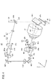
- FIG. 3 is a perspective view showing a specific internal configuration of one of six drawing units shown in FIG. 2.
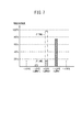
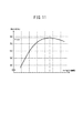
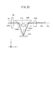
- FIG. 7 is a graph schematically showing the intensity ratio of each diffracted light (including 0th-order light) from the selection optical element (AOM) shown in FIG. 6. It is a figure which shows the schematic structure of the beam switching part for selectively distributing the beam from a light source device to six drawing units, a drawing control apparatus, and a light quantity measurement part. It is a figure explaining the specific internal structure of the light source device shown in FIG.
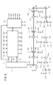
- FIG. FIG. 8 is a block diagram showing a schematic configuration of a beam intensity adjustment control unit that is provided in the drawing control apparatus shown in FIG. 7 and includes a drive circuit that drives each of a plurality of optical elements for selection (AOM) in the beam switching unit. is there. It is a graph which shows an example of the change characteristic of the diffraction efficiency with respect to the change of RF electric power of the drive signal applied to a selection optical element (AOM). It is a block diagram which shows the specific circuit structure of the light quantity measurement part shown in FIG.
- FIG. 9 is a time chart showing an example of the operation of the drawing unit when drawing a pattern for an electronic device based on drawing data (SDn) stored in the drawing control apparatus shown in FIG. 8.
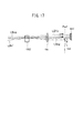
- FIG. 15A shows an optical arrangement according to the second embodiment of the beam switching section shown in FIGS. 2 and 5, and the first stage (upstream side) selection optical element and the next stage (downstream side) selection optical element.
- FIG. 15B is a diagram illustrating an optical arrangement according to the second embodiment of the beam switching unit illustrated in FIGS. 2 and 5 and illustrating an optical path after the selection optical element in the next stage.
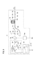
- 15A and 15B are circuit block diagrams illustrating a configuration of a light amount measurement unit for measuring a variation or the like of a selection optical element in the beam switching unit according to the second embodiment of FIGS. 15A and 15B.
- FIG. 15B It is a figure which shows the optical structure by the modification of 2nd Embodiment shown to FIG. 15B. It is a perspective view which shows the optical structure of the beam switching part by 3rd Embodiment, and demonstrates the behavior of each beam generate
- FIG. 1 It is a perspective view which shows the structure of the local temperature control (air cooling) mechanism of the optical element for selection (AOM) provided in the beam switching part shown in FIG. It is a figure which shows the optical structure at the time of using the electro-optic element which switches polarization
- FIG. 1 is a perspective view of the overall configuration of a roll-to-roll substrate processing apparatus (pattern exposure apparatus) as seen from the front side.
- a pattern for an electronic device is referred to as a sheet substrate P (hereinafter also simply referred to as a substrate P) in an exposure unit body (exposure apparatus, drawing apparatus) EX surrounded by a chamber CB.
- a photosensitive layer photosensitive functional layer
- FIG. 1 illustrates exposed to a photosensitive layer (photosensitive functional layer) such as a resist layer, a photosensitive silane coupling layer, or a film of an ultraviolet curable resin.
- a plane parallel to the floor of a factory where the entire substrate processing apparatus is installed is defined as an XY plane of the orthogonal coordinate system XYZ, and a Z direction perpendicular to the XY plane is defined as a gravity direction.
- a long flexible sheet substrate P coated with a photosensitive layer and prebaked (preheated) is mounted on a rotating shaft protruding in the ⁇ Y direction from the supply roll mounting portion EPC1 while being wound around the supply roll FR.
- the supply roll mounting portion EPC1 is provided on the side surface on the ⁇ X side of the unwinding / winding portion 10, and is configured to be finely movable in the ⁇ Y directions as a whole.
- the sheet substrate P drawn from the supply roll FR includes an edge sensor Eps1 attached to a side surface parallel to the XZ plane of the unwinding / winding unit 10, a plurality of rollers having a rotation axis parallel to the Y axis, and a tension. It is sent to a cleaning roller CUR1 attached to the cleaner unit 11 adjacent in the + X direction via a tension roller RT1 that performs application and tension measurement.
- the cleaning roller CUR1 is processed so that the outer peripheral surface has adhesiveness, and rotates in contact with each of the front and back surfaces of the sheet substrate P, thereby removing particles and foreign matters attached to the front and back surfaces of the sheet substrate P. It consists of two rollers to be removed.
- the sheet substrate P that has passed through the cleaning roller CUR1 of the cleaner unit 11 passes through the nip roller NR1 provided to protrude in the ⁇ Y direction from the XZ surface of the tension adjusting unit 12, and the chamber CB of the exposure unit main body EX via the tension roller RT2. Is carried into the exposure unit main body EX through an opening CP1 formed to extend in the Y direction in a slot shape on the side wall of the exposure unit.
- the surface of the sheet substrate P on which the photosensitive layer is formed is upward (+ Z direction) when passing through the opening CP1.
- the sheet substrate P subjected to the exposure processing in the exposure unit main body EX is carried out through the opening CP2 formed in the slot direction in the Y direction on the ⁇ Z side of the opening CP1 and on the side wall of the chamber CB.
- the sheet substrate P carried out through the opening CP2 is disposed adjacent to the ⁇ X direction via a tension roller RT3 and a nip roller NR2 provided to protrude in the ⁇ Y direction from the XZ surface of the tension adjusting unit 12.
- the cleaning roller CUR2 is configured similarly to the cleaning roller CUR1.
- the sheet substrate P that has passed the cleaning roller CUR2 of the cleaner unit 11 is parallel to the tension roller RT4, the edge sensor Eps2, and the Y axis that are attached to the lower step of the side surface parallel to the XZ plane of the unwinding / winding unit 10. It is wound up by the collection roll RR through a plurality of rollers having a rotating shaft.
- the collection roll RR is provided at the lower part of the side surface on the ⁇ X side of the unwinding / winding unit 10 and is mounted on the rotation shaft of the collection roll mounting unit EPC2 configured to be finely movable in the ⁇ Y direction as a whole.
- the collection roll RR winds up the sheet substrate P so that the photosensitive layer of the sheet substrate P faces the outer peripheral surface.
- the width direction (the short direction perpendicular to the long direction) of the surface (surface to be processed) of the sheet substrate P until it is pulled out from the supply roll FR and wound up by the collection roll RR. ) Is always conveyed in the longitudinal direction with the Y direction being in the Y direction.
- the supply roll FR and the recovery roll RR are arranged side by side in the Z direction in the unwinding / winding unit 10, the work of exchanging rolls is simplified.
- a single substrate processing apparatus is configured to perform an exposure process on the sheet substrate P by a roll-to-roll method, but an application unit and a drying unit that apply a photosensitive layer to the surface of the sheet substrate P are provided.
- the wet processing unit and the drying unit that are provided between the supply roll FR and the exposure unit main body EX or perform wet processing such as development processing and plating processing on the sheet substrate P after the exposure processing are collected with the exposure unit main body EX. It may be provided between the rolls RR.
- Each of the supply roll mounting part EPC1 and the recovery roll mounting part EPC2 has a rotation shaft for mounting a roll on which a protective sheet for protecting the surface to be processed of the sheet substrate P is wound. It is installed in parallel with the rotation axis of the collection roll RR.
- the supply roll mounting unit EPC1 includes a servo motor and a gear box (decelerator) that applies a predetermined rotational torque to the supply roll FR, and the servo motor is based on a tension amount measured by the tension roller RT1. Servo controlled by the control unit.
- the collection roll mounting unit EPC2 includes a servo motor and a gear box (decelerator) that applies a predetermined rotational torque to the collection roll RR, and the servo motor is transported based on the tension amount measured by the tension roller RT4. Servo controlled by the control unit of the mechanism.
- the measurement information from the edge sensor Eps1 that measures the displacement in the Y direction of one end portion (edge portion) of the sheet substrate P is the servo that moves the supply roll mounting portion EPC1 (and the supply roll FR) in the ⁇ Y direction.
- the positional deviation in the Y direction of the sheet substrate P that is sent to the motor drive control unit and passes through the edge sensor Eps1 toward the exposure unit main body EX is always kept within a predetermined allowable range.
- the measurement information from the edge sensor Eps2 that measures the displacement in the Y direction of one end portion (edge portion) of the sheet substrate P moves the recovery roll mounting portion EPC2 (and the recovery roll RR) in the ⁇ Y direction. Uneven winding of the sheet substrate P is suppressed by moving the collection roll RR in the Y direction according to the positional deviation in the Y direction of the sheet substrate P passing through the edge sensor Eps2 and sent to the drive control unit of the servo motor.
- a step unit that extends in the X direction and is installed on the factory floor. 13 is provided.
- the step portion 13 has a width of several tens of centimeters in the Y direction so that an operator can go up and perform adjustment work and maintenance work. Further, in the step portion 13, incidental facilities such as various electric wirings, piping for air-conditioning gas, piping for cooling liquid, and the like are accommodated.
- a power source unit 14 On the ⁇ Y direction side of the step portion 13, a power source unit 14, a laser control unit 15 that controls a laser light source that generates an exposure beam, a laser light source, a polygon mirror for pattern drawing, and an optical for beam switching.
- a chiller unit 16 that circulates a coolant (coolant) for cooling a heat generating unit such as a modulator, an air conditioning unit 17 that supplies a temperature-controlled gas into the chamber CB of the exposure unit main body EX, and the like are arranged. .
- the nip roller NR1 and the tension roller RT2 attached to the tension adjusting unit 12 apply a substantially constant tension in the longitudinal direction (conveying direction) to the sheet substrate P on the upstream side of the exposure unit main body EX.
- the tension roller RT2 includes a tension measuring unit (sensor), and can be moved in the ⁇ Z direction in FIG. 1 by a servo motor so that the measured tension amount becomes a commanded value.
- the nip roller NR1 opposes two parallel rollers with a constant pressing force, and sandwiches the sheet substrate P between them while rotating one of the rollers with a servo motor so that the upstream side and the downstream side of the nip roller NR1.
- the tension applied to the sheet substrate P can be divided.
- the conveyance speed of the sheet substrate P can be actively controlled by rotationally driving one of the nip rollers NR1 by a servo motor. For example, if the servo motor of the nip roller NR1 is servo-locked to a stopped state (zero speed), The sheet substrate P can be locked (moored) at the position of the nip roller NR1.
- the nip roller NR2 and the tension roller RT3 attached to the tension adjusting unit 12 apply a substantially constant tension in the longitudinal direction (conveying direction) to the sheet substrate P on the downstream side of the exposure unit main body EX.
- the tension roller RT3 includes a tension measuring unit (sensor), and can be moved in the ⁇ Z direction in FIG. 1 by a servo motor so that the measured tension amount becomes a commanded value. Since the nip roller NR2 is actively controlled by a servo motor in the same manner as the nip roller NR1, the tension applied to the sheet substrate P can be divided between the upstream side and the downstream side of the nip roller NR2. By servo-locking the rotation of the servo motor of the nip roller NR2 to a stop state (zero speed), the sheet substrate P is locked (moored) at the position of the nip roller NR2.
- the supply roll FR is controlled by synchronously controlling the servo motor that rotationally drives the supply roll FR and the servo motor that rotationally drives the nip roller NR1 according to the amount of tension measured by the tension roller RT1.
- a predetermined tension is applied to the sheet substrate P in the conveyance path from the nip roller NR1 to the nip roller NR1.
- the servo motor that rotationally drives the collection roll RR and the servo motor that rotationally drives the nip roller NR2 are synchronously controlled according to the amount of tension measured by the tension roller RT4, so that the nip roller NR2 and the recovery roll RR A predetermined tension is applied to the sheet substrate P in the transport path up to.
- the various rollers of the supply roll FR and the recovery roll RR, the unwinding / winding unit 10, the cleaner unit 11, and the tension adjusting unit 12 shown in FIG. 1 pass the sheet substrate P along the conveyance path (passing through).
- a cantilever type roller (roll) is provided.
- the parallelism between various rollers can be stabilized by using a double-supported roller (roll). Can be maintained.
- FIG. 2 The orthogonal coordinate system XYZ in FIG. 2 is set to be the same as the coordinate system XYZ in FIG. Therefore, unless otherwise specified, the Z direction of the orthogonal coordinate system XYZ will be described as the gravity direction.
- the pattern drawing apparatus EX is used in a device manufacturing system for manufacturing an electronic device by performing an exposure process on a flexible sheet substrate P (hereinafter also simply referred to as a substrate P).
- the device manufacturing system is a manufacturing system in which a manufacturing line for manufacturing, for example, a flexible display as an electronic device, a film-like touch panel, a film-like color filter for a liquid crystal display panel, flexible wiring, or a flexible sensor is constructed.
- Examples of flexible electronic devices include display panels such as organic EL displays and liquid crystal displays, wearable sensor sheets, and the like.
- the sheet substrate P for example, a resin film or a foil (foil) made of a metal or alloy such as stainless steel is used.
- the material of the resin film examples include polyethylene resin, polypropylene resin, polyester resin, ethylene vinyl copolymer resin, polyvinyl chloride resin, cellulose resin, polyamide resin, polyimide resin, polycarbonate resin, polystyrene resin, and vinyl acetate resin. Among them, one containing at least one or more may be used. Further, the thickness and rigidity (Young's modulus) of the sheet substrate P are such that folds due to buckling and irreversible wrinkles do not occur in the sheet substrate P when passing through the conveyance path of the device manufacturing system or the pattern drawing apparatus EX. As long as it is within the range. As the base material of the sheet substrate P, a film such as PET (polyethylene terephthalate) or PEN (polyethylene naphthalate) having a thickness of about 25 ⁇ m to 200 ⁇ m is used.
- PET polyethylene terephthalate
- PEN polyethylene naphthalate
- the sheet substrate P may receive heat in each process performed in the device manufacturing system, it is preferable to select a material that does not have a significantly large thermal expansion coefficient.
- the thermal expansion coefficient can be suppressed by mixing an inorganic filler with a resin film.
- the inorganic filler may be, for example, titanium oxide, zinc oxide, alumina, or silicon oxide.
- the sheet substrate P may be a single-layer body of ultrathin glass having a thickness of about 100 ⁇ m manufactured by a float process or the like, or a laminate in which the above resin film or foil is bonded to the ultrathin glass. It may be a body.
- a film having a thickness of several hundred ⁇ m or less (hereinafter also referred to as a CNF sheet substrate) containing cellulose nanofiber (CNF) can withstand high temperature (for example, about 200 ° C.) treatment compared to a film such as PET, By increasing the content of CNF, the coefficient of linear thermal expansion can be reduced to about copper or aluminum. Therefore, the CNF sheet substrate is formed by forming a wiring pattern of copper to mount electronic components (semiconductor elements, resistors, capacitors, etc.) or directly forming a thin film transistor (TFT) that requires high temperature processing. It is also suitable as a substrate for manufacturing flexible electronic devices. In particular, when an electronic device is manufactured, a dry heat treatment is necessary after the wet treatment. In this case, since the heat resistance is high and the stretchability is low, a long sheet substrate is continuously added to a plurality of sheets. It becomes easy to construct a roll-to-roll manufacturing line that passes through the processing equipment, and an improvement in productivity can be expected.
- the flexibility of the sheet substrate P means that the sheet substrate P can be bent without being sheared or broken even if a force of about its own weight is applied to the sheet substrate P.
- flexibility includes a property of bending by a force of about its own weight.
- the degree of flexibility varies depending on the material, size and thickness of the sheet substrate P, the layer structure formed on the substrate P, the environment such as temperature or humidity, and the like. In any case, when the sheet substrate P is correctly wound around the conveyance direction changing members such as various conveyance rollers and rotating drums provided in the conveyance path in the device manufacturing system (pattern drawing apparatus EX), the sheet substrate P is buckled.
- the sheet substrate P can be smoothly conveyed without creases or breakage (breaking or cracking), it can be said to be in a flexible range.
- a photosensitive functional layer photosensitive layer is formed on the surface of the sheet substrate P by the process of the previous process.
- the photosensitive functional layer is applied as a solution on the substrate P and dried to form a layer (film).
- a typical photosensitive functional layer is a photoresist (in liquid or dry film form), but as a material that does not require development processing, the photosensitivity of the part that has been irradiated with ultraviolet rays is modified.
- SAM silane coupling agent
- a photosensitive reducing agent When a photosensitive silane coupling agent is used as the photosensitive functional layer, the pattern portion exposed to ultraviolet rays on the sheet substrate P is modified from lyophobic to lyophilic.
- a thin film transistor or the like can be formed by selectively applying a conductive ink (ink containing conductive nanoparticles such as silver or copper) or a liquid containing a semiconductor material on the lyophilic portion.
- a pattern layer to be an electrode, a semiconductor, insulation, or a wiring for connection can be formed.
- the photosensitive functional layer may be any other layer, for example, a layer coated with an ultraviolet curable resin, as long as it has sensitivity in the ultraviolet wavelength region (about 250 to 400 nm).
- the plating reducing group is exposed to the pattern portion exposed to the ultraviolet rays on the sheet substrate P. Therefore, after exposure, a pattern layer made of palladium is formed (deposited) by immediately immersing the sheet substrate P in an electroless plating solution containing palladium ions and the like for a certain period of time.
- a plating process is an additive process, but may be based on an etching process as a subtractive process.
- the sheet substrate P sent to the pattern drawing apparatus EX has PET or PEN as a base material, and a metal thin film such as aluminum (Al) or copper (Cu) is entirely or selectively deposited on the surface thereof. It is preferable that a photoresist layer is laminated thereon.
- the pattern drawing apparatus EX conveys the sheet substrate P, which has been conveyed from the previous process apparatus, toward the subsequent process apparatus (including a single processing unit or a plurality of processing units) at a predetermined speed, An exposure process (pattern drawing) is performed on the sheet substrate P.
- the pattern drawing apparatus EX has a pattern for an electronic device (for example, a wiring pattern constituting the electronic device, a pattern of a TFT electrode or wiring, etc.) on the surface of the sheet substrate P (the surface of the photosensitive functional layer, that is, the photosensitive surface). ). Thereby, a latent image (modified portion) corresponding to the pattern is formed on the photosensitive functional layer.
- the pattern drawing apparatus EX in the present embodiment is a direct drawing type exposure apparatus that does not use a mask, that is, a so-called spot scanning type exposure apparatus (drawing apparatus).
- the drawing apparatus EX performs pattern exposure for each part of the rotary drum DR that supports the substrate P and conveys it in the longitudinal direction for sub-scanning, and the substrate P that is supported by the rotary drum DR in a cylindrical surface shape.
- six drawing units Un U1 to U6) are provided, and each of the plurality of drawing units Un (U1 to U6) has a pulsed beam LB for exposure emitted from the light source device LS (pulse beam).
- Spot light is scanned one-dimensionally (main scanning) with a polygon mirror (scanning member) PM in a predetermined scanning direction (Y direction) on the irradiated surface (photosensitive surface) of the substrate P, and the intensity of the spot light Is modulated (ON / OFF) at a high speed in accordance with pattern data (drawing data, pattern information).
- pattern data drawing data, pattern information
- the spot light is relatively two-dimensionally scanned on the irradiated surface of the substrate P (the surface of the photosensitive functional layer), and the irradiated surface of the substrate P A predetermined pattern is drawn and exposed. Since the substrate P is transported at a speed commanded in the longitudinal direction by the rotation of the rotary drum DR, the exposure area where the pattern is drawn by the drawing apparatus EX is predetermined along the longitudinal direction of the substrate P. A plurality of them are provided with an interval of. Since an electronic device is formed in this exposed region, the exposed region is also a device forming region.
- the rotary drum DR has a central axis AXo extending in the Y direction and extending in a direction intersecting with the direction in which gravity works, and a cylindrical outer peripheral surface having a constant radius from the central axis AXo.
- a shaft is provided coaxially with the central axis AXo at both ends in the Y direction of the rotary drum DR, and the rotary drum DR is pivotally supported by a support member (main body frame portion) in the drawing apparatus EX via a bearing. .
- the shaft is coupled coaxially with the rotational axis of the motor 30 (see FIG. 3 below).
- the rotating drum DR rotates around the central axis AXo while supporting (wrapping) a part of the substrate P by bending the outer peripheral surface (circumferential surface) into a cylindrical surface in the longitudinal direction.
- the substrate P is transported in the longitudinal direction.
- the rotary drum DR has a region on the substrate P (a portion including the drawing lines SL1 to SL6 by the spot light) on which the scanning beam (spot light) from each of the plurality of drawing units Un (U1 to U6) is projected. Support on the surface.
- the rotating drum DR supports (holds and holds) the substrate P from the surface (back surface) opposite to the surface on which the electronic device is formed (surface on which the photosensitive surface is formed).
- the light source device (pulse light source device) LS generates and emits a pulsed beam (pulse beam, pulse light, laser) LB.
- This beam LB is ultraviolet light having sensitivity to the photosensitive layer of the sheet substrate P and having a peak wavelength in the ultraviolet wavelength band of about 240 to 400 nm.
- the light source device LS emits a beam LB that emits pulses at a frequency (oscillation frequency, predetermined frequency) Fa in accordance with control of a drawing control device 200 (not shown) (see FIG. 3 later).
- the light source device LS includes a semiconductor laser element that generates pulsed light in the infrared wavelength region, a fiber amplifier, and a wavelength conversion element that converts the amplified pulsed light in the infrared wavelength region into pulsed light having an ultraviolet wavelength of 355 nm ( It is assumed that the fiber amplifier laser light source is composed of a harmonic generation element. By configuring the light source device LS in this manner, high-intensity ultraviolet pulsed light having an oscillation frequency Fa of several hundred MHz and a light emission time of one pulse of several tens of picoseconds or less can be obtained. It is assumed that the beam LB emitted from the light source device LS is a thin parallel light beam having a beam diameter of about 1 mm or less.
- the light source device LS is a fiber amplifier laser light source and the pulse generation of the beam LB is turned on / off at high speed according to the state of the pixels constituting the drawing data (logical value “0” or “1”).
- the state of the pixels constituting the drawing data logical value “0” or “1”.
- the beam LB emitted from the light source device LS is a selection optical element (selection optical member) OSn (OS1 to OS6) as a plurality of switching elements, a plurality of reflection mirrors M1 to M12, and a plurality of selection mirrors IMn ( IM1 to IM6) and a beam switching unit including an absorber TR and the like, and selectively (alternatively) supplied to each of the drawing units Un (U1 to U6).
- the selection optical element OSn (OS1 to OS6) is transmissive to the beam LB, is driven by an ultrasonic signal (RF power), and is the first-order diffracted light (main diffracted beam) of the incident beam LB.
- Is composed of an acousto-optic modulator (AOM: Acousto-Optic Modulator) that deflects and emits the beam as a drawing beam LBn at a predetermined angle.
- AOM Acousto-Optic Modulator
- the plurality of selection optical elements OSn and the plurality of selection mirrors IMn are provided corresponding to each of the plurality of drawing units Un.
- the selection optical element OS1 and the selection mirror IM1 are provided corresponding to the drawing unit U1
- the selection optical elements OS2 to OS6 and the selection mirror IM2 to IM6 correspond to the drawing units U2 to U6, respectively. Is provided.
- the light beam LB from the light source device LS is bent in a spiral shape in a plane parallel to the XY plane by the reflecting mirrors M1 to M12, and the optical elements for selection OS5, OS6, OS3, OS4, OS1, OS2 are sequentially arranged.
- the light is transmitted and guided to the absorber TR.
- the selection optical elements OSn OS1 to OS6
- OS1 to OS6 are in an off state (a state where no ultrasonic signal is applied and no first-order diffracted light is generated)
- a plurality of lenses are provided in the beam optical path from the reflection mirror M1 to the absorber TR, and the plurality of lenses converge the beam LB from the parallel light flux.
- the beam LB that diverges after convergence is returned to a parallel light flux.
- the configuration will be described later with reference to FIG.
- the beam LB from the light source device LS travels in the ⁇ X direction parallel to the X axis and enters the reflection mirror M1.
- the beam LB reflected in the ⁇ Y direction by the reflection mirror M1 enters the reflection mirror M2.
- the beam LB reflected in the + X direction by the reflection mirror M2 passes through the selection optical element OS5 linearly and reaches the reflection mirror M3.
- the beam LB reflected in the ⁇ Y direction by the reflection mirror M3 enters the reflection mirror M4.
- the beam LB reflected in the ⁇ X direction by the reflection mirror M4 is linearly transmitted through the selection optical element OS6 and reaches the reflection mirror M5.
- the beam LB reflected in the ⁇ Y direction by the reflection mirror M5 enters the reflection mirror M6.
- the beam LB reflected in the + X direction by the reflection mirror M6 is linearly transmitted through the selection optical element OS3 and reaches the reflection mirror M7.
- the beam LB reflected in the ⁇ Y direction by the reflection mirror M7 enters the reflection mirror M8.
- the beam LB reflected in the ⁇ X direction by the reflection mirror M8 is linearly transmitted through the selection optical element OS4 and reaches the reflection mirror M9.
- the beam LB reflected in the ⁇ Y direction by the reflection mirror M9 enters the reflection mirror M10.
- the beam LB reflected in the + X direction by the reflection mirror M10 is linearly transmitted through the selection optical element OS1 and reaches the reflection mirror M11.
- the beam LB reflected in the ⁇ Y direction by the reflection mirror M11 enters the reflection mirror M12.
- the beam LB reflected in the ⁇ X direction by the reflection mirror M12 is linearly transmitted through the selection optical element OS2 and guided to the absorber TR.
- the absorber TR detects that the high-intensity beam LB from the light source device LS that is transmitted without being attenuated leaks to the outside when the optical elements for selection OSn (OS1 to OS6) are all off. It is an optical trap to prevent.
- the first-order diffracted light (main diffraction) is obtained by diffracting the incident beam (0th-order light) LB at a diffraction angle corresponding to the frequency of the high frequency. Beam) is generated as an exit beam (drawing beam LBn). Therefore, the beam emitted as the first-order diffracted light from the selection optical element OS1 becomes LB1, and similarly, the beams emitted as the first-order diffracted light from the selection optical elements OS2 to OS6 become LB2 to LB6.
- each of the selection optical elements OSn has a function of deflecting the optical path of the beam LB from the light source device LS.
- the selection optical element OSn (OS1 to OS6) is turned on to generate the beam LBn (LB1 to LB6) as the first-order diffracted light.
- OS1 to OS6 deflect (or select) the beam LB from the light source device LS.
- the maximum generation efficiency of the first-order diffracted light is about 70 to 80% of the zero-order light, so that the beams LBn (LB1 to LB6) deflected by each of the selection optical elements OSn Is lower than the intensity of the original beam LB.
- the drawing control apparatus 200 see FIG. 3) so that only one selected optical element OSn (OS1 to OS6) for selection is turned on (deflection state) for a predetermined time. ).
- OSn is in the ON state, about 20% of 0th order light (0th order diffracted beam) that travels straight without being diffracted by the selected optical element OSn remains. Absorbed by the absorber TR.
- Each of the selection optical elements OSn is installed so as to deflect the drawing beam LBn (LB1 to LB6), which is the deflected first-order diffracted light, in the ⁇ Z direction with respect to the incident beam LB.
- the beams LBn (LB1 to LB6) deflected by each of the selection optical elements OSn are projected onto selection mirrors IMn (IM1 to IM6) provided at positions separated from the selection optical elements OSn by a predetermined distance. .
- Each selection mirror IMn reflects the incident beam LBn (LB1 to LB6) in the ⁇ Z direction, thereby guiding the beam LBn (LB1 to LB6) to the corresponding drawing unit Un (U1 to U6).
- each selection optical element OSn is diffracted light (beam LBn) obtained by diffracting the incident beam LB in accordance with on / off of a drive signal (ultrasonic signal) from the drawing control apparatus 200 (see FIG. 3) Turn on / off the occurrence of
- the selection optical element OS5 transmits the incident beam LB from the light source device LS without being deflected (diffracted) when the drive signal (high-frequency signal) is not applied and is turned off. Therefore, the beam LB transmitted through the selection optical element OS5 enters the reflection mirror M3.
- the selection optical element OS5 when the selection optical element OS5 is in the on state, the incident beam LB is deflected (diffracted) and directed to the selection mirror IM5. That is, the switching (beam selection) operation by the selection optical element OS5 is controlled by turning on / off the drive signal. In this way, the switching operation of each selection optical element OSn can guide the beam LB from the light source device LS to any one drawing unit Un, and switch the drawing unit Un on which the beam LBn is incident. Can do. As described above, the plurality of selection optical elements OSn are arranged in series so that the beams LB from the light source device LS pass in order, and the beams LBn are supplied to the corresponding drawing units Un in a time division manner. Is disclosed in International Publication No. 2015/166910.
- each of the selection optical elements OSn (OS1 to OS6) constituting the beam switching unit is turned on for a predetermined time is, for example, OS1 ⁇ OS2 ⁇ OS3 ⁇ OS4 ⁇ OS5 ⁇ OS6 ⁇ OS1 ⁇ .
- This order is determined by the order of the scanning start timing by the spot light set in each of the drawing units Un (U1 to U6). That is, in the present embodiment, any of the drawing units U1 to U6 is synchronized with the rotation speed of the polygon mirror PM provided in each of the six drawing units U1 to U6 in synchronization with the rotation angle phase. It is possible to switch to time division so that one reflecting surface of one polygon mirror performs spot scanning once on the substrate P.
- the order of spot scanning of the drawing unit Un may be any.
- three drawing units U1, U3, U5 are arranged in the Y direction on the upstream side in the transport direction of the substrate P (the direction in which the outer peripheral surface of the rotary drum DR moves in the circumferential direction).
- Three drawing units U2, U4, U6 are arranged in the Y direction on the downstream side in the transport direction.
- pattern drawing on the substrate P is started from the upstream odd-numbered drawing units U1, U3, U5, and when the substrate P is fed for a certain length, the even-numbered drawing units U2, U4, U6 on the downstream side. Since pattern drawing is also started, the order of spot scanning of the drawing unit Un can be set as U1 ⁇ U3 ⁇ U5 ⁇ U2 ⁇ U4 ⁇ U6 ⁇ U1 ⁇ . Therefore, the order in which each of the selection optical elements OSn (OS1 to OS6) is turned on for a predetermined time is determined as OS1 ⁇ OS3 ⁇ OS5 ⁇ OS2 ⁇ OS4 ⁇ OS6 ⁇ OS1 ⁇ .
- the on / off switching control of the selection optical element OSn is based on the drawing data. By doing so, the selection optical element OSn is forcibly maintained in the OFF state, so that spot scanning by the drawing unit Un is not performed.
- each of the drawing units U1 to U6 is provided with a polygon mirror PM for main scanning the incident beams LB1 to LB6.
- the polygon mirrors PM of the respective drawing units Un are synchronously controlled so as to maintain a constant rotational angle phase with each other while precisely rotating at the same rotational speed.
- the main scanning timing (main scanning period of the spot light SP) of each of the beams LB1 to LB6 projected onto the substrate P from each of the drawing units U1 to U6 can be set so as not to overlap each other.
- each of the selection optical elements OSn (OS1 to OS6) provided in the beam switching unit is controlled in synchronization with the rotation angle positions of the six polygon mirrors PM, thereby providing a light source.
- An efficient exposure process can be performed in which the beam LB from the apparatus LS is distributed in time division to each of the plurality of drawing units Un.
- the drawing apparatus EX is a so-called multi-head type direct drawing exposure apparatus in which a plurality of drawing units Un (U1 to U6) having the same configuration are arranged.
- Each of the drawing units Un draws a pattern for each partial region partitioned in the Y direction of the substrate P supported by the outer peripheral surface (circumferential surface) of the rotary drum DR.
- Each drawing unit Un (U1 to U6) condenses (converges) the beam LBn on the substrate P while projecting the beam LBn from the beam switching unit onto the substrate P (on the irradiated surface of the substrate P). Thereby, the beam LBn (LB1 to LB6) projected onto the substrate P becomes spot light.
- the spot light of the beam LBn (LB1 to LB6) projected on the substrate P is scanned in the main scanning direction (Y direction) by the rotation of the polygon mirror PM of each drawing unit Un.
- the drawing line SLn is also a scanning locus of the spot light of the beam LBn on the substrate P.
- the drawing unit U1 scans the spot light along the drawing line SL1, and similarly, the drawing units U2 to U6 scan the spot light along the drawing lines SL2 to SL6.
- the drawing lines SLn (SL1 to SL6) of the plurality of drawing units Un (U1 to U6) rotate around a central plane pcc that includes the central axis AXo of the rotary drum DR and is parallel to the YZ plane. Arranged in a staggered arrangement in two rows in the circumferential direction of the drum DR.
- the odd-numbered drawing lines SL1, SL3, SL5 are located on the irradiated surface of the substrate P on the upstream side ( ⁇ X direction side) in the transport direction of the substrate P with respect to the center plane pcc, and along the Y direction. Are arranged in a row at a predetermined interval.
- the even-numbered drawing lines SL2, SL4, SL6 are located on the irradiated surface of the substrate P on the downstream side (+ X direction side) in the transport direction of the substrate P with respect to the center surface, and are predetermined along the Y direction. Are arranged in a row separated by an interval of.
- the plurality of drawing units Un (U1 to U6) are also arranged in a staggered arrangement in two rows in the transport direction of the substrate P across the center plane pcc, and odd-numbered drawing units U1, U3, U5 and even-numbered drawing units
- the drawing units U2, U4, and U6 are provided symmetrically with respect to the center plane pcc when viewed in the XZ plane.
- the odd-numbered drawing lines SL1, SL3, SL5 and the even-numbered drawing lines SL2, SL4, SL6 are separated from each other, but the Y direction ( With respect to the width direction of the substrate P and the main scanning direction), they are set to be joined together without being separated from each other.
- the drawing lines SL1 to SL6 are substantially parallel to the width direction of the substrate P, that is, the central axis AXo of the rotary drum DR.
- splicing the drawing line SLn in the Y direction means that the end of the drawing line SLn is such that the pattern drawn in each of the drawing lines SLn adjacent in the Y direction is spliced in the Y direction on the substrate P. This means that the positions in the Y direction are adjacent or partially overlapped.
- the length of each drawing line SLn may be overlapped within a range of several percent or less in the Y direction including the drawing start point or the drawing end point. .
- the plurality of drawing units Un share the Y-direction scanning area (the main scanning range section) so as to cover the width dimension of the exposure area on the substrate P in total. ing.
- the main scanning range in the Y direction the length of the drawing line SLn
- drawing can be performed by arranging a total of six drawing units U1 to U6 in the Y direction.
- the width in the Y direction of a large exposure area (pattern formation area) can be increased to about 180 to 360 mm.
- the length of each drawing line SLn (SL1 to SL6) (length of the drawing range) is basically the same. That is, the scanning distance of the spot light of the beam LBn scanned along each of the drawing lines SL1 to SL6 is basically the same.
- the beam LB from the light source device LS is pulsed light having a light emission time of several tens of picoseconds or less (1/10 or less with respect to the period Tf of the oscillation frequency Fa).
- the spot light projected onto the drawing line SLn is discrete according to the oscillation frequency Fa (for example, 400 MHz) of the beam LB. Therefore, it is necessary to overlap the spot light projected by one pulse light of the beam LB and the spot light projected by the next one pulse light in the main scanning direction.
- the amount of the overlap is set by the effective size ⁇ of the spot light, the spot light scanning speed (main scanning speed) Vs, and the oscillation frequency Fa of the beam LB.
- the effective size (diameter) ⁇ of the spot light is 1 / e 2 (or half the full width at half maximum) of the peak intensity of the spot light SP when the intensity distribution of the spot light SP is approximated by a Gaussian distribution. It is determined by the width dimension.
- the spot light scanning speed Vs rotation speed of the polygon mirror PM
- oscillation so that the spot light overlaps with an effective size (dimension) ⁇ of about ⁇ ⁇ 1 ⁇ 2.
- the frequency Fa is set. Therefore, the projection interval of the pulsed spot light along the main scanning direction is ⁇ / 2.
- the substrate P has an effective size of the spot light between one scanning of the spot light along the drawing line SLn and the next scanning. It is desirable to set so as to move by a distance approximately half of ⁇ . Further, when drawing lines SLn adjacent in the Y direction are continued in the main scanning direction, it is desirable to overlap by ⁇ / 2.
- the effective size (dimension) ⁇ of the spot light on the substrate P is set to 2 to 4 ⁇ m, which is about the same as the size of one pixel set on the drawing data.
- Each drawing unit Un (U1 to U6) is set so that each beam LBn travels toward the central axis AXo of the rotary drum DR when viewed in the XZ plane.
- the optical path (beam principal ray) of the beam LBn traveling from each drawing unit Un (U1 to U6) toward the substrate P becomes parallel to the normal line of the irradiated surface of the substrate P in the XZ plane.
- the beam LBn irradiated from each of the drawing units Un (U1 to U6) to the drawing line SLn (SL1 to SL6) is relative to the tangential plane at the drawing line SLn on the surface of the substrate P curved into a cylindrical surface. It is projected toward the substrate P so as to be always vertical. That is, with respect to the main scanning direction of the spot light, the beams LBn (LB1 to LB6) projected onto the substrate P are scanned in a telecentric state.
- the drawing unit U1 includes at least reflecting mirrors M20 to M24, a polygon mirror PM, and an f ⁇ lens system (drawing scanning lens) FT.
- a first cylindrical lens CYa (see FIG. 4) is disposed in front of the polygon mirror PM when viewed from the traveling direction of the beam LB1, and an f ⁇ lens system (f- ⁇ lens system) is provided.
- a second cylindrical lens CYb (see FIG. 4) is provided after the FT.
- the first cylindrical lens CYa and the second cylindrical lens CYb correct the positional variation in the sub-scanning direction of the spot light (drawing line SL1) due to the tilt error of each reflecting surface RP of the polygon mirror PM.
- the beam LB1 reflected in the ⁇ Z direction by the selection mirror IM1 enters the reflection mirror M20 provided in the drawing unit U1, and the beam LB1 reflected by the reflection mirror M20 advances in the ⁇ X direction and enters the reflection mirror M21.
- the beam LB1 reflected in the ⁇ Z direction by the reflection mirror M21 enters the reflection mirror M22, and the beam LB1 reflected by the reflection mirror M22 advances in the + X direction and enters the reflection mirror M23.
- the reflection mirror M23 bends the beam LB1 in a plane parallel to the XY plane so that the incident beam LB1 is directed to the reflection surface RP of the polygon mirror PM.
- the polygon mirror PM reflects the incident beam LB1 toward the + ⁇ direction toward the f ⁇ lens system FT.
- the polygon mirror PM deflects (reflects) the incident beam LB1 in a one-dimensional manner in a plane parallel to the XY plane in order to scan the spot light of the beam LB1 on the irradiated surface of the substrate P.
- the polygon mirror (rotating polygonal mirror, scanning member) PM includes a rotation axis AXp extending in the Z-axis direction, and a plurality of reflecting surfaces RP (mainly formed around the rotation axis AXp and in parallel with the rotation axis AXp). In the embodiment, the number Np of the reflecting surfaces RP is 8).
- the reflection angle of the pulsed beam LB1 irradiated on the reflection surface can be continuously changed by rotating the polygon mirror PM around the rotation axis AXp in a predetermined rotation direction.
- the beam LB1 is deflected by one reflecting surface RP, and the spot light of the beam LB1 irradiated on the irradiated surface of the substrate P is scanned along the main scanning direction (width direction of the substrate P, Y direction). be able to.
- the number of scans of the spot light along the drawing line SL1 on the irradiated surface of the substrate P by one rotation of the polygon mirror PM is eight, which is the same as the number of the reflection surfaces RP.
- the number of times the spot light is scanned on the irradiated surface of the substrate P by one rotation of the polygon mirror PM is four.
- the f ⁇ lens system (scanning lens, scanning optical system) FT is a telecentric scanning lens that projects the beam LB1 reflected by the polygon mirror PM onto the reflecting mirror M24.
- the beam LB1 transmitted through the f ⁇ lens system FT is condensed on the substrate P as spot light through the reflection mirror M24 (and the second cylindrical lens CYb described in FIG. 4).
- the reflection mirror M24 reflects the beam LB1 toward the substrate P so that the beam LB1 travels toward the central axis AXo of the rotary drum DR with respect to the XZ plane.
- the incident angle ⁇ of the beam LB1 to the f ⁇ lens system FT (the deviation angle from the optical axis of the f ⁇ lens system FT) changes according to the rotation angle ( ⁇ / 2) of the polygon mirror PM.
- the f ⁇ lens system FT projects the beam LB1 to the image height position on the irradiated surface of the substrate P in proportion to the incident angle ⁇ through the reflection mirror M24.
- the focal length of the f ⁇ lens system FT is fo and the image height position is yo
- the beam LB1 can be scanned in the Y direction accurately at a constant speed by the f ⁇ lens system FT.
- the surface (parallel to the XY plane) on which the beam LB1 incident on the f ⁇ lens system FT is deflected one-dimensionally by the polygon mirror PM is a surface including the optical axis of the f ⁇ lens system FT.
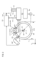
- FIG. 3 schematically shows an encoder measurement system that measures the rotational angle position of the rotary drum DR shown in FIG. 2 and a mark detection system (alignment system) that detects the position of the alignment mark pattern formed on the substrate P.
- a mark detection system alignment system
- FIG. 3 the rotating drum DR is provided with a shaft Sft extending in the Y direction coaxially with the central axis AXo, and the shaft Sft is coupled coaxially with the rotating shaft of the motor 30.
- a disk-like or annular scale member ESD is fixed to the end of the rotary drum DR in the Y direction, coaxially with the shaft Sft (center axis AXo), and rotates in the XZ plane together with the rotary drum DR.
- On the outer peripheral surface parallel to the central axis AXo of the scale member ESD a grid-like scale is engraved at a constant pitch (for example, about 20 ⁇ m) along the circumferential direction.
- the diameter of the scale member ESD is shown smaller than the diameter of the outer peripheral surface of the rotating drum DR, but the radius from the central axis AXo of the scale member ESD is ⁇ 5% with respect to the radius of the outer peripheral surface of the rotating drum. It is better to keep them within a certain range.
- a plane parallel to the YZ plane including the central axis AXo is the central plane pcc.
- the beams LB1, LB3, and LB5 projected from the odd-numbered drawing units U1, U3, and U5 are inclined by an angle + ⁇ u with respect to the center plane pcc. Is set as follows.
- the angle ⁇ u is set to about 10 ° to 20 °.
- An alignment system AMS is provided for detecting the position of the reference mark formed on the surface.
- the objective lens OBL of the alignment system AMS has a detection visual field (detection area) of about 200 to 500 ⁇ m square on the substrate P, and the alignment system AMS is a CCD or CMOS that captures an image of a mark appearing in the detection area at a high shutter speed.
- the imaging device is provided.
- An image signal including the image of the mark imaged (captured) by the image sensor is subjected to image analysis by the alignment measurement system 500, and the relative position between the center position of the imaged mark image and the reference position (center point) in the detection region.
- Information on the amount of misalignment in two dimensions (main scanning direction and sub-scanning direction) is generated.
- the extension line of the optical axis of the objective lens OBL is arranged so as to intersect the central axis AXo of the rotary drum DR within a predetermined error range.
- the encoder head EH1 is set to have the same orientation as the detection area of the objective lens OBL when viewed from the central axis AXo
- the encoder head EH2 is an odd-numbered beam LB1 (LB3) when viewed from the central axis AXo.
- Each of the encoder heads EH1, EH2, and EH3 outputs a two-phase signal that periodically changes in level according to the movement of the scale member ESD in the circumferential direction and has a phase difference of 90 degrees to the counter circuit unit 502.
- the counter circuit unit 502 Based on the two-phase signal from the encoder head EH1, the counter circuit unit 502 provides the alignment measurement system 500 with a measurement value CV1 obtained by digitally counting the amount of movement (position change) of the scale with a resolution of submicron (eg, 0.2 ⁇ m) Output.
- the alignment measurement system 500 latches and stores the measurement value CV1 at the moment when the image pickup device of the alignment system AMS captures the image of the mark in the detection region, and the relative displacement of the mark image obtained by image analysis.
- the position information Dam Based on the amount and the latched measurement value CV1, the position information Dam calculated by associating the position of the mark on the substrate P with the rotation angle position (measurement value CV1) of the rotary drum DR with submicron accuracy is drawn. Output to the control device 200.
- the counter circuit unit 502 digitally counts the moving amount (position change) of the scale with a resolution of submicron (for example, 0.2 ⁇ m) based on the two-phase signals from the encoder heads EH2 and EH3.
- CV2 and CV3 are output to the drawing control apparatus 200.
- the drawing control apparatus 200 controls the drawing position (timing) in the sub-scanning direction by the odd-numbered drawing units U1, U3, U5 based on the measurement value CV2, and the even-numbered drawing unit U2 based on the measurement value CV3.
- U4, and U6 control the drawing position (timing) in the sub-scanning direction.
- a drive circuit unit 504 that precisely servo-controls the rotational speed of the motor 30 based on at least one of the measured values CV1 to CV3 counted by the counter circuit unit 502 or at least two average values is provided.
- the counter circuit unit 502 inherent errors in the encoder measurement system (eccentric error of the scale member ESD, roundness error, scale pitch error, etc.) are measured in advance over the entire circumference of the scale member ESD.
- a correction map for correction is stored, and the measurement values CV1, CV2, and CV3 are output to the alignment measurement system 500 and the drawing control apparatus 200 in a state corrected in real time by the correction map.
- the optical configuration of the drawing unit Un (U1 to U6) will be described with reference to FIG. 4, but the configuration of the drawing unit U1 will be described here as a representative.
- the reflection mirror M20, the reflection mirror M20a, and the polarization beam splitter BS1 are arranged along the traveling direction of the beam LB1 from the incident position of the beam LB1 to the irradiated surface (substrate P).
- the reflection mirror M21, the reflection mirror M22, the first cylindrical lens CYa, the reflection mirror M23, the polygon mirror PM, the f ⁇ lens system FT, the reflection mirror M24, and the second cylindrical lens CYb are provided in the unit frame. It is done.
- the unit frame is configured to be detached from the apparatus main body.
- a beam expander system BE including two lenses Be1 and Be2 is provided in the optical path of the beam LB1 reflected in the ⁇ X direction by the reflection mirror M20 and directed to the reflection mirror M20a.
- This beam expander system BE converts the cross-sectional diameter of the incident beam LB1 (diameter is 1 mm or less) into a parallel light beam expanded to about several mm (8 mm as an example).
- the beam LB1 expanded by the beam expander system BE is reflected in the ⁇ Y direction by the reflection mirror M20a and then enters the polarization beam splitter BS1.
- the beam LB1 is set to linearly polarized light that is efficiently reflected in the ⁇ X direction by the polarization beam splitter BS1.
- the beam LB1 reflected by the polarization beam splitter BS1 is transmitted to a peripheral portion (for example, 1 / e of the base) on the intensity profile of the beam LB1 by a diaphragm FAP having a circular aperture disposed between the reflection mirror M21 and the reflection mirror M22. 2 or less strength part) is cut.
- the beam LB1 reflected in the + X direction by the reflection mirror M22 is converted into circularly polarized light by the quarter-wave plate QW, and then enters the first cylindrical lens CYa.
- an origin sensor that detects the angular position of each reflecting surface RP of the polygon mirror PM in order to detect the drawing start possible timing (spot light scanning start timing) of the drawing unit U1.
- a beam transmitting system 60a and a beam receiving system 60b are provided.
- the reflected light of the beam LB1 reflected by the irradiated surface of the substrate P (or the surface of the rotating drum DR) is converted into the f ⁇ lens system FT, the polygon mirror PM, the polarization beam splitter BS1, and the like.
- a lens system G10 and a photodetector (photoelectric sensor) DTo are provided.
- the beam LB1 incident on the drawing unit U1 advances in the ⁇ Z direction along the axis AX1 parallel to the Z axis, and enters the reflection mirror M20 inclined by 45 ° with respect to the XY plane.
- the beam LB1 reflected by the reflection mirror M20 travels from the reflection mirror M20 through the beam expander system BE toward the reflection mirror M20a separated in the ⁇ X direction.
- the reflection mirror M20a is disposed with an inclination of 45 ° with respect to the YZ plane, and reflects the incident beam LBn toward the polarization beam splitter BS1 in the ⁇ Y direction.
- the polarization separation surface of the polarization beam splitter BS1 is disposed at an angle of 45 ° with respect to the YZ plane, reflects a P-polarized beam, and transmits a linearly polarized (S-polarized) beam polarized in a direction orthogonal to the P-polarized light.
- the polarization beam splitter BS1 reflects the beam LB1 from the reflection mirror M20a in the ⁇ X direction and guides it to the reflection mirror M21 side.
- the reflection mirror M21 is disposed at an angle of 45 ° with respect to the XY plane, and reflects the incident beam LB1 from the reflection mirror M21 via the stop FAP toward the reflection mirror M22 separated in the ⁇ Z direction in the ⁇ Z direction.
- the reflection mirror M22 is disposed at an angle of 45 ° with respect to the XY plane, and reflects the incident beam LB1 in the + X direction toward the reflection mirror M23.
- the beam LB1 reflected by the reflection mirror M22 enters the reflection mirror M23 via the ⁇ / 4 wavelength plate QW and the first cylindrical lens CYA.
- the reflection mirror M23 reflects the incident beam LB1 toward the polygon mirror PM.
- the polygon mirror PM reflects the incident beam LB1 toward the + X direction toward an f ⁇ lens system FT having an optical axis AXf parallel to the X axis.
- the polygon mirror PM deflects (reflects) the incident beam LB1 one-dimensionally in a plane parallel to the XY plane in order to scan the spot light SP of the beam LB1 on the irradiated surface of the substrate P.
- the polygon mirror PM has a plurality of reflecting surfaces (each side of a regular octagon in this embodiment) formed around a rotation axis AXp extending in the Z-axis direction, and is rotated by a rotation motor RM coaxial with the rotation axis AXp. Is done.
- the rotation motor RM rotates at a constant rotation speed (for example, about 30,000 to 40,000 rpm) by a polygon rotation control unit provided in the drawing control apparatus 200 (FIG. 3).
- the effective length (for example, 50 mm) of the drawing lines SLn is the maximum scanning length (for example, 52 mm) at which the spot light SP can be scanned by the polygon mirror PM.
- the length is set as follows, and in the initial setting (design), the center point of the drawing line SLn (the point through which the optical axis AXf of the f ⁇ lens system FT passes) is set at the center of the maximum scanning length.
- the first cylindrical lens CYa converges the incident beam LB1 on the reflection surface of the polygon mirror PM in the sub-scanning direction (Z direction) orthogonal to the main scanning direction (rotation direction) of the polygon mirror PM. That is, the cylindrical lens CYa converges the beam LB1 in a slit shape (ellipse shape) extending in a direction parallel to the XY plane on the reflection surface of the polygon mirror PM.
- the incident angle ⁇ of the beam LBn to the f ⁇ lens system FT (the angle with respect to the optical axis AXf) varies depending on the rotation angle ( ⁇ / 2) of the polygon mirror PM.
- the incident angle ⁇ of the beam LBn to the f ⁇ lens system FT is 0 degree
- the beam LBn incident on the f ⁇ lens system FT advances along the optical axis AXf.
- the beam LBn from the f ⁇ lens system FT is reflected in the ⁇ Z direction by the reflecting mirror M24, and is projected toward the substrate P through the cylindrical lens CYb.
- the beam LB1 projected on the substrate P is about several ⁇ m in diameter on the irradiated surface of the substrate P by the action of the f ⁇ lens system FT, the cylindrical lens CYb whose generating line is parallel to the Y direction, and the beam expander system BE.
- the light is converged to a small spot light SP of 2 to 3 ⁇ m.
- the beam LB1 incident on the drawing unit U1 is bent along the optical path cranked in a U-shape from the reflection mirror M20 to the substrate P when viewed in the XZ plane, and proceeds in the ⁇ Z direction to the substrate. Projected to P.
- the axis AX1 shown in FIG. 4 is an extension of the center line of the beam LB1 incident on the reflection mirror M20.
- This axis AX1 is the light of the f ⁇ lens system FT bent in the ⁇ Z direction by the reflection mirror M24. It arrange
- the entire drawing unit U1 (reflection mirror M20 to second cylindrical lens CYb) can be slightly rotated around the axis AX1, and a slight inclination of the drawing line SL1 in the XY plane can be achieved. Can be adjusted with high accuracy.
- the configuration of the drawing unit U1 is the same for each of the other drawing units U2 to U6.
- each of the six drawing units U1 to U6 scans the spot lights SP of the beams LB1 to LB6 one-dimensionally in the main scanning direction (Y direction), while transporting the substrate P in the longitudinal direction,
- the irradiated surface of the substrate P is relatively two-dimensionally scanned by the spot light SP, and the pattern drawn on each of the drawing lines SL1 to SL6 is exposed on the substrate P in a state where the patterns are joined in the Y direction.
- the effective scanning length LT of the drawing lines SLn is 50 mm
- the effective diameter ⁇ of the spot light SP is 4 ⁇ m
- the oscillation frequency Fa of the pulse emission of the beam LB from the light source device LS is 400 MHz.
- the pulsed light is emitted so that the spot light SP overlaps by 1/2 of the diameter ⁇ along the drawing line SLn (main scanning direction)
- the pixel size Pxy defined on the drawing data is set to 4 ⁇ m square on the substrate P, and one pixel is exposed by two pulses of the spot light SP in each of the main scanning direction and the sub-scanning direction.
- the rotation speed VR may be set to 36000 rpm.
- the scanning speed Vsp (0.8 ⁇ m / nS) is 2880 Km / h in terms of speed.
- two pulses of the beam LBn are overlapped by 1 ⁇ 2 of the diameter ⁇ of the spot light SP in each of the main scanning direction and the sub-scanning direction to form one pixel.
- one pulse corresponds to 3 pulses that are overlapped by 2/3 of the diameter ⁇ of the spot light SP, or 4 pulses that are overlapped by 3/4 of the diameter ⁇ of the spot light SP. You may set to do. Accordingly, if the number of pulses of the spot light SP per pixel is Nsp, the relational expression of Expression 2 can be generalized as Expression 3 below.
- Equation 3 Parameters that can be easily adjusted to satisfy the relationship of Equation 3 are the oscillation frequency Fa (period Tf) of the light source device LS and the rotational speed VR of the polygon mirror PM.
- the rotation angle position of the reflection surface RP of the polygon mirror PM can start scanning of the spot light SP of the drawing beam LBn by the reflection surface RP.
- An origin signal also referred to as a synchronization signal or timing signal
- SZn whose waveform changes is generated at the moment immediately before reaching a predetermined position (specified angle position, origin angle position). Since the polygon mirror PM has eight reflecting surfaces RP, the beam receiving system 60b outputs eight origin signals SZn (eight waveform changes) during one rotation of the polygon mirror PM.
- the origin signal SZn is sent to the drawing control apparatus 200, and after the origin signal SZn is generated, drawing of the spot light SP along the drawing line SLn is started after a predetermined delay time has elapsed.
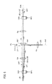
- FIG. 5 is a diagram showing a specific configuration around the optical element for selection OSn (OS1 to OS6) and the selection mirror IMn (IM1 to IM6), but is shown in FIG. 2 for simplicity of explanation.
- a configuration around the selection optical element OS2 that finally receives the beam LB from the light source device LS and the selection optical element OS1 immediately before that is shown as a representative.
- a beam LB emitted from the light source device LS is incident on the selection optical element OS1 as a parallel light beam having a minute diameter (first diameter) having a diameter of 1 mm or less, for example, so as to satisfy the Bragg diffraction condition.
- the incident beam LB is transmitted without being diffracted by the selection optical element OS1.
- the transmitted beam LB passes through the condensing lens Ga and the collimating lens Gb provided on the optical path along the optical axis AXa, and is incident on the subsequent selection optical element OS2.
- the beam LB passing through the condensing lens Ga and the collimating lens Gb through the selection optical element OS1 is coaxial with the optical axis AXa.
- the condensing lens Ga condenses the beam LB (parallel light beam) transmitted through the selection optical element OS1 so as to be a beam waist at the position of the surface Ps located between the condensing lens Ga and the collimating lens Gb. .
- the collimating lens Gb turns the beam LB diverging from the position of the surface Ps into a parallel light beam.
- the diameter of the beam LB converted into a parallel light beam by the collimating lens Gb is the first diameter.
- the condensing lens Ga and the collimating lens Gb are hereinafter simply referred to as lenses (lens members) Ga and Gb or lenses (lens members) Ga and Gb.
- a lens-laminated lens may also be used.
- the rear focal position of the condenser lens Ga and the front focal position of the collimator lens Gb coincide with the surface Ps within a predetermined allowable range
- the front focal position of the condenser lens Ga is the optical element for selection.
- the diffractive point in OS1 is arranged so as to coincide with a predetermined allowable range
- the rear focal position of the collimating lens Gb is arranged so as to coincide with the diffractive point in the selection optical element OS2 within a predetermined allowable range.
- the condensing lens Ga and the collimating lens Gb optically conjugate the diffraction point (beam deflection region) in the selection optical element OS1 and the diffraction point (beam deflection region) in the selection optical element OS2. Functions as a 1 ⁇ magnification optical system (inverted imaging system). Therefore, the pupil plane of the Lerry optical system (lenses Ga and Gb) is formed at the position of the plane Ps.
- the beam LB incident on the Bragg diffraction condition is a beam LB1 (first-order diffracted light, main diffraction beam) diffracted by the selection optical element OS1.
- a zero-order beam LB1z that has not been diffracted.
- a negative first-order diffracted beam (LB1 ′) and other second-order diffracted beams hardly occur in theory. Therefore, when the Bragg diffraction condition is satisfied, when the intensity of the incident beam LB is 100% and the decrease due to the transmittance of the optical element for selection OS1 is ignored, the intensity of the diffracted beam LB1 is 70 to 80 at maximum. The remaining 30 to 20% is the intensity of the zero-order beam LB1z.
- the 0th-order beam LB1z passes through the relay optical system including the condensing lens Ga and the collimating lens Gb, and further passes through the selection optical element OS2 in the subsequent stage and is absorbed by the absorber TR.
- the beam LB1 (parallel light beam) deflected in the ⁇ Z direction at a diffraction angle corresponding to the frequency of the high-frequency drive signal DF1 passes through the condenser lens Ga and travels toward the selection mirror IM1 provided on the surface Ps. Since the front focal position of the condensing lens Ga is optically conjugate with the diffraction point in the selection optical element OS1, the beam LB1 directed from the condensing lens Ga to the selection mirror IM1 has a position decentered from the optical axis AXa. The light travels parallel to the axis AXa and is focused (converged) so as to be a beam waist at the position of the surface Ps. The position of the beam waist is set so as to be optically conjugate with the spot light SP projected onto the substrate P via the drawing unit U1.
- the beam LB1 deflected (diffracted) by the selection optical element OS1 is reflected in the ⁇ Z direction by the selection mirror IM1, and collimated lens ( The light enters the drawing unit U1 along the axis AX1 (see FIG. 4) via the lens and lens member) Gc.
- the collimating lens Gc turns the beam LB1 converged / diverged by the condenser lens Ga into a parallel light beam coaxial with the optical axis (axis line AX1) of the collimating lens Gc.
- the diameter of the beam LB1 converted into a parallel light beam by the collimating lens Gc is substantially the same as the first diameter.
- the rear focal point of the condensing lens Ga and the front focal point of the collimating lens Gc are arranged on or near the reflecting surface of the selection mirror IM1 within a predetermined tolerance.
- the front focal position of the condenser lens Ga and the diffraction point in the selection optical element OS1 are optically conjugated, and the selection mirror IM1 is disposed on the surface Ps that is the rear focal position of the condenser lens Ga. Then, the beam LB1 (main diffracted beam) diffracted by the selection optical element OS1 can be surely selected (switched) at a position where the beam waist becomes.
- a relay optical system (inverted imaging system) of the same magnification composed of a similar condenser lens Ga and collimator lens Gb is also provided between OS1 and OS1.
- a ⁇ 1st order diffracted beam LB1 ′ that is not theoretically generated is generated as leakage light.
- the ⁇ 1st order diffracted beam LB1 ′ (parallel light beam) is generated at a diffraction angle (deflection angle) symmetrical to the main diffracted beam LB1 with respect to the 0th order beam LB1z in the selection optical element OS1, and is incident on the condenser lens Ga.
- the beam waist converges on the surface Ps.
- the condensing point of the ⁇ 1st order diffracted beam LB1 ′ is located symmetrically with the condensing point of the main diffracted beam LB1 across the condensing point of the 0th order beam LB1z. Since the selection mirror IM1 reflects only the main diffracted beam LB1, the other 0th-order beam LB1z and ⁇ 1st-order diffracted beam LB1 ′ enter the collimating lens Gb as they are, and are in the off-stage selection optics. The light enters the element OS2.
- the ⁇ 1st-order diffracted beam LB1 ′ passes through the selection optical element OS2 as it is, and the incident angle (exit angle) at that time is the diffraction angle (deflection angle) when the selection optical element OS2 is turned on. ). Therefore, the ⁇ 1st-order diffracted beam LB1 ′ (leakage light and stray light) that has passed through the selection optical element OS2 is converged by the condenser lens Ga at the rear stage of the selection optical element OS2 and reflected by the selection mirror IM2 at the rear stage. Then, the light enters the drawing unit U2.
- the selection optical element OS1 when the selection optical element OS1 is turned on and the drawing unit U1 draws a pattern by scanning with the spot light SP, the ⁇ 1st order diffracted beam LB1 ′ (sub-diffraction beam) modulated with the same drawing data is simultaneously produced.
- the light enters the drawing unit U2.
- one of the reflection surfaces of the polygon mirror PM of the drawing unit U2 has an angle range in which the ⁇ 1st order diffracted beam LB1 ′ (sub-diffraction beam) as incident noise light is reflected toward the f ⁇ lens system FT. If so, the spot light SP is scanned so as to draw a pattern (noise pattern) different from the original pattern on the drawing line SL2.
- the intensity (light quantity) of the ⁇ 1st order diffracted beam LB1 ′ is lower than the intensity of the original beam LB2 (+ 1st order diffracted beam) scanned by the drawing unit U2, it is extraneous to the photosensitive layer on the sheet substrate P.
- the exposure amount is given, that is, the exposure state with the noise pattern is applied, and the quality of the pattern finally drawn on the sheet substrate P is greatly deteriorated.
- the polygon mirror PM that prevents noise light ( ⁇ 1st-order diffracted beam LB1 ′) incident on the drawing unit U2 from entering the f ⁇ lens system FT of the drawing unit U2.
- the noise light reflected by the reflection surface of the polygon mirror PM can be applied to other members in the drawing unit U2, the lens barrel (metal) of the f ⁇ lens system FT, etc. Therefore, scattered light or the like generated therefrom may enter the f ⁇ lens system FT as stray light. Therefore, in the present embodiment, as shown in FIG. 5, the ⁇ 1st order diffracted beam LB1 ′ (sub-diffraction beam that becomes noise light) generated by the selecting optical element OS1 is incident on the selecting optical element OS2 at the subsequent stage. In order to prevent this, a reflection mirror IM1 ′ as a blocking optical member is disposed at the position of the surface Ps.
- the reflection mirror IM1 ' is disposed by rotating the same mirror as the selection mirror IM1 by 180 ° around the optical axis AXa (0th-order beam LB1z beam).
- the reflection mirror IM1 ′ shields the ⁇ 1st-order diffracted beam LB1 ′, which has become a beam waist at the position of the surface Ps, so as not to enter the selection optical element OS2 at the subsequent stage, and prevents exposure due to noise patterns.
- the light blocking member (knife edge) may be used as the blocking optical member.
- the light-shielding member does not substantially shield the ⁇ 1st-order diffracted beam LB1 ′, so that the -1st-order diffracted beam LB1 is not substantially affected, for example, about 1/100 to 1/1000. It may be one that attenuates the intensity of '.
- the reflection mirror IM1 ′ is provided to not only shield (block) the ⁇ 1st-order diffracted beam LB1 ′ (noise light) but also branch it from the optical path of the relay optical system (lenses Ga and Gb).
- the -1st order diffracted beam LB1 ′ (noise light) is photoelectrically detected by reflecting the light toward the photoelectric sensor DT1. Since the photoelectric signal Sm1 output from the photoelectric sensor DT1 corresponds to the intensity change of the ⁇ 1st-order diffracted beam LB1 ′ (noise light), it is possible to monitor the fluctuation (such as fluctuation of diffraction efficiency) of the selection optical element OS1.
- the ⁇ 1st order diffracted beams LB1 ′ to LB6 ′ generated as noise light from the selection optical elements OS1 to OS6 are collectively referred to as LBn ′, reflecting mirrors IM1 ′ to IM6 ′ (second deflecting member).
- IMn ′ the photoelectric sensors DT1 to DT6
- DTn photoelectric signals Sm1 to Sm6 from each of the photoelectric sensors DTn.
- the selection optical element OSn is bonded to a crystal (or quartz) AOG for diffracting the incident beam LB and one side of the crystal AOG, and is supplied with RF power (drive signal DFn).
- An ultrasonic transducer VD for generating a periodic refractive index distribution (transmission type phase diffraction grating) in the crystal AOG.
- An axis perpendicular to the periodic direction of the grating is Lga.
- the angle ⁇ B which is a condition for Bragg diffraction, is also called a Bragg angle. Therefore, the crystal body AOG is formed so that the incident surface Pin and the exit surface Pout are parallel to each other, and not perpendicular to the axis Lga but perpendicular to the beam LB incident at the Bragg angle ⁇ B. As a result, the beam LB transmitted through the selection optical element OSn or the 0th-order beam LBnz travels straight without being laterally shifted by the crystal AOG.
- the ideal Bragg is affected by the temperature change of the crystal AOG, the frequency change of the RF power (drive signal DFn), the slight change from the Bragg angle ⁇ B of the incident beam LB, the change of the environmental temperature and the atmospheric pressure, etc. If the diffraction condition is not met, a ⁇ 1st order diffracted beam LBn ′ (sub-diffraction beam) as noise light is generated.
- the ⁇ 1st order diffracted beam LBn ′ is generated at a diffraction angle ⁇ d that is symmetrical to the diffraction angle + ⁇ d of the main diffracted beam LBn with respect to the 0th order beam LBnz.
- FIG. 7 is a graph showing an example of intensity distribution of diffracted light (including zero-order light) emitted from the optical element for selection OSn (crystal AOG), and the vertical axis represents the incident beam LB as 1 (100%).
- a second-order or higher diffraction beam is not generated.
- the + 1st order diffracted beam LBn and the ⁇ 1st order diffracted beam LBn ′ are not generated, and only the 0th order beam LBnz has a high ratio, for example, the incident beam It is generated at a ratio (for example, about 98%) obtained by multiplying the intensity of LB by the transmittance ⁇ of the optical element for selection OSn (crystal AOG).
- the + 1st order diffracted beam LBn is generated with an efficiency ⁇ corresponding to the magnitude of the RF power (amplitude of the drive signal DFn).
- the efficiency ⁇ is about 80% at the maximum, and the intensity of the + 1st order diffracted beam LBn considering the transmittance ⁇ is about 78% at the maximum with respect to the intensity of the beam LB. Accordingly, the intensity of the 0th-order diffracted beam LBnz that has not been diffracted in the ON state is about 20%.
- the ratio of the intensities of the + 1st-order diffracted beam LBn and the 0th-order diffracted beam LBnz decreases from the ideal state (catalog value). .
- the present embodiment while preventing (shielding) the propagation of the ⁇ 1st-order diffracted beam LBn ′ (sub-diffraction beam) to the subsequent drawing unit Un generated as noise light by the blocking optical member (reflection mirror IM1 ′),
- the variation of the diffraction efficiency ⁇ of the optical element for selection OSn is monitored by detecting the intensity of the ⁇ 1st order diffracted beam LBn ′ with the photoelectric sensor DTn shown in FIG. 5, and the beam finally projected on the sheet substrate P
- the intensity fluctuation of LBn (+ 1st order diffracted beam) can be specified. Therefore, an error from the appropriate exposure amount of the pattern drawn on the substrate P can be estimated and corrected.
- FIG. 8 shows a beam switching unit (selection optical elements OS1 to OS6, reflection mirrors M1 to M12, selection mirror) that selectively supplies the beam LB from the light source device LS shown in FIG. 2 to each of the drawing units U1 to U6.
- 1 shows a schematic arrangement of the light source device LS, the drawing control device (drawing control unit) 200, and the light amount measurement unit 202.
- the drawing control apparatus (drawing control unit) 200 inputs the origin signals SZ1 to SZ6 from the beam receiving systems 60b of the drawing units U1 to U6 shown in FIG. 4, and sets the pattern drawing timing of each drawing unit Un. At the same time, the drive signals DF1 to DF6 whose amplitude is adjusted (power adjustment) are output to each of the selection optical elements OS1 to OS6. As described with reference to FIG. 2, the beam LB from the light source device LS is reflected by the reflection mirrors M1 and M2 and sequentially passes through the optical elements for selection OS5, OS6, OS3, OS4, OS1, and OS2, and then FIG.
- the reflection mirror M13 reflects the 0th-order diffracted beam that has not been reflected by the selection mirror IM2 through the selection optical element OS2 toward the absorber TR.
- the reflection mirrors M1 to M13 and the selection mirrors IM1 to IM6 included in the beam switching unit are laser mirrors similar to the reflection mirrors M20 to M24 in the drawing unit Un, and have a slight transmittance (for example, 1) at the wavelength 355 nm of the beam LB. % Or less).
- a photoelectric sensor DTa that detects the intensity (light quantity) of the beam LB emitted from the light source device LS is provided on the back surface side of the reflection mirror M1, and all of the photoelectric mirrors D13 are provided on the back surface side of the reflection mirror M13.
- a photoelectric sensor DTb that detects the beam LB that is transmitted when the selection optical elements OS1 to OS6 are in the OFF state or the 0th-order diffraction beam LBnz of the beam LB that has not been diffracted by the selection optical element OSn in the ON state. Provided.
- the photoelectric sensors DTa and DTb are each configured by a PIN photodiode, an avalanche photodiode (APD), or a metal-semiconductor-metal (MSM) photodiode.
- the photoelectric signal Sa output from the photoelectric sensor DTa is sent to the light amount measuring unit 202 to monitor the original intensity (light amount) of the beam LB emitted from the light source device LS, and is output from the photoelectric sensor DTb.
- Sb is sent to the light quantity measuring unit 202 in order to monitor fluctuations in transmittance and diffraction efficiency of the six optical elements for selection OS1 to OS6.
- the ⁇ 1st order diffracted beam LB1 as noise light reflected by each of the reflection mirrors IM1 ′ to IM6 ′ provided symmetrically with each of the selection mirrors IM1 to IM6 with respect to the optical axis AXa. ' ⁇ LB6' is received by the photoelectric sensors DT1 to DT6, respectively. Photoelectric signals Sm1 to Sm6 output from each of the photoelectric sensors DT1 to DT6 are sent to the light quantity measuring unit 202 in order to monitor variations in diffraction efficiency of the selection optical elements OS1 to OS6.
- the photoelectric sensors DT1 to DT6 are configured by any one of a PIN photodiode, an avalanche photodiode (APD), and an MSM photodiode.
- the light source device LS is a fiber amplifier laser light source (laser light source that generates ultraviolet pulsed light using an optical amplifier and a wavelength conversion element) as shown in FIG.
- the configuration of the fiber amplifier laser light source (LS) in FIG. 9 is disclosed in detail, for example, in the pamphlet of International Publication No. 2015/166910, and will be briefly described here.
- the light source device LS has a control circuit 120 including a signal generator 120a that generates a clock signal LTC for causing the beam LB to emit light at a frequency Fa, and pulses in the infrared wavelength region in response to the clock signal LTC.
- a seed light generator 135 that generates two types of seed light S1 and S2 that emit light.
- the seed light generator 135 includes DFB semiconductor laser elements 130 and 132, lenses GLa and GLb, a polarization beam splitter 134, and the like.
- the DFB semiconductor laser element 130 has a peak intensity in response to a clock signal LTC (for example, 400 MHz).
- LTC for example, 400 MHz.
- a large, sharp or sharp pulse-shaped seed light S1 is generated, and the DFB semiconductor laser element 132 generates a pulse-shaped seed light S2 having a small peak intensity and a slow (time broad) response in response to the clock signal LTC. appear.
- the seed light S1 and the seed light S2 are set so that the light emission timings are synchronized (matched) and the energy per one pulse (peak intensity ⁇ light emission time) is substantially the same.
- the polarization state of the seed light S1 generated by the DFB semiconductor laser element 130 is set to S polarization
- the polarization state of the seed light S2 generated by the DFB semiconductor laser element 132 is set to P polarization.
- the polarization beam splitter 134 transmits the S-polarized seed light S 1 from the DFB semiconductor laser element 130 and guides it to the electro-optical element (EO element by Pockels cell, car cell, etc.) 136 and also P-polarized light from the DFB semiconductor laser element 132.
- the seed light S ⁇ b> 2 is reflected and guided to the electro-optical element 136.
- the electro-optic element 136 draws drawing data (drawing bit string data corresponding to the number of pixels drawn during one scan of the spot light SP) sent from the drawing control apparatus 200 in FIG.
- the polarization state of the two types of seed light S1 and S2 is switched at high speed by the drive circuit 136a according to the number corresponding to any of U6).
- the electro-optical element 136 does not change the polarization state of the seed beams S1 and S2, and remains as it is.
- the electro-optic element 136 rotates the polarization direction of the incident seed light S1 and S2 by 90 degrees to obtain a polarization beam splitter. Lead to 138. Therefore, when the logical information of the pixel of the drawing bit string data SDn is in the H state (“1”), the electro-optic element 136 converts the S-polarized seed light S1 into the P-polarized seed light S1, and the P-polarized seed light S1. The light S2 is converted into S-polarized seed light S2.
- the polarization beam splitter 138 transmits P-polarized light and guides it to the combiner 144 via the lens GLc, and reflects S-polarized light to the absorber 140.
- the seed light (one of S1 and S2) that passes through the polarization beam splitter 138 is referred to as a seed light beam Lse.
- Excitation light (pump light, charge light) from the excitation light source 142 guided to the combiner 144 through the optical fiber 142 a is combined with the seed light beam Lse emitted from the polarization beam splitter 138 and enters the fiber optical amplifier 146. To do.
- the seed light beam Lse is amplified while passing through the fiber optical amplifier 146 by exciting the laser medium doped in the fiber optical amplifier 146 with the excitation light.
- the amplified seed light beam Lse is emitted from the exit end 146a of the fiber optical amplifier 146 with a predetermined divergence angle, and enters the first wavelength conversion optical element 148 through the lens GLd.
- the first wavelength conversion optical element 148 generates a second harmonic whose wavelength is 1 ⁇ 2 of ⁇ with respect to the incident seed light beam Lse (wavelength ⁇ ) by second harmonic generation (SHG). Is generated.
- the second harmonic (wavelength ⁇ / 2) of the seed light beam Lse and the original seed light beam Lse (wavelength ⁇ ) are incident on the second wavelength conversion optical element 150 through the lens GLe so as to be condensed. .
- the second wavelength conversion optical element 150 generates a sum frequency (Sum Frequency Generation: SFG) of the second harmonic (wavelength ⁇ / 2) and the seed light beam Lse (wavelength ⁇ ), so that the wavelength is 1/3 of ⁇ .
- the third harmonic is generated.
- the third harmonic becomes ultraviolet pulsed light (beam LB) having a peak wavelength in a wavelength band of 370 mm or less (for example, 355 nm).
- the beam LB (divergent light beam) generated from the second wavelength conversion optical element 150 is converted into a parallel light beam having a beam diameter of about 1 mm by the lens GLe and emitted from the light source device LS.
- the electro-optical element 136 receives the incident seed light S1.
- S2 is directly guided to the polarization beam splitter 138 without changing the polarization state. Therefore, the seed light beam Lse incident on the combiner 144 is derived from the seed light S2. Since the fiber optical amplifier 146 has low peak intensity and low amplification efficiency with respect to the seed light S2 having a dull characteristic that is broad in time, the P-polarized beam LB emitted from the light source device LS is necessary for exposure. It becomes pulse light that is not amplified to a sufficient energy.
- the energy of the beam LB generated from such seed light S2 is extremely low, and the intensity of the spot light SP irradiated on the substrate P is extremely low.
- the beam LB emitted in such a non-drawing state is turned off. Also called a beam (off-pulse light).
- the electro-optical element 136 receives the incident seed light.
- the polarization states of S1 and S2 are changed and guided to the polarization beam splitter 138. Therefore, the seed light beam Lse incident on the combiner 144 is derived from the seed light S1.
- the seed light beam Lse Since the emission profile of the seed light beam Lse derived from the seed light S1 has a large peak intensity and sharpness, the seed light beam Lse is efficiently amplified by the fiber optical amplifier 146, and the P-polarized beam LB output from the light source device LS is It has energy necessary for exposure of the substrate P.
- the beam LB In order to distinguish the beam LB output from the light source device LS in the drawing state from the off beam (off pulse light) emitted in the non-drawing state, the beam LB is also referred to as an on beam (on pulse light). Call.
- the fiber amplifier laser light source can be an ultraviolet pulse light source that emits burst light at high speed in response to drawing data (SDn).
- the clock signal LTC from the signal generation unit 120a in FIG. 9 is also supplied to the drawing control device 200 and the light amount measurement unit 202, as shown in FIG.
- the drawing control apparatus 200 receives the origin signals SZ1 to SZ6 from each of the drawing units U1 to U6, matches the rotation speed of the polygon mirror PM of each of the drawing units U1 to U6, and sets the rotation angle position (rotation).
- the rotation of the polygon mirror PM is synchronously controlled so that the phase of the polygon mirror PM is in a predetermined relationship with each other.
- the light source device LS and the drawing control device 200 exchange various control information (commands and parameters) via an interface bus (which may be a serial bus) SJ connected to the control circuit 120 in the light source device LS.
- the drawing control apparatus 200 includes a memory that stores drawing bit string data SDn to be drawn by the drawing lines SL1 to SL6 by the spot lights SP of the drawing units U1 to U6 based on the origin signals SZ1 to SZ6. Further, in the drawing control apparatus 200, the number of pulses of the beam LB for drawing one pixel of data (1 bit) of the drawing bit string data SDn stored in the memory is set in advance. For example, when one pixel is set to be drawn with two pulses of the beam LB (two spot lights SP in each of the main scanning direction and the sub-scanning direction), the drawing bit string data SDn is 2 of the clock signal TLC. For each clock pulse, one pixel (1 bit) is read and applied to the drive circuit 136a in FIG.
- FIG. 10 is a block diagram illustrating an example of the configuration of the drive module.
- the drive module includes a switch for turning on one of the selection optical elements OS1 to OS6 in response to the origin signals SZ1 to SZ6 from each of the drawing units U1 to U6.
- An intensity adjustment control unit 250 is provided that generates the signals LP1 to LP6 and controls where the intensity (amplitude of the high frequency signal) of each of the drive signals DF1 to DF6 is set within a predetermined adjustable range.
- Each of the six high frequency amplifier circuits 251a to 251f that applies the drive signals DF1 to DF6 to each of the selection optical elements OS1 to OS6 has a high frequency of a certain reference frequency (for example, several tens of MHz to 100 MHz) from the signal source RF.
- the signals are applied in common, and the high-frequency amplifier circuits 251a to 251f switch the drive signals DF1 to DF6 between the state where they are applied to the selection optical elements OS1 to OS6 and the state where they are not applied in response to the switch signals LP1 to LP6, respectively. .
- each of the high frequency amplifier circuits 251a to 251f receives the setting signals Pw1 to Pw6 generated by the gain setting circuits 252a to 252f, and adjusts the strength (amplitude, gain) of each of the drive signals DF1 to DF6.
- the intensity of each of the drive signals DF1 to DF6 to be set is calculated by the CPU in the light quantity measuring unit 202 shown in FIG. 9 or the CPU in the drawing control apparatus 200.
- Information that is the basis of the calculation includes photoelectric signals Sa and Sb from the photoelectric sensors DTa and DTb described in FIG. 8 and photoelectric signals from the photoelectric sensors DT1 to DT6 that receive the noise light ( ⁇ 1st order diffracted beam LBn ′). Signals Sm1 to Sm6.
- the high frequency power (RF power) of the drive signal DFn supplied to each of the selection optical elements (AOM) OSn and the diffraction efficiency ⁇ are an example.
- the horizontal axis represents the RF power (amplitude of the drive signal DFn) input to the AOM
- the vertical axis represents the diffraction efficiency ⁇ (%) of the AOM + first order diffracted beam used in Bragg diffraction.
- the diffraction efficiency ⁇ of the AOM has a characteristic that reaches the maximum diffraction efficiency ⁇ max as the RF power increases, and the diffraction efficiency ⁇ decreases even if the RF power is increased further. Therefore, the adjustment of the diffraction efficiency of each of the selection optical elements OS1 to OS6 (setting of the amplitude of the drive signal DFn) is performed in consideration of the maximum diffraction efficiency ⁇ max.
- the intensity adjustment control unit 250 shown in FIG. 10 is based on the change in the amplitude of the drive signal DFn and the change in the diffraction efficiency ⁇ of the selection optical element OSn (and the change in the diffraction efficiency ⁇ ) based on the characteristics shown in FIG.
- the correlation with the estimated + 1st order diffracted beam LBn intensity change) is obtained in advance and stored in a table or a functional expression.
- the light quantity measurement unit 202 includes amplifier circuits 220a to 220f that amplify the photoelectric signals Sm1 to Sm6 from the photoelectric sensors DT1 to DT6 provided in the subsequent stage of the selection optical elements OS1 to OS6 of the beam switching unit, photoelectric A sample hold (S / H) circuit 222 is selected by selecting any one of amplifier circuits 225a and 225b for amplifying the photoelectric signals Sa and Sb from the sensors DTa and DTb and the amplified photoelectric signals Sm1 to Sm6.
- amplifier circuits 220a to 220f that amplify the photoelectric signals Sm1 to Sm6 from the photoelectric sensors DT1 to DT6 provided in the subsequent stage of the selection optical elements OS1 to OS6 of the beam switching unit
- photoelectric A sample hold (S / H) circuit 222 is selected by selecting any one of amplifier circuits 225a and 225b for amplifying the photoelectric signals Sa and Sb from the sensors DTa and DTb and the amp
- the multiplexer circuit 221 and the amplified photoelectric signals Sa and Sb From the multiplexer circuit 221 and the amplified photoelectric signals Sa and Sb, and the multiplexer circuit 226 and the S / H circuits 222 and 227 which select one of the amplified photoelectric signals Sa and Sb and send it to the sample hold (S / H) circuit 227 Analog / digital conversion (ADC) times to convert the signal level (integral value or peak value) to digital value 223,228, and includes measurement operation, the collection of measurement results, the microprocessor (MPU) 224 which generally controls data communication or the like with the drawing control unit 200.
- ADC Analog / digital conversion
- the processor (MPU) 224 Based on the clock signal LTC generated by the light source device LS, the processor (MPU) 224 sends a control signal CS1 for instructing respective operation timings to the S / H circuits 222 and 227 and the ADC circuits 223 and 228. At the same time, a control signal CS2 for instructing the timing of the selection operation is sent to the multiplexer circuits 221 and 226.
- each drawing unit Un (U1 to U6) draws a pattern for an electronic device based on the drawing data (SDn) stored in the drawing control apparatus 200 of FIG. To do.
- An example of the drawing operation of the drawing unit Un at that time will be briefly described with reference to the time chart of FIG.
- the origin signal SZn from the origin sensor (the beam receiving system 60b in FIG. 4) in the drawing unit Un is, for example, one reflecting surface RPa of the eight reflecting surfaces RP of the polygon mirror PM and the next reflecting surface.
- the origin pulses STZna and SDnb are generated.
- the origin pulses STZna and SDnb are generated at a time interval TPab at which the polygon mirror PM rotates 45 ° corresponding to the rotation speed of the polygon mirror PM.
- the origin signal SZn includes six origin pulses SDnc to SZnh that are generated at a time interval TPab following the origin pulses SDZa and SDnb shown in FIG. 13 during one rotation of the polygon mirror PM.
- the switch signal LPn (LP1 ⁇ LP1) output from the intensity adjustment control unit 250 shown in FIG. As shown in FIG.
- LP6 starts from “L” to turn on the optical element for selection OSn after a predetermined delay time ⁇ Ta has elapsed from the time of generation of one origin pulse SDZa of the origin signal SZn. It switches to “H”, and from “H” to “L” immediately before the elapse of time TPab / 3 from the generation of the origin pulse SDna.
- the switch signals LPn (LP1 to LP6) are switched from “L” to “H” after the delay time ⁇ Tb to ⁇ Th, and each of the origin pulses SZnb to SZnh is changed. It switches from “H” to “L” just before the time TPab / 3 has elapsed since the occurrence.
- one drawing unit Un has a polygon mirror PM.
- the beam LBn is controlled to be scanned every other one of the eight reflecting surfaces RP.
- the switch signal LPn (LP1 to LPn to LPn in response to each of, for example, four origin pulses STZna, SPnzc, SDne, and SDngg that are generated by skipping one of the eight origin pulses SDZa to SDnzh generated in succession. LP6) switches from “L” to “H”, and from “H” to “L” immediately before the elapse of time TPab / 3.
- the spot light SP (beam LBn) modulated in response to the drawing bit string data SDn is 1 along the drawing line SLn. Scanned once.
- the drawing bit string data SDn is applied from the drawing control device 200 to the drive circuit 136a in the light source device LS of FIG. 9 as a bit serial signal representing one pixel by one bit.
- the drawing bit string data SDn and the clock signal LTC from the light source device LS are two clocks of one clock signal LTC by the drawing control device 200. It is controlled to correspond to the pulse.
- the light source device LS when a pixel having 1 bit of “0” is an Off pixel and a hatched “1” pixel is an On pixel, the light source device LS has two pulses of the beam LBn for the Off pixel. Minute (two clock pulses of the clock signal LTC) is output in the state of off-pulse light with extremely low intensity, and for the On pixel, two pulses of the beam LB are output in the state of high-intensity on-pulse light. Output.
- the light amount measurement unit 202 illustrated in FIG. 8 has one selection optical element that is turned on among the six selection optical elements OSn.
- a photoelectric signal Smn from one photoelectric sensor DTn corresponding to OSn is selected by the multiplexer circuit 221, and the intensity of the generated noise light ( ⁇ 1st order diffracted beam LBn ′) is measured and stored. This measurement is performed while the spot light SP is scanned at least once along the drawing line SLn, but during the pattern drawing in a predetermined pattern drawing region (exposed region) on the substrate P.
- the selection optical element OSn that is turned on at that time and generates the beam LBn (+ 1st order diffraction beam) is sequentially identified Then, the intensity of the noise light ( ⁇ 1st order diffracted beam LBn ′) corresponding to each of the selection optical elements OSn (drawing unit Un) is measured.
- the processor (MPU) 224 of the light quantity measurement unit 202 measures in advance in an initial state (a state at the time of calibration) in which the amplitude of each drive signal DFn of the optical element for selection OSn is adjusted so that an appropriate exposure amount can be obtained.
- the measurement result of the intensity of the noise light ( ⁇ 1st order diffracted beam LBn ′) and the intensity measurement result of the noise light ( ⁇ 1st order diffracted beam LBn ′) measured during the pattern drawing operation are compared. If there is a difference exceeding the allowable range, it is estimated that the selection optical element OSn that has generated such a difference has changed for some reason. As described above with reference to the graph of FIG.
- the intensity of the noise light ( ⁇ 1st order diffracted beam LBn ′) has increased is relatively the intensity of the drawing beam LBn (+ 1st order diffracted beam LBn). Means that it has declined. Conversely, if the intensity of the noise light ( ⁇ 1st order diffracted beam LBn ′) decreases, it means that the intensity of the drawing beam LBn (+ 1st order diffracted beam LBn) has increased relatively. Therefore, the processor (MPU) 224 of the light amount measuring unit 202 or the CPU of the drawing control apparatus 200 draws a beam LBn (+ 1st order diffraction) corresponding to the intensity change of the measured noise light ( ⁇ 1st order diffraction beam LBn ′). The intensity change of the beam LBn) is estimated with reference to the relational characteristic between the RF power and the diffraction efficiency ⁇ in FIG.
- the CPU of the drawing control apparatus 200 sends the intensity adjustment control unit 250 shown in FIG.
- a setting signal Pwn that adjusts (increases or decreases) the power (amplitude) of the drive signal DFn for the selection optical element OSn that selects the drawing beam LBn (+ 1st order diffraction beam LBn) to be adjusted
- a setting signal Pwn that adjusts (increases or decreases) the power (amplitude) of the drive signal DFn for the selection optical element OSn that selects the drawing beam LBn (+ 1st order diffraction beam LBn) to be adjusted
- the above measurement operation and adjustment operation are performed at an appropriate timing while the drawing unit Un draws and exposes a certain pattern on the substrate P, for example, at regular time intervals or in a sub-scanning direction. It is performed sequentially every time.
- the light amount measurement unit 202 illustrated in FIG. The intensity of ( ⁇ 1st-order diffracted beam LBn ′) cannot be measured at all, or the reliability of the measured value is significantly reduced.
- the address value of drawing bit string data having a high density that becomes On pixels during one scan, or a sub-column of a pixel string in which many On pixels are arranged in the main scanning direction is specified, and when the address value or the position of the pixel column in the sub-scanning direction is reached, the above measurement operation and adjustment operation may be performed.
- two or more selection optical elements (AOM) OSn are arranged in series along the optical path of the beam LB from the light source device LS, and crystals of these selection optical elements OSn are arranged.
- the relay optical system (lenses Ga, Gb) is provided so that the body (diffraction medium) is optically conjugate with each other, the upstream selection optical element OSn is turned on, and the beam from the light source device LS
- a drawing beam LBn (+ 1st order diffracted beam LBn) by Bragg diffraction of LB a ⁇ 1st order diffracted beam LBn ′ as noise light that can be generated in the upstream selection optical element OSn is
- the light is shielded by a reflection mirror IMn ′ as a light shielding member arranged on the pupil plane in the relay optical system or in the vicinity of the pupil space so as not to enter the selection optical element OSn.
- the 0th-order diffracted beam LBnz directly transmitted through the upstream selection optical element OSn, the diffracted drawing beam LBn (+ 1st-order diffracted beam LBn), and ⁇ 1 as noise light Since each of the second-order diffracted beams LBn ′ becomes a beam waist and is spatially separated and distributed, the unnecessary ⁇ 1st-order diffracted beam LBn ′ can be surely cut. For this reason, the ⁇ 1st-order diffracted beam LBn ′ as noise light is prevented from entering the downstream drawing unit Un through the downstream selection optical element OSn.
- the phenomenon of ghost exposure (cover exposure) in which another pattern is drawn with a low exposure amount is eliminated, and deterioration of drawing quality can be suppressed.
- the intensity (light quantity) change of the drawing beam LBn (+ 1st order diffracted beam LBn) caused by the change in the diffraction efficiency (change from the Bragg diffraction condition) of the selection optical element OSn is automatically performed.
- the ⁇ 1st order diffracted beam LBn ′ which becomes noise light at the time of pattern drawing, can be utilized, and in order to measure the intensity of the beam LBn for drawing (+ 1st order diffracted beam LBn)
- an amplitude division type optical member a reflection mirror having a low transmittance, a glass or quartz plate having a low reflectance
- a wavefront division type optical member a polarization beam splitter, etc.
- FIG. 14 shows a selection mirror IMn that reflects the drawing beam LBn and a ⁇ 1st-order diffracted beam LBn ′ (secondary light) as noise light in the optical arrangement of the beam switching section of the first embodiment shown in FIG. It is a perspective view which shows the modification at the time of integrating with reflective mirror IMn 'which reflects a (diffracted beam).
- the support disk FP having a circular opening FPh formed at the center is made of a light-shielding material such as metal, ceramics, or ultraviolet shielding glass.
- the support disk FP has a pupil space at a position slightly shifted from the position in the direction of the optical axis AXa, assuming that the plane Ps at the substantially center of the relay optical system (lenses Ga and Gb) shown in FIG. Installed.
- the selection mirror IMn and the reflection mirror IMn ′ are fixed to the surface of the support disk FP in a state where the selection mirror IMn and the reflection mirror IMn ′ are rotated 180 ° around the optical axis AXa with the circular opening FPh interposed therebetween.
- the arrangement relationship between the selection mirror IMn and the reflection mirror IMn ′ is that the space between the drawing beam LBn (+ 1st order diffracted beam LBn) with respect to the optical axis AXa of the 0th order diffracted beam LBnz and the ⁇ 1st order diffracted beam LBn ′ as noise light. And positioned on the support disk FP so as to match the general separation state.
- the support disk FP including the selection mirror IMn and the reflection mirror IMn ′ can be finely moved in each of the Z direction, the Y direction, and the X direction in FIG. It is mounted on a part of the body frame to which the element is mounted.
- the position of the support disk FP is finely adjusted so that the drawing beam LBn reflected by the selection mirror IMn is exactly the same as the incident axis AX1 of the beam LB of the drawing unit Un shown in FIG. Is set to be coaxial.
- a photoelectric sensor DTn (see FIG. 5) that receives the ⁇ 1st-order diffracted beam LBn ′ as noise light reflected by the reflection mirror IMn ′ is provided in a portion where the + Z direction of the support disk FP in FIG. 14 is slightly extended. It may be fixed. In the modification shown in FIG.
- the support disk FP is made of a light-shielding material, but may be made of a light-transmitting material that exhibits high transmittance in the wavelength region of the beam LB, such as a quartz plate. In that case, as shown in FIG. 14, it is not necessary to provide the circular opening FPh through which the beam LB and the zero-order diffraction beam LBnz pass.
- [Second Embodiment] 15A and 15B show an optical configuration of the beam switching unit according to the second embodiment.
- the beam switching unit according to the first embodiment optically transmits each of the plurality of selection optical elements OSn arranged so that the beam LB from the light source device LS passes in series.
- a relay optical system an inverted imaging system
- the relay optical system for bringing each of the plurality of selection optical elements OSn into a conjugate relationship (imaging relationship) is changed to an erect image forming system.
- FIG. 15A shows an optical configuration between the selection optical element OS2 at the final stage of the beam switching unit and the selection optical element OS1 immediately before that, corresponding to FIG. Then, a two-time relay optical system (upright imaging system) in which four lenses (lens members) Ga, Gd, Ge, and Gb are arranged between the optical elements for selection OS1 and OS2 along the light transmission path of the beam LB. Is provided.
- the arrangement of the selection optical element OS1, the lens Ga, the selection mirror IM1, and the lens Gc in the on state is the same as the configuration of FIG.
- the selection optical element OS1 When the selection optical element OS1 is in the ON state, the 0th-order diffracted beam LB1z and the ⁇ 1st-order diffracted beam LB1 ′ as noise light are incident on a lens Gd arranged coaxially with the optical axis of the relay optical system.
- the focal lengths of the front side and the rear side of the lens Gd are fd, the surface Ps1 is set at the position of the front focal length Fd of the lens Gd.
- the surface Ps2 at the position of the rear focal length fd of the lens Gd is a surface optically conjugate with the selection optical element OS1 (an inverted imaging surface), and the 0th-order diffracted beam LB1z and the ⁇ 1st-order diffracted beam LB1. 'Intersects as a parallel luminous flux.
- the selection mirror (reflecting member) IM1 is disposed in a pupil space including the surface Ps1 between the lens Ga and the lens Gd.
- the 0th-order diffracted beam LB1z and the -1st-order diffracted beam LB1 'that have passed through the surface Ps2 are incident on the lens Ge having front and rear focal lengths fe.
- the focal length fe of the lens Ge is set equal to the focal length fd of the lens Gd.
- each of the 0th-order diffracted beam LB1z and the ⁇ 1st-order diffracted beam LB1 ′ is in a state parallel to the optical axis and positioned at the rear focal length fe. Is converged to be a beam waist at the surface Ps3.
- the surface Ps3 has an optically conjugate relationship (inverted imaging relationship) with the surface Ps1, and the position of the ⁇ 1st-order diffracted beam LB1 ′ on the surface Ps3 and 0
- the relationship with the position (on the optical axis) of the next diffraction beam LB1z is obtained by rotating the positional relationship on the plane Ps1 by 180 ° around the optical axis.
- the 0th-order diffracted beam LB1z and the ⁇ 1st-order diffracted beam LB1 ′ that have passed through the surface Ps3 are incident on the lens Gb having front and rear focal lengths fb.
- the focal length fb of the lens Gb is set equal to the focal length fa of the lens Ga.
- the surface Ps3 is set at the position of the front focal length fb of the lens Gb and the selection optical element OS2 at the next stage (final stage) is set at the position of the rear focal distance fb, the 0th-order diffraction beam LB1z and the ⁇ 1st-order diffraction are set.
- Each of the beams LB1 ′ becomes a parallel light beam and is incident so as to intersect in the selection optical element OS2 in the next stage.
- the selection optical element OS2 in the next stage Since the selection optical element OS2 in the next stage is in the off state, the 0th-order diffracted beam LB1z and the ⁇ 1st-order diffracted beam LB1 ′ incident on the selection optical element OS2 are transmitted as they are as shown in FIG. Incident at the front and rear focal lengths fa).
- the ⁇ 1st order diffracted beam LB1 ′ as noise light incident on the selection optical element OS2 at the next stage has an angle with respect to the axis (optical axis) of the 0th order diffracted beam LB1z as compared with the case of the configuration of FIG.
- the diffraction direction of the selection optical element OS2 (the pitch direction of the grating) is reversed.
- the ⁇ 1st order diffracted beam LB1 ′ that travels straight through the selection optical element OS2 and is converged by the lens Ga passes through the space on the opposite side of the selection mirror IM2 with respect to the optical axis (0th order diffracted beam LB1z). It becomes the beam waist. Therefore, even when the first-stage selection optical element OS1 is in the ON state, even if the ⁇ 1st-order diffracted beam LB1 ′ as noise light is generated and enters the subsequent-stage selection optical element OS2, it does not enter the selection mirror IM2. It will be.
- the relay optical system for bringing the two selection optical elements OSn arranged one after the other along the optical path of the beam LB from the light source device LS into a conjugate relationship is correct.
- a vertical image forming system that is, by providing two stages of inverted image forming relay optical systems, the ⁇ 1st order diffracted beam LB1 ′ as noise light generated by the selection optical element OSn in the previous stage is provided in the subsequent stage. It is prevented from entering the selection mirror IMn (drawing unit Un).
- the two-time relay optical system (upright imaging system) using lenses Ga, Gd, Ge, and Gb shown in FIG. 15A is between the selection optical elements OS5 and OS6 of the beam switching unit shown in FIG.
- the focal length fa of the lens Ga is equal to the focal length fb of the lens Gb
- the focal length fd of the lens Gd is equal to the focal length fe of the lens Ge
- the focal length fa (fb) The focal length fd (fe) may be used, or the focal length fa (fb)> the focal length fd (fe).
- the first-stage relay optical system using the lens Ga and the lens Gd uses the position of the selection optical element OS1 as an object plane and the surface Ps2 as an image plane.
- the second-stage relay optical system using the lens Ge and the lens Gb functions as an inverted imaging system with a reduction ratio fd / fa, and uses the surface Ps2 as an intermediate image plane and the position of the selection optical element OS2 as a re-imaging plane. It functions as an inverted imaging system with an enlargement ratio fa / fd. Therefore, the overall imaging magnification of the two-stage relay optical system using the lenses Ga, Gd, Ge, and Gb is equal.
- the ⁇ 1st order diffracted beam LBn ′ (and the 0th order diffracted beam LBnz) as noise light generated when any one selection optical element OSn is in the on state is the drawing beam.
- (+ 1st-order diffracted beam) Finally reaches the absorber TR (see FIG. 2) along the optical path avoiding the selection mirror IMn that reflects (branches) LBn. Therefore, as shown in FIG.
- a photoelectric sensor DTc that receives a ⁇ 1st-order diffracted beam LBn ′ that reaches the surface Ps1 through the last-stage selection optical element OS2 and the lens Ga is provided, and the photoelectric signal Sc Based on this, a change in the intensity ratio of the 0th-order diffracted beam LBnz and the ⁇ 1st-order diffracted beam LBn ′ is measured, and an intensity change in the drawing beam LBn due to a change in the selection optical element OSn is estimated.
- the photoelectric sensor DTb in FIG. 15B is the same as that shown in FIG.
- FIG. 16 shows the intensity of the zero-order diffracted beam LBnz and ⁇ as noise light based on the photoelectric signals Sb and Sc from the photoelectric sensors DTb and DTc and the photoelectric signal Sa from the photoelectric sensor DTa shown in FIG.
- the light quantity measuring unit 202 ' is provided instead of the light quantity measuring unit 202 shown in FIG. In the configuration shown in FIG.
- the intensity of the ⁇ 1st-order diffracted beam LBn ′ as noise light generated in each of the selection optical elements OSn is received by the individual photoelectric sensors DT1 to DT6. Then, by utilizing the point that any one of the six selection optical elements OSn is alternatively turned on, one photoelectric sensor DTc is used for six selections in time series (time division). The ⁇ 1st order diffracted beam LBn ′ is received as noise light from the optical element OSn. Therefore, as in the light amount measurement according to the first embodiment shown in FIG. 8, it is necessary to calibrate the initial sensitivity difference of each of the six photoelectric sensors DT1 to DT6, sensitivity variations due to changes over time, and the like. No.
- the light quantity measurement unit 202 ′ in FIG. 16 receives the photoelectric signals Sc from the photoelectric sensors Sa and Sb, the amplifier circuits 225a and 225b that amplify the photoelectric signals Sa and Sb from the photoelectric sensors DTa and DTb, respectively.
- a microprocessor (MPU) 224 A microprocessor
- the processor (MPU) 224 Based on the clock signal LTC generated by the light source device LS, the processor (MPU) 224 sends a control signal CS1 for instructing respective operation timings to the S / H circuit 222 and the ADC circuit 223, and a multiplexer.
- a control signal CS2 for instructing the timing of the selection operation is sent to the circuit 226.
- the drawing beam (+ 1st order diffraction beam) when the selection optical element OSn is in the ON state is used.
- the intensity ratio of the LBn, the 0th-order diffracted beam LBnz, and the ⁇ 1st-order diffracted beam LBn ′ that can be generated as noise light changes according to the magnitude of the RF power to the optical element for selection OSn shown in FIG. However, it may change due to a deviation (error) from the Bragg diffraction condition.
- the remaining light amount obtained by subtracting the light amount loss (absorption) in the crystal of the optical element for selection OSn from the light amount (energy) of the beam LB from the light source device LS is the light amount of the drawing beam (+ 1st order diffracted beam) LBn.
- the light amount of the 0th-order diffracted beam LBnz and the light amount of the ⁇ 1st-order diffracted beam LBn ′ that can be generated as noise light should be distributed.
- the conditions of Bragg diffraction are the wavelength ⁇ o of the incident beam LB, the length of the beam LB exposed to the acoustic wave in the AOM crystal (sound column length) Lc, the frequency Fc of the RF power (drive signal DFn), the crystal
- the coefficient Q determined by the refractive index nc and the ultrasonic velocity vc in the crystal is 4 ⁇ or more.
- Q 2 ⁇ ⁇ ⁇ o ⁇ Lc ⁇ Fc 2 / nc ⁇ vc 2 ⁇ 4 ⁇
- the minus first-order diffracted beam LBn ′ (sub-diffraction beam) that becomes noise light by the photoelectric sensor DTc is received at the timing of the On pixel (on-pulse light) during pattern drawing, and its intensity The (light quantity) is sequentially measured at appropriate intervals by the light quantity measuring unit 202 ′ of FIG.
- the intensity of the drawing beams LB1 to LB6 from each of the drawing units U1 to U6 is adjusted to an allowable range (for example, within ⁇ 2 to 5%) with respect to the target intensity, and appropriate exposure is performed.
- a dummy pattern or the like is drawn in a blank area where a pattern for an actual device on the substrate P is not drawn, and is generated in each of the selection optical elements OSn turned on at that time.
- the intensities (peak value or integral value) of the ⁇ 1st-order diffracted beam LBn ′ and the 0th-order diffracted beam LBnz as noise light measured by the photoelectric sensors DTc and DTb are stored as initial values in the processor (MPU) 224. Keep it.
- the processor (MPU) 224 selects the optical element for selection in synchronization with on-pulse light emission (clock signal LTC) when drawing the On pixel at an appropriate interval.
- the intensity (peak value or integral value) of the ⁇ 1st order diffracted beam LBn ′ as noise light generated in each OSn is measured by the photoelectric sensor DTc, and the actually measured value and the stored initial value are sequentially compared. If the difference between the actually measured value and the initial value is within an allowable range, the processor (MPU) 224 determines that the selection optical element OSn has not changed from the state at the time of measuring the initial value.
- the selection optical element OSn appears that the processor (MPU) 224 has a tendency that the difference between the actual measurement value sequentially measured at a predetermined interval and the initial value deviates from the allowable range or deviates from the allowable range.
- the processor (MPU) 224 sends information for adjusting the amplitude (RF power) of the drive signal DFn of the optical element for selection OSn to the intensity adjustment control unit 250 (see FIG. 10) of the drawing control apparatus 200. Send it out.
- the initial value of the intensity (peak value or integral value) of the stored ⁇ 1st order diffracted beam LBn ′ is generally determined if the optical adjustment or electrical adjustment of the apparatus (particularly the beam switching unit) is good. Is an extremely small value, but if the frequency of the ON state of the optical element for selection OSn is high, the measured value of the intensity (peak value or integrated value) of the ⁇ 1st-order diffracted beam LBn ′ is gradually increased due to fluctuation due to temperature rise. Can be large.
- the processor (MPU) 224 determines the measured value measured by the photoelectric sensor DTb of the intensity of the 0th-order diffracted beam LBnz generated from the selection optical element OSn in the on state and the intensity of the 0th-order diffracted beam LBnz.
- the intensity of the 0th-order diffracted beam LBnz hardly changes, or if the intensity of the 0th-order diffracted beam LBnz increases from the initial value, ⁇ 1 next time as noise light It is determined that the intensity of the drawing beam (+ 1st order diffracted beam) LBn is attenuated by the increase in the intensity of the folded beam LBn ′ and the intensity of the 0th order diffracted beam LBnz, and the drive signal for the corresponding optical element for selection OSn Information for adjusting the amplitude (RF power) of DFn is sent to the intensity adjustment control unit 250 (see FIG. 10) of the drawing control apparatus 200.
- the measured value of the intensity of the 0th-order diffracted beam LBnz may decrease from the initial value corresponding to the increase in the measured value of the intensity of the ⁇ 1st-order diffracted beam LBn ′ as noise light from the initial value.
- the processor (MPU) 224 determines that the intensity of the drawing beam (+ 1st order diffracted beam) LBn has hardly changed from the initial state.
- the intensity of the on-pulse light of the beam LB from the light source device LS detected by the photoelectric sensor DTa is also measured, and compared with the initial value, the beam LB immediately before entering the beam switching unit. It is good to check the presence or absence of intensity fluctuation.
- an optical element for selection that is susceptible to thermal fluctuation is provided. Even if it is used, stable exposure is performed under an appropriate exposure amount for a long time, so that deterioration in pattern quality due to excessive or insufficient exposure amount can be suppressed and yield can be improved.
- the beam LB from the light source device LS is sequentially supplied in order to selectively supply the beam LB from the light source device LS to any one of the plurality of drawing units Un (U1 to U6).
- a plurality of drawing beams (main diffracted beams) LBn (LB1 to LB6), which are arranged so as to pass through and diffract the beam LB by electrical control, are directed to the corresponding drawing units Un (U1 to U6).
- a selection optical element (acousto-optic deflection element) OSn (OS1 to OS6), a selection optical element OSn (for example, OS1) at the previous stage along the optical path of the beam LB among the plurality of selection optical elements OSn, and a selection for the subsequent stage By providing a relay optical system (lenses Ga, Gb, Gd, Ge) that brings the optical element OSn (for example, OS2) into a conjugate relationship in an erect imaging state, the main diffraction beam LB ⁇ 1st order diffracted beam (sub-diffraction beam) LBn ′ as noise light generated from the preceding selection optical element OSn (for example, OS1) at an angle to the latter selection optical element OSn (for example, OS2).
- FIG. 17 shows a modification of the optical configuration of FIG. 15B of the second embodiment.
- the same members as those in FIG. 15B are denoted by the same reference numerals, and detailed description thereof is omitted.
- the 0th-order diffracted beam LBnz and the ⁇ 1st-order diffracted beam LBn ′ (sub-diffraction beam) as noise light converged by the lens Ga after the selection optical element OS2 at the final stage of the beam switching unit are expressed as follows: Displacement from the reference position between the spot light by the 0th-order diffracted beam LBnz and the spot light by the ⁇ 1st-order diffracted beam LBn ′ received by the CCD or CMOS image sensor IMS and formed on the imaging surface, or two of them Changes in the relative positional relationship of the spot light are measured by image analysis.
- the selection optical element OSn in the on state is fluctuated, and the light is emitted from the light source device LS due to the deviation of the spot light from the reference position by the 0th-order diffraction beam LBnz.
- the presence or absence of a beam optical axis misalignment due to a lateral shift (shift) error of the beam LB itself, an emission angle error, or various optical components and optical element variations from the light source device LS to the final selection optical element OS2. Can monitor.
- the imaging surface of the imaging element IMS is arranged at a position separated from the surface Ps1 by a certain distance, and the certain distance is determined by the spot light by the 0th-order diffraction beam LBnz and the spotlight by the ⁇ 1st-order diffraction beam LBn ′. Any range may be used as long as the light is separated and imaged on the imaging surface.
- a beam splitter is provided at the position of the imaging device IMS in FIG.
- Each spot light of the 0th-order diffracted beam LBnz and -1st-order diffracted beam LBn ′ that has passed through the splitter is imaged by the imaging device IMS, and the 0th-order diffracted beam LBnz and the ⁇ 1st-order diffracted beam LBn ′ reflected by the beam splitter are shown in FIG.
- Light may be received by the photoelectric sensors DTb and DTc shown in 15B.
- FIG. 18 is a perspective view showing an optical configuration of a part of the beam switching unit according to the third embodiment.
- the beam switching unit in series (tandem) along the light transmission path of the beam LB from the light source device LS.
- the relay optical system provided between the plurality of selection optical elements OSn arranged in the above is an inverted imaging system as in the first embodiment, it is generated in the selection optical element OSn in the previous stage.
- the installation direction of the selection optical element OSn that precedes and follows the -1st order diffracted beam LBn ′ (sub-diffraction beam) as noise light that has passed through the selection optical element OSn at the subsequent stage does not enter the selection mirror IMn at the subsequent stage.
- the traveling direction when the beam LB from the light source device LS enters the selection optical element OS1 is the X direction
- the gravity direction is the Z direction
- the direction perpendicular to each of the X direction and the Z direction is Y.
- the XY plane is parallel to the support surface of the support surface plate to which each optical member (selection optical element, reflection mirror, lens, etc.) of the beam switching unit is attached.
- each selection optical element OSn is arranged vertically so that the diffraction direction of the beam LB by the selection optical element OSn is in the Z direction ( ⁇ Z direction).
- the optical elements for selection OSn (OS1, OS2) are arranged horizontally so that the diffraction direction of the beam LB is in a plane parallel to the XY plane.
- the two selection optical elements OS1 and OS2 that are arranged one after the other along the optical path of the beam LB are composed of a relay optical system (lenses Ga and Gb) as an inverted magnification imaging system. Around the optical axis AXa, they are rotated by 180 ° with respect to each other.
- the preceding selection optical element (acousto-optic deflection member) OS1 and the latter selection optical element (acousto-optic deflection member) OS2 have respective Bragg diffraction directions (diffraction directions of the drawing beams LB2 and LB1).
- the drawing beam (+ 1st order diffracted beam) LB1 generated from the selection optical element OS1 in the on state is ⁇ Y with respect to the 0th order diffracted beam LB1z (optical axis AXa).
- the -1st order diffracted beam LB1 'as noise light generated by the selection optical element OS1 after being deflected in the direction is deflected in the + Y direction with respect to the 0th order diffracted beam LB1z (optical axis AXa). Is incident on the lens Ga.
- the selection mirror (reflecting member) IM1 disposed in the position of the rear focal length of the lens Ga (plane Ps in FIG. 5) or in the vicinity of the pupil space is relative to the 0th-order diffracted beam LB1z (optical axis AXa).
- the drawing beam (+ 1st-order diffracted beam) LB1 is reflected in the ⁇ Y direction, and then bent in the ⁇ Z direction by the reflecting mirror Mc to enter the lens Gc.
- the 0th-order diffracted beam LB1z and ⁇ 1st-order diffracted beam LB1 ′ that have passed through the lens Ga travel parallel to the optical axis AXa, enter the lens Gb, and cross the optical element OS2 for selection in the off state at the subsequent stage (final stage). Incidently enter.
- the drawing beam (+ 1st order diffracted beam) LB2 generated when the selection optical element OS2 is turned on is deflected in the + Y direction with respect to the 0th order diffracted beam LB2z (optical axis AXa).
- the selection mirror IM2 disposed after the lens Ga at the rear stage is disposed in the + Y direction with respect to the 0th-order diffraction beam LB2z (optical axis AXa).
- the ⁇ 1st order diffracted beam LB1 ′ generated from the on-state selection optical element OS1 is shifted in the ⁇ Y direction with respect to the 0th order diffracted beam LB1z (optical axis AXa) by the later stage lens Ga.
- the light travels in the + X direction without entering the mirror IM2.
- the diffraction direction of the drawing beam LB2 by the final selection optical element OS2 is set to the + Y direction
- the diffraction direction of the drawing beam LB1 by the previous selection optical element OS1 is set to the -Y direction. Therefore, for the sake of convenience, the diffraction direction of the selection optical element OS2 is defined as + Y direction
- the diffraction direction of the selection optical element OS1 is defined as -Y direction.
- the diffraction directions of the other optical elements for selection OS3 to OS6 are also changed alternately to the + Y direction and the ⁇ Y direction in the order along the optical path of the beam LB.
- the diffraction direction of the selection optical element OS4 immediately before the selection optical element OS1 is set in the + Y direction
- the diffraction direction of the selection optical element OS3 immediately before the selection optical element OS4 is ⁇
- the diffraction direction of the selection optical element OS6 just before the selection optical element OS3 is set in the Y direction
- the diffraction direction of the selection optical element OS5 is set to the + Y direction.
- the diffraction direction is set in the -Y direction.
- the photoelectric sensors DTb and DTc shown in FIG. 15B and the image sensor IMS shown in FIG. 17 can be similarly arranged.
- the first selection optical element OSn and the second selection optical element OSn that are arranged one after the other along the optical path of the beam LB are twisted around the optical axis AXa ( Therefore, the relay optical system (lenses Ga and Gb) in a conjugate relationship in the inverted imaging state functions as a blocking optical member (blocking member).
- FIG. 19 shows an optical configuration of a part of the beam switching unit according to the fourth embodiment.
- a two-stage relay optical system inverted imaging system
- lenses Ga and Gb is provided between the two selection optical elements OSn.
- the selection optical element OS1 in the previous stage and the subsequent lens Ga are not shown, and the selection optical element in the subsequent stage is selected from the selection mirror IM1 arranged on the surface Ps at the position of the rear focal length of the lens Ga.
- the optical path to OS2 is shown.
- a trapezoidal prism (image rotator) PMR is provided between the lens Gb and the subsequent selection optical element OS2. Note that the position of the front focal length of the lens Gb coincides with the surface Ps, and the subsequent selection optical element OS2 is installed at the position of the rear focal length of the lens Gb.
- the prism PMR in FIG. 19 includes an incident surface PMRa inclined with respect to the optical axis AXa, an output surface PMRc inclined at an angle symmetric with respect to the incident surface PMRs with respect to a surface perpendicular to the optical axis AXa, and a position that is the base of the trapezoid.
- the shape in the cross section perpendicular to the optical axis AXa of the prism PMR is a quadrangle (or square).
- the 0th-order diffracted beam LB1z (or beam LB) emitted from the lens Gb after being converted into a parallel light beam is incident on the inclined incident surface PMRa of the prism PMR coaxially with the optical axis AXa and then forms a bottom in the prism PMR.
- the light travels toward the surface PMRb, is regularly reflected by the reflective surface PMRb, and then travels toward the outgoing surface PMRc where the prism PMR is inclined.
- the 0th-order diffracted beam LB1z (or beam LB) exiting from the exit surface PMRc of the prism PMR is refracted so as to be coaxial with the optical axis AXa and enters the subsequent selection optical element OS2.
- the prism PMR has an incident surface such that the 0th-order diffracted beam LB1z (or beam LB) incident on the incident surface PMRa and the 0th-order diffracted beam LB1z (or beam LB) emitted from the exit surface PMRc are coaxial.
- the inclination angle between PMRa and the exit surface PMRc, the length of the intersection on the entrance surface PMRa intersecting the optical axis AXa and the intersection on the exit surface PMRc in the direction of the optical axis AXa, and the reflection surface PMRb and the light parallel to the optical axis AXa The distance from the axis AXa is set according to the refractive index of the prism PMR.
- the ⁇ 1st-order diffracted beam LB1 ′ (sub-diffraction beam) as noise light that travels parallel to the optical axis AXa at a position decentered from the optical axis AXa and enters the lens Gb is parallelized by the lens Gb.
- the light After being converted into a light beam, the light passes through the entrance surface PMRa, the reflection surface PMRb, and the exit surface PMRc of the prism PMR in this order, and proceeds to the subsequent selection optical element OS2.
- the ⁇ 1st order diffracted beam LB1 ′ from the preceding selection optical element OS1 that is transmitted through the selection optical element OS2 is a drawing beam (+1 next time generated when the selection optical element OS2 is turned on.
- the behavior of each beam incident on the selection optical element OS2 in the subsequent stage is obtained by using the two-stage relay optical system (upright imaging system) according to the second embodiment shown in FIG. Same as the case. Therefore, in this embodiment, even if there are only two lenses Ga and Gb as lenses (lens members) constituting the relay optical system, the relay optical system (lens Gb) and the subsequent selection optical element OS2 are used.
- the prism PMR as an image rotator between the first and second optical elements, the front-stage selection optical element and the rear-stage selection optical element can be set to an equal-magnification erect image relationship.
- the prism PMR When the prism PMR is tilted (rotated) around the optical axis AXa by ⁇ r ° from the state shown in FIG. 19, the diffraction portion of the preceding selection optical element OS1 imaged in the latter selection optical element OS2 is formed. The image rotates by 2 ⁇ ⁇ r °. However, the ⁇ 1st-order diffracted beam LBn ′ as noise light from the preceding selection optical element OSn that is incident on the subsequent selection optical element OSn is not incident on the selection mirror IMn after the subsequent selection optical element OSn. Since the rotation angle range around the optical axis Axa (around the X axis) can be made large, the angle setting accuracy around the optical axis AXa of the prism PMR may be rough.
- the prism is such that the 0th-order diffracted beam LBnz (or beam LB) incident on the incident surface PMRa of the prism PMR and the 0th-order diffracted beam LBnz (or beam LB) emitted from the exit surface PMRc are precisely coaxial.
- the positional error of the PMR in the Z direction (normal direction of the reflecting surface PMRb) and the tilt error around the Y axis (the error in parallelism with the optical axis AXa of the reflecting surface PMRb) must be as small as possible. .
- FIG. 20 is a diagram showing a modification of the image rotator by the prism PMR shown in FIG. 19.
- two reflecting surfaces M40a and M40b that are parallel to the Y axis and inclined with respect to the optical axis AXa are shown.
- An image rotator is used which integrally holds a triangular mirror M40 having a mirror and a plane mirror M41 having a reflecting surface perpendicular to the Z axis and parallel to the XY plane.
- the vertices of the reflecting surfaces M40a and M40b of the triangular mirror M40 are located on a normal L41 passing through the center of the reflecting surface of the plane mirror M41 in the XZ plane, and the apex angle ⁇ m is set to an obtuse angle (for example, 110 ° or more). .
- the 0th-order diffracted beam LB1z incident on the lens Gb coaxially with the optical axis AXa becomes a parallel light beam having a diameter of 1 mm or less, is directed to the triangular mirror M40, is reflected by the reflecting surface M40a, and is then reflected by the plane mirror M41.
- the optical path length of the beam from the lens Gb through the reflecting surface M40a, the plane mirror M41, and the reflecting surface M40b to the selection optical element OS2 is set to be the rear focal length of the lens Gb.
- the ⁇ 1st-order diffracted beam LB1 ′ (sub-diffraction beam) as noise light generated by the selection optical element OS1 in the previous stage passes through the upper side (+ Z direction side) of the optical axis AXa of the lens Gb and then becomes a parallel light beam. At the same time, it is refracted (deflected) in the direction of the optical axis AXa and travels toward the reflecting surface M40a of the triangular mirror M40.
- the ⁇ 1st order diffracted beam LB1 ′ reflected by the reflecting surface M40a is incident on the plane mirror M41 at an angle with respect to the 0th order diffracted beam LB1z.
- the incident position of the ⁇ 1st order diffracted beam LB1 ′ on the plane mirror M41 is slightly shifted in the ⁇ X direction with respect to the incident position of the 0th order diffracted beam LB1z, and the ⁇ 1st order diffracted beam to the plane mirror M41.
- the incident angle of LB1 ′ is slightly larger than the incident angle of the 0th-order diffracted beam LB1z.
- the minus first-order diffracted beam LB1 ′ reflected by the plane mirror M41 is incident on a position slightly shifted in the ⁇ Z direction from the position through which the optical axis AXa passes on the reflecting surface M40b of the triangular mirror M40, and is reflected by the reflecting surface M40b.
- the ⁇ 1st order diffracted beam LB1 ′ from the reflecting surface M40b intersects the 0th order diffracted beam LB1z in the selection optical element OS2.
- the ⁇ 1st-order diffracted beam LB1 ′ is incident on the selection optical element OS2 by being inclined from the ⁇ Z direction side to the + Z direction side with respect to the optical axis AXa by the triangular mirror M40 and the plane mirror M41 as image rotators. To do.
- the latter stage selection is performed in the same manner as the configuration shown in FIGS. 15A, 15B, and 18 above.
- the light passes through the optical path deviated from the mirror IM2, and is prevented from entering the drawing unit U2 at the subsequent stage.
- the preceding selection optical element OSn for example, OS1
- the subsequent selection optical element OSn for example, OS2
- the lenses Ga and Gb as the relay optical system to be related and the image rotator
- a ⁇ 1st order diffracted beam (sub-diffraction beam) LBn ′ as noise light generated from the selection optical element OSn (for example, OS1) at the previous stage is Even if the optical element OSn (for example, OS2) in the subsequent stage is transmitted, a blocking optical member is configured to block the light from going toward the drawing unit Un (for example, U2) in the subsequent stage.
- FIG. 21 is a diagram of the entire configuration of the beam switching unit according to the fifth embodiment viewed in the XY plane.
- two light source devices LS1 and LS2 are provided, and the first light source device LS1 includes three light source devices LS1. Used to selectively supply the beam LB to any one of the drawing units U5, U6, U3, and the second light source device LS2 applies the beam to any one of the remaining three drawing units U4, U1, U2. Used to supply LB for selection.
- the light source devices LS1 and LS2 together with other reflection mirrors Ma1 to Ma6, Mb1 to Mb6, optical elements for selection OS1 to OS6, selection mirrors IM1 to IM6, lenses Ga and Gb as relay optical systems, absorbers TR1 and TR2, etc.
- the optical surface plate (base frame) is attached to the OBF. Inside the optical surface plate OBF, piping for flowing a temperature-controlling liquid (coolant) is stretched, and by heat from the light source devices LS1, LS2 and the optical elements for selection OS1 to OS6 serving as heat generation sources, It is possible to prevent other optical components from being heated and the optical surface plate OBF from being thermally deformed.
- a temperature-controlling liquid coolant
- the ⁇ 1st-order diffracted beam LBn ′ (sub-diffraction beam) that is arranged corresponding to each position of the selection mirror IMn and is generated as noise light in each of the selection optical elements OSn is reflected or shielded.
- the blocking optical member (reflecting mirror IMn ′, knife edge, etc. shown in FIG. 5) is not shown.
- the optical configuration and beam optical path in FIG. 21 will be described assuming that the selection optical elements OS1 to OS6 are turned off and the beam LB is generated from the light source devices LS1 and LS2.
- a beam LB (parallel light beam) emitted in the + X direction from the light source device LS1 is reflected in the ⁇ Y direction by the reflection mirror Ma1, and then reflected in the ⁇ X direction by the reflection mirror Ma2, so that the first-stage selection optical element OS5. Is incident on.
- the beam LB5 ′ is incident on one lens Ga serving as a relay optical system (an inverted imaging system).
- the drawing beam (+ 1st-order diffracted beam) LB5 is reflected in the ⁇ Z direction by the selection mirror IM5 disposed on the surface Ps at the rear focal length of the lens Ga, and is formed in the optical surface plate OBF. Is sent to the drawing unit U5.
- the beam LB from the selection optical element OS5 that has passed through the lens Ga passes through the lens Gb, is reflected by the reflection mirrors Ma3 and Ma4, travels in the + X direction, and enters the second-stage selection optical element OS6.
- the drawing beam (+ 1st order diffracted beam) LB6 diffracted by the selection optical element OS6 is reflected in the ⁇ Z direction by the selection mirror IM6 disposed on the surface Ps at the rear focal length of the lens Ga, and optically The image is sent to the drawing unit U6 through an opening formed in the surface plate OBF.
- the beam LB from the selection optical element OS6 that has passed through the lens Ga passes through the lens Gb, is reflected by the reflection mirrors Ma5 and Ma6, travels in the ⁇ X direction, and is selected in the third stage selection optical element OS3. Is incident on.
- the drawing beam (+ 1st order diffracted beam) LB3 diffracted by the selection optical element OS3 is reflected in the ⁇ Z direction by the selection mirror IM3 disposed on the surface Ps at the position of the rear focal length of the lens Ga, and optically The image is sent to the drawing unit U3 through an opening formed in the surface plate OBF.
- the beam LB transmitted through the selection optical element OS3 or the 0th-order diffraction beam LBnz reaches the absorber TR1 through the lens Gb of the relay optical system after the selection optical element OS3.
- the beam LB (parallel light beam) emitted from the light source device LS2 in the ⁇ X direction is reflected in the + Y direction by the reflection mirror Mb1, and then reflected in the + X direction by the reflection mirror Mb2, so that the first-stage selection optical element is selected. Incident on OS2.
- the beam LB2 ′ is incident on one lens Ga serving as a relay optical system (an inverted imaging system).
- the drawing beam (+ 1st order diffracted beam) LB2 is reflected in the ⁇ Z direction by the selection mirror IM2 disposed on the surface Ps at the rear focal length of the lens Ga, and is formed in the optical surface plate OBF. And sent to the drawing unit U2.
- the beam LB from the selection optical element OS2 that has passed through the lens Ga passes through the lens Gb, is reflected by the reflection mirrors Mb3 and Mb4, travels in the ⁇ X direction, and enters the second-stage selection optical element OS1.
- the drawing beam (+ 1st order diffracted beam) LB1 diffracted by the selection optical element OS1 is reflected in the ⁇ Z direction by the selection mirror IM1 disposed on the surface Ps at the position of the rear focal length of the lens Ga, and optically The image is sent to the drawing unit U1 through an opening formed in the surface plate OBF.
- the beam LB from the selection optical element OS1 that has been transmitted through the lens Ga is transmitted through the lens Gb, is reflected by the reflection mirrors Mb5 and Mb6, travels in the + X direction, and reaches the third-stage selection optical element OS4. Incident.
- the drawing beam (+ 1st order diffracted beam) LB4 diffracted by the selection optical element OS4 is reflected in the ⁇ Z direction by the selection mirror IM4 disposed on the surface Ps at the rear focal length of the lens Ga, and optically The image is sent to the drawing unit U4 through an opening formed in the surface plate OBF.
- the beam LB transmitted through the selection optical element OS4 or the 0th-order diffraction beam LBnz reaches the absorber TR2 through the lens Gb of the relay optical system after the selection optical element OS4.
- the beam switching unit having the above-described configuration shown in FIG.
- the next diffracted beam LBn ′ is blocked (element) from being incident on the subsequent drawing unit Un, and the quality of the drawn pattern can be prevented from deteriorating.
- a local air-conditioning mechanism TSW is provided that individually controls the temperature of the selection optical elements OS1 to OS6 serving as heat generation sources on the optical surface plate OBF.
- This local air-conditioning mechanism TSW can be similarly applied to the optical elements for selection OS1 to OS6 in the beam switching section shown in FIG.
- FIG. 22 is a perspective view showing the configuration of the local air-conditioning mechanism TSW.
- the air-conditioning mechanism TSW that collectively air-conditions (cools) the even-numbered selection optical elements OS2, OS4, OS6 arranged in a direction parallel to the Y-axis. Indicates.
- the air conditioning mechanism TSW includes partition walls TSWa to TSWd standing in a rectangular shape so as to surround even-numbered selection optical elements OS2, OS4, and OS6 on the optical surface plate OBF, and selection optical elements OS2, OS4, and OS6. Each of these is composed of an ejection nozzle ADN for blowing temperature control gas from the side, an exhaust port ETB for exhausting the gas in the space surrounded by the partition walls TSWa to TSWd, and the like.
- a top plate is provided in parallel with the XY plane on the partition walls TSWa to TSWd to prevent upward flow of gas in the space surrounded by the partition walls TSWa to TSWd. .
- the partition walls TSWa and TSWb parallel to the YZ plane are generated from the beam LB passing through each of the selection optical elements OS2, OS4, and OS6 and from each of the selection optical elements OS2, OS4, and OS6.
- An opening THa for passing the drawing beam LBn, the 0th-order diffracted beam LBnz, and the ⁇ 1st-order diffracted beam LBn ′ is formed.
- the beam LB from the lens Gb (or the 0th-order diffracted beam LBnz) is provided between the selection optical elements OS2 and OS4 and between the selection optical elements OS4 and OS6 in the Y direction.
- each of the partition walls TSWa and TSWb is provided with an opening THb so as not to block the optical path.
- a pipe TB connecting the opening THb is provided between the partition walls TSWa and TSWb, and a beam passing through the opening THb passes through the inside of the pipe TB.
- the gas whose temperature is adjusted by the overall temperature control mechanism is blown into the space outside the local air conditioning mechanism TSW so as to flow over the entire beam switching unit.
- the gas also circulates inside the pipe TB through the opening THb. Therefore, the beam LB (or the 0th-order diffracted beam LBnz) passing through the pipe TB is not exposed to the gas having the temperature in the local air conditioning mechanism TSW.
- the cooling gas ejected in the + Y direction from the ejection nozzle ADN arranged in the space of the local air conditioning mechanism TSW is blown to each of the optical elements for selection OS2, OS4, OS6, and then a partition parallel to the XZ plane It flows toward the portion TSWd and is exhausted through the exhaust port ETB.
- a local air conditioning mechanism TSW is provided for each of the odd selection optical elements OS1, OS3, OS5, as in FIG. 22, partition walls TSWa-TSWd, ejection nozzle ADN, exhaust port ETB, openings THa, THb, pipe TB, etc.
- a local air conditioning mechanism TSW is provided.
- local air conditioning local air conditioning
- the selection optical element OSn has a configuration in which the ultrasonic vibrator VD is bonded to one side of the crystal body AOG with an adhesive. However, depending on the adhesive, degassing ( Outgas). The degassing may react with the beam LB having a wavelength of 355 nm to cause fogging on the surface portion (incident surface Pin, exit surface Pout in FIG. 6) through which the beam LB of the crystal AOG passes.
- the local air-conditioning mechanism TSW as shown in FIG. 22, even if degassing occurs from the adhesive, it is discharged to the outside from the exhaust port ETB, so that the beam LB on the surface of the crystal AOG is irradiated. Clouding is prevented, and the transmittance of the optical element for selection OSn can be prevented from decreasing in a short time.
- FIG. 23 is a diagram showing an optical configuration of a part of the beam switching unit according to the sixth embodiment.
- the upstream side selection optical element OS1 is shown.
- An optical path to the downstream selection optical element OS2 is representatively shown.
- the selection optical element OSn is an electro-optic element (EO element) that switches the polarization state of the beam LB from the light source device LS, instead of the acousto-optic modulation element (AOM) that deflects by diffraction, and the EO Polarization beam splitters PBMn (PBM1 to PBM6) for polarizing and separating the beam LB (parallel light beam having a diameter of 1 mm or less) that has passed through the element are provided.
- the selection optical element OS1 in the previous stage rotates the polarization direction of the incident linearly polarized light beam LB by 90 ° by the Pockels effect or the Kerr effect when a DC electric field by the drive voltage DE1 is applied.
- a polarizing beam splitter PBM1 is disposed immediately after the selection optical element OS1, and when the DC optical field is not applied to the selection optical element OS1, the beam LB that has passed through the selection optical element OS1 is directly polarized.
- the light passes through the beam splitter PBM1 and passes through the lenses Ga and Gb of the relay optical system and is incident on the subsequent selection optical element OS2.
- the direct current electric field is applied to the selection optical element OS1
- the polarization direction of the beam LB that has passed through the selection optical element OS1 is rotated by 90 °, so that the beam LB incident on the polarization beam splitter PBM1 is polarized. Reflected by the separation surface and supplied to the drawing unit U1 in the form of a parallel light beam.
- the selection optical element OS1 at the front stage and the selection optical element OS2 at the rear stage are in a conjugate relationship with each other.
- the polarization direction of the beam LB incident on the selection optical element OS1 is the horizontal direction (Y direction)
- the polarization direction of the beam LB incident on the polarization beam splitter PBM1 when the selection optical element OS1 is turned on Becomes the vertical direction (Z direction), and is almost 100% reflected by the polarization separation surface.
- a part of the beam LB polarized in the longitudinal direction passes through the polarization beam splitter PBM1 (polarization separation surface) as it is. May occur as the noise light component NB1.
- the noise light component NB1 travels coaxially with the optical axis AXa of the relay optical system (lenses Ga and Gb), passes through the selection optical element OS2 at the subsequent stage, and enters the polarization beam splitter PBM2 at the subsequent stage. Since the noise light component NB1 is polarized in the vertical direction, the noise light component NB1 is efficiently reflected by the polarization separation surface of the polarization beam splitter PBM2, and enters the drawing unit U2 at the subsequent stage.
- the selection optical element OS1 at the previous stage is turned on and the beam LB is supplied to the drawing unit U1
- a DC electric field by the drive voltage DE2 is applied to the selection optical element OS2 at the subsequent stage at the same timing. Apply to turn on.
- the noise light component NB1 that has passed through the preceding polarizing beam splitter PBM1 is converted from longitudinally polarized light to horizontally polarized light and is incident on the subsequent polarizing beam splitter PBM2.
- the noise light component NB1 that has been polarized in the horizontal direction is efficiently transmitted through the polarization separation surface of the polarization beam splitter PBM2, and the reflected component is a part of the incident noise light component NB1 (for example, according to the extinction ratio (for example, , 0.5-1%).
- the intensity of the noise light component NB1 finally toward the drawing unit U2 is the intensity of the original beam LB.
- the value is determined by the product of the extinction ratios of the two polarization beam splitters PBM1 and PBM2, for example, about 0.005 to 0.01%.
- the noise light component NB1 coming out from the preceding-stage polarizing beam splitter PBM1 is incident on the subsequent drawing unit U2 via the subsequent-stage polarizing beam splitter PBM2, the intensity of the noise light component NB1 is extremely attenuated. Quality degradation is suppressed.
- the noise light component NB1 coming out from the preceding-stage polarizing beam splitter PBM1 is transmitted through the subsequent-stage polarizing beam splitter PBM2 with almost the same intensity, and as shown in FIG.
- the imaging element IMS by imaging the noise light component NB1 transmitted through the polarization beam splitter PBM2 at the subsequent stage with the imaging element IMS, the shift variation in the Y direction and Z direction of the beam LB from the light source device LS can be monitored even during the drawing operation. it can.
- the switch turned on in order Only during the SP scanning time (corresponding to the time TPab / 3 in FIG. 13) was the switch turned on in order. However, when the transition time between the OFF state and the ON state of the optical element for selection OSn is sufficiently short (high responsiveness), the intensity of the drawing beam LB is modulated in response to the drawing data SDn.
- the optical element for selection OSn may be used as the modulation member.
- the six switch signals LP1 to LP6 (see FIG. 13) output from the intensity adjustment control unit 250 shown in FIG. 10 and the drawing data SD1 to SD6 generated individually corresponding to each of the drawing units Un. Are provided, and the output of the AND gate circuit is applied to the high frequency amplifier circuits 251a to 251f to switch the On / Off of each of the drive signals DF1 to DF6.
- the beam LB emitted from the light source device LS may be only on-pulse light in response to the clock signal LTC (frequency Fa).
- the selection optical element OSn shown in each of FIGS. 2, 5, 15A, 15B, 18, and 21 applies the beam LB from the light source device LS to one selected drawing unit Un.
- the switching function for supplying the drawing beam LBn in a time-sharing manner and the modulation function for modulating the intensity of the drawing beam LBn based on the drawing data SDn (pixel information) can be used. Even when the selection optical element OSn has a switching function and a modulation function, for example, from the selection optical element OS1 in the previous stage, a ⁇ 1st order diffraction beam LB1 ′ as noise light intensity-modulated by the drawing data SD1 There is no change that can occur. Further, when the selection optical element OSn is provided with a switching function and a modulation function, the light source device LS does not necessarily need to be a pulsed laser light source, and continuously emits laser light in the ultraviolet wavelength region (wavelength 200 to 400 nm). It can be replaced with a laser light source.
- a plurality of projection columns for projecting a light pattern distribution modulated by a spatial light modulator (SLM or DMD) having a large number of variable micromirrors onto a substrate P, and one of the plurality of projection columns
- SLM or DMD spatial light modulator
- one is a maskless exposure apparatus that supplies a beam from a light source device to each spatial light modulator in a time-sharing manner so that a light pattern distribution is selectively projected onto the substrate P
- a plurality of selection optical elements OSn and relays A beam switching unit having an optical system can be used.
- the selection optical element OSn in the previous stage is turned on, and the drawing beam (+ 1st-order diffracted beam) LBn is supplied to the spatial light modulator of the corresponding projection column, that is, the drawing is performed.
- the ⁇ 1st order diffracted beam LBn ′ generated by the selection optical element OSn in the previous stage is the noise light.
- the minus first-order diffraction beam LBn ′ that becomes noise light in the pupil space of the relay optical system Can be prevented or attenuated, or the relay optical system can be an upright imaging system, so that it is possible to easily prevent ghost exposure due to noise light.
Landscapes
- Physics & Mathematics (AREA)
- General Physics & Mathematics (AREA)
- Exposure And Positioning Against Photoresist Photosensitive Materials (AREA)
- Preparing Plates And Mask In Photomechanical Process (AREA)
Abstract
光源装置(LS)からのビーム(LB)を基板(P)上で走査する複数の描画ユニット(Un)が所定の配置関係で設けられ、描画ユニット(Un)の各々によって基板(P)にパターンを描画するパターン描画装置は、光源装置(LS)からのビームを複数の描画ユニット(Un)のいずれか1つに選択的に供給するために、光源装置(LS)からのビーム(LB)を順番に通すように配置され、電気的な制御によってビーム(LB)を回折させた主回折ビーム(LBn)を描画ユニット(Un)に向けるための複数の選択用光学部材(OSn)と、複数の選択用光学部材(OSn)のうちビーム(LB)の光路に沿った前段の選択用光学部材(OS1)と後段の選択用光学部材(OS2)とを共役関係にするリレー光学系(Ga、Gb)と、主回折ビーム(LBn)に対して角度をもって前段の選択用光学部材(OS1)から発生する副回折ビーム(LBn')が後段の選択用光学部材(OS2)に入射することを阻止する阻止光学部材(IMn')とを備える。
Description
本発明は、ロール・ツー・ロール方式あるいは枚葉方式で電子デバイス用のパターン等を描画するパターン描画装置、及びパターンを露光するパターン露光装置に関する。
特開2003-048093号公報には、レーザ発振器からのレーザ光を、RF信号(高周波出力)に応答して回折又はそのまま透過させる音響光学変換素子に入射させ、音響光学変換素子で回折された回折レーザ光を、反射ミラーとfθレンズとを介して被加工物に照射して、孔あけ等の加工を行うレーザ加工装置が開示されている。特開2003-048093号公報に記載の従来のレーザ加工装置では、音響光学変換素子に入射するレーザ光の光径が約6mmであり、レーザ光のパルス周波数を大きくすると、音響光学変換素子に吸収される熱量が増大し、音響光学変換素子の凸レンズ作用(熱レンズ効果)によってレーザビームの品質が変わり、被加工物の加工形状が変化する問題があると説明されている。特開2003-048093号公報では、レーザ発振器からのレーザ光を被加工物に導く複数のレンズからなるテレスコープの焦点位置に音響光学変換素子を配置し、音響光学変換素子を通るレーザ光(回折レーザ光)の径を非常に小さくすることで、熱レンズ効果による影響を抑制している。さらに特開2003-048093号公報には、レーザ発振器からのレーザ光が通る光路上に3個の音響光学変換素子を直列に間隔を空けて配置し、3個の音響光学変換素子の各々で回折された回折レーザ光が入射するように、反射ミラーとfθレンズの組を3個設けて、3個の音響光学変換素子のいずれか1つにRF信号を与えるように制御することで、3つの被加工物の各々を時分割で加工する構成も開示されている。そして、3個の音響光学変換素子を直列に間隔を空けて配置する場合でも、複数のレンズからなるテレスコープの焦点位置に音響光学変換素子を配置することで、熱レンズ効果による影響を抑制できるとしている。
音響光学変換素子(音響光学変調素子:Acousto-Optical Modulator)は、温度変化によって光学定数が変化し、回折角や回折効率が変動する。音響光学変調素子をブラッグ回折の条件で使う場合、入射したビームは、そのまま直進(透過)する0次成分のビーム(0次回折ビーム)と、±1次回折の一方の成分、例えば+1次回折成分のビーム(+1次回折ビーム)とが所定の強度比で発生するように回折され、他方の-1次回折成分のビーム(-1次回折ビーム)は理論上では発生しない。しかしながら、音響光学変調素子の光学定数の変化や入射するビームの特性変動(入射角やビーム径の僅かな変化)等により、ブラッグ回折の理想的な条件から外れてくると、その外れる度合いに応じて、回折効率、すなわち、入射するビームの強度と射出する+1次回折ビームの強度との比率が変化する。さらに、ブラッグ回折の理想的な条件から外れてくると、理論上では発生しない他方の-1次回折ビームが漏れ光として発生することになる。その為、特開2003-048093号公報に開示されたように、複数の音響光学変換素子をレーザ発振器からのレーザ光の光路上に直列に配置し、各音響光学変換素子を複数のレンズによるテレスコープの焦点位置に配置する場合、前段の音響光学変換素子にRF信号を与えて前段のfθレンズによってレーザ加工を行っている期間に発生する漏れ光(-1次回折ビーム)は、後段の音響光学変換素子に角度を持って入射することになり、その漏れ光が加工動作を行っていない後段の反射ミラーやfθレンズ等に入射する可能性がある。
本発明の第1の態様は、光源装置からのビームを基板上で走査する複数の描画ユニットによって、前記基板上にパターンを描画するパターン描画装置であって、前記光源装置からのビームを前記複数の描画ユニットのいずれか1つに選択的に供給するために、前記光源装置からのビームを順番に通すように配置され、電気的な制御によって前記ビームを回折させた主回折ビームを前記描画ユニットに向けるための複数の選択用光学部材と、前記複数の選択用光学部材のうち前記ビームの光路に沿った前段の前記選択用光学部材と後段の選択用光学部材とを共役関係にするリレー光学系と、前記主回折ビームに対して角度をもって前記前段の選択用光学部材から発生する副回折ビームが前記後段の選択用光学部材に入射することを阻止する阻止光学部材と、を備える。
本発明の第2の態様は、光源装置からのビームを基板上で走査する描画ユニットの複数が所定の配置関係で設けられ、前記描画ユニットの各々によって前記基板にパターンを描画するパターン描画装置であって、前記複数の描画ユニットの各々に対応して設けられ、前記光源装置からの前記ビームを入射して、前記ビームの主回折ビームを前記描画ユニットに向ける為の音響光学偏向部材と、前記複数の音響光学偏向部材のうちの選択された1つが前記主回折ビームを発生するように、前記複数の音響光学偏向部材の各々を順番にオン状態に駆動する駆動制御部と、前記光源装置からの前記ビームを前記音響光学偏向部材の各々に順番に通すと共に、前記ビームの進行方向に並ぶ前段の音響光学偏向部材とその後段の音響光学偏向部材とを互いに共役関係にするリレー光学系と、前記オン状態になった前記音響光学偏向部材から発生する前記主回折ビームを前記描画ユニットに向けて反射させる選択ミラーと、 前記オン状態になった前記音響光学偏向部材から発生する前記主回折ビーム以外の副回折ビームを遮蔽する遮蔽部材と、を備える。
本発明の第3の態様は、電子デバイスのパターンに応じて変調された光ビームを基板上に投射する描画ユニットの複数を用いて、前記基板上にパターンを露光するパターン露光装置であって、前記変調された光ビームの源となるビームを射出する光源装置と、前記光源装置からの前記ビームを順次に透過すように前記複数の描画ユニットの各々に対応して複数設けられ、ブラッグ回折の条件で前記ビームの主回折ビームを前記描画ユニットに向けて回折する為の音響光学偏向部材と、前記複数の音響光学偏向部材のうちの選択された1つが前記主回折ビームを発生するオン状態となるように前記複数の音響光学偏向部材の各々の駆動を制御する制御部と、前記光源装置からの前記ビームの進行方向に相前後して並ぶ2つの前記音響光学偏向部材は互いに共役関係にすると共に、前記ビームの進行方向に関する前記複数の音響光学偏向部材の各々の後に瞳空間を形成する複数のレンズ部材と、前記複数の音響光学偏向部材の各々の後の前記瞳空間の各々に配置され、前記音響光学偏向部材が前記オン状態のときに発生する前記主回折ビームを入射して、対応した前記描画ユニットに向けて偏向する第1の偏向部材と、前記オン状態の前記音響光学偏向部材から発生する前記ビームの0次回折ビームに対して、前記主回折ビームと異なる回折方向に発生する副回折ビームが、前記オン状態の前記音響光学偏向部材の後に位置する後段の前記音響光学偏向部材を介して後段の前記第1の偏向部材に入射することを阻止する阻止部材と、を備える。
本発明の第4の態様は、光源装置からのビームを基板上で走査する描画ユニットの複数が所定の配置関係で設けられ、前記描画ユニットの各々によって前記基板にパターンを描画するパターン描画装置であって、前記複数の描画ユニットの各々に対応して、前記光源装置からの前記ビームを順次に入射するように複数設けられ、前記複数の描画ユニットのいずれか1つに前記ビームの主回折ビームを向けるように偏向する為の音響光学偏向部材と、前記光源装置からの前記ビームの進行方向に並ぶ前段の前記音響光学偏向部材と後段の前記音響光学偏向部材とを互いに正立結像の状態で共役関係にするリレー光学系と、前記リレー光学系の光路中に配置され、前記前段の音響光学偏向部材から発生する前記主回折ビームを前記描画ユニットに向けて反射させる反射部材と、を備える。
本発明の第5の態様は、光源装置からのビームを基板上で走査する描画ユニットの複数が所定の配置関係で設けられ、前記描画ユニットの各々によって前記基板にパターンを描画するパターン描画装置であって、前記複数の描画ユニットの各々に対応して、前記光源装置からの前記ビームを順次に入射するように複数設けられ、前記ビームのブラッグ回折で発生する主回折ビームを前記複数の描画ユニットのいずれか1つに向けて偏向する為の音響光学偏向部材と、前記光源装置からの前記ビームの進行方向に並ぶ前段の前記音響光学偏向部材と後段の前記音響光学偏向部材とを共役関係にするリレー光学系と、前記リレー光学系の光路中に配置され、前記前段の音響光学偏向部材から発生する前記主回折ビームを前記描画ユニットに向けて反射させる反射部材と、を備え、前記前段の音響光学偏向部材と前記後段の音響光学偏向部材とを、それぞれの前記主回折ビームの回折方向が異なるように配置した。
本発明の態様に係るパターン描画装置およびパターン露光装置について、好適な実施の形態を掲げ、添付の図面を参照しながら以下に詳細に説明する。なお、本発明の態様は、これらの実施の形態に限定されるものではなく、多様な変更または改良を加えたものも含まれる。つまり、以下に記載した構成要素には、当業者が容易に想定できるもの、実質的に同一のものが含まれ、以下に記載した構成要素は適宜組み合わせることが可能である。また、本発明の要旨を逸脱しない範囲で構成要素の種々の省略、置換または変更を行うことができる。
[第1の実施の形態]
図1は、ロール・ツー・ロール方式の基板処理装置(パターン露光装置)の全体的な構成を正面側から見た斜視図である。図1の基板処理装置による処理は、チャンバーCBで囲まれた露光部本体(露光装置、描画装置)EX内で、電子デバイス用のパターンをシート基板P(以下単に基板Pと呼ぶこともある)の表面のレジスト層や感光性シランカップリング層、或いは紫外線硬化樹脂の膜等の感光層(感光性機能層)に露光することである。図1において、基板処理装置の全体が設置される工場の床面と平行な面を直交座標系XYZのXY面とし、XY面と垂直なZ方向を重力方向とする。感光層が塗布されてプリベイク(予備加熱)された長尺のフレキシブルなシート基板Pは、供給ロールFRに巻かれた状態で、供給ロール装着部EPC1から-Y方向に突出した回転軸に装着される。供給ロール装着部EPC1は、巻出し/巻取り部10の-X側の側面に設けられ、全体として±Y方向に微動できるように構成される。供給ロールFRから引き出されたシート基板Pは、巻出し/巻取り部10のXZ平面と平行な側面に取付けられたエッジセンサーEps1、Y軸と平行な回転軸を有する複数のローラ、および、テンション付与とテンション計測を行うテンションローラRT1を介して、+X方向に隣り合ったクリーナー部11に取付けられたクリーニングローラCUR1に送られる。クリーニングローラCUR1は、外周面が粘着性を持つように加工されて、シート基板Pの表面と裏面との各々と接触して回転することで、シート基板Pの表裏面に付着した微粒子や異物を除去する2本のローラで構成される。
図1は、ロール・ツー・ロール方式の基板処理装置(パターン露光装置)の全体的な構成を正面側から見た斜視図である。図1の基板処理装置による処理は、チャンバーCBで囲まれた露光部本体(露光装置、描画装置)EX内で、電子デバイス用のパターンをシート基板P(以下単に基板Pと呼ぶこともある)の表面のレジスト層や感光性シランカップリング層、或いは紫外線硬化樹脂の膜等の感光層(感光性機能層)に露光することである。図1において、基板処理装置の全体が設置される工場の床面と平行な面を直交座標系XYZのXY面とし、XY面と垂直なZ方向を重力方向とする。感光層が塗布されてプリベイク(予備加熱)された長尺のフレキシブルなシート基板Pは、供給ロールFRに巻かれた状態で、供給ロール装着部EPC1から-Y方向に突出した回転軸に装着される。供給ロール装着部EPC1は、巻出し/巻取り部10の-X側の側面に設けられ、全体として±Y方向に微動できるように構成される。供給ロールFRから引き出されたシート基板Pは、巻出し/巻取り部10のXZ平面と平行な側面に取付けられたエッジセンサーEps1、Y軸と平行な回転軸を有する複数のローラ、および、テンション付与とテンション計測を行うテンションローラRT1を介して、+X方向に隣り合ったクリーナー部11に取付けられたクリーニングローラCUR1に送られる。クリーニングローラCUR1は、外周面が粘着性を持つように加工されて、シート基板Pの表面と裏面との各々と接触して回転することで、シート基板Pの表裏面に付着した微粒子や異物を除去する2本のローラで構成される。
クリーナー部11のクリーニングローラCUR1を通ったシート基板Pは、張力調整部12のXZ面から-Y方向に突出して設けられるニップローラNR1と、テンションローラRT2とを介して、露光部本体EXのチャンバーCBの側壁にY方向にスロット状に延びて形成された開口部CP1を通って、露光部本体EX内に搬入される。シート基板Pの感光層が形成された面は、開口部CP1を通る際に上向き(+Z方向)になっている。露光部本体EX内で露光処理されたシート基板Pは、開口部CP1の-Z側であって、チャンバーCBの側壁にY方向にスロット状に延びて形成された開口部CP2を通って搬出される。その際、シート基板Pの感光層が形成された面は、下向きになっている。開口部CP2を通って搬出されるシート基板Pは、張力調整部12のXZ面から-Y方向に突出して設けられるテンションローラRT3とニップローラNR2とを介して、-X方向に隣り合ったクリーナー部11のクリーニングローラCUR2に送られる。クリーニングローラCUR2は、クリーニングローラCUR1と同様に構成される。
クリーナー部11のクリーニングローラCUR2を通ったシート基板Pは、巻出し/巻取り部10のXZ面と平行な側面の下段部に取付けられたテンションローラRT4、エッジセンサーEps2、および、Y軸と平行な回転軸を有する複数のローラを介して、回収ロールRRで巻き取られる。回収ロールRRは、巻出し/巻取り部10の-X側の側面の下部に設けられ、全体として±Y方向に微動できるように構成される回収ロール装着部EPC2の回転軸に装着される。回収ロールRRは、シート基板Pの感光層が外周面側に向くようにシート基板Pを巻き上げる。このように、図1の基板処理装置では、供給ロールFRから引き出されて回収ロールRRで巻き取られるまで、シート基板Pの表面(被処理面)の幅方向(長尺方向と直交した短尺方向)が常にY方向になるような状態でシート基板Pを長尺方向に搬送している。さらに、図1の基板処理装置の構成においては、供給ロールFRと回収ロールRRとを巻出し/巻取り部10にZ方向に並べて配置したので、ロール交換の作業が簡便になる。なお、図1中において、クリーナー部11のクリーニングローラCUR1、CUR2を通った後のシート基板P、或いはニップローラNR1、NR2を通った後のシート基板Pには、数千~数キロボルト程度の静電気が帯電することがある。その為、シート基板Pの搬送路の適当な位置に、帯電した静電気を中和させるイオナイザーを設けたり、搬送ローラの一部やローラ周囲に除電機能(放電用の電極部やブラシ等)を設けたりするのが良い。
本実施の形態では、基板処理装置の単体がロール・ツー・ロール方式でシート基板Pに露光処理を施す構成とするが、シート基板Pの表面に感光層を塗布する塗布部と乾燥部とを、供給ロールFRと露光部本体EXとの間に設けたり、露光処理後のシート基板Pに現像処理やメッキ処理等の湿式処理を施す湿式処理部と乾燥部とを、露光部本体EXと回収ロールRRの間に設けたりしてもよい。なお、供給ロール装着部EPC1と回収ロール装着部EPC2の各々には、シート基板Pの被処理面を保護するための保護シートが巻かれたロールを装着するための回転軸が、供給ロールFRや回収ロールRRの回転軸と平行に設置されている。
供給ロール装着部EPC1は、供給ロールFRに所定の回転トルクを与えるサーボモータやギアボックス(減速器)を備えており、そのサーボモータは、テンションローラRT1で計測されるテンション量に基づいて搬送機構の制御ユニットによってサーボ制御される。同様に回収ロール装着部EPC2は、回収ロールRRに所定の回転トルクを与えるサーボモータやギアボックス(減速器)を備えており、そのサーボモータはテンションローラRT4で計測されるテンション量に基づいて搬送機構の制御ユニットによってサーボ制御される。さらに、シート基板Pの一方の端部(エッジ部)のY方向の変位を計測するエッジセンサーEps1からの計測情報は、供給ロール装着部EPC1(および供給ロールFR)を±Y方向に移動させるサーボモータの駆動制御部に送られ、エッジセンサーEps1を通って露光部本体EXに向かうシート基板PのY方向の位置ずれを常に所定の許容範囲内に抑える。同様に、シート基板Pの一方の端部(エッジ部)のY方向の変位を計測するエッジセンサーEps2からの計測情報は、回収ロール装着部EPC2(および回収ロールRR)を±Y方向に移動させるサーボモータの駆動制御部に送られ、エッジセンサーEps2を通るシート基板PのY方向の位置ずれに応じて回収ロールRRをY方向に移動させることで、シート基板Pの巻きムラを抑えている。
図1に示した搬送機構を構成する巻出し/巻取り部10、クリーナー部11、張力調整部12の各々の-Y方向側には、X方向に延びて工場床面に設置される段部13が設けられる。この段部13は、その上に作業者が上がって調整作業や保守作業を行えるように、Y方向に数十cmの幅を持たせてある。また、段部13の内部には、各種の電気配線、空調気体用の配管、冷却液体用の配管等の付帯設備が収納されている。段部13の-Y方向側には、電源ユニット14と、露光用ビームを発生するレーザ光源を制御するレーザ制御ユニット15と、レーザ光源、パターン描画用のポリゴンミラー、および、ビームスイッチング用の光学変調器等の発熱部を冷却するための冷却液(クーラント)を循環させるチラーユニット16と、露光部本体EXのチャンバーCB内に温調された気体を供給する空調ユニット17等とが配置される。
以上の構成において、張力調整部12に取付けられたニップローラNR1とテンションローラRT2によって、露光部本体EXの上流側のシート基板Pには、長尺方向(搬送方向)に略一定のテンションが付与される。テンションローラRT2は、テンション計測部(センサー)を備え、計測したテンション量が指令された値になるように、サーボモータによって図1中で±Z方向に移動可能となっている。ニップローラNR1は、2本の平行なローラを一定の押圧力で対峙させ、その間でシート基板Pを挟持しつつ、一方のローラをサーボモータで回転駆動させることで、ニップローラNR1の上流側と下流側とでシート基板Pに付与されるテンションを分断することができる。ニップローラNR1の一方のローラのサーボモータによる回転駆動により、シート基板Pの搬送速度をアクティブに制御することができ、例えば、ニップローラNR1のサーボモータの回転を停止状態(速度ゼロ)にサーボロックすると、シート基板PをニップローラNR1の位置に係止(係留)することができる。
同様に、張力調整部12に取付けられたニップローラNR2とテンションローラRT3によって、露光部本体EXの下流側のシート基板Pには、長尺方向(搬送方向)に略一定のテンションが付与される。テンションローラRT3は、テンション計測部(センサー)を備え、計測したテンション量が指令された値になるように、サーボモータによって図1中で±Z方向に移動可能となっている。ニップローラNR2は、ニップローラNR1と同様にサーボモータによってアクティブに回転制御されるため、ニップローラNR2の上流側と下流側とでシート基板Pに付与されるテンションを分断することができる。ニップローラNR2のサーボモータの回転を停止状態(速度ゼロ)にサーボロックすることで、シート基板PはニップローラNR2の位置に係止(係留)されることになる。
さらに本実施の形態では、供給ロールFRを回転駆動するサーボモータと、ニップローラNR1を回転駆動するサーボモータとを、テンションローラRT1で計測されるテンション量に応じて同期制御することで、供給ロールFRからニップローラNR1までの搬送経路において、シート基板Pに所定のテンションが与えられる。同様に、回収ロールRRを回転駆動するサーボモータと、ニップローラNR2を回転駆動するサーボモータとを、テンションローラRT4で計測されるテンション量に応じて同期制御することで、ニップローラNR2から回収ロールRRからまでの搬送経路において、シート基板Pに所定のテンションが与えられる。なお、図1に示した供給ロールFRや回収ロールRR、及び巻出し/巻取り部10、クリーナー部11、張力調整部12の各種ローラは、シート基板Pを搬送路に沿って通したり(通紙)、搬送路から取り外したりすることを容易にするため、片持ち方式のローラ(ロール)となっている。しかしながら、扱うシート基板Pの幅(短尺方向の寸法)が大きい場合(例えば1メートル以上の場合)には、両持ち方式のローラ(ロール)とすることによって、各種ローラ間の平行性を安定に維持することができる。
〔パターン描画装置EX〕
次に、図2の斜視図を参照して露光部本体(以下、パターン描画装置とも呼ぶ)EXの全体構成を説明する。図2における直交座標系XYZは、先の図1の座標系XYZと同じに設定される。従って特に断わりのない限り、直交座標系XYZのZ方向を重力方向として説明する。
次に、図2の斜視図を参照して露光部本体(以下、パターン描画装置とも呼ぶ)EXの全体構成を説明する。図2における直交座標系XYZは、先の図1の座標系XYZと同じに設定される。従って特に断わりのない限り、直交座標系XYZのZ方向を重力方向として説明する。
パターン描画装置EXは、可撓性のシート基板P(以下、単に基板Pとも呼ぶ)に露光処理を施して、電子デバイスを製造するデバイス製造システムで使われる。デバイス製造システムは、例えば、電子デバイスとしてのフレキシブル・ディスプレイ、フィルム状のタッチパネル、液晶表示パネル用のフィルム状のカラーフィルター、フレキシブル配線、または、フレキシブル・センサなどを製造する製造ラインが構築された製造システムである。フレキシブル電子デバイスの一例として、例えば、有機ELディスプレイ、液晶ディスプレイなどの表示パネルやウェアラブルセンサシート等がある。シート基板Pは、例えば、樹脂フィルム、若しくは、ステンレス鋼などの金属または合金からなる箔(フォイル)などが用いられる。樹脂フィルムの材質としては、例えば、ポリエチレン樹脂、ポリプロピレン樹脂、ポリエステル樹脂、エチレンビニル共重合体樹脂、ポリ塩化ビニル樹脂、セルロース樹脂、ポリアミド樹脂、ポリイミド樹脂、ポリカーボネート樹脂、ポリスチレン樹脂、および酢酸ビニル樹脂のうち、少なくとも1つ以上を含んだものを用いてもよい。また、シート基板Pの厚みや剛性(ヤング率)は、デバイス製造システムやパターン描画装置EXの搬送路を通る際に、シート基板Pに座屈による折れ目や非可逆的なシワが生じないような範囲であればよい。シート基板Pの母材として、厚みが25μm~200μm程度のPET(ポリエチレンテレフタレート)やPEN(ポリエチレンナフタレート)などのフィルムが使われる。
シート基板Pは、デバイス製造システム内で施される各処理において熱を受ける場合があるため、熱膨張係数が顕著に大きくない材質を選定することが好ましい。例えば、無機フィラーを樹脂フィルムに混合することによって熱膨張係数を抑えることができる。無機フィラーは、例えば、酸化チタン、酸化亜鉛、アルミナ、または酸化ケイ素などでもよい。また、シート基板Pは、フロート法などで製造された厚さ100μm程度の極薄ガラスの単層体であってもよいし、この極薄ガラスに上記の樹脂フィルムや箔などを貼り合わせた積層体であってもよい。
また、セルロースナノファイバー(CNF)を含有した数百μm以下の厚みのフィルム(以下、CNFシート基板とも呼ぶ)は、PET等のフィルムに比べて高温(例えば200℃程度)の処理にも耐え、CNFの含有率を高めることで線熱膨張係数を銅やアルミニウム程度にすることができる。従って、CNFシート基板は、銅による配線パターンを形成して電子部品(半導体素子、抵抗器、コンデンサ等)を実装したり、高温処理が必要とされる薄膜トランジスタ(TFT)を直接形成したりしてフレキシブル電子デバイスを製造する場合の基板としても適している。特に、電子デバイスを製造する場合、湿式処理の後には乾燥加熱処理が必要であるが、その際に耐熱性が高く、低伸縮性であることから、長尺のシート基板を連続して複数の処理装置に通すロール・ツー・ロール方式の製造ラインの構築が容易になり、生産性の向上が期待できる。
ところで、シート基板Pの可撓性(flexibility)とは、シート基板Pに自重程度の力を加えてもせん断したり破断したりすることはなく、そのシート基板Pを撓めることが可能な性質をいう。また、自重程度の力によって屈曲する性質も可撓性に含まれる。また、シート基板Pの材質、大きさ、厚さ、基板P上に成膜される層構造、温度、または、湿度などの環境などに応じて、可撓性の程度は変わる。いずれにしろ、デバイス製造システム(パターン描画装置EX)内の搬送路に設けられる各種の搬送用ローラ、回転ドラムなどの搬送方向転換用の部材にシート基板Pを正しく巻き付けた場合に、座屈して折り目がついたり、破損(破れや割れが発生)したりせずに、シート基板Pを滑らかに搬送できれば、可撓性の範囲といえる。パターン描画装置EXに送られてくるシート基板Pには、前工程の処理によって、その表面に感光性機能層(光感応層)が形成されている。
その感光性機能層は、溶液として基板P上に塗布され、乾燥することによって層(膜)となる。感光性機能層の典型的なものはフォトレジスト(液状またはドライフィルム状)であるが、現像処理が不要な材料として、紫外線の照射を受けた部分の親撥液性が改質される感光性シランカップリング剤(SAM)、或いは紫外線の照射を受けた部分にメッキ還元基が露呈する感光性還元剤などがある。感光性機能層として感光性シランカップリング剤を用いる場合は、シート基板P上の紫外線で露光されたパターン部分が撥液性から親液性に改質される。そのため、親液性となった部分の上に導電性インク(銀や銅などの導電性ナノ粒子を含有するインク)または半導体材料を含有した液体などを選択塗布することで、薄膜トランジスタ(TFT)などを構成する電極、半導体、絶縁、或いは接続用の配線となるパターン層を形成することができる。なお、感光性機能層は、紫外波長域(250~400nm程度)に感度を有するものであれば、その他のもの、例えば紫外線硬化樹脂を薄膜状に塗布した層であっても良い。
感光性機能層として、感光性還元剤を用いる場合は、シート基板P上の紫外線で露光されたパターン部分にメッキ還元基が露呈する。そのため、露光後、シート基板Pを直ちにパラジウムイオンなどを含む無電解メッキ液中に一定時間浸漬することで、パラジウムによるパターン層が形成(析出)される。このようなメッキ処理はアディティブ(additive)なプロセスであるが、その他、サブトラクティブ(subtractive)なプロセスとしてのエッチング処理を前提にしてもよい。その場合、パターン描画装置EXへ送られるシート基板Pは、母材をPETやPENとし、その表面にアルミニウム(Al)や銅(Cu)などの金属性薄膜を全面または選択的に蒸着し、さらにその上にフォトレジスト層を積層したものとするのがよい。
パターン描画装置EXは、前工程のプロセス装置から搬送されてきたシート基板Pを後工程のプロセス装置(単一の処理部または複数の処理部を含む)に向けて所定の速度で搬送しつつ、シート基板Pに対して露光処理(パターン描画)を行う。パターン描画装置EXは、シート基板Pの表面(感光性機能層の表面、すなわち、感光面)に、電子デバイス用のパターン(例えば、電子デバイスを構成する配線パターン、TFTの電極や配線などのパターン)に応じた光パターンを照射する。これにより、感光性機能層に前記パターンに対応した潜像(改質部)が形成される。
図2に示すように、本実施の形態におけるパターン描画装置EXは、マスクを用いない直描方式の露光装置、いわゆるスポット走査方式の露光装置(描画装置)である。描画装置EXは、副走査のために基板Pを支持して長尺方向に搬送する回転ドラムDRと、回転ドラムDRで円筒面状に支持された基板Pの部分ごとにパターン露光を行う複数(ここでは6個)の描画ユニットUn(U1~U6)とを備え、複数の描画ユニットUn(U1~U6)の各々は、光源装置LSから射出される露光用のパルス状のビームLB(パルスビーム)のスポット光を、基板Pの被照射面(感光面)上で所定の走査方向(Y方向)にポリゴンミラー(走査部材)PMで1次元に走査(主走査)しつつ、スポット光の強度をパターンデータ(描画データ、パターン情報)に応じて高速に変調(オン/オフ)する。これにより、基板Pの被照射面に電子デバイス、回路または配線などの所定のパターンに応じた光パターンが描画露光される。つまり、基板Pの副走査とスポット光の主走査とで、スポット光が基板Pの被照射面(感光性機能層の表面)上で相対的に2次元走査されて、基板Pの被照射面に所定のパターンが描画露光される。なお、基板Pは、回転ドラムDRの回転によって長尺方向に指令された速度で搬送されるので、描画装置EXによってパターンが描画される被露光領域は、基板Pの長尺方向に沿って所定の間隔をあけて複数設けられることになる。この被露光領域に電子デバイスが形成されるので、被露光領域はデバイス形成領域でもある。
図2に示すように、回転ドラムDRは、Y方向に延びるとともに重力が働く方向と交差した方向に延びた中心軸AXoと、中心軸AXoから一定半径の円筒状の外周面とを有する。回転ドラムDRのY方向の両端には中心軸AXoと同軸にシャフトが設けられ、回転ドラムDRは、そのシャフトによって描画装置EX内の支持部材(本体フレーム部)にベアリングを介して軸支される。シャフトは、モータ30(後の図3参照)の回転軸と同軸に結合される。回転ドラムDRは、この外周面(円周面)に倣って基板Pの一部を長尺方向に円筒面状に湾曲させて支持しつつ(巻き付けつつ)、中心軸AXoを中心に回転して基板Pを長尺方向に搬送する。回転ドラムDRは、複数の描画ユニットUn(U1~U6)の各々からの走査ビーム(スポット光)が投射される基板P上の領域(スポット光による描画ラインSL1~SL6を含む部分)をその外周面で支持する。回転ドラムDRは、電子デバイスが形成される面(感光面が形成された側の面)とは反対側の面(裏面)側から基板Pを支持(密着保持)する。
光源装置(パルス光源装置)LSは、パルス状のビーム(パルスビーム、パルス光、レーザ)LBを発生して射出する。このビームLBは、シート基板Pの感光層に対する感度を有し、240~400nm程度の紫外波長帯域にピーク波長を有する紫外線光である。光源装置LSは、ここでは不図示の描画制御装置200(後の図3参照)の制御にしたがって、周波数(発振周波数、所定周波数)Faでパルス状に発光するビームLBを射出する。この光源装置LSは、赤外波長域のパルス光を発生する半導体レーザ素子、ファイバー増幅器、および、増幅された赤外波長域のパルス光を355nmの紫外波長のパルス光に変換する波長変換素子(高調波発生素子)などで構成されるファイバーアンプレーザ光源とする。このように光源装置LSを構成することで、発振周波数Faが数百MHzで、1パルス光の発光時間が数十ピコ秒以下の高輝度な紫外線のパルス光が得られる。なお、光源装置LSから射出されるビームLBは、そのビーム径が1mm程度、若しくはそれ以下の細い平行光束になっているものとする。光源装置LSをファイバーアンプレーザ光源とし、描画データを構成する画素の状態(論理値で「0」か「1」)に応じてビームLBのパルス発生を高速にオン/オフする構成については、例えば、国際公開第2015/166910号パンフレットに開示されている。
光源装置LSから射出されるビームLBは、複数のスイッチング素子としての選択用光学素子(選択用光学部材)OSn(OS1~OS6)と、複数の反射ミラーM1~M12と、複数の選択ミラーIMn(IM1~IM6)と、吸収体TR等で構成されるビーム切換部を介して、描画ユニットUn(U1~U6)の各々に選択的(択一的)に供給される。選択用光学素子OSn(OS1~OS6)は、ビームLBに対して透過性を有するものであり、超音波信号(RF電力)で駆動されて、入射したビームLBの1次回折光(主回折ビーム)を描画用のビームLBnとして所定の角度で偏向して射出する音響光学変調素子(音響光学偏向素子)(AOM:Acousto-Optic Modulator)で構成される。複数の選択用光学素子OSnおよび複数の選択ミラーIMn(第1の偏向部材)は、複数の描画ユニットUnの各々に対応して設けられている。例えば、選択用光学素子OS1と選択ミラーIM1は、描画ユニットU1に対応して設けられ、同様に、選択用光学素子OS2~OS6および選択ミラーIM2~IM6は、それぞれ描画ユニットU2~U6に対応して設けられている。
光源装置LSからビームLBは、反射ミラーM1~M12によってその光路がXY面と平行な面内でつづらおり状に曲げられつつ、選択用光学素子OS5、OS6、OS3、OS4、OS1、OS2の順に透過して、吸収体TRまで導かれる。以下、選択用光学素子OSn(OS1~OS6)がいずれもオフ状態(超音波信号が印加されずに、1次回折光が発生していない状態)の場合で詳述する。なお、図2では図示を省略したが、反射ミラーM1から吸収体TRまでのビーム光路中には複数のレンズ(光学素子)が設けられ、この複数のレンズは、ビームLBを平行光束から収斂したり、収斂後に発散するビームLBを平行光束に戻したりする。その構成は後で図5を用いて説明する。
図2において、光源装置LSからのビームLBは、X軸と平行に-X方向に進んで反射ミラーM1に入射する。反射ミラーM1で-Y方向に反射されたビームLBは、反射ミラーM2に入射する。反射ミラーM2で+X方向に反射されたビームLBは、選択用光学素子OS5を直線的に透過して反射ミラーM3に至る。反射ミラーM3で-Y方向に反射されたビームLBは、反射ミラーM4に入射する。反射ミラーM4で-X方向に反射されたビームLBは、選択用光学素子OS6を直線的に透過して反射ミラーM5に至る。反射ミラーM5で-Y方向に反射されたビームLBは、反射ミラーM6に入射する。反射ミラーM6で+X方向に反射されたビームLBは、選択用光学素子OS3を直線的に透過して反射ミラーM7に至る。反射ミラーM7で-Y方向に反射されたビームLBは、反射ミラーM8に入射する。反射ミラーM8で-X方向に反射されたビームLBは、選択用光学素子OS4を直線的に透過して反射ミラーM9に至る。反射ミラーM9で-Y方向に反射されたビームLBは反射ミラーM10に入射する。反射ミラーM10で+X方向に反射されたビームLBは、選択用光学素子OS1を直線的に透過して反射ミラーM11に至る。反射ミラーM11で-Y方向に反射されたビームLBは、反射ミラーM12に入射する。反射ミラーM12で-X方向に反射したビームLBは、選択用光学素子OS2を直線的に透過して吸収体TRに導かれる。この吸収体TRは、選択用光学素子OSn(OS1~OS6)がいずれもオフ状態のときに、ほとんど減衰することなく透過してくる光源装置LSからの高輝度のビームLBが外部に漏れることを防止するための光トラップである。
各選択用光学素子OSnは、超音波信号(高周波信号)が印加されると、入射したビーム(0次光)LBを、高周波の周波数に応じた回折角で回折させた1次回折光(主回折ビーム)を射出ビーム(描画用のビームLBn)として発生させるものである。したがって、選択用光学素子OS1から1次回折光として射出されるビームがLB1となり、同様に選択用光学素子OS2~OS6から1次回折光として射出されるビームがLB2~LB6となる。このように、各選択用光学素子OSn(OS1~OS6)は、光源装置LSからのビームLBの光路を偏向する機能を奏する。本実施の形態では、選択用光学素子OSn(OS1~OS6)がオン状態となって1次回折光としてのビームLBn(LB1~LB6)を発生している状態のことを、選択用光学素子OSn(OS1~OS6)が光源装置LSからのビームLBを偏向(又は選択)した状態として説明する。但し、実際の音響光学変調素子は、1次回折光の最大の発生効率が0次光の70~80%程度であるため、選択用光学素子OSnの各々で偏向されたビームLBn(LB1~LB6)は、元のビームLBの強度より低下している。また、本実施の形態では、選択用光学素子OSn(OS1~OS6)のうちの選択された1つだけが一定時間だけオン状態(偏向状態)となるように、描画制御装置200(図3参照)によって制御される。選択された1つの選択用光学素子OSnがオン状態のとき、その選択用光学素子OSnで回折されずに直進する0次光(0次回折ビーム)が20%程度残存するが、それは最終的に吸収体TRによって吸収される。
選択用光学素子OSnの各々は、偏向された1次回折光である描画用のビームLBn(LB1~LB6)を、入射するビームLBに対して-Z方向に偏向するように設置される。選択用光学素子OSnの各々で偏向されたビームLBn(LB1~LB6)は、選択用光学素子OSnの各々から所定距離だけ離れた位置に設けられた選択ミラーIMn(IM1~IM6)に投射される。各選択ミラーIMnは、入射したビームLBn(LB1~LB6)を-Z方向に反射することで、ビームLBn(LB1~LB6)をそれぞれ対応する描画ユニットUn(U1~U6)に導く。
各選択用光学素子OSnの構成、機能、作用などは互いに同一のものを用いるものとする。複数の選択用光学素子OSnの各々は、描画制御装置200(図3参照)からの駆動信号(超音波信号)のオン/オフにしたがって、入射したビームLBを回折させた回折光(ビームLBn)の発生をオン/オフする。例えば、選択用光学素子OS5は、駆動信号(高周波信号)が印加されずにオフ状態のとき、入射した光源装置LSからのビームLBを偏向(回折)させずに透過する。したがって、選択用光学素子OS5を透過したビームLBは、反射ミラーM3に入射する。一方、選択用光学素子OS5がオン状態のとき、入射したビームLBを偏向(回折)させて選択ミラーIM5に向かわせる。つまり、この駆動信号のオン/オフによって選択用光学素子OS5によるスイッチング(ビーム選択)動作が制御される。このようにして、各選択用光学素子OSnのスイッチング動作により、光源装置LSからのビームLBをいずれか1つの描画ユニットUnに導くことができ、且つ、ビームLBnが入射する描画ユニットUnを切り換えることができる。このように、複数の選択用光学素子OSnを光源装置LSからのビームLBが順番に通るように直列(シリアル)に配置して、対応する描画ユニットUnに時分割でビームLBnを供給する構成については、国際公開第2015/166910号パンフレットに開示されている。
ビーム切換部を構成する選択用光学素子OSn(OS1~OS6)の各々が一定時間だけオン状態となる順番は、例えば、OS1→OS2→OS3→OS4→OS5→OS6→OS1→・・・のように、予め定められている。この順番は、描画ユニットUn(U1~U6)の各々に設定されるスポット光による走査開始タイミングの順番によって定められる。すなわち、本実施の形態では、6つの描画ユニットU1~U6の各々に設けられるポリゴンミラーPMの回転速度の同期と共に、回転角度の位相も同期させることで、描画ユニットU1~U6のうちのいずれか1つにおけるポリゴンミラーの1つの反射面が、基板P上で1回のスポット走査を行うように、時分割に切り替えることができる。そのため、描画ユニットUnの各々のポリゴンミラーPMの回転角度の位相が所定の関係で同期した状態であれば、描画ユニットUnのスポット走査の順番はどの様なものであってもよい。図2の構成では、基板Pの搬送方向(回転ドラムDRの外周面が周方向に移動する方向)の上流側に3つの描画ユニットU1、U3、U5がY方向に並べて配置され、基板Pの搬送方向の下流側に3つの描画ユニットU2、U4、U6がY方向に並べて配置される。
この場合、基板Pへのパターン描画は、上流側の奇数番の描画ユニットU1、U3、U5から開始され、基板Pが一定長送られたら、下流側の偶数番の描画ユニットU2、U4、U6もパターン描画を開始することになるので、描画ユニットUnのスポット走査の順番を、U1→U3→U5→U2→U4→U6→U1→・・・に設定することができる。そのため、選択用光学素子OSn(OS1~OS6)の各々が一定時間だけオン状態となる順番は、OS1→OS3→OS5→OS2→OS4→OS6→OS1→・・・のように定められる。なお、描画すべきパターンがない描画ユニットUnに対応した選択用光学素子OSnがオン状態となる順番のときであっても、その選択用光学素子OSnのオン/オフの切り替え制御を描画データに基づいて行うことによって、その選択用光学素子OSnは強制的にオフ状態に維持されるので、その描画ユニットUnによるスポット走査は行われない。
図2に示すように、描画ユニットU1~U6の各々には、入射してきたビームLB1~LB6を主走査するためのポリゴンミラーPMが設けられる。本実施の形態では、各描画ユニットUnのポリゴンミラーPMの各々が、同一の回転速度で精密に回転しつつ、互いに一定の回転角度位相を保つように同期制御される。これによって、描画ユニットU1~U6の各々から基板Pに投射されるビームLB1~LB6の各々の主走査のタイミング(スポット光SPの主走査期間)を、互いに重複しないように設定することができる。したがって、ビーム切換部に設けられた選択用光学素子OSn(OS1~OS6)の各々のオン/オフの切り替えを、6つのポリゴンミラーPMの各々の回転角度位置に同期して制御することで、光源装置LSからのビームLBを複数の描画ユニットUnの各々に時分割で振り分けた効率的な露光処理ができる。
6つのポリゴンミラーPMの各々の回転角度の位相合わせと、選択用光学素子OSn(OS1~OS6)の各々のオン/オフの切り替えタイミングとの同期制御については、国際公開第2015/166910号パンフレットに開示されているが、8面のポリゴンミラーPMの場合、走査効率として、1つの反射面分の回転角度(45度)のうちの1/3程度が、基板P上でのスポット光SPの1走査に対応するので、6つのポリゴンミラーPMを相対的に15度ずつ回転角度の位相をずらして回転させると共に、各ポリゴンミラーPMが8つの反射面を一面飛ばしでビームLBnを走査するように選択用光学素子OSn(OS1~OS6)の各々のオン/オフの切り替えが制御される。このように、ポリゴンミラーPMの反射面を1面飛ばしで使った描画方式についても、国際公開第2015/166910号パンフレットに開示されている。
図2に示すように、描画装置EXは、同一構成の複数の描画ユニットUn(U1~U6)を配列した、いわゆるマルチヘッド型の直描露光装置となっている。描画ユニットUnの各々は、回転ドラムDRの外周面(円周面)で支持されている基板PのY方向に区画された部分領域ごとにパターンを描画する。各描画ユニットUn(U1~U6)は、ビーム切換部からのビームLBnを基板P上(基板Pの被照射面上)に投射しつつ、基板P上でビームLBnを集光(収斂)する。これにより、基板P上に投射されるビームLBn(LB1~LB6)はスポット光となる。また、各描画ユニットUnのポリゴンミラーPMの回転によって、基板P上に投射されるビームLBn(LB1~LB6)のスポット光は主走査方向(Y方向)に走査される。このスポット光の走査によって、基板P上に、1ライン分のパターンの描画のための直線的な描画ライン(走査ライン)SLn(なお、n=1、2、・・・、6)が規定される。描画ラインSLnは、ビームLBnのスポット光の基板P上における走査軌跡でもある。
描画ユニットU1は、スポット光を描画ラインSL1に沿って走査し、同様に、描画ユニットU2~U6は、スポット光を描画ラインSL2~SL6に沿って走査する。図2に示すように、複数の描画ユニットUn(U1~U6)の描画ラインSLn(SL1~SL6)は、回転ドラムDRの中心軸AXoを含みYZ面と平行な中心面pccを挟んで、回転ドラムDRの周方向に2列に千鳥配列で配置される。奇数番の描画ラインSL1、SL3、SL5は、中心面pccに対して基板Pの搬送方向の上流側(-X方向側)の基板Pの被照射面上に位置し、且つ、Y方向に沿って所定の間隔だけ離して1列に配置されている。偶数番の描画ラインSL2、SL4、SL6は、中心面に対して基板Pの搬送方向の下流側(+X方向側)の基板Pの被照射面上に位置し、且つ、Y方向に沿って所定の間隔だけ離して1列に配置されている。そのため、複数の描画ユニットUn(U1~U6)も、中心面pccを挟んで基板Pの搬送方向に2列に千鳥配列で配置され、奇数番の描画ユニットU1、U3、U5と、偶数番の描画ユニットU2、U4、U6とは、XZ平面内でみると、中心面pccに対して対称に設けられている。
X方向(基板Pの搬送方向、或いは副走査方向)に関しては、奇数番の描画ラインSL1、SL3、SL5と偶数番の描画ラインSL2、SL4、SL6とが互いに離間しているが、Y方向(基板Pの幅方向、主走査方向)に関しては互いに分離することなく継ぎ合わされるように設定されている。描画ラインSL1~SL6は、基板Pの幅方向、つまり、回転ドラムDRの中心軸AXoと略並行となっている。なお、描画ラインSLnをY方向に継ぎ合わせるとは、Y方向に隣り合った描画ラインSLnの各々で描画されるパターンが基板P上でY方向に継ぎ合わされるように、描画ラインSLnの端部同士のY方向の位置を隣接または一部重複させるような関係にすることを意味する。描画ラインSLnの端部同士を重複させる場合は、例えば、各描画ラインSLnの長さに対して、描画開始点、または描画終了点を含んでY方向に数%以下の範囲で重複させるとよい。
このように、複数の描画ユニットUn(U1~U6)は、全部で基板P上の露光領域の幅方向の寸法をカバーするように、Y方向の走査領域(主走査範囲の区画)を分担している。例えば、1つの描画ユニットUnによるY方向の主走査範囲(描画ラインSLnの長さ)を30~60mm程度とすると、計6個の描画ユニットU1~U6をY方向に配置することによって、描画可能な露光領域(パターン形成領域)のY方向の幅を180~360mm程度まで広げられる。なお、各描画ラインSLn(SL1~SL6)の長さ(描画範囲の長さ)は、原則として同一とする。つまり、描画ラインSL1~SL6の各々に沿って走査されるビームLBnのスポット光の走査距離も、原則として同一とする。
本実施の形態の場合、光源装置LSからのビームLBが、数十ピコ秒以下(発振周波数Faの周期Tfに対して1/10以下)の発光時間のパルス光である為、主走査の間に描画ラインSLn上に投射されるスポット光は、ビームLBの発振周波数Fa(例えば、400MHz)に応じて離散的になる。そのため、ビームLBの1パルス光によって投射されるスポット光と次の1パルス光によって投射されるスポット光とを、主走査方向にオーバーラップさせる必要がある。そのオーバーラップの量は、スポット光の実効的なサイズφ、スポット光の走査速度(主走査の速度)Vs、および、ビームLBの発振周波数Faによって設定される。スポット光の実効的なサイズ(直径)φは、スポット光SPの強度分布がガウス分布で近似される場合、スポット光SPのピーク強度の1/e2(または半値全幅の1/2)の強度となる幅寸法で決まる。本実施の形態では、実効的なサイズ(寸法)φに対して、スポット光がφ×1/2程度でオーバーラップするように、スポット光の走査速度Vs(ポリゴンミラーPMの回転速度)および発振周波数Faが設定される。したがって、パルス状のスポット光の主走査方向に沿った投射間隔はφ/2となる。そのため、副走査方向(描画ラインSLnと交差した方向)に関しても、描画ラインSLnに沿ったスポット光の1回の走査と、次の走査との間で、基板Pがスポット光の実効的なサイズφの略1/2の距離だけ移動するように設定することが望ましい。さらに、Y方向に隣り合う描画ラインSLnを主走査方向に継ぐ場合も、φ/2だけオーバーラップさせることが望ましい。本実施の形態では、スポット光の基板P上での実効的なサイズ(寸法)φを、描画データ上で設定される1画素の寸法と同程度の2~4μmとする。
各描画ユニットUn(U1~U6)は、XZ平面内でみたとき、各ビームLBnが回転ドラムDRの中心軸AXoに向かって進むように設定される。これにより、各描画ユニットUn(U1~U6)から基板Pに向かって進むビームLBnの光路(ビーム主光線)は、XZ平面において、基板Pの被照射面の法線と平行となる。また、各描画ユニットUn(U1~U6)から描画ラインSLn(SL1~SL6)に照射されるビームLBnは、円筒面状に湾曲した基板Pの表面の描画ラインSLnでの接平面に対して、常に垂直となるように基板Pに向けて投射される。すなわち、スポット光の主走査方向に関して、基板Pに投射されるビームLBn(LB1~LB6)はテレセントリックな状態で走査される。
図2に示す描画ユニット(ビーム走査装置)Unは、同一構成となっていることから、図2中の描画ユニットU1についてのみ簡単に説明する。描画ユニットU1の詳細構成は後で図4を参照して説明する。描画ユニットU1は、反射ミラーM20~M24、ポリゴンミラーPM、および、fθレンズ系(描画用走査レンズ)FTを少なくとも備えている。なお、図2では図示していないが、ビームLB1の進行方向からみて、ポリゴンミラーPMの手前には第1シリンドリカルレンズCYa(図4参照)が配置され、fθレンズ系(f-θレンズ系)FTの後に第2シリンドリカルレンズCYb(図4参照)が設けられている。第1シリンドリカルレンズCYaと第2シリンドリカルレンズCYbにより、ポリゴンミラーPMの各反射面RPの倒れ誤差によるスポット光(描画ラインSL1)の副走査方向への位置変動が補正される。
選択ミラーIM1で-Z方向に反射されたビームLB1は、描画ユニットU1内に設けられる反射ミラーM20に入射し、反射ミラーM20で反射したビームLB1は、-X方向に進んで反射ミラーM21に入射する。反射ミラーM21で-Z方向に反射したビームLB1は、反射ミラーM22に入射し、反射ミラーM22で反射したビームLB1は、+X方向に進んで反射ミラーM23に入射する。反射ミラーM23は、入射したビームLB1がポリゴンミラーPMの反射面RPに向かうように、XY平面と平行な面内でビームLB1を折り曲げる。
ポリゴンミラーPMは、入射したビームLB1を、fθレンズ系FTに向けて+X方向側に反射する。ポリゴンミラーPMは、ビームLB1のスポット光を基板Pの被照射面上で走査するために、入射したビームLB1をXY平面と平行な面内で1次元に偏向(反射)する。具体的には、ポリゴンミラー(回転多面鏡、走査部材)PMは、Z軸方向に延びる回転軸AXpと、回転軸AXpの周りに回転軸AXpと平行に形成された複数の反射面RP(本実施の形態では反射面RPの数Npを8とする)とを有する回転多面鏡である。回転軸AXpを中心にこのポリゴンミラーPMを所定の回転方向に回転させることで反射面に照射されるパルス状のビームLB1の反射角を連続的に変化させることができる。これにより、1つの反射面RPによってビームLB1が偏向され、基板Pの被照射面上に照射されるビームLB1のスポット光を主走査方向(基板Pの幅方向、Y方向)に沿って走査することができる。このため、ポリゴンミラーPMの1回転で、基板Pの被照射面上の描画ラインSL1に沿ったスポット光の走査回数は、最大で反射面RPの数と同じ8回となる。ポリゴンミラーPMの反射面を1面飛ばしで使った場合は、ポリゴンミラーPMの1回転で基板Pの被照射面上にスポット光が走査される回数は4回になる。
fθレンズ系(走査系レンズ、走査用光学系)FTは、ポリゴンミラーPMによって反射されたビームLB1を、反射ミラーM24に投射するテレセントリック系のスキャンレンズである。fθレンズ系FTを透過したビームLB1は、反射ミラーM24(及び、図4で説明する第2シリンドリカルレンズCYb)を介してスポット光となって基板P上に集光される。このとき、反射ミラーM24は、XZ平面に関して、ビームLB1が回転ドラムDRの中心軸AXoに向かって進むように、ビームLB1を基板Pに向けて反射する。ビームLB1のfθレンズ系FTへの入射角θ(fθレンズ系FTの光軸からの偏角)は、ポリゴンミラーPMの回転角(θ/2)に応じて変わる。fθレンズ系FTは、反射ミラーM24を介して、その入射角θに比例した基板Pの被照射面上の像高位置にビームLB1を投射する。fθレンズ系FTの焦点距離をfoとし、像高位置をyoとすると、fθレンズ系FTは、yo=fo×θ、の関係(歪曲収差)を満たすように設計されている。したがって、このfθレンズ系FTによって、ビームLB1をY方向に正確に等速で走査することが可能になる。なお、fθレンズ系FTに入射するビームLB1がポリゴンミラーPMによって1次元に偏向される面(XY面と平行)は、fθレンズ系FTの光軸を含む面となる。
〔回転ドラムDRの制御系とアライメント系〕
図3は、図2に示した回転ドラムDRの回転角度位置を計測するエンコーダ計測系と、基板Pに形成されたアライメント用のマークパターンの位置を検出するマーク検出系(アライメント系)との概略的な構成を示す。図3において、回転ドラムDRには中心軸AXoと同軸にY方向に延びたシャフトSftが設けられ、このシャフトSftはモータ30の回転軸と同軸に結合されている。回転ドラムDRのY方向の端部側にはシャフトSft(中心軸AXo)と同軸に、円盤状または円環状のスケール部材ESDが固定され、回転ドラムDRと共にXZ面内で回転する。スケール部材ESDの中心軸AXoと平行な外周面には、その周方向に沿って一定ピッチ(例えば20μm程度)で格子状の目盛が刻設されている。図3では、スケール部材ESDの直径を回転ドラムDRの外周面の直径よりも小さく示したが、スケール部材ESDの中心軸AXoからの半径は、回転ドラムの外周面の半径に対して±5%程度の範囲内で揃えておくのが良い。なお、図3においても、中心軸AXoを含むYZ面と平行な面が中心面pccである。
図3は、図2に示した回転ドラムDRの回転角度位置を計測するエンコーダ計測系と、基板Pに形成されたアライメント用のマークパターンの位置を検出するマーク検出系(アライメント系)との概略的な構成を示す。図3において、回転ドラムDRには中心軸AXoと同軸にY方向に延びたシャフトSftが設けられ、このシャフトSftはモータ30の回転軸と同軸に結合されている。回転ドラムDRのY方向の端部側にはシャフトSft(中心軸AXo)と同軸に、円盤状または円環状のスケール部材ESDが固定され、回転ドラムDRと共にXZ面内で回転する。スケール部材ESDの中心軸AXoと平行な外周面には、その周方向に沿って一定ピッチ(例えば20μm程度)で格子状の目盛が刻設されている。図3では、スケール部材ESDの直径を回転ドラムDRの外周面の直径よりも小さく示したが、スケール部材ESDの中心軸AXoからの半径は、回転ドラムの外周面の半径に対して±5%程度の範囲内で揃えておくのが良い。なお、図3においても、中心軸AXoを含むYZ面と平行な面が中心面pccである。
図3のように、回転ドラムDRをXZ面内で見た場合(Y方向から見た場合)、奇数番の描画ユニットU1、U3、U5の各々から投射されるビームLB1、LB3、LB5は、中心面pccに対して角度-θuだけ傾くように設定され、偶数番の描画ユニットU2、U4、U6の各々から投射されるビームLB2、LB4、LB6は、中心面pccに対して角度+θuだけ傾くように設定される。角度θuは10°~20°程度に設定される。回転ドラムDRに巻き付けられて搬送される基板Pの進行方向に関して奇数番のビームLB1(LB3、LB5)の上流側には、基板Pに形成された十字状のアライメントマーク(或いは回転ドラムDRの外周面に形成された基準マーク)の位置を検出する為のアライメント系AMSが設けられる。アライメント系AMSの対物レンズOBLは基板P上で200~500μm角程度の検出視野(検出領域)を有し、アライメント系AMSは検出領域内に現れるマークの像を高速シャッタースピードで撮像するCCD又はCMOSによる撮像素子を備える。撮像素子で撮像(キャプチャー)されたマークの像を含む画像信号は、アライメント計測系500によって画像解析され、撮像されたマーク像の中心位置と検出領域内の基準位置(中心点)との相対的な2次元(主走査方向と副走査方向)の位置ずれ量に関する情報が生成される。なお、対物レンズOBLの光軸の延長線は、所定の誤差範囲内で回転ドラムDRの中心軸AXoと交差するように配置される。
さらに、スケール部材ESDの周囲には、その外周面と対向するように、目盛の移動を読み取るための3つのエンコーダヘッド(読取ヘッド、検出ヘッド)EH1、EH2、EH3が設けられる。XZ面内において、エンコーダヘッドEH1は中心軸AXoから見たとき対物レンズOBLの検出領域と同じ方位となるように設定され、エンコーダヘッドEH2は中心軸AXoから見たとき奇数番のビームLB1(LB3、LB5)の投射位置(描画ラインSL1、SL3、SL5)と同じ方位となるように設定され、エンコーダヘッドEH3は中心軸AXoから見たとき偶数番のビームLB2(LB4、LB6)の投射位置(描画ラインSL2、SL4、SL6)と同じ方位となるように設定される。エンコーダヘッドEH1、EH2、EH3の各々は、スケール部材ESDの目盛の周方向の移動に応じて周期的にレベル変化すると共に90度の位相差を有する2相信号をカウンタ回路部502に出力する。カウンタ回路部502は、エンコーダヘッドEH1からの2相信号に基づいて、目盛の移動量(位置変化)をサブミクロン(例えば0.2μm)の分解能でデジタル計数した計測値CV1をアライメント計測系500に出力する。アライメント計測系500は、アライメント系AMSの撮像素子が検出領域内でマークの像を画像キャプチャーした瞬間の計測値CV1をラッチして記憶すると共に、画像解析によって求められるマーク像の相対的な位置ずれ量とラッチした計測値CV1とに基づいて、基板P上のマークの位置を回転ドラムDRの回転角度位置(計測値CV1の値)としてサブミクロンの精度で対応付けて算出した位置情報Damを描画制御装置200に出力する。
同様に、カウンタ回路部502は、エンコーダヘッドEH2とEH3の各々からの2相信号に基づいて、目盛の移動量(位置変化)をサブミクロン(例えば0.2μm)の分解能でデジタル計数した計測値CV2、CV3を描画制御装置200に出力する。描画制御装置200は、計測値CV2に基づいて、奇数番の描画ユニットU1、U3、U5による副走査方向の描画位置(タイミング)を制御し、計測値CV3に基づいて、偶数番の描画ユニットU2、U4、U6による副走査方向の描画位置(タイミング)を制御する。さらに、カウンタ回路部502で計数される計測値CV1~CV3のうちの少なくとも1つ、又は少なくとも2つの平均値に基づいて、モータ30の回転速度を精密にサーボ制御する駆動回路部504が設けられる。なお、カウンタ回路部502内には、エンコーダ計測システムにおける固有の誤差(スケール部材ESDの偏心誤差、真円度誤差、目盛のピッチ誤差等)をスケール部材ESDの一周に渡って事前に計測して補正する為の補正マップが記憶されており、計測値CV1、CV2、CV3は、その補正マップでリアルタイムに補正された状態で、アライメント計測系500や描画制御装置200に出力される。
〔描画ユニットUn内の光学構成〕
次に、図4を参照して描画ユニットUn(U1~U6)の光学的な構成について説明するが、ここでも代表して描画ユニットU1の構成を説明する。図4に示すように、描画ユニットU1内には、ビームLB1の入射位置から被照射面(基板P)までのビームLB1の進行方向に沿って、反射ミラーM20、反射ミラーM20a、偏光ビームスプリッタBS1、反射ミラーM21、反射ミラーM22、第1のシリンドリカルレンズCYa、反射ミラーM23、ポリゴンミラーPM、fθレンズ系FT、反射ミラーM24、第2のシリンドリカルレンズCYbが一体となるようにユニットフレーム内に設けられる。ユニットフレームは装置本体から単独に取り外せるように構成される。さらに描画ユニットU1内には、反射ミラーM20で-X方向に反射されて反射ミラーM20aに向かうビームLB1の光路中に、2つのレンズBe1、Be2によるビームエキスパンダ系BEが設けられる。このビームエキスパンダ系BEは、入射してくるビームLB1(直径が1mm以下)の断面の直径を数mm(一例としては8mm)程度に拡大した平行光束に変換する。ビームエキスパンダ系BEで拡大されたビームLB1は、反射ミラーM20aで-Y方向に反射された後、偏光ビームスプリッタBS1に入射する。ビームLB1は、偏光ビームスプリッタBS1で-X方向に効率的に反射されるような直線偏光に設定されている。
次に、図4を参照して描画ユニットUn(U1~U6)の光学的な構成について説明するが、ここでも代表して描画ユニットU1の構成を説明する。図4に示すように、描画ユニットU1内には、ビームLB1の入射位置から被照射面(基板P)までのビームLB1の進行方向に沿って、反射ミラーM20、反射ミラーM20a、偏光ビームスプリッタBS1、反射ミラーM21、反射ミラーM22、第1のシリンドリカルレンズCYa、反射ミラーM23、ポリゴンミラーPM、fθレンズ系FT、反射ミラーM24、第2のシリンドリカルレンズCYbが一体となるようにユニットフレーム内に設けられる。ユニットフレームは装置本体から単独に取り外せるように構成される。さらに描画ユニットU1内には、反射ミラーM20で-X方向に反射されて反射ミラーM20aに向かうビームLB1の光路中に、2つのレンズBe1、Be2によるビームエキスパンダ系BEが設けられる。このビームエキスパンダ系BEは、入射してくるビームLB1(直径が1mm以下)の断面の直径を数mm(一例としては8mm)程度に拡大した平行光束に変換する。ビームエキスパンダ系BEで拡大されたビームLB1は、反射ミラーM20aで-Y方向に反射された後、偏光ビームスプリッタBS1に入射する。ビームLB1は、偏光ビームスプリッタBS1で-X方向に効率的に反射されるような直線偏光に設定されている。
偏光ビームスプリッタBS1で反射されたビームLB1は、反射ミラーM21と反射ミラーM22との間に配置された円形開口を有する絞りFAPによって、ビームLB1の強度プロファイル上の周辺部(例えば裾野の1/e2以下の強度部分)がカットされる。反射ミラーM22で+X方向に反射されたビームLB1は、1/4波長板QWによって円偏光に変換された後、第1のシリンドリカルレンズCYaに入射する。さらに、描画ユニットU1内には、描画ユニットU1の描画開始可能タイミング(スポット光の走査開始タイミング)を検出するために、ポリゴンミラーPMの各反射面RPの角度位置を検知する原点センサ(原点検出器)としてのビーム送光系60aとビーム受光系60bとが設けられる。また、描画ユニットU1内には、基板Pの被照射面(または回転ドラムDRの表面)で反射したビームLB1の反射光を、fθレンズ系FT、ポリゴンミラーPM、および、偏光ビームスプリッタBS1等を介して検出するためのレンズ系G10と光検出器(光電センサ)DToが設けられる。
描画ユニットU1に入射するビームLB1は、Z軸と平行な軸線AX1に沿って-Z方向に進み、XY平面に対して45°傾いた反射ミラーM20に入射する。反射ミラーM20で反射したビームLB1は、反射ミラーM20からビームエキスパンダ系BEを通って-X方向に離れた反射ミラーM20aに向けて進む。反射ミラーM20aは、YZ平面に対して45°傾いて配置され、入射したビームLBnを偏光ビームスプリッタBS1に向けて-Y方向に反射する。偏光ビームスプリッタBS1の偏光分離面はYZ平面に対して45°傾いて配置され、P偏光のビームを反射し、P偏光と直交する方向に偏光した直線偏光(S偏光)のビームを透過する。描画ユニットU1に入射するビームLB1をP偏光のビームとすると、偏光ビームスプリッタBS1は、反射ミラーM20aからのビームLB1を-X方向に反射して反射ミラーM21側に導く。反射ミラーM21はXY平面に対して45°傾いて配置され、入射したビームLB1を反射ミラーM21から絞りFAPを介して-Z方向に離れた反射ミラーM22に向けて-Z方向に反射する。反射ミラーM22は、XY平面に対して45°傾いて配置され、入射したビームLB1を反射ミラーM23に向けて+X方向に反射する。反射ミラーM22で反射したビームLB1は、λ/4波長板QWと第1のシリンドリカルレンズCYaを介して反射ミラーM23に入射する。反射ミラーM23は、入射したビームLB1をポリゴンミラーPMに向けて反射する。
ポリゴンミラーPMは、入射したビームLB1をX軸と平行な光軸AXfを有するfθレンズ系FTに向けて+X方向側に反射する。ポリゴンミラーPMは、ビームLB1のスポット光SPを基板Pの被照射面上で走査するために、入射したビームLB1をXY平面と平行な面内で1次元に偏向(反射)する。ポリゴンミラーPMは、Z軸方向に延びる回転軸AXpの周りに形成された複数の反射面(本実施の形態では正八角形の各辺)を有し、回転軸AXpと同軸の回転モータRMによって回転される。回転モータRMは、描画制御装置200(図3)に設けられるポリゴン回転制御部によって、一定の回転速度(例えば、3万~4万rpm程度)で回転する。先に説明したように、描画ラインSLn(SL1~SL6)の実効的な長さ(例えば、50mm)は、このポリゴンミラーPMによってスポット光SPを走査することができる最大走査長(例えば、52mm)以下の長さに設定されており、初期設定(設計上)では、最大走査長の中央に描画ラインSLnの中心点(fθレンズ系FTの光軸AXfが通る点)が設定されている。
第1のシリンドリカルレンズCYaは、ポリゴンミラーPMによる主走査方向(回転方向)と直交する副走査方向(Z方向)に関して、入射したビームLB1をポリゴンミラーPMの反射面上に収斂する。つまり、シリンドリカルレンズCYaは、ビームLB1をポリゴンミラーPMの反射面上でXY平面と平行な方向に延びたスリット状(長楕円状)に収斂する。母線がY方向と平行となっているシリンドリカルレンズCYaと、後述のシリンドリカルレンズCYbとによって、ポリゴンミラーPMの反射面がZ軸(回転軸AXp)と平行な状態から傾いた場合であっても、基板Pの被照射面上に照射されるビームLB1(描画ラインSL1)の照射位置が副走査方向にずれることを抑制できる。
ビームLBnのfθレンズ系FTへの入射角θ(光軸AXfに対する角度)は、ポリゴンミラーPMの回転角(θ/2)に応じて変わる。ビームLBnのfθレンズ系FTへの入射角θが0度のとき、fθレンズ系FTに入射したビームLBnは、光軸AXf上に沿って進む。fθレンズ系FTからのビームLBnは、反射ミラーM24で-Z方向に反射され、シリンドリカルレンズCYbを介して基板Pに向けて投射される。fθレンズ系FTおよび母線がY方向と平行なシリンドリカルレンズCYb、さらにはビームエキスパンダ系BEの作用によって、基板P上に投射されるビームLB1は基板Pの被照射面上で直径数μm程度(例えば、2~3μm)の微小なスポット光SPに収斂される。以上のように、描画ユニットU1に入射したビームLB1は、XZ平面内でみたとき、反射ミラーM20から基板Pまでコの字状にクランクした光路に沿って折り曲げられ、-Z方向に進んで基板Pに投射される。
図4に示した軸線AX1は、反射ミラーM20に入射するビームLB1の中心線を延長したものであるが、この軸線AX1は、反射ミラーM24で-Z方向に折り曲げられたfθレンズ系FTの光軸AXfと同軸になるように配置される。このように配置することによって、描画ユニットU1の全体(反射ミラーM20~第2のシリンドリカルレンズCYb)を軸線AX1の回りに微少回転させることができ、描画ラインSL1のXY面内での微小な傾きを高精度に調整することができる。以上の描画ユニットU1の構成は、他の描画ユニットU2~U6の各々についても同じに構成される。これによって、6つの描画ユニットU1~U6の各々がビームLB1~LB6の各スポット光SPを主走査方向(Y方向)に一次元に走査しつつ、基板Pを長尺方向に搬送することによって、基板Pの被照射面がスポット光SPによって相対的に2次元走査され、基板P上には描画ラインSL1~SL6の各々で描画されるパターンがY方向に継ぎ合わされた状態で露光される。
一例として、描画ラインSLn(SL1~SL6)の実効的な走査長LTを50mm、スポット光SPの実効的な直径φを4μm、光源装置LSからのビームLBのパルス発光の発振周波数Faを400MHzとし、描画ラインSLn(主走査方向)に沿ってスポット光SPが直径φの1/2ずつオーバーラップするようにパルス発光させる場合、スポット光SPのパルス発光の主走査方向の間隔は基板P上で2μmとなり、これは発振周波数Faの周期Tf(=1/Fa)である2.5nS(1/400MHz)に対応する。また、この場合、描画データ上で規定される画素サイズPxyは、基板P上で4μm角に設定され、1画素は主走査方向と副走査方向の各々に関してスポット光SPの2パルス分で露光される。したがって、スポット光SPの主走査方向の走査速度Vspと発振周波数Faは、Vsp=(φ/2)/Tf=(φ/2)・Faの関係になるように設定される。一方、走査速度Vspは、ポリゴンミラーPMの回転速度VR(rpm)と、実効的な走査長LTと、ポリゴンミラーPMの反射面の数Np(=8)と、ポリゴンミラーPMの1つの反射面RPによる走査効率1/αとに基づいて、以下のように定められる。
Vsp=(8・α・VR・LT)/60〔mm/秒〕 ・・・ 式1
したがって、発振周波数Fa(周期Tf)と回転速度VR(rpm)とは、以下の関係になるように設定される。
(φ/2)/Tf=(8・α・VR・LT)/60 ・・・ 式2
Vsp=(8・α・VR・LT)/60〔mm/秒〕 ・・・ 式1
したがって、発振周波数Fa(周期Tf)と回転速度VR(rpm)とは、以下の関係になるように設定される。
(φ/2)/Tf=(8・α・VR・LT)/60 ・・・ 式2
以上のことから、発振周波数Faを400MHz(Tf=2.5nS)、スポット光SPの直径φを4μmとしたとき、発振周波数Faから規定される走査速度Vspは、0.8μm/nS(=2μm/2.5nS)となる。この走査速度Vspに対応させるためには、走査効率1/αを0.3(α≒3.33)、走査長LTを50mmとしたとき、式2の関係から、8面のポリゴンミラーPMの回転速度VRを36000rpmに設定すればよい。なお、この場合の走査速度Vsp(0.8μm/nS)は、時速に換算すると2880Km/hである。また、本実施の形態では、ビームLBnの2パルス分を主走査方向と副走査方向の各々に関して、スポット光SPの直径φの1/2だけオーバーラップさせて1画素とするが、露光量(DOSE量)を高める為に、スポット光SPの直径φの2/3だけオーバーラップさせた3パルス分、又はスポット光SPの直径φの3/4だけオーバーラップさせた4パルス分を1画素とするように設定しても良い。従って、1画素当りのスポット光SPのパルス数をNspとすると、先の式2の関係式は、一般化して以下の式3のように表せる。
(φ/Nsp)/Tf=(Np・α・VR・LT)/60 ・・・ 式3
この式3の関係を満たす為に容易に調整できるパラメータは、光源装置LSの発振周波数Fa(周期Tf)とポリゴンミラーPMの回転速度VRである。
(φ/Nsp)/Tf=(Np・α・VR・LT)/60 ・・・ 式3
この式3の関係を満たす為に容易に調整できるパラメータは、光源装置LSの発振周波数Fa(周期Tf)とポリゴンミラーPMの回転速度VRである。
ところで、図4に示す原点センサを構成するビーム受光系60bは、ポリゴンミラーPMの反射面RPの回転角度位置が、反射面RPによる描画用のビームLBnのスポット光SPの走査が開始可能とされる直前の所定位置(規定角度位置、原点角度位置)にきた瞬間に波形変化する原点信号(同期信号、タイミング信号とも呼ばれる)SZnを発生する。ポリゴンミラーPMは、8つの反射面RPを有するので、ビーム受光系60bは、ポリゴンミラーPMの1回転中に8回の原点信号SZn(8回の波形変化)を出力することになる。原点信号SZnは、描画制御装置200に送られ、原点信号SZnが発生してから、所定の遅延時間だけ経過した後にスポット光SPの描画ラインSLnに沿った描画が開始される。
〔ビーム切換部内のリレー光学系〕
図5は、選択用光学素子OSn(OS1~OS6)および選択ミラーIMn(IM1~IM6)回りの具体的な構成を示す図であるが、ここでは説明を簡単にする為、図2中に示したビーム切換部のうちで、光源装置LSからのビームLBを最後に入射する選択用光学素子OS2と、その1つ手前の選択用光学素子OS1との回りの構成を代表して示す。選択用光学素子OS1には、光源装置LSから射出されるビームLBが、例えば直径1mm以下の微小な径(第1の径)の平行光束としてブラッグ回折の条件を満たすように入射する。高周波信号(超音波信号)である駆動信号DF1が入力されていない期間(駆動信号DF1がオフ)では、入射したビームLBが選択用光学素子OS1で回折されずにそのまま透過する。透過したビームLBは、その光路上に光軸AXaに沿って設けられた集光レンズGaおよびコリメートレンズGbを透過して、後段の選択用光学素子OS2に入射する。このとき選択用光学素子OS1を通って集光レンズGaおよびコリメートレンズGbを通過するビームLBは、光軸AXaと同軸になっている。集光レンズGaは、選択用光学素子OS1を透過したビームLB(平行光束)を、集光レンズGaとコリメートレンズGbとの間に位置する面Psの位置でビームウェストとなるように集光する。コリメートレンズGbは、面Psの位置から発散するビームLBを平行光束にする。コリメートレンズGbによって平行光束にされたビームLBの径は第1の径となる。なお、集光レンズGaやコリメートレンズGbは、以降、単にレンズ(レンズ部材)Ga、Gb又はレンズ(レンズ部材)Ga、Gbと呼称することがあるが、単レンズであっても2枚以上のレンズの貼合せレンズであっても良い。
図5は、選択用光学素子OSn(OS1~OS6)および選択ミラーIMn(IM1~IM6)回りの具体的な構成を示す図であるが、ここでは説明を簡単にする為、図2中に示したビーム切換部のうちで、光源装置LSからのビームLBを最後に入射する選択用光学素子OS2と、その1つ手前の選択用光学素子OS1との回りの構成を代表して示す。選択用光学素子OS1には、光源装置LSから射出されるビームLBが、例えば直径1mm以下の微小な径(第1の径)の平行光束としてブラッグ回折の条件を満たすように入射する。高周波信号(超音波信号)である駆動信号DF1が入力されていない期間(駆動信号DF1がオフ)では、入射したビームLBが選択用光学素子OS1で回折されずにそのまま透過する。透過したビームLBは、その光路上に光軸AXaに沿って設けられた集光レンズGaおよびコリメートレンズGbを透過して、後段の選択用光学素子OS2に入射する。このとき選択用光学素子OS1を通って集光レンズGaおよびコリメートレンズGbを通過するビームLBは、光軸AXaと同軸になっている。集光レンズGaは、選択用光学素子OS1を透過したビームLB(平行光束)を、集光レンズGaとコリメートレンズGbとの間に位置する面Psの位置でビームウェストとなるように集光する。コリメートレンズGbは、面Psの位置から発散するビームLBを平行光束にする。コリメートレンズGbによって平行光束にされたビームLBの径は第1の径となる。なお、集光レンズGaやコリメートレンズGbは、以降、単にレンズ(レンズ部材)Ga、Gb又はレンズ(レンズ部材)Ga、Gbと呼称することがあるが、単レンズであっても2枚以上のレンズの貼合せレンズであっても良い。
ここで、集光レンズGaの後側焦点位置とコリメートレンズGbの前側焦点位置とは、所定の許容範囲内で面Psと一致しており、集光レンズGaの前側焦点位置は選択用光学素子OS1内の回折点と所定の許容範囲内で一致するように配置され、コリメートレンズGbの後側焦点位置は選択用光学素子OS2内の回折点と所定の許容範囲内で一致するように配置される。従って、集光レンズGaとコリメートレンズGbは、選択用光学素子OS1内の回折点(ビームの偏向領域)と選択用光学素子OS2内の回折点(ビームの偏向領域)とを、光学的に共役な関係にする等倍のレリー光学系(倒立結像系)として機能する。そのため、面Psの位置にはレリー光学系(レンズGa、Gb)の瞳面が形成される。
一方、駆動信号DF1が選択用光学素子OS1に印加されるオン状態の期間では、ブラッグ回折の条件で入射したビームLBは選択用光学素子OS1によって回折されたビームLB1(1次回折光、主回折ビーム)と、回折されなかった0次のビームLB1zとに分かれる。ブラッグ回折の条件を満たすようにビームLBの選択用光学素子OS1への入射角度を設定すると、0次のビームLB1zに対して、回折角が例えば正方向の+1次回折ビームLB1のみが強く発生し、負方向の-1次回折ビーム(LB1’)や、他の2次回折ビーム等は理論上ではほとんど発生しない。その為、ブラッグ回折の条件を満たす場合、入射するビームLBの強度を100%とし、選択用光学素子OS1の透過率による低下を無視したとき、回折されたビームLB1の強度は最大で70~80%程度であり、残りの30~20%程度が0次のビームLB1zの強度となる。0次のビームLB1zは、集光レンズGaとコリメートレンズGbによるリレー光学系を通り、さらに後段の選択用光学素子OS2を透過して吸収体TRで吸収される。高周波の駆動信号DF1の周波数に応じた回折角で-Z方向に偏向されたビームLB1(平行光束)は、集光レンズGaを透過して、面Ps上に設けられた選択ミラーIM1に向かう。集光レンズGaの前側焦点位置が選択用光学素子OS1内の回折点と光学的に共役であるので、集光レンズGaから選択ミラーIM1に向かうビームLB1は、光軸AXaから偏心した位置を光軸AXaと平行に進み、面Psの位置でビームウェストとなるように集光(収斂)される。そのビームウェストの位置は、描画ユニットU1を介して基板P上に投射されるスポット光SPと光学的に共役になるように設定されている。
選択ミラーIM1の反射面を面Psの位置又はその近傍を配置することによって、選択用光学素子OS1で偏向(回折)されたビームLB1は、選択ミラーIM1で-Z方向に反射され、コリメートレンズ(レンズ、レンズ部材)Gcを介して軸線AX1(先の図4参照)に沿って描画ユニットU1に入射する。コリメートレンズGcは、集光レンズGaによって収斂/発散されたビームLB1を、コリメートレンズGcの光軸(軸線AX1)と同軸の平行光束にする。コリメートレンズGcによって平行光束にされたビームLB1の径は第1の径とほぼ同じになる。集光レンズGaの後側焦点とコリメートレンズGcの前側焦点とは、所定の許容範囲内で、選択ミラーIM1の反射面またはその近傍に配置される。
以上のように、集光レンズGaの前側焦点位置と選択用光学素子OS1内の回折点とを光学的に共役し、集光レンズGaの後側焦点位置である面Psに選択ミラーIM1を配置すると、選択用光学素子OS1で回折されたビームLB1(主回折ビーム)がビームウェストとなる位置で、確実に選択(スイッチング)することができる。他の選択用光学素子OS3~OS6の間、すなわち、選択用光学素子OS5とOS6の間、選択用光学素子OS6とOS3の間、選択用光学素子OS3とOS4の間、及び選択用光学素子OS4とOS1の間においても、同様の集光レンズGaとコリメートレンズGbとで構成される等倍のリレー光学系(倒立結像系)が設けられる。
しかしながら、選択用光学素子OS1が理想的なブラッグ回折の条件から外れた状態で動作すると、理論上は発生しない-1次回折ビームLB1’が漏れ光として発生する。-1次回折ビームLB1’(平行光束)は、選択用光学素子OS1において0次のビームLB1zに関して主回折ビームLB1と対称的な回折角(偏向角)で発生して集光レンズGaに入射し、面Psでビームウェストとなって収斂する。面Ps上で、-1次回折ビームLB1’の集光点は、0次のビームLB1zの集光点を挟んで主回折ビームLB1の集光点と対称に位置する。選択ミラーIM1は主回折ビームLB1のみを反射するので、他の0次のビームLB1zと-1次回折ビームLB1’は、そのままコリメートレンズGbに入射し、オフ状態となっている後段の選択用光学素子OS2に入射することになる。-1次回折ビームLB1’は選択用光学素子OS2をそのまま透過することになるが、その際の入射角度(出射角度)は選択用光学素子OS2がオン状態になったときの回折角(偏向角)と等しくなっている。そのため、選択用光学素子OS2をそのまま透過した-1次回折ビームLB1’(漏れ光、迷光)は、選択用光学素子OS2の後段の集光レンズGaで収斂されて、後段の選択ミラーIM2で反射されて、描画ユニットU2に入射することになる。
従って、選択用光学素子OS1がオン状態となって描画ユニットU1がスポット光SPの走査によってパターン描画するとき、同じ描画データで強度変調された-1次回折ビームLB1’(副回折ビーム)が同時に描画ユニットU2に入射することになる。このとき、描画ユニットU2のポリゴンミラーPMの反射面の1つが、入射してきたノイズ光としての-1次回折ビームLB1’(副回折ビーム)をfθレンズ系FTに向けて反射させる角度範囲になっていた場合、描画ラインSL2上に本来のパターンと異なるパターン(ノイズパターン)を描画するようにスポット光SPが走査されることになる。-1次回折ビームLB1’の強度(光量)は、描画ユニットU2で走査される本来のビームLB2(+1次回折ビーム)の強度に対して低いものの、シート基板P上の感光層に対して余分の露光量が与えられる状態、すなわち、ノイズパターンによる被り露光状態になり、最終的にシート基板P上に描画されるパターンの品質が大きく悪化する。また、描画ユニットU1がパターン描画する期間中に、描画ユニットU2に入射してくるノイズ光(-1次回折ビームLB1’)が、描画ユニットU2のfθレンズ系FTに入射しないようなポリゴンミラーPMの反射面の角度範囲であったとしても、ポリゴンミラーPMの反射面で反射されたノイズ光は、描画ユニットU2内の他の部材やfθレンズ系FTの鏡筒(金物)等に照射され得るので、そこから発生する散乱光等が迷光となってfθレンズ系FTに入射することもある。そこで、本実施の形態では、図5に示すように、選択用光学素子OS1で発生した-1次回折ビームLB1’(ノイズ光となる副回折ビーム)の後段の選択用光学素子OS2への入射を阻止する為に、阻止光学部材としての反射ミラーIM1’を面Psの位置に配置する。
反射ミラーIM1’は、選択ミラーIM1と同じものを光軸AXa(0次のビームLB1zビーム)の周りに180°回転させて配置される。反射ミラーIM1’は、面Psの位置でビームウェストとなった-1次回折ビームLB1’を後段の選択用光学素子OS2に入射させないように遮蔽するものであり、ノイズパターンによる被り露光を防止する為には、阻止光学部材として単なる遮光部材(ナイフエッジ)であっても良い。また、遮光部材(遮光板)は、-1次回折ビームLB1’を完全に遮光しなくても、実質的な影響が無い程度、例えば1/100~1/1000程度に-1次回折ビームLB1’の強度を減衰させるものであっても良い。本実施の形態では、反射ミラーIM1’を設けて、リレー光学系(レンズGa、Gb)の光路から-1次回折ビームLB1’(ノイズ光)のみを遮光(遮断)させるだけでなく、分岐させて光電センサDT1に向けて反射させ、-1次回折ビームLB1’(ノイズ光)を光電検出する構成にする。光電センサDT1から出力される光電信号Sm1は、-1次回折ビームLB1’(ノイズ光)の強度変化に対応するので、選択用光学素子OS1の変動(回折効率の変動等)をモニターできる。他の選択用光学素子OS5と選択用光学素子OS6の間のリレー光学系(Ga、Gb)中、選択用光学素子OS6と選択用光学素子OS3の間のリレー光学系(Ga、Gb)中、選択用光学素子OS3と選択用光学素子OS4の間のリレー光学系(Ga、Gb)中、選択用光学素子OS4と選択用光学素子OS1の間のリレー光学系(Ga、Gb)中、及び選択用光学素子OS2の後の位置(瞳面)の各々にも、同様に反射ミラーIM5’、IM6’、IM3’、IM4’、IM2’と、光電センサDT5、DT6、DT3、DT4、DT2とが設けられる。なお、以下の説明では、選択用光学素子OS1~OS6からノイズ光として発生する-1次回折ビームLB1’~LB6’を総称してLBn’、反射ミラーIM1’~IM6’(第2の偏向部材)を総称してIMn’、光電センサDT1~DT6を総称してDTn、そして光電センサDTnの各からの光電信号Sm1~Sm6を総称してSmnとする。
次に図6、図7を参照して、選択用光学素子OSnの回折動作について説明する。図6に示すように、選択用光学素子OSnは、入射するビームLBを回折する為の結晶体(或いは石英)AOGと、結晶体AOGの一辺に接着されて、RF電力(駆動信号DFn)によって結晶体AOG内に周期的な屈折率分布(透過型の位相回折格子)を生成させる為の超音波振動子VDとで構成される。ここで、入射するビームLBの軸線、主回折ビームLBnの軸線、及び、ノイズ光としての-1次回折ビームLBn’の軸線を含む平面内に含まれ、且つ結晶体AOG内に生成される回折格子の周期方向と直交する軸線をLgaとする。入射するビームLBの軸線と軸線Lgaとの成す角度θBを、結晶体AOGの屈折率、ビームLBの波長、振動周波数等によって決まる特定の角度にすると、ブラッグ回折の状態になって、結晶体AOGからは1つの主回折ビームLBnのみが発生する。ブラッグ回折の条件となる角度θBのことをブラッグ角とも呼ぶ。そのため、結晶体AOGは、入射面Pinと射出面Poutとが互いに平行になると共に、軸線Lgaと垂直ではなくブラッグ角θBで入射するビームLBと垂直になるように形成される。これにより、選択用光学素子OSnを透過するビームLB、又は0次のビームLBnzは、結晶体AOGによって横シフトされることなく直進する。しかしながら、結晶体AOGの温度変化、RF電力(駆動信号DFn)の周波数変化、入射するビームLBのブラッグ角θBからの僅かな角度変化、環境温度や気圧の変化等の影響により、理想的なブラッグ回折の条件から外れてくると、ノイズ光としての-1次回折ビームLBn’(副回折ビーム)が発生する。-1次回折ビームLBn’は、0次のビームLBnzに対する主回折ビームLBnの回折角+Δθdと対称な回折角-Δθdで発生する。
図7は、選択用光学素子OSn(結晶体AOG)から射出する回折光(0次光も含む)の強度配分の一例を示すグラフであり、縦軸は入射したビームLBを1(100%)としたときに射出する0次のビームLBnz、+1次回折ビーム(主回折ビーム)LBn、-1次回折ビームLBn’の強度の比率を表す。なお、ここでは2次以上の回折ビームは発生しないものとする。選択用光学素子OSnにRF電力が印加されていないオフ状態のとき、+1次回折ビームLBnと-1次回折ビームLBn’は発生せず、0次のビームLBnzのみが高い比率、例えば入射したビームLBの強度に対して、選択用光学素子OSn(結晶体AOG)の透過率ηを掛けた比率(例えば約98%)で発生する。選択用光学素子OSnにRF電力が印加されたオン状態のときは、RF電力の大きさ(駆動信号DFnの振幅)に応じた効率βで、+1次回折ビームLBnが発生する。結晶体AOGの物性によっても異なるが、効率βは最大で80%程度であり、透過率ηを考慮する+1次回折ビームLBnの強度はビームLBの強度に対して最大で約78%になる。従って、オン状態の時に回折されなかった0次の回折ビームLBnzの強度は、残りの約20%になる。しかしながら、ノイズ光としての-1次回折ビームLBn’が発生すると、それに伴って、+1次回折ビームLBnと0次の回折ビームLBnzの各強度の比率は理想的な状態(カタログ値)から低下する。
本実施の形態では、阻止光学部材(反射ミラーIM1’)によってノイズ光として発生する-1次回折ビームLBn’(副回折ビーム)の後段の描画ユニットUnへの伝搬を阻止(遮光)しつつ、-1次回折ビームLBn’の強度を図5で示した光電センサDTnで検出することによって、選択用光学素子OSnの回折効率βの変動をモニターし、最終的にシート基板Pに投射されるビームLBn(+1次回折ビーム)の強度変動が特定できる。そのため、基板Pに描画されるパターンの適正露光量からの誤差を推定して補正することができる。
〔描画制御系〕
次に、本実施の形態の描画ユニットU1~U6の各々によるパターン描画の制御、及びスポット光SPの強度や露光量を調整する為の制御を行う描画制御系の概略構成を、図8を用いて説明する。図8は、図2に示した光源装置LSからのビームLBを描画ユニットU1~U6の各々に選択的に供給するビーム切換部(選択用光学素子OS1~OS6、反射ミラーM1~M12、選択ミラーIM1~IM6、レリー光学系等を含む)の模式的な配置を示すと共に、光源装置LS、描画制御装置(描画制御部)200、及び光量計測部202の接続関係を示す。描画制御装置(描画制御部)200は、図4に示した描画ユニットU1~U6の各々のビーム受光系60bからの原点信号SZ1~SZ6を入力して、各描画ユニットUnのパターン描画のタイミングを決定すると共に、選択用光学素子OS1~OS6の各々に振幅調整(電力調整)された駆動信号DF1~DF6を出力する。図2で説明したように、光源装置LSからのビームLBは、反射ミラーM1、M2で反射されて、選択用光学素子OS5、OS6、OS3、OS4、OS1、OS2を順に通った後、図2に示した吸収体TRに入射するが、図8では、光路中の反射ミラーM1、M7、M8のみを示し、選択用光学素子OS2と吸収体TRとの間に反射ミラーM13を設ける。反射ミラーM13は、選択用光学素子OS2を通って選択ミラーIM2で反射されなかった0次回折ビームを吸収体TRに向けて反射する。ビーム切換部に含まれる反射ミラーM1~M13や選択ミラーIM1~IM6は、描画ユニットUn内の反射ミラーM20~M24と同様のレーザミラーであり、ビームLBの波長355nmにおいて僅かながら透過率(例えば1%以下)を有している。
次に、本実施の形態の描画ユニットU1~U6の各々によるパターン描画の制御、及びスポット光SPの強度や露光量を調整する為の制御を行う描画制御系の概略構成を、図8を用いて説明する。図8は、図2に示した光源装置LSからのビームLBを描画ユニットU1~U6の各々に選択的に供給するビーム切換部(選択用光学素子OS1~OS6、反射ミラーM1~M12、選択ミラーIM1~IM6、レリー光学系等を含む)の模式的な配置を示すと共に、光源装置LS、描画制御装置(描画制御部)200、及び光量計測部202の接続関係を示す。描画制御装置(描画制御部)200は、図4に示した描画ユニットU1~U6の各々のビーム受光系60bからの原点信号SZ1~SZ6を入力して、各描画ユニットUnのパターン描画のタイミングを決定すると共に、選択用光学素子OS1~OS6の各々に振幅調整(電力調整)された駆動信号DF1~DF6を出力する。図2で説明したように、光源装置LSからのビームLBは、反射ミラーM1、M2で反射されて、選択用光学素子OS5、OS6、OS3、OS4、OS1、OS2を順に通った後、図2に示した吸収体TRに入射するが、図8では、光路中の反射ミラーM1、M7、M8のみを示し、選択用光学素子OS2と吸収体TRとの間に反射ミラーM13を設ける。反射ミラーM13は、選択用光学素子OS2を通って選択ミラーIM2で反射されなかった0次回折ビームを吸収体TRに向けて反射する。ビーム切換部に含まれる反射ミラーM1~M13や選択ミラーIM1~IM6は、描画ユニットUn内の反射ミラーM20~M24と同様のレーザミラーであり、ビームLBの波長355nmにおいて僅かながら透過率(例えば1%以下)を有している。
図8に示すように、反射ミラーM1の裏面側には、光源装置LSから射出したビームLBの強度(光量)を検出する光電センサDTaが設けられ、反射ミラーM13の裏面側には、全ての選択用光学素子OS1~OS6がオフ状態のときに透過してくるビームLB自体、またはオン状態の選択用光学素子OSnで回折されなかったビームLBの0次回折ビームLBnzを検出する光電センサDTbが設けられる。光電センサDTa、DTbは、PINフォトダイオード、アバランシェ・フォトダイオード(APD)、金属-半導体-金属(MSM)フォトダイオードのいずれかで構成される。光電センサDTaから出力される光電信号Saは、光源装置LSから射出されるビームLBの元の強度(光量)をモニターする為に光量計測部202に送られ、光電センサDTbから出力される光電信号Sbは、6つの選択用光学素子OS1~OS6の透過率の変動や回折効率の変動をモニターする為に光量計測部202に送られる。なお、図8では選択用光学素子OS4のみがオン状態になったときの様子を示し、選択用光学素子OS4で回折された光源装置LSからのビームLBの+1次回折ビームがビームLB4として描画ユニットU4に供給される。
さらに、図5で説明したように、光軸AXaに関して選択ミラーIM1~IM6の各々と対称的に設けられる反射ミラーIM1’~IM6’の各々で反射されるノイズ光としての-1次回折ビームLB1’~LB6’は、それぞれ光電センサDT1~DT6によって受光される。光電センサDT1~DT6の各々から出力される光電信号Sm1~Sm6は、選択用光学素子OS1~OS6の各々の回折効率の変動等をモニターする為に光量計測部202に送られる。光電センサDT1~DT6も、光電センサDTa、DTbと同様にPINフォトダイオード、アバランシェ・フォトダイオード(APD)、MSMフォトダイオードのいずれかで構成される。
〔光源装置LS〕
光源装置LSは、図9に示すようなファイバーアンプレーザ光源(光増幅器と波長変換素子によって紫外パルス光を発生するレーザ光源)とする。図9のファイバーアンプレーザ光源(LS)の構成は、例えば国際公開第2015/166910号パンフレットに詳しく開示されているので、ここでは簡単に説明する。図9において、光源装置LSは、ビームLBを周波数Faでパルス発光させる為のクロック信号LTCを生成する信号発生部120aを含む制御回路120と、クロック信号LTCに応答して赤外波長域でパルス発光する2種類の種光S1、S2を生成する種光発生部135とを含む。種光発生部135は、DFB半導体レーザ素子130、132、レンズGLa、GLb、偏光ビームスプリッタ134等を含み、DFB半導体レーザ素子130は、クロック信号LTC(例えば、400MHz)に応答してピーク強度が大きく峻鋭、若しくは尖鋭なパルス状の種光S1を発生し、DFB半導体レーザ素子132は、クロック信号LTCに応答してピーク強度が小さく緩慢(時間的にブロード)なパルス状の種光S2を発生する。種光S1と種光S2は発光タイミングが同期(一致)していると共に、ともに1パルス当たりのエネルギー(ピーク強度×発光時間)が略同一となるように設定される。さらにDFB半導体レーザ素子130が発生する種光S1の偏光状態はS偏光に設定され、DFB半導体レーザ素子132が発生する種光S2の偏光状態はP偏光に設定される。偏光ビームスプリッタ134は、DFB半導体レーザ素子130からのS偏光の種光S1を透過させて電気光学素子(ポッケルスセル、カーセル等によるEO素子)136に導くと共に、DFB半導体レーザ素子132からのP偏光の種光S2を反射させて電気光学素子136に導く。
光源装置LSは、図9に示すようなファイバーアンプレーザ光源(光増幅器と波長変換素子によって紫外パルス光を発生するレーザ光源)とする。図9のファイバーアンプレーザ光源(LS)の構成は、例えば国際公開第2015/166910号パンフレットに詳しく開示されているので、ここでは簡単に説明する。図9において、光源装置LSは、ビームLBを周波数Faでパルス発光させる為のクロック信号LTCを生成する信号発生部120aを含む制御回路120と、クロック信号LTCに応答して赤外波長域でパルス発光する2種類の種光S1、S2を生成する種光発生部135とを含む。種光発生部135は、DFB半導体レーザ素子130、132、レンズGLa、GLb、偏光ビームスプリッタ134等を含み、DFB半導体レーザ素子130は、クロック信号LTC(例えば、400MHz)に応答してピーク強度が大きく峻鋭、若しくは尖鋭なパルス状の種光S1を発生し、DFB半導体レーザ素子132は、クロック信号LTCに応答してピーク強度が小さく緩慢(時間的にブロード)なパルス状の種光S2を発生する。種光S1と種光S2は発光タイミングが同期(一致)していると共に、ともに1パルス当たりのエネルギー(ピーク強度×発光時間)が略同一となるように設定される。さらにDFB半導体レーザ素子130が発生する種光S1の偏光状態はS偏光に設定され、DFB半導体レーザ素子132が発生する種光S2の偏光状態はP偏光に設定される。偏光ビームスプリッタ134は、DFB半導体レーザ素子130からのS偏光の種光S1を透過させて電気光学素子(ポッケルスセル、カーセル等によるEO素子)136に導くと共に、DFB半導体レーザ素子132からのP偏光の種光S2を反射させて電気光学素子136に導く。
電気光学素子136は、図8の描画制御装置200から送られてくる描画データ(スポット光SPの1走査中に描画される画素数分に対応した描画ビット列データ)SDn(nは描画ユニットU1~U6のいずれかに対応した数)に応じて、2種類の種光S1、S2の偏光状態を駆動回路136aにより高速に切り換える。駆動回路136aに入力される描画ビット列データSDnの1画素分の論理情報がL(「0」)状態のとき、電気光学素子136は種光S1、S2の偏光状態を変えずにそのまま偏光ビームスプリッタ138に導き、描画ビット列データSDnの1画素分の論理情報がH(「1」)状態のとき、電気光学素子136は入射した種光S1、S2の偏光方向を90度回転させて偏光ビームスプリッタ138に導く。従って、電気光学素子136は、描画ビット列データSDnの画素の論理情報がH状態(「1」)のときは、S偏光の種光S1をP偏光の種光S1に変換し、P偏光の種光S2をS偏光の種光S2に変換する。偏光ビームスプリッタ138は、P偏光の光を透過してレンズGLcを介してコンバイナ144に導き、S偏光の光を反射させて吸収体140に導くものである。偏光ビームスプリッタ138を透過する種光(S1とS2のいずれか一方)を種光ビームLseとする。光ファイバー142aを通ってコンバイナ144に導かれる励起光源142からの励起光(ポンプ光、チャージ光)は、偏光ビームスプリッタ138から射出してくる種光ビームLseと合成されて、ファイバー光増幅器146に入射する。
ファイバー光増幅器146にドープされているレーザ媒質を励起光で励起することにより、ファイバー光増幅器146内を通る間に種光ビームLseが増幅される。増幅された種光ビームLseは、ファイバー光増幅器146の射出端146aから所定の発散角を伴って放射され、レンズGLdを通って第1の波長変換光学素子148に集光するように入射する。第1の波長変換光学素子148は、第2高調波発生(Second Harmonic Generation:SHG)によって、入射した種光ビームLse(波長λ)に対して、波長がλの1/2の第2高調波を生成する。種光ビームLseの第2高調波(波長λ/2)と元の種光ビームLse(波長λ)とは、レンズGLeを介して第2の波長変換光学素子150に集光するように入射する。第2の波長変換光学素子150は、第2高調波(波長λ/2)と種光ビームLse(波長λ)との和周波発生(Sum Frequency Generation:SFG)により、波長がλの1/3の第3高調波を発生する。この第3高調波が、370mm以下の波長帯域(例えば、355nm)にピーク波長を有する紫外パルス光(ビームLB)となる。第2の波長変換光学素子150から発生するビームLB(発散光束)は、レンズGLeによって、ビーム径が1mm程度の平行光束に変換されて光源装置LSから射出する。
駆動回路136aに印加される描画ビット列データSDnの1画素分の論理情報がL(「0」)の場合(当該画素を露光しない非描画状態のとき)、電気光学素子136は入射した種光S1、S2の偏光状態を変えずにそのまま偏光ビームスプリッタ138に導く。そのため、コンバイナ144に入射する種光ビームLseは種光S2由来のものとなる。ファイバー光増幅器146は、そのようなピーク強度が低く、時間的にブロードな鈍った特性の種光S2に対する増幅効率が低いため、光源装置LSから射出されるP偏光のビームLBは、露光に必要なエネルギーまで増幅されないパルス光となる。このような種光S2由来で生成されるビームLBのエネルギーは極めて低く、基板Pに照射されるスポット光SPの強度は極めて低レベルとなる。このように、光源装置LSからは非描画状態のときも、微弱ではあるが紫外パルス光のビームLBが射出し続けるので、そのような非描画状態のときに射出されるビームLBを、オフ・ビーム(オフ・パルス光)とも呼ぶ。
一方、駆動回路136aに印加される描画ビット列データSDnの1画素分の論理情報がH(「1」)の場合(当該画素を露光する描画状態のとき)、電気光学素子136は入射した種光S1、S2の偏光状態を変えて偏光ビームスプリッタ138に導く。そのため、コンバイナ144に入射する種光ビームLseは種光S1由来のものとなる。種光S1由来の種光ビームLseの発光プロファイルは、ピーク強度が大きく尖鋭なので、種光ビームLseはファイバー光増幅器146によって効率的に増幅され、光源装置LSから出力されるP偏光のビームLBは基板Pの露光に必要なエネルギーを持つ。描画状態のときに光源装置LSから出力されるビームLBは、非描画状態のときに射出されるオフ・ビーム(オフ・パルス光)と区別するために、オン・ビーム(オン・パルス光)とも呼ぶ。このように、光源装置LSとしてのファイバーアンプレーザ光源内に、2種類の種光S1、S2のいずれか一方を描画用光変調器としての電気光学素子136で選択してから光増幅することにより、ファイバーアンプレーザ光源を、描画データ(SDn)に応答して高速にバースト発光する紫外パルス光源とすることができる。
ところで、図9の信号発生部120aからのクロック信号LTCは、図8に示すように、描画制御装置200と光量計測部202にも供給される。描画制御装置200は、描画ユニットU1~U6の各々からの原点信号SZ1~SZ6を入力して、描画ユニットU1~U6の各々のポリゴンミラーPMの回転速度を一致させると共に、その回転角度位置(回転の位相)を互いに所定の関係とするようにポリゴンミラーPMの回転を同期制御する。光源装置LSと描画制御装置200とは、光源装置LS内の制御回路120に接続されるインターフェイスバス(シリアルバスでも良い)SJを介して、各種の制御情報(コマンドやパラメータ)をやり取りする。描画制御装置200は、原点信号SZ1~SZ6に基づいて、描画ユニットU1~U6の各々のスポット光SPによる描画ラインSL1~SL6で描画すべき描画ビット列データSDnを記憶するメモリを含む。さらに描画制御装置200には、メモリに記憶された描画ビット列データSDnの1画素分のデータ(1ビット)をビームLBの何パルス分で描画するかが予め設定されている。例えば、1画素をビームLBの2パルス(主走査方向と副走査方向との各々に2つのスポット光SP)で描画すると設定されている場合、描画ビット列データSDnのデータは、クロック信号TLCの2クロックパルス毎に1画素分(1ビット)ずつ読み出されて、図9の駆動回路136aに印加される。
〔描画制御装置200内のドライブモジュール〕
さらに描画制御装置200内には、選択用光学素子(AOM)OS1~OS6の各々に駆動信号DF1~DF6を供給するドライブモジュール(回路)が設けられている。図10は、そのドライブモジュールの構成の一例を説明するブロック図である。図10において、ドライブモジュールには、描画ユニットU1~U6の各々からの原点信号SZ1~SZ6に応答して、選択用光学素子OS1~OS6のうちのいずれか1つをオン状態にする為のスイッチ信号LP1~LP6を生成すると共に、駆動信号DF1~DF6の各々の強度(高周波信号の振幅)を所定の調整可能範囲のどこに設定するかを制御する強度調整制御部250が設けられる。選択用光学素子OS1~OS6の各々に駆動信号DF1~DF6を印加する6つの高周波アンプ回路251a~251fの各々には、信号源RFから一定の基準周波数(例えば、数十MHz~100MHz)の高周波信号が共通に印加され、高周波アンプ回路251a~251fは、それぞれスイッチ信号LP1~LP6に応答して、駆動信号DF1~DF6を選択用光学素子OS1~OS6に印加する状態と印加しない状態とに切り換える。さらに、高周波アンプ回路251a~251fの各々は、ゲイン設定回路252a~252fで生成された設定信号Pw1~Pw6を入力して、駆動信号DF1~DF6の各々の強度(振幅、ゲイン)を調整する。設定すべき駆動信号DF1~DF6の各々の強度は、図9に示した光量計測部202内のCPU、或いは描画制御装置200内のCPUによって演算される。その演算の元となる情報は、図8で説明した光電センサDTa、DTbからの光電信号Sa、Sbと、ノイズ光(-1次回折ビームLBn’)を受光する光電センサDT1~DT6からの光電信号Sm1~Sm6である。
さらに描画制御装置200内には、選択用光学素子(AOM)OS1~OS6の各々に駆動信号DF1~DF6を供給するドライブモジュール(回路)が設けられている。図10は、そのドライブモジュールの構成の一例を説明するブロック図である。図10において、ドライブモジュールには、描画ユニットU1~U6の各々からの原点信号SZ1~SZ6に応答して、選択用光学素子OS1~OS6のうちのいずれか1つをオン状態にする為のスイッチ信号LP1~LP6を生成すると共に、駆動信号DF1~DF6の各々の強度(高周波信号の振幅)を所定の調整可能範囲のどこに設定するかを制御する強度調整制御部250が設けられる。選択用光学素子OS1~OS6の各々に駆動信号DF1~DF6を印加する6つの高周波アンプ回路251a~251fの各々には、信号源RFから一定の基準周波数(例えば、数十MHz~100MHz)の高周波信号が共通に印加され、高周波アンプ回路251a~251fは、それぞれスイッチ信号LP1~LP6に応答して、駆動信号DF1~DF6を選択用光学素子OS1~OS6に印加する状態と印加しない状態とに切り換える。さらに、高周波アンプ回路251a~251fの各々は、ゲイン設定回路252a~252fで生成された設定信号Pw1~Pw6を入力して、駆動信号DF1~DF6の各々の強度(振幅、ゲイン)を調整する。設定すべき駆動信号DF1~DF6の各々の強度は、図9に示した光量計測部202内のCPU、或いは描画制御装置200内のCPUによって演算される。その演算の元となる情報は、図8で説明した光電センサDTa、DTbからの光電信号Sa、Sbと、ノイズ光(-1次回折ビームLBn’)を受光する光電センサDT1~DT6からの光電信号Sm1~Sm6である。
選択用光学素子(AOM)OSnの各々に供給される駆動信号DFnの高周波電力(RF電力)と、回折効率β(入射したビームLBの強度に対する+1次回折ビームLBnの強度の比率)は、一例として図11のような特性を持っている。図11において、横軸はAOMに投入されるRF電力(駆動信号DFnの振幅)を表し、縦軸はブラッグ回折で使われるAOMの+1次回折ビームの回折効率β(%)を表している。図11のように、AOMの回折効率βは、RF電力の増加にともなって最大の回折効率βmaxに達し、それ以上にRF電力を増加させても回折効率βが減少する特性を持つ。従って、選択用光学素子OS1~OS6の各々の回折効率の調整(駆動信号DFnの振幅設定)は、最大の回折効率βmaxを考慮して行われる。図10に示した強度調整制御部250は、図11のような特性に基づいて、駆動信号DFnの振幅変化と、選択用光学素子OSnの回折効率βの変化(及びその回折効率βの変化から推定される+1次回折ビームとしてのビームLBnの強度変化)との相関関係を予め求めて、テーブル又は関数式で記憶している。
〔光量計測部202〕
次に、図8に示した光量計測部202の構成を図12の回路ブロック図に基づいて説明する。光量計測部202は、ビーム切換部の選択用光学素子OS1~OS6の各々の後段に設けられている光電センサDT1~DT6の各々からの光電信号Sm1~Sm6を増幅するアンプ回路220a~220f、光電センサDTa、DTbの各々からの光電信号Sa、Sbを増幅するアンプ回路225a、225b、増幅された光電信号Sm1~Sm6のうちのいずれか1つを選択してサンプルホールド(S/H)回路222に送出するマルチプレクサ回路221、増幅された光電信号Sa、Sbのうちのいずれか1つを選択してサンプルホールド(S/H)回路227に送出するマルチプレクサ回路226、S/H回路222、227からの信号レベル(積分値、又はピーク値)をデジタル値に変換するアナログ/デジタル変換(ADC)回路223、228、及び、計測動作、計測結果の収集、描画制御装置200とのデータ通信等を統括的に制御するマイクロ・プロセッサ(MPU)224を含む。プロセッサ(MPU)224は、光源装置LSで生成されたクロック信号LTCに基づいて、S/H回路222、227とADC回路223、228に対して、それぞれの動作タイミングを指令する制御信号CS1を送出すると共に、マルチプレクサ回路221、226に対して選択動作のタイミングを指令する制御信号CS2を送出する。
次に、図8に示した光量計測部202の構成を図12の回路ブロック図に基づいて説明する。光量計測部202は、ビーム切換部の選択用光学素子OS1~OS6の各々の後段に設けられている光電センサDT1~DT6の各々からの光電信号Sm1~Sm6を増幅するアンプ回路220a~220f、光電センサDTa、DTbの各々からの光電信号Sa、Sbを増幅するアンプ回路225a、225b、増幅された光電信号Sm1~Sm6のうちのいずれか1つを選択してサンプルホールド(S/H)回路222に送出するマルチプレクサ回路221、増幅された光電信号Sa、Sbのうちのいずれか1つを選択してサンプルホールド(S/H)回路227に送出するマルチプレクサ回路226、S/H回路222、227からの信号レベル(積分値、又はピーク値)をデジタル値に変換するアナログ/デジタル変換(ADC)回路223、228、及び、計測動作、計測結果の収集、描画制御装置200とのデータ通信等を統括的に制御するマイクロ・プロセッサ(MPU)224を含む。プロセッサ(MPU)224は、光源装置LSで生成されたクロック信号LTCに基づいて、S/H回路222、227とADC回路223、228に対して、それぞれの動作タイミングを指令する制御信号CS1を送出すると共に、マルチプレクサ回路221、226に対して選択動作のタイミングを指令する制御信号CS2を送出する。
〔描画動作例〕
以上の図2~図12の構成によって、各描画ユニットUn(U1~U6)は、図8の描画制御装置200に記憶されている描画データ(SDn)に基づいて、電子デバイス用のパターンを描画する。その際の描画ユニットUnの描画動作の一例を、図13のタイムチャートを用いて簡単に説明する。図13において、描画ユニットUn内の原点センサ(図4のビーム受光系60b)からの原点信号SZnは、例えばポリゴンミラーPMの8つの反射面RPのうちの1つの反射面RPaと次の反射面RPbの各々に対応して、原点パルスSZna、SZnbを発生する。原点パルスSZna、SZnbは、ポリゴンミラーPMの回転速度に対応してポリゴンミラーPMが45°回転する時間間隔TPabで発生する。原点信号SZnには、ポリゴンミラーPMが1回転する間、図13に示す原点パルスSZna、SZnbに続けて時間間隔TPabで発生する6つの原点パルスSZnc~SZnhが含まれる。先に説明したように、ポリゴンミラーPMの1つの反射面RPによる走査効率1/αを1/3とした場合、図10に示した強度調整制御部250から出力されるスイッチ信号LPn(LP1~LP6)は、図13に示すように、原点信号SZnの1つの原点パルスSZnaの発生時から所定の遅延時間ΔTaが経過してから、選択用光学素子OSnをオン状態にすべく「L」から「H」に切り替わり、原点パルスSZnaの発生から時間TPab/3の経過直前に「H」から「L」に切り替わる。
以上の図2~図12の構成によって、各描画ユニットUn(U1~U6)は、図8の描画制御装置200に記憶されている描画データ(SDn)に基づいて、電子デバイス用のパターンを描画する。その際の描画ユニットUnの描画動作の一例を、図13のタイムチャートを用いて簡単に説明する。図13において、描画ユニットUn内の原点センサ(図4のビーム受光系60b)からの原点信号SZnは、例えばポリゴンミラーPMの8つの反射面RPのうちの1つの反射面RPaと次の反射面RPbの各々に対応して、原点パルスSZna、SZnbを発生する。原点パルスSZna、SZnbは、ポリゴンミラーPMの回転速度に対応してポリゴンミラーPMが45°回転する時間間隔TPabで発生する。原点信号SZnには、ポリゴンミラーPMが1回転する間、図13に示す原点パルスSZna、SZnbに続けて時間間隔TPabで発生する6つの原点パルスSZnc~SZnhが含まれる。先に説明したように、ポリゴンミラーPMの1つの反射面RPによる走査効率1/αを1/3とした場合、図10に示した強度調整制御部250から出力されるスイッチ信号LPn(LP1~LP6)は、図13に示すように、原点信号SZnの1つの原点パルスSZnaの発生時から所定の遅延時間ΔTaが経過してから、選択用光学素子OSnをオン状態にすべく「L」から「H」に切り替わり、原点パルスSZnaの発生から時間TPab/3の経過直前に「H」から「L」に切り替わる。
他の原点パルスSZnb~SZnhの各々に関しても同様に、遅延時間ΔTb~ΔThの経過後に、スイッチ信号LPn(LP1~LP6)は「L」から「H」に切り替わり、原点パルスSZnb~SZnhの各々の発生から時間TPab/3の経過直前に「H」から「L」に切り替わる。但し、図2に示したように1つの光源装置LSからのビームLBを6つの描画ユニットU1~U6のいずれか1つに供給するようにスイッチングする場合、1つの描画ユニットUnは、ポリゴンミラーPMの8つの反射面RPの1面置きにビームLBnを走査するように制御される。その為、連続して発生する8つの原点パルスSZna~SZnhのうち、1つ飛びに発生する、例えば4つの原点パルスSZna、SZnc、SZne、SZngの各々に応答して、スイッチ信号LPn(LP1~LP6)は「L」から「H」に切り替わり、時間TPab/3の経過直前に「H」から「L」に切り替わる。
図13に示すように、スイッチ信号LPnが「H」になる時間TPab/3の間、描画ビット列データSDnに応答して強度変調されたスポット光SP(ビームLBn)が描画ラインSLnに沿って1回走査される。描画ビット列データSDnは、1画素を1ビットで表すビットシリアル信号として描画制御装置200から図9の光源装置LS内の駆動回路136aに印加される。図13において、一例として示す描画ビット列データSDnの波形部分Wfsのように、描画ビット列データSDnと光源装置LSからのクロック信号LTCとは、描画制御装置200によって1画素分がクロック信号LTCの2クロックパルスに対応するように制御される。ここで、描画ビット列データSDn中の1ビットが「0」の画素をOff画素、ハッチングした「1」の画素をOn画素とすると、光源装置LSは、Off画素に対してはビームLBnの2パルス分(クロック信号LTCの2つのクロックパルス分)を極めて小さい強度のオフ・パルス光の状態で出力し、On画素に対してはビームLBの2パルス分を大きい強度のオン・パルス光の状態で出力する。
以上のような描画動作が行われている間、図8(図12)に示した光量計測部202は、6つの選択用光学素子OSnのうちでオン状態になっている1つの選択用光学素子OSnに対応した1つの光電センサDTnからの光電信号Smnを、マルチプレクサ回路221で選択して、発生するノイズ光(-1次回折ビームLBn’)の強度を計測して記憶する。この計測は、スポット光SPが描画ラインSLnに沿って少なくとも1回走査される間に実行されるが、基板P上の所定のパターン描画領域(被露光領域)内にパターン描画している間中、スポット光SPの走査毎(ポリゴンミラーPMの連続した反射面RP毎、或いは1面飛ばしの反射面RP毎)に連続して行う必要はない。例えば、基板Pが副走査方向に所定距離(一例として5~10mm)だけ進む毎に、その時点でオン状態となってビームLBn(+1次回折ビーム)を発生する選択用光学素子OSnを順次特定して、選択用光学素子OSn(描画ユニットUn)の各々に対応したノイズ光(-1次回折ビームLBn’)の強度を計測する。
光量計測部202のプロセッサ(MPU)224は、適正露光量が得られるように選択用光学素子OSnの各々の駆動信号DFnの振幅を調整した初期状態(キャリブレーション時の状態)のときに予め計測しておいたノイズ光(-1次回折ビームLBn’)の強度の計測結果と、パターン描画動作中に計測されたノイズ光(-1次回折ビームLBn’)の強度の計測結果とを比較し、許容範囲以上の差が生じている場合は、そのような差を発生した選択用光学素子OSnが何らかの原因で変動したものと推定する。先の図7のグラフで説明したように、ノイズ光(-1次回折ビームLBn’)の強度が増大したと言うことは、相対的に描画用のビームLBn(+1次回折ビームLBn)の強度が低下したことを意味する。逆に、ノイズ光(-1次回折ビームLBn’)の強度が低下した場合は、相対的に描画用のビームLBn(+1次回折ビームLBn)の強度が増大したことを意味する。そこで、光量計測部202のプロセッサ(MPU)224、或いは描画制御装置200のCPUは、計測したノイズ光(-1次回折ビームLBn’)の強度変化に応じた描画用のビームLBn(+1次回折ビームLBn)の強度変化を、図11のRF電力と回折効率βの関係特性も参照して推定する。
推定された描画用のビームLBn(+1次回折ビームLBn)の強度変化が許容範囲から外れる傾向を示したとき、描画制御装置200のCPUは、図10に示した強度調整制御部250に、強度調整すべき描画用のビームLBn(+1次回折ビームLBn)を選択している選択用光学素子OSnに対する駆動信号DFnの電力(振幅)を調整(増加又は減少)するような設定信号Pwnを、対応するゲイン設定回路252a~252fから高周波アンプ回路251a~251fに送出する。以上の計測動作と調整動作は、描画ユニットUnが何らかのパターンを基板P上に描画露光している間の適当なタイミング、例えば一定の時間間隔毎、又は副走査方向に基板Pが一定距離だけ移動する毎に逐次行われる。しかしながら、計測動作のタイミングのときに描画すべき画素が全てOff画素であったり、描画ラインSLn中のOn画素の数が極めて少なかったりした場合、図12に示した光量計測部202は、ノイズ光(-1次回折ビームLBn’)の強度を全く計測できなかったり、計測値の信頼性が著しく低下したりする。そのような場合は、予め描画データ(SDn)の中から、1走査中にOn画素となる密度が高い描画ビット列データのアドレス値、或いは主走査方向にOn画素が多数並ぶような画素列の副走査方向の位置を特定し、そのアドレス値、或いは副走査方向の画素列の位置になったら、上記の計測動作や調整動作を行うようにしても良い。
以上、本実施の形態では、光源装置LSからのビームLBの光路に沿って2つ以上の選択用光学素子(AOM)OSnを直列(シリアル)に配置し、それらの選択用光学素子OSnの結晶体(回折媒体)が光学的に互いに共役となるようにリレー光学系(レンズGa、Gb)を設けた構成で、上流側の選択用光学素子OSnをオン状態にして、光源装置LSからのビームLBのブラッグ回折により描画用のビームLBn(+1次回折ビームLBn)を生成する際、上流側の選択用光学素子OSnで発生し得るノイズ光としての-1次回折ビームLBn’は、下流側の選択用光学素子OSnに入射しないように、リレー光学系内の瞳面又はその近傍の瞳空間に配置した遮光部材としての反射ミラーIMn’によって遮蔽される。リレー光学系内の瞳面では、上流側の選択用光学素子OSnをそのまま透過した0次回折ビームLBnz、及び回折された描画用のビームLBn(+1次回折ビームLBn)とノイズ光としての-1次回折ビームLBn’の各々がビームウェストとなって空間的に分離して分布する為、不要な-1次回折ビームLBn’を確実にカットすることができる。その為、ノイズ光としての-1次回折ビームLBn’が、下流側の選択用光学素子OSnを通って下流側の描画ユニットUnに入射することが防止されるので、基板P上の意図しない部分に低い露光量で別のパターンが描画されるゴースト露光(被り露光)の現象が無くなり、描画品質の劣化が抑えられる。さらに本実施の形態では、選択用光学素子OSnの回折効率の変動(ブラッグ回折条件からの変動)等により生じる描画用のビームLBn(+1次回折ビームLBn)の強度(光量)変化を自動的に補正する強度調整制御の為に、パターン描画時にはノイズ光となる-1次回折ビームLBn’を活用することができ、描画用のビームLBn(+1次回折ビームLBn)の強度を計測する為に、描画用のビームLBnの光路中に振幅分割タイプの光学部材(低い透過率を有する反射ミラー、低い反射率を有するガラスや石英の板)や、波面分割タイプの光学部材(偏光ビームスプリッタ等)を設ける必要性が無くなり、描画用のビームLBnの光量ロスを低減できる。さらに、ロール・ツー・ロール方式で長尺のシート基板Pに対して電子デバイス用のパターンを描画する際、熱的な変動を受けやすい選択用光学素子(AOM)を用いたとしても、長時間に渡って適正露光量の下で安定した露光が行われので、露光量の過不足によるパターン品質の低下を抑えられ、歩留まりが向上する。
〔変形例1〕
図14は、図5に示した第1の実施の形態のビーム切換部の光学配置において、描画用のビームLBnを反射する選択ミラーIMnと、ノイズ光としての-1次回折ビームLBn’ (副回折ビーム)を反射する反射ミラーIMn’とを一体化した場合の変形例を示す斜視図である。図14において、中心に円形開口FPhが形成された支持円板FPは、金属、セラミックス、又は紫外線遮蔽ガラス等の遮光性の材料で構成される。支持円板FPは、図5に示したリレー光学系(レンズGa、Gb)のほぼ中央の面Psを瞳面とすると、その位置から僅かに光軸AXaの方向にずれた位置の瞳空間に設置される。選択ミラーIMnと反射ミラーIMn’は、円形開口FPhを挟んで、光軸AXaの回りに180°回転させた状態で、支持円板FPの表面に固着される。選択ミラーIMnと反射ミラーIMn’の配置関係は、0次回折ビームLBnzの光軸AXaに対する描画用のビームLBn(+1次回折ビームLBn)とノイズ光としての-1次回折ビームLBn’との空間的な分離状態に合せるように、支持円板FP上で位置決めされ、一体化される。選択ミラーIMnと反射ミラーIMn’を備えた支持円板FPは、図14中のZ方向、Y方向、X方向の各々に微動できるように、光学定盤(ビーム切換部の各種光学部材や光学素子を取付ける本体フレームの一部)上に取付けられる。
図14は、図5に示した第1の実施の形態のビーム切換部の光学配置において、描画用のビームLBnを反射する選択ミラーIMnと、ノイズ光としての-1次回折ビームLBn’ (副回折ビーム)を反射する反射ミラーIMn’とを一体化した場合の変形例を示す斜視図である。図14において、中心に円形開口FPhが形成された支持円板FPは、金属、セラミックス、又は紫外線遮蔽ガラス等の遮光性の材料で構成される。支持円板FPは、図5に示したリレー光学系(レンズGa、Gb)のほぼ中央の面Psを瞳面とすると、その位置から僅かに光軸AXaの方向にずれた位置の瞳空間に設置される。選択ミラーIMnと反射ミラーIMn’は、円形開口FPhを挟んで、光軸AXaの回りに180°回転させた状態で、支持円板FPの表面に固着される。選択ミラーIMnと反射ミラーIMn’の配置関係は、0次回折ビームLBnzの光軸AXaに対する描画用のビームLBn(+1次回折ビームLBn)とノイズ光としての-1次回折ビームLBn’との空間的な分離状態に合せるように、支持円板FP上で位置決めされ、一体化される。選択ミラーIMnと反射ミラーIMn’を備えた支持円板FPは、図14中のZ方向、Y方向、X方向の各々に微動できるように、光学定盤(ビーム切換部の各種光学部材や光学素子を取付ける本体フレームの一部)上に取付けられる。
装置の組立時やメンテナンス時には、支持円板FPの位置を微調整して、選択ミラーIMnで反射した描画用のビームLBnが、図4に示した描画ユニットUnのビームLBの入射軸線AX1と正確に同軸となるように設定される。また、図14の支持円板FPの+Z方向を少し延設した部分に、反射ミラーIMn’で反射したノイズ光としての-1次回折ビームLBn’を受光する光電センサDTn(図5参照)を固着しても良い。なお、図14の変形例において、支持円板FPは遮光性の材料としたが、ビームLBの波長域において高い透過率を示す透過性の材料、例えば石英板としても良い。その場合、図14のように、ビームLBや0次回折ビームLBnzを通す円形開口FPhは設けなくても良い。
[第2の実施の形態]
図15A、図15Bは、第2の実施の形態によるビーム切換部の光学構成を示す。第1の実施の形態におけるビーム切換部は、図5に示したように、光源装置LSからのビームLBを直列に通すように配置される複数の選択用光学素子OSnの各々を、光学的に共役な関係にする為に、各選択用光学素子OSnの間にレンズGa、Gbによるリレー光学系(倒立結像系)を設けた。第2の実施の形態では、複数の選択用光学素子OSnの各々を共役関係(結像関係)にする為のリレー光学系を、正立正像の結像系に変更する。すなわち、上流側(前段)の選択用光学素子OSnと下流側(後段)の選択用光学素子OSnとの間の光路中に、前段と後段の選択用光学素子OSnの各々と共役関係となる中間像面を形成する。
図15A、図15Bは、第2の実施の形態によるビーム切換部の光学構成を示す。第1の実施の形態におけるビーム切換部は、図5に示したように、光源装置LSからのビームLBを直列に通すように配置される複数の選択用光学素子OSnの各々を、光学的に共役な関係にする為に、各選択用光学素子OSnの間にレンズGa、Gbによるリレー光学系(倒立結像系)を設けた。第2の実施の形態では、複数の選択用光学素子OSnの各々を共役関係(結像関係)にする為のリレー光学系を、正立正像の結像系に変更する。すなわち、上流側(前段)の選択用光学素子OSnと下流側(後段)の選択用光学素子OSnとの間の光路中に、前段と後段の選択用光学素子OSnの各々と共役関係となる中間像面を形成する。
図15Aは、先の図5に対応して、ビーム切換部の最終段の選択用光学素子OS2と、その1つ手前の選択用光学素子OS1との間の光学構成を示し、本実施の形態では、ビームLBの送光路に沿って、選択用光学素子OS1とOS2の間に4つのレンズ(レンズ部材)Ga、Gd、Ge、Gbを並べた2回リレー光学系(正立結像系)が設けられる。図15Aにおいて、オン状態となっている選択用光学素子OS1、レンズGa、選択ミラーIM1、レンズGcの配置は、図5の構成と同じである。但し、説明の都合上、レンズGaの前側と後側の各焦点距離はfaで等しいものとし、選択用光学素子OS1で発生する描画用のビーム(+1次回折ビーム)LB1、0次回折ビームLB1z、及び、ノイズ光としての-1次回折ビームLB1’の各々がビームウェストとなる面(選択用光学素子OS1を物面としたときの瞳面)をPs1とする。選択用光学素子OS1がオン状態のとき、0次回折ビームLB1zとノイズ光としての-1次回折ビームLB1’は、リレー光学系の光軸と同軸に配置されるレンズGdに入射する。レンズGdの前側及び後側の焦点距離をfdとしたとき、面Ps1はレンズGdの前側焦点距離Fdの位置に設定される。そのため、レンズGdの後側焦点距離fdの位置の面Ps2は、選択用光学素子OS1と光学的に共役な面(倒立の結像面)となり、0次回折ビームLB1zと-1次回折ビームLB1’が共に平行光束となって交差する。なお、選択ミラー(反射部材)IM1は、レンズGaとレンズGdの間の面Ps1を含む瞳空間に配置される。
面Ps2を通った0次回折ビームLB1zと-1次回折ビームLB1’は、前側及び後側の焦点距離がfeのレンズGeに入射する。レンズGeの焦点距離feは、レンズGdの焦点距離fdと等しく設定される。レンズGeの前側焦点距離feの位置に面Ps2を設定すると、0次回折ビームLB1zと-1次回折ビームLB1’の各々は、互いに光軸と平行な状態となって後側焦点距離feの位置の面Ps3でビームウェストになるように収斂される。レンズGd、Geを同じものとすると、面Ps3は面Ps1と光学的に共役な関係(倒立の結像関係)になっており、面Ps3上での-1次回折ビームLB1’の位置と0次回折ビームLB1zの位置(光軸上)との関係は、面Ps1上での位置関係を光軸回りに180°回転させたものとなる。面Ps3を通った0次回折ビームLB1zと-1次回折ビームLB1’は、前側及び後側の焦点距離がfbのレンズGbに入射する。レンズGbの焦点距離fbは、レンズGaの焦点距離faと等しく設定される。レンズGbの前側焦点距離fbの位置に面Ps3を設定し、後側焦点距離fbの位置に次段(最終段)の選択用光学素子OS2を設定すると、0次回折ビームLB1zと-1次回折ビームLB1’の各々は、共に平行光束となり、次段の選択用光学素子OS2中で交差するように入射する。
次段の選択用光学素子OS2はオフ状態なので、選択用光学素子OS2に入射した0次回折ビームLB1zと-1次回折ビームLB1’は、図15Bに示すように、そのまま透過してレンズGa(前側及び後側焦点距離fa)に入射する。次段の選択用光学素子OS2に入射するノイズ光としての-1次回折ビームLB1’は、先の図5の構成の場合と比べると、0次回折ビームLB1zの軸線(光軸)に対する角度が、選択用光学素子OS2の回折方向(格子のピッチ方向)に関して反転している。その為、選択用光学素子OS2を直進してレンズGaで収斂される-1次回折ビームLB1’は、光軸(0次回折ビームLB1z)に関して選択ミラーIM2と反対側の空間を通って面Ps1でビームウェストとなる。従って、前段の選択用光学素子OS1がオン状態のときにノイズ光としての-1次回折ビームLB1’が発生して後段の選択用光学素子OS2に入射したとしても、選択ミラーIM2には入射しないことになる。
以上のように、本実施の形態では、光源装置LSからのビームLBの光路に沿って相前後して配置される2つの選択用光学素子OSnを互いに共役関係にする為のリレー光学系を正立正像の結像系にすること、すなわち、倒立結像のリレー光学系を2段設けることによって、前段の選択用光学素子OSnで発生したノイズ光としての-1次回折ビームLB1’が後段の選択ミラーIMn(描画ユニットUn)に入射することが防止される。図15Aに示したレンズGa、Gd、Ge、Gbによる2回リレー光学系(正立結像系)は、図2に示したビーム切換部の選択用光学素子OS5とOS6の間、選択用光学素子OS6とOS3の間、選択用光学素子OS3とOS4の間、及び選択用光学素子OS4とOS1の間にも同様に設けられる。なお、図15Aにおいて、レンズGaの焦点距離faとレンズGbの焦点距離fbとを等しくし、レンズGdの焦点距離fdとレンズGeの焦点距離feとを等しくした場合、焦点距離fa(fb)=焦点距離fd(fe)としても良いし、焦点距離fa(fb)>焦点距離fd(fe)としても良い。焦点距離fa(fb)>焦点距離fd(fe)とした場合、レンズGaとレンズGdによる1段目のリレー光学系は、選択用光学素子OS1の位置を物面として面Ps2を像面とする縮小率fd/faの倒立結像系として機能し、レンズGeとレンズGbによる2段目のリレー光学系は、面Ps2を中間像面として選択用光学素子OS2の位置を再結像面とする拡大率fa/fdの倒立結像系として機能する。従って、レンズGa、Gd、Ge、Gbによる2段のリレー光学系の全体の結像倍率は等倍である。
以上、本実施の形態では、いずれか1つの選択用光学素子OSnがオン状態のときに発生するノイズ光としての-1次回折ビームLBn’(及び0次回折ビームLBnz)は、描画用のビーム(+1次回折ビーム)LBnを反射(分岐)させる選択ミラーIMnを避けた光路に沿って最終的には吸収体TR(図2参照)に達する。そこで、図15Bに示すように、最終段の選択用光学素子OS2とレンズGaとを通って、面Ps1に達する-1次回折ビームLBn’を受光する光電センサDTcを設け、その光電信号Scに基づいて、0次回折ビームLBnzと-1次回折ビームLBn’の強度比の変化等を計測して、選択用光学素子OSnの変動による描画用のビームLBnの強度変化を推定する。なお、図15B中の光電センサDTbは、先の図8に示したものと同じであり、0次回折ビームLBnzを受光して、その強度に応じた光電信号Sbを出力する。図16は、光電センサDTb、DTcからの光電信号Sb、Sc、及び先の図8に示した光電センサDTaからの光電信号Saに基づいて、0次回折ビームLBnzの強度やノイズ光としての-1次回折ビームLBn’の強度変化を計測する光量計測部202’の回路ブロック図である。光量計測部202’は、先の図12に示した光量計測部202の代わりに設けられる。図8に示した構成では、選択用光学素子OSnの各々で発生するノイズ光としての-1次回折ビームLBn’の強度を、それぞれ個別の光電センサDT1~DT6で受光したが、本実施の形態では、6つの選択用光学素子OSnのうちのいずれか1つが択一的にオン状態となる点を利用して、1つの光電センサDTcによって、時系列的(時分割的)に6つの選択用光学素子OSnからのノイズ光としての-1次回折ビームLBn’を受光する。その為、図8に示した第1の実施の形態による光量計測のように、6つの光電センサDT1~DT6の各々の初期の感度差や経時変化による感度バラツキ等をキャリブレーションしておく必要が無い。
図16の光量計測部202’は、図12の構成と同様に、光電センサDTa、DTbの各々からの光電信号Sa、Sbを増幅するアンプ回路225a、225b、光電センサDTcからの光電信号Scを増幅するアンプ回路220g、増幅された光電信号Sa、Sb、Scのうちのいずれか1つを選択してサンプルホールド(S/H)回路222に送出するマルチプレクサ回路226、S/H回路222からの信号レベル(積分値、又はピーク値)をデジタル値に変換するアナログ/デジタル変換(ADC)回路223、及び、計測動作、計測結果の収集、描画制御装置200とのデータ通信等を統括的に制御するマイクロ・プロセッサ(MPU)224を含む。プロセッサ(MPU)224は、光源装置LSで生成されたクロック信号LTCに基づいて、S/H回路222とADC回路223に対して、それぞれの動作タイミングを指令する制御信号CS1を送出すると共に、マルチプレクサ回路226に対して選択動作のタイミングを指令する制御信号CS2を送出する。
先の図6、図7で説明したように、選択用光学素子OSnとしてのAOMをブラッグ回折の条件で用いる場合、選択用光学素子OSnがオン状態のときの描画用のビーム(+1次回折ビーム)LBn、0次回折ビームLBnz、及び、ノイズ光として発生し得る-1次回折ビームLBn'の強度比率は、図11に示した選択用光学素子OSnへのRF電力の大きさに応じて変化するが、ブラッグ回折の条件からのずれ(誤差)によっても変化し得る。光源装置LSからのビームLBの光量(エネルギー)から選択用光学素子OSnの結晶体での光量損失(吸収)分を差し引いた残りの光量は、描画用のビーム(+1次回折ビーム)LBnの光量、0次回折ビームLBnzの光量、及びノイズ光として発生し得る-1次回折ビームLBn'の光量として分配されるはずである。ブラッグ回折の条件は、入射するビームLBの波長λo、ビームLBがAOM結晶体内で音響波に曝される長さ(サウンドコラム長さ)Lc、RF電力(駆動信号DFn)の周波数Fc、結晶体の屈折率nc、結晶体中の超音波の速度vcで定まる係数Qが、4π以上になる場合とされている。
Q=2π・λo・Lc・Fc2/nc・vc2 ≧4π
さらに図6で説明したブラッグ角θBは、θB=λo・Fc/2・vc2 で定められる。これらの諸元から、ブラッグ回折の条件をずらす主な要因として、結晶体の温度変化による屈折率ncや超音波の速度vcの変化が考えられる。或いは、従来の技術に記載されている熱レンズ効果を呈するような結晶体自体の温度による変形も考えられる。いずれにしても、ブラッグ回折の条件がずれてくると、図11に示した回折効率特性が変化し、全体的に効率が落ちるような特性(最大効率の低下、効率とRF電力の比例関係の変化等)に変わる。
Q=2π・λo・Lc・Fc2/nc・vc2 ≧4π
さらに図6で説明したブラッグ角θBは、θB=λo・Fc/2・vc2 で定められる。これらの諸元から、ブラッグ回折の条件をずらす主な要因として、結晶体の温度変化による屈折率ncや超音波の速度vcの変化が考えられる。或いは、従来の技術に記載されている熱レンズ効果を呈するような結晶体自体の温度による変形も考えられる。いずれにしても、ブラッグ回折の条件がずれてくると、図11に示した回折効率特性が変化し、全体的に効率が落ちるような特性(最大効率の低下、効率とRF電力の比例関係の変化等)に変わる。
そこで、本実施の形態では、光電センサDTcによってノイズ光となる-1次回折ビームLBn’(副回折ビーム)を、パターン描画中のOn画素(オン・パルス光)のタイミングで受光し、その強度(光量)を図16の光量計測部202’で適当なインターバルで逐次計測する。初期設定として、描画ユニットU1~U6の各々からの描画用のビームLB1~LB6の強度が、目標とされる強度に対して許容範囲(例えば±2~5%以内)に調整されて、適正露光量でパターン描画できる状態のときに、基板P上の実デバイス用のパターンを描画しない余白部にダミーパターン等を描画し、その際に、オン状態となった選択用光学素子OSnの各々で発生したノイズ光としての-1次回折ビームLBn'と0次回折ビームLBnzとの各強度(ピーク値又は積分値)を光電センサDTc、DTbにより計測して、プロセッサ(MPU)224に初期値として記憶しておく。実デバイス用のパターンの描画が開始されたら、プロセッサ(MPU)224は適当なインターバルで、On画素を描画する際のオン・パルス光の発光(クロック信号LTC)に同期して、選択用光学素子OSnの各々で発生したノイズ光としての-1次回折ビームLBn'の強度(ピーク値又は積分値)を光電センサDTcにより計測し、その実測値と記憶した初期値とを逐次比較する。プロセッサ(MPU)224は、実測値と初期値との差が許容範囲内であれば、選択用光学素子OSnが初期値の計測時の状態から変動していないと判断する。プロセッサ(MPU)224が、所定のインターバルで逐次計測される実測値と初期値との差が許容範囲から外れる傾向を示している、或いは許容範囲から逸脱したと判断した選択用光学素子OSnが現れた場合、プロセッサ(MPU)224は、その選択用光学素子OSnの駆動信号DFnの振幅(RF電力)を調整するような情報を、描画制御装置200の強度調整制御部250(図10参照)に送出する。
記憶した-1次回折ビームLBn'の強度(ピーク値又は積分値)の初期値は、装置(特にビーム切換部)の光学的な調整や、電気的な調整が良好であれば、一般的には極めて小さい値であるが、選択用光学素子OSnのオン状態の頻度が高ければ、温度上昇による変動によって、-1次回折ビームLBn'の強度(ピーク値又は積分値)の実測値は、徐々に大きくなる可能性がある。その際、プロセッサ(MPU)224は、オン状態となっている選択用光学素子OSnから発生する0次回折ビームLBnzの強度の光電センサDTbにより計測される実測値と、0次回折ビームLBnzの強度の初期値とを比較して、0次回折ビームLBnzの強度が殆ど変化していない場合、或いは0次回折ビームLBnzの強度が初期値から増大している場合は、ノイズ光としての-1次回折ビームLBn'の強度や0次回折ビームLBnzの強度が増加した分だけ、描画用のビーム(+1次回折ビーム)LBnの強度が減衰したと判断し、該当する選択用光学素子OSnの駆動信号DFnの振幅(RF電力)を調整する情報を、描画制御装置200の強度調整制御部250(図10参照)に送出する。また、ノイズ光としての-1次回折ビームLBn'の強度の実測値が初期値から増大した分に対応して、0次回折ビームLBnzの強度の実測値が初期値から低下することも起こり得るが、その場合、プロセッサ(MPU)224は、描画用のビーム(+1次回折ビーム)LBnの強度が初期状態から殆ど変化していないと判断する。なお、その際、光電センサDTaで検出される光源装置LSからのビームLBのオン・パルス光の強度も併せて実測し、その初期値と比較して、ビーム切換部に入射する直前のビームLBの強度変動の有無を確認するのが良い。
以上、本実施の形態によると、ロール・ツー・ロール方式で長尺のシート基板Pに対して電子デバイス用のパターンを描画する際、熱的な変動を受けやすい選択用光学素子(AOM)を用いたとしても、長時間に渡って適正露光量の下で安定した露光が行われので、露光量の過不足によるパターン品質の低下を抑えられ、歩留まりが向上する。本実施の形態によれば、光源装置LSからのビームLBを複数の描画ユニットUn(U1~U6)のいずれか1つに選択的に供給するために、光源装置LSからのビームLBを順番に通すように配置され、電気的な制御によってビームLBを回折させた描画用のビーム(主回折ビーム)LBn(LB1~LB6)を、対応する描画ユニットUn(U1~U6)に向けるための複数の選択用光学素子(音響光学偏向素子)OSn(OS1~OS6)と、複数の選択用光学素子OSnのうちビームLBの光路に沿った前段の選択用光学素子OSn(例えばOS1)と後段の選択用光学素子OSn(例えばOS2)とを、正立の結像状態で共役関係にするリレー光学系(レンズGa、Gb、Gd、Ge)とを設けることによって、主回折ビームLBnに対して角度をもって前段の選択用光学素子OSn(例えばOS1)から発生するノイズ光としての-1次回折ビーム(副回折ビーム)LBn’が、後段の選択用光学素子OSn(例えばOS2)を透過したとしても、後段の描画ユニットUn(例えばU2)に向かうことが阻止される。すなわち、本実施の形態では、前段の選択用光学素子OSnと後段の選択用光学素子OSnとを正立の結像状態で共役関係にするリレー光学系(レンズGa、Gb、Gd、Ge)が、阻止光学部材として機能する。
[変形例]
図17は、第2の実施の形態の図15Bの光学構成の変形例を示す。図17において、図15B中の部材と同じものには同じ符号を付し、その詳細説明は省略する。本変形例では、ビーム切換部の最終段の選択用光学素子OS2の後のレンズGaによって収斂される0次回折ビームLBnzとノイズ光としての-1次回折ビームLBn’(副回折ビーム)を、CCD又はCMOSの撮像素子IMSで受光し、撮像面上に形成される0次回折ビームLBnzによるスポット光と、-1次回折ビームLBn’によるスポット光との基準位置からの変位、又はその2つのスポット光の相対的な位置関係の変動を画像解析によって計測する。これにより、オン状態となっている選択用光学素子OSnの変動の有無を推定することができると共に、0次回折ビームLBnzによるスポット光の基準位置からの偏差により、光源装置LSからの射出されるビームLB自体の横ずれ(シフト)誤差や射出角度の誤差、或いは光源装置LSから最終段の選択用光学素子OS2に至る各種の光学部品や光学素子の変動に起因したビーム光路の軸ずれの有無がモニターできる。
図17は、第2の実施の形態の図15Bの光学構成の変形例を示す。図17において、図15B中の部材と同じものには同じ符号を付し、その詳細説明は省略する。本変形例では、ビーム切換部の最終段の選択用光学素子OS2の後のレンズGaによって収斂される0次回折ビームLBnzとノイズ光としての-1次回折ビームLBn’(副回折ビーム)を、CCD又はCMOSの撮像素子IMSで受光し、撮像面上に形成される0次回折ビームLBnzによるスポット光と、-1次回折ビームLBn’によるスポット光との基準位置からの変位、又はその2つのスポット光の相対的な位置関係の変動を画像解析によって計測する。これにより、オン状態となっている選択用光学素子OSnの変動の有無を推定することができると共に、0次回折ビームLBnzによるスポット光の基準位置からの偏差により、光源装置LSからの射出されるビームLB自体の横ずれ(シフト)誤差や射出角度の誤差、或いは光源装置LSから最終段の選択用光学素子OS2に至る各種の光学部品や光学素子の変動に起因したビーム光路の軸ずれの有無がモニターできる。
図17では、撮像素子IMSの撮像面を面Ps1から一定の距離だけ離した位置に配置するが、その一定の距離は、0次回折ビームLBnzによるスポット光と-1次回折ビームLBn’によるスポット光とが撮像面上で分離して撮像される範囲であれば良い。また、撮像素子IMSによるスポット光の観察と、0次回折ビームLBnzと-1次回折ビームLBn’の強度計測とを共に行う場合は、図17の撮像素子IMSの位置にビームスプリッタを設け、ビームスプリッタを透過した0次回折ビームLBnzと-1次回折ビームLBn’の各スポット光を撮像素子IMSで撮像し、ビームスプリッタで反射された0次回折ビームLBnzと-1次回折ビームLBn’を図15Bに示した光電センサDTb、DTcで受光するようにしても良い。
[第3の実施の形態]
図18は、第3の実施の形態によるビーム切換部の一部の光学構成を示す斜視図であり、本実施の形態では、光源装置LSからのビームLBの送光路に沿って直列(タンデム)に配置される複数の選択用光学素子OSnの間に設けられるリレー光学系を、第1の実施の形態と同様に倒立結像系とした場合でも、前段の選択用光学素子OSnで発生して後段の選択用光学素子OSnを通ったノイズ光としての-1次回折ビームLBn’(副回折ビーム)が、後段の選択ミラーIMnに入射しないように、相前後する選択用光学素子OSnの設置方向(回折方向)を180°回転させて配置する。図18は、先の図5と対応して、最終段の選択用光学素子OS2と、その1つ手前の選択用光学素子OS1との間の光学構成を示し、図18中の各部材のうち、図5中の部材と同じ機能の部材には同じ符号を付してある。また、図18では、光源装置LSからのビームLBが選択用光学素子OS1に入射する際の進行方向をX方向とし、重力方向をZ方向、X方向とZ方向の各々と垂直な方向をY方向とする。従って、図18において、XY面は、ビーム切換部の各光学部材(選択用光学素子、反射ミラー、レンズ等)が取り付けられる支持定盤の支持面と平行になる。
図18は、第3の実施の形態によるビーム切換部の一部の光学構成を示す斜視図であり、本実施の形態では、光源装置LSからのビームLBの送光路に沿って直列(タンデム)に配置される複数の選択用光学素子OSnの間に設けられるリレー光学系を、第1の実施の形態と同様に倒立結像系とした場合でも、前段の選択用光学素子OSnで発生して後段の選択用光学素子OSnを通ったノイズ光としての-1次回折ビームLBn’(副回折ビーム)が、後段の選択ミラーIMnに入射しないように、相前後する選択用光学素子OSnの設置方向(回折方向)を180°回転させて配置する。図18は、先の図5と対応して、最終段の選択用光学素子OS2と、その1つ手前の選択用光学素子OS1との間の光学構成を示し、図18中の各部材のうち、図5中の部材と同じ機能の部材には同じ符号を付してある。また、図18では、光源装置LSからのビームLBが選択用光学素子OS1に入射する際の進行方向をX方向とし、重力方向をZ方向、X方向とZ方向の各々と垂直な方向をY方向とする。従って、図18において、XY面は、ビーム切換部の各光学部材(選択用光学素子、反射ミラー、レンズ等)が取り付けられる支持定盤の支持面と平行になる。
先の第1の実施の形態では、選択用光学素子OSnによるビームLBの回折方向がZ方向(-Z方向)になるように各選択用光学素子OSnを縦向きに配置したが、本実施の形態では、ビームLBの回折方向がXY面と平行な面内になるように選択用光学素子OSn(OS1、OS2)を横向きに配置する。さらに、ビームLBの光路に沿って相前後して配置される2つの選択用光学素子OS1と選択用光学素子OS2は、等倍の倒立結像系としてのリレー光学系(レンズGa、Gb)の光軸AXaの周りに互いに180°回転させて配置される。すなわち、前段の選択用光学素子(音響光学偏向部材)OS1と後段の選択用光学素子(音響光学偏向部材)OS2とは、それぞれのブラッグ回折の方向(描画用のビームLB2、LB1の回折方向)がリレー光学系(Ga、Gb)の光軸AXaを中心に軸対称な関係になるように配置される。その為、図18のように、オン状態となった選択用光学素子OS1から発生する描画用のビーム(+1次回折ビーム)LB1は、0次回折ビームLB1z(光軸AXa)に対して-Y方向に偏向されてレンズGaに入射し、選択用光学素子OS1から発生するノイズ光としての-1次回折ビームLB1’は、0次回折ビームLB1z(光軸AXa)に対して+Y方向に偏向されてレンズGaに入射する。レンズGaの後側焦点距離の位置(図5中の面Ps)、又はその近傍の瞳空間に配置される選択ミラー(反射部材)IM1は、0次回折ビームLB1z(光軸AXa)に対して-Y方向に配置されて、描画用のビーム(+1次回折ビーム)LB1を-Y方向に反射させた後、反射ミラーMcによって-Z方向に折り曲げてレンズGcに入射させる。
レンズGaを通った0次回折ビームLB1zと-1次回折ビームLB1’は、光軸AXaと平行に進んでレンズGbに入射し、後段(最終段)のオフ状態の選択用光学素子OS2に交差するように入射する。選択用光学素子OS2がオン状態になったときに発生する描画用のビーム(+1次回折ビーム)LB2は、0次回折ビームLB2z(光軸AXa)に対して+Y方向に偏向される。その為、後段のレンズGaの後に配置される選択ミラーIM2は、0次回折ビームLB2z(光軸AXa)に対して+Y方向に配置される。オン状態の選択用光学素子OS1から発生した-1次回折ビームLB1’は、後段のレンズGaによって0次回折ビームLB1z(光軸AXa)に対して-Y方向にシフトされるので、後段の選択ミラーIM2に入射することなく+X方向に進む。
以上の構成において、最終段の選択用光学素子OS2による描画用のビームLB2の回折方向が+Y方向、前段の選択用光学素子OS1による描画用のビームLB1の回折方向が-Y方向に設定されるので、便宜上、選択用光学素子OS2の回折方向を+Y方向、選択用光学素子OS1の回折方向を-Y方向とする。その場合、他の選択用光学素子OS3~OS6の回折方向も、ビームLBの光路に沿った順番で交互に+Y方向と-Y方向に変えられる。具体的には、選択用光学素子OS1の1つ手前の選択用光学素子OS4の回折方向は+Y方向に設定され、選択用光学素子OS4の1つ手前の選択用光学素子OS3の回折方向は-Y方向に設定され、選択用光学素子OS3の1つ手前の選択用光学素子OS6の回折方向は+Y方向に設定され、選択用光学素子OS6の1つ手前(最前段)の選択用光学素子OS5の回折方向は-Y方向に設定される。このように、リレー光学系(倒立結像系)で互いに共役関係に設定される複数の選択用光学素子OSnの各々の回折方向を、ビームLBの進行方向に沿って交互に180°回転させることにより、第2の実施の形態と同様に、前段の選択用光学素子OSnで発生したノイズ光としての-1次回折ビームLBn’が、後段の選択用光学素子OSnを透過したとしても、後段の選択ミラーIMnに入射することが阻止される。なお、本実施の形態においても、先の図15Bで示した光電センサDTb、DTcや、図17に示した撮像素子IMSを同様に配置することができる。
以上、本実施の形態では、描画用のビーム(主回折ビーム)LBnに対して角度をもって前段の選択用光学素子OSn(例えばOS1)から発生するノイズ光としての-1次回折ビーム(副回折ビーム)LBn’が、後段の選択用光学素子OSn(例えばOS2)を透過したとしても、後段の描画ユニットUn(例えばU2)に向かうことが阻止される。すなわち、本実施の形態では、ビームLBの光路に沿って相前後して配置される前段の選択用光学素子OSnと後段の選択用光学素子OSnとを、光軸AXaの回りにねじれの関係(180°回転)で配置するので、倒立の結像状態で共役関係にするリレー光学系(レンズGa、Gb)が阻止光学部材(阻止部材)として機能することになる。
[第4の実施の形態]
図19は、第4の実施の形態によるビーム切換部の一部の光学構成を示すであり、本実施の形態では、第1の実施の形態の図5と同様に、相前後して配置される2つの選択用光学素子OSnの間に、レンズGa、Gbによる1段のリレー光学系(倒立結像系)が設けられる。図19では、前段の選択用光学素子OS1と、その後のレンズGaの図示を省略し、レンズGaの後側焦点距離の位置の面Psに配置される選択ミラーIM1から、後段の選択用光学素子OS2までの光路を示す。本実施の形態では、レンズGbと後段の選択用光学素子OS2との間に、台形状のプリズム(イメージローテータ)PMRが設けられる。なお、レンズGbの前側焦点距離の位置は面Psと一致し、後段の選択用光学素子OS2はレンズGbの後側焦点距離の位置に設置される。
図19は、第4の実施の形態によるビーム切換部の一部の光学構成を示すであり、本実施の形態では、第1の実施の形態の図5と同様に、相前後して配置される2つの選択用光学素子OSnの間に、レンズGa、Gbによる1段のリレー光学系(倒立結像系)が設けられる。図19では、前段の選択用光学素子OS1と、その後のレンズGaの図示を省略し、レンズGaの後側焦点距離の位置の面Psに配置される選択ミラーIM1から、後段の選択用光学素子OS2までの光路を示す。本実施の形態では、レンズGbと後段の選択用光学素子OS2との間に、台形状のプリズム(イメージローテータ)PMRが設けられる。なお、レンズGbの前側焦点距離の位置は面Psと一致し、後段の選択用光学素子OS2はレンズGbの後側焦点距離の位置に設置される。
図19のプリズムPMRは、光軸AXaに対して傾いた入射面PMRaと、光軸AXaと垂直な面に関して入射面PMRsと対称的な角度で傾いた出射面PMRcと、台形の底辺となる位置に形成される反射面PMRbとを有し、プリズムPMRの光軸AXaと垂直な断面内の形状は、四角形(又は正方形)になっている。レンズGbから平行光束に変換されて射出する0次回折ビームLB1z(又はビームLB)は、光軸AXaと同軸にプリズムPMRの傾いた入射面PMRaに入射した後、プリズムPMR内では底辺を成す反射面PMRbに向かい、反射面PMRbで正規反射された後、プリズムPMRの傾いた出射面PMRcに向かう。プリズムPMRの出射面PMRcから射出する0次回折ビームLB1z(又はビームLB)は、光軸AXaと同軸になるように屈折され、後段の選択用光学素子OS2に入射する。すなわち、プリズムPMRは、入射面PMRaに入射する0次回折ビームLB1z(又はビームLB)と、出射面PMRcから射出する0次回折ビームLB1z(又はビームLB)とが同軸になるように、入射面PMRaと出射面PMRcの傾き角度、光軸AXaと交差する入射面PMRa上の交点と出射面PMRc上の交点との光軸AXa方向の長さ、及び光軸AXaと平行な反射面PMRbと光軸AXaとの間隔等が、プリズムPMRの屈折率に応じて設定される。
以上のような構成で、光軸AXaから偏心した位置を光軸AXaと平行に進んでレンズGbに入射したノイズ光としての-1次回折ビームLB1’(副回折ビーム)は、レンズGbによって平行光束に変換された後、プリズムPMRの入射面PMRa、反射面PMRb、出射面PMRcを順番に通って、後段の選択用光学素子OS2に向かう。その際、選択用光学素子OS2を透過する前段の選択用光学素子OS1からの-1次回折ビームLB1’は、選択用光学素子OS2がオン状態のときに生成される描画用のビーム(+1次回折ビーム)LB2の回折角とは逆極性の角度で進むため、選択用光学素子OS2の後の選択ミラーIM2に入射しないことになる。このように、後段の選択用光学素子OS2に入射する各ビームの振る舞いは、先の図15に示した第2の実施の形態による2段のリレー光学系(正立結像系)を用いた場合と同じである。従って、本実施の形態では、リレー光学系を構成するレンズ(レンズ部材)としては、レンズGa、Gbの2枚だけであっても、リレー光学系(レンズGb)と後段の選択用光学素子OS2との間に、イメージローテータとしてのプリズムPMRを設けることで、前段の選択用光学素子と後段の選択用光学素子とを、互いに等倍の正立の結像関係に設定できる。
なお、プリズムPMRを図19の状態から光軸AXaの回りにθr°だけ傾ける(回転させる)と、後段の選択用光学素子OS2中に結像される前段の選択用光学素子OS1の回折部分の像は、2・θr°だけ回転する。しかしながら、後段の選択用光学素子OSnに入射する前段の選択用光学素子OSnからのノイズ光としての-1次回折ビームLBn’を、後段の選択用光学素子OSnの後の選択ミラーIMnに入射させないようにする為の光軸Axa回り(X軸回り)の回転角度範囲は大きく取れる為、プリズムPMRの光軸AXa回りの角度設定精度はラフで構わない。但し、プリズムPMRの入射面PMRaに入射する0次回折ビームLBnz(又はビームLB)と、出射面PMRcから射出する0次回折ビームLBnz(又はビームLB)とが精密に同軸となるように、プリズムPMRのZ方向(反射面PMRbの法線方向)の位置誤差、Y軸回りの傾き誤差(反射面PMRbの光軸AXaとの平行度の誤差)は、可能な限り小さくしておく必要がある。
〔変形例〕
図20は、図19に示したプリズムPMRによるイメージローテータの変形例を示す図であり、本変形例では、Y軸と平行であって光軸AXaに対して傾いた2つの反射面M40a、M40bを有する三角ミラーM40と、Z軸と垂直でXY面と平行な反射面を有する平面ミラーM41とを一体的に保持したイメージローテータが用いられる。三角ミラーM40の反射面M40a、M40bの頂点は、XZ面内で平面ミラーM41の反射面の中央を通る法線L41上に位置し、頂角θmは鈍角(例えば110°以上)に設定される。光軸AXaと同軸にレンズGbに入射した0次回折ビームLB1zは、直径が1mm以下の平行光束となって三角ミラーM40に向かい、反射面M40aで反射された後、平面ミラーM41で反射されて、三角ミラーM40の反射面M40b上の光軸AXaが通る位置に入射する。反射面M40bで反射した0次回折ビームLB1zは、再び光軸AXaと同軸になって後段の選択用光学素子OS2に入射する。レンズGbから反射面M40a、平面ミラーM41、反射面M40bを通って選択用光学素子OS2に至るビームの光路長は、レンズGbの後側焦点距離になるように設定される。
図20は、図19に示したプリズムPMRによるイメージローテータの変形例を示す図であり、本変形例では、Y軸と平行であって光軸AXaに対して傾いた2つの反射面M40a、M40bを有する三角ミラーM40と、Z軸と垂直でXY面と平行な反射面を有する平面ミラーM41とを一体的に保持したイメージローテータが用いられる。三角ミラーM40の反射面M40a、M40bの頂点は、XZ面内で平面ミラーM41の反射面の中央を通る法線L41上に位置し、頂角θmは鈍角(例えば110°以上)に設定される。光軸AXaと同軸にレンズGbに入射した0次回折ビームLB1zは、直径が1mm以下の平行光束となって三角ミラーM40に向かい、反射面M40aで反射された後、平面ミラーM41で反射されて、三角ミラーM40の反射面M40b上の光軸AXaが通る位置に入射する。反射面M40bで反射した0次回折ビームLB1zは、再び光軸AXaと同軸になって後段の選択用光学素子OS2に入射する。レンズGbから反射面M40a、平面ミラーM41、反射面M40bを通って選択用光学素子OS2に至るビームの光路長は、レンズGbの後側焦点距離になるように設定される。
一方、前段の選択用光学素子OS1で発生したノイズ光としての-1次回折ビームLB1’(副回折ビーム)は、レンズGbの光軸AXaの上側(+Z方向側)を透過した後に平行光束になると共に、光軸AXaの方向に向けて屈折(偏向)されて、三角ミラーM40の反射面M40aに向かう。反射面M40aで反射された-1次回折ビームLB1’は、0次回折ビームLB1zに対して角度をもって平面ミラーM41に入射する。-1次回折ビームLB1’の平面ミラーM41上の入射位置は、0次回折ビームLB1zの入射位置に対して、僅かに-X方向にずれていると共に、平面ミラーM41への-1次回折ビームLB1’の入射角は、0次回折ビームLB1zの入射角よりも僅かに大きくなっている。平面ミラーM41で反射した-1次回折ビームLB1’は、三角ミラーM40の反射面M40b上の光軸AXaが通る位置から僅かに-Z方向にずれた位置に入射し、反射面M40bで反射されて後段の選択用光学素子OS2に入射する。反射面M40bからの-1次回折ビームLB1’は、選択用光学素子OS2中で0次回折ビームLB1zと交差する。このとき、-1次回折ビームLB1’は、イメージローテータとしての三角ミラーM40と平面ミラーM41とによって、光軸AXaに対して-Z方向側から+Z方向側に傾いて選択用光学素子OS2に入射する。その為、選択用光学素子OS2を透過した-1次回折ビームLB1’は、その後のレンズGaを通ったとしても、先の図15A、図15B、図18で示した構成と同様に後段の選択ミラーIM2からずれた光路を通り、後段の描画ユニットU2への入射が阻止される。
以上の第4の実施の形態、及びその変形例によれば、ビームLBの光路に沿った前段の選択用光学素子OSn(例えばOS1)と後段の選択用光学素子OSn(例えばOS2)とを共役関係にするリレー光学系としてのレンズGa、Gbとイメージローテータとにより、前段の選択用光学素子OSn(例えばOS1)から発生するノイズ光としての-1次回折ビーム(副回折ビーム)LBn’が、後段の選択用光学素子OSn(例えばOS2)を透過したとしても、後段の描画ユニットUn(例えばU2)に向かわないように阻止する阻止光学部材が構成される。
[第5の実施の形態]
図21は、第5の実施の形態によるビーム切換部の全体構成をXY面内で見た図であり、ここでは、2つの光源装置LS1、LS2を設け、第1の光源装置LS1は3つの描画ユニットU5、U6、U3のいずれか1つにビームLBを選択に供給する為に使われ、第2の光源装置LS2は残りの3つの描画ユニットU4、U1、U2のいずれか1つにビームLBを選択に供給する為に使われる。光源装置LS1、LS2は、他の反射ミラーMa1~Ma6、Mb1~Mb6、選択用光学素子OS1~OS6、選択ミラーIM1~IM6、リレー光学系としてのレンズGa、Gb、吸収体TR1、TR2等と共に、光学定盤(ベースフレーム)OBFに取り付けられている。光学定盤OBFの内部には、温調用の液体(クーラント)を流す為の配管が張り巡らせてあり、発熱源となる光源装置LS1、LS2や選択用光学素子OS1~OS6等からの熱によって、他の光学部品が温められたり、光学定盤OBFが熱変形したりすることが抑制される。なお、図21において、選択ミラーIMnの各々の位置に対応して配置され、選択用光学素子OSnの各々でノイズ光として発生する-1次回折ビームLBn’(副回折ビーム)を反射、又は遮蔽する阻止光学部材(図5に示した反射ミラーIMn’やナイフエッジ等)は図示を省略してある。
図21は、第5の実施の形態によるビーム切換部の全体構成をXY面内で見た図であり、ここでは、2つの光源装置LS1、LS2を設け、第1の光源装置LS1は3つの描画ユニットU5、U6、U3のいずれか1つにビームLBを選択に供給する為に使われ、第2の光源装置LS2は残りの3つの描画ユニットU4、U1、U2のいずれか1つにビームLBを選択に供給する為に使われる。光源装置LS1、LS2は、他の反射ミラーMa1~Ma6、Mb1~Mb6、選択用光学素子OS1~OS6、選択ミラーIM1~IM6、リレー光学系としてのレンズGa、Gb、吸収体TR1、TR2等と共に、光学定盤(ベースフレーム)OBFに取り付けられている。光学定盤OBFの内部には、温調用の液体(クーラント)を流す為の配管が張り巡らせてあり、発熱源となる光源装置LS1、LS2や選択用光学素子OS1~OS6等からの熱によって、他の光学部品が温められたり、光学定盤OBFが熱変形したりすることが抑制される。なお、図21において、選択ミラーIMnの各々の位置に対応して配置され、選択用光学素子OSnの各々でノイズ光として発生する-1次回折ビームLBn’(副回折ビーム)を反射、又は遮蔽する阻止光学部材(図5に示した反射ミラーIMn’やナイフエッジ等)は図示を省略してある。
以下、選択用光学素子OS1~OS6の各々をオフ状態にして光源装置LS1、LS2からビームLBを発生させた場合を想定して、図21の光学構成やビーム光路について説明を行う。光源装置LS1から+X方向に射出されるビームLB(平行光束)は、反射ミラーMa1で-Y方向に反射された後、反射ミラーMa2よって-X方向に反射されて、初段の選択用光学素子OS5に入射する。選択用光学素子OS5を透過したビームLB、或いは選択用光学素子OS5がオン状態の時に発生する描画用のビーム(+1次回折ビーム)LB5、0次回折ビームLB5z、ノイズ光としての-1次回折ビームLB5’は、リレー光学系(倒立結像系)となる一方のレンズGaに入射する。描画用のビーム(+1次回折ビーム)LB5は、レンズGaの後側焦点距離の位置の面Psに配置される選択ミラーIM5で-Z方向に反射され、光学定盤OBFに形成された開口部を通って描画ユニットU5に送られる。レンズGaを透過した選択用光学素子OS5からのビームLBは、レンズGbを透過後に、反射ミラーMa3、Ma4で反射されて+X方向に進み、2段目の選択用光学素子OS6に入射する。
選択用光学素子OS6で回折される描画用のビーム(+1次回折ビーム)LB6は、レンズGaの後側焦点距離の位置の面Psに配置される選択ミラーIM6で-Z方向に反射され、光学定盤OBFに形成された開口部を通って描画ユニットU6に送られる。同様にして、レンズGaを透過した選択用光学素子OS6からのビームLBは、レンズGbを透過後に、反射ミラーMa5、Ma6で反射されて-X方向に進み、3段目の選択用光学素子OS3に入射する。選択用光学素子OS3で回折される描画用のビーム(+1次回折ビーム)LB3は、レンズGaの後側焦点距離の位置の面Psに配置される選択ミラーIM3で-Z方向に反射され、光学定盤OBFに形成された開口部を通って描画ユニットU3に送られる。選択用光学素子OS3を透過したビームLB、又は0次回折ビームLBnzは、選択用光学素子OS3の後のリレー光学系のレンズGbを通って吸収体TR1に達する。
また、光源装置LS2から-X方向に射出されるビームLB(平行光束)は、反射ミラーMb1で+Y方向に反射された後、反射ミラーMb2よって+X方向に反射されて、初段の選択用光学素子OS2に入射する。選択用光学素子OS2を透過したビームLB、或いは選択用光学素子OS2がオン状態の時に発生する描画用のビーム(+1次回折ビーム)LB2、0次回折ビームLB2z、ノイズ光としての-1次回折ビームLB2’は、リレー光学系(倒立結像系)となる一方のレンズGaに入射する。描画用のビーム(+1次回折ビーム)LB2は、レンズGaの後側焦点距離の位置の面Psに配置される選択ミラーIM2で-Z方向に反射され、光学定盤OBFに形成された開口部を通って描画ユニットU2に送られる。レンズGaを透過した選択用光学素子OS2からのビームLBは、レンズGbを透過後に、反射ミラーMb3、Mb4で反射されて-X方向に進み、2段目の選択用光学素子OS1に入射する。
選択用光学素子OS1で回折される描画用のビーム(+1次回折ビーム)LB1は、レンズGaの後側焦点距離の位置の面Psに配置される選択ミラーIM1で-Z方向に反射され、光学定盤OBFに形成された開口部を通って描画ユニットU1に送られる。同様にして、レンズGaを透過した選択用光学素子OS1からのビームLBは、レンズGbを透過後に、反射ミラーMb5、Mb6で反射されて+X方向に進み、3段目の選択用光学素子OS4に入射する。選択用光学素子OS4で回折される描画用のビーム(+1次回折ビーム)LB4は、レンズGaの後側焦点距離の位置の面Psに配置される選択ミラーIM4で-Z方向に反射され、光学定盤OBFに形成された開口部を通って描画ユニットU4に送られる。選択用光学素子OS4を透過したビームLB、又は0次回折ビームLBnzは、選択用光学素子OS4の後のリレー光学系のレンズGbを通って吸収体TR2に達する。
以上の図21の構成によるビーム切換部によっても、先の第1~第4の各実施の形態と同様に、選択用光学素子(AOM)OS1~OS6の各々で発生するノイズ光としての-1次回折ビームLBn’が、後段の描画ユニットUnに入射することが遮蔽(素子)され、描画されるパターンの品質劣化が防げる。
さらに、本実施の形態では、発熱源となる選択用光学素子OS1~OS6を光学定盤OBF上で個別に温調するローカル空調機構TSWが設けられる。このローカル空調機構TSWは、先の図2に示したビーム切換部中の選択用光学素子OS1~OS6に対しても同様に適用可能である。図22はローカル空調機構TSWの構成を示す斜視図であり、ここでは、Y軸と平行な方向に並ぶ偶数番の選択用光学素子OS2、OS4、OS6をまとめて空調(冷却)する空調機構TSWを示す。空調機構TSWは、光学定盤OBF上で偶数番の選択用光学素子OS2、OS4、OS6を囲むように長方形状に立設された隔壁部TSWa~TSWdと、選択用光学素子OS2、OS4、OS6の各々に側方から温調気体を吹き付ける為の噴出ノズルADNと、隔壁部TSWa~TSWdで囲まれた空間内の気体を排気する排気ポートETB等で構成される。なお、隔壁部TSWa~TSWdの上には、不図示であるがXY面と平行に天板が設けられ、隔壁部TSWa~TSWdで囲まれた空間内の気体の上方への流れが防止される。図22において、YZ面と平行な隔壁部TSWa、TSWbの各々には、選択用光学素子OS2、OS4、OS6の各々を通るビームLBや、選択用光学素子OS2、OS4、OS6の各々から発生する描画用のビームLBn、0次回折ビームLBnz、-1次回折ビームLBn’を通す為の開口部THaが形成される。また、Y方向に関して、選択用光学素子OS2とOS4の間、及び選択用光学素子OS4とOS6の間には、図21に示したように、レンズGbからのビームLB(又は0次回折ビームLBnz)が通るので、その光路を遮らないように、隔壁部TSWa、TSWbの各々には開口部THbが設けられる。隔壁部TSWaとTSWbの間には開口部THbを結ぶようなパイプTBが設けられ、開口部THbを通るビームはパイプTBの内部を通る。
以上の構成において、ローカル空調機構TSWの外側の空間には、全体温調機構で温度調整された気体がビーム切換部の全体に渡って流れるように送風される。その気体は、開口部THbを介してパイプTBの内部にも流通する。そのため、パイプTBの内部を通るビームLB(又は0次回折ビームLBnz)は、ローカル空調機構TSW内の温度の気体に曝されることが無い。また、ローカル空調機構TSWの空間内に配置された噴出ノズルADNから+Y方向に噴出される冷却気体は、選択用光学素子OS2、OS4、OS6の各々に吹き付けられた後、XZ面と平行な隔壁部TSWdに向けて流れ、排気ポートETBを介して排気される。全体温調機構からの送風の流量(送風圧)、噴出ノズルADNからの冷却気体の流量(送風圧)、及び、排気ポートETBでの排気流量(風圧)を適当なバランスに調整することにより、ローカル空調機構TSWの周囲の気体が開口部THaを介して空調機構TSW内に流入し、排気ポートETBを介して排気されるようなフローが得られる。従って、選択用光学素子OS2、OS4、OS6の発熱で温められた空調機構TSW内の気体は、開口部THaからほとんど流れ出すことなく、排気ポートETBを介して排気される。
奇数番の選択用光学素子OS1、OS3、OS5の各々に対しても、図22と同じ同様に、隔壁部TSWa~TSWd、噴出ノズルADN、排気ポートETB、開口部THa、THb、及びパイプTB等を有するローカル空調機構TSWが設けられる。以上のように、発熱源となり得る選択用光学素子OS1~OS6に対して、ローカル空調(局所空調)を行うことにより、選択用光学素子OS1~OS6の温度上昇による回折効率の変動(ブラッグ回折の条件からの変動)が抑制され、描画ユニットU1~U6の各々から基板Pに投射されるビームLBnの強度変動を長期的に小さく抑えることができる。さらに、図6に示したように、選択用光学素子OSnは、結晶体AOGの一辺に超音波振動子VDを接着剤で接合した構成であるが、接着剤によっては硬化した後も脱ガス(アウトガス)を発生することがある。その脱ガスは波長355nmのビームLBと反応して、結晶体AOGのビームLBが通る表面部分(図6中の入射面Pin、射出面Pout)に曇りを発生させることがある。図22のようなローカル空調機構TSWを設けることにより、接着剤から脱ガスが発生しても、排気ポートETBから外部に排出されるため、結晶体AOGの表面のビームLBが照射される部分の曇りが防止され、選択用光学素子OSnの透過率が短期間に低下することが防げる。
[第6の実施の形態]
図23は、第6の実施の形態によるビーム切換部の一部の光学構成を示す図であり、ここでは、先の図5の光学構成に対応させて、上流側の選択用光学素子OS1から下流側の選択用光学素子OS2までの光路を代表的に示す。本実施の形態では、選択用光学素子OSnを、回折により偏向する音響光学変調素子(AOM)に替えて、光源装置LSからのビームLBの偏光状態を切り替える電気光学素子(EO素子)とし、EO素子を通ったビームLB(直径1mm以下の平行光束)を偏光分離する偏光ビームスプリッタPBMn(PBM1~PBM6)を設ける。図23において、前段の選択用光学素子OS1は、駆動電圧DE1による直流電界が印加されたときに、ポッケルス効果やカー効果によって、入射した直線偏光のビームLBの偏光方向を90°回転させる。選択用光学素子OS1の直後には、偏光ビームスプリッタPBM1が配置され、選択用光学素子OS1に直流電界が印加されていないオフ状態のとき、選択用光学素子OS1を通ったビームLBは、そのまま偏光ビームスプリッタPBM1を透過して、リレー光学系のレンズGa、Gbを通って後段の選択用光学素子OS2に入射する。選択用光学素子OS1に直流電界が印加されているオン状態のとき、選択用光学素子OS1を通ったビームLBは偏光方向が90°回転させられるので、偏光ビームスプリッタPBM1に入射したビームLBは偏光分離面で反射され、描画ユニットU1に平行光束の状態で供給される。レンズGa、Gbによるリレー光学系は、前段の選択用光学素子OS1と後段の選択用光学素子OS2とを互いに共役関係にする。
図23は、第6の実施の形態によるビーム切換部の一部の光学構成を示す図であり、ここでは、先の図5の光学構成に対応させて、上流側の選択用光学素子OS1から下流側の選択用光学素子OS2までの光路を代表的に示す。本実施の形態では、選択用光学素子OSnを、回折により偏向する音響光学変調素子(AOM)に替えて、光源装置LSからのビームLBの偏光状態を切り替える電気光学素子(EO素子)とし、EO素子を通ったビームLB(直径1mm以下の平行光束)を偏光分離する偏光ビームスプリッタPBMn(PBM1~PBM6)を設ける。図23において、前段の選択用光学素子OS1は、駆動電圧DE1による直流電界が印加されたときに、ポッケルス効果やカー効果によって、入射した直線偏光のビームLBの偏光方向を90°回転させる。選択用光学素子OS1の直後には、偏光ビームスプリッタPBM1が配置され、選択用光学素子OS1に直流電界が印加されていないオフ状態のとき、選択用光学素子OS1を通ったビームLBは、そのまま偏光ビームスプリッタPBM1を透過して、リレー光学系のレンズGa、Gbを通って後段の選択用光学素子OS2に入射する。選択用光学素子OS1に直流電界が印加されているオン状態のとき、選択用光学素子OS1を通ったビームLBは偏光方向が90°回転させられるので、偏光ビームスプリッタPBM1に入射したビームLBは偏光分離面で反射され、描画ユニットU1に平行光束の状態で供給される。レンズGa、Gbによるリレー光学系は、前段の選択用光学素子OS1と後段の選択用光学素子OS2とを互いに共役関係にする。
ここで、選択用光学素子OS1に入射するビームLBの偏光方向を横方向(Y方向)としたとき、選択用光学素子OS1がオン状態になると、偏光ビームスプリッタPBM1に入射するビームLBの偏光方向は縦方向(Z方向)となり、偏光分離面でほぼ100%反射される。しかしながら、偏光分離面の光学特性に起因した消光比により、縦方向に偏光されたビームLBの一部(例えば、0.5~1%)が、偏光ビームスプリッタPBM1(偏光分離面)をそのまま透過したノイズ光成分NB1として生じることがある。そのノイズ光成分NB1は、リレー光学系(レンズGa、Gb)の光軸AXaと同軸に進み、後段の選択用光学素子OS2を透過して、後段の偏光ビームスプリッタPBM2に入射する。ノイズ光成分NB1は縦方向に偏光しているので、偏光ビームスプリッタPBM2の偏光分離面で効率的に反射されることになり、後段の描画ユニットU2に入射することになる。
そこで、本実施の形態では、前段の選択用光学素子OS1をオン状態にして、ビームLBを描画ユニットU1に供給するとき、同じタイミングで後段の選択用光学素子OS2に駆動電圧DE2による直流電界を印加してオン状態にする。それによって、前段の偏光ビームスプリッタPBM1を抜けてきたノイズ光成分NB1は、縦方向の偏光から横方向の偏光に変換されて、後段の偏光ビームスプリッタPBM2に入射する。横方向の偏光となったノイズ光成分NB1は、偏光ビームスプリッタPBM2の偏光分離面で効率的に透過され、反射される成分は消光比に応じて、入射したノイズ光成分NB1の一部(例えば、0.5~1%)の光量に減衰する。このように、前段の選択用光学素子OS1と後段の選択用光学素子OS2を同時に同じ時間だけオン状態とすると、最終的に描画ユニットU2に向かうノイズ光成分NB1の強度は、元のビームLBの強度に比べて、2つの偏光ビームスプリッタPBM1、PBM2の消光比の積で決まる値、例えば、0.005~0.01%程度に低減されることになる。従って、前段の偏光ビームスプリッタPBM1から抜けてくるノイズ光成分NB1は、後段の偏光ビームスプリッタPBM2を介して後段の描画ユニットU2に入射したとしても、極めて減衰した強度となるため、描画されるパターンの品質劣化が抑えられる。
また、本実施の形態では、前段の偏光ビームスプリッタPBM1から抜けてくるノイズ光成分NB1は、ほぼそのままの強度で後段の偏光ビームスプリッタPBM2を透過してくるので、先の図17で示したように、後段の偏光ビームスプリッタPBM2を透過したノイズ光成分NB1を撮像素子IMSで撮像することによって、光源装置LSからのビームLBのY方向やZ方向のシフト変動を、描画動作中でもモニターすることができる。
[その他の変形例1]
以上の第1~第6の実施の形態では、先の図8~図10で説明したように、描画ユニットUnの各々から基板Pに投射される描画用のビームLBnは、図8に示した描画制御装置200で生成される描画データ(描画ビット列データ)SDnに応答して、図9に示した光源装置LSから出力される元のビームLBをオン・パルス光とオフ・パルス光とに切替えることで、描画すべきパターンに応じて強度変調されている。その為、ビーム切換部の6つの選択用光学素子OSnの各々は、描画ユニットUnの各々のポリゴンミラーPMの回転角度位置に同期して、図13で説明したよう描画ラインSLnに沿ったスポット光SPの走査時間(図13の時間TPab/3に相当)の間だけ順番にオン状態に切り替わるだけであった。しかしながら、選択用光学素子OSnのオフ状態とオン状態との間の遷移時間が十分に短い(応答性が高い)場合には、描画用のビームLBを描画データSDnに応答して強度変調するための変調部材として選択用光学素子OSnを用いても良い。
以上の第1~第6の実施の形態では、先の図8~図10で説明したように、描画ユニットUnの各々から基板Pに投射される描画用のビームLBnは、図8に示した描画制御装置200で生成される描画データ(描画ビット列データ)SDnに応答して、図9に示した光源装置LSから出力される元のビームLBをオン・パルス光とオフ・パルス光とに切替えることで、描画すべきパターンに応じて強度変調されている。その為、ビーム切換部の6つの選択用光学素子OSnの各々は、描画ユニットUnの各々のポリゴンミラーPMの回転角度位置に同期して、図13で説明したよう描画ラインSLnに沿ったスポット光SPの走査時間(図13の時間TPab/3に相当)の間だけ順番にオン状態に切り替わるだけであった。しかしながら、選択用光学素子OSnのオフ状態とオン状態との間の遷移時間が十分に短い(応答性が高い)場合には、描画用のビームLBを描画データSDnに応答して強度変調するための変調部材として選択用光学素子OSnを用いても良い。
その場合、図10に示した強度調整制御部250から出力される6つのスイッチ信号LP1~LP6(図13参照)と、描画ユニットUnの各々に対応して個別に生成される描画データSD1~SD6とを入力する6つのANDゲート回路(論理積回路)を設け、そのANDゲート回路の出力を高周波アンプ回路251a~251fに印加して、駆動信号DF1~DF6の各々のOn/Offをスイッチする。その際、光源装置LSから射出されるビームLBは、クロック信号LTC(周波数Fa)に応答したオン・パルス光のみになるようにしても良い。このように、図2、図5、図15A、図15B、図18、図21の各々に示した選択用光学素子OSnは、光源装置LSからのビームLBを選択された1つの描画ユニットUnに描画用のビームLBnとして時分割に供給する為のスイッチング機能と、描画用のビームLBnを描画データSDn(画素情報)に基づいて強度変調する変調機能とに兼用させることができる。選択用光学素子OSnにスイッチング機能と変調機能とを持たせた場合も、例えば、前段の選択用光学素子OS1からは、描画データSD1で強度変調されたノイズ光としての-1次回折ビームLB1’が発生する可能性があることに変わりはない。さらに、選択用光学素子OSnにスイッチング機能と変調機能とを持たせる場合、光源装置LSは必ずしもパルス発光するレーザ光源である必要はなく、紫外波長域(波長200~400nm)でレーザ光を連続発光するレーザ光源に替えることができる。
[その他の変形例2]
また、上記の各実施の形態では、ポリゴンミラーPMを用いて描画用のビームLBnのスポット光SPを基板P上で主走査方向に高速走査しつつ、基板Pを副走査方向に移動させる直描方式の描画ユニットUnを使ったが、ポリゴンミラーPMは往復揺動するガルバノミラーに替えても良い。さらに、光源装置LSからのビームLBを時分割に振分けてパターン露光を行う露光装置であれば、直列に配置された複数の選択用光学素子OSnとリレー光学系とを有するビーム切換部を利用することができる。例えば、多数の可変マイクロミラーを有する空間光変調器(SLMやDMD)によって変調された光パターン分布を基板Pに投影する為の投影コラム(描画ユニット)を複数備え、複数の投影コラムのいずれか1つが選択的に光パターン分布を基板Pに投影するように、光源装置からビームを各空間光変調器に時分割で供給するマスクレス露光装置であれば、複数の選択用光学素子OSnとリレー光学系とを有するビーム切換部を利用することができる。この場合、前段の選択用光学素子OSnがオン状態となって対応する投影コラムの空間光変調器に描画用のビーム(+1次回折ビーム)LBnを供給している露光期間中、すなわち、描画すべきパターンに応じて空間光変調器で強度分布が変調された光ビームを基板Pに投射している期間中、前段の選択用光学素子OSnで発生した-1次回折ビームLBn’がノイズ光となって後段の選択用光学素子OSnを介して後段の投影コラムの空間光変調器に供給される可能性がある。それによって、後段の投影コラムによるゴースト露光(被り露光)の現象が生じることがあるが、各実施の形態のように、リレー光学系の瞳空間中でノイズ光となる-1次回折ビームLBn’を遮蔽又は減衰させたり、リレー光学系を正立の結像系にしたりすることで、容易にノイズ光によるゴースト露光の発生を防止できる。
また、上記の各実施の形態では、ポリゴンミラーPMを用いて描画用のビームLBnのスポット光SPを基板P上で主走査方向に高速走査しつつ、基板Pを副走査方向に移動させる直描方式の描画ユニットUnを使ったが、ポリゴンミラーPMは往復揺動するガルバノミラーに替えても良い。さらに、光源装置LSからのビームLBを時分割に振分けてパターン露光を行う露光装置であれば、直列に配置された複数の選択用光学素子OSnとリレー光学系とを有するビーム切換部を利用することができる。例えば、多数の可変マイクロミラーを有する空間光変調器(SLMやDMD)によって変調された光パターン分布を基板Pに投影する為の投影コラム(描画ユニット)を複数備え、複数の投影コラムのいずれか1つが選択的に光パターン分布を基板Pに投影するように、光源装置からビームを各空間光変調器に時分割で供給するマスクレス露光装置であれば、複数の選択用光学素子OSnとリレー光学系とを有するビーム切換部を利用することができる。この場合、前段の選択用光学素子OSnがオン状態となって対応する投影コラムの空間光変調器に描画用のビーム(+1次回折ビーム)LBnを供給している露光期間中、すなわち、描画すべきパターンに応じて空間光変調器で強度分布が変調された光ビームを基板Pに投射している期間中、前段の選択用光学素子OSnで発生した-1次回折ビームLBn’がノイズ光となって後段の選択用光学素子OSnを介して後段の投影コラムの空間光変調器に供給される可能性がある。それによって、後段の投影コラムによるゴースト露光(被り露光)の現象が生じることがあるが、各実施の形態のように、リレー光学系の瞳空間中でノイズ光となる-1次回折ビームLBn’を遮蔽又は減衰させたり、リレー光学系を正立の結像系にしたりすることで、容易にノイズ光によるゴースト露光の発生を防止できる。
Claims (43)
- 光源装置からのビームを基板上で走査する複数の描画ユニットによって、前記基板上にパターンを描画するパターン描画装置であって、
前記光源装置からのビームを前記複数の描画ユニットのいずれか1つに選択的に供給するために、前記光源装置からのビームを順番に通すように配置され、電気的な制御によって前記ビームを回折させた主回折ビームを前記描画ユニットに向けるための複数の選択用光学部材と、
前記複数の選択用光学部材のうち前記ビームの光路に沿った前段の前記選択用光学部材と後段の選択用光学部材とを共役関係にするリレー光学系と、
前記主回折ビームに対して角度をもって前記前段の選択用光学部材から発生する副回折ビームが前記後段の選択用光学部材に入射することを阻止する阻止光学部材と、
を備える、パターン描画装置。 - 請求項1に記載のパターン描画装置であって、
前記光源装置からの前記ビームは平行光束となって前記前段の選択用光学部材に入射し、前記阻止光学部材は、前記リレー光学系中で前記主回折ビームと前記副回折ビームとがビームウェストとなって空間的に分離する瞳空間に配置される、パターン描画装置。 - 請求項2に記載のパターン描画装置であって、
前記リレー光学系の前記瞳空間に配置され、前記前段の選択用光学部材を透過した0次回折ビームを遮らず、前記前段の選択用光学部材からの前記主回折ビームを前記描画ユニットに向けて反射する選択ミラーを備える、パターン描画装置。 - 請求項3に記載のパターン描画装置であって、
前記阻止光学部材は、前記瞳空間で前記主回折ビームと前記0次回折ビームの各々と分離される前記副回折ビームを、前記リレー光学系の光路外に反射する反射ミラーである、パターン描画装置。 - 請求項4に記載のパターン描画装置であって、
前記複数の選択用光学部材の各々は、ブラッグ回折の条件を満たすように配置される音響光学偏向素子である、パターン描画装置。 - 請求項5に記載のパターン描画装置であって、
前記前段の選択用光学部材としての前記音響光学偏向素子が前記光源装置からのビームを回折するオン状態のときに、前記阻止光学部材としての前記反射ミラーで反射された前記副回折ビームの強度を検出する第1の光電センサをさらに備える、パターン描画装置。 - 請求項6に記載のパターン描画装置であって、
前記複数の音響光学偏向素子の各々を透過した前記光源装置からの前記ビーム、又は前記複数の音響光学偏向素子の1つが前記オン状態のときに発生した前記0次回折ビームを、最後段の前記音響光学偏向素子を介して受光する第2の光電センサをさらに備える、パターン描画装置。 - 請求項7に記載のパターン描画装置であって、
前記第1の光電センサで検出される前記副回折ビームの強度の変化、又は前記第2の光電センサで検出される前記0次回折ビームの強度の変化に基づいて、前記オン状態になった前記音響光学偏向素子から発生する前記主回折ビームの強度変動を予測する計測部をさらに備える、パターン描画装置。 - 光源装置からのビームを基板上で走査する描画ユニットの複数が所定の配置関係で設けられ、前記描画ユニットの各々によって前記基板にパターンを描画するパターン描画装置であって、
前記複数の描画ユニットの各々に対応して設けられ、前記光源装置からの前記ビームを入射して、前記ビームの主回折ビームを前記描画ユニットに向ける為の音響光学偏向部材と、
前記複数の音響光学偏向部材のうちの選択された1つが前記主回折ビームを発生するように、前記複数の音響光学偏向部材の各々を順番にオン状態に駆動する駆動制御部と、
前記光源装置からの前記ビームを前記音響光学偏向部材の各々に順番に通すと共に、前記ビームの進行方向に並ぶ前段の音響光学偏向部材とその後段の音響光学偏向部材とを互いに共役関係にするリレー光学系と、
前記オン状態になった前記音響光学偏向部材から発生する前記主回折ビームを前記描画ユニットに向けて反射させる選択ミラーと、
前記オン状態になった前記音響光学偏向部材から発生する前記主回折ビーム以外の副回折ビームを遮蔽する遮蔽部材と、
を備える、パターン描画装置。 - 請求項9に記載のパターン描画装置であって、
前記光源装置からの前記ビームは平行光束となって前記前段の音響光学偏向部材に入射し、前記選択ミラーと前記遮蔽部材は、前記リレー光学系中で前記主回折ビームと前記副回折ビームとがビームウェストとなって空間的に分離する瞳空間に配置される、パターン描画装置。 - 請求項10に記載のパターン描画装置であって、
前記選択ミラーと前記遮蔽部材の各々は、前記前段の音響光学偏向部材を透過した0次回折ビームを遮らないように配置される、パターン描画装置。 - 請求項11に記載のパターン描画装置であって、
前記遮蔽部材は、前記瞳空間で前記副回折ビームを前記リレー光学系の光路外に反射する反射ミラーで構成される、パターン描画装置。 - 請求項12に記載のパターン描画装置であって、
前記複数の音響光学偏向部材の各々は、ブラッグ回折の条件を満たすように配置される、
パターン描画装置。 - 請求項13に記載のパターン描画装置であって、
前記オン状態となった前記音響光学偏向部材から発生して前記反射ミラーで反射された前記副回折ビームの強度を検出する第1の光電センサをさらに備える、パターン描画装置。 - 請求項14に記載のパターン描画装置であって、
前記複数の音響光学偏向部材の各々を透過した前記光源装置からの前記ビーム、又は前記複数の音響光学偏向部材の1つが前記オン状態のときに発生した前記0次回折ビームを、最後段の前記音響光学偏向部材を介して受光する第2の光電センサをさらに備える、パターン描画装置。 - 請求項15に記載のパターン描画装置であって、
前記第1の光電センサで検出される前記副回折ビームの強度の変化、又は前記第2の光電センサで検出される前記0次回折ビームの強度の変化に基づいて、前記オン状態になった前記音響光学偏向部材から発生する前記主回折ビームの強度変動を予測する計測部をさらに備える、パターン描画装置。 - 電子デバイスのパターンに応じて変調された光ビームを基板上に投射する描画ユニットの複数を用いて、前記基板上にパターンを露光するパターン露光装置であって、
前記変調された光ビームの源となるビームを射出する光源装置と、
前記光源装置からの前記ビームを順次に透過すように前記複数の描画ユニットの各々に対応して複数設けられ、ブラッグ回折の条件で前記ビームの主回折ビームを前記描画ユニットに向けて回折する為の音響光学偏向部材と、
前記複数の音響光学偏向部材のうちの選択された1つが前記主回折ビームを発生するオン状態となるように前記複数の音響光学偏向部材の各々の駆動を制御する制御部と、
前記光源装置からの前記ビームの進行方向に相前後して並ぶ2つの前記音響光学偏向部材は互いに共役関係にすると共に、前記ビームの進行方向に関する前記複数の音響光学偏向部材の各々の後に瞳空間を形成する複数のレンズ部材と、
前記複数の音響光学偏向部材の各々の後の前記瞳空間の各々に配置され、前記音響光学偏向部材が前記オン状態のときに発生する前記主回折ビームを入射して、対応した前記描画ユニットに向けて偏向する第1の偏向部材と、
前記オン状態の前記音響光学偏向部材から発生する前記ビームの0次回折ビームに対して、前記主回折ビームと異なる回折方向に発生する副回折ビームが、前記オン状態の前記音響光学偏向部材の後に位置する後段の前記音響光学偏向部材を介して後段の前記第1の偏向部材に入射することを阻止する阻止部材と、
を備える、パターン露光装置。 - 請求項17に記載のパターン露光装置であって、
前記複数の音響光学偏向部材のうちの初段の音響光学偏向部材に入射する前記光源装置からの前記ビームを、前記複数のレンズ部材の光軸と同軸な平行光束に設定することにより、前記オン状態の前記音響光学偏向部材から発生する前記主回折ビーム、前記0次回折ビーム、及び前記副回折ビームの各々を前記瞳空間でビームウェストにして互いに分離させる、パターン露光装置。 - 請求項18に記載のパターン露光装置であって、
前記阻止部材は、前記瞳空間に配置されて、前記副回折ビームを遮蔽する遮光部材、又は前記副回折ビームを前記複数のレンズ部材による光路外に偏向する第2の偏向部材である、
パターン露光装置。 - 請求項18に記載のパターン露光装置であって、
前記阻止部材は、前記複数のレンズ部材によって、前記ビームの進行方向に相前後して並ぶ2つの前記音響光学偏向部材を互いに正立の結像状態で共役関係にする正立結像系として構成される、パターン露光装置。 - 請求項20に記載のパターン露光装置であって、
前記正立結像系は、前記複数のレンズ部材によって、前段の前記音響光学偏向部材と後段の前記音響光学偏向部材との間に中間像面を形成するように、倒立の結像系として構成されるリレー光学系の2つを前記光軸の方向に並べて構成される、パターン露光装置。 - 請求項20に記載のパターン露光装置であって、
前記正立結像系は、前記複数のレンズ部材によって構成され、前段の前記音響光学偏向部材と後段の前記音響光学偏向部材とを倒立の結像状態で共役関係にするリレー光学系と、前記後段の前記音響光学偏向部材と前記リレー光学系との間に配置されたイメージローテータとで構成される、パターン露光装置。 - 請求項18に記載のパターン露光装置であって、
前記阻止部材は、前記ビームの進行方向に相前後して並ぶ前記2つの前記音響光学偏向部材の各々の前記ブラッグ回折の方向が前記光軸の回りに回転対称な関係で設定されるとき、前記複数のレンズ部材によって、前記相前後して並ぶ前記2つの前記音響光学偏向部材を互いに倒立の結像状態で共役関係にする倒立結像系として構成される、パターン露光装置。 - 光源装置からのビームを基板上で走査する描画ユニットの複数が所定の配置関係で設けられ、前記描画ユニットの各々によって前記基板にパターンを描画するパターン描画装置であって、
前記複数の描画ユニットの各々に対応して、前記光源装置からの前記ビームを順次に入射するように複数設けられ、前記複数の描画ユニットのいずれか1つに前記ビームの主回折ビームを向けるように偏向する為の音響光学偏向部材と、
前記光源装置からの前記ビームの進行方向に並ぶ前段の前記音響光学偏向部材と後段の前記音響光学偏向部材とを互いに正立結像の状態で共役関係にするリレー光学系と、
前記リレー光学系の光路中に配置され、前記前段の音響光学偏向部材から発生する前記主回折ビームを前記描画ユニットに向けて反射させる反射部材と、
を備える、パターン描画装置。 - 請求項24に記載のパターン描画装置であって、
前記光源装置からの前記ビームは平行光束となって前記前段の音響光学偏向部材に入射し、前記反射部材は、前記リレー光学系中で前記主回折ビームがビームウェストとなる瞳空間に配置される、パターン描画装置。 - 請求項25に記載のパターン描画装置であって、
前記反射部材は、前記前段の音響光学偏向部材を透過した0次回折ビーム、及び前記前段の音響光学偏向部材から、前記0次回折ビームに対して前記主回折ビームと逆方向に回折した副回折ビームとを遮らないように配置される、パターン描画装置。 - 請求項26に記載のパターン描画装置であって、
前記複数の音響光学偏向部材の各々はブラッグ回折の条件を満たすように配置される、パターン描画装置。 - 請求項27に記載のパターン描画装置であって、
前記前段の音響光学偏向部材がブラッグ回折によって前記主回折ビームを発生するオン状態のときに生じる前記副回折ビームを、前記後段の前記音響光学偏向部材を介して受光する第1の光電センサをさらに備える、パターン描画装置。 - 請求項28に記載のパターン描画装置であって、
前記第1の光電センサで検出される前記副回折ビームの強度の変化に基づいて、前記オン状態になった前記前段の音響光学偏向部材から発生する前記主回折ビームの強度変動を予測する計測部をさらに備える、パターン描画装置。 - 請求項28に記載のパターン描画装置であって、
前記前段の音響光学偏向部材がオン状態のときに生じる前記0次回折ビームを、前記後段の前記音響光学偏向部材を介して受光する第2の光電センサをさらに備える、パターン描画装置。 - 請求項30に記載のパターン描画装置であって、
前記第1の光電センサで検出される前記副回折ビームの強度変化と、前記第2の光電センサで検出される前記0次回折ビームの強度変化とに基づいて、前記オン状態になった前記前段の音響光学偏向部材の回折効率の変化を予測する計測部をさらに備える、パターン描画装置。 - 請求項27に記載のパターン描画装置であって、
前記前段の音響光学偏向部材がオン状態のときに生じる前記0次回折ビームと前記副回折ビームとを、前記後段の音響光学偏向部材を介して、前記リレー光学系中の前記瞳空間と共役な位置、若しくはその近傍の位置で撮像する撮像素子を、さらに備える、パターン描画装置。 - 請求項24~32のいずれか一項に記載のパターン描画装置であって、
前記リレー光学系は、前記前段の音響光学偏向部材と前記後段の音響光学偏向部材との間に中間像面を形成するように、前記前段の音響光学偏向部材と前記中間像面とを倒立結像の状態で共役関係にする第1の倒立結像系と、前記中間像面と前記後段の音響光学偏向部材とを倒立結像の状態で共役関係にする第2の倒立結像系とで構成される、パターン描画装置。 - 請求項24~32のいずれか一項に記載のパターン描画装置であって、
前記リレー光学系は、前記前段の音響光学偏向部材と前記後段の音響光学偏向部材とを倒立の結像状態で共役関係にする倒立結像系と、前記倒立結像系と前記前段の音響光学偏向部材との間に配置されるイメージローテータとで構成される、パターン描画装置。 - 光源装置からのビームを基板上で走査する描画ユニットの複数が所定の配置関係で設けられ、前記描画ユニットの各々によって前記基板にパターンを描画するパターン描画装置であって、
前記複数の描画ユニットの各々に対応して、前記光源装置からの前記ビームを順次に入射するように複数設けられ、前記ビームのブラッグ回折で発生する主回折ビームを前記複数の描画ユニットのいずれか1つに向けて偏向する為の音響光学偏向部材と、
前記光源装置からの前記ビームの進行方向に並ぶ前段の前記音響光学偏向部材と後段の前記音響光学偏向部材とを共役関係にするリレー光学系と、
前記リレー光学系の光路中に配置され、前記前段の音響光学偏向部材から発生する前記主回折ビームを前記描画ユニットに向けて反射させる反射部材と、
を備え、
前記前段の音響光学偏向部材と前記後段の音響光学偏向部材とを、それぞれの前記主回折ビームの回折方向が異なるように配置した、パターン描画装置。 - 請求項35に記載のパターン描画装置であって、
前記リレー光学系は、前記前段の音響光学偏向部材と前記後段の音響光学偏向部材とを倒立の結像状態で共役関係にする、パターン描画装置。 - 請求項36に記載のパターン描画装置であって、
前記光源装置からの前記ビームは前記リレー光学系の光軸と同軸の平行光束となって前記前段の音響光学偏向部材に入射し、前記反射部材は、前記前段の音響光学偏向部材を透過する0次回折ビーム、該0次回折ビームに対して前記主回折ビームと逆の回折方向に発生する副回折ビーム、及び前記主回折ビームの各々がビームウェストとなって互いに分離する前記リレー光学系中の瞳空間に配置される、パターン描画装置。 - 請求項37に記載のパターン描画装置であって、
前記前段の音響光学偏向部材と前記後段の音響光学偏向部材とを、それぞれの前記ブラッグ回折の方向が前記リレー光学系の前記光軸を中心に軸対称な関係となるように配置した、パターン描画装置。 - 請求項38に記載のパターン描画装置であって、
前記前段の音響光学偏向部材がブラッグ回折によって前記主回折ビームを発生するオン状態のときに生じる前記副回折ビームを、前記後段の前記音響光学偏向部材を介して受光する第1の光電センサをさらに備える、パターン描画装置。 - 請求項39に記載のパターン描画装置であって、
前記第1の光電センサで検出される前記副回折ビームの強度の変化に基づいて、前記オン状態になった前記前段の音響光学偏向部材から発生する前記主回折ビームの強度変動を予測する計測部をさらに備える、パターン描画装置。 - 請求項39に記載のパターン描画装置であって、
前記前段の音響光学偏向部材がオン状態のときに生じる前記0次回折ビームを、前記後段の前記音響光学偏向部材を介して受光する第2の光電センサをさらに備える、パターン描画装置。 - 請求項41に記載のパターン描画装置であって、
前記第1の光電センサで検出される前記副回折ビームの強度変化と、前記第2の光電センサで検出される前記0次回折ビームの強度変化とに基づいて、前記オン状態になった前記前段の音響光学偏向部材の回折効率の変化を予測する計測部をさらに備える、パターン描画装置。 - 請求項38に記載のパターン描画装置であって、
前記前段の音響光学偏向部材がブラッグ回折によって前記主回折ビームを発生するオン状態のときに生じる前記0次回折ビームと前記副回折ビームとを、前記後段の音響光学偏向部材を介して、前記リレー光学系中の前記瞳空間と共役な位置、若しくはその近傍の位置で撮像する撮像素子を、さらに備える、パターン描画装置。
Priority Applications (1)
| Application Number | Priority Date | Filing Date | Title |
|---|---|---|---|
| JP2019504586A JP7070542B2 (ja) | 2017-03-10 | 2018-03-06 | パターン描画装置、及びパターン露光装置 |
Applications Claiming Priority (4)
| Application Number | Priority Date | Filing Date | Title |
|---|---|---|---|
| JP2017045703 | 2017-03-10 | ||
| JP2017-045703 | 2017-03-10 | ||
| JP2017-045701 | 2017-03-10 | ||
| JP2017045701 | 2017-03-10 |
Publications (1)
| Publication Number | Publication Date |
|---|---|
| WO2018164087A1 true WO2018164087A1 (ja) | 2018-09-13 |
Family
ID=63449145
Family Applications (1)
| Application Number | Title | Priority Date | Filing Date |
|---|---|---|---|
| PCT/JP2018/008450 Ceased WO2018164087A1 (ja) | 2017-03-10 | 2018-03-06 | パターン描画装置、及びパターン露光装置 |
Country Status (3)
| Country | Link |
|---|---|
| JP (1) | JP7070542B2 (ja) |
| TW (1) | TWI776865B (ja) |
| WO (1) | WO2018164087A1 (ja) |
Cited By (1)
| Publication number | Priority date | Publication date | Assignee | Title |
|---|---|---|---|---|
| WO2022092320A1 (ja) * | 2020-11-02 | 2022-05-05 | 株式会社ニコン | パターン露光装置 |
Families Citing this family (3)
| Publication number | Priority date | Publication date | Assignee | Title |
|---|---|---|---|---|
| KR102878468B1 (ko) * | 2020-01-10 | 2025-10-29 | 가부시키가이샤 니콘 | 광학 장치, 노광 장치, 플랫 패널 디스플레이의 제조 방법, 및 디바이스 제조 방법 |
| WO2022124210A1 (ja) * | 2020-12-09 | 2022-06-16 | 株式会社ニコン | パターン露光装置及びパターン露光方法 |
| TWI842293B (zh) | 2021-12-30 | 2024-05-11 | 南韓商細美事有限公司 | 遮罩處理設備及基板處理設備 |
Citations (6)
| Publication number | Priority date | Publication date | Assignee | Title |
|---|---|---|---|---|
| JPS58193516A (ja) * | 1982-05-07 | 1983-11-11 | Hitachi Ltd | レ−ザ光偏向光学装置 |
| JP2001267211A (ja) * | 2000-03-16 | 2001-09-28 | Nikon Corp | 位置検出方法及び装置、並びに前記位置検出方法を用いた露光方法及び装置 |
| JP2003228034A (ja) * | 2002-02-06 | 2003-08-15 | Ricoh Co Ltd | レーザ光学装置 |
| WO2015152218A1 (ja) * | 2014-04-01 | 2015-10-08 | 株式会社ニコン | 基板処理装置、デバイス製造方法及び基板処理方法 |
| WO2015166910A1 (ja) * | 2014-04-28 | 2015-11-05 | 株式会社ニコン | パターン描画装置、パターン描画方法、デバイス製造方法、レーザ光源装置、ビーム走査装置、および、ビーム走査方法 |
| JP2016092323A (ja) * | 2014-11-10 | 2016-05-23 | 株式会社片岡製作所 | レーザ装置 |
-
2018
- 2018-03-06 WO PCT/JP2018/008450 patent/WO2018164087A1/ja not_active Ceased
- 2018-03-06 JP JP2019504586A patent/JP7070542B2/ja active Active
- 2018-03-08 TW TW107107827A patent/TWI776865B/zh active
Patent Citations (6)
| Publication number | Priority date | Publication date | Assignee | Title |
|---|---|---|---|---|
| JPS58193516A (ja) * | 1982-05-07 | 1983-11-11 | Hitachi Ltd | レ−ザ光偏向光学装置 |
| JP2001267211A (ja) * | 2000-03-16 | 2001-09-28 | Nikon Corp | 位置検出方法及び装置、並びに前記位置検出方法を用いた露光方法及び装置 |
| JP2003228034A (ja) * | 2002-02-06 | 2003-08-15 | Ricoh Co Ltd | レーザ光学装置 |
| WO2015152218A1 (ja) * | 2014-04-01 | 2015-10-08 | 株式会社ニコン | 基板処理装置、デバイス製造方法及び基板処理方法 |
| WO2015166910A1 (ja) * | 2014-04-28 | 2015-11-05 | 株式会社ニコン | パターン描画装置、パターン描画方法、デバイス製造方法、レーザ光源装置、ビーム走査装置、および、ビーム走査方法 |
| JP2016092323A (ja) * | 2014-11-10 | 2016-05-23 | 株式会社片岡製作所 | レーザ装置 |
Cited By (9)
| Publication number | Priority date | Publication date | Assignee | Title |
|---|---|---|---|---|
| WO2022092320A1 (ja) * | 2020-11-02 | 2022-05-05 | 株式会社ニコン | パターン露光装置 |
| JPWO2022092320A1 (ja) * | 2020-11-02 | 2022-05-05 | ||
| TWI777841B (zh) * | 2020-11-02 | 2022-09-11 | 日商尼康股份有限公司 | 圖案曝光裝置 |
| TWI790178B (zh) * | 2020-11-02 | 2023-01-11 | 日商尼康股份有限公司 | 圖案曝光裝置 |
| KR20230088826A (ko) * | 2020-11-02 | 2023-06-20 | 가부시키가이샤 니콘 | 패턴 노광 장치 |
| JP2024113029A (ja) * | 2020-11-02 | 2024-08-21 | 株式会社ニコン | パターン露光装置 |
| JP7559829B2 (ja) | 2020-11-02 | 2024-10-02 | 株式会社ニコン | パターン露光装置 |
| JP7732540B2 (ja) | 2020-11-02 | 2025-09-02 | 株式会社ニコン | パターン露光装置 |
| KR102902407B1 (ko) * | 2020-11-02 | 2025-12-19 | 가부시키가이샤 니콘 | 패턴 노광 장치 |
Also Published As
| Publication number | Publication date |
|---|---|
| JP7070542B2 (ja) | 2022-05-18 |
| TWI776865B (zh) | 2022-09-11 |
| TW201901305A (zh) | 2019-01-01 |
| JPWO2018164087A1 (ja) | 2020-01-09 |
Similar Documents
| Publication | Publication Date | Title |
|---|---|---|
| KR102164337B1 (ko) | 패턴 노광 장치 | |
| JP7036041B2 (ja) | パターン描画装置、及びパターン描画方法 | |
| KR102701613B1 (ko) | 패턴 묘화 장치 | |
| JP7070542B2 (ja) | パターン描画装置、及びパターン露光装置 | |
| JP6583451B2 (ja) | パターン描画装置 | |
| JP6520590B2 (ja) | パターン描画装置およびパターン描画方法 | |
| JP6569281B2 (ja) | ビーム走査装置およびビーム走査方法 | |
| JP2019200433A (ja) | パターン描画方法 | |
| HK40007841A (en) | Pattern rendering device and pattern rendering method | |
| HK40007812A (en) | Pattern exposure device | |
| HK1258827A1 (en) | Pattern drawing device, pattern drawing method, and device manufacturing method | |
| HK1261466A1 (en) | Beam scanning device and beam scanning method | |
| HK1262718A1 (en) | Pattern drawing device | |
| HK1232961A1 (en) | Pattern drawing device, pattern drawing method, device manufacturing method, laser light source device, beam scanning device, and beam scanning method |
Legal Events
| Date | Code | Title | Description |
|---|---|---|---|
| 121 | Ep: the epo has been informed by wipo that ep was designated in this application |
Ref document number: 18764894 Country of ref document: EP Kind code of ref document: A1 |
|
| ENP | Entry into the national phase |
Ref document number: 2019504586 Country of ref document: JP Kind code of ref document: A |
|
| NENP | Non-entry into the national phase |
Ref country code: DE |
|
| 122 | Ep: pct application non-entry in european phase |
Ref document number: 18764894 Country of ref document: EP Kind code of ref document: A1 |