WO2018163794A1 - 直流電圧変換装置 - Google Patents
直流電圧変換装置 Download PDFInfo
- Publication number
- WO2018163794A1 WO2018163794A1 PCT/JP2018/005840 JP2018005840W WO2018163794A1 WO 2018163794 A1 WO2018163794 A1 WO 2018163794A1 JP 2018005840 W JP2018005840 W JP 2018005840W WO 2018163794 A1 WO2018163794 A1 WO 2018163794A1
- Authority
- WO
- WIPO (PCT)
- Prior art keywords
- auxiliary
- switch element
- voltage
- voltage converter
- current
- Prior art date
Links
Images


Classifications
-
- H—ELECTRICITY
- H02—GENERATION; CONVERSION OR DISTRIBUTION OF ELECTRIC POWER
- H02M—APPARATUS FOR CONVERSION BETWEEN AC AND AC, BETWEEN AC AND DC, OR BETWEEN DC AND DC, AND FOR USE WITH MAINS OR SIMILAR POWER SUPPLY SYSTEMS; CONVERSION OF DC OR AC INPUT POWER INTO SURGE OUTPUT POWER; CONTROL OR REGULATION THEREOF
- H02M3/00—Conversion of dc power input into dc power output
- H02M3/02—Conversion of dc power input into dc power output without intermediate conversion into ac
- H02M3/04—Conversion of dc power input into dc power output without intermediate conversion into ac by static converters
- H02M3/10—Conversion of dc power input into dc power output without intermediate conversion into ac by static converters using discharge tubes with control electrode or semiconductor devices with control electrode
- H02M3/145—Conversion of dc power input into dc power output without intermediate conversion into ac by static converters using discharge tubes with control electrode or semiconductor devices with control electrode using devices of a triode or transistor type requiring continuous application of a control signal
- H02M3/155—Conversion of dc power input into dc power output without intermediate conversion into ac by static converters using discharge tubes with control electrode or semiconductor devices with control electrode using devices of a triode or transistor type requiring continuous application of a control signal using semiconductor devices only
- H02M3/156—Conversion of dc power input into dc power output without intermediate conversion into ac by static converters using discharge tubes with control electrode or semiconductor devices with control electrode using devices of a triode or transistor type requiring continuous application of a control signal using semiconductor devices only with automatic control of output voltage or current, e.g. switching regulators
- H02M3/158—Conversion of dc power input into dc power output without intermediate conversion into ac by static converters using discharge tubes with control electrode or semiconductor devices with control electrode using devices of a triode or transistor type requiring continuous application of a control signal using semiconductor devices only with automatic control of output voltage or current, e.g. switching regulators including plural semiconductor devices as final control devices for a single load
-
- H—ELECTRICITY
- H02—GENERATION; CONVERSION OR DISTRIBUTION OF ELECTRIC POWER
- H02M—APPARATUS FOR CONVERSION BETWEEN AC AND AC, BETWEEN AC AND DC, OR BETWEEN DC AND DC, AND FOR USE WITH MAINS OR SIMILAR POWER SUPPLY SYSTEMS; CONVERSION OF DC OR AC INPUT POWER INTO SURGE OUTPUT POWER; CONTROL OR REGULATION THEREOF
- H02M7/00—Conversion of ac power input into dc power output; Conversion of dc power input into ac power output
- H02M7/42—Conversion of dc power input into ac power output without possibility of reversal
- H02M7/44—Conversion of dc power input into ac power output without possibility of reversal by static converters
- H02M7/48—Conversion of dc power input into ac power output without possibility of reversal by static converters using discharge tubes with control electrode or semiconductor devices with control electrode
- H02M7/4811—Conversion of dc power input into ac power output without possibility of reversal by static converters using discharge tubes with control electrode or semiconductor devices with control electrode having auxiliary actively switched resonant commutation circuits connected to intermediate DC voltage or between two push-pull branches
-
- H—ELECTRICITY
- H02—GENERATION; CONVERSION OR DISTRIBUTION OF ELECTRIC POWER
- H02M—APPARATUS FOR CONVERSION BETWEEN AC AND AC, BETWEEN AC AND DC, OR BETWEEN DC AND DC, AND FOR USE WITH MAINS OR SIMILAR POWER SUPPLY SYSTEMS; CONVERSION OF DC OR AC INPUT POWER INTO SURGE OUTPUT POWER; CONTROL OR REGULATION THEREOF
- H02M1/00—Details of apparatus for conversion
- H02M1/0048—Circuits or arrangements for reducing losses
- H02M1/0054—Transistor switching losses
- H02M1/0058—Transistor switching losses by employing soft switching techniques, i.e. commutation of transistors when applied voltage is zero or when current flow is zero
-
- Y—GENERAL TAGGING OF NEW TECHNOLOGICAL DEVELOPMENTS; GENERAL TAGGING OF CROSS-SECTIONAL TECHNOLOGIES SPANNING OVER SEVERAL SECTIONS OF THE IPC; TECHNICAL SUBJECTS COVERED BY FORMER USPC CROSS-REFERENCE ART COLLECTIONS [XRACs] AND DIGESTS
- Y02—TECHNOLOGIES OR APPLICATIONS FOR MITIGATION OR ADAPTATION AGAINST CLIMATE CHANGE
- Y02B—CLIMATE CHANGE MITIGATION TECHNOLOGIES RELATED TO BUILDINGS, e.g. HOUSING, HOUSE APPLIANCES OR RELATED END-USER APPLICATIONS
- Y02B70/00—Technologies for an efficient end-user side electric power management and consumption
- Y02B70/10—Technologies improving the efficiency by using switched-mode power supplies [SMPS], i.e. efficient power electronics conversion e.g. power factor correction or reduction of losses in power supplies or efficient standby modes
Definitions
- the technology disclosed in the present specification relates to a DC voltage converter, and more particularly, to a DC voltage converter provided with an auxiliary resonance circuit.
- the energy source of the auxiliary resonance circuit that is, the power source is the output voltage Vout. Since the output voltage Vout is obtained by converting the input voltage Vin, the loss in the auxiliary resonance circuit is also added as a conversion loss. This was not advantageous for improving the efficiency of the converter. Further, in the configuration in which the output voltage Vout is applied to the auxiliary resonance circuit in this way, when the input voltage Vin is converted to the very low output voltage Vout, even if the output voltage Vout is applied to the auxiliary resonance circuit, The voltage at point M in FIG. 1 does not reach the input voltage Vin, and there is a possibility that soft switching (zero voltage switching) of the first main switch S1 cannot be performed. In this case, the switching loss in the first main switch S1 increases.
- the technology disclosed in the present specification has been completed based on the above-described circumstances, and provides a DC voltage converter capable of maintaining high conversion efficiency when applied to a large-capacity load. To do.
- a DC voltage converter disclosed in the present specification is a DC voltage converter that converts a DC input voltage applied from a main power source into an output voltage having a predetermined voltage value, and is connected to the main power source.
- a switch controller for zero voltage switching the first switch element and zero current switching the auxiliary switch element, and the auxiliary switch of the auxiliary resonance circuit.
- H element includes a first terminal connected to the other end of the auxiliary reactor, and a second terminal connected to the first terminal, and the auxiliary resonance circuit includes the auxiliary switch element.
- An auxiliary capacitor connected between the second terminal and a ground line or the internal power supply line is included.
- the auxiliary capacitor is connected to the auxiliary switch element of the auxiliary resonance circuit. Therefore, energy related to auxiliary resonance can be supplied from the auxiliary capacitor to the auxiliary resonance circuit.
- the first switch element is zero-voltage switched and the auxiliary switch element is zero-current switched. Therefore, according to the direct-current voltage converter of this configuration, high conversion efficiency can be maintained even when applied to a large-capacity load.
- the switch control unit In the DC voltage converter, the switch control unit generates a control signal for turning on and off the auxiliary switch element, and an ON period of the control signal is generated by a first current flowing in the first switch element that exceeds at least an output current.
- a charging period for charging the auxiliary capacitor may be included. According to this configuration, the auxiliary capacitor is charged using surplus energy generated during voltage conversion, and the auxiliary resonance circuit can be operated by the energy stored in the auxiliary capacitor. Thereby, surplus energy related to voltage conversion can be effectively used, and conversion efficiency can be improved.
- the switch control unit may generate the ON period of the control signal by dividing it into a discharge period for discharging the auxiliary capacitor and the charge period.
- the period of the current flowing through the auxiliary switch element can be shortened by generating the ON period of the gate control signal of the auxiliary switch element by dividing it into a discharge period for discharging the auxiliary capacitor and a charge period. it can. Thereby, the conduction loss of the auxiliary switch element can be reduced.
- the auxiliary capacitor may be connected between the auxiliary switch element and the ground line.
- the charge / discharge control of the auxiliary capacitor can be performed more easily than when the auxiliary capacitor is connected between the auxiliary switch element and the internal power supply line.
- the DC voltage converter may further include a voltage stabilizing diode connected between a second connection point that is a connection point between the auxiliary reactor and the auxiliary switch element, and the ground line. .
- the voltage stabilizing diode can stabilize the potential at the second connection point during the period in which the auxiliary switch element is off. That is, when the auxiliary switch element is off and the second switch element is on, when the MOSFET is used as the auxiliary switch element, the potential at the second connection point varies via the parasitic capacitance of the auxiliary switch element. Can be considered. At that time, the voltage stabilizing diode suppresses the fluctuation of the potential at the second connection point.
- the auxiliary switch element may be configured by two auxiliary switch elements that are connected in series and controlled by the switch control unit using the same control signal. According to this configuration, by configuring the auxiliary switch element with two auxiliary switch elements connected in series, the on-resistance as the auxiliary switch element increases. Accordingly, the on-state current flowing when the auxiliary switch element is turned on is reduced, so that the on-resistance loss of the auxiliary switch element is reduced as compared with the case where there is only one auxiliary switch element.
- the loss (power) is proportional to the square of the current, in this case, the amount of decrease in the on-resistance loss due to the decrease in the on-current is greater than the amount of increase in the on-resistance loss that accompanies the increase in on-resistance. Therefore, on-resistance loss is reduced.
- the reflux unit may be configured by a second switch element that is zero-voltage switched by the switch control unit. According to this configuration, the return period can be appropriately set by on / off control of the second switch element, and the switching loss of the second switch element can be suppressed by zero voltage switching.
- the DC voltage converter may further include a first parallel capacitor connected in parallel to the first switch element and a second parallel capacitor connected in parallel to the reflux unit. According to this configuration, when the first switch element and the second switch element are turned off, the speed of the potential change at the first connection point during the so-called dead time can be adjusted.
- the DC voltage converter disclosed in this specification can maintain high conversion efficiency when applied to a large-capacity load.
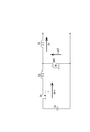
- FIG. 1 is a schematic circuit diagram illustrating a DC voltage converter according to a first embodiment.
- Schematic time chart showing the operation of the DC voltage converter
- Schematic partial circuit diagram showing the current flow of the DC voltage converter
- Schematic partial circuit diagram showing the current flow of the DC voltage converter
- Schematic partial circuit diagram showing the current flow of the DC voltage converter
- Schematic partial circuit diagram showing the current flow of the DC voltage converter
- Schematic partial circuit diagram showing the current flow of the DC voltage converter
- Schematic partial circuit diagram showing the current flow of the DC voltage converter Schematic time chart showing the operation of the DC voltage converter in Embodiment 2
- Partial circuit diagram showing another embodiment of the auxiliary capacitor Partial circuit diagram showing another embodiment of the auxiliary capacitor
- the DC voltage converter 10 is a so-called chopper type step-down DC-DC converter, which steps down a DC input voltage Vin applied from a battery as a main power source 40, It is converted into a DC output voltage Vout having a predetermined voltage value.
- the input voltage Vin is 48V, for example, and the output voltage Vout is 24V, for example.
- the DC voltage conversion device 10 is arranged for an HV vehicle on which a gasoline engine and a travel motor are mounted, and is applied to a power circuit that supplies power to a large-capacity load 50 such as a travel motor. Is done.
- the application of the DC voltage converter 10 is not limited to HV vehicles, and is not limited to vehicles.
- the load to which the DC voltage converter 10 is applied is not necessarily limited to a large capacity load.
- the present invention is not limited to a step-down DC-DC converter, and can be applied to a step-up DC-DC converter as will be described later.
- the DC voltage converter 10 includes an internal power line Ls, a first switch element SW1, a first parallel capacitor C1, a switch control unit 11, a low-pass filter 13, a reflux unit 14, and an auxiliary resonance circuit 20. including.
- the internal power supply line Ls is connected to the battery 40 and supplies the power from the battery 40 to each part of the DC voltage converter 10.
- the first switch element SW1 is configured by an N-channel MOSFET including a body diode D1.
- the drain terminal D of the first switch element SW1 is connected to the internal power supply line Ls.
- the first parallel capacitor C1 is connected in parallel to the first switch element SW1.
- the first parallel capacitor C1 is not limited to an individual element, and may be a parasitic capacitor of the first switch element SW1.
- the low-pass filter 13 is a well-known filter and includes, for example, a smoothing reactor Lo and a smoothing capacitor Co as shown in FIG.
- An input terminal 13a (corresponding to one end of the low-pass filter) of the low-pass filter 13 is connected to a source terminal S (corresponding to one end of the first switch element) of the first switch element SW1, and an output terminal 13b of the DC voltage converter 10 is connected. Connected to the output terminal.
- the low-pass filter 13 receives the potential Vn1 of the first connection point N1, that is, the first connection point voltage Vn1, and outputs the output voltage Vout obtained by smoothing the first connection point voltage Vn1.
- the reflux unit 14 is connected between the first connection point N1 and the ground line Lg, and is well known.
- the reflux unit 14 is configured by the second switch element SW2 as shown in FIG.
- the second switch element SW2 is configured by an N-channel MOSFET including a body diode D2, and is zero-voltage switched by the switch control unit 11.
- the second parallel capacitor C2 is connected in parallel to the second switch element SW2.
- the second parallel capacitor C2 can adjust the changing speed of the first connection point voltage Vn1 when the first switch element SW1 and the second switch element SW2 are in the off state, that is, the so-called dead time.
- the second parallel capacitor C2 is not limited to an individual element, like the first parallel capacitor C1, and may be a parasitic capacitor of the first switch element SW1.
- the reflux unit 14 is configured by the second switch element SW2, the setting of the reflux period can be appropriately performed by the on / off control of the second switch element SW2, and the switching of the second switch element SW2 by the zero voltage switching. Loss can be suppressed.
- the configuration of the reflux unit 14 is not limited to this, and may be configured by, for example, one reflux diode.
- the auxiliary resonant circuit 20 includes an auxiliary switch element SA, an auxiliary reactor LA, an auxiliary capacitor CA, and a voltage stabilizing diode D21 connected in series.
- the auxiliary resonance circuit 20 is connected to a first connection point N1 that is a connection point between the first switch element SW1 and the low-pass filter 13.
- one end La1 of the auxiliary reactor LA that is not connected to the auxiliary switch element SA is connected to the first connection point N1.
- the reactance of the auxiliary reactor LA is set to be sufficiently smaller than the smoothing reactor Lo.
- the auxiliary switch element SA is configured by an N-channel MOSFET in this embodiment.
- the auxiliary switch element SA includes a parasitic capacitance Cp and a body diode D3.
- the auxiliary switch element SA includes a drain terminal D, a gate terminal G, and a source terminal S.
- the source terminal S is connected to the other end La2 of the auxiliary reactor, and the drain terminal D of the source terminal S is turned on / off by a gate control signal GA applied to the gate terminal G.
- the source terminal S of the auxiliary switch element SA is an example of a “first terminal”
- the drain terminal D of the auxiliary switch element SA is an example of a “second terminal”.
- the voltage stabilizing diode D21 is connected between the second connection point N2, which is a connection point between the auxiliary reactor LA and the auxiliary switch element SA, and the ground line Lg. Specifically, the cathode of the voltage stabilization diode D21 is connected to the second connection point N2, and the anode of the voltage stabilization diode D21 is connected to the ground line Lg.
- the voltage stabilizing diode D21 stabilizes the drain-source voltage Vsa of the auxiliary switch element SA when the auxiliary switch element SA is off.
- the auxiliary capacitor CA is connected between the auxiliary switch element SA and the ground line Lg. Specifically, one end of the auxiliary capacitor CA is connected to the drain terminal D of the auxiliary switch element SA, and the other end of the auxiliary capacitor CA is connected to the ground line Lg.
- the drain terminal D of the auxiliary switch element SA corresponds to “one end of the auxiliary switch element on the side not connected to the auxiliary reactor”.
- the auxiliary capacitor CA supplies energy at the time of resonance of the auxiliary resonance circuit 20 by charging and discharging.
- the auxiliary capacitor CA has an energy when the first current Isw1 that flows through the first switch element SW1 and the second current Isw2 that flows through the second switch element SW2 exceed the output current (load current) Io. Charged using.
- the switch control unit 11 is connected to each switch element (SW1, SW2, SA), and generates a gate control signal (G1, G2, GA) for controlling on / off switching of each switch element. Specifically, the switch control unit 11 switches the first and second switch elements (SW1, SW2) by so-called zero voltage switching (ZVS) according to the gate control signals (G1, G2). The switch control unit 11 switches the auxiliary switch element SA by so-called zero current switching (ZCS) by the gate control signal GA.
- Each switch element (SW1, SW2, SA) is not limited to an N-channel MOSFET. For example, an IGBT or the like may be used.
- the auxiliary switch element SA is the gate control signal.
- the GA that is, when zero current switching (ZCS) is performed, the resonance operation by the auxiliary resonance circuit 20 is started.
- the resonance current Irs that is a current flowing through the auxiliary switch element SA and the auxiliary reactor LA is increased, and accordingly, the second current Isw2 that is a current flowing through the second switch element SW2 is decreased.
- the increasing speed of the resonance current Irs depends on the reactance magnitude of the auxiliary reactor LA.
- an output current (load current) Io that is a current flowing through the smoothing reactor Lo is constant. Note that the output current Io is substantially constant without being limited to the first period K1.
- the second switch element SW2 is turned off. As the second switch element SW2 is turned off, the second current Isw2 further decreases and becomes zero. On the other hand, the resonance current Irs increases and reaches the magnitude of the output current Io at time t1.
- FIG. 4 shows a current flow in a period (second period K2) from time t1 to time t2 when the first connection point voltage Vn1 becomes larger than the input voltage Vin.
- the resonance current Irs mainly includes the first parallel capacitor C1 and the second parallel capacitor C2. (See currents Ic1 and Ic2 in FIG. 4).
- the first parallel capacitor C1 is discharged, while the second parallel capacitor C2 is charged. Therefore, the first connection point voltage Vn1 increases.
- the first connection point voltage Vn1 is equal to the second voltage Vsw2 which is the drain-source voltage of the second switch element SW2. Therefore, as shown in FIG. 2, the second voltage Vsw2 increases in the second period K2.
- FIG. 5 shows a state from time t2 to time t3 (third period K3), which is a conduction period of the body diode D1. At this time, the first current Isw1 in the reverse direction flows through the body diode D1.
- the first switch element SW1 is turned on while the body diode D1 is conducting (time t3). That is, the first switch element SW1 is zero voltage switched (ZVS). At this time, a reverse voltage (input voltage Vin ⁇ auxiliary capacitor voltage (charging voltage) Vca) is applied to the auxiliary reactor LA. Then, as shown in FIG. 2, after time t3, the first current Isw1, which is the current flowing through the first switch element SW1, increases, and the resonance current Irs decreases. Then, after time t4 when the value of the first current Isw1 reaches the output current Io, the resonance current Irs becomes zero.
- 6A shows a current flow immediately after the first switch element SW1 is turned on at time t3, and FIG. 6B shows a period from time t3 to time t4 (fourth time). The current flow in period K4) is shown.
- the first switch element SW1 is turned off at time t5 after a predetermined time from time t4 when the resonance current Irs becomes zero.
- FIG. 6C shows a current flow in a period (fifth period K5) from time t4 to time t5.
- the first switch element SW1 When the first switch element SW1 is turned off at time t5, the first current Isw1 is commutated to the first parallel capacitor C1 and the second parallel capacitor C2 (see currents Ic1 and Ic2 in FIG. 7). At this time, the first connection point voltage Vn1 (second voltage Vsw2) drops rapidly. Then, after time t6 when the first connection point voltage Vn1 reaches zero V, the body diode D2 becomes conductive (see FIG. 8), and the second voltage Vsw2 is maintained at zero V. At this time, the second current Isw2 flows through the body diode D2.
- the second switch element SW2 is turned on, that is, zero voltage switching is performed, so-called synchronous rectification is started.
- charging of the auxiliary capacitor CA with the second current Isw2 is continued (see FIG. 9).
- the charging current (reverse resonance current) Irs decreases.
- auxiliary switch element SA is turned off, that is, zero current switching (ZCS) is performed. Synchronous rectification is continued for a period from time t8 to time t9 when the second switch element SW2 is turned off next. After time t9, the operation from time t0 is repeated. Note that one cycle from time t0 to time t9 is, for example, 10 ⁇ s (microseconds).
- FIG. 7 shows a current flow in a period (sixth period K6) from time t5 to time t6, which is the first half of the dead time
- FIG. 8 shows from time t6 to time t7, which is the second half of the dead time.
- the flow of current in the period (seventh period K7) is shown.
- the period from time t0 to time t4 corresponds to the discharging period KH of the auxiliary capacitor CA
- the period from time t4 to time t8 corresponds to the charging period KJ of the auxiliary capacitor CA.
- the voltage Vca when the auxiliary capacitor CA is discharged is determined by the capacity of the auxiliary capacitor CA.
- the charging period KJ as shown in FIG. 2, the period in which the first current Isw1 exceeds the output current Io (period from time t4 to time t5), and the second current Isw2 exceeds the output current Io.
- Period (period from time t6 to time t8).
- the ON period (from time t0 to time t8) of the gate control signal (an example of the control signal) GA of the auxiliary capacitor CA includes a charging period KJ.
- the on / off timing of each gate control signal is determined by a known method. That is, the on / off timing is determined by the switch control unit 11 based on a comparison between a detection signal from a detection circuit (not shown) that detects an electrical quantity such as the resonance current Irs and a reference value, for example. Alternatively, it is determined in advance by calculation based on circuit constants such as the reactance value of the auxiliary reactor LA and the capacity of the auxiliary capacitor CA. In this case, the determined timing data is stored in a memory or the like of the switch control unit 11, and the switch control unit 11 determines the on / off timing based on the stored data. Alternatively, the on / off timing is determined based on both the detection signal and the stored data.
- an auxiliary capacitor CA is connected to the auxiliary switch element SA of the auxiliary resonance circuit 20. Therefore, energy related to auxiliary resonance can be supplied from the auxiliary capacitor CA to the auxiliary resonance circuit 20.
- the first switch element SW1 and the second switch element SW2 are zero-voltage switched, and the auxiliary switch element SA is zero-current switched. Therefore, according to the direct-current voltage converter 10 of the first embodiment, high conversion efficiency can be maintained even when applied to a large-capacity load.
- the auxiliary capacitor CA can be charged using surplus energy generated during voltage conversion, and the auxiliary resonance circuit 20 can be operated by the energy stored in the auxiliary capacitor CA. Thereby, surplus energy related to voltage conversion can be effectively used, and conversion efficiency can be improved.
- the charging period (from time t6 to time t8 in FIG. 2) for charging the auxiliary capacitor CA by the second current Isw2 that exceeds the output current Io may not be included in the on period of the cate control signal GA.
- the on period of the gate control signal GA includes a charging period in which the auxiliary capacitor CA is charged with at least the first current Isw1 exceeding the output current Io.
- a voltage stabilizing diode D21 connected between the second connection point N2 and the ground line Lg is provided.
- the voltage stabilization diode D21 can stabilize the potential at the second connection point N2 during the period when the auxiliary switch element SA is off. That is, in the period when the auxiliary switch element SA21 is off and the second switch element SW2 is on (eighth period K8), when the N-channel MOSFET is used as the auxiliary switch element SA as in the first embodiment, the auxiliary switch element It is also conceivable that the potential at the second connection point N2 fluctuates due to oscillation through the parasitic capacitance Cp of SA, and the potential at the second connection point N2 rises higher than the input voltage Vin. However, at that time, the voltage stabilizing diode D21 suppresses the fluctuation of the potential at the second connection point N2. Note that the voltage stabilizing diode D21 may be omitted.
- each switch element can be set to substantially the same level as the input voltage Vin. Therefore, each switch element can be a component with a small rating, thereby reducing conduction loss.
- the switch control unit generates the ON period of the gate control signal GA of the auxiliary switch element SA by dividing it into a discharge period KH for discharging the auxiliary capacitor CA and a charge period KJ.
- the ON period of the gate control signal GA is changed from the time t0 to the time t8 in FIG. 2 so that the discharge period KH and the charging period KJ of the auxiliary capacitor CA are continuous. It is one period until immediately after.
- the on period of the gate control signal GA corresponds to the discharge period KH of the auxiliary capacitor CA, the period from time t0 to time t2 in FIG. It is divided into two periods from time t3 to time t5 in FIG.
- the first switch element SW1 is turned on at time t1 in the discharge period KH in FIG. 10, and the first switch element SW1 is turned off at time t4 in the charge period KJ in FIG.
- the second switch element SW2 is turned off at approximately time t0 in FIG. 10 which is the ON timing of the auxiliary switch element SA in the discharge period KH, and approximately time t5 in FIG.
- the second switch element SW2 is turned on.
- the ON period of the gate control signal GA of the auxiliary switch element SA is generated by being divided into the discharge period KH for discharging the auxiliary capacitor CA and the charge period KJ, so that the auxiliary period can be increased as compared with the case of the first embodiment.
- the period of the current flowing through the switch element SA can be shortened. Thereby, the conduction loss of the auxiliary switch element SA can be reduced.
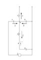
- the auxiliary capacitor includes a first auxiliary capacitor CA1 connected between the auxiliary switch element SA and the ground line Lg, and a connection point between the first auxiliary capacitor CA1 and the auxiliary switch element SA.
- a second auxiliary capacitor CA2 connected between N3 and the internal power supply line Ls may be used.
- the auxiliary capacitor may be constituted by an auxiliary capacitor CA connected between the auxiliary switch element and the internal power supply line. Even in these cases, an auxiliary resonance circuit using the energy stored in the auxiliary capacitor CA can be configured by the same control as in the above embodiment.
- the auxiliary switch element SA is configured by one auxiliary switch element SA
- the present invention is not limited to this.
- the auxiliary switch element SA may be configured by two auxiliary switch elements connected in series and controlled simultaneously by the switch control unit. It may be configured by one auxiliary switch element SA21.
- the reflux unit 14 is configured by the second switch element SW2 and the second parallel capacitor C2 is shown, but the present invention is not limited thereto.
- the reflux unit 14 may be configured by a single reflux diode.
- the DC voltage converter 10 is applied to a chopper type step-down DC-DC converter.
- the present invention is not limited to this.
- the DC voltage converter 10 is replaced with a chopper type boost DC-DC converter. It can also be applied to a DC converter.
- FIG. 11 shows an example of control and operation when the DC voltage converter 10 is applied to a chopper type step-up DC-DC converter.
Landscapes
- Engineering & Computer Science (AREA)
- Power Engineering (AREA)
- Dc-Dc Converters (AREA)
Abstract
直流電圧変換装置(10)は、内部電源線Lsに接続された第1スイッチ素子(SW1)と、ローパスフィルタ(13)と、直列接続された補助スイッチ素子(SA)と補助リアクトル(LA)とを含み、補助リアクトル(LA)の一端(La1)が第1スイッチ素子(SW1)とローパスフィルタ(13)との接続点である第1接続点(N1)に接続された補助共振回路(20)と、第1スイッチ素子(SW1)をゼロ電圧スイッチングし、補助スイッチ素子(SA)をゼロ電流スイッチングするスイッチ制御部(11)とを備える。補助共振回路(20)は、補助スイッチ素子(SA)の第2端子(D)と、グランド線(Lg)または内部電源線(Ls)との間に接続された補助コンデンサ(CA)を含む。
Description
本明細書に開示される技術は、直流電圧変換装置に関し、詳しくは、補助共振回路を備えた直流電圧変換装置に関する。
従来、スイッチング素子をいわゆるソフトスイッチングさせることによって、スイッチングによるスイッチング損失と高周波ノイズとを抑制するために、直流電圧変換装置に補助共振回路を備える方法が幅広く行われている。このような補助共振回路を備えた直流電圧変換装置として、例えば、特許文献1に開示されたDC-DCコンバータ(直流電圧変換装置)が知られている。この文献のDC-DCコンバータでは、平滑リアクトルに流れる電流に基づいて、第2の主スイッチ(ローサイドスイッチ)と補助共振回路に含まれる補助スイッチとが同時にオンされる期間を最適化することによって、無駄な電力損失の発生を防止するものである。
しかしながら、上記文献のDC-DCコンバータは、補助共振回路のエネルギー源、すなわち、電源は出力電圧Voutになっている。この出力電圧Voutは入力電圧Vinが変換されたものであるため、変換損失として補助共振回路での損失も上乗せされるこことなる。これは、コンバータの高効率化にとって有利であるとは言えなかった。また、このように出力電圧Voutを補助共振回路に印加する構成においては、入力電圧Vinを非常に低い出力電圧Voutに変換する場合、出力電圧Voutを補助共振回路に印加しても、文献1の図1のM点の電圧が入力電圧Vinに達せず、第1の主スイッチS1のソフトスイッチング(ゼロ電圧スイッチング)ができない虞があった。この場合、第1の主スイッチS1でのスイッチング損失が増加することとなる。
また、近年、直流電圧変換装置が、電気自動車等、大電流が必要とされるパワー回路として使用される場合、言い換えれば大容量負荷に使用される場合、微小な変換効率の低下が大きな変換損失となってしまう。そのため、大容量負荷に適用される際であっても高効率の変換効率を維持できる直流電圧変換装置が所望されていた。
本明細書に開示される技術は、上記のような事情に基づいて完成されたものであって、大容量負荷に適用される際に、高効率の変換効率を維持できる直流電圧変換装置を提供する。
本明細書に開示される直流電圧変換装置は、主電源から印加される直流の入力電圧を所定の電圧値を有する出力電圧に変換する直流電圧変換装置であって、前記主電源に接続される内部電源線と、前記内部電源線に接続された第1スイッチ素子と、一端が前記第1スイッチ素子の一端と接続されるローパスフィルタと、直列接続された補助スイッチ素子と補助リアクトルとを含み、前記補助リアクトルの一端が前記第1スイッチ素子と前記ローパスフィルタとの接続点である第1接続点に接続された補助共振回路と、前記第1接続点とグランド線との間に接続された還流部と、前記第1スイッチ素子をゼロ電圧スイッチングし、前記補助スイッチ素子をゼロ電流スイッチングするスイッチ制御部と、を備え、前記補助共振回路の前記補助スイッチ素子は、前記補助リアクトルの他端に接続された第1端子と、前記第1端子に対して接続がオンオフされる第2端子とを含み、前記補助共振回路は、前記補助スイッチ素子の前記第2端子と、グランド線または前記内部電源線との間に接続された補助コンデンサを含む。
本構成によれば、補助共振回路の補助スイッチ素子に補助コンデンサが接続されている。そのため、補助コンデンサから補助共振回路に補助共振に係るエネルギーを供給することができる。また、第1スイッチ素子はゼロ電圧スイッチングされ、補助スイッチ素子はゼロ電流スイッチングされる。そのため、本構成の直流電圧変換装置によれば、大容量負荷に適用される際であっても、高効率の変換効率を維持できる。
本構成によれば、補助共振回路の補助スイッチ素子に補助コンデンサが接続されている。そのため、補助コンデンサから補助共振回路に補助共振に係るエネルギーを供給することができる。また、第1スイッチ素子はゼロ電圧スイッチングされ、補助スイッチ素子はゼロ電流スイッチングされる。そのため、本構成の直流電圧変換装置によれば、大容量負荷に適用される際であっても、高効率の変換効率を維持できる。
上記直流電圧変換装置において、前記スイッチ制御部は、前記補助スイッチ素子をオンオフさせる制御信号を生成し、前記制御信号のオン期間は、少なくとも出力電流を超える前記第1スイッチ素子に流れる第1電流によって、前記補助コンデンサを充電する充電期間を含むようにしてもよい。
本構成によれば、電圧変換の際に生じる余剰エネルギーを用いて補助コンデンサが充電され、補助コンデンサに蓄えられたエネルギーによって補助共振回路を動作させることができる。それによって電圧変換に係る余剰エネルギーを効果的に利用でき、変換効率を向上させることができる。
本構成によれば、電圧変換の際に生じる余剰エネルギーを用いて補助コンデンサが充電され、補助コンデンサに蓄えられたエネルギーによって補助共振回路を動作させることができる。それによって電圧変換に係る余剰エネルギーを効果的に利用でき、変換効率を向上させることができる。
また、上記直流電圧変換装置において、前記スイッチ制御部は、前記制御信号の前記オン期間を、補助コンデンサを放電する放電期間と前記充電期間とに分けて生成するようにしてもよい。
本構成によれば、補助スイッチ素子のゲート制御信号のオン期間を、補助コンデンサを放電する放電期間と充電期間とに分けて生成することによって、補助スイッチ素子に流れる電流の期間を短くすることができる。それによって補助スイッチ素子の導通損失を低減できる。
また、上記直流電圧変換装置において、前記補助コンデンサは、前記補助スイッチ素子と前記グランド線との間に接続されているようにしてもよい。
本構成によれば、補助スイッチ素子のゲート制御信号のオン期間を、補助コンデンサを放電する放電期間と充電期間とに分けて生成することによって、補助スイッチ素子に流れる電流の期間を短くすることができる。それによって補助スイッチ素子の導通損失を低減できる。
また、上記直流電圧変換装置において、前記補助コンデンサは、前記補助スイッチ素子と前記グランド線との間に接続されているようにしてもよい。
本構成によれば、補助コンデンサの充放電制御が、補助コンデンサが補助スイッチ素子と内部電源線との間に接続される場合と比べて、簡易に行える。
また、上記直流電圧変換装置において、前記補助リアクトルと前記補助スイッチ素子との接続点である第2接続点と前記グランド線との間に接続された電圧安定化ダイオードをさらに備えるようにしてもよい。
本構成によれば、電圧安定化ダイオードによって、補助スイッチ素子がオフの期間における第2接続点の電位を安定化できる。すなわち、補助スイッチ素子がオフで第2スイッチ素子がオンの期間においては、補助スイッチ素子としてMOSFETが使用される場合、補助スイッチ素子の寄生容量を介して、第2接続点の電位が変動することが考えられる。その際、電圧安定化ダイオードによって第2接続点の電位の変動が抑制される。
本構成によれば、電圧安定化ダイオードによって、補助スイッチ素子がオフの期間における第2接続点の電位を安定化できる。すなわち、補助スイッチ素子がオフで第2スイッチ素子がオンの期間においては、補助スイッチ素子としてMOSFETが使用される場合、補助スイッチ素子の寄生容量を介して、第2接続点の電位が変動することが考えられる。その際、電圧安定化ダイオードによって第2接続点の電位の変動が抑制される。
また、上記直流電圧変換装置において、前記補助スイッチ素子は、直列に接続され、前記スイッチ制御部によって同一の制御信号によって制御される二個の補助スイッチ素子によって構成されるようにしてもよい。
本構成によれば、補助スイッチ素子を直列に接続された二個の補助スイッチ素子によって構成することによって、補助スイッチ素子としてのオン抵抗が増加する。それによって、補助スイッチ素子のオン時に流れるオン電流が低減されることによって、補助スイッチ素子のオン抵抗損失が、補助スイッチ素子が一個の場合と比べて低減される。なお、損失(電力)は電流の二乗に比例するため、この場合、オン抵抗の増加に伴うオン抵抗損失の増加量よりも、オン電流の低減によるオン抵抗損失の低下量の方が大きくなる。そのため、オン抵抗損失が低減される。
本構成によれば、補助スイッチ素子を直列に接続された二個の補助スイッチ素子によって構成することによって、補助スイッチ素子としてのオン抵抗が増加する。それによって、補助スイッチ素子のオン時に流れるオン電流が低減されることによって、補助スイッチ素子のオン抵抗損失が、補助スイッチ素子が一個の場合と比べて低減される。なお、損失(電力)は電流の二乗に比例するため、この場合、オン抵抗の増加に伴うオン抵抗損失の増加量よりも、オン電流の低減によるオン抵抗損失の低下量の方が大きくなる。そのため、オン抵抗損失が低減される。
また、上記直流電圧変換装置において、前記還流部は、前記スイッチ制御部によってゼロ電圧スイッチングされる第2スイッチ素子によって構成されるようにしてもよい。
本構成によれば、第2スイッチ素子のオンオフ制御によって還流期間の設定を適宜行えるとともに、ゼロ電圧スイッチングによって、第2スイッチ素子のスイッチング損失を抑制できる。
本構成によれば、第2スイッチ素子のオンオフ制御によって還流期間の設定を適宜行えるとともに、ゼロ電圧スイッチングによって、第2スイッチ素子のスイッチング損失を抑制できる。
また、上記直流電圧変換装置において、前記第1スイッチ素子に並列に接続された第1並列容量と、前記還流部に並列に接続された第2並列容量と、をさらに備えるようにしてもよい。
本構成によれば、第1スイッチ素子および第2スイッチ素子がオフされた際、いわゆるデッドタイムにおける、第1接続点の電位変化の速度を調整することができる。
本構成によれば、第1スイッチ素子および第2スイッチ素子がオフされた際、いわゆるデッドタイムにおける、第1接続点の電位変化の速度を調整することができる。
本明細書に開示される直流電圧変換装置によれば、大容量負荷に適用される際に、高効率の変換効率を維持できる。
<実施形態1>
実施形態1に直流電圧変換装置10を、図1から図9を参照しつつ説明する。
1.直流電圧変換装置の構成
直流電圧変換装置10は、本実施形態では、いわゆるチョッパ型の降圧DC-DCコンバータであり、主電源40であるバッッテリーから印加される直流の入力電圧Vinを降圧して、所定の電圧値を有する直流の出力電圧Voutに変換する。入力電圧Vinは、例えば、48Vであり、出力電圧Voutは、例えば、24Vである。
実施形態1に直流電圧変換装置10を、図1から図9を参照しつつ説明する。
1.直流電圧変換装置の構成
直流電圧変換装置10は、本実施形態では、いわゆるチョッパ型の降圧DC-DCコンバータであり、主電源40であるバッッテリーから印加される直流の入力電圧Vinを降圧して、所定の電圧値を有する直流の出力電圧Voutに変換する。入力電圧Vinは、例えば、48Vであり、出力電圧Voutは、例えば、24Vである。
直流電圧変換装置10は、本実施形態では、例えば、ガソリンエンジンと走行用モータとが搭載されたHV車用に配置され、走行用モータ等の大容量負荷50に電力を供給するパワー回路に適用される。なお、直流電圧変換装置10の適用は、HV車に限られず、また車両にも限られない。また、直流電圧変換装置10が適用される負荷は、必ずしも大容量負荷に限られない。さらには、降圧DC-DCコンバータにも限られず、後述するように昇圧DC-DCコンバータにも適用できる。
直流電圧変換装置10は、図1に示されるように、内部電源線Ls、第1スイッチ素子SW1、第1並列容量C1、スイッチ制御部11、ローパスフィルタ13、還流部14、および補助共振回路20を含む。
内部電源線Lsは、バッッテリー40に接続され、バッッテリー40からの電力を直流電圧変換装置10の各部に供給する。
第1スイッチ素子SW1は、本実施形態ではボディダイオードD1を含むNチャネルMOSFETによって構成されている。第1スイッチ素子SW1のドレイン端子Dが内部電源線Lsに接続されている。
第1並列容量C1は、第1スイッチ素子SW1に並列に接続されている。なお、第1並列容量C1は個別の素子に限られず、第1スイッチ素子SW1の寄生容量であってもよい。
ローパスフィルタ13は周知のものであり、図1に示されるように、例えば、平滑リアクトルLoおよび平滑コンデンサCoによって構成される。ローパスフィルタ13の入力端13a(ローパスフィルタの一端に相当)は第1スイッチ素子SW1のソース端子S(第1スイッチ素子の一端に相当)と接続され、その出力端13bは直流電圧変換装置10の出力端に接続される。ローパスフィルタ13は、第1接続点N1の電位Vn1、すなわち第1接続点電圧Vn1を入力し、第1接続点電圧Vn1が平滑された出力電圧Voutを出力する。
還流部14は第1接続点N1とグランド線Lgとの間に接続され、周知のものである。本実施形態では、還流部14は、図1に示されるように、第2スイッチ素子SW2によって構成される。第2スイッチ素子SW2は、ボディダイオードD2を含むNチャネルMOSFETによって構成され、スイッチ制御部11によってゼロ電圧スイッチングされる。
第2並列容量C2は、第2スイッチ素子SW2に並列に接続される。第2並列容量C2によって、第1スイッチ素子SW1および第2スイッチ素子SW2がオフ状態、いわゆるデッドタイムにおける、第1接続点電圧Vn1の変化速度を調整することができる。なお、第2並列容量C2は、第1並列容量C1と同様に、個別の素子に限られず、第1スイッチ素子SW1の寄生容量であってもよい。
このように、還流部14が第2スイッチ素子SW2によって構成されることによって、第2スイッチ素子SW2のオンオフ制御によって還流期間の設定を適宜行えるとともに、ゼロ電圧スイッチングによって、第2スイッチ素子SW2のスイッチング損失を抑制できる。なお、還流部14の構成はこれに限られず、例えば、一個の還流ダイオードによって構成されてもよい。
補助共振回路20は、直列接続された、補助スイッチ素子SAと補助リアクトルLA、補助コンデンサCA、および電圧安定化ダイオードD21を含む。補助共振回路20は、第1スイッチ素子SW1とローパスフィルタ13との接続点である第1接続点N1に接続されている。詳細には、補助スイッチ素子SAに接続されていない補助リアクトルLAの一端La1が、第1接続点N1に接続されている。なお、ここで補助リアクトルLAのリアクタンスは、平滑リアクトルLoに比べて、十分小さくなるように設定されている。
補助スイッチ素子SAは、本実施形態においてはNチャネルMOSFETによって構成されている。補助スイッチ素子SAは、寄生容量CpおよびボディダイオードD3を含む。補助スイッチ素子SAは、ドレイン端子D、ゲート端子G、およびソース端子Sを含む。そのソース端子Sは補助リアクトルの他端La2に接続され、そのドレイン端子Dは、ソース端子Sに対する接続が、ゲート端子Gに印加されるゲート制御信号GAによってオンオフされる。ここで、補助スイッチ素子SAのソース端子Sは「第1端子」の一例であり、補助スイッチ素子SAのドレイン端子Dは「第2端子」の一例である。
電圧安定化ダイオードD21は、補助リアクトルLAと補助スイッチ素子SAとの接続点である第2接続点N2とグランド線Lgとの間に接続されている。詳細には、電圧安定化ダイオードD21のカソードが第2接続点N2に接続され、電圧安定化ダイオードD21のアノードがグランド線Lgに接続されている。電圧安定化ダイオードD21は、補助スイッチ素子SAのオフ時に、補助スイッチ素子SAのドレイン-ソース間の電圧Vsaを安定化させる。
補助コンデンサCAは、補助スイッチ素子SAとグランド線Lgとの間に接続される。詳しくは、補助コンデンサCAの一端が補助スイッチ素子SAのドレイン端子Dに接続され、補助コンデンサCAの他端がグランド線Lgに接続される。ここで、補助スイッチ素子SAのドレイン端子Dは、「補助スイッチ素子の補助リアクトルに接続されていない側の一端」に相当する。補助コンデンサCAは、充放電によって補助共振回路20の共振時のエネルギーを供給する。補助コンデンサCAは、第1スイッチ素子SW1を流れる電流である第1電流Isw1、および第2スイッチ素子SW2を流れる電流である第2電流Isw2が、出力電流(負荷電流)Ioを上回る際のエネルキーを利用して充電される。
スイッチ制御部11は、各スイッチ素子(SW1、SW2、SA)に接続され、各スイッチ素子のオンオフのスイッチングを制御するゲート制御信号(G1、G2、GA)を生成する。詳細には、スイッチ制御部11は、ゲート制御信号(G1、G2)によって、第1、第2スイッチ素子(SW1、SW2)を、いわゆるゼロ電圧スイッチング(ZVS)によってスイッチングする。また、スイッチ制御部11は、ゲート制御信号GAによって、補助スイッチ素子SAを、いわゆるゼロ電流スイッチング(ZCS)によってスイッチングする。なお、各スイッチ素子(SW1、SW2、SA)は、NチャネルMOSFETに限られない。例えば、IGBT等であってもよい。
2.直流電圧変換装置の動作
次に、図2から図9を参照しつつ直流電圧変換装置10の動作を説明する。
次に、図2から図9を参照しつつ直流電圧変換装置10の動作を説明する。
図2に示されるように、第1スイッチ素子SW1がオフ状態で、第2スイッチ素子SW2はオン状態である還流状態、言い換えれば、同期整流状態の時刻t0において、補助スイッチ素子SAがゲート制御信号GAによってオンされると、すなわち、ゼロ電流スイッチング(ZCS)されると、補助共振回路20による共振動作が開始される。
すると、時刻t0から時刻t1までの期間である第1期間K1において、図3に示されように電流が流れる。すなわち、補助スイッチ素子SAおよび補助リアクトルLAに流れる電流である共振電流Irsが増加し、それに伴って第2スイッチ素子SW2に流れる電流である第2電流Isw2が減少する。共振電流Irsの増加速度は補助リアクトルLAのリアクタンスの大きさに依存する。第1期間K1において、平滑リアクトルLoを流れる電流である出力電流(負荷電流)Ioは一定である。なお、第1期間K1に限られず、出力電流Ioは、ほぼ一定とする。
第1期間K1内において、第2スイッチ素子SW2がオフされる。第2スイッチ素子SW2のオフに伴って、第2電流Isw2がさらに減少しゼロとなる。一方、共振電流Irsが増加して、時刻t1において出力電流Ioの大きさに達する。
図4には、時刻t1から第1接続点電圧Vn1が入力電圧Vinより大きくなる時刻t2までの期間(第2期間K2)における電流の流れが、示される。第2期間K2において、第1、第2スイッチ素子(SW1、SW2)がオフ状態(いわゆる、デッドタイム)であるため、共振電流Irsは、主に、第1並列容量C1および第2並列容量C2を介して流れる(図4の電流Ic1、Ic2参照)。このとき、第1並列容量C1は放電し、一方、第2並列容量C2は充電される。そのため、第1接続点電圧Vn1が上昇する。なお、ここで、第1接続点電圧Vn1と、第2スイッチ素子SW2のドレイン-ソース間電圧である第2電圧Vsw2とは等しい。そのため、図2に示されるように、第2期間K2において第2電圧Vsw2は上昇する。
そして、時刻t2において、第1接続点電圧Vn1(第2電圧Vsw2)が入力電圧Vinに達すると、第1スイッチ素子SW1のボディダイオードD1が導通して、第1スイッチ素子SW1のドレイン-ソース間電圧である第1電圧Vsw1がゼロとなる。図5に、ボディダイオードD1の導通期間である時刻t2から時刻t3(第3期間K3)の状態が示される。このとき、ボディダイオードD1を介して逆方向の第1電流Isw1が流れる。
そして、ボディダイオードD1の導通中に、第1スイッチ素子SW1がオンされる(時刻t3)。すなわち、第1スイッチ素子SW1がゼロ電圧スイッチング(ZVS)される。このとき、補助リアクトルLAには逆方向の電圧(入力電圧Vin-補助コンデンサ電圧(充電電圧)Vca)が印加される。すると、図2に示されるように、時刻t3以降において、第1スイッチ素子SW1に流れる電流である第1電流Isw1が増加するとともに、共振電流Irsが減少する。そして第1電流Isw1の値が出力電流Ioに達する時刻t4の後において、共振電流Irsがゼロとなる。図6の(a)には、時刻t3において第1スイッチ素子SW1がオンされた直後における電流の流れが示され、図6の(b)には、時刻t3から時刻t4までの期間(第4期間K4)における電流の流れが示される。
そして、共振電流Irsがゼロとなる時刻t4から所定時刻後の時刻t5において、第1スイッチ素子SW1がオフされる。図6の(c)には、時刻t4から時刻t5までの期間(第5期間K5)における電流の流れが示される。
時刻t5において第1スイッチ素子SW1がオフされると、第1電流Isw1が、第1並列容量C1および第2並列容量C2に転流される(図7の電流Ic1、Ic2参照)。このとき、第1接続点電圧Vn1(第2電圧Vsw2)が急激に降下する。そして、第1接続点電圧Vn1がゼロVに達する時刻t6以降において、ボディダイオードD2が導通(図8参照)し、第2電圧Vsw2がゼロVに維持される。このとき、ボディダイオードD2を介して第2電流Isw2が流れる。
そして、ボディダイオードD2が導通する時刻t6以降の時刻t7において、第2スイッチ素子SW2がオンされて、すなわち、ゼロ電圧スイッチングされて、いわゆる同期整流が開始される。このとき第2電流Isw2による補助コンデンサCAへの充電は継続される(図9参照)。そして補助コンデンサCAの充電電圧Vcaの上昇に伴い充電電流(逆方向の共振電流)Irsが減少する。
共振電流Irsがゼロに達する時刻t8において補助スイッチ素子SAがオフ、すなわち、ゼロ電流スイッチング(ZCS)される。時刻t8から次に第2スイッチ素子SW2がオフされる時刻t9までの期間は同期整流が継続される。時刻t9以降は、上記時刻t0からの動作が繰り返される。なお、時刻t0から時刻t9までの1周期は、例えば、10μs(マイクロ秒)である。
ここで、時刻t5から時刻t7までの期間は、いわゆるデッドタイムである。図7には、デッドタイムの前半である時刻t5から時刻t6までの期間(第6期間K6)における電流の流れが示され、図8には、デッドタイムの後半である時刻t6から時刻t7までの期間(第7期間K7)における電流の流れが示される。
また、時刻t0から時刻t4までが補助コンデンサCAの放電期間KHに相当し、時刻t4から時刻t8までが補助コンデンサCAの充電期間KJに相当する。なお、補助コンデンサCAの放電時の電圧Vcaは、補助コンデンサCAの容量によって決まる。
ここで、充電期間KJには、図2に示されるように、第1電流Isw1が出力電流Ioを超える期間(時刻t4から時刻t5までの期間)と、第2電流Isw2が出力電流Ioを超える期間(時刻t6から時刻t8までの期間)とが含まれる。そして、補助コンデンサCAのゲート制御信号(制御信号の一例)GAのオン期間(時刻t0から時刻t8)は、充電期間KJを含む。すなわち、補助コンデンサCAのゲート制御信号(制御信号の一例)GAのオン期間は、出力電流Ioを超える第1電流Isw1、および出力電流Ioを超える第2電流Isw2によって、補助コンデンサCAを充電する充電期間KJを含む。
なお、補助スイッチ素子SAがオフされ、補助スイッチ素子SAおよびボディダイオードD3に流れる電流がゼロとなった時刻t8以降において、補助スイッチ素子SAの寄生容量Cpを介して流れる電流によって、発振することが考えられる。詳しくは、補助リアクトルLA、寄生容量Cp、補助スイッチ素子SA、および第2スイッチ素子SW2によって形成される回路において、補助スイッチ素子SAのドレイン-ソース間の電圧Vsaが発振によって大きく振動することが考えられる。しかしながら、このような、電圧Vsaの振動の発生は、電圧安定化ダイオードD21によって抑制することができる。
ここで、各ゲート制御信号(G1、G2、GA)のオンオフタイミングの決定は、周知の方法によって行われる。すなわち、オンオフタイミングは、例えば、共振電流Irs等の電気量を検知する検知回路(図示せず)からの検知信号と、基準値との比較に基づいて、スイッチ制御部11によって決定される。または、補助リアクトルLAのリアクタンス値、補助コンデンサCAの容量等の回路定数に基づく計算によって予め決定される。この場合、決定されたタイミングデータがスイッチ制御部11のメモリ等に格納され、スイッチ制御部11は、その格納データに基づいてオンオフタイミングを決定する。あるいは、オンオフタイミングは、検知信号と格納データの両方に基づいて決定される。
3.実施形態1の効果
実施形態1では、補助共振回路20の補助スイッチ素子SAに補助コンデンサCAが接続されている。そのため、補助コンデンサCAから補助共振回路20に補助共振に係るエネルギーを供給することができる。また、第1スイッチ素子SW1および第2スイッチ素子SW2はゼロ電圧スイッチングされ、補助スイッチ素子SAはゼロ電流スイッチングされる。そのため、実施形態1の直流電圧変換装置10によれば、大容量負荷に適用される際であっても、高効率の変換効率を維持できる。
実施形態1では、補助共振回路20の補助スイッチ素子SAに補助コンデンサCAが接続されている。そのため、補助コンデンサCAから補助共振回路20に補助共振に係るエネルギーを供給することができる。また、第1スイッチ素子SW1および第2スイッチ素子SW2はゼロ電圧スイッチングされ、補助スイッチ素子SAはゼロ電流スイッチングされる。そのため、実施形態1の直流電圧変換装置10によれば、大容量負荷に適用される際であっても、高効率の変換効率を維持できる。
また、スイッチ制御部11が生成する、補助スイッチ素子SAのケート制御信号GAのオン期間(図2の時刻t0から時刻t8まで)は、出力電流Ioを超える第1電流Isw1、および出力電流Ioを超える第2電流Isw2によって、補助コンデンサCAを充電する充電期間(図2の時刻t4から時刻t5まで、および時刻t6から時刻t8まで)を含む。そのため、電圧変換の際に生じる余剰エネルギーを用いて補助コンデンサCAを充電して、補助コンデンサCAに蓄えられたエネルギーによって補助共振回路20を動作させることができる。それによって電圧変換に係る余剰エネルギーを効果的に利用でき、変換効率を向上させることができる。
なお、ケート制御信号GAのオン期間には、出力電流Ioを超える第2電流Isw2によって、補助コンデンサCAを充電する充電期間(図2の時刻t6から時刻t8まで)は含まれなくてもよい。要は、ケート制御信号GAのオン期間には、少なくとも出力電流Ioを超える第1電流Isw1によって、補助コンデンサCAを充電する充電期間を含むものであればよい。
また、実施形態1では、第2接続点N2とグランド線Lgとの間に接続された電圧安定化ダイオードD21が設けられている。電圧安定化ダイオードD21によって、補助スイッチ素子SAがオフの期間における第2接続点N2の電位を安定化できる。すなわち、補助スイッチ素子SA21がオフで第2スイッチ素子SW2がオンの期間(第8期間K8)においては、実施形態1のように補助スイッチ素子SAとしてNチャネルMOSFETが使用される場合、補助スイッチ素子SAの寄生容量Cpを介した発振によって、第2接続点N2の電位が変動し、第2接続点N2の電位が入力電圧Vinより大きく上昇することも考えられる。しかしながら、その際、電圧安定化ダイオードD21によって第2接続点N2の電位の変動が抑制される。なお、電圧安定化ダイオードD21は、省略されてもよい。
また、各スイッチ素子(SW1、SW2、SA)に印加される電圧を入力電圧Vinとほぼ同一レベルにできる。そのため、各スイッチ素子を定格の小さい部品とすることができ、それによって導通損失を低減できる。
<実施形態2>
実施形態2を、図10を参照して説明する。実施形態1とはスイッチ制御部11が生成する各スイッチ素子(SW1、SW2、SA)のゲート制御信号(G1、G2、GA)のオンオフタイミングのみが異なる。そのため、以下において、ゲート制御信号(G1、G2、GA)のオンオフタイミングの相違点のみを説明する。
実施形態2を、図10を参照して説明する。実施形態1とはスイッチ制御部11が生成する各スイッチ素子(SW1、SW2、SA)のゲート制御信号(G1、G2、GA)のオンオフタイミングのみが異なる。そのため、以下において、ゲート制御信号(G1、G2、GA)のオンオフタイミングの相違点のみを説明する。
実施形態2では、スイッチ制御部は、特に、補助スイッチ素子SAのゲート制御信号GAのオン期間を、補助コンデンサCAを放電する放電期間KHと充電期間KJとに分けて生成する。
すなわち、実施形態1では、図2に示されるように、補助コンデンサCAの放電期間KHと充電期間KJとが連続するように、ゲート制御信号GAのオン期間が、図2の時刻t0から時刻t8の直後までの期間の一期間とされている。しかしながら、実施形態2では、図10に示されるように、ゲート制御信号GAのオン期間が、補助コンデンサCAの放電期間KHに相当する、図10の時刻t0から時刻t2までの期間と、充電期間KJにほぼ相当する、図10の時刻t3から時刻t5までの二つの期間に分けられている。
そして、図10の放電期間KH中の時刻t1において第1スイッチ素子SW1がオンされ、図10の充電期間KJ中の時刻t4において第1スイッチ素子SW1がオフされる。
また、放電期間KHにおける補助スイッチ素子SAのオンタイミングである図10のほぼ時刻t0において第2スイッチ素子SW2がオフされ、充電期間KJにおける補助スイッチ素子SAのオフタイミングである図10のほぼ時刻t5において第2スイッチ素子SW2がオンされる。
このように、補助スイッチ素子SAのゲート制御信号GAのオン期間を、補助コンデンサCAを放電する放電期間KHと充電期間KJとに分けて生成することによって、実施形態1の場合と比べて、補助スイッチ素子SAに流れる電流の期間を短くすることができる。それによって補助スイッチ素子SAの導通損失を低減できる。
<他の実施形態>
本発明は上記記述および図面によって説明した実施形態に限定されるものではなく、例えば次のような実施形態も本発明の技術的範囲に含まれる。
<他の実施形態>
本発明は上記記述および図面によって説明した実施形態に限定されるものではなく、例えば次のような実施形態も本発明の技術的範囲に含まれる。
(1)上記実施形態では、補助コンデンサを補助スイッチ素子と前記グランド線との間に接続されている補助コンデンサCAによって構成する例を示したが、これに限られない。例えば、補助コンデンサを、図11に示されるように、補助スイッチ素子SAとグランド線Lgとの間に接続された第1補助コンデンサCA1と、第1補助コンデンサCA1と補助スイッチ素子SAとの接続点N3と内部電源線Lsとの間に接続された第2補助コンデンサCA2とによって構成されるようにしてもよい。この場合、各コンデンサの容量は、ほぼ、CA=2×CA1=2×CA2とすることが好ましい。
あるいは、補助コンデンサを、図12に示されるように、補助スイッチ素子と内部電源線との間に接続されている補助コンデンサCAによって構成するようにしてもよい。これらの場合であっても、上記実施形態と同様な制御によって、補助コンデンサCAに蓄えられたエネルギーを利用した補助共振回路を構成することができる。
(2)上記実施形態では、補助スイッチ素子SAを、一個の補助スイッチ素子SAによって構成する例を示したが、これに限られない。例えば、補助スイッチ素子SAは、直列に接続され、スイッチ制御部によって同時に制御される二個の補助スイッチ素子によって構成されるようにしてもよい。
一個の補助スイッチ素子SA21によって構成されてもよい。
一個の補助スイッチ素子SA21によって構成されてもよい。
(3)上記実施形態では、還流部14が第2スイッチ素子SW2と第2並列容量C2とによって構成される例を示したがこれに限られない。例えば、還流部14は、一個の還流ダイオードによって構成されてもよい。
(4)上記実施形態では、直流電圧変換装置10をチョッパ型の降圧DC-DCコンバータに適用する例を示したが、これに限られず、例えば、直流電圧変換装置10をチョッパ型の昇圧DC-DCコンバータに適用することもできる。図11に、直流電圧変換装置10をチョッパ型の昇圧DC-DCコンバータに適用した際の、制御および動作の例を示す。
10…直流電圧変換装置
11…スイッチ制御部
13…ローパスフィルタ
14…還流部(第2スイッチ素子)
20…補助共振回路
40…主電源
C1…第1並列容量
C2…第2並列容量
CA…補助コンデンサ
D…第2スイッチ素子のドレイン端子(第2端子)
D21…電圧安定化ダイオード
LA…補助リアクトル
Lg…グランド線
Ls…内部電源線
N1…第1接続点
N2…第2接続点
S…第2スイッチ素子のソース端子(第1端子)
SA…補助スイッチ素子
SW1…第1スイッチ素子(NチャネルMOSFET)
SW2…第2スイッチ素子(NチャネルMOSFET)
11…スイッチ制御部
13…ローパスフィルタ
14…還流部(第2スイッチ素子)
20…補助共振回路
40…主電源
C1…第1並列容量
C2…第2並列容量
CA…補助コンデンサ
D…第2スイッチ素子のドレイン端子(第2端子)
D21…電圧安定化ダイオード
LA…補助リアクトル
Lg…グランド線
Ls…内部電源線
N1…第1接続点
N2…第2接続点
S…第2スイッチ素子のソース端子(第1端子)
SA…補助スイッチ素子
SW1…第1スイッチ素子(NチャネルMOSFET)
SW2…第2スイッチ素子(NチャネルMOSFET)
Claims (8)
- 主電源から印加される直流の入力電圧を所定の電圧値を有する出力電圧に変換する直流電圧変換装置であって、
前記主電源に接続される内部電源線と、
前記内部電源線に接続された第1スイッチ素子と
一端が前記第1スイッチ素子の一端と接続されるローパスフィルタと、
直列接続された補助スイッチ素子と補助リアクトルとを含み、前記補助リアクトルの一端が前記第1スイッチ素子と前記ローパスフィルタとの接続点である第1接続点に接続された補助共振回路と、
前記第1接続点とグランド線との間に接続された還流部と、
前記第1スイッチ素子をゼロ電圧スイッチングし、前記補助スイッチ素子をゼロ電流スイッチングするスイッチ制御部と、を備え、
前記補助共振回路の前記補助スイッチ素子は、前記補助リアクトルの他端に接続された第1端子と、前記第1端子に対して接続がオンオフされる第2端子とを含み、
前記補助共振回路は、
前記補助スイッチ素子の前記第2端子と、グランド線または前記内部電源線との間に接続された補助コンデンサを含む、直流電圧変換装置。 - 請求項1に記載の直流電圧変換装置において、
前記スイッチ制御部は、前記補助スイッチ素子をオンオフさせる制御信号を生成し、
前記制御信号のオン期間は、少なくとも出力電流を超える前記第1スイッチ素子に流れる第1電流によって、前記補助コンデンサを充電する充電期間を含む、直流電圧変換装置。 - 請求項2に記載の直流電圧変換装置において、
前記スイッチ制御部は、前記制御信号のオン期間を、補助コンデンサを放電する放電期間と前記充電期間とに分けて生成する、直流電圧変換装置。 - 請求項1から請求項3の何れか一項に記載の直流電圧変換装置において、
前記補助コンデンサは、前記補助スイッチ素子と前記グランド線との間に接続されている、直流電圧変換装置。 - 請求項1から請求項4の何れか一項に記載の直流電圧変換装置において、
前記補助リアクトルと前記補助スイッチ素子との接続点である第2接続点と前記グランド線との間に接続された電圧安定化ダイオードをさらに備える、直流電圧変換装置。 - 請求項1から請求項5の何れか一項に記載の直流電圧変換装置において、
前記補助スイッチ素子は、直列に接続され、前記スイッチ制御部によって同一の制御信号によって制御される二個の補助スイッチ素子によって構成される、直流電圧変換装置。 - 請求項1から請求項6の何れか一項に記載の直流電圧変換装置において、
前記還流部は、前記スイッチ制御部によってゼロ電圧スイッチングされる第2スイッチ素子によって構成される、直流電圧変換装置。 - 請求項1から請求項7の何れか一項に記載の直流電圧変換装置において、
前記第1スイッチ素子に並列に接続された第1並列容量と、
前記還流部に並列に接続された第2並列容量と、をさらに備える、直流電圧変換装置。
Priority Applications (2)
| Application Number | Priority Date | Filing Date | Title |
|---|---|---|---|
| CN201880012565.8A CN110692185A (zh) | 2017-03-07 | 2018-02-20 | 直流电压转换装置 |
| DE112018001219.0T DE112018001219T5 (de) | 2017-03-07 | 2018-02-20 | Gleichspannungswandler |
Applications Claiming Priority (2)
| Application Number | Priority Date | Filing Date | Title |
|---|---|---|---|
| JP2017042872A JP2018148725A (ja) | 2017-03-07 | 2017-03-07 | 直流電圧変換装置 |
| JP2017-042872 | 2017-03-07 |
Publications (1)
| Publication Number | Publication Date |
|---|---|
| WO2018163794A1 true WO2018163794A1 (ja) | 2018-09-13 |
Family
ID=63448896
Family Applications (1)
| Application Number | Title | Priority Date | Filing Date |
|---|---|---|---|
| PCT/JP2018/005840 WO2018163794A1 (ja) | 2017-03-07 | 2018-02-20 | 直流電圧変換装置 |
Country Status (4)
| Country | Link |
|---|---|
| JP (1) | JP2018148725A (ja) |
| CN (1) | CN110692185A (ja) |
| DE (1) | DE112018001219T5 (ja) |
| WO (1) | WO2018163794A1 (ja) |
Families Citing this family (2)
| Publication number | Priority date | Publication date | Assignee | Title |
|---|---|---|---|---|
| CN112054689A (zh) * | 2020-08-30 | 2020-12-08 | 哈尔滨工程大学 | 一种隔离三电平直流变换器 |
| WO2022047633A1 (zh) * | 2020-09-01 | 2022-03-10 | 华为数字能源技术有限公司 | 一种dc/dc变换器、电压增益切换方法及系统 |
Citations (5)
| Publication number | Priority date | Publication date | Assignee | Title |
|---|---|---|---|---|
| JPH06269165A (ja) * | 1993-03-11 | 1994-09-22 | Sanken Electric Co Ltd | Pwm型dc−dcコンバータ |
| US5410467A (en) * | 1992-03-19 | 1995-04-25 | Astec International Limited | Power converters with improved switching efficiency |
| JPH11178319A (ja) * | 1997-12-12 | 1999-07-02 | Toyo Electric Mfg Co Ltd | 補助共振転流回路付電力変換装置のゲート信号制御方法 |
| JP2002171759A (ja) * | 2000-05-10 | 2002-06-14 | Hitachi Medical Corp | Dc−dcコンバータ及びこれを用いたx線高電圧装置 |
| JP2002252965A (ja) * | 2001-02-22 | 2002-09-06 | Denso Corp | 補助共振転流回路を用いた電力変換装置 |
Family Cites Families (5)
| Publication number | Priority date | Publication date | Assignee | Title |
|---|---|---|---|---|
| JP3401772B2 (ja) * | 1993-08-23 | 2003-04-28 | 株式会社ユアサコーポレーション | 部分共振pwmインバータ |
| JP4304862B2 (ja) * | 2000-12-28 | 2009-07-29 | 富士電機システムズ株式会社 | 電力変換装置 |
| JP4017490B2 (ja) * | 2002-10-02 | 2007-12-05 | 株式会社デンソー | Dc/dcコンバータ |
| JP4193606B2 (ja) * | 2003-06-26 | 2008-12-10 | 株式会社デンソー | Dc/dcコンバータ |
| US7548435B2 (en) * | 2006-03-31 | 2009-06-16 | Astec International Limited | Zero-voltage-switching DC-DC converters with synchronous rectifiers |
-
2017
- 2017-03-07 JP JP2017042872A patent/JP2018148725A/ja active Pending
-
2018
- 2018-02-20 DE DE112018001219.0T patent/DE112018001219T5/de not_active Withdrawn
- 2018-02-20 WO PCT/JP2018/005840 patent/WO2018163794A1/ja active Application Filing
- 2018-02-20 CN CN201880012565.8A patent/CN110692185A/zh active Pending
Patent Citations (5)
| Publication number | Priority date | Publication date | Assignee | Title |
|---|---|---|---|---|
| US5410467A (en) * | 1992-03-19 | 1995-04-25 | Astec International Limited | Power converters with improved switching efficiency |
| JPH06269165A (ja) * | 1993-03-11 | 1994-09-22 | Sanken Electric Co Ltd | Pwm型dc−dcコンバータ |
| JPH11178319A (ja) * | 1997-12-12 | 1999-07-02 | Toyo Electric Mfg Co Ltd | 補助共振転流回路付電力変換装置のゲート信号制御方法 |
| JP2002171759A (ja) * | 2000-05-10 | 2002-06-14 | Hitachi Medical Corp | Dc−dcコンバータ及びこれを用いたx線高電圧装置 |
| JP2002252965A (ja) * | 2001-02-22 | 2002-09-06 | Denso Corp | 補助共振転流回路を用いた電力変換装置 |
Also Published As
| Publication number | Publication date |
|---|---|
| JP2018148725A (ja) | 2018-09-20 |
| CN110692185A (zh) | 2020-01-14 |
| DE112018001219T5 (de) | 2019-11-21 |
Similar Documents
| Publication | Publication Date | Title |
|---|---|---|
| US9438115B2 (en) | Power supply system | |
| Moo et al. | Twin-buck converter with zero-voltage transition | |
| TWI473394B (zh) | 切換式電源供應器及其驅動電路與控制方法 | |
| US7486055B2 (en) | DC-DC converter having a diode module with a first series circuit and a second series with a flywheel diode | |
| WO2012144249A1 (ja) | 電力変換装置およびそれを備えた車載電源装置 | |
| JP6771156B2 (ja) | 電力変換装置 | |
| WO2008020629A1 (fr) | Convertisseur cc/cc à commutation souple pousser-tirer de type poussée d'isolation | |
| US20060255777A1 (en) | Apparatus and method for improving voltage converter low load efficiency | |
| WO2010107060A1 (ja) | Dc-dcコンバータ | |
| CN113972836B (zh) | 一种三电平升压变换器及控制方法 | |
| JP6452226B2 (ja) | Dc−dcコンバータの補助回路及びその補助回路を用いた双方向昇降圧dc−dcコンバータ | |
| JP2013236428A (ja) | 直流変換装置 | |
| Barner et al. | A 10 MHz, 48-to-5V synchronous converter with dead time enabled 125 ps resolution zero-voltage switching | |
| WO2018163794A1 (ja) | 直流電圧変換装置 | |
| CN109617407B (zh) | 一种升压式串并联全谐振开关电容变换器 | |
| CN109309448B (zh) | 一种宽输入宽输出Cuk DC-DC变换器 | |
| CN209170226U (zh) | 一种新型可扩展Zeta DC-DC变换器 | |
| JP2004312913A (ja) | 降圧型dc−dcコンバータ | |
| CN109274267B (zh) | 一种新型可扩展Zeta DC-DC变换器 | |
| WO2010098486A1 (ja) | Dc-dcコンバータ | |
| CN113630009B (zh) | 一种高性能非隔离双向直流变换器及其控制方法 | |
| JP7106769B2 (ja) | 同期buck回路の制御方法、装置、システム及び電子装置 | |
| Sano et al. | Improving dynamic performance and efficiency of a resonant switched-capacitor converter based on phase-shift control | |
| Kajiwara et al. | Performance Mechanism of Active Clamp Resonant SEPIC Converter in Renewable Energy Systems | |
| JP6132882B2 (ja) | 電力変換装置 |
Legal Events
| Date | Code | Title | Description |
|---|---|---|---|
| 121 | Ep: the epo has been informed by wipo that ep was designated in this application |
Ref document number: 18764032 Country of ref document: EP Kind code of ref document: A1 |
|
| 122 | Ep: pct application non-entry in european phase |
Ref document number: 18764032 Country of ref document: EP Kind code of ref document: A1 |