WO2018159126A1 - 半導体装置および半導体装置の製造方法並びに電子機器 - Google Patents
半導体装置および半導体装置の製造方法並びに電子機器 Download PDFInfo
- Publication number
- WO2018159126A1 WO2018159126A1 PCT/JP2018/001143 JP2018001143W WO2018159126A1 WO 2018159126 A1 WO2018159126 A1 WO 2018159126A1 JP 2018001143 W JP2018001143 W JP 2018001143W WO 2018159126 A1 WO2018159126 A1 WO 2018159126A1
- Authority
- WO
- WIPO (PCT)
- Prior art keywords
- transistor
- layer
- insulating layer
- film
- semiconductor device
- Prior art date
- Legal status (The legal status is an assumption and is not a legal conclusion. Google has not performed a legal analysis and makes no representation as to the accuracy of the status listed.)
- Ceased
Links
Images



















Classifications
-
- H—ELECTRICITY
- H10—SEMICONDUCTOR DEVICES; ELECTRIC SOLID-STATE DEVICES NOT OTHERWISE PROVIDED FOR
- H10D—INORGANIC ELECTRIC SEMICONDUCTOR DEVICES
- H10D30/00—Field-effect transistors [FET]
- H10D30/01—Manufacture or treatment
- H10D30/021—Manufacture or treatment of FETs having insulated gates [IGFET]
- H10D30/0223—Manufacture or treatment of FETs having insulated gates [IGFET] having source and drain regions or source and drain extensions self-aligned to sides of the gate
- H10D30/0227—Manufacture or treatment of FETs having insulated gates [IGFET] having source and drain regions or source and drain extensions self-aligned to sides of the gate having both lightly-doped source and drain extensions and source and drain regions self-aligned to the sides of the gate, e.g. lightly-doped drain [LDD] MOSFET or double-diffused drain [DDD] MOSFET
-
- H—ELECTRICITY
- H10—SEMICONDUCTOR DEVICES; ELECTRIC SOLID-STATE DEVICES NOT OTHERWISE PROVIDED FOR
- H10D—INORGANIC ELECTRIC SEMICONDUCTOR DEVICES
- H10D86/00—Integrated devices formed in or on insulating or conducting substrates, e.g. formed in silicon-on-insulator [SOI] substrates or on stainless steel or glass substrates
- H10D86/01—Manufacture or treatment
-
- H—ELECTRICITY
- H10—SEMICONDUCTOR DEVICES; ELECTRIC SOLID-STATE DEVICES NOT OTHERWISE PROVIDED FOR
- H10D—INORGANIC ELECTRIC SEMICONDUCTOR DEVICES
- H10D87/00—Integrated devices comprising both bulk components and either SOI or SOS components on the same substrate
-
- H—ELECTRICITY
- H10—SEMICONDUCTOR DEVICES; ELECTRIC SOLID-STATE DEVICES NOT OTHERWISE PROVIDED FOR
- H10F—INORGANIC SEMICONDUCTOR DEVICES SENSITIVE TO INFRARED RADIATION, LIGHT, ELECTROMAGNETIC RADIATION OF SHORTER WAVELENGTH OR CORPUSCULAR RADIATION
- H10F39/00—Integrated devices, or assemblies of multiple devices, comprising at least one element covered by group H10F30/00, e.g. radiation detectors comprising photodiode arrays
- H10F39/011—Manufacture or treatment of image sensors covered by group H10F39/12
- H10F39/014—Manufacture or treatment of image sensors covered by group H10F39/12 of CMOS image sensors
-
- H—ELECTRICITY
- H10—SEMICONDUCTOR DEVICES; ELECTRIC SOLID-STATE DEVICES NOT OTHERWISE PROVIDED FOR
- H10F—INORGANIC SEMICONDUCTOR DEVICES SENSITIVE TO INFRARED RADIATION, LIGHT, ELECTROMAGNETIC RADIATION OF SHORTER WAVELENGTH OR CORPUSCULAR RADIATION
- H10F39/00—Integrated devices, or assemblies of multiple devices, comprising at least one element covered by group H10F30/00, e.g. radiation detectors comprising photodiode arrays
- H10F39/10—Integrated devices
-
- H—ELECTRICITY
- H10—SEMICONDUCTOR DEVICES; ELECTRIC SOLID-STATE DEVICES NOT OTHERWISE PROVIDED FOR
- H10F—INORGANIC SEMICONDUCTOR DEVICES SENSITIVE TO INFRARED RADIATION, LIGHT, ELECTROMAGNETIC RADIATION OF SHORTER WAVELENGTH OR CORPUSCULAR RADIATION
- H10F39/00—Integrated devices, or assemblies of multiple devices, comprising at least one element covered by group H10F30/00, e.g. radiation detectors comprising photodiode arrays
- H10F39/10—Integrated devices
- H10F39/12—Image sensors
-
- H—ELECTRICITY
- H10—SEMICONDUCTOR DEVICES; ELECTRIC SOLID-STATE DEVICES NOT OTHERWISE PROVIDED FOR
- H10F—INORGANIC SEMICONDUCTOR DEVICES SENSITIVE TO INFRARED RADIATION, LIGHT, ELECTROMAGNETIC RADIATION OF SHORTER WAVELENGTH OR CORPUSCULAR RADIATION
- H10F39/00—Integrated devices, or assemblies of multiple devices, comprising at least one element covered by group H10F30/00, e.g. radiation detectors comprising photodiode arrays
- H10F39/80—Constructional details of image sensors
- H10F39/803—Pixels having integrated switching, control, storage or amplification elements
- H10F39/8037—Pixels having integrated switching, control, storage or amplification elements the integrated elements comprising a transistor
-
- H—ELECTRICITY
- H10—SEMICONDUCTOR DEVICES; ELECTRIC SOLID-STATE DEVICES NOT OTHERWISE PROVIDED FOR
- H10P—GENERIC PROCESSES OR APPARATUS FOR THE MANUFACTURE OR TREATMENT OF DEVICES COVERED BY CLASS H10
- H10P90/00—Preparation of wafers not covered by a single main group of this subclass, e.g. wafer reinforcement
- H10P90/19—Preparing inhomogeneous wafers
- H10P90/1904—Preparing vertically inhomogeneous wafers
- H10P90/1906—Preparing SOI wafers
-
- H—ELECTRICITY
- H10—SEMICONDUCTOR DEVICES; ELECTRIC SOLID-STATE DEVICES NOT OTHERWISE PROVIDED FOR
- H10W—GENERIC PACKAGES, INTERCONNECTIONS, CONNECTORS OR OTHER CONSTRUCTIONAL DETAILS OF DEVICES COVERED BY CLASS H10
- H10W10/00—Isolation regions in semiconductor bodies between components of integrated devices
- H10W10/01—Manufacture or treatment
- H10W10/011—Manufacture or treatment of isolation regions comprising dielectric materials
- H10W10/014—Manufacture or treatment of isolation regions comprising dielectric materials using trench refilling with dielectric materials, e.g. shallow trench isolations
-
- H—ELECTRICITY
- H10—SEMICONDUCTOR DEVICES; ELECTRIC SOLID-STATE DEVICES NOT OTHERWISE PROVIDED FOR
- H10W—GENERIC PACKAGES, INTERCONNECTIONS, CONNECTORS OR OTHER CONSTRUCTIONAL DETAILS OF DEVICES COVERED BY CLASS H10
- H10W10/00—Isolation regions in semiconductor bodies between components of integrated devices
- H10W10/01—Manufacture or treatment
- H10W10/061—Manufacture or treatment using SOI processes together with lateral isolation, e.g. combinations of SOI and shallow trench isolations
-
- H—ELECTRICITY
- H10—SEMICONDUCTOR DEVICES; ELECTRIC SOLID-STATE DEVICES NOT OTHERWISE PROVIDED FOR
- H10W—GENERIC PACKAGES, INTERCONNECTIONS, CONNECTORS OR OTHER CONSTRUCTIONAL DETAILS OF DEVICES COVERED BY CLASS H10
- H10W10/00—Isolation regions in semiconductor bodies between components of integrated devices
- H10W10/10—Isolation regions comprising dielectric materials
- H10W10/17—Isolation regions comprising dielectric materials formed using trench refilling with dielectric materials, e.g. shallow trench isolations
-
- H—ELECTRICITY
- H10—SEMICONDUCTOR DEVICES; ELECTRIC SOLID-STATE DEVICES NOT OTHERWISE PROVIDED FOR
- H10W—GENERIC PACKAGES, INTERCONNECTIONS, CONNECTORS OR OTHER CONSTRUCTIONAL DETAILS OF DEVICES COVERED BY CLASS H10
- H10W10/00—Isolation regions in semiconductor bodies between components of integrated devices
- H10W10/10—Isolation regions comprising dielectric materials
- H10W10/181—Semiconductor-on-insulator [SOI] isolation regions, e.g. buried oxide regions of SOI wafers
-
- H—ELECTRICITY
- H10—SEMICONDUCTOR DEVICES; ELECTRIC SOLID-STATE DEVICES NOT OTHERWISE PROVIDED FOR
- H10D—INORGANIC ELECTRIC SEMICONDUCTOR DEVICES
- H10D62/00—Semiconductor bodies, or regions thereof, of devices having potential barriers
- H10D62/10—Shapes, relative sizes or dispositions of the regions of the semiconductor bodies; Shapes of the semiconductor bodies
- H10D62/13—Semiconductor regions connected to electrodes carrying current to be rectified, amplified or switched, e.g. source or drain regions
- H10D62/149—Source or drain regions of field-effect devices
- H10D62/151—Source or drain regions of field-effect devices of IGFETs
-
- H—ELECTRICITY
- H10—SEMICONDUCTOR DEVICES; ELECTRIC SOLID-STATE DEVICES NOT OTHERWISE PROVIDED FOR
- H10D—INORGANIC ELECTRIC SEMICONDUCTOR DEVICES
- H10D62/00—Semiconductor bodies, or regions thereof, of devices having potential barriers
- H10D62/80—Semiconductor bodies, or regions thereof, of devices having potential barriers characterised by the materials
- H10D62/83—Semiconductor bodies, or regions thereof, of devices having potential barriers characterised by the materials being Group IV materials, e.g. B-doped Si or undoped Ge
- H10D62/834—Semiconductor bodies, or regions thereof, of devices having potential barriers characterised by the materials being Group IV materials, e.g. B-doped Si or undoped Ge further characterised by the dopants
-
- H—ELECTRICITY
- H10—SEMICONDUCTOR DEVICES; ELECTRIC SOLID-STATE DEVICES NOT OTHERWISE PROVIDED FOR
- H10D—INORGANIC ELECTRIC SEMICONDUCTOR DEVICES
- H10D64/00—Electrodes of devices having potential barriers
- H10D64/01—Manufacture or treatment
- H10D64/013—Manufacture or treatment of electrodes having a conductor capacitively coupled to a semiconductor by an insulator
- H10D64/01302—Manufacture or treatment of electrodes having a conductor capacitively coupled to a semiconductor by an insulator the insulator being formed after the semiconductor body, the semiconductor being silicon
- H10D64/01304—Manufacture or treatment of electrodes having a conductor capacitively coupled to a semiconductor by an insulator the insulator being formed after the semiconductor body, the semiconductor being silicon characterised by the conductor
- H10D64/01306—Manufacture or treatment of electrodes having a conductor capacitively coupled to a semiconductor by an insulator the insulator being formed after the semiconductor body, the semiconductor being silicon characterised by the conductor the conductor comprising a layer of silicon contacting the insulator, e.g. polysilicon
-
- H—ELECTRICITY
- H10—SEMICONDUCTOR DEVICES; ELECTRIC SOLID-STATE DEVICES NOT OTHERWISE PROVIDED FOR
- H10D—INORGANIC ELECTRIC SEMICONDUCTOR DEVICES
- H10D64/00—Electrodes of devices having potential barriers
- H10D64/60—Electrodes characterised by their materials
- H10D64/66—Electrodes having a conductor capacitively coupled to a semiconductor by an insulator, e.g. MIS electrodes
- H10D64/661—Electrodes having a conductor capacitively coupled to a semiconductor by an insulator, e.g. MIS electrodes the conductor comprising a layer of silicon contacting the insulator, e.g. polysilicon having vertical doping variation
-
- H—ELECTRICITY
- H10—SEMICONDUCTOR DEVICES; ELECTRIC SOLID-STATE DEVICES NOT OTHERWISE PROVIDED FOR
- H10D—INORGANIC ELECTRIC SEMICONDUCTOR DEVICES
- H10D64/00—Electrodes of devices having potential barriers
- H10D64/60—Electrodes characterised by their materials
- H10D64/66—Electrodes having a conductor capacitively coupled to a semiconductor by an insulator, e.g. MIS electrodes
- H10D64/68—Electrodes having a conductor capacitively coupled to a semiconductor by an insulator, e.g. MIS electrodes characterised by the insulator, e.g. by the gate insulator
- H10D64/691—Electrodes having a conductor capacitively coupled to a semiconductor by an insulator, e.g. MIS electrodes characterised by the insulator, e.g. by the gate insulator comprising metallic compounds, e.g. metal oxides or metal silicates
-
- H—ELECTRICITY
- H10—SEMICONDUCTOR DEVICES; ELECTRIC SOLID-STATE DEVICES NOT OTHERWISE PROVIDED FOR
- H10P—GENERIC PROCESSES OR APPARATUS FOR THE MANUFACTURE OR TREATMENT OF DEVICES COVERED BY CLASS H10
- H10P14/00—Formation of materials, e.g. in the shape of layers or pillars
- H10P14/60—Formation of materials, e.g. in the shape of layers or pillars of insulating materials
- H10P14/63—Formation of materials, e.g. in the shape of layers or pillars of insulating materials characterised by the formation processes
- H10P14/6326—Deposition processes
- H10P14/6328—Deposition from the gas or vapour phase
- H10P14/6334—Deposition from the gas or vapour phase using decomposition or reaction of gaseous or vapour phase compounds, i.e. chemical vapour deposition
-
- H—ELECTRICITY
- H10—SEMICONDUCTOR DEVICES; ELECTRIC SOLID-STATE DEVICES NOT OTHERWISE PROVIDED FOR
- H10P—GENERIC PROCESSES OR APPARATUS FOR THE MANUFACTURE OR TREATMENT OF DEVICES COVERED BY CLASS H10
- H10P14/00—Formation of materials, e.g. in the shape of layers or pillars
- H10P14/60—Formation of materials, e.g. in the shape of layers or pillars of insulating materials
- H10P14/63—Formation of materials, e.g. in the shape of layers or pillars of insulating materials characterised by the formation processes
- H10P14/6326—Deposition processes
- H10P14/6328—Deposition from the gas or vapour phase
- H10P14/6334—Deposition from the gas or vapour phase using decomposition or reaction of gaseous or vapour phase compounds, i.e. chemical vapour deposition
- H10P14/6336—Deposition from the gas or vapour phase using decomposition or reaction of gaseous or vapour phase compounds, i.e. chemical vapour deposition in the presence of a plasma [PECVD]
-
- H—ELECTRICITY
- H10—SEMICONDUCTOR DEVICES; ELECTRIC SOLID-STATE DEVICES NOT OTHERWISE PROVIDED FOR
- H10P—GENERIC PROCESSES OR APPARATUS FOR THE MANUFACTURE OR TREATMENT OF DEVICES COVERED BY CLASS H10
- H10P14/00—Formation of materials, e.g. in the shape of layers or pillars
- H10P14/60—Formation of materials, e.g. in the shape of layers or pillars of insulating materials
- H10P14/69—Inorganic materials
- H10P14/692—Inorganic materials composed of oxides, glassy oxides or oxide-based glasses
- H10P14/6921—Inorganic materials composed of oxides, glassy oxides or oxide-based glasses containing silicon
- H10P14/69215—Inorganic materials composed of oxides, glassy oxides or oxide-based glasses containing silicon the material being a silicon oxide, e.g. SiO2
-
- H—ELECTRICITY
- H10—SEMICONDUCTOR DEVICES; ELECTRIC SOLID-STATE DEVICES NOT OTHERWISE PROVIDED FOR
- H10P—GENERIC PROCESSES OR APPARATUS FOR THE MANUFACTURE OR TREATMENT OF DEVICES COVERED BY CLASS H10
- H10P14/00—Formation of materials, e.g. in the shape of layers or pillars
- H10P14/60—Formation of materials, e.g. in the shape of layers or pillars of insulating materials
- H10P14/69—Inorganic materials
- H10P14/692—Inorganic materials composed of oxides, glassy oxides or oxide-based glasses
- H10P14/6938—Inorganic materials composed of oxides, glassy oxides or oxide-based glasses the material containing at least one metal element, e.g. metal oxides, metal oxynitrides or metal oxycarbides
- H10P14/6939—Inorganic materials composed of oxides, glassy oxides or oxide-based glasses the material containing at least one metal element, e.g. metal oxides, metal oxynitrides or metal oxycarbides characterised by the metal
- H10P14/69392—Inorganic materials composed of oxides, glassy oxides or oxide-based glasses the material containing at least one metal element, e.g. metal oxides, metal oxynitrides or metal oxycarbides characterised by the metal the material containing hafnium, e.g. HfO2
-
- H—ELECTRICITY
- H10—SEMICONDUCTOR DEVICES; ELECTRIC SOLID-STATE DEVICES NOT OTHERWISE PROVIDED FOR
- H10P—GENERIC PROCESSES OR APPARATUS FOR THE MANUFACTURE OR TREATMENT OF DEVICES COVERED BY CLASS H10
- H10P14/00—Formation of materials, e.g. in the shape of layers or pillars
- H10P14/60—Formation of materials, e.g. in the shape of layers or pillars of insulating materials
- H10P14/69—Inorganic materials
- H10P14/694—Inorganic materials composed of nitrides
- H10P14/6943—Inorganic materials composed of nitrides containing silicon
- H10P14/69433—Inorganic materials composed of nitrides containing silicon the material being a silicon nitride not containing oxygen, e.g. SixNy or SixByNz
-
- H—ELECTRICITY
- H10—SEMICONDUCTOR DEVICES; ELECTRIC SOLID-STATE DEVICES NOT OTHERWISE PROVIDED FOR
- H10P—GENERIC PROCESSES OR APPARATUS FOR THE MANUFACTURE OR TREATMENT OF DEVICES COVERED BY CLASS H10
- H10P50/00—Etching of wafers, substrates or parts of devices
- H10P50/20—Dry etching; Plasma etching; Reactive-ion etching
- H10P50/28—Dry etching; Plasma etching; Reactive-ion etching of insulating materials
- H10P50/282—Dry etching; Plasma etching; Reactive-ion etching of insulating materials of inorganic materials
- H10P50/283—Dry etching; Plasma etching; Reactive-ion etching of insulating materials of inorganic materials by chemical means
-
- H—ELECTRICITY
- H10—SEMICONDUCTOR DEVICES; ELECTRIC SOLID-STATE DEVICES NOT OTHERWISE PROVIDED FOR
- H10P—GENERIC PROCESSES OR APPARATUS FOR THE MANUFACTURE OR TREATMENT OF DEVICES COVERED BY CLASS H10
- H10P50/00—Etching of wafers, substrates or parts of devices
- H10P50/73—Etching of wafers, substrates or parts of devices using masks for insulating materials
-
- H—ELECTRICITY
- H10—SEMICONDUCTOR DEVICES; ELECTRIC SOLID-STATE DEVICES NOT OTHERWISE PROVIDED FOR
- H10P—GENERIC PROCESSES OR APPARATUS FOR THE MANUFACTURE OR TREATMENT OF DEVICES COVERED BY CLASS H10
- H10P95/00—Generic processes or apparatus for manufacture or treatments not covered by the other groups of this subclass
- H10P95/06—Planarisation of inorganic insulating materials
- H10P95/062—Planarisation of inorganic insulating materials involving a dielectric removal step
Definitions
- the present disclosure relates to a semiconductor device including a plurality of transistors having different withstand voltages, a manufacturing method thereof, and an electronic device.
- transistors having different withstand voltages are mounted.
- SPAD Single Photon Avalanche Diode
- an advanced transistor for example, FD (Fully Depleted) -SOI transistor
- the transistor high voltage transistor
- the former is used for a logic circuit, for example, and the latter is used for a photon counting sensor.
- These transistors having different withstand voltages are usually formed on different substrates.
- Patent Documents 1 and 2 disclose a semiconductor device in which transistors having different withstand voltages are provided on the same substrate.
- the high voltage transistor is provided on the semiconductor layer of the SOI substrate.
- the high voltage transistor is provided on the silicon substrate layer of the SOI substrate and uses a buried oxide film as a gate insulating film.
- the gate insulating film is required to have a film thickness of about 50 nm or more from the viewpoint of reliability.
- a semiconductor device includes an SOI substrate in which a silicon substrate layer, a first insulating layer, and a semiconductor layer are stacked in this order, a first transistor provided on the semiconductor layer, and a silicon substrate layer And a second transistor having a higher breakdown voltage than the first transistor, and an element isolation film provided between the first transistor and the second transistor, the element isolation film Is constituted by a second insulating layer embedded in an opening reaching the silicon substrate layer through the semiconductor layer and the first insulating layer, and a part of the second insulating layer is a gate of the second transistor An insulating film is formed.
- a method of manufacturing a semiconductor device includes a silicon substrate layer, a first insulating layer, and a SOI substrate in which a semiconductor layer is stacked in this order on a silicon substrate penetrating the semiconductor layer and the first insulating layer.
- An opening reaching the substrate layer is formed, a second insulating layer is embedded in the opening to form an element isolation film, a first transistor is formed on the semiconductor layer, and a part of the second insulating layer is formed
- a second transistor having a higher breakdown voltage than that of the first transistor is formed over the silicon substrate with the gate insulating film and the element isolation film interposed therebetween.
- An electronic apparatus includes the semiconductor device according to the embodiment of the present disclosure.
- a method for manufacturing a semiconductor device according to an embodiment, and an electronic apparatus according to an embodiment an SOI including a first transistor and a second transistor having a higher breakdown voltage than the first transistor.
- the substrate was provided with an opening penetrating the semiconductor layer and the first insulating layer constituting the SOI substrate and reaching the silicon substrate layer, and this opening was buried with the second insulating layer to form an element isolation film. Further, part of the second insulating layer is used as a gate insulating film of the second transistor. Thereby, it is possible to sufficiently secure the thickness of the gate insulating film of the second transistor having a higher breakdown voltage.
- the method of manufacturing a semiconductor device of one embodiment, and the electronic apparatus of one embodiment an element isolation film that is thicker than the first insulating layer that constitutes the SOI substrate. Since a part of the second insulating layer constituting the element isolation film is used as the gate insulating film of the high breakdown voltage second transistor, the second insulating layer having sufficient breakdown voltage performance on the SOI substrate. It is possible to form a transistor. Therefore, it is possible to provide a semiconductor device having transistors with different breakdown voltages on the same substrate and having high reliability and an electronic apparatus including the semiconductor device.
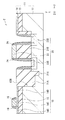
- FIG. 2 is a schematic diagram illustrating a cross-sectional configuration of the semiconductor device according to the first embodiment of the present disclosure.
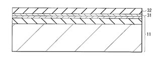
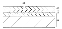
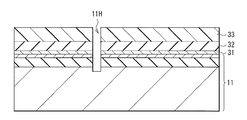
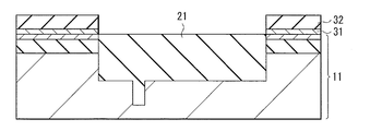
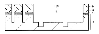
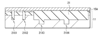
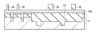
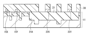
- FIG. It is a cross-sectional schematic diagram for demonstrating the manufacturing method of the manufacturing method of the semiconductor device shown in FIG. It is a cross-sectional schematic diagram showing the process following FIG. 2A. It is a cross-sectional schematic diagram showing the process following FIG. 2B. It is a cross-sectional schematic diagram showing the process following FIG. 2C. It is a cross-sectional schematic diagram showing the process following FIG. 2D. It is a cross-sectional schematic diagram showing the process following FIG. 3A. It is a cross-sectional schematic diagram showing the process following FIG. 3B. It is a cross-sectional schematic diagram showing the process following FIG. 3C.
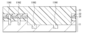
- FIG. 4A It is a cross-sectional schematic diagram showing the process following FIG. 4A. It is a cross-sectional schematic diagram showing the process following FIG. 4B. It is a cross-sectional schematic diagram showing the process following FIG. 4C. It is a cross-sectional schematic diagram showing the process following FIG. 5A. It is a cross-sectional schematic diagram showing the process following FIG. 5B. It is a cross-sectional schematic diagram showing the process following FIG. 5C. It is a cross-sectional schematic diagram showing the process following FIG. 6A. It is a cross-sectional schematic view illustrating a thickening of the common SiO 2 film. It is a cross-sectional schematic diagram showing the process following FIG. 7A.
- FIG. 7B It is a cross-sectional schematic diagram showing the process of following FIG. 7B. It is a cross-sectional schematic diagram for demonstrating the manufacturing method of the semiconductor device which concerns on 2nd Embodiment of this indication. It is a cross-sectional schematic diagram showing the process following FIG. 8A. It is a cross-sectional schematic diagram showing the process of following FIG. 8B. It is a cross-sectional schematic diagram showing the process of following FIG. 8C. It is a schematic diagram showing the cross-sectional structure of the semiconductor device which concerns on the modification 1 of this indication. It is a cross-sectional schematic diagram for demonstrating the manufacturing method of the semiconductor device which concerns on the modification 2 of this indication. It is a cross-sectional schematic diagram showing the process following FIG. 10A.
- FIG. 10B It is a cross-sectional schematic diagram showing the process following FIG. 10B. It is a cross-sectional schematic diagram showing the process following FIG. 10C. It is a cross-sectional schematic diagram showing the process of following FIG. 11A. It is a cross-sectional schematic diagram showing the process of following FIG. 11B. It is a cross-sectional schematic diagram showing the process of following FIG. 11C. It is a cross-sectional schematic diagram showing the process following FIG. 12A. It is a cross-sectional schematic diagram showing the process of following FIG. 12B. It is a cross-sectional schematic diagram showing the process of following FIG. 12C. It is a cross-sectional schematic diagram showing the process of following FIG. 13A.
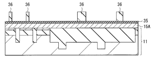
- FIG. 13B It is a cross-sectional schematic diagram showing the process of following FIG. 13B. It is a cross-sectional schematic diagram showing the process of following FIG. 13C. It is a cross-sectional schematic diagram showing the process following FIG. 14A. It is a cross-sectional schematic diagram showing the process of following FIG. 14B. It is a cross-sectional schematic diagram for demonstrating the manufacturing method of the semiconductor device which concerns on the modification 3 of this indication. It is a cross-sectional schematic diagram showing the process following FIG. 15A. It is a cross-sectional schematic diagram showing the process of following FIG. 15B. It is a cross-sectional schematic diagram showing the process of following FIG. 15C. It is a cross-sectional schematic diagram showing the process following FIG. 16A.
- First Embodiment Example in which an element isolation film having a thickness larger than that of a BOX layer is formed and a part thereof is used as a gate insulating film of a high voltage transistor
- Configuration of semiconductor device 1-2 Manufacturing method of semiconductor device 1-3.
- Action / Effect Second embodiment example of forming a gate electrode only with a resist film
- Modified example 3-1 Modification 1 (example in which openings having different depths are provided in the element isolation film portion and the gate insulating film portion) 3-2.
- Modification 2 Modification of the first embodiment) 3-3.
- Modification 3 Modification of the second embodiment 4).
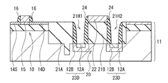
- FIG. 1 illustrates a cross-sectional configuration of a semiconductor device (semiconductor device 1) according to the first embodiment of the present disclosure.
- the semiconductor device 1 has transistors (first transistor and second transistor) having different withstand voltages on the same substrate.
- transistors first transistor and second transistor
- SPAD Single Photon Avalanche Diode
- the semiconductor device 1 is a device in which, for example, a leading-edge transistor (transistor 10) of the 22 nm generation or later and a transistor (transistor 20) capable of receiving a high voltage of, for example, several tens of volts or more are mounted on the SOI substrate 11.
- the SOI substrate 11 is formed by laminating a silicon substrate layer 12, an insulating layer 13 (first insulating layer), and a semiconductor layer 14 in this order.
- the transistor 10 is provided on the semiconductor layer 14 constituting the SOI substrate 11
- the transistor 20 is provided on the silicon substrate layer 12 constituting the SOI substrate 11.
- an element isolation film 21A having a thickness in the Y-axis direction (hereinafter simply referred to as thickness) greater than that of the insulating layer 13 is provided, and the insulating layer constituting the element isolation film 21A 21 (for example, refer to FIG. 3C) has a configuration in which a part of the gate insulating film 21B of the transistor 20 is used.
- the semiconductor device 1 is provided on the SOI substrate 11 with the element isolation film 21 ⁇ / b> A between the transistor 10, which is a front-end transistor, and the transistor 20 that can receive a high voltage of, for example, several tens of volts or more. It has a configuration.
- the SOI substrate 11 is obtained by laminating an insulating layer 13 and a semiconductor layer 14 in this order on a silicon substrate layer 12 made of bulk silicon.
- the insulating layer 13 is a so-called BOX layer, and is composed of, for example, a silicon oxide film (SiO 2 film) of 20 nm or less.
- the semiconductor layer 14 is composed of, for example, a silicon single crystal layer of 6 nm or less.
- the transistor 10 is a leading-edge transistor after the 22 nm generation, for example, a fully depleted silicon-on-insulator (FD-SOI) transistor.
- the transistor 10 has a planar type transistor structure.
- the transistor 10 has a gate electrode 15 on the semiconductor layer 14.
- a gate insulating film made of, for example, hafnium oxide (HfO 2 ) or the like is provided between the gate electrode 15 and the semiconductor layer 14.
- a side wall 16 made of, for example, a silicon nitride film is provided on the side surface of the gate electrode 15.
- a channel region 14 ⁇ / b> C is provided in the semiconductor layer 14 facing the gate electrode 15.
- a source region 14S and a drain region 14D formed by diffusing impurities are provided on both sides of the channel region 14C.
- the transistor 10 is an NMOS transistor
- phosphorus (P) having an ion implantation dose of 1E18 to 19 / cm 2 is diffused into the source region 14S and the drain region 14D, for example.
- boron (B) of, for example, 1E18 to 19 / cm 2 is diffused into the source region 14S and the drain region 14D.
- the transistor 20 is a so-called high breakdown voltage transistor that can receive a high voltage of, for example, a few dozen V to 20 V or more.
- the transistor 20 is a silicon planar type transistor, for example, between the gate electrode 22, the source region 23 ⁇ / b> S and the drain region 23 ⁇ / b> D provided on the silicon substrate layer 12, and the silicon substrate layer 12 and the gate electrode 22. And a provided gate insulating film 21B.
- the gate electrode 22 is provided on the silicon substrate layer 12.
- the gate insulating film 21B is provided between the gate electrode 22 and the silicon substrate layer 12 as described above.
- the gate insulating film 21B is made of, for example, a SiO 2 film, and the thickness (W2) thereof is larger than the thickness (W1) of the BOX layer (insulating layer 13) of the SOI substrate 11.
- a side wall 24 made of, for example, silicon nitride is provided on the side surface of the gate electrode 22.
- the sidewall 24 is provided on the silicon substrate layer 12 and is formed continuously on the side surfaces of the gate electrode 22 and the gate insulating film 21B.
- the source region 23S and the drain region 23D are formed by diffusing impurities into the silicon substrate layer 12 on both sides of the channel region facing the gate electrode 22.
- the source region 23S and the drain region 23D are provided, for example, around the high-concentration diffusion region 12A having a high impurity diffusion concentration and the high-concentration diffusion region 12A, and having a lower impurity concentration than the high-concentration diffusion region 12A. It is composed of a diffusion region 12B.
- the high concentration diffusion region 12A and the low concentration diffusion region 12B have the following configurations, for example.
- the transistor 20 when the transistor 20 is an NMOS transistor, phosphorus (P) having, for example, an ion implantation dose of 1E17 to 18 / cm 2 is diffused in the high concentration diffusion region 12A, and the low concentration diffusion region 12B includes For example, phosphorus (P) of 1E14 to 15 / cm 2 is diffused.
- the transistor 20 when the transistor 20 is a PMOS transistor, for example, boron (B) of 1E17 to 18 / cm 2 is diffused in the high concentration diffusion region 12A, and the low concentration diffusion region 12B includes, for example, Boron (B) of 1E14-15 / cm 2 is diffused.
- the element isolation film 21 ⁇ / b > A is made of, for example, SiO 2 provided between the transistor 10 and the transistor 20.
- the element isolation film 21 ⁇ / b> A is thicker than the BOX layer (insulating layer 13) of the SOI substrate 11.
- the element isolation film 21A will be described in detail later.
- the element isolation film 21A penetrates the semiconductor layer 14 and the insulating layer 13 of the SOI substrate 11 and has a bottom surface embedded in the opening 12H existing in the silicon substrate layer 12 (first layer). 2 insulating layers).
- a convex portion 21 ⁇ / b> X that protrudes from the silicon substrate layer 12 is provided on a part of the bottom surface of the element isolation film 21 ⁇ / b> A.
- the convex portion 21X is not necessarily provided when the front end transistor (transistor 10) and the high breakdown voltage transistor (transistor 20) are disposed sufficiently apart (for example, 10 ⁇ m or more). However, for example, when a plurality of high-end transistors and high-breakdown-voltage transistors are provided on the SOI substrate and a plurality of high-breakdown-voltage transistors (transistors 20) are arranged adjacent to each other, the protrusion 21X is formed on the bottom surface of the element isolation film 21A provided therebetween. Is preferably provided. As a result, the insulation between the high breakdown voltage transistors is improved, the distance between the high breakdown voltage transistors can be arranged close to 1 ⁇ m, for example, and the chip area can be reduced.
- the insulating layer 21 is divided by an opening 21H1 and an opening 21H2, and the insulating layer 21 divided by the opening 21H constitutes an element isolation film 21A. Further, the insulating layer 21 divided by the opening 21H1 and the opening 21H2 constitutes the gate insulating film 21B of the transistor 20.
- the insulating layer 21 is divided into three by the opening 21H1 and the opening 21H2 is shown, but the present invention is not limited to this. For example, it may be divided into two by the opening 21H1, and one may be used as the element isolation film 21A and the other as the gate insulating film 21B.
- the remaining insulating layer 21 is arranged adjacent to each other by dividing into three as in the present embodiment. It can be used as an element isolation film with a transistor.
- the semiconductor device 1 of the present embodiment can be manufactured, for example, as follows.
- an SOI substrate 11 in which a silicon substrate layer 12, an insulating layer 13, and a semiconductor layer 14 are stacked in this order is prepared.
- an oxide film 31 of, for example, 1 nm is formed on the SOI substrate 11 (specifically, the surface of the semiconductor layer 14) by, for example, thermal oxidation, and then on the oxide film 31.
- a silicon nitride film (SiN film) 32 of 30 nm, for example, is formed by using LPCVD (Low Pressure Chemical Vapor Deposition) method.
- a resist film 33 is formed on the SiN film 32 and then patterned to form an opening 33H.
- an opening 11H reaching the silicon substrate layer 12 to be the convex portion 21X is formed by, for example, an etching method.
- the resist film 34 having the opening 34H including the opening 11H is patterned on the SiN film 32.
- an opening 12H reaching the silicon substrate layer 12 is formed by, for example, an etching method.
- FIG. 3C after removing the resist film 34, for example, using a high-density plasma chemical vapor deposition (HDP-CVD) method, the silicon oxide film (SiO 2 film, An insulating layer 21) is buried. Subsequently, the surface of the insulating layer 21 is planarized by, for example, CMP (Chemical Mechanical Polishing).
- CMP Chemical Mechanical Polishing
- the insulating layer 21 is etched to adjust to an arbitrary thickness using, for example, a wet etching method.
- etching is performed to a thickness that forms the same surface as the semiconductor layer 14.
- FIG. 4B after the SiN film 32 and the oxide film 31 are removed, for example, a hafnium oxide film that becomes a gate insulating film of the transistor 10 is formed on the entire surface of the SOI substrate 11, for example.
- a film (HfO 2 film) is formed with a thickness of 2 nm, for example.
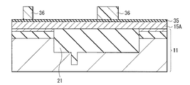
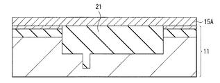
- a polysilicon (Si) film 15A is formed on the semiconductor layer 14 and the insulating layer 21 (actually on the HfO 2 film) of the SOI substrate 11 by using, for example, a CVD method. Film.
- the HfO 2 film may be patterned only in the formation region of the transistor 10, but the presence or absence of the HfO 2 film does not particularly affect the characteristics of the transistor 20. It may be formed on the entire surface of the SOI substrate 11.
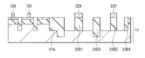
- a resist film 36 is patterned on the SiN film 35.
- the SiN film 35 and the poly-Si film 15A are etched by, for example, an etching method.
- the gate electrodes 15 and 22 of the transistor 10 and the transistor 20 are collectively formed on the HfO 2 film.
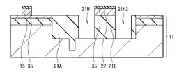
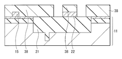
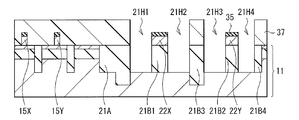
- a resist film 37 having an opening including the gate electrode 22 of the transistor 20 is patterned on the SOI substrate 11.
- the insulating layer 21 in the opening of the resist film 37 is etched using, for example, an etching method.
- the SiN film 35 on the gate electrode 22 serves as an etching mask, and an opening 21H1 and an opening 21H2 are formed in the insulating layer 21.
- the insulating layer 21 is divided into three, the insulating layer 21 below the gate electrode 22 becomes the gate insulating film 21B of the transistor 20, and the insulating layer 21 divided on the transistor 10 side is the transistor 10 and the transistor 20
- an element isolation film 21A for electrically isolating the two is obtained.
- the resist film 37 is removed.
- a low concentration diffusion region 12B is formed in the silicon substrate layer 12 by using, for example, an ion implantation method.
- a SiN film is formed using, for example, a CVD method, and then etched back to perform sidewalls 16 on the side surfaces of the gate electrode 15 of the transistor 10 and the side surfaces of the gate electrode 22 of the transistor 20 and the gate insulating film 21B. , 24 are formed.
- SiN films having the same shape as the sidewalls 24 are also formed on the side surfaces of the element isolation films 21A constituting the openings 21H1 and 21H2 and the side surfaces of the insulating layer 21 on the opposite side across the gate insulating film 21B.
- a high concentration diffusion region 12A is formed in the silicon substrate layer 12 in the openings 21H1 and 21H2 by using, for example, an ion implantation method.
- the SiN film formed on the side surface of the side wall 24 and the element isolation film 21A and the side surface of the insulating layer 21 opposite to the gate insulating film 21B is used as a mask, and the high concentration diffusion region 12A is It is formed inside the formed low concentration diffusion region 12B. Thereby, the semiconductor device 1 shown in FIG. 1 is completed.
- the semiconductor device 1 of this Embodiment is used for a ranging image sensor etc. as mentioned above.
- the pixel unit 50 including the photoelectric conversion unit is disposed on the semiconductor device 1 illustrated in FIG. 1.
- a plurality of unit pixels P are arranged on a matrix.
- the transistor 10 and the transistor 20 are provided in each unit pixel P.
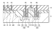
- an interlayer insulating layer 41 made of, for example, a silicon oxide film or a silicon oxide film containing phosphorus or boron is formed on the semiconductor device 1 by using, for example, a CVD method.
- the contact plugs P1, P2, P3, P4, P5, and P6 are formed in the interlayer insulating layer 41. As shown in FIG. 6B, one end of each of the contact plugs P1, P2, P3, P4, P5, and P6 is a gate electrode 15, a source region 14S and a drain region 14D of the transistor 10, a gate electrode 22 of the transistor 20, and a source region, respectively. 23S and drain region 23D are electrically connected. The other end is connected to a predetermined part of the unit pixel P.
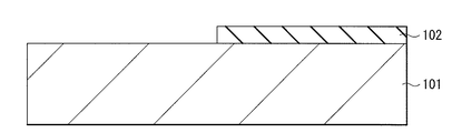
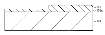
- the gate insulating films of the low-voltage operation transistor and the high-voltage operation transistor are separately formed using a multi-oxide process. Specifically, first, as shown in FIG. 7A, the silicon substrate 101 is thickly oxidized to form the SiO 2 film 102, and then, as shown in FIG. 7B, a predetermined region (for example, a low-voltage operation transistor is formed). The SiO 2 film 102 in the region to be formed is removed. After that, as shown in FIG. 7C, the silicon substrate 101 is thin-film oxidized to form SiO 2 films 102 having different thicknesses on the silicon substrate 101.
- a leading-edge transistor for example, FD-SOI transistor
- a transistor high voltage transistor capable of receiving a high voltage of several tens of volts or more.
- the FD-SOI transistor is formed on an SOI substrate in which a thin Si layer is provided on a silicon substrate via an insulating layer (BOX layer).
- BOX layer insulating layer
- the gate insulating film is required to have a thickness of, for example, 50 nm or more from the viewpoint of reliability.
- a BOX layer of about 20 nm has a high breakdown voltage transistor.
- the withstand voltage is insufficient. Therefore, it is conceivable to increase the thickness of the BOX layer (for example, about 50 nm), but in this case, the back bias control performed in the FD-SOI transistor cannot be performed.
- an opening 12H that penetrates through the semiconductor layer 14 and the insulating layer 13 constituting the SOI substrate 11 and reaches the silicon substrate layer 12 is formed in the SOI substrate 11 as the element isolation film 21A.
- the insulating layer 21 was embedded, and a part thereof was used as the gate insulating film 21B of the high voltage transistor (transistor 20).
- the thickness of the insulating layer 21 can be arbitrarily set by adjusting the depth of the opening 12H. As a result, the thickness of the gate insulating film 21B of the high breakdown voltage transistor 20 can be sufficiently ensured without affecting the operation of the transistor 10 which is the advanced transistor and the manufacturing process.
- An isolation film 21A is provided, and a part of the insulating layer 21 constituting the element isolation film 21A is used as a gate insulating film of the transistor 20.
- an opening 12H that penetrates the semiconductor layer 14 and the insulating layer 13 and reaches the silicon substrate layer 12 is provided in the SOI substrate 11, and the opening 12H is embedded in the insulating layer 21, and the insulating layer 21 is divided.
- the gate insulating film 21B having sufficient withstand voltage performance is formed as the gate insulating film of the transistor 20 which is a high breakdown voltage transistor. Therefore, it is possible to provide the semiconductor device 1 having transistors with different breakdown voltages on the same substrate and having high reliability.
- the projecting portion 21X protruding from the silicon substrate layer 12 is provided on the bottom surface of the element isolation film 21A, the electrical insulation between the transistor 10 and the transistor 20 is improved, and the transistor 10 and the transistor 20 It is possible to reduce the distance to When a plurality of transistors 20 are arranged adjacent to each other, the distance between the transistors 20 can be reduced by providing the convex portion 21X between them. Therefore, the chip area can be reduced.
- Second Embodiment> 8A to 8B schematically show another example of the method for manufacturing the semiconductor device 1 according to the second embodiment of the present disclosure.
- a poly-Si film 15A is formed on the SOI substrate 11 and then shown in FIG. 8B.
- the resist film 36 is patterned on the Si film 15 ⁇ / b> A without forming the SiN film 35.
- the poly-Si film 15A is etched using the resist film 36 as a mask to form the gate electrode 15 of the transistor 10 and the gate electrode 22 of the transistor 20. Thereafter, the resist film 36 is removed.
- the insulating layer 21 is formed by using the same method as in the first embodiment. Etch. Thereby, the opening 21H1 and the opening 21H2 are formed in the insulating layer 21, and the insulating layer 21 is divided into three. Thereafter, the semiconductor device 1 shown in FIG. 1 is completed by using the same method as in the first embodiment.
- the semiconductor device 1 is formed without forming the SiN film 35 that serves as a mask for etching the insulating layer 21 that forms the openings 21H1 and 21H2. Thereby, compared with the manufacturing method of the semiconductor device 1 in the first embodiment, the number of manufacturing steps can be reduced.
- FIG. 9 illustrates a cross-sectional configuration of a semiconductor device (semiconductor device 2) according to Modification 1 of the present disclosure.
- the semiconductor device 2 of the present modification is formed by forming an opening 12H having a plurality of depths (here, three types) and an insulating layer 21 having a step on the bottom surface.
- the element isolation film 21A is thicker than the gate insulating film 21B with the convex portion 21X described in the first embodiment interposed therebetween.
- the thicknesses of the element isolation film 21A and the gate insulating film 21B can be adjusted as appropriate.
- FIG. 14C show a method for manufacturing a semiconductor device (semiconductor device 3, see FIG. 14C) as a modification of the first embodiment.
- a semiconductor device 3 of this modification a plurality of transistors 10 and transistors 20 are provided on the SOI substrate 11 (two transistors 10X and 10Y and transistors 20X and 20Y, respectively, in this modification).
- Such a semiconductor device 3 can be manufactured as follows, for example.
- the oxide film 31 and the SiN film 32 are formed on the SOI substrate 11 by using the same method as in the first embodiment.
- a resist film 33 is formed on the SiN film 32 and then patterned to form, for example, four openings 33H1 to 33H4.
- openings 11H1 to 11H4 reaching the silicon substrate layer 12 are formed by, eg, etching.
- a resist film 34 having openings in the formation regions 20R of the transistors 20X and 20Y is patterned on the SiN film 32 as shown in FIG. 10C.
- an opening 12H reaching the silicon substrate layer 12 is formed by, for example, an etching method.
- removing the resist film 34 as shown in FIG. 11B, for example, in the openings 11H1 and 11H2 and the openings 12H including the openings 11H3 and 11H4 and on the SiN film 32 using, for example, the HDP-CVD method.
- a SiO 2 film (insulating layer 21) is formed.
- the surface of the insulating layer 21 is planarized by, eg, CMP.
- convex portions 21X1, 21X2, 21X3, and 21X4 that electrically insulate the transistors 10X and 10Y and the transistors 20X and 20Y that are finally disposed adjacent to each other are formed.
- the SiN film 32 and the oxide film 31 are removed.
- an HfO 2 film for example, serving as a gate insulating film of the transistor 10 is formed on the entire surface of the SOI substrate 11 with a thickness of, for example, 2 nm.
- the polysilicon (Si) film 15A and the SiN film 35 are formed in this order by using, for example, the CVD method.
- a resist film 36 is patterned on the SiN film 35.
- the SiN film 35 and the poly-Si film 15A are etched by the etching method, for example, using the resist film 36 as a mask.
- the gate electrodes 15X, 15Y, 22X, and 22Y of the transistors 10X and 10Y and the transistors 20X and 20Y are collectively formed.
- a resist film 37 is patterned on the semiconductor layer 14 and the insulating layer 21 of the SOI substrate 11, as shown in FIG. 13B.
- the insulating layer 21 is etched using, for example, an etching method.
- the SiN film 35 on the gate electrode 22 together with the resist film 37 serves as an etching mask, and openings 21H1, 21H2, 21H3, and 21H4 are formed.
- the insulating layer 21 in the opening 12H is divided into five parts.
- An element isolation film (insulating film 21B3) that electrically insulates between 20X and transistor 20Y and, for example, element isolation when another transistor is formed on the opposite side of transistor 20Y from transistor 20X (not shown)
- a film (insulating film 21B4) is formed.
- the SiN film 35 provided on the resist film 37 and the gate electrodes 15X, 15Y, 22X, and 22Y is removed.
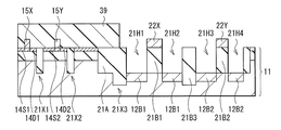
- source regions 14S1 and 14S2 and drain regions 14D1 and 14D2 are formed in the semiconductor layer 14 on both sides of the transistors 10X and 10Y by using, for example, an ion implantation method.
- a resist film 39 is formed on the semiconductor layer 14 including the transistors 10X and 10Y and on the element isolation film 21A.
- low-concentration diffusion regions 12B1 and 12B2 are formed in the silicon substrate layer 12 in the openings 21H1 and 21H2 and the openings 21H3 and 21H4 by using, for example, an ion implantation method.
- FIG. 14A source regions 14S1 and 14S2 and drain regions 14D1 and 14D2 are formed in the semiconductor layer 14 on both sides of the transistors 10X and 10Y by using, for example, an ion implantation method.
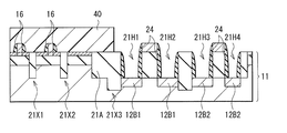
- a SiN film is formed by using, for example, a CVD method, and etching back is performed to form side surfaces of the gate electrodes 15X and 15Y of the transistors 10X and 10Y.
- Side walls 16 and 24 are formed on the side surfaces of the transistors 20X and 20Y that are continuous with the gate electrode 22X and the gate insulating film 21B1, and the gate electrode 22Y and the gate insulating film 21B2, respectively.
- SiN films having the same shape as the sidewalls are also formed on the side surfaces of the element isolation film 21A and the insulating films 21B3 and 21B4 which are element isolation films between the transistors.
- a resist film 40 is formed again on the semiconductor layer 14 including the transistors 10X and 10Y and the element isolation film 21A.
- the high concentration diffusion regions 12A1 and 12A2 are formed in the silicon substrate layer 12 in the openings 21H1, 21H2, 21H3, and 21H4 by using, for example, an ion implantation method.
- the side wall 24 and the SiN film formed on the side surfaces of the element isolation film 21A and the insulating films 21B3 and 21B4 are used as a mask, and the high concentration diffusion regions 12A1 and 12A2 are formed in the low concentration diffusion regions previously formed. It is formed inside 12B1 and 12B2.
- the two convex portions 21X2 and 21X3 are provided between the transistor 10Y and the transistor 20X is shown, but between the leading transistor (transistor 10Y) and the high breakdown voltage transistor (transistor 20X),
- the protrusion 21X2 may be omitted as long as the protrusion 21X3 having a deeper tip at least is formed.
- (3-3. Modification 3) 15A to 16B show a method for manufacturing the semiconductor device 3 as a modification of the second embodiment.
- the semiconductor device 3 can be manufactured as follows, for example.
- the convex portions 21X1, 21X2, 21X3, and 21X4 are formed by using the same method as in the first modification, and then, as shown in FIG. 15A, on the semiconductor layer 14 and the insulating layer 21 of the SOI substrate 11 (actually A polysilicon (Si) film 15A is formed on the HfO 2 film by using, for example, a CVD method. Subsequently, as shown in FIG. 15B, a resist film 36 is patterned on the Si film 15A. Subsequently, as shown in FIG.
- the poly-Si film 15A is etched using the resist film 36 as a mask to form the gate electrodes 15X and 15Y of the transistors 10X and 10Y and the gate electrodes 22X and 22Y of the transistors 20X and 20Y, respectively. To do.
- the resist film 38 is patterned on the semiconductor layer 14 and the insulating layer 21 of the SOI substrate 11, and then the insulating layer 21 is formed by using the same method as in the first embodiment. Etching is performed to form openings 21H1, 21H2, 21H3, and 21H4 as shown in FIG. 16B. Thereafter, the semiconductor device 3 shown in FIG. 14C is completed by using the same method as in the first modification.
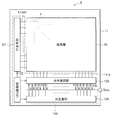
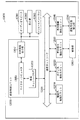
- FIG. 17 shows the entire imaging device (imaging device 4) using the imaging device including the semiconductor device (semiconductor devices 1 and 2) shown in the first embodiment (or modification) for each unit pixel P. It represents the configuration.
- the imaging device 4 is a CMOS image sensor, and has, for example, a pixel unit 50 as an imaging area on the SOI substrate 11 and, for example, a row scanning unit 131 and a horizontal selection unit in a peripheral region of the pixel unit 50.
- 133, a peripheral circuit unit 130 including a column scanning unit 134 and a system control unit 132 is provided.
- the pixel unit 50 includes, for example, a plurality of unit pixels P (corresponding to an image sensor) that are two-dimensionally arranged in a matrix.
- a pixel drive line Lread (specifically, a row selection line and a reset control line) is wired for each pixel row, and a vertical signal line Lsig is wired for each pixel column.
- the pixel drive line Lread transmits a drive signal for reading a signal from the pixel.
- One end of the pixel drive line Lread is connected to an output end corresponding to each row of the row scanning unit 131.
- the row scanning unit 131 is configured by a shift register, an address decoder, or the like, and is a pixel driving unit that drives each unit pixel P of the pixel unit 50 in units of rows, for example.
- a signal output from each unit pixel P of the pixel row that is selectively scanned by the row scanning unit 131 is supplied to the horizontal selection unit 133 through each of the vertical signal lines Lsig.
- the horizontal selection unit 133 is configured by an amplifier, a horizontal selection switch, and the like provided for each vertical signal line Lsig.
- the column scanning unit 134 includes a shift register, an address decoder, and the like, and drives the horizontal selection switches in the horizontal selection unit 133 in order while scanning. By the selective scanning by the column scanning unit 134, the signal of each pixel transmitted through each of the vertical signal lines Lsig is sequentially output to the horizontal signal line 135 and transmitted to the outside of the SOI substrate 11 through the horizontal signal line 135. .
- the circuit portion including the row scanning unit 131, the horizontal selection unit 133, the column scanning unit 134, and the horizontal signal line 135 may be formed directly on the SOI substrate 11 or provided in the external control IC. It may be. In addition, these circuit portions may be formed on another substrate connected by a cable or the like.
- the system control unit 132 receives a clock given from the outside of the SOI substrate 11, data for instructing an operation mode, and the like, and outputs data such as internal information of the imaging device 4.
- the system control unit 132 further includes a timing generator that generates various timing signals, and the row scanning unit 131, the horizontal selection unit 133, the column scanning unit 134, and the like based on the various timing signals generated by the timing generator. Peripheral circuit drive control.
- the imaging device 4 can be applied to all types of electronic devices having an imaging function, such as a camera system such as a digital still camera or a video camera, or a mobile phone having an imaging function.
- FIG. 18 shows a schematic configuration of an electronic device 5 (camera) as an example.
- the electronic device 5 is, for example, a video camera capable of taking a still image or a moving image, and drives the imaging device 4, an optical system (optical lens) 310, a shutter device 311, the imaging device 4 and the shutter device 311.
- a driving unit 313 and a signal processing unit 312 are included.
- the optical system 310 guides image light (incident light) from a subject to the pixel unit 50 of the imaging device 4.
- the optical system 310 may be composed of a plurality of optical lenses.
- the shutter device 311 controls the light irradiation period and the light shielding period to the imaging device 4.
- the drive unit 313 controls the transfer operation of the imaging device 4 and the shutter operation of the shutter device 311.
- the signal processing unit 312 performs various signal processing on the signal output from the imaging device 4.
- the video signal Dout after the signal processing is stored in a storage medium such as a memory, or is output to a monitor or the like.
- the imaging device 4 can also be applied to the following electronic devices (capsule endoscope 10100 and moving bodies such as vehicles).
- FIG. 19 is a block diagram illustrating an example of a schematic configuration of an in-vivo information acquisition system for a patient using a capsule endoscope to which the technology according to the present disclosure (present technology) can be applied.
- the in-vivo information acquisition system 10001 includes a capsule endoscope 10100 and an external control device 10200.
- the capsule endoscope 10100 is swallowed by the patient at the time of examination.
- the capsule endoscope 10100 has an imaging function and a wireless communication function, and moves inside the organ such as the stomach and intestine by peristaltic motion or the like until it is spontaneously discharged from the patient.
- Images (hereinafter also referred to as in-vivo images) are sequentially captured at predetermined intervals, and information about the in-vivo images is sequentially wirelessly transmitted to the external control device 10200 outside the body.
- the external control device 10200 comprehensively controls the operation of the in-vivo information acquisition system 10001. Further, the external control device 10200 receives information about the in-vivo image transmitted from the capsule endoscope 10100 and, based on the received information about the in-vivo image, displays the in-vivo image on the display device (not shown). The image data for displaying is generated.
- an in-vivo image obtained by imaging the inside of the patient's body can be obtained at any time in this manner until the capsule endoscope 10100 is swallowed and discharged.
- the capsule endoscope 10100 includes a capsule-type casing 10101.
- a light source unit 10111 In the casing 10101, a light source unit 10111, an imaging unit 10112, an image processing unit 10113, a wireless communication unit 10114, a power supply unit 10115, and a power supply unit 10116 and the control unit 10117 are housed.
- the light source unit 10111 includes a light source such as an LED (light-emitting diode), and irradiates the imaging field of the imaging unit 10112 with light.
- a light source such as an LED (light-emitting diode)
- the imaging unit 10112 includes an imaging device and an optical system including a plurality of lenses provided in front of the imaging device. Reflected light (hereinafter referred to as observation light) of light irradiated on the body tissue to be observed is collected by the optical system and enters the image sensor. In the imaging unit 10112, in the imaging element, the observation light incident thereon is photoelectrically converted, and an image signal corresponding to the observation light is generated. The image signal generated by the imaging unit 10112 is provided to the image processing unit 10113.
- the image processing unit 10113 is configured by a processor such as a CPU (Central Processing Unit) or a GPU (Graphics Processing Unit), and performs various types of signal processing on the image signal generated by the imaging unit 10112.
- the image processing unit 10113 provides the radio communication unit 10114 with the image signal subjected to signal processing as RAW data.
- the wireless communication unit 10114 performs predetermined processing such as modulation processing on the image signal that has been subjected to signal processing by the image processing unit 10113, and transmits the image signal to the external control apparatus 10200 via the antenna 10114A.
- the wireless communication unit 10114 receives a control signal related to drive control of the capsule endoscope 10100 from the external control device 10200 via the antenna 10114A.
- the wireless communication unit 10114 provides a control signal received from the external control device 10200 to the control unit 10117.
- the power feeding unit 10115 includes a power receiving antenna coil, a power regeneration circuit that regenerates power from a current generated in the antenna coil, a booster circuit, and the like. In the power feeding unit 10115, electric power is generated using a so-called non-contact charging principle.
- the power supply unit 10116 is composed of a secondary battery, and stores the electric power generated by the power supply unit 10115.
- FIG. 19 in order to avoid complication of the drawing, illustration of an arrow or the like indicating a power supply destination from the power supply unit 10116 is omitted, but the power stored in the power supply unit 10116 is stored in the light source unit 10111.
- the image pickup unit 10112, the image processing unit 10113, the wireless communication unit 10114, and the control unit 10117 can be used for driving them.
- the control unit 10117 includes a processor such as a CPU, and a control signal transmitted from the external control device 10200 to drive the light source unit 10111, the imaging unit 10112, the image processing unit 10113, the wireless communication unit 10114, and the power feeding unit 10115. Control accordingly.
- a processor such as a CPU
- the external control device 10200 is configured by a processor such as a CPU or GPU, or a microcomputer or a control board in which a processor and a storage element such as a memory are mounted.
- the external control device 10200 controls the operation of the capsule endoscope 10100 by transmitting a control signal to the control unit 10117 of the capsule endoscope 10100 via the antenna 10200A.
- the capsule endoscope 10100 for example, the light irradiation condition for the observation target in the light source unit 10111 can be changed by a control signal from the external control device 10200.
- an imaging condition for example, a frame rate or an exposure value in the imaging unit 10112
- a control signal from the external control device 10200 can be changed by a control signal from the external control device 10200.
- the contents of processing in the image processing unit 10113 and the conditions (for example, the transmission interval, the number of transmission images, etc.) by which the wireless communication unit 10114 transmits an image signal may be changed by a control signal from the external control device 10200. .
- the external control device 10200 performs various image processing on the image signal transmitted from the capsule endoscope 10100, and generates image data for displaying the captured in-vivo image on the display device.
- image processing for example, development processing (demosaic processing), image quality enhancement processing (band enhancement processing, super-resolution processing, NR (Noise reduction) processing and / or camera shake correction processing, etc.), and / or enlargement processing ( Various signal processing such as electronic zoom processing can be performed.
- the external control device 10200 controls driving of the display device to display an in-vivo image captured based on the generated image data.
- the external control device 10200 may cause the generated image data to be recorded on a recording device (not shown) or may be printed out on a printing device (not shown).
- the technology according to the present disclosure can be applied to, for example, the imaging unit 10112 among the configurations described above. Thereby, since a fine operation part image can be obtained, the accuracy of examination improves.
- the technology according to the present disclosure can be applied to various products.
- the technology according to the present disclosure is realized as a device that is mounted on any type of mobile body such as an automobile, an electric vehicle, a hybrid electric vehicle, a motorcycle, a bicycle, personal mobility, an airplane, a drone, a ship, and a robot. May be.
- FIG. 20 is a block diagram illustrating a schematic configuration example of a vehicle control system that is an example of a mobile control system to which the technology according to the present disclosure can be applied.
- the vehicle control system 12000 includes a plurality of electronic control units connected via a communication network 12001.
- the vehicle control system 12000 includes a drive system control unit 12010, a body system control unit 12020, a vehicle exterior information detection unit 12030, a vehicle interior information detection unit 12040, and an integrated control unit 12050.
- a microcomputer 12051, an audio image output unit 12052, and an in-vehicle network I / F (interface) 12053 are illustrated as a functional configuration of the integrated control unit 12050.
- the drive system control unit 12010 controls the operation of the device related to the drive system of the vehicle according to various programs.
- the drive system control unit 12010 includes a driving force generator for generating a driving force of a vehicle such as an internal combustion engine or a driving motor, a driving force transmission mechanism for transmitting the driving force to wheels, and a steering angle of the vehicle. It functions as a control device such as a steering mechanism that adjusts and a braking device that generates a braking force of the vehicle.
- the body system control unit 12020 controls the operation of various devices mounted on the vehicle body according to various programs.
- the body system control unit 12020 functions as a keyless entry system, a smart key system, a power window device, or a control device for various lamps such as a headlamp, a back lamp, a brake lamp, a blinker, or a fog lamp.
- the body control unit 12020 can be input with radio waves transmitted from a portable device that substitutes for a key or signals from various switches.
- the body system control unit 12020 receives input of these radio waves or signals, and controls a door lock device, a power window device, a lamp, and the like of the vehicle.
- the vehicle outside information detection unit 12030 detects information outside the vehicle on which the vehicle control system 12000 is mounted.
- the imaging unit 12031 is connected to the vehicle exterior information detection unit 12030.
- the vehicle exterior information detection unit 12030 causes the imaging unit 12031 to capture an image outside the vehicle and receives the captured image.
- the vehicle outside information detection unit 12030 may perform an object detection process or a distance detection process such as a person, a car, an obstacle, a sign, or a character on a road surface based on the received image.
- the imaging unit 12031 is an optical sensor that receives light and outputs an electrical signal corresponding to the amount of received light.
- the imaging unit 12031 can output an electrical signal as an image, or can output it as distance measurement information. Further, the light received by the imaging unit 12031 may be visible light or invisible light such as infrared rays.
- the vehicle interior information detection unit 12040 detects vehicle interior information.
- a driver state detection unit 12041 that detects a driver's state is connected to the in-vehicle information detection unit 12040.
- the driver state detection unit 12041 includes, for example, a camera that images the driver, and the vehicle interior information detection unit 12040 determines the degree of fatigue or concentration of the driver based on the detection information input from the driver state detection unit 12041. It may be calculated or it may be determined whether the driver is asleep.
- the microcomputer 12051 calculates a control target value of the driving force generator, the steering mechanism, or the braking device based on the information inside / outside the vehicle acquired by the vehicle outside information detection unit 12030 or the vehicle interior information detection unit 12040, and the drive system control unit A control command can be output to 12010.
- the microcomputer 12051 realizes ADAS (Advanced Driver Assistance System) functions including vehicle collision avoidance or impact mitigation, following traveling based on inter-vehicle distance, vehicle speed maintenance traveling, vehicle collision warning, or vehicle lane departure warning. It is possible to perform cooperative control for the purpose.
- ADAS Advanced Driver Assistance System
- the microcomputer 12051 controls the driving force generator, the steering mechanism, the braking device, and the like based on the information around the vehicle acquired by the vehicle exterior information detection unit 12030 or the vehicle interior information detection unit 12040. It is possible to perform cooperative control for the purpose of automatic driving that autonomously travels without depending on the operation.
- the microcomputer 12051 can output a control command to the body system control unit 12020 based on information outside the vehicle acquired by the vehicle outside information detection unit 12030.
- the microcomputer 12051 controls the headlamp according to the position of the preceding vehicle or the oncoming vehicle detected by the outside information detection unit 12030, and performs cooperative control for the purpose of anti-glare, such as switching from a high beam to a low beam. It can be carried out.
- the sound image output unit 12052 transmits an output signal of at least one of sound and image to an output device capable of visually or audibly notifying information to a vehicle occupant or outside the vehicle.
- an audio speaker 12061, a display unit 12062, and an instrument panel 12063 are illustrated as output devices.
- the display unit 12062 may include at least one of an on-board display and a head-up display, for example.
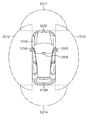
- FIG. 21 is a diagram illustrating an example of an installation position of the imaging unit 12031.
- the imaging unit 12031 includes imaging units 12101, 12102, 12103, 12104, and 12105.
- the imaging units 12101, 12102, 12103, 12104, and 12105 are provided, for example, at positions such as a front nose, a side mirror, a rear bumper, a back door, and an upper portion of a windshield in the vehicle interior of the vehicle 12100.
- the imaging unit 12101 provided in the front nose and the imaging unit 12105 provided in the upper part of the windshield in the vehicle interior mainly acquire an image in front of the vehicle 12100.
- the imaging units 12102 and 12103 provided in the side mirror mainly acquire an image of the side of the vehicle 12100.
- the imaging unit 12104 provided in the rear bumper or the back door mainly acquires an image behind the vehicle 12100.
- the imaging unit 12105 provided on the upper part of the windshield in the passenger compartment is mainly used for detecting a preceding vehicle or a pedestrian, an obstacle, a traffic light, a traffic sign, a lane, or the like.
- FIG. 21 shows an example of the shooting range of the imaging units 12101 to 12104.
- the imaging range 12111 indicates the imaging range of the imaging unit 12101 provided in the front nose
- the imaging ranges 12112 and 12113 indicate the imaging ranges of the imaging units 12102 and 12103 provided in the side mirrors, respectively
- the imaging range 12114 The imaging range of the imaging part 12104 provided in the rear bumper or the back door is shown. For example, by superimposing the image data captured by the imaging units 12101 to 12104, an overhead image when the vehicle 12100 is viewed from above is obtained.
- At least one of the imaging units 12101 to 12104 may have a function of acquiring distance information.
- at least one of the imaging units 12101 to 12104 may be a stereo camera including a plurality of imaging elements, or may be an imaging element having pixels for phase difference detection.
- the microcomputer 12051 based on the distance information obtained from the imaging units 12101 to 12104, the distance to each three-dimensional object in the imaging range 12111 to 12114 and the temporal change in this distance (relative speed with respect to the vehicle 12100).
- a predetermined speed for example, 0 km / h or more
- the microcomputer 12051 can set an inter-vehicle distance to be secured in advance before the preceding vehicle, and can perform automatic brake control (including follow-up stop control), automatic acceleration control (including follow-up start control), and the like.
- automatic brake control including follow-up stop control
- automatic acceleration control including follow-up start control
- cooperative control for the purpose of autonomous driving or the like autonomously traveling without depending on the operation of the driver can be performed.
- the microcomputer 12051 converts the three-dimensional object data related to the three-dimensional object to other three-dimensional objects such as a two-wheeled vehicle, a normal vehicle, a large vehicle, a pedestrian, and a utility pole based on the distance information obtained from the imaging units 12101 to 12104. It can be classified and extracted and used for automatic avoidance of obstacles.
- the microcomputer 12051 identifies obstacles around the vehicle 12100 as obstacles that are visible to the driver of the vehicle 12100 and obstacles that are difficult to see.
- the microcomputer 12051 determines the collision risk indicating the risk of collision with each obstacle, and when the collision risk is equal to or higher than the set value and there is a possibility of collision, the microcomputer 12051 is connected via the audio speaker 12061 or the display unit 12062. By outputting an alarm to the driver and performing forced deceleration or avoidance steering via the drive system control unit 12010, driving assistance for collision avoidance can be performed.
- At least one of the imaging units 12101 to 12104 may be an infrared camera that detects infrared rays.
- the microcomputer 12051 can recognize a pedestrian by determining whether a pedestrian is present in the captured images of the imaging units 12101 to 12104. Such pedestrian recognition is, for example, whether or not the user is a pedestrian by performing a pattern matching process on a sequence of feature points indicating the outline of an object and a procedure for extracting feature points in the captured images of the imaging units 12101 to 12104 as infrared cameras. It is carried out by the procedure for determining.
- the audio image output unit 12052 When the microcomputer 12051 determines that there is a pedestrian in the captured images of the imaging units 12101 to 12104 and recognizes the pedestrian, the audio image output unit 12052 has a rectangular contour line for emphasizing the recognized pedestrian.
- the display unit 12062 is controlled so as to be superimposed and displayed.
- voice image output part 12052 may control the display part 12062 so that the icon etc. which show a pedestrian may be displayed on a desired position.
- the semiconductor device, the manufacturing method thereof, and the electronic device of the present disclosure may have the following configurations.
- An SOI substrate in which a silicon substrate layer, a first insulating layer, and a semiconductor layer are stacked in this order; A first transistor provided on the semiconductor layer; A second transistor provided on the silicon substrate layer and having a higher breakdown voltage than the first transistor; An element isolation film provided between the first transistor and the second transistor; The element isolation film is constituted by a second insulating layer embedded in an opening that penetrates the semiconductor layer and the first insulating layer and reaches the silicon substrate layer, A part of the second insulating layer constitutes a gate insulating film of the second transistor.
- Semiconductor device in which a silicon substrate layer, a first insulating layer, and a semiconductor layer are stacked in this order; A first transistor provided on the semiconductor layer; A second transistor provided on the silicon substrate layer and having a higher breakdown voltage than the first transistor; An element isolation film provided between the first transistor and the second transistor; The element isolation film is constituted by a
- the thickness of the said 2nd insulating layer in the lamination direction is a semiconductor device as described in said (1) thicker than a said 1st insulating layer.
- (8) The method for manufacturing a semiconductor device according to (6) or (7), wherein, before forming the opening in the SOI substrate, a convex portion protruding toward the silicon substrate layer is formed in the opening formation region. .
- (9) Forming the gate electrode of the first transistor and the gate electrode of the second transistor, and then separating the second transistor to form the element isolation film and the gate insulating film of the second transistor; (7) The manufacturing method of the semiconductor device as described in (8).
- a semiconductor device includes: An SOI substrate in which a silicon substrate layer, a first insulating layer, and a semiconductor layer are stacked in this order; A first transistor provided on the semiconductor layer; A second transistor provided on the silicon substrate layer; An element isolation film provided between the first transistor and the second transistor; The element isolation film is constituted by a second insulating layer embedded in an opening that penetrates the semiconductor layer and the first insulating layer and reaches the silicon substrate layer, A part of the second insulating layer constitutes a gate insulating film of the second transistor.
- Electronic equipment is constituted by a second insulating layer embedded in an opening that penetrates the semiconductor layer and the first insulating layer and reaches the silicon substrate layer, A part of the second insulating layer constitutes a gate insulating film of the second transistor.
Landscapes
- Metal-Oxide And Bipolar Metal-Oxide Semiconductor Integrated Circuits (AREA)
- Thin Film Transistor (AREA)
- Solid State Image Pick-Up Elements (AREA)
- Element Separation (AREA)
Abstract
本開示の一実施形態の半導体装置は、シリコン基板層、第1の絶縁層、および半導体層がこの順に積層されたSOI基板と、半導体層上に設けられた第1のトランジスタと、シリコン基板層上に設けられ、第1のトランジスタよりも高耐圧な第2のトランジスタと、第1のトランジスタと第2のトランジスタとの間に設けられた素子分離膜とを備え、素子分離膜は、半導体層および第1の絶縁層を貫通してシリコン基板層内に達する開口に埋設された第2の絶縁層によって構成され、第2の絶縁層の一部は、第2のトランジスタのゲート絶縁膜を構成している。
Description
本開示は、耐圧電圧の異なる複数のトランジスタを備えた半導体装置およびその製造方法並びに電子機器に関する。
近年、医療応用や3次元イメージング等を目的として、さまざまな機能を有するイメージセンサが開発されている。このようなイメージセンサでは、耐圧電圧の異なるトランジスタが搭載されている。例えば、SPAD(Single Photon Avalanche Diode)を用いた測距イメージセンサでは、例えば1V程度以下の電圧で動作する先端トランジスタ(例えばFD(Fully Depleted)-SOIトランジスタ)と、例えば数十V以上の高電圧を受けられるトランジスタ(高耐圧トランジスタ)とが用いられている。前者は、例えばロジック回路に用いられており、後者は、フォトンカウンティングセンサに用いられている。これら耐圧電圧の異なるトランジスタは、通常、異なる基板に形成されている。
これに対して、例えば、特許文献1,2では、耐圧電圧の異なるトランジスタを同一基板上に設けた半導体装置が開示されている。特許文献1に記載の半導体装置では、高耐圧トランジスタは、SOI基板の半導体層上に設けられている。特許文献2に記載の半導体装置では、高耐圧トランジスタは、SOI基板のシリコン基板層上に設けられており、埋め込み酸化膜をゲート絶縁膜として用いている。
ところで、数十V以上の高電圧を受けられる高耐圧トランジスタでは、信頼線の観点から、ゲート絶縁膜は約50nm以上の膜厚が求められる。
耐圧電圧の異なるトランジスタを同一基板上に有し、高い信頼性を備えた半導体装置および半導体装置の製造方法並びに電子機器を提供することが望ましい。
本開示の一実施形態の半導体装置は、シリコン基板層、第1の絶縁層、および半導体層がこの順に積層されたSOI基板と、半導体層上に設けられた第1のトランジスタと、シリコン基板層上に設けられ、第1のトランジスタよりも高耐圧な第2のトランジスタと、第1のトランジスタと第2のトランジスタとの間に設けられた素子分離膜とを備えたものであり、素子分離膜は、半導体層および第1の絶縁層を貫通してシリコン基板層内に達する開口に埋設された第2の絶縁層によって構成され、第2の絶縁層の一部は、第2のトランジスタのゲート絶縁膜を構成している。
本開示の一実施形態の半導体装置の製造方法は、シリコン基板層、第1の絶縁層、および半導体層がこの順に積層されたSOI基板に、半導体層および第1の絶縁層を貫通してシリコン基板層内に達する開口を形成し、開口内に第2の絶縁層を埋設して素子分離膜を形成し、半導体層上に第1のトランジスタを形成し、第2の絶縁層の一部をゲート絶縁膜とし、素子分離膜を間にして、第1のトランジスタより高耐圧な第2のトランジスタをシリコン基板上に形成する。
本開示の一実施形態の電子機器は、上記本開示の一実施形態の半導体装置を備えたものである。
本開示の一実施形態の半導体装置および一実施形態の半導体装置の製造方法並びに一実施形態の電子機器では、第1のトランジスタと、第1のトランジスタよりも高耐圧な第2のトランジスタを有するSOI基板に、SOI基板を構成する半導体層および第1の絶縁層を貫通し、シリコン基板層まで達する開口を設け、この開口を第2の絶縁層によって埋設して素子分離膜を形成した。さらに、第2の絶縁層の一部を、第2のトランジスタのゲート絶縁膜として用いるようにした。これにより、より高耐圧な第2のトランジスタのゲート絶縁膜の厚みを十分に確保することが可能となる。
本開示の一実施形態の半導体装置および一実施形態の半導体装置の製造方法並びに一実施形態の電子機器によれば、SOI基板を構成する第1の絶縁層よりも膜厚の厚い素子分離膜を設け、その素子分離膜を構成する第2の絶縁層の一部を、高耐圧な第2のトランジスタのゲート絶縁膜として用いるようにしたので、SOI基板上に、十分な耐圧性能を有する第2のトランジスタを形成することが可能となる。よって、耐圧電圧の異なるトランジスタを同一基板上に有し、高い信頼性を備えた半導体装置およびこれを備えた電子機器を提供することが可能となる。
なお、ここに記載された効果は必ずしも限定されるものではなく、本開示中に記載されたいずれの効果であってもよい。
以下、本開示における実施の形態について、図面を参照して詳細に説明する。なお、説明は以下の順序で行う。
1.第1の実施の形態(BOX層よりも膜厚の厚い素子分離膜を形成し、その一部を高耐圧トランジスタのゲート絶縁膜とした例)
1-1.半導体装置の構成
1-2.半導体装置の製造方法
1-3.作用・効果
2.第2の実施の形態(レジスト膜のみでゲート電極を形成する例)
3.変形例
3-1.変形例1(素子分離膜部分とゲート絶縁膜部分とで深さの異なる開口を設けた例)
3-2.変形例2(第1の実施の形態の変形例)
3-3.変形例3(第2の実施の形態の変形例)
4.適用例
1.第1の実施の形態(BOX層よりも膜厚の厚い素子分離膜を形成し、その一部を高耐圧トランジスタのゲート絶縁膜とした例)
1-1.半導体装置の構成
1-2.半導体装置の製造方法
1-3.作用・効果
2.第2の実施の形態(レジスト膜のみでゲート電極を形成する例)
3.変形例
3-1.変形例1(素子分離膜部分とゲート絶縁膜部分とで深さの異なる開口を設けた例)
3-2.変形例2(第1の実施の形態の変形例)
3-3.変形例3(第2の実施の形態の変形例)
4.適用例
<1.第1の実施の形態>
図1は、本開示の第1の実施の形態に係る半導体装置(半導体装置1)の断面構成を表したものである。半導体装置1は、同一基板上に、耐圧電圧の異なるトランジスタ(第1のトランジスタおよび第2のトランジスタ)を有するものであり、例えば、SPAD(Single Photon Avalanche Diode)を用いた測距イメージセンサやマイクロコンピュータ等に用いられるものである。半導体装置1は、例えば22nm世代以降の先端トランジスタ(トランジスタ10)と、例えば数十V以上の高電圧を受けられるトランジスタ(トランジスタ20)がSOI基板11上に混載されたものである。SOI基板11は、シリコン基板層12、絶縁層13(第1の絶縁層)および半導体層14がこの順に積層されたものである。本実施の形態では、トランジスタ10は、SOI基板11を構成する半導体層14上に設けられ、トランジスタ20は、SOI基板11を構成するシリコン基板層12上に設けられている。トランジスタ10とトランジスタ20との間には、絶縁層13よりもY軸方向の膜厚(以下、単に厚みという)が厚い素子分離膜21Aが設けられており、素子分離膜21Aを構成する絶縁層21(例えば、図3C参照)の一部がトランジスタ20のゲート絶縁膜21Bとして用いられた構成を有する。
図1は、本開示の第1の実施の形態に係る半導体装置(半導体装置1)の断面構成を表したものである。半導体装置1は、同一基板上に、耐圧電圧の異なるトランジスタ(第1のトランジスタおよび第2のトランジスタ)を有するものであり、例えば、SPAD(Single Photon Avalanche Diode)を用いた測距イメージセンサやマイクロコンピュータ等に用いられるものである。半導体装置1は、例えば22nm世代以降の先端トランジスタ(トランジスタ10)と、例えば数十V以上の高電圧を受けられるトランジスタ(トランジスタ20)がSOI基板11上に混載されたものである。SOI基板11は、シリコン基板層12、絶縁層13(第1の絶縁層)および半導体層14がこの順に積層されたものである。本実施の形態では、トランジスタ10は、SOI基板11を構成する半導体層14上に設けられ、トランジスタ20は、SOI基板11を構成するシリコン基板層12上に設けられている。トランジスタ10とトランジスタ20との間には、絶縁層13よりもY軸方向の膜厚(以下、単に厚みという)が厚い素子分離膜21Aが設けられており、素子分離膜21Aを構成する絶縁層21(例えば、図3C参照)の一部がトランジスタ20のゲート絶縁膜21Bとして用いられた構成を有する。
(1-1.半導体装置の構成)
半導体装置1は、上記のように、SOI基板11上に、素子分離膜21Aを間に、先端トランジスタであるトランジスタ10と、例えば数十V以上の高電圧を受けられるトランジスタ20とが設けられた構成を有する。
半導体装置1は、上記のように、SOI基板11上に、素子分離膜21Aを間に、先端トランジスタであるトランジスタ10と、例えば数十V以上の高電圧を受けられるトランジスタ20とが設けられた構成を有する。
SOI基板11は、バルクシリコンからなるシリコン基板層12上に絶縁層13および半導体層14がこの順に積層されたものである。絶縁層13は、いわゆるBOX層と呼ばれるものであり、例えば20nm以下のシリコン酸化膜(SiO2膜)により構成されている。半導体層14は、例えば6nm以下のシリコン単結晶層により構成されている。
トランジスタ10は、上記のように、22nm世代以降の先端トランジスタであり、例えば完全空乏型シリコン・オン・インシュレータ(FD-SOI)トランジスタである。トランジスタ10は、プレーナ型のトランジスタ構造を有する。トランジスタ10は、半導体層14上にゲート電極15を有する。なお、ゲート電極15と半導体層14との間には、図示していないが、例えば酸化ハフニウム(HfO2)等よりなるゲート絶縁膜が設けられている。ゲート電極15の側面には、例えば窒化シリコン膜よりなるサイドウォール16が設けられている。ゲート電極15に対向する半導体層14には、チャネル領域14Cが設けられている。チャネル領域14Cの両側には、不純物が拡散してなるソース領域14Sおよびドレイン領域14Dが設けられている。一例として、トランジスタ10がNMOSトランジスタである場合には、ソース領域14Sおよびドレイン領域14Dには、例えばイオン注入ドーズ量1E18~19/cm2のリン(P)が拡散される。トランジスタ10が例えばPMOSトランジスタである場合には、ソース領域14Sおよびドレイン領域14Dには、例えば1E18~19/cm2のホウ素(B)が拡散される。
トランジスタ20は、上記のように、例えば十数V~20V以上の高電圧を受けられる、いわゆる高耐圧トランジスタである。トランジスタ20は、シリコン・プレーナ型のトランジスタであり、例えば、ゲート電極22と、シリコン基板層12上に設けられたソース領域23Sおよびドレイン領域23Dと、シリコン基板層12とゲート電極22との間に設けられたゲート絶縁膜21Bとを有している。
ゲート電極22は、シリコン基板層12上に設けられている。但し、ゲート電極22とシリコン基板層12との間には、上記のように、ゲート絶縁膜21Bが設けられている。このゲート絶縁膜21Bは、例えばSiO2膜等よりなり、その厚み(W2)は、SOI基板11のBOX層(絶縁層13)の厚み(W1)よりも厚い。ゲート電極22の側面には、例えば窒化シリコンよりなるサイドウォール24が設けられている。なお、サイドウォール24は、シリコン基板層12上に設けられており、ゲート電極22およびゲート絶縁膜21Bの側面に連続して形成されている。
ソース領域23Sおよびドレイン領域23Dは、ゲート電極22と対向するチャネル領域の両側に、不純物がシリコン基板層12に拡散してなるものである。ソース領域23Sおよびドレイン領域23Dは、例えば、不純物の拡散濃度の高い高濃度拡散領域12Aと、高濃度拡散領域12Aの周囲に設けられ、高濃度拡散領域12Aよりも不純物の拡散濃度の低い低濃度拡散領域12Bとから構成されている。高濃度拡散領域12Aおよび低濃度拡散領域12Bは、例えば以下の構成を有する。例えばトランジスタ20がNMOSトランジスタである場合には、高濃度拡散領域12Aには、例えばイオン注入ドーズ量1E17~18/cm2のリン(P)が拡散されており、低濃度拡散領域12Bには、例えば1E14~15/cm2のリン(P)が拡散されている。また、例えばトランジスタ20が例えばPMOSトランジスタである場合には、高濃度拡散領域12Aには、例えば1E17~18/cm2のホウ素(B)が拡散されており、低濃度拡散領域12Bには、例えば1E14~15/cm2のホウ素(B)が拡散されている。
素子分離膜21Aは、トランジスタ10とトランジスタ20との間に設けられた、例えばSiO2よりなるものである。素子分離膜21Aの厚みは、SOI基板11のBOX層(絶縁層13)よりも厚い。素子分離膜21Aは、詳細は後述するが、例えば、SOI基板11の半導体層14および絶縁層13を貫通すると共に、底面がシリコン基板層12内に存在する開口12Hを埋設する絶縁層21(第2の絶縁層)によって構成されたものである。また、素子分離膜21Aの底面の一部には、シリコン基板層12に突出する凸部21Xが設けられている。この凸部21Xは、先端トランジスタ(トランジスタ10)と高耐圧トランジスタ(トランジスタ20)とが十分に離れて配置されている(例えば10μm以上)場合には必ずしも設ける必要はない。但し、例えば先端トランジスタおよび高耐圧トランジスタをSOI基板上に複数設け、複数の高耐圧トランジスタ(トランジスタ20)が隣接配置された場合には、その間に設けられる素子分離膜21Aの底面に上記凸部21Xを設けることが好ましい。これにより、高耐圧トランジスタ間の絶縁性が向上し、高耐圧トランジスタ間の距離を、例えば1μmに近接して配置できるようになり、チップ面積を縮小化することが可能となる。
絶縁層21は、例えば図5Cに示したように、開口21H1および開口21H2によって分割されており、開口21Hによって分割された絶縁層21が素子分離膜21Aを構成している。また、開口21H1および開口21H2によって分割された絶縁層21がトランジスタ20のゲート絶縁膜21Bを構成している。なお、本実施の形態では、絶縁層21を開口21H1および開口21H2によって3つに分割した例を示したが、これに限らない。例えば開口21H1によって2つに分割し、一方を素子分離膜21Aとして、他方をゲート絶縁膜21Bとして用いるようにしてもよい。但し、上記のように、SOI基板11上に複数のトランジスタを設ける場合には、本実施の形態のように3つに分割することで、残りの絶縁層21の部分を、隣りに配置されたトランジスタとの素子分離膜として用いることができる。
(1-2.半導体装置の製造方法)
本実施の形態の半導体装置1は、例えば、次のようにして製造することができる。
本実施の形態の半導体装置1は、例えば、次のようにして製造することができる。
まず、図2Aに示したように、シリコン基板層12、絶縁層13および半導体層14がこの順に積層されたSOI基板11を用意する。続いて、図2Bに示したように、SOI基板11上(具体的には、半導体層14の表面)に、例えば熱酸化により、例えば1nmの酸化膜31を形成したのち、酸化膜31上に、例えばLPCVD(Low Pressure Chemical Vapor Deposition)法を用いて、例えば30nmの窒化シリコン膜(SiN膜)32を形成する。
次に、図2Cに示したように、SiN膜32上にレジスト膜33を形成したのち、パターニングして開口33Hを形成する。続いて、図2Dに示したように、例えばエッチング法により、凸部21Xとなる、シリコン基板層12内に到達する開口11Hを形成する。
次に、レジスト膜33を除去したのち、図3Aに示したように、SiN膜32上に、開口11Hを含む開口34Hを有するレジスト膜34をパターニングする。続いて、図3Bに示したように、例えばエッチング法により、シリコン基板層12内に到達する開口12Hを形成する。次に、図3Cに示したように、レジスト膜34を除去したのち、例えばHDP-CVD(High-Density Plasma Chemical Vapor Deposition)法を用いて、開口12Hに、例えば酸化シリコン膜(SiO2膜、絶縁層21)を埋設する。続いて、例えばCMP(Chemical Mechanical Polishing)法により、絶縁層21の表面を平坦化する。
次に、図4Aに示したように、例えばウェットエッチング法を用いて絶縁層21をエッチングして任意の厚さに調整する。本実施の形態では、例えば半導体層14と同一面を形成する厚みまでエッチングする。続いて、図4Bに示したように、SiN膜32および酸化膜31を除去したのち、図示していないが、SOI基板11上の全面に、例えばトランジスタ10のゲート絶縁膜となる、例えばハフニウム酸化膜(HfO2膜)を、例えば2nmの厚みで形成する。次に、図4Cに示したように、SOI基板11の半導体層14および絶縁層21上(実際には、HfO2膜上)に、例えばCVD法を用いてポリシリコン(Si)膜15Aを成膜する。なお、ポリSi膜15Aを形成する際には、HfO2膜がトランジスタ10の形成領域のみにパターニングされていてもよいが、HfO2膜の有無は、トランジスタ20の特性に特に影響がないため、SOI基板11の全面に形成された状態でもよい。
続いて、図5Aに示したように、ポリSi膜15A上に、例えばCVD法を用いてSiN膜35を成膜したのち、SiN膜35上にレジスト膜36をパターニングする。次に、図5Bに示したように、例えばエッチング法によりSiN膜35およびポリSi膜15Aをエッチングする。これにより、トランジスタ10およびトランジスタ20のゲート電極15,22がHfO2膜上に一括で形成される。続いて、レジスト膜36を除去したのち、SOI基板11上に、トランジスタ20のゲート電極22を含む開口を有するレジスト膜37をパターニングする。次に、図5Cに示したように、例えばエッチング法を用いて、レジスト膜37の開口内の絶縁層21をエッチングする。このときゲート電極22上のSiN膜35がエッチングマスクとなり、絶縁層21には、開口21H1および開口21H2が形成される。これにより、絶縁層21は、3つに分割され、ゲート電極22の下方の絶縁層21はトランジスタ20のゲート絶縁膜21Bとなり、トランジスタ10側に分割された絶縁層21は、トランジスタ10とトランジスタ20とを電気的に分離する素子分離膜21Aとなる。続いて、レジスト膜37を除去する。
次に、トランジスタ10のゲート電極15の両側の半導体層14に、例えばイオン注入法を用いて、ソース領域14Sおよびドレイン領域14Dを形成したのち、図6Aに示したように、開口21H1,21H2内のシリコン基板層12に、例えばイオン注入法を用いて低濃度拡散領域12Bを形成する。続いて、例えばCVD法を用いて例えばSiN膜を成膜したのち、エッチバックを行いトランジスタ10のゲート電極15の側面およびトランジスタ20のゲート電極22およびゲート絶縁膜21Bの連続する側面にサイドウォール16,24をそれぞれ形成する。このとき、開口21H1,21H2を構成する素子分離膜21Aの側面およびゲート絶縁膜21Bを挟んだ反対側の絶縁層21の側面にも、サイドウォール24と同様の形状を有するSiN膜が形成される。次に、開口21H1,21H2内のシリコン基板層12に、例えばイオン注入法を用いて高濃度拡散領域12Aを形成する。このとき、サイドウォール24および素子分離膜21Aの側面およびゲート絶縁膜21Bを挟んだ反対側の絶縁層21の側面に形成されたSiN膜がマスクとなって、高濃度拡散領域12Aは、先に形成した低濃度拡散領域12Bの内部に形成される。これにより、図1に示した半導体装置1が完成する。
なお、本実施の形態の半導体装置1は、上記のように、例えば測距イメージセンサ等に用いられる。例えば図17に示した撮像装置4では、図1に示した半導体装置1上に光電変換部を有する画素部50が配設される。画素部50には、複数の単位画素Pがマトリクス上に配置されており、例えば、単位画素Pにそれぞれ、トランジスタ10およびトランジスタ20が配設される。その場合には、図6Bに示したように、半導体装置1上に、例えばシリコン酸化膜やリンやボロンを含んだシリコン酸化膜等からなる層間絶縁層41を例えばCVD法を用いて形成したのち、層間絶縁層41内に、コンタクトプラグP1,P2,P3,P4,P5,P6を形成する。コンタクトプラグP1,P2,P3,P4,P5,P6の一端は、図6Bに示したように、それぞれトランジスタ10のゲート電極15、ソース領域14Sおよびドレイン領域14D、トランジスタ20のゲート電極22、ソース領域23Sおよびドレイン領域23Dと電気的に接続されている。他端は、単位画素Pの所定の部位に接続されている。
(1-3.作用・効果)
同一基板上に耐圧電圧の異なるトランジスタを設ける場合、一般的には、マルチオキサイドプロセスを用いて低電圧動作トランジスタおよび高電圧動作トランジスタのゲート絶縁膜を作り分けている。具体的には、まず、図7Aに示したようにシリコン基板101を厚膜酸化してSiO2膜102を形成したのち、図7Bに示したように、所定の領域(例えば低電圧動作トランジスタを形成する領域)のSiO2膜102を除去する。こののち、図7Cに示したようにシリコン基板101を薄膜酸化することで、シリコン基板101上に異なる厚みのSiO2膜102が形成される。
同一基板上に耐圧電圧の異なるトランジスタを設ける場合、一般的には、マルチオキサイドプロセスを用いて低電圧動作トランジスタおよび高電圧動作トランジスタのゲート絶縁膜を作り分けている。具体的には、まず、図7Aに示したようにシリコン基板101を厚膜酸化してSiO2膜102を形成したのち、図7Bに示したように、所定の領域(例えば低電圧動作トランジスタを形成する領域)のSiO2膜102を除去する。こののち、図7Cに示したようにシリコン基板101を薄膜酸化することで、シリコン基板101上に異なる厚みのSiO2膜102が形成される。
ところで、例えばSPADを用いた測距イメージセンサでは、前述したように、例えば22nm世代以降の先端トランジスタ(例えば、FD-SOIトランジスタ)と、数十V以上の高電圧を受けられるトランジスタ(高耐圧トランジスタ)とが用いられている。FD-SOIトランジスタは、シリコン基板上に絶縁層(BOX層)を介して薄いSi層が設けられたSOI基板に形成されている。高耐圧トランジスタを、上記方法を用いてこのSOI基板上に混載しようとした場合、厚膜酸化時にSi層が全て酸化されてしまう。
また、前述したように、SOI基板のBOX層を高耐圧トランジスタのゲート絶縁膜として用いる方法が考えられている。しかしながら、数十V以上の高電圧を受けられる高耐圧トランジスタでは、信頼性の観点から、ゲート絶縁膜は例えば50nm以上の厚みが求められており、通常20nm程度のBOX層では、高耐圧トランジスタのゲート絶縁膜としては耐圧不足となる。そこで、BOX層の厚みを厚く(例えば50nm程度)することも考えられるが、その場合には、FD-SOIトランジスタで行われているバックバイアス制御ができなくなってしまう。
この他、LOCOS(local oxidation of silicon)法を用いてBOX層を部分的に厚膜化する方法が考えられる。しかしながら、LOCOS法を用いてBOX層を厚膜化した場合、その近傍は局所的熱酸化による堆積膨張が生じ、SOI基板の表面には段差が形成される。ところで、微細化が進んだ半導体装置では、リソグラフィ工程における焦点深度(Depth Of Focus;DOF)は小さくなる。このため、リソグラフィ工程により形成されたレジスト膜の線幅にばらつきが生じやすくなり、このばらつきを抑制するためには、レジスト膜を形成する下地の段差は小さくすることが望ましい。これに対して、LOCOS法の局所的熱酸化によって生じるSOI基板の表面の段差は、レジスト膜の線幅のばらつきの一因となる。
本実施の形態では、SOI基板11に、素子分離膜21Aとして、SOI基板11を構成する半導体層14および絶縁層13を貫通し、シリコン基板層12まで達する開口12Hを形成し、その開口12Hに絶縁層21を埋設し、その一部を高耐圧トランジスタ(トランジスタ20)のゲート絶縁膜21Bとして用いるようにした。絶縁層21の厚みは、開口12Hの深さを調整することで任意に設定することができる。これにより、先端トランジスタであるトランジスタ10の動作や、製造工程に影響を与えることなく、高耐圧なトランジスタ20のゲート絶縁膜21Bの厚みを十分に確保することが可能となる。
以上、本実施の形態の半導体装置1では、FD-SOIトランジスタであるトランジスタ10と、高耐圧トランジスタであるトランジスタ20との間に、SOI基板11を構成する絶縁層13よりも膜厚の大きな素子分離膜21Aを設け、その素子分離膜21Aを構成する絶縁層21の一部を、トランジスタ20のゲート絶縁膜として用いるようにした。具体的には、SOI基板11に、半導体層14および絶縁層13を貫通し、シリコン基板層12内まで達する開口12Hを設け、その開口12Hを絶縁層21で埋設し、この絶縁層21を分割して、一方を素子分離膜21Aとして、他方をトランジスタ20のゲート絶縁膜として用いるようにした。これにより、高耐圧トランジスタであるトランジスタ20のゲート絶縁膜として、十分な耐圧性能を有するゲート絶縁膜21Bが形成される。よって、耐圧電圧の異なるトランジスタを同一基板上に有し、高い信頼性を備えた半導体装置1を提供することが可能となる。
また、素子分離膜21Aの底面に、シリコン基板層12に突出する凸部21Xを設けるようにしたので、トランジスタ10とトランジスタ20との間の電気的な絶縁性が向上し、トランジスタ10とトランジスタ20との距離を削減することが可能となる。また、複数のトランジスタ20が隣接配置される場合には、その間に凸部21Xを設けることにより、トランジスタ20間の距離を削減することが可能となる。よって、チップ面積を縮小化することが可能となる。
以下、本開示の第2の実施の形態および変形例1~3について説明する。なお、上記第1の実施の形態と同一の構成要素については同一の符号を付し説明を省略する。
<2.第2の実施の形態>
図8A~8Bは、本開示の第2の実施の形態に係る半導体装置1の製造方法の他の例を模式的に表したものである。
図8A~8Bは、本開示の第2の実施の形態に係る半導体装置1の製造方法の他の例を模式的に表したものである。
本実施の形態の製造方法では、上記第1の実施の形態において説明した方法を用いて、図8Aに示したように、SOI基板11上にポリSi膜15Aを形成したのち、図8Bに示したように、SiN膜35を形成することなく、Si膜15A上にレジスト膜36をパターニングする。続いて、図8Cに示したように、レジスト膜36をマスクとして、ポリSi膜15Aをエッチングし、トランジスタ10のゲート電極15およびトランジスタ20のゲート電極22を形成する。こののち、レジスト膜36を除去する。次に、図8Dに示したように、SOI基板11の半導体層14および絶縁層21上に、レジスト膜38をパターニングしたのち、第1の実施の形態と同様の方法を用いて絶縁層21をエッチングする。これにより、絶縁層21内に開口21H1および開口21H2が形成され、絶縁層21が3つに分割される。以降、第1の実施の形態と同様の方法を用いることにより、図1に示した半導体装置1が完成する。
本実施の形態では、開口21H1および開口21H2を形成する絶縁層21のエッチングの際のマスクとなるSiN膜35を形成することなく、半導体装置1を形成するようにした。これにより、上記第1の実施の形態における半導体装置1の製造方法と比較して、製造工程数を削減することが可能となる。
<3.変形例>
(3-1.変形例1)
図9は、本開示の変形例1に係る半導体装置(半導体装置2)の断面構成を表したものである。本変形例の半導体装置2は、複数(ここでは、3種)の深さを有する開口12Hを形成し、底面に段差を有する絶縁層21を設けたものである。具体的には、第1の実施の形態において説明した凸部21Xを挟んで、素子分離膜21Aがゲート絶縁膜21Bよりも厚くなるようにした。このように、素子分離膜21Aおよびゲート絶縁膜21Bの厚みは、適宜調整することができる。
(3-1.変形例1)
図9は、本開示の変形例1に係る半導体装置(半導体装置2)の断面構成を表したものである。本変形例の半導体装置2は、複数(ここでは、3種)の深さを有する開口12Hを形成し、底面に段差を有する絶縁層21を設けたものである。具体的には、第1の実施の形態において説明した凸部21Xを挟んで、素子分離膜21Aがゲート絶縁膜21Bよりも厚くなるようにした。このように、素子分離膜21Aおよびゲート絶縁膜21Bの厚みは、適宜調整することができる。
(3-2.変形例2)
図10A~図14Cは、上記第1の実施の形態の変形例としての半導体装置(半導体装置3、図14C参照)の製造方法を表したものである。本変形例の半導体装置3は、トランジスタ10およびトランジスタ20が、SOI基板11上に複数(本変形例では、それぞれ2個ずつ、トランジスタ10X,10Yおよびトランジスタ20X,20Y)設けられたものである。このような半導体装置3は、例えば、次のようにして製造することができる。
図10A~図14Cは、上記第1の実施の形態の変形例としての半導体装置(半導体装置3、図14C参照)の製造方法を表したものである。本変形例の半導体装置3は、トランジスタ10およびトランジスタ20が、SOI基板11上に複数(本変形例では、それぞれ2個ずつ、トランジスタ10X,10Yおよびトランジスタ20X,20Y)設けられたものである。このような半導体装置3は、例えば、次のようにして製造することができる。
まず、例えば、第1の実施の形態と同様の方法を用いて、SOI基板11上に酸化膜31およびSiN膜32を形成する。続いて、図10Aに示したように、SiN膜32上にレジスト膜33を形成したのち、パターニングして、例えば4つの開口33H1~33H4を形成する。続いて、図10Bに示したように、例えばエッチング法により、シリコン基板層12内に到達する開口11H1~11H4を形成する。次に、レジスト膜33を除去したのち、図10Cに示したように、SiN膜32上に、トランジスタ20X,20Yの形成領域20Rに開口を有するレジスト膜34をパターニングする。
次に、図11Aに示したように、例えばエッチング法により、シリコン基板層12内に到達する開口12Hを形成する。続いて、レジスト膜34を除去したのち、図11Bに示したように、例えばHDP-CVD法を用いて開口11H1,11H2内および開口11H3,11H4を含む開口12H内並びにSiN膜32上に、例えばSiO2膜(絶縁層21)を成膜する。次に、図11Cに示したように、例えばCMP法により、絶縁層21の表面を平坦化する。これにより、最終的に隣接配置されるトランジスタ10X,10Yおよびトランジスタ20X,20Yをそれぞれ電気的に絶縁する凸部21X1,21X2,21X3,21X4が形成される。
続いて、図12Aに示したように、例えばウェットエッチング法を用いて絶縁層21を任意の厚さに調整したのち、SiN膜32および酸化膜31を除去する。次に、第1の実施の形態と同様に、図示していないが、SOI基板11上の全面に、例えばトランジスタ10のゲート絶縁膜となる、例えばHfO2膜を、例えば2nmの厚みで形成したのち、図12Bに示したように、例えばCVD法を用いてポリシリコン(Si)膜15AおよびSiN膜35をこの順に成膜する。続いて、図12Cに示したように、SiN膜35上にレジスト膜36をパターニングする。
次に、図13Aに示したように、例えばエッチング法により、レジスト膜36をマスクとしてSiN膜35およびポリSi膜15Aをエッチングする。これにより、トランジスタ10X,10Yおよびトランジスタ20X,20Yのゲート電極15X,15Y,22X,22Yが一括で形成される。続いて、レジスト膜36を除去したのち、図13Bに示したように、SOI基板11の半導体層14および絶縁層21上にレジスト膜37をパターニングする。次に、例えばエッチング法を用いて、絶縁層21をエッチングする。このとき、レジスト膜37と共に、ゲート電極22上のSiN膜35がエッチングマスクとなり、開口21H1,21H2,21H3,21H4が形成される。これにより、開口12H内の絶縁層21は、5つに分割され、それぞれ、トランジスタ20X,20Yのゲート絶縁膜21B1,21B2、トランジスタ10とトランジスタ20とを電気的に分離する素子分離膜21A、トランジスタ20Xとトランジスタ20Yとの間を電気的に絶縁する素子分離膜(絶縁膜21B3)および例えば、図示していないがトランジスタ20Yのトランジスタ20Xとは反対側に別のトランジスタが形成された際の素子分離膜(絶縁膜21B4)となる。続いて、図13Cに示したように、レジスト膜37および各ゲート電極15X,15Y,22X,22Y上に設けられたSiN膜35を除去する。
次に、トランジスタ10X,10Yの両側の半導体層14に、例えばイオン注入法を用いて、ソース領域14S1,14S2およびドレイン領域14D1,14D2を形成する。こののち、図14Aに示したように、トランジスタ10X,10Yを含む半導体層14上および素子分離膜21A上にレジスト膜39を形成する。続いて、開口21H1,21H2および開口21H3,21H4内のシリコン基板層12に、例えばイオン注入法を用いて、それぞれ低濃度拡散領域12B1,12B2を形成する。次に、レジスト膜39を除去したのち、図14Bに示したように、例えばCVD法を用いて例えばSiN膜を成膜し、エッチバックを行いてトランジスタ10X,10Yのゲート電極15X,15Yの側面およびトランジスタ20X,20Yのゲート電極22Xとゲート絶縁膜21B1およびゲート電極22Yとゲート絶縁膜21B2の連続する側面にサイドウォール16,24をそれぞれ形成する。このとき、素子分離膜21Aおよび各トランジスタ間の素子分離膜となる絶縁膜21B3,21B4の側面にもサイドウォールと同様の形状を有するSiN膜が形成される。続いて、再度、トランジスタ10X,10Yを含む半導体層14上および素子分離膜21A上にレジスト膜40を形成する。次に、図14Cに示したように、開口21H1,21H2,21H3,21H4内のシリコン基板層12に例えばイオン注入法を用いて高濃度拡散領域12A1,12A2を形成する。このとき、サイドウォール24と、素子分離膜21Aおよび絶縁膜21B3,21B4の側面に形成されるSiN膜とがマスクとなって、高濃度拡散領域12A1,12A2は、先に形成した低濃度拡散領域12B1,12B2の内部に形成される。最後に、レジスト膜40を除去することにより、隣り合うトランジスタ10Xとトランジスタ10Yとの間、トランジスタ10Yとトランジスタ20Xとの間、トランジスタ20Xとトランジスタ20Yとの間にそれぞれ凸部21X1,21X2,21X3,21X4を有する半導体装置3が完成する。
なお、ここでは、トランジスタ10Yとトランジスタ20Xとの間に2つの凸部21X2,21X3を設けた例を示したが、先端トランジスタ(トランジスタ10Y)と高耐圧トランジスタ(トランジスタ20X)との間には、少なくとも凸部の先端がより深い位置にある凸部21X3を形成すれば、凸部21X2は省略してもかまわない。
(3-3.変形例3)
図15A~図16Bは、上記第2の実施の形態の変形例としての半導体装置3の製造方法を表したものである。本変形例では、半導体装置3は、例えば次のようにして製造することができる。
図15A~図16Bは、上記第2の実施の形態の変形例としての半導体装置3の製造方法を表したものである。本変形例では、半導体装置3は、例えば次のようにして製造することができる。
まず、変形例1と同様の方法を用いて、凸部21X1,21X2,21X3,21X4を形成したのち、図15Aに示したように、SOI基板11の半導体層14および絶縁層21上(実際には、HfO2膜上)に、例えばCVD法を用いてポリシリコン(Si)膜15Aを成膜する。続いて、図15Bに示したように、Si膜15A上にレジスト膜36をパターニングする。続いて、図15Cに示したように、レジスト膜36をマスクとしてポリSi膜15Aをエッチングし、それぞれ、トランジスタ10X,10Yのゲート電極15X,15Yおよびトランジスタ20X,20Yのゲート電極22X,22Yを形成する。
次に、レジスト膜36を除去したのち、SOI基板11の半導体層14および絶縁層21上に、レジスト膜38をパターニングしたのち、第1の実施の形態と同様の方法を用いて絶縁層21をエッチングし、図16Bに示したように、開口21H1,21H2,21H3,21H4を形成する。以降、変形例1と同様の方法を用いることにより、図14Cに示した半導体装置3が完成する。
<4.適用例>
(適用例1)
図17は、上記第1の実施の形態(または変形例)に示した半導体装置(半導体装置1,2)を備えた撮像素子を各単位画素Pに用いた撮像装置(撮像装置4)の全体構成を表したものである。この撮像装置4は、CMOSイメージセンサであり、例えば、SOI基板11上に、撮像エリアとしての画素部50を有すると共に、この画素部50の周辺領域に、例えば、行走査部131、水平選択部133、列走査部134およびシステム制御部132からなる周辺回路部130を有している。
(適用例1)
図17は、上記第1の実施の形態(または変形例)に示した半導体装置(半導体装置1,2)を備えた撮像素子を各単位画素Pに用いた撮像装置(撮像装置4)の全体構成を表したものである。この撮像装置4は、CMOSイメージセンサであり、例えば、SOI基板11上に、撮像エリアとしての画素部50を有すると共に、この画素部50の周辺領域に、例えば、行走査部131、水平選択部133、列走査部134およびシステム制御部132からなる周辺回路部130を有している。
画素部50は、例えば、行列状に2次元配置された複数の単位画素P(撮像素子に相当)を有している。この単位画素Pには、例えば、画素行ごとに画素駆動線Lread(具体的には行選択線およびリセット制御線)が配線され、画素列ごとに垂直信号線Lsigが配線されている。画素駆動線Lreadは、画素からの信号読み出しのための駆動信号を伝送するものである。画素駆動線Lreadの一端は、行走査部131の各行に対応した出力端に接続されている。
行走査部131は、シフトレジスタやアドレスデコーダ等によって構成され、画素部50の各単位画素Pを、例えば、行単位で駆動する画素駆動部である。行走査部131によって選択走査された画素行の各単位画素Pから出力される信号は、垂直信号線Lsigの各々を通して水平選択部133に供給される。水平選択部133は、垂直信号線Lsigごとに設けられたアンプや水平選択スイッチ等によって構成されている。
列走査部134は、シフトレジスタやアドレスデコーダ等によって構成され、水平選択部133の各水平選択スイッチを走査しつつ順番に駆動するものである。この列走査部134による選択走査により、垂直信号線Lsigの各々を通して伝送される各画素の信号が順番に水平信号線135に出力され、当該水平信号線135を通してSOI基板11の外部へ伝送される。
行走査部131、水平選択部133、列走査部134および水平信号線135からなる回路部分は、SOI基板11上に直に形成されていてもよいし、あるいは外部制御ICに配設されたものであってもよい。また、それらの回路部分は、ケーブル等により接続された他の基板に形成されていてもよい。
システム制御部132は、SOI基板11の外部から与えられるクロックや、動作モードを指令するデータ等を受け取り、また、撮像装置4の内部情報等のデータを出力するものである。システム制御部132はさらに、各種のタイミング信号を生成するタイミングジェネレータを有し、当該タイミングジェネレータで生成された各種のタイミング信号を基に行走査部131、水平選択部133および列走査部134等の周辺回路の駆動制御を行う。
(適用例2)
上記撮像装置4は、例えば、デジタルスチルカメラやビデオカメラ等のカメラシステムや、撮像機能を有する携帯電話等、撮像機能を備えたあらゆるタイプの電子機器に適用することができる。図18に、その一例として、電子機器5(カメラ)の概略構成を示す。この電子機器5は、例えば、静止画または動画を撮影可能なビデオカメラであり、撮像装置4と、光学系(光学レンズ)310と、シャッタ装置311と、撮像装置4およびシャッタ装置311を駆動する駆動部313と、信号処理部312とを有する。
上記撮像装置4は、例えば、デジタルスチルカメラやビデオカメラ等のカメラシステムや、撮像機能を有する携帯電話等、撮像機能を備えたあらゆるタイプの電子機器に適用することができる。図18に、その一例として、電子機器5(カメラ)の概略構成を示す。この電子機器5は、例えば、静止画または動画を撮影可能なビデオカメラであり、撮像装置4と、光学系(光学レンズ)310と、シャッタ装置311と、撮像装置4およびシャッタ装置311を駆動する駆動部313と、信号処理部312とを有する。
光学系310は、被写体からの像光(入射光)を撮像装置4の画素部50へ導くものである。この光学系310は、複数の光学レンズから構成されていてもよい。シャッタ装置311は、撮像装置4への光照射期間および遮光期間を制御するものである。駆動部313は、撮像装置4の転送動作およびシャッタ装置311のシャッタ動作を制御するものである。信号処理部312は、撮像装置4から出力された信号に対し、各種の信号処理を行うものである。信号処理後の映像信号Doutは、メモリ等の記憶媒体に記憶されるか、あるいは、モニタ等に出力される。
更に、上記撮像装置4は、下記電子機器(カプセル型内視鏡10100および車両等の移動体)にも適用することが可能である。
(適用例3)
<体内情報取得システムへの応用例>
図19は、本開示に係る技術(本技術)が適用され得る、カプセル型内視鏡を用いた患者の体内情報取得システムの概略的な構成の一例を示すブロック図である。
<体内情報取得システムへの応用例>
図19は、本開示に係る技術(本技術)が適用され得る、カプセル型内視鏡を用いた患者の体内情報取得システムの概略的な構成の一例を示すブロック図である。
体内情報取得システム10001は、カプセル型内視鏡10100と、外部制御装置10200とから構成される。
カプセル型内視鏡10100は、検査時に、患者によって飲み込まれる。カプセル型内視鏡10100は、撮像機能および無線通信機能を有し、患者から自然排出されるまでの間、胃や腸等の臓器の内部を蠕動運動等によって移動しつつ、当該臓器の内部の画像(以下、体内画像ともいう)を所定の間隔で順次撮像し、その体内画像についての情報を体外の外部制御装置10200に順次無線送信する。
外部制御装置10200は、体内情報取得システム10001の動作を統括的に制御する。また、外部制御装置10200は、カプセル型内視鏡10100から送信されてくる体内画像についての情報を受信し、受信した体内画像についての情報に基づいて、表示装置(図示せず)に当該体内画像を表示するための画像データを生成する。
体内情報取得システム10001では、このようにして、カプセル型内視鏡10100が飲み込まれてから排出されるまでの間、患者の体内の様子を撮像した体内画像を随時得ることができる。
カプセル型内視鏡10100と外部制御装置10200の構成および機能についてより詳細に説明する。
カプセル型内視鏡10100は、カプセル型の筐体10101を有し、その筐体10101内には、光源部10111、撮像部10112、画像処理部10113、無線通信部10114、給電部10115、電源部10116、および制御部10117が収納されている。
光源部10111は、例えばLED(light emitting diode)等の光源から構成され、撮像部10112の撮像視野に対して光を照射する。
撮像部10112は、撮像素子、および当該撮像素子の前段に設けられる複数のレンズからなる光学系から構成される。観察対象である体組織に照射された光の反射光(以下、観察光という)は、当該光学系によって集光され、当該撮像素子に入射する。撮像部10112では、撮像素子において、そこに入射した観察光が光電変換され、その観察光に対応する画像信号が生成される。撮像部10112によって生成された画像信号は、画像処理部10113に提供される。
画像処理部10113は、CPU(Central Processing Unit)やGPU(Graphics Processing Unit)等のプロセッサによって構成され、撮像部10112によって生成された画像信号に対して各種の信号処理を行う。画像処理部10113は、信号処理を施した画像信号を、RAWデータとして無線通信部10114に提供する。
無線通信部10114は、画像処理部10113によって信号処理が施された画像信号に対して変調処理等の所定の処理を行い、その画像信号を、アンテナ10114Aを介して外部制御装置10200に送信する。また、無線通信部10114は、外部制御装置10200から、カプセル型内視鏡10100の駆動制御に関する制御信号を、アンテナ10114Aを介して受信する。無線通信部10114は、外部制御装置10200から受信した制御信号を制御部10117に提供する。
給電部10115は、受電用のアンテナコイル、当該アンテナコイルに発生した電流から電力を再生する電力再生回路、および昇圧回路等から構成される。給電部10115では、いわゆる非接触充電の原理を用いて電力が生成される。
電源部10116は、二次電池によって構成され、給電部10115によって生成された電力を蓄電する。図19では、図面が煩雑になることを避けるために、電源部10116からの電力の供給先を示す矢印等の図示を省略しているが、電源部10116に蓄電された電力は、光源部10111、撮像部10112、画像処理部10113、無線通信部10114、および制御部10117に供給され、これらの駆動に用いられ得る。
制御部10117は、CPU等のプロセッサによって構成され、光源部10111、撮像部10112、画像処理部10113、無線通信部10114、および、給電部10115の駆動を、外部制御装置10200から送信される制御信号に従って適宜制御する。
外部制御装置10200は、CPU,GPU等のプロセッサ、又はプロセッサとメモリ等の記憶素子が混載されたマイクロコンピュータ若しくは制御基板等で構成される。外部制御装置10200は、カプセル型内視鏡10100の制御部10117に対して制御信号を、アンテナ10200Aを介して送信することにより、カプセル型内視鏡10100の動作を制御する。カプセル型内視鏡10100では、例えば、外部制御装置10200からの制御信号により、光源部10111における観察対象に対する光の照射条件が変更され得る。また、外部制御装置10200からの制御信号により、撮像条件(例えば、撮像部10112におけるフレームレート、露出値等)が変更され得る。また、外部制御装置10200からの制御信号により、画像処理部10113における処理の内容や、無線通信部10114が画像信号を送信する条件(例えば、送信間隔、送信画像数等)が変更されてもよい。
また、外部制御装置10200は、カプセル型内視鏡10100から送信される画像信号に対して、各種の画像処理を施し、撮像された体内画像を表示装置に表示するための画像データを生成する。当該画像処理としては、例えば現像処理(デモザイク処理)、高画質化処理(帯域強調処理、超解像処理、NR(Noise reduction)処理および/又は手ブレ補正処理等)、並びに/又は拡大処理(電子ズーム処理)等、各種の信号処理を行うことができる。外部制御装置10200は、表示装置の駆動を制御して、生成した画像データに基づいて撮像された体内画像を表示させる。あるいは、外部制御装置10200は、生成した画像データを記録装置(図示せず)に記録させたり、印刷装置(図示せず)に印刷出力させてもよい。
以上、本開示に係る技術が適用され得る体内情報取得システムの一例について説明した。本開示に係る技術は、以上説明した構成のうち、例えば、撮像部10112に適用され得る。これにより、精細な術部画像を得ることができるため、検査の精度が向上する。
(適用例4)
<移動体への応用例>
本開示に係る技術(本技術)は、様々な製品へ応用することができる。例えば、本開示に係る技術は、自動車、電気自動車、ハイブリッド電気自動車、自動二輪車、自転車、パーソナルモビリティ、飛行機、ドローン、船舶、ロボット等のいずれかの種類の移動体に搭載される装置として実現されてもよい。
<移動体への応用例>
本開示に係る技術(本技術)は、様々な製品へ応用することができる。例えば、本開示に係る技術は、自動車、電気自動車、ハイブリッド電気自動車、自動二輪車、自転車、パーソナルモビリティ、飛行機、ドローン、船舶、ロボット等のいずれかの種類の移動体に搭載される装置として実現されてもよい。
図20は、本開示に係る技術が適用され得る移動体制御システムの一例である車両制御システムの概略的な構成例を示すブロック図である。
車両制御システム12000は、通信ネットワーク12001を介して接続された複数の電子制御ユニットを備える。図20に示した例では、車両制御システム12000は、駆動系制御ユニット12010、ボディ系制御ユニット12020、車外情報検出ユニット12030、車内情報検出ユニット12040、および統合制御ユニット12050を備える。また、統合制御ユニット12050の機能構成として、マイクロコンピュータ12051、音声画像出力部12052、および車載ネットワークI/F(interface)12053が図示されている。
駆動系制御ユニット12010は、各種プログラムにしたがって車両の駆動系に関連する装置の動作を制御する。例えば、駆動系制御ユニット12010は、内燃機関又は駆動用モータ等の車両の駆動力を発生させるための駆動力発生装置、駆動力を車輪に伝達するための駆動力伝達機構、車両の舵角を調節するステアリング機構、および、車両の制動力を発生させる制動装置等の制御装置として機能する。
ボディ系制御ユニット12020は、各種プログラムにしたがって車体に装備された各種装置の動作を制御する。例えば、ボディ系制御ユニット12020は、キーレスエントリシステム、スマートキーシステム、パワーウィンドウ装置、あるいは、ヘッドランプ、バックランプ、ブレーキランプ、ウィンカー又はフォグランプ等の各種ランプの制御装置として機能する。この場合、ボディ系制御ユニット12020には、鍵を代替する携帯機から発信される電波又は各種スイッチの信号が入力され得る。ボディ系制御ユニット12020は、これらの電波又は信号の入力を受け付け、車両のドアロック装置、パワーウィンドウ装置、ランプ等を制御する。
車外情報検出ユニット12030は、車両制御システム12000を搭載した車両の外部の情報を検出する。例えば、車外情報検出ユニット12030には、撮像部12031が接続される。車外情報検出ユニット12030は、撮像部12031に車外の画像を撮像させるとともに、撮像された画像を受信する。車外情報検出ユニット12030は、受信した画像に基づいて、人、車、障害物、標識又は路面上の文字等の物体検出処理又は距離検出処理を行ってもよい。
撮像部12031は、光を受光し、その光の受光量に応じた電気信号を出力する光センサである。撮像部12031は、電気信号を画像として出力することもできるし、測距の情報として出力することもできる。また、撮像部12031が受光する光は、可視光であっても良いし、赤外線等の非可視光であっても良い。
車内情報検出ユニット12040は、車内の情報を検出する。車内情報検出ユニット12040には、例えば、運転者の状態を検出する運転者状態検出部12041が接続される。運転者状態検出部12041は、例えば運転者を撮像するカメラを含み、車内情報検出ユニット12040は、運転者状態検出部12041から入力される検出情報に基づいて、運転者の疲労度合い又は集中度合いを算出してもよいし、運転者が居眠りをしていないかを判別してもよい。
マイクロコンピュータ12051は、車外情報検出ユニット12030又は車内情報検出ユニット12040で取得される車内外の情報に基づいて、駆動力発生装置、ステアリング機構又は制動装置の制御目標値を演算し、駆動系制御ユニット12010に対して制御指令を出力することができる。例えば、マイクロコンピュータ12051は、車両の衝突回避あるいは衝撃緩和、車間距離に基づく追従走行、車速維持走行、車両の衝突警告、又は車両のレーン逸脱警告等を含むADAS(Advanced Driver Assistance System)の機能実現を目的とした協調制御を行うことができる。
また、マイクロコンピュータ12051は、車外情報検出ユニット12030又は車内情報検出ユニット12040で取得される車両の周囲の情報に基づいて駆動力発生装置、ステアリング機構又は制動装置等を制御することにより、運転者の操作に拠らずに自律的に走行する自動運転等を目的とした協調制御を行うことができる。
また、マイクロコンピュータ12051は、車外情報検出ユニット12030で取得される車外の情報に基づいて、ボディ系制御ユニット12020に対して制御指令を出力することができる。例えば、マイクロコンピュータ12051は、車外情報検出ユニット12030で検知した先行車又は対向車の位置に応じてヘッドランプを制御し、ハイビームをロービームに切り替える等の防眩を図ることを目的とした協調制御を行うことができる。
音声画像出力部12052は、車両の搭乗者又は車外に対して、視覚的又は聴覚的に情報を通知することが可能な出力装置へ音声および画像のうちの少なくとも一方の出力信号を送信する。図20の例では、出力装置として、オーディオスピーカ12061、表示部12062およびインストルメントパネル12063が例示されている。表示部12062は、例えば、オンボードディスプレイおよびヘッドアップディスプレイの少なくとも一つを含んでいてもよい。
図21は、撮像部12031の設置位置の例を示す図である。
図21では、撮像部12031として、撮像部12101,12102,12103,12104,12105を有する。
撮像部12101,12102,12103,12104,12105は、例えば、車両12100のフロントノーズ、サイドミラー、リアバンパ、バックドアおよび車室内のフロントガラスの上部等の位置に設けられる。フロントノーズに備えられる撮像部12101および車室内のフロントガラスの上部に備えられる撮像部12105は、主として車両12100の前方の画像を取得する。サイドミラーに備えられる撮像部12102,12103は、主として車両12100の側方の画像を取得する。リアバンパ又はバックドアに備えられる撮像部12104は、主として車両12100の後方の画像を取得する。車室内のフロントガラスの上部に備えられる撮像部12105は、主として先行車両又は、歩行者、障害物、信号機、交通標識又は車線等の検出に用いられる。
なお、図21には、撮像部12101ないし12104の撮影範囲の一例が示されている。撮像範囲12111は、フロントノーズに設けられた撮像部12101の撮像範囲を示し、撮像範囲12112,12113は、それぞれサイドミラーに設けられた撮像部12102,12103の撮像範囲を示し、撮像範囲12114は、リアバンパ又はバックドアに設けられた撮像部12104の撮像範囲を示す。例えば、撮像部12101ないし12104で撮像された画像データが重ね合わせられることにより、車両12100を上方から見た俯瞰画像が得られる。
撮像部12101ないし12104の少なくとも1つは、距離情報を取得する機能を有していてもよい。例えば、撮像部12101ないし12104の少なくとも1つは、複数の撮像素子からなるステレオカメラであってもよいし、位相差検出用の画素を有する撮像素子であってもよい。
例えば、マイクロコンピュータ12051は、撮像部12101ないし12104から得られた距離情報を基に、撮像範囲12111ないし12114内における各立体物までの距離と、この距離の時間的変化(車両12100に対する相対速度)を求めることにより、特に車両12100の進行路上にある最も近い立体物で、車両12100と略同じ方向に所定の速度(例えば、0km/h以上)で走行する立体物を先行車として抽出することができる。さらに、マイクロコンピュータ12051は、先行車の手前に予め確保すべき車間距離を設定し、自動ブレーキ制御(追従停止制御も含む)や自動加速制御(追従発進制御も含む)等を行うことができる。このように運転者の操作に拠らずに自律的に走行する自動運転等を目的とした協調制御を行うことができる。
例えば、マイクロコンピュータ12051は、撮像部12101ないし12104から得られた距離情報を元に、立体物に関する立体物データを、2輪車、普通車両、大型車両、歩行者、電柱等その他の立体物に分類して抽出し、障害物の自動回避に用いることができる。例えば、マイクロコンピュータ12051は、車両12100の周辺の障害物を、車両12100のドライバが視認可能な障害物と視認困難な障害物とに識別する。そして、マイクロコンピュータ12051は、各障害物との衝突の危険度を示す衝突リスクを判断し、衝突リスクが設定値以上で衝突可能性がある状況であるときには、オーディオスピーカ12061や表示部12062を介してドライバに警報を出力することや、駆動系制御ユニット12010を介して強制減速や回避操舵を行うことで、衝突回避のための運転支援を行うことができる。
撮像部12101ないし12104の少なくとも1つは、赤外線を検出する赤外線カメラであってもよい。例えば、マイクロコンピュータ12051は、撮像部12101ないし12104の撮像画像中に歩行者が存在するか否かを判定することで歩行者を認識することができる。かかる歩行者の認識は、例えば赤外線カメラとしての撮像部12101ないし12104の撮像画像における特徴点を抽出する手順と、物体の輪郭を示す一連の特徴点にパターンマッチング処理を行って歩行者か否かを判別する手順によって行われる。マイクロコンピュータ12051が、撮像部12101ないし12104の撮像画像中に歩行者が存在すると判定し、歩行者を認識すると、音声画像出力部12052は、当該認識された歩行者に強調のための方形輪郭線を重畳表示するように、表示部12062を制御する。また、音声画像出力部12052は、歩行者を示すアイコン等を所望の位置に表示するように表示部12062を制御してもよい。
以上、第1,第2の実施の形態および変形例1~3を挙げて説明したが、本開示内容はこれらの実施の形態等に限定されず、種々の変形が可能である。
なお、本開示の半導体装置およびその製造方法並びに電子機器は、以下のような構成であってもよい。
(1)
シリコン基板層、第1の絶縁層、および半導体層がこの順に積層されたSOI基板と、
前記半導体層上に設けられた第1のトランジスタと、
前記シリコン基板層上に設けられ、前記第1のトランジスタよりも高耐圧な第2のトランジスタと、
前記第1のトランジスタと前記第2のトランジスタとの間に設けられた素子分離膜とを備え、
前記素子分離膜は、前記半導体層および前記第1の絶縁層を貫通して前記シリコン基板層内に達する開口に埋設された第2の絶縁層によって構成され、
前記第2の絶縁層の一部は、前記第2のトランジスタのゲート絶縁膜を構成している
半導体装置。
(2)
前記第2の絶縁層の積層方向の厚みは、前記第1の絶縁層よりも厚い、前記(1)に記載の半導体装置。
(3)
前記素子分離膜は、前記シリコン基板層内に突出する凸部を有する、前記(1)または(2)に記載の半導体装置。
(4)
前記第1のトランジスタは、完全空乏型のトランジスタである、前記(1)乃至(3)のうちのいずれかに記載の半導体装置。
(5)
前記第1のトランジスタのゲート電極と、前記第2のトランジスタのゲート電極とは、同一層に形成されている、前記(1)乃至(4)のうちのいずれかに記載の半導体装置。
(6)
シリコン基板層、第1の絶縁層、および半導体層がこの順に積層されたSOI基板に、前記半導体層および前記第1の絶縁層を貫通して前記シリコン基板層内に達する開口を形成し、
前記開口内に第2の絶縁層を埋設して素子分離膜を形成し、
前記半導体層上に第1のトランジスタを形成し、
前記第2の絶縁層の一部をゲート絶縁膜とし、前記素子分離膜を間にして、前記第1のトランジスタより高耐圧な第2のトランジスタを前記シリコン基板層上に形成する
半導体装置の製造方法。
(7)
前記第2の絶縁層を形成したのち、前記半導体層および前記第2の絶縁層上に、前記第1のトランジスタのゲート電極および前記第2のトランジスタのゲート電極を一括で形成する、前記(6)に記載の半導体装置の製造方法。
(8)
前記SOI基板に前記開口を形成する前に、前記開口の形成領域内に、前期シリコン基板層側へ突出する凸部を形成する、前記(6)または(7)に記載の半導体装置の製造方法。
(9)
前記第1のトランジスタのゲート電極および前記第2のトランジスタのゲート電極を形成したのち、前記第2のトランジスタを分離して前記素子分離膜および前記第2のトランジスタのゲート絶縁膜を形成する、前記(7)または(8)に記載の半導体装置の製造方法。
(10)
半導体装置を備え、
前記半導体装置は、
シリコン基板層、第1の絶縁層、および半導体層がこの順に積層されたSOI基板と、
前記半導体層上に設けられた第1のトランジスタと、
前記シリコン基板層上に設けられた第2のトランジスタと、
前記第1のトランジスタと前記第2のトランジスタとの間に設けられた素子分離膜とを備え、
前記素子分離膜は、前記半導体層および前記第1の絶縁層を貫通して前記シリコン基板層内に達する開口に埋設された第2の絶縁層によって構成され、
前記第2の絶縁層の一部は、前記第2のトランジスタのゲート絶縁膜を構成している
電子機器。
(1)
シリコン基板層、第1の絶縁層、および半導体層がこの順に積層されたSOI基板と、
前記半導体層上に設けられた第1のトランジスタと、
前記シリコン基板層上に設けられ、前記第1のトランジスタよりも高耐圧な第2のトランジスタと、
前記第1のトランジスタと前記第2のトランジスタとの間に設けられた素子分離膜とを備え、
前記素子分離膜は、前記半導体層および前記第1の絶縁層を貫通して前記シリコン基板層内に達する開口に埋設された第2の絶縁層によって構成され、
前記第2の絶縁層の一部は、前記第2のトランジスタのゲート絶縁膜を構成している
半導体装置。
(2)
前記第2の絶縁層の積層方向の厚みは、前記第1の絶縁層よりも厚い、前記(1)に記載の半導体装置。
(3)
前記素子分離膜は、前記シリコン基板層内に突出する凸部を有する、前記(1)または(2)に記載の半導体装置。
(4)
前記第1のトランジスタは、完全空乏型のトランジスタである、前記(1)乃至(3)のうちのいずれかに記載の半導体装置。
(5)
前記第1のトランジスタのゲート電極と、前記第2のトランジスタのゲート電極とは、同一層に形成されている、前記(1)乃至(4)のうちのいずれかに記載の半導体装置。
(6)
シリコン基板層、第1の絶縁層、および半導体層がこの順に積層されたSOI基板に、前記半導体層および前記第1の絶縁層を貫通して前記シリコン基板層内に達する開口を形成し、
前記開口内に第2の絶縁層を埋設して素子分離膜を形成し、
前記半導体層上に第1のトランジスタを形成し、
前記第2の絶縁層の一部をゲート絶縁膜とし、前記素子分離膜を間にして、前記第1のトランジスタより高耐圧な第2のトランジスタを前記シリコン基板層上に形成する
半導体装置の製造方法。
(7)
前記第2の絶縁層を形成したのち、前記半導体層および前記第2の絶縁層上に、前記第1のトランジスタのゲート電極および前記第2のトランジスタのゲート電極を一括で形成する、前記(6)に記載の半導体装置の製造方法。
(8)
前記SOI基板に前記開口を形成する前に、前記開口の形成領域内に、前期シリコン基板層側へ突出する凸部を形成する、前記(6)または(7)に記載の半導体装置の製造方法。
(9)
前記第1のトランジスタのゲート電極および前記第2のトランジスタのゲート電極を形成したのち、前記第2のトランジスタを分離して前記素子分離膜および前記第2のトランジスタのゲート絶縁膜を形成する、前記(7)または(8)に記載の半導体装置の製造方法。
(10)
半導体装置を備え、
前記半導体装置は、
シリコン基板層、第1の絶縁層、および半導体層がこの順に積層されたSOI基板と、
前記半導体層上に設けられた第1のトランジスタと、
前記シリコン基板層上に設けられた第2のトランジスタと、
前記第1のトランジスタと前記第2のトランジスタとの間に設けられた素子分離膜とを備え、
前記素子分離膜は、前記半導体層および前記第1の絶縁層を貫通して前記シリコン基板層内に達する開口に埋設された第2の絶縁層によって構成され、
前記第2の絶縁層の一部は、前記第2のトランジスタのゲート絶縁膜を構成している
電子機器。
本出願は、日本国特許庁において2017年3月3日に出願された日本特許出願番号2017-040702号を基礎として優先権を主張するものであり、この出願の全ての内容を参照によって本出願に援用する。
当業者であれば、設計上の要件や他の要因に応じて、種々の修正、コンビネーション、サブコンビネーション、および変更を想到し得るが、それらは添付の請求の範囲やその均等物の範囲に含まれるものであることが理解される。
Claims (10)
- シリコン基板層、第1の絶縁層、および半導体層がこの順に積層されたSOI基板と、
前記半導体層上に設けられた第1のトランジスタと、
前記シリコン基板層上に設けられ、前記第1のトランジスタよりも高耐圧な第2のトランジスタと、
前記第1のトランジスタと前記第2のトランジスタとの間に設けられた素子分離膜とを備え、
前記素子分離膜は、前記半導体層および前記第1の絶縁層を貫通して前記シリコン基板層内に達する開口に埋設された第2の絶縁層によって構成され、
前記第2の絶縁層の一部は、前記第2のトランジスタのゲート絶縁膜を構成している
半導体装置。 - 前記第2の絶縁層の積層方向の厚みは、前記第1の絶縁層よりも厚い、請求項1に記載の半導体装置。
- 前記素子分離膜は、前記シリコン基板層内に突出する凸部を有する、請求項1に記載の半導体装置。
- 前記第1のトランジスタは、完全空乏型のトランジスタである、請求項1に記載の半導体装置。
- 前記第1のトランジスタのゲート電極と、前記第2のトランジスタのゲート電極とは、同一層に形成されている、請求項1に記載の半導体装置。
- シリコン基板層、第1の絶縁層、および半導体層がこの順に積層されたSOI基板に、前記半導体層および前記第1の絶縁層を貫通して前記シリコン基板層内に達する開口を形成し、
前記開口内に第2の絶縁層を埋設して素子分離膜を形成し、
前記半導体層上に第1のトランジスタを形成し、
前記第2の絶縁層の一部をゲート絶縁膜とし、前記素子分離膜を間にして、前記第1のトランジスタより高耐圧な第2のトランジスタを前記シリコン基板層上に形成する
半導体装置の製造方法。 - 前記第2の絶縁層を形成したのち、前記半導体層および前記第2の絶縁層上に、前記第1のトランジスタのゲート電極および前記第2のトランジスタのゲート電極を一括で形成する、請求項6に記載の半導体装置の製造方法。
- 前記SOI基板に前記開口を形成する前に、前記開口の形成領域内に、前期シリコン基板層側へ突出する凸部を形成する、請求項6に記載の半導体装置の製造方法。
- 前記第1のトランジスタのゲート電極および前記第2のトランジスタのゲート電極を形成したのち、前記第2のトランジスタを分離して前記素子分離膜および前記第2のトランジスタのゲート絶縁膜を形成する、請求項7に記載の半導体装置の製造方法。
- 半導体装置を備え、
前記半導体装置は、
シリコン基板層、第1の絶縁層、および半導体層がこの順に積層されたSOI基板と、
前記半導体層上に設けられた第1のトランジスタと、
前記シリコン基板層上に設けられた第2のトランジスタと、
前記第1のトランジスタと前記第2のトランジスタとの間に設けられた素子分離膜とを備え、
前記素子分離膜は、前記半導体層および前記第1の絶縁層を貫通して前記シリコン基板層内に達する開口に埋設された第2の絶縁層によって構成され、
前記第2の絶縁層の一部は、前記第2のトランジスタのゲート絶縁膜を構成している
電子機器。
Priority Applications (3)
| Application Number | Priority Date | Filing Date | Title |
|---|---|---|---|
| JP2019502497A JP7039552B2 (ja) | 2017-03-03 | 2018-01-17 | 半導体装置および半導体装置の製造方法並びに電子機器 |
| DE112018001136.4T DE112018001136T5 (de) | 2017-03-03 | 2018-01-17 | Halbleitervorrichtung, Verfahren zur Herstellung einer Halbleitervorrichtung und elektronische Vorrichtung |
| US16/482,417 US10991723B2 (en) | 2017-03-03 | 2018-01-17 | Semiconductor device, method of manufacturing semiconductor device, and electronic apparatus |
Applications Claiming Priority (2)
| Application Number | Priority Date | Filing Date | Title |
|---|---|---|---|
| JP2017040702 | 2017-03-03 | ||
| JP2017-040702 | 2017-03-03 |
Publications (1)
| Publication Number | Publication Date |
|---|---|
| WO2018159126A1 true WO2018159126A1 (ja) | 2018-09-07 |
Family
ID=63370372
Family Applications (1)
| Application Number | Title | Priority Date | Filing Date |
|---|---|---|---|
| PCT/JP2018/001143 Ceased WO2018159126A1 (ja) | 2017-03-03 | 2018-01-17 | 半導体装置および半導体装置の製造方法並びに電子機器 |
Country Status (4)
| Country | Link |
|---|---|
| US (1) | US10991723B2 (ja) |
| JP (1) | JP7039552B2 (ja) |
| DE (1) | DE112018001136T5 (ja) |
| WO (1) | WO2018159126A1 (ja) |
Cited By (2)
| Publication number | Priority date | Publication date | Assignee | Title |
|---|---|---|---|---|
| CN111009540A (zh) * | 2019-12-09 | 2020-04-14 | 上海微阱电子科技有限公司 | 一种cmos图像传感器结构及制造方法 |
| WO2025004580A1 (ja) * | 2023-06-26 | 2025-01-02 | ソニーセミコンダクタソリューションズ株式会社 | 固体撮像装置 |
Families Citing this family (2)
| Publication number | Priority date | Publication date | Assignee | Title |
|---|---|---|---|---|
| CN114256346A (zh) * | 2020-09-21 | 2022-03-29 | 上海华力集成电路制造有限公司 | 一种fdsoi器件结构及其制备方法 |
| JP7358410B2 (ja) * | 2021-01-22 | 2023-10-10 | キヤノン株式会社 | 光電変換装置及び光検出システム |
Citations (5)
| Publication number | Priority date | Publication date | Assignee | Title |
|---|---|---|---|---|
| JP2013105981A (ja) * | 2011-11-16 | 2013-05-30 | Renesas Electronics Corp | 半導体装置 |
| JP2013105982A (ja) * | 2011-11-16 | 2013-05-30 | Renesas Electronics Corp | 半導体装置および半導体装置の製造方法 |
| JP2013118317A (ja) * | 2011-12-05 | 2013-06-13 | Renesas Electronics Corp | 半導体装置およびその製造方法 |
| JP2014143269A (ja) * | 2013-01-23 | 2014-08-07 | Renesas Electronics Corp | 半導体装置の製造方法 |
| JP2014236097A (ja) * | 2013-05-31 | 2014-12-15 | ルネサスエレクトロニクス株式会社 | 半導体装置およびその製造方法 |
Family Cites Families (8)
| Publication number | Priority date | Publication date | Assignee | Title |
|---|---|---|---|---|
| JP2006324415A (ja) | 2005-05-18 | 2006-11-30 | Toshiba Corp | 半導体ウェハ、半導体装置および半導体装置の製造方法 |
| JP4787709B2 (ja) | 2006-09-28 | 2011-10-05 | Okiセミコンダクタ株式会社 | 半導体装置および半導体装置の製造方法 |
| WO2011111754A1 (ja) * | 2010-03-09 | 2011-09-15 | 大学共同利用機関法人 高エネルギー加速器研究機構 | 半導体装置及び半導体装置の製造方法 |
| JP5635680B2 (ja) * | 2011-03-29 | 2014-12-03 | ルネサスエレクトロニクス株式会社 | 半導体装置及びその製造方法 |
| JP6275559B2 (ja) * | 2014-06-13 | 2018-02-07 | ルネサスエレクトロニクス株式会社 | 半導体装置およびその製造方法 |
| JP6345107B2 (ja) * | 2014-12-25 | 2018-06-20 | ルネサスエレクトロニクス株式会社 | 半導体装置およびその製造方法 |
| US9716138B1 (en) * | 2016-03-21 | 2017-07-25 | Globalfoundries Inc. | Devices and methods for dynamically tunable biasing to backplates and wells |
| US9893157B1 (en) * | 2017-01-09 | 2018-02-13 | Globalfoundries Inc. | Structures with contact trenches and isolation trenches |
-
2018
- 2018-01-17 JP JP2019502497A patent/JP7039552B2/ja active Active
- 2018-01-17 US US16/482,417 patent/US10991723B2/en active Active
- 2018-01-17 DE DE112018001136.4T patent/DE112018001136T5/de active Pending
- 2018-01-17 WO PCT/JP2018/001143 patent/WO2018159126A1/ja not_active Ceased
Patent Citations (5)
| Publication number | Priority date | Publication date | Assignee | Title |
|---|---|---|---|---|
| JP2013105981A (ja) * | 2011-11-16 | 2013-05-30 | Renesas Electronics Corp | 半導体装置 |
| JP2013105982A (ja) * | 2011-11-16 | 2013-05-30 | Renesas Electronics Corp | 半導体装置および半導体装置の製造方法 |
| JP2013118317A (ja) * | 2011-12-05 | 2013-06-13 | Renesas Electronics Corp | 半導体装置およびその製造方法 |
| JP2014143269A (ja) * | 2013-01-23 | 2014-08-07 | Renesas Electronics Corp | 半導体装置の製造方法 |
| JP2014236097A (ja) * | 2013-05-31 | 2014-12-15 | ルネサスエレクトロニクス株式会社 | 半導体装置およびその製造方法 |
Cited By (3)
| Publication number | Priority date | Publication date | Assignee | Title |
|---|---|---|---|---|
| CN111009540A (zh) * | 2019-12-09 | 2020-04-14 | 上海微阱电子科技有限公司 | 一种cmos图像传感器结构及制造方法 |
| CN111009540B (zh) * | 2019-12-09 | 2023-12-15 | 上海微阱电子科技有限公司 | 一种cmos图像传感器结构及制造方法 |
| WO2025004580A1 (ja) * | 2023-06-26 | 2025-01-02 | ソニーセミコンダクタソリューションズ株式会社 | 固体撮像装置 |
Also Published As
| Publication number | Publication date |
|---|---|
| US20200035710A1 (en) | 2020-01-30 |
| DE112018001136T5 (de) | 2019-11-21 |
| US10991723B2 (en) | 2021-04-27 |
| JP7039552B2 (ja) | 2022-03-22 |
| JPWO2018159126A1 (ja) | 2019-12-26 |
Similar Documents
| Publication | Publication Date | Title |
|---|---|---|
| CN110199393B (zh) | 固态成像元件和电子设备 | |
| JPWO2019093150A1 (ja) | 撮像素子、電子機器 | |
| CN110662986B (zh) | 光接收元件和电子设备 | |
| WO2018180574A1 (ja) | 固体撮像装置、および電子機器 | |
| WO2018216477A1 (ja) | 固体撮像素子および電子機器 | |
| US12453195B2 (en) | Solid-state imaging device | |
| JP7039552B2 (ja) | 半導体装置および半導体装置の製造方法並びに電子機器 | |
| US11605625B2 (en) | Semiconductor device and manufacturing method therefor, solid-state imaging element, and electronic equipment | |
| JP2017126738A (ja) | 受光素子、受光素子の製造方法、撮像素子および電子機器 | |
| TW202322373A (zh) | 光檢測裝置、光檢測裝置之製造方法及電子機器 | |
| JP2018206837A (ja) | 固体撮像装置および固体撮像装置の製造方法、並びに電子機器 | |
| WO2020045142A1 (ja) | 撮像装置および電子機器 | |
| WO2021124974A1 (ja) | 撮像装置 | |
| WO2017122537A1 (ja) | 受光素子、受光素子の製造方法、撮像素子および電子機器 | |
| WO2024111280A1 (ja) | 光検出装置および電子機器 | |
| US20260075976A1 (en) | Photodetection device and electronic apparatus | |
| US20250006753A1 (en) | Semiconductor device and imaging apparatus | |
| US20220376128A1 (en) | Imaging device and electronic apparatus | |
| KR20230156324A (ko) | 고체 촬상 장치 | |
| WO2024034411A1 (ja) | 半導体装置およびその製造方法 | |
| WO2025028015A1 (ja) | 光検出装置及び半導体装置 | |
| WO2024237003A1 (ja) | 光検出装置および電子機器 | |
| WO2024237002A1 (ja) | 光検出装置および電子機器 | |
| WO2025004580A1 (ja) | 固体撮像装置 | |
| JP2025041362A (ja) | 半導体装置、電子機器及び半導体装置の製造方法 |
Legal Events
| Date | Code | Title | Description |
|---|---|---|---|
| 121 | Ep: the epo has been informed by wipo that ep was designated in this application |
Ref document number: 18761852 Country of ref document: EP Kind code of ref document: A1 |
|
| ENP | Entry into the national phase |
Ref document number: 2019502497 Country of ref document: JP Kind code of ref document: A |
|
| 122 | Ep: pct application non-entry in european phase |
Ref document number: 18761852 Country of ref document: EP Kind code of ref document: A1 |