WO2018159005A1 - Dispositif d'exposition, dispositif de traitement de substrat, procédé d'exposition de substrat, et procédé de traitement de substrat - Google Patents
Dispositif d'exposition, dispositif de traitement de substrat, procédé d'exposition de substrat, et procédé de traitement de substrat Download PDFInfo
- Publication number
- WO2018159005A1 WO2018159005A1 PCT/JP2017/036074 JP2017036074W WO2018159005A1 WO 2018159005 A1 WO2018159005 A1 WO 2018159005A1 JP 2017036074 W JP2017036074 W JP 2017036074W WO 2018159005 A1 WO2018159005 A1 WO 2018159005A1
- Authority
- WO
- WIPO (PCT)
- Prior art keywords
- substrate
- light
- vacuum ultraviolet
- unit
- illuminance
- Prior art date
Links
Images


Classifications
-
- G—PHYSICS
- G03—PHOTOGRAPHY; CINEMATOGRAPHY; ANALOGOUS TECHNIQUES USING WAVES OTHER THAN OPTICAL WAVES; ELECTROGRAPHY; HOLOGRAPHY
- G03F—PHOTOMECHANICAL PRODUCTION OF TEXTURED OR PATTERNED SURFACES, e.g. FOR PRINTING, FOR PROCESSING OF SEMICONDUCTOR DEVICES; MATERIALS THEREFOR; ORIGINALS THEREFOR; APPARATUS SPECIALLY ADAPTED THEREFOR
- G03F7/00—Photomechanical, e.g. photolithographic, production of textured or patterned surfaces, e.g. printing surfaces; Materials therefor, e.g. comprising photoresists; Apparatus specially adapted therefor
- G03F7/20—Exposure; Apparatus therefor
- G03F7/2002—Exposure; Apparatus therefor with visible light or UV light, through an original having an opaque pattern on a transparent support, e.g. film printing, projection printing; by reflection of visible or UV light from an original such as a printed image
- G03F7/2004—Exposure; Apparatus therefor with visible light or UV light, through an original having an opaque pattern on a transparent support, e.g. film printing, projection printing; by reflection of visible or UV light from an original such as a printed image characterised by the use of a particular light source, e.g. fluorescent lamps or deep UV light
-
- G—PHYSICS
- G03—PHOTOGRAPHY; CINEMATOGRAPHY; ANALOGOUS TECHNIQUES USING WAVES OTHER THAN OPTICAL WAVES; ELECTROGRAPHY; HOLOGRAPHY
- G03F—PHOTOMECHANICAL PRODUCTION OF TEXTURED OR PATTERNED SURFACES, e.g. FOR PRINTING, FOR PROCESSING OF SEMICONDUCTOR DEVICES; MATERIALS THEREFOR; ORIGINALS THEREFOR; APPARATUS SPECIALLY ADAPTED THEREFOR
- G03F7/00—Photomechanical, e.g. photolithographic, production of textured or patterned surfaces, e.g. printing surfaces; Materials therefor, e.g. comprising photoresists; Apparatus specially adapted therefor
- G03F7/20—Exposure; Apparatus therefor
-
- G—PHYSICS
- G03—PHOTOGRAPHY; CINEMATOGRAPHY; ANALOGOUS TECHNIQUES USING WAVES OTHER THAN OPTICAL WAVES; ELECTROGRAPHY; HOLOGRAPHY
- G03F—PHOTOMECHANICAL PRODUCTION OF TEXTURED OR PATTERNED SURFACES, e.g. FOR PRINTING, FOR PROCESSING OF SEMICONDUCTOR DEVICES; MATERIALS THEREFOR; ORIGINALS THEREFOR; APPARATUS SPECIALLY ADAPTED THEREFOR
- G03F7/00—Photomechanical, e.g. photolithographic, production of textured or patterned surfaces, e.g. printing surfaces; Materials therefor, e.g. comprising photoresists; Apparatus specially adapted therefor
- G03F7/26—Processing photosensitive materials; Apparatus therefor
- G03F7/38—Treatment before imagewise removal, e.g. prebaking
-
- G—PHYSICS
- G03—PHOTOGRAPHY; CINEMATOGRAPHY; ANALOGOUS TECHNIQUES USING WAVES OTHER THAN OPTICAL WAVES; ELECTROGRAPHY; HOLOGRAPHY
- G03F—PHOTOMECHANICAL PRODUCTION OF TEXTURED OR PATTERNED SURFACES, e.g. FOR PRINTING, FOR PROCESSING OF SEMICONDUCTOR DEVICES; MATERIALS THEREFOR; ORIGINALS THEREFOR; APPARATUS SPECIALLY ADAPTED THEREFOR
- G03F7/00—Photomechanical, e.g. photolithographic, production of textured or patterned surfaces, e.g. printing surfaces; Materials therefor, e.g. comprising photoresists; Apparatus specially adapted therefor
- G03F7/70—Microphotolithographic exposure; Apparatus therefor
- G03F7/70008—Production of exposure light, i.e. light sources
- G03F7/70033—Production of exposure light, i.e. light sources by plasma extreme ultraviolet [EUV] sources
-
- G—PHYSICS
- G03—PHOTOGRAPHY; CINEMATOGRAPHY; ANALOGOUS TECHNIQUES USING WAVES OTHER THAN OPTICAL WAVES; ELECTROGRAPHY; HOLOGRAPHY
- G03F—PHOTOMECHANICAL PRODUCTION OF TEXTURED OR PATTERNED SURFACES, e.g. FOR PRINTING, FOR PROCESSING OF SEMICONDUCTOR DEVICES; MATERIALS THEREFOR; ORIGINALS THEREFOR; APPARATUS SPECIALLY ADAPTED THEREFOR
- G03F7/00—Photomechanical, e.g. photolithographic, production of textured or patterned surfaces, e.g. printing surfaces; Materials therefor, e.g. comprising photoresists; Apparatus specially adapted therefor
- G03F7/70—Microphotolithographic exposure; Apparatus therefor
- G03F7/70058—Mask illumination systems
- G03F7/70208—Multiple illumination paths, e.g. radiation distribution devices, microlens illumination systems, multiplexers or demultiplexers for single or multiple projection systems
-
- G—PHYSICS
- G03—PHOTOGRAPHY; CINEMATOGRAPHY; ANALOGOUS TECHNIQUES USING WAVES OTHER THAN OPTICAL WAVES; ELECTROGRAPHY; HOLOGRAPHY
- G03F—PHOTOMECHANICAL PRODUCTION OF TEXTURED OR PATTERNED SURFACES, e.g. FOR PRINTING, FOR PROCESSING OF SEMICONDUCTOR DEVICES; MATERIALS THEREFOR; ORIGINALS THEREFOR; APPARATUS SPECIALLY ADAPTED THEREFOR
- G03F7/00—Photomechanical, e.g. photolithographic, production of textured or patterned surfaces, e.g. printing surfaces; Materials therefor, e.g. comprising photoresists; Apparatus specially adapted therefor
- G03F7/70—Microphotolithographic exposure; Apparatus therefor
- G03F7/70691—Handling of masks or workpieces
- G03F7/70775—Position control, e.g. interferometers or encoders for determining the stage position
-
- H—ELECTRICITY
- H01—ELECTRIC ELEMENTS
- H01L—SEMICONDUCTOR DEVICES NOT COVERED BY CLASS H10
- H01L21/00—Processes or apparatus adapted for the manufacture or treatment of semiconductor or solid state devices or of parts thereof
- H01L21/02—Manufacture or treatment of semiconductor devices or of parts thereof
- H01L21/027—Making masks on semiconductor bodies for further photolithographic processing not provided for in group H01L21/18 or H01L21/34
-
- H—ELECTRICITY
- H01—ELECTRIC ELEMENTS
- H01L—SEMICONDUCTOR DEVICES NOT COVERED BY CLASS H10
- H01L21/00—Processes or apparatus adapted for the manufacture or treatment of semiconductor or solid state devices or of parts thereof
- H01L21/67—Apparatus specially adapted for handling semiconductor or electric solid state devices during manufacture or treatment thereof; Apparatus specially adapted for handling wafers during manufacture or treatment of semiconductor or electric solid state devices or components ; Apparatus not specifically provided for elsewhere
- H01L21/67005—Apparatus not specifically provided for elsewhere
- H01L21/67011—Apparatus for manufacture or treatment
- H01L21/67098—Apparatus for thermal treatment
-
- H—ELECTRICITY
- H01—ELECTRIC ELEMENTS
- H01L—SEMICONDUCTOR DEVICES NOT COVERED BY CLASS H10
- H01L21/00—Processes or apparatus adapted for the manufacture or treatment of semiconductor or solid state devices or of parts thereof
- H01L21/67—Apparatus specially adapted for handling semiconductor or electric solid state devices during manufacture or treatment thereof; Apparatus specially adapted for handling wafers during manufacture or treatment of semiconductor or electric solid state devices or components ; Apparatus not specifically provided for elsewhere
- H01L21/67005—Apparatus not specifically provided for elsewhere
- H01L21/67011—Apparatus for manufacture or treatment
- H01L21/6715—Apparatus for applying a liquid, a resin, an ink or the like
Definitions
- the present invention relates to an exposure apparatus that performs exposure processing on a substrate, a substrate processing apparatus, a substrate exposure method, and a substrate processing method.
- Patent Document 1 describes an exposure apparatus that performs an exposure process on a film (DSA film) containing an induced self-assembled material on a substrate.
- the exposure apparatus has a light emitting part capable of emitting a vacuum ultraviolet ray having a cross-sectional band shape, and is configured to be movable from the front position to the rear position of the light emitting part so that the substrate crosses the path of the vacuum ultraviolet ray from the light emitting part.
- the illuminance of vacuum ultraviolet rays is detected in advance by an illuminance sensor, and the moving speed of the substrate is calculated based on the detected illuminance so that a desired amount of vacuum ultraviolet rays is irradiated.
- the DSA film on the substrate is irradiated with a desired amount of vacuum ultraviolet light by moving the substrate at the calculated moving speed.
- the illuminance sensor deteriorates and its characteristics change. Therefore, the frequency of replacement and maintenance of the illuminance sensor increases. If the illuminance sensor is frequently replaced or maintained, the operation cost of the exposure apparatus increases, and the operation efficiency decreases due to the prolonged operation stop time of the exposure apparatus.
- An object of the present invention is to provide an exposure apparatus, a substrate processing apparatus, an exposure method, and a substrate processing method that can improve the operation efficiency.
- An exposure apparatus includes a light projecting unit provided on a surface to be processed of a substrate so as to be able to irradiate vacuum ultraviolet light, and a vacuum ultraviolet light irradiation period from the light projecting unit to the substrate.
- An illuminance meter that has a light-receiving surface that partially receives light, measures the illuminance of the received vacuum ultraviolet light, a light-shielding unit that intermittently blocks vacuum ultraviolet light from entering the light-receiving surface of the illuminance meter during the irradiation period, and vacuum ultraviolet light And a light projecting control unit that controls the light projecting unit so as to stop the irradiation of the vacuum ultraviolet ray to the substrate based on the illuminance measured by the illuminance meter.
- the processing unit of the substrate is irradiated with vacuum ultraviolet rays by the light projecting unit.
- the irradiation period of the vacuum ultraviolet ray from the light projecting unit to the substrate a part of the vacuum ultraviolet ray is received by the illuminance meter, and the illuminance of the received vacuum ultraviolet ray is measured.
- the incidence of vacuum ultraviolet rays on the light receiving surface of the illuminometer is intermittently blocked by the light shielding portion. Based on the illuminance measured by the illuminometer, the irradiation of the vacuum ultraviolet ray onto the substrate by the light projecting unit is stopped.
- the vacuum illuminator is intermittently irradiated to the illuminometer, the rate of deterioration of the illuminometer decreases. Therefore, the illuminance meter has a long life. Therefore, it is not necessary to frequently replace and maintain the luminometer. Thereby, the operation cost of the exposure apparatus can be reduced and the operation stop time of the exposure apparatus can be minimized. As a result, the operating efficiency of the exposure apparatus can be improved.
- the illuminance meter is provided at a position capable of receiving a part of the vacuum ultraviolet light from the light projecting unit during the irradiation period, and the light shielding unit intermittently injects the vacuum ultraviolet light onto the light receiving surface of the illuminance meter during the irradiation period.
- the light-shielding member movable so as to be blocked by the light-shielding member and the first driving unit that moves the light-shielding member may be included. In this case, the incidence of vacuum ultraviolet rays on the light receiving surface of the illuminometer can be intermittently blocked with a simple configuration.
- the light-shielding unit alternates between a first position where the illuminance meter can receive a part of the vacuum ultraviolet light from the light projecting unit and a second position where the vacuum ultraviolet light from the light projecting unit cannot be received during the irradiation period.
- a second drive unit that is moved to the position may be included. In this case, the incidence of vacuum ultraviolet rays on the light receiving surface of the illuminometer can be intermittently blocked with a simple configuration.
- the light projecting unit is configured to irradiate the entire region on one surface of the substrate and the region outside the substrate with vacuum ultraviolet rays, and the illuminance meter is disposed outside the substrate at least when the vacuum ultraviolet rays are incident on the light receiving surface during the irradiation period. It may be located in the area. In this case, the illuminance meter can measure the illuminance of the vacuum ultraviolet rays without interfering with the substrate.
- the substrate has a circular shape
- the emitting portion of the vacuum ultraviolet ray in the light projecting portion has a rectangular shape including a circular region corresponding to the region of the substrate, and the light receiving surface of the illuminometer is projected during the irradiation period. It may be movably or fixedly arranged at a position where vacuum ultraviolet rays emitted from a corner area excluding a circular area in the light emission part of the light part can enter. In this case, the illuminometer can be arranged without increasing the size of the exposure apparatus.
- the illuminometer may be arranged such that the light receiving surface is positioned at a certain height with respect to the surface to be processed of the substrate in the irradiation period.
- the attenuation rate of the vacuum ultraviolet rays from the light projecting unit to the processing surface of the substrate correlates with the attenuation rate of the vacuum ultraviolet rays from the light projecting unit to the light receiving surface of the illuminance meter. Therefore, it is possible to accurately acquire the illuminance of the vacuum ultraviolet rays irradiated on the processing surface of the substrate based on the illuminance measured by the illuminometer. Thereby, the exposure amount of the substrate can be accurately calculated based on the illuminance measured by the illuminometer.
- the illuminometer may be arranged such that the light receiving surface is positioned at the same height as the surface to be processed of the substrate during the irradiation period.
- the attenuation rate of the vacuum ultraviolet rays until reaching the processing surface of the substrate from the light projecting portion is equal to the attenuation rate of the vacuum ultraviolet rays until reaching the light receiving surface of the illuminometer from the light projecting portion.
- the illuminance of the vacuum ultraviolet rays applied to the surface to be processed of the substrate is equal to the illuminance measured by the illuminometer.
- the exposure amount of the substrate can be more easily calculated based on the illuminance measured by the illuminometer.
- the exposure apparatus is provided below the light projecting unit in the processing chamber containing the substrate to be processed and the processing chamber, and between the processing chamber and the outside.
- the mounting unit moves to the third position when the substrate is transferred, and the mounting unit moves to the fourth position above the third position when the light emitting unit emits the vacuum ultraviolet rays.
- the substrate can be easily transferred between the processing chamber and the outside without interfering with the light projecting unit.
- the light source unit and the substrate are close to each other, so that the substrate can be efficiently exposed.
- the illuminance meter may move up and down following the movement of the placement unit.
- the light receiving surface of the illuminometer is positioned at a certain height with reference to the surface to be processed of the substrate during the vacuum ultraviolet irradiation period. Therefore, even when the substrate is irradiated with vacuum ultraviolet rays during the movement of the mounting portion, an accurate exposure amount of the substrate is calculated. Therefore, even after the substrate is carried into the processing chamber, the substrate is exposed to the vacuum ultraviolet ray even in the process in which the mounting portion moves between the third position and the fourth position, thereby exposing the substrate in a shorter time. Can be terminated.
- the placement unit may include a first part on which the substrate is placed and a second part on which the illuminance meter is placed when receiving vacuum ultraviolet light.
- the illuminometer can be easily moved in the vertical direction following the movement of the placement portion.
- a substrate processing apparatus includes a coating processing unit that forms a film on a substrate by applying a processing liquid to the substrate, and a thermal processing unit that heat-treats the substrate on which the film is formed by the coating processing unit. And an exposure apparatus according to one aspect of the present invention that exposes the substrate heat-treated by the heat treatment unit, and a development processing unit that develops a film on the substrate by supplying a solvent to the substrate exposed by the exposure device.
- a film is formed on the substrate by applying the processing liquid to the substrate by the coating processing unit.
- the substrate on which the film is formed by the coating processing unit is heat-treated by the heat treatment unit.
- the substrate heat-treated by the heat treatment unit is exposed by the exposure apparatus.
- the film on the substrate is developed by supplying a solvent to the substrate exposed by the exposure apparatus by the development processing unit.
- the vacuum ultraviolet ray is intermittently irradiated to the illuminometer, the deterioration rate of the illuminometer is reduced, and the illuminometer extends its life. Thereby, the operation cost of the exposure apparatus can be reduced and the operation stop time of the exposure apparatus can be minimized. As a result, the operating efficiency of the exposure apparatus can be improved.
- the treatment liquid may include an induced self-organizing material.
- microphase separation occurs on one surface of the substrate by heat-treating the substrate coated with the treatment liquid containing the induced self-organizing material. Further, the substrate on which two types of polymer patterns are formed by microphase separation is exposed and developed. Thereby, one of the two types of polymers is removed, and a fine pattern can be formed.
- An exposure method includes a step of irradiating a processing surface of a substrate with vacuum ultraviolet light by a light projecting unit, and a period of irradiation of vacuum ultraviolet light from the light projecting unit to the substrate with an illuminometer.
- the illuminance meter is intermittently irradiated with vacuum ultraviolet rays, the deterioration rate of the illuminance meter is reduced, and the illuminance meter is prolonged. Thereby, the operation cost of the exposure apparatus can be reduced and the operation stop time of the exposure apparatus can be minimized. As a result, the operating efficiency of the exposure apparatus can be improved.
- a substrate processing method in which a film is formed on a substrate by applying a processing liquid to a surface to be processed of the substrate by a coating processing unit, and the coating processing unit forms a film.
- the substrate after film formation and before development is exposed to vacuum ultraviolet rays.
- the illuminance meter is intermittently irradiated with vacuum ultraviolet rays, the rate of deterioration of the illuminance meter is reduced and the illuminance meter is extended in life. Thereby, the operation cost of the exposure apparatus can be reduced and the operation stop time of the exposure apparatus can be minimized. As a result, the operating efficiency of the exposure apparatus can be improved.
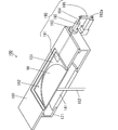
- FIG. 1 is a schematic sectional view showing the arrangement of an exposure apparatus according to the first embodiment of the present invention.
- FIG. 2 is a diagram for explaining the arrangement of the illuminance meter.
- FIG. 3 is a cross-sectional perspective view of the exposure apparatus.
- FIG. 4 is a longitudinal sectional view of the exposure apparatus.
- FIG. 5 is a graph showing the relationship between the oxygen concentration in the housing and the exhaust time.
- FIG. 6 is a graph showing the relationship between the illuminance of vacuum ultraviolet rays applied to the substrate by the light source unit and the lighting time of the light source unit.
- FIG. 7 is a functional block diagram showing the configuration of the control unit of FIG.
- FIG. 8 is a schematic diagram for explaining the operation of the exposure apparatus.
- FIG. 1 is a schematic sectional view showing the arrangement of an exposure apparatus according to the first embodiment of the present invention.
- FIG. 2 is a diagram for explaining the arrangement of the illuminance meter.
- FIG. 3 is a cross-section
- FIG. 9 is a schematic diagram for explaining the operation of the exposure apparatus.
- FIG. 10 is a schematic diagram for explaining the operation of the exposure apparatus.
- FIG. 11 is a schematic diagram for explaining the operation of the exposure apparatus.
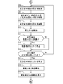
- FIG. 12 is a flowchart showing an example of an exposure process performed by the control unit of FIG.
- FIG. 13 is a flowchart showing an example of an exposure process performed by the control unit of FIG.
- FIG. 14 is a flowchart showing an example of exposure processing performed by the control unit of FIG.
- FIG. 15 is a schematic block diagram showing the overall configuration of a substrate processing apparatus provided with the exposure apparatus of FIG.
- FIG. 16 is a schematic view showing an example of substrate processing by the substrate processing apparatus of FIG. FIG.
- FIG. 17 is a cross-sectional perspective view of an exposure apparatus according to the second embodiment of the present invention.
- FIG. 18 is a longitudinal sectional view of the exposure apparatus of FIG.
- FIG. 19 is a cross-sectional perspective view of an exposure apparatus according to the third embodiment of the present invention.
- 20 is a longitudinal sectional view of the exposure apparatus of FIG.
- the term “substrate” refers to a semiconductor substrate, an FPD (Flat Panel Display) substrate such as a liquid crystal display device or an organic EL (Electro Luminescence) display device, an optical disk substrate, a magnetic disk substrate, and a magneto-optical disk. It refers to a substrate, a photomask substrate, a solar cell substrate, or the like.
- FIG. 1 is a schematic sectional view showing the arrangement of an exposure apparatus according to the first embodiment of the present invention.
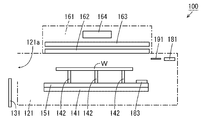
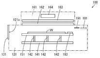
- the exposure apparatus 100 includes a control unit 110, a processing chamber 120, a closing unit 130, a delivery unit 140, an elevating unit 150, a light projecting unit 160, a replacement unit 170, a measuring unit 180, and a light shielding unit 190.
- the control unit 110 acquires measurement values from the measurement unit 180 and controls operations of the blocking unit 130, the lifting unit 150, the light projecting unit 160, the replacement unit 170, and the light shielding unit 190. The function of the control unit 110 will be described later.
- the processing chamber 120 includes a casing 121 having an upper opening and an internal space, an annular member 122, and a covering member 123.
- a transport opening 121 a for transporting the substrate W to be processed is formed between the inside and the outside of the housing 121.
- a film containing an induced self-organizing material hereinafter referred to as a DSA (Directed Self Assembly) film
- a connecting member 152 of an elevating unit 150 described later passes is formed on the bottom surface of the housing 121.
- the housing 161 of the light projecting unit 160 which will be described later, is disposed on the top of the housing 121 via the annular member 122, whereby the upper opening of the housing 121 is closed.
- Seal members s1 and s2 are attached between the casing 121 and the annular member 122 and between the annular member 122 and the housing 161, respectively.
- a covering member 123 is attached between the housing 121 and the housing 161 so as to cover the outer peripheral surface of the annular member 122.
- the closing part 130 includes a shutter 131, a rod-shaped connecting member 132, and a driving device 133.
- the connecting member 132 connects the shutter 131 and the driving device 133.
- the drive device 133 is a stepping motor, for example.
- the driving device 133 moves the shutter 131 between an open position where the shutter 131 opens the transport opening 121a and a closed position where the shutter 131 closes the transport opening 121a.
- a seal member 131 a is attached to the shutter 131.
- the inside of the housing 121 is hermetically sealed by the seal member 131a being in close contact with a portion of the housing 121 surrounding the transport opening 121a.
- the driving device 133 moves the shutter 131 away from the casing 121 when moving the shutter 131 between the open position and the closed position. Move up and down in the state.
- Position sensors 133a and 133b for detecting the upper limit position and the lower limit position of the shutter 131 are attached to the driving device 133.
- the position sensors 133a and 133b give the detection result to the control unit 110.
- the driving device 133 and driving devices 153 and 192 described later are provided outside the processing chamber 120. Therefore, even when dust is generated by driving the driving devices 133, 153, and 192, the dust is prevented from directly entering the housing 121.
- the delivery unit 140 includes, for example, a disk-shaped support plate 141 and a plurality (three in this example) of support pins 142.
- the support plate 141 is disposed in a horizontal posture within the housing 121.
- an opening 141a is formed through which a connecting member 152 of an elevating unit 150 described later passes.
- the plurality of support pins 142 extend upward from the upper surface of the support plate 141 so as to surround the opening 141a.
- the substrate W to be processed can be placed on the upper ends of the plurality of support pins 142.
- the elevating unit 150 includes a plate-shaped mounting plate 151, a rod-shaped connecting member 152, and a driving device 153.
- the mounting plate 151 is disposed in a horizontal posture above the support plate 141 of the delivery unit 140 in the housing 121.
- a plurality of through holes 151 a corresponding to the plurality of support pins 142 of the support plate 141 are formed in the mounting plate 151.
- the connecting member 152 is disposed to extend vertically through the opening 121 b of the housing 121 and the opening 141 a of the support plate 141, and the driving device 153 is disposed below the housing 121.
- the connecting member 152 connects the mounting plate 151 and the driving device 153.
- a seal member s3 is disposed between the outer peripheral surface of the connecting member 152 and the inner peripheral surface of the opening 121b so that the connecting member 152 can slide in the vertical direction.
- the driving device 153 is, for example, a stepping motor, and moves the mounting plate 151 between a processing position above the upper ends of the plurality of support pins 142 and a standby position below the upper ends of the plurality of support pins 142. Move up and down. In the state where the mounting plate 151 is in the standby position, the plurality of support pins 142 are inserted through the plurality of through holes 151a, respectively.
- Position sensors 153 a and 153 b for detecting the upper limit position and the lower limit position of the mounting plate 151 are attached to the driving device 153. The position sensors 153a and 153b give the detection result to the control unit 110.
- the light projecting unit 160 includes a housing 161 having a lower opening and an internal space, a translucent plate 162, a planar light source unit 163, and a power supply device 164.
- translucent plate 162 is a quartz glass plate.
- the housing 161 is disposed on the upper portion of the housing 121 so as to close the upper opening of the housing 121.
- the translucent plate 162 is attached to the housing 161 so as to close the lower opening of the housing 161.
- the internal space of the housing 121 and the internal space of the housing 161 are separated by a translucent plate 162 so as to be optically accessible.
- the light source unit 163 and the power supply device 164 are accommodated in the housing 161.
- the light source unit 163 is configured by horizontally arranging a plurality of rod-shaped light sources that emit vacuum ultraviolet rays having a wavelength of about 120 nm or more and about 230 nm or less at predetermined intervals.
- Each light source may be, for example, a xenon excimer lamp, or another excimer lamp or a deuterium lamp.
- the light source unit 163 emits vacuum ultraviolet rays having a substantially uniform light amount distribution in the housing 121 through the translucent plate 162.
- the area of the emission surface of the vacuum ultraviolet ray in the light source unit 163 is larger than the area of the surface to be processed of the substrate W.
- the power supply device 164 supplies power to the light source unit 163.
- the replacement unit 170 includes pipes 171p, 172p, 173p, valves 171v, 172v, and a suction device 173.
- the pipes 171p and 172p are connected between an air supply port of the casing 121 and an inert gas supply source.
- the inert gas is, for example, nitrogen gas.
- Valves 171v and 172v are inserted in the pipes 171p and 172p.
- the inert gas is supplied into the housing 121 from the side of the support plate 141 through the pipe 171p.
- An inert gas is supplied into the housing 121 from below the support plate 141 through the pipe 172p.
- the flow rate of the inert gas is adjusted by valves 171v and 172v.
- nitrogen gas is used as the inert gas.
- the pipe 173p branches into a branch pipe 173a and a branch pipe 173b.
- the branch pipe 173 a is connected to the exhaust port of the casing 121, and the end of the branch pipe 173 b is disposed between the casing 121 and the shutter 131.
- a suction device 173 is inserted in the pipe 173p.
- a valve 173v is inserted in the branch pipe 173b.
- the suction device 173 is, for example, an ejector.
- the pipe 173p is connected to the exhaust facility. The suction device 173 discharges the atmosphere in the housing 121 through the branch pipe 173a and the pipe 173p.
- the suction device 173 discharges the atmosphere between the housing 121 and the shutter 131 through the branch pipe 173b and the pipe 173p together with dust and the like generated by the movement of the shutter 131.
- the gas discharged by the suction device 173 is rendered harmless by the exhaust facility.
- the measuring unit 180 includes an oxygen concentration meter 181, an ozone concentration meter 182, and an illuminance meter 183.
- the oxygen concentration meter 181, the ozone concentration meter 182, and the illuminance meter 183 are connected to the control unit 110 through connection ports p 1, p 2, and p 3 provided in the housing 121.
- the oxygen concentration meter 181 is, for example, a galvanic cell type oxygen sensor or a zirconia type oxygen sensor, and measures the oxygen concentration in the housing 121.
- the ozone concentration meter 182 measures the ozone concentration in the housing 121.
- the illuminance meter 183 includes a light receiving element such as a photodiode, and measures the illuminance of vacuum ultraviolet rays from the light source unit 163 irradiated on the light receiving surface of the light receiving element.
- the illuminance is a work rate of vacuum ultraviolet rays irradiated per unit area of the light receiving surface.
- the unit of illuminance is represented by “W / m 2 ”, for example.
- the illuminance meter 183 is attached to the mounting plate 151 so that the light receiving surface of the light receiving element is positioned at substantially the same height as the surface to be processed of the substrate W.
- FIG. 2 is a diagram for explaining the arrangement of the illuminance meter 183.
- the translucent plate 162 has a rectangular shape, and the substrate W has a circular shape. Therefore, the vicinity of the corner portion of the translucent plate 162 does not overlap the substrate W at the processing position in plan view. Therefore, the mounting plate 151 includes a circular portion 151 b that overlaps the central portion of the light transmitting plate 162 and a corner portion 151 c that overlaps in the vicinity of one corner of the light transmitting plate 162 in plan view.
- the substrate W is placed on the circular portion 151b.
- the illuminometer 183 is attached to the corner 151c. According to this arrangement, the illuminance meter 183 can measure the illuminance of vacuum ultraviolet rays without interfering with the substrate W.
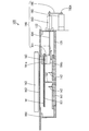
- FIG. 3 is a cross-sectional perspective view of the exposure apparatus 100 of FIG.
- FIG. 4 is a longitudinal sectional view of the exposure apparatus 100 of FIG. 3 and 4, some components are not shown in order to facilitate understanding of the internal configuration of the exposure apparatus 100.
- the light shielding portion 190 includes a light shielding member 191, a driving device 192, a guide portion 193, a rod-shaped support member 194, and a flat plate-shaped connection member 195.
- the drive device 192 is an air cylinder, for example, and has a drive shaft 192a that can advance and retreat in one direction.
- the driving device 192 is attached to the outer surface of the housing 121.
- the guide portion 193 is attached to the outer surface of the housing 121 and guides the support member 194 so as to be movable in a direction parallel to the forward / backward direction of the drive shaft 192a.
- the support member 194 is provided so as to penetrate the side wall of the housing 121 through the guide portion 193.
- the light shielding member 191 has an inverted L-shaped cross section composed of a horizontal plate 191a and a vertical plate 191b. The lower end of the vertical plate 191 b is attached to one end of the support member 194 in the housing 121.
- the connecting member 195 connects the other end of the support member 194 and the tip of the drive shaft 192 a of the drive device 192 outside the housing 121.
- the light shielding position is the position of the light shielding member 191 that shields the vacuum ultraviolet rays that the horizontal plate 191a irradiates the illuminance meter 183 from the light source unit 163.
- the non-light shielding position is a position of the light shielding member 191 where the horizontal plate 191a does not shield the vacuum ultraviolet rays irradiated from the light source unit 163 to the illuminance meter 183.
- the light shielding member 191 at the light shielding position is illustrated by a solid line
- the light shielding member 191 at the non-light shielding position is illustrated by an alternate long and short dash line.
- FIG. 5 is a graph showing the relationship between the oxygen concentration in the housing 121 and the exhaust time.
- the vertical axis in FIG. 5 indicates the oxygen concentration, and the horizontal axis indicates the exhaust time.
- the oxygen concentration in the housing 121 decreases as the exhaust time increases.
- time t0 when the oxygen concentration measured by the oxygen concentration meter 181 decreases to a predetermined exposure start concentration, irradiation of the vacuum ultraviolet rays from the light source unit 163 to the substrate W is started.
- the exposure start concentration is an oxygen concentration determined in advance so that vacuum ultraviolet rays can reach the substrate W from the light source unit 163 and ozone does not damage the film formed on the surface to be processed of the substrate W.
- the specific exposure start concentration differs depending on the type and components of the film formed on the substrate W to be processed, but is higher than the oxygen concentration of 1% at which almost no oxygen remains in the housing 121 and the atmosphere. Lower than the oxygen concentration inside.
- the oxygen concentration decreases to 1% at time t1.
- the irradiation of the vacuum ultraviolet rays is started at a time t0 that is earlier by ⁇ t than the time t1 when the oxygen concentration is reduced to 1%. Thereby, the time required for the exposure process can be shortened.
- the exposure amount of the vacuum ultraviolet rays applied to the substrate W by the light source unit 163 reaches a predetermined set exposure amount, the irradiation of the vacuum ultraviolet rays is stopped and the exposure process is ended.
- the exposure amount is the energy of vacuum ultraviolet rays irradiated per unit area of the surface to be processed of the substrate W during the exposure process.
- the unit of the exposure amount is represented by “J / m 2 ”, for example. Therefore, the exposure amount of vacuum ultraviolet rays is acquired by integrating the illuminance of vacuum ultraviolet rays measured by the illuminance meter 183.
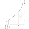
- FIG. 6 is a graph showing the relationship between the illuminance of the vacuum ultraviolet light emitted from the light source unit 163 and the lighting time of the light source unit 163.
- the vertical axis in FIG. 6 indicates the illuminance, and the horizontal axis indicates the lighting time.
- the light source of the light source unit 163 that emits vacuum ultraviolet rays is relatively expensive. Therefore, it is preferable to cut off the power supplied from the power supply device 164 to the light source unit 163 and turn off the light source unit 163 during a period when the substrate W is not irradiated with vacuum ultraviolet rays. Thereby, the lifetime of the light source part 163 can be prolonged.
- the illuminance of the vacuum ultraviolet rays applied to the substrate W decreases with time and converges to a constant value LV after a predetermined time. Therefore, it is difficult to measure the illuminance having a constant value LV before the exposure process.
- vacuum ultraviolet rays are simultaneously irradiated onto the substrate W and the illuminometer 183 during the exposure process. Therefore, when the illuminance of the vacuum ultraviolet rays applied to the substrate W changes, the illuminance of the vacuum ultraviolet rays measured by the illuminance meter 183 changes similarly.
- the illuminance meter 183 is provided such that the light receiving surface of the light receiving element is positioned at substantially the same height as the surface to be processed of the substrate W. Therefore, even when the vacuum ultraviolet rays are partially absorbed and attenuated by oxygen molecules remaining between the substrate W and the light source unit 163, the surface to be processed of the substrate W and the light receiving surface of the illuminometer 183 are approximately the same. Vacuum ultraviolet rays will arrive. The illuminance of the vacuum ultraviolet rays applied to the processing surface of the substrate W is equal to the illuminance measured by the illuminometer 183. As a result, the illuminance of the vacuum ultraviolet rays reaching the substrate W can be accurately measured with a simple configuration.
- the illuminance meter 183 On the other hand, if the illuminance meter 183 is continuously irradiated with vacuum ultraviolet rays for a long period of time, the illuminance meter 183 tends to deteriorate and the life of the illuminance meter 183 decreases. In addition, the frequency of performing maintenance work such as calibration of the illuminance meter 183 increases. In the present embodiment, the light shielding member 191 moves between the light shielding position and the non-light shielding position during the exposure process.
- the illuminometer 183 is intermittently irradiated with vacuum ultraviolet rays, and the deterioration rate of the illuminometer 183 is reduced as compared with the case where the illuminometer 183 is continuously irradiated with vacuum ultraviolet rays.
- the illuminance meter 183 extends its life. Further, the frequency of maintenance work of the illuminance meter 183 can be reduced.
- the illuminance of the vacuum ultraviolet rays applied to the substrate W is not measured during the period in which the light shielding member 191 is in the light shielding position (hereinafter referred to as the light shielding period). Therefore, it is preferable to interpolate the illuminance of the vacuum ultraviolet rays applied to the substrate W during the light shielding period. Interpolation of the illuminance during the light shielding period can be performed based on the illuminance measured by the illuminometer 183 before and after the light shielding period. For example, by connecting the illuminance values measured before and after the light shielding period with a spline curve, the illuminance during the light shielding period can be interpolated with a spline.
- FIG. 7 is a functional block diagram showing the configuration of the control unit 110 in FIG.
- the control unit 110 includes a blockage control unit 1, a lift control unit 2, an exhaust control unit 3, an air supply control unit 4, a concentration acquisition unit 5, a concentration comparison unit 6, a light shielding control unit 7, and illuminance acquisition.
- Unit 8 illuminance interpolation unit 9, exposure amount calculation unit 10, exposure amount comparison unit 11, and light projection control unit 12.
- the control unit 110 includes, for example, a CPU (Central Processing Unit) and a memory.
- a control program is stored in advance in the memory of the control unit 110.
- the function of each unit of the control unit 110 is realized by the CPU of the control unit 110 executing the control program stored in the memory.
- the closing control unit 1 controls the driving device 133 so that the shutter 131 moves between the closing position and the opening position based on the detection results of the position sensors 133a and 133b in FIG.
- the elevation control unit 2 controls the driving device 153 so that the mounting plate 151 moves between the standby position and the processing position based on the detection results of the position sensors 153a and 153b in FIG.
- the exhaust control unit 3 controls the suction device 173 and the valve 173v so as to exhaust the atmosphere in the casing 121 and the atmosphere between the casing 121 and the shutter 131 in FIG.
- the air supply control unit 4 controls the valves 171v and 172v in FIG. 1 so as to supply an inert gas into the housing 121.
- the concentration acquisition unit 5 acquires the value of the oxygen concentration measured by the oxygen concentration meter 181 of FIG.
- the concentration comparison unit 6 compares the oxygen concentration measured by the concentration acquisition unit 5 with the exposure start concentration.
- the light shielding control unit 7 controls the driving device 192 so that the light shielding member 191 in FIG. 4 reciprocates between the light shielding position and the non-light shielding position.
- the illuminance acquisition unit 8 acquires the illuminance value of vacuum ultraviolet rays measured by the illuminometer 183 in FIG.
- the illuminance interpolation unit 9 interpolates the illuminance of the vacuum ultraviolet rays irradiated to the substrate W during the light shielding period based on the control timing of the light shielding member 191 by the light shielding control unit 7 and the illuminance value acquired by the illuminance acquisition unit 8.
- the exposure amount calculation unit 10 illuminates the vacuum ultraviolet rays acquired by the illuminance acquisition unit 8, the illuminance of the vacuum ultraviolet rays interpolated by the illuminance interpolation unit 9, and the irradiation of the vacuum ultraviolet rays from the light source unit 163 in FIG. Based on the time, the exposure amount of the vacuum ultraviolet rays applied to the substrate W is calculated.
- the exposure amount comparison unit 11 compares the exposure amount calculated by the exposure amount calculation unit 10 with a predetermined set exposure amount.
- the light projection control unit 12 controls the supply of power from the power supply device 164 of FIG. 1 to the light source unit 163 so that the light source unit 163 emits vacuum ultraviolet rays based on the comparison result by the concentration comparison unit 6.
- the light projection control unit 12 supplies the exposure amount calculation unit 10 with the power supply time from the power supply device 164 to the light source unit 163 as the irradiation time of the vacuum ultraviolet rays from the light source unit 163 to the substrate W.
- the light projection control unit 12 controls the power supply device 164 so that the light source unit 163 stops the emission of the vacuum ultraviolet rays based on the comparison result by the exposure amount comparison unit 11.
- FIGS. 8 to 11 are schematic diagrams for explaining the operation of the exposure apparatus 100. 8 to 11, in order to facilitate understanding of the configurations in the casing 121 and the housing 161, some components are not shown, and the outlines of the casing 121 and the housing 161 are only one point. Indicated by a chain line. 12, 13 and 14 are flowcharts showing an example of the exposure process performed by the control unit 110 of FIG. Hereinafter, the exposure processing by the control unit 110 will be described with reference to FIGS.
- the shutter 131 in the initial state of the exposure process, the shutter 131 is in the closed position, the mounting plate 151 is in the standby position, and the light shielding member 191 is in the non-light shielding position.
- the oxygen concentration in the housing 121 is constantly or periodically measured by the oxygen concentration meter 181 and acquired by the concentration acquisition unit 5. At this time, the oxygen concentration in the housing 121 measured by the oxygen concentration meter 181 is equal to the oxygen concentration in the atmosphere.
- the closing control unit 1 moves the shutter 131 to the open position (step S1).
- the substrate W to be processed can be placed on the upper ends of the plurality of support pins 142 through the transport opening 121a.
- the substrate W is placed on the upper ends of the plurality of support pins 142 by the transfer device 220 shown in FIG.
- the elevation controller 2 determines whether or not the substrate W is placed on the upper ends of the plurality of support pins 142 (step S2). When the substrate W is not placed, the elevation control unit 2 waits until the substrate W is placed on the upper ends of the plurality of support pins 142. When the substrate W is placed, the elevating control unit 2 moves the shutter 131 to the closed position (step S3).
- the exhaust control unit 3 discharges the atmosphere in the housing 121 by the suction device 173 of FIG. 1 (step S4). Further, the air supply control unit 4 causes the inert gas to be supplied into the housing 121 through the pipes 171p and 172p in FIG. 1 (step S5). Either of the processes of steps S4 and S5 may be started first, or may be started simultaneously. Thereafter, as shown in FIG. 10, the elevation controller 2 raises the placement plate 151 from the standby position to place the substrate W on the placement plate 151 (step S ⁇ b> 6). At this time, the mounting surface of the substrate W and the light receiving surface of the illuminance meter 183 coincide with each other.
- the concentration comparison unit 6 determines whether or not the oxygen concentration in the casing 121 has decreased to the exposure start concentration (step S7).
- the concentration comparison unit 6 stands by until the oxygen concentration decreases to the exposure start concentration.
- the light projection control unit 12 causes the light source unit 163 to emit vacuum ultraviolet rays (step S8).
- vacuum ultraviolet rays are irradiated onto the substrate W from the light source unit 163 through the translucent plate 162, and exposure of the DSA film L3 formed on the surface to be processed is started.
- the raising / lowering control part 2 starts the raise of the mounting plate 151 (step S9).
- the illuminance acquisition unit 8 causes the illuminance meter 183 to start measuring the illuminance of vacuum ultraviolet rays, and acquires the measured illuminance from the illuminance meter 183 (step S10). Further, the light shielding control unit 7 reciprocates the light shielding member 191 a plurality of times between the light shielding position and the non-light shielding position (step S11). Any of the processes in steps S8 to S11 may be started first, or may be started simultaneously.
- the illuminance interpolation unit 9 interpolates the illuminance of the vacuum ultraviolet light during the light shielding period (step S12).
- the exposure amount calculation unit 10 calculates the exposure amount of the vacuum ultraviolet ray irradiated to the substrate W by integrating the illuminance of the vacuum ultraviolet ray acquired by the illuminance acquisition unit 8 and the illuminance of the vacuum ultraviolet ray interpolated by the illuminance interpolation unit 9. (Step S13).
- the elevation controller 2 determines whether or not the placement plate 151 has reached the processing position (step S14). When the mounting plate 151 has not reached the processing position, the elevation control unit 2 proceeds to the process of step S16. On the other hand, when the mounting plate 151 reaches the processing position, the elevation control unit 2 stops the lifting of the mounting plate 151 (step S15). As shown in FIG. 11, when the mounting plate 151 reaches the processing position, the substrate W comes close to the translucent plate 162.
- the exposure amount comparison unit 11 determines whether or not the exposure amount calculated by the exposure amount calculation unit 10 has reached the set exposure amount (step S16). If the exposure amount has not reached the set exposure amount, the exposure amount comparison unit 11 returns to the process of step S10. The processes in steps S10 to S16 are repeated until the exposure amount reaches the set exposure amount.
- the light projection control unit 12 stops the emission of the vacuum ultraviolet rays from the light source unit 163 (step S17).
- the illuminance acquisition unit 8 stops the measurement of illuminance by the illuminometer 183 (step S18).
- the light shielding control unit 7 stops the movement of the light shielding member 191 (step S19). In this example, the light shielding member 191 is returned to the non-light shielding position.
- the elevation controller 2 lowers the placement plate 151 to the standby position (step S20).
- the substrate W is transferred from the placement plate 151 to the plurality of support pins 142.
- the exhaust control unit 3 stops the discharge of the atmosphere in the housing 121 by the suction device 173 (step S21).
- the air supply control unit 4 stops the supply of inert gas from the pipes 171p and 172p into the housing 121 (step S22). Any of the processes in steps S17 to S22 may be started first, or may be started simultaneously.
- the closing control unit 1 moves the shutter 131 to the open position as shown in FIG. 9 (step S23).
- the exposed substrate W can be carried out from the plurality of support pins 142 to the outside of the housing 121 through the transport opening 121a.
- the substrate W is carried out from the plurality of support pins 142 to the outside of the housing 121 by the transfer device 220 shown in FIG.
- the closing control unit 1 determines whether or not the substrate W has been unloaded from the plurality of support pins 142 (step S24). When the substrate W has not been unloaded, the closing control unit 1 stands by until the substrate W is unloaded from the plurality of support pins 142. When the substrate W is carried out, the closing control unit 1 moves the shutter 131 to the closing position as shown in FIG. 8 (step S25), and ends the exposure process. By repeating the above operation, exposure processing can be sequentially performed on the plurality of substrates W.
- the substrate W is irradiated with vacuum ultraviolet rays from the light source unit 163 before the mounting plate 151 is moved to the processing position.
- the substrate W is irradiated with vacuum ultraviolet rays even in the process in which the mounting plate 151 moves from the standby position to the processing position. Therefore, the exposure of the substrate W is completed in a shorter time. Thereby, the efficiency of the exposure processing of the substrate W can be further improved.
- the substrate W may be irradiated with vacuum ultraviolet rays after the mounting plate 151 is moved to the processing position. That is, the processes of steps S9, S14, and S15 may be performed during the processes of steps S6 to S8, or may be performed simultaneously with the process of step S7.
- the mounting plate 151 can be moved to the standby position during a period in which the oxygen concentration in the housing 121 is reduced to the exposure start concentration. Therefore, the exposure of the substrate W is completed in a shorter time. Thereby, the efficiency of the exposure processing of the substrate W can be further improved.
- the placement plate 151 moves from the processing position to the standby position after the exposure amount of the substrate W reaches the set exposure amount, but the present invention is not limited to this.
- the mounting plate 151 may move from the processing position to the standby position before the exposure amount of the substrate W reaches the set exposure amount. That is, the process of step S20 may be executed before the process of step S16.
- the substrate W is irradiated with vacuum ultraviolet rays even in the process in which the mounting plate 151 moves from the processing position to the standby position. Therefore, the substrate W is unloaded from the processing chamber 120 at an earlier time point, and the exposure process ends. Thereby, the efficiency of the exposure processing of the substrate W can be further improved.
- FIG. 15 is a schematic block diagram showing the overall configuration of a substrate processing apparatus provided with the exposure apparatus 100 of FIG.
- processing using block copolymer induced self-assembly is performed.
- a processing liquid containing an induction self-organizing material is applied on the surface of the substrate W to be processed.
- two types of polymer patterns are formed on the surface to be processed of the substrate W by microphase separation that occurs in the induced self-assembled material.
- One of the two types of polymers is removed by the solvent.
- the treatment liquid containing the induced self-organizing material is called DSA liquid.
- DSA liquid a process for removing one of the two types of polymer patterns formed on the surface to be processed of the substrate W by microphase separation
- a developer a solvent used for the development process
- the substrate processing apparatus 200 includes a control device 210, a transport device 220, a heat treatment device 230, a coating device 240, and a developing device 250 in addition to the exposure device 100.
- the control device 210 includes, for example, a CPU and a memory or a microcomputer, and controls operations of the transport device 220, the heat treatment device 230, the coating device 240, and the developing device 250.
- the control device 210 gives a command for controlling the operation of the closing unit 130, the elevating unit 150, the light projecting unit 160, the replacement unit 170, and the light shielding unit 190 of the exposure apparatus 100 of FIG.
- the transport apparatus 220 transports the substrate W between the exposure apparatus 100, the heat treatment apparatus 230, the coating apparatus 240, and the development apparatus 250 while holding the substrate W to be processed.
- the heat treatment apparatus 230 heat-treats the substrate W before and after the coating process by the coating apparatus 240 and the development process by the developing apparatus 250.
- the coating apparatus 240 performs a film coating process by supplying a DSA liquid to the surface of the substrate W to be processed.
- a block copolymer composed of two types of polymers is used as the DSA liquid.
- Examples of combinations of two types of polymers include polystyrene-polymethyl methacrylate (PS-PMMA), polystyrene-polydimethylsiloxane (PS-PDMS), polystyrene-polyferrocenyldimethylsilane (PS-PFS), and polystyrene-polyethylene oxide.
- PS-PEO polystyrene-polyvinylpyridine
- PS-PHOST polystyrene-polyhydroxystyrene
- PMMA-PMAPOSS polymethyl methacrylate-polymethacrylate polyhedral oligomeric silsesquioxane
- the developing device 250 supplies the developer to the surface to be processed of the substrate W, thereby developing the film.
- a solvent for the developer for example, toluene, heptane, acetone, propylene glycol monomethyl ether acetate (PGMEA), propylene glycol monomethyl ether (PGME), cyclohexanone, acetic acid, tetrahydrofuran, isopropyl alcohol (IPA) or tetramethylammonium hydroxide (TMAH) ) And the like.
- FIG. 16 is a schematic diagram showing an example of processing of the substrate W by the substrate processing apparatus 200 of FIG.
- the state of the substrate W that changes each time processing is performed is shown in a cross-sectional view.
- the base layer L1 is formed so as to cover the surface to be processed of the substrate W as shown in FIG.
- a guide pattern L2 made of, for example, a photoresist is formed on L1.
- the operation of the substrate processing apparatus 200 will be described with reference to FIGS. 15 and 16.
- the transfer device 220 sequentially transfers the substrate W to be processed to the heat treatment device 230 and the coating device 240.
- the temperature of the substrate W is adjusted to a temperature suitable for forming the DSA film L3.
- the coating apparatus 240 the DSA liquid is supplied to the surface to be processed of the substrate W, and the coating process is performed. Accordingly, as shown in FIG. 16B, a DSA film L3 composed of two types of polymers is formed in a region on the base layer L1 where the guide pattern L2 is not formed.
- the transfer device 220 sequentially transfers the substrate W on which the DSA film L3 is formed to the heat treatment device 230 and the exposure device 100.
- the heat treatment apparatus 230 performs the heat treatment of the substrate W, thereby causing microphase separation in the DSA film L3.
- a pattern Q1 made of one polymer and a pattern Q2 made of the other polymer are formed.
- the linear pattern Q1 and the linear pattern Q2 are directionally formed along the guide pattern L2.
- the substrate W is cooled in the heat treatment apparatus 230. Further, in the exposure apparatus 100, the entire DSA film L3 after microphase separation is irradiated with vacuum ultraviolet rays for modifying the DSA film L3, and exposure processing is performed. Thereby, the bond between one polymer and the other polymer is cut, and the pattern Q1 and the pattern Q2 are separated.
- the transport device 220 sequentially transports the substrate W after the exposure processing by the exposure device 100 to the heat treatment device 230 and the developing device 250.
- the substrate W is cooled in the heat treatment apparatus 230.
- a developer is supplied to the DSA film L3 on the substrate W, and development processing is performed.
- the pattern Q1 is removed, and finally the pattern Q2 remains on the substrate W.
- the transport device 220 collects the substrate W after the development processing from the development device 250.
- FIG. 17 is a cross-sectional perspective view of an exposure apparatus according to the second embodiment of the present invention.
- FIG. 18 is a longitudinal sectional view of the exposure apparatus 100 of FIG. 17 and 18, some components are not shown in order to facilitate understanding of the internal configuration of the exposure apparatus 100.
- illuminance meter 183 is fixed to the inner side surface of casing 121 by fixing member 124.
- the illuminance meter 183 is arranged so that it overlaps in the vicinity of one corner of the translucent plate 162 in plan view, and the light receiving surface of the light receiving element is positioned at substantially the same height as the surface to be processed of the substrate W at the processing position.
- the placement plate 151 since the illuminance meter 183 is not attached to the placement plate 151, the placement plate 151 does not have the corner portion 151c of FIG. 2 for attaching the illuminance meter 183.
- the exposure apparatus 100 includes a light shielding unit 190A instead of the light shielding unit 190 of FIG.
- the light shielding unit 190A includes a light shielding member 191, a driving device 192, and a rod-shaped support member 194.
- the light shielding member 191 is, for example, a shutter, and is provided so as to be movable between a light shielding position that shields vacuum ultraviolet rays irradiated from the light source unit 163 to the illuminance meter 183 and a non-light shielding position that does not shield vacuum ultraviolet rays.
- the driving device 192 is a stepping motor, for example, and has a rotatable driving shaft 192a.
- the drive device 192 is attached to the lower surface of the housing 121 so that the drive shaft 192a faces upward.
- the support member 194 connects the light shielding member 191 and the drive shaft 192a of the drive device 192 so as to extend in the vertical direction.
- the drive shaft 192a of the drive device 192 rotates around an axis parallel to the vertical direction, the light shielding member 191 moves between the light shielding position and the non-light shielding position.
- the illuminance meter 183 does not move in the vertical direction. Therefore, in the exposure process, after the substrate W is moved to the processing position and the surface to be processed of the substrate W and the light receiving surface of the light receiving element of the illuminance meter 183 have substantially the same height, the vacuum ultraviolet ray is emitted from the light source unit 163. Is preferably emitted. Therefore, in the exposure process in the present embodiment, it is preferable that the processes of steps S9, S14, and S15 of FIGS. 12 to 14 are executed during the processes of steps S6 to S8.
- FIG. 19 is a cross-sectional perspective view of an exposure apparatus according to the third embodiment of the present invention.
- FIG. 20 is a longitudinal sectional view of the exposure apparatus 100 of FIG. 19 and 20, some components are not shown in order to facilitate understanding of the internal configuration of the exposure apparatus 100.
- the exposure apparatus 100 includes a light shielding unit 190B instead of the light shielding unit 190 of FIG.
- the light shielding part 190B has the same configuration as the light shielding part 190 of FIG. 3 except that the light shielding member 191 is not included.
- the support member 194 supports the illuminance meter 183 with one end instead of the light shielding member 191.
- the illuminance meter 183 is not attached to the placement plate 151, and therefore the placement plate 151 is attached to the corner portion 151c of FIG. 2 for attaching the illuminance meter 183. Does not have.
- the illuminance meter 183 is between a non-light-shielding position where vacuum ultraviolet rays can be received and a light-shielding position where vacuum ultraviolet rays cannot be received.
- the illuminance meter 183 at the non-light-shielding position is illustrated by a solid line
- the illuminance meter 183 at the light-shielding position is illustrated by a one-dot chain line.
- the non-light-shielding position is a position that overlaps with the vicinity of one corner of the translucent plate 162 in plan view.
- the light shielding position is a position outside the translucent plate 162 in plan view.
- the illuminometer 183 instead of the light shielding member 191 moves between the non-light shielding position and the light shielding position during the exposure process. Therefore, in the exposure processing of the present embodiment, the illuminance meter 183 instead of the light shielding member 191 is moved between the non-light shielding position and the light shielding position in step S11 of FIG. Further, in step S19 of FIG. 13, the movement of the illuminance meter 183 instead of the light shielding member 191 is stopped.
- the illuminance interpolation method in the non-light-receiving period of the present embodiment is the same as the illuminance interpolation method in the light-shielding period of the first embodiment.
- the illuminance meter 183 does not move in the vertical direction, as in the second embodiment. Therefore, in the exposure process, after the substrate W is moved to the processing position and the surface to be processed of the substrate W and the light receiving surface of the light receiving element of the illuminance meter 183 have substantially the same height, the vacuum ultraviolet ray is emitted from the light source unit 163. Is preferably emitted. Therefore, in the exposure process in the present embodiment, it is preferable that the processes of steps S9, S14, and S15 of FIGS. 12 to 14 are executed during the processes of steps S6 to S8.
- the DSA liquid is used as the processing liquid, but the present invention is not limited to this. Other processing liquids different from the DSA liquid may be used.
- the exit surface of the vacuum ultraviolet ray is larger than the surface to be processed of the substrate W, and the entire surface of the substrate W is exposed, but the present invention is not limited to this.
- the emission surface of the vacuum ultraviolet light may be smaller than the surface to be processed of the substrate W, or the planar vacuum ultraviolet light may not be emitted.
- the vacuum ultraviolet ray is irradiated on the entire surface of the substrate W to be processed by relatively moving the vacuum ultraviolet ray emitting surface and the surface of the substrate W to be processed.
- an inert gas is supplied into the housing 121 during the exposure process, but the present invention is not limited to this. If the oxygen concentration in the housing 121 can be sufficiently reduced during the exposure processing, the inert gas may not be supplied into the housing 121.
- the translucent plate 162 has a rectangular shape, but the present invention is not limited to this.
- the translucent plate 162 may have other shapes such as a polygonal shape other than a rectangular shape, a circular shape, an oval shape, or an elliptical shape.
- the illuminance meter 183 is disposed at a position overlapping the non-overlapping region between the translucent plate 162 and the surface to be processed of the substrate W in plan view. Thereby, the illuminance meter 183 can measure the illuminance of the vacuum ultraviolet rays without interfering with the substrate W.
- the illuminometer 183 is attached to the mounting plate 151, but the present invention is not limited to this. As long as the illuminance meter 183 can move up and down following the movement of the mounting plate 151, the illuminance meter 183 may not be attached to the mounting plate 151. In this case, the illuminance meter 183 may be configured to be movable by a driving device 153 common to the mounting plate 151, or may be configured to be movable by a driving device different from the driving device 153.
- the light shielding unit 190A is provided in the exposure apparatus 100, but the present invention is not limited to this.
- the exposure apparatus 100 may be provided with a light shielding part 190 similar to that of the first embodiment instead of the light shielding part 190A.
- the illuminometer 183 is fixed and the light shielding member 191 is configured to be movable by the driving device 192.
- the present invention is not limited to this.
- the light shielding member 191 may be fixed, and the illuminance meter 183 may be configured to be movable by the driving device 192. That is, the illuminance meter 183 and the light shielding member 191 need only be relatively movable.
- a position where the illuminance meter 183 and the light shielding member 191 overlap in a plan view is a light shielding position
- a position where the illuminance meter 183 and the light shielding member 191 do not overlap in a plan view is a non-light shielding position
- the light shielding member 191 may be fixed and the illuminance meter 183 may be configured to be movable by the driving device 192.
- the corner portion 151c of the mounting plate 151 to which the illuminance meter 183 is attached is configured to be movable in a horizontal plane independently of the circular portion 151b.
- the illuminance meter 183 is arranged so that the light receiving surface is substantially the same height as the surface to be processed of the substrate W at the processing position. It is not limited to.
- the illuminometer 183 may be arranged such that the light receiving surface is located at a certain height with respect to the surface to be processed of the substrate W at the processing position. Further, when the illuminance meter 183 can measure the illuminance of the vacuum ultraviolet rays with sufficient accuracy, the vacuum applied to the substrate W in the process of being moved to the processing position in the second and third embodiments. Ultraviolet rays may be measured.
- the irradiation of the vacuum ultraviolet rays from the light source unit 163 to the substrate W is started when the oxygen concentration is lowered to the exposure start concentration.
- the present invention is not limited to this.
- the irradiation of the vacuum ultraviolet rays from the light source unit 163 to the substrate W may be started when the oxygen concentration is lowered to an oxygen concentration lower than the exposure start concentration (for example, an oxygen concentration at which ozone is not generated).
- the illuminance is interpolated in the light shielding period, but the present invention is not limited to this. Interpolation of illuminance during the light shielding period may not be performed. Therefore, the control unit 110 may not include the light shielding control unit 7 and the illuminance interpolation unit 9.
- the substrate W is an example of a substrate
- the light projecting unit 160 is an example of a light projecting unit
- the illuminance meter 183 is an example of an illuminance meter
- the light shielding units 190, 190A, 190B are light shielding units.
- the light projection control unit 12 is an example of a light projection control unit
- the exposure apparatus 100 is an example of an exposure apparatus
- the light shielding member 191 is an example of a light shielding member
- the driving device 192 is a first or second driving unit.
- the translucent plate 162 is an example of an emitting part.
- the processing chamber 120 is an example of a processing chamber
- the mounting plate 151 is an example of a mounting unit
- the elevation control unit 2 is an example of a mounting control unit
- the circular portion 151b is an example of a first part.
- the circular portion 151b is an example of the second portion.
- the coating device 240 is an example of a coating processing unit
- the thermal processing device 230 is an example of a thermal processing unit
- the developing device 250 is an example of a developing processing unit
- the substrate processing device 200 is an example of a substrate processing device.
Landscapes
- Physics & Mathematics (AREA)
- General Physics & Mathematics (AREA)
- Engineering & Computer Science (AREA)
- Condensed Matter Physics & Semiconductors (AREA)
- Manufacturing & Machinery (AREA)
- Computer Hardware Design (AREA)
- Microelectronics & Electronic Packaging (AREA)
- Power Engineering (AREA)
- Plasma & Fusion (AREA)
- Exposure And Positioning Against Photoresist Photosensitive Materials (AREA)
- Exposure Of Semiconductors, Excluding Electron Or Ion Beam Exposure (AREA)
Abstract
Selon l'invention, un dispositif d'exposition (100) comprend une unité de projection de lumière (160), un luxmètre (183), une unité de protection contre la lumière (190) et une unité de commande de projection de lumière (12). Un rayonnement ultraviolet du vide est projeté, par l'unité de projection de lumière, sur une surface à traiter d'un substrat (W). Dans une période de projection du rayonnement ultraviolet du vide de l'unité de projection de lumière sur le substrat, une partie du rayonnement ultraviolet du vide est reçue par le luxmètre, et l'éclairement du rayonnement ultraviolet du vide reçu est mesuré. Dans la période de projection, l'effet du rayonnement ultraviolet du vide sur une surface de réception de lumière du luxmètre est bloqué par intermittence par l'unité de protection contre la lumière. En fonction de l'éclairement mesuré en utilisant le luxmètre, la projection sur le substrat du rayonnement ultraviolet du vide par l'unité de projection de lumière est arrêtée.
Priority Applications (2)
| Application Number | Priority Date | Filing Date | Title |
|---|---|---|---|
| KR1020197023927A KR102307596B1 (ko) | 2017-03-01 | 2017-10-04 | 노광 장치, 기판 처리 장치, 기판의 노광 방법 및 기판 처리 방법 |
| CN201780077239.0A CN110100301B (zh) | 2017-03-01 | 2017-10-04 | 曝光装置、衬底处理装置、衬底曝光方法及衬底处理方法 |
Applications Claiming Priority (2)
| Application Number | Priority Date | Filing Date | Title |
|---|---|---|---|
| JP2017-038236 | 2017-03-01 | ||
| JP2017038236A JP6768561B2 (ja) | 2017-03-01 | 2017-03-01 | 露光装置、基板処理装置、基板の露光方法および基板処理方法 |
Publications (1)
| Publication Number | Publication Date |
|---|---|
| WO2018159005A1 true WO2018159005A1 (fr) | 2018-09-07 |
Family
ID=63370897
Family Applications (1)
| Application Number | Title | Priority Date | Filing Date |
|---|---|---|---|
| PCT/JP2017/036074 WO2018159005A1 (fr) | 2017-03-01 | 2017-10-04 | Dispositif d'exposition, dispositif de traitement de substrat, procédé d'exposition de substrat, et procédé de traitement de substrat |
Country Status (5)
| Country | Link |
|---|---|
| JP (1) | JP6768561B2 (fr) |
| KR (1) | KR102307596B1 (fr) |
| CN (1) | CN110100301B (fr) |
| TW (1) | TWI649642B (fr) |
| WO (1) | WO2018159005A1 (fr) |
Cited By (2)
| Publication number | Priority date | Publication date | Assignee | Title |
|---|---|---|---|---|
| US20200383200A1 (en) * | 2019-05-30 | 2020-12-03 | Kla Corporation | Optical Etendue Matching Methods for Extreme Ultraviolet Metrology |
| CN112526827A (zh) * | 2019-09-19 | 2021-03-19 | 株式会社斯库林集团 | 曝光装置 |
Citations (6)
| Publication number | Priority date | Publication date | Assignee | Title |
|---|---|---|---|---|
| JPH05343288A (ja) * | 1992-06-11 | 1993-12-24 | Nikon Corp | 露光装置 |
| JPH10284407A (ja) * | 1997-04-08 | 1998-10-23 | Nikon Corp | 露光装置及び露光装置を用いた半導体デバイスの製造方法 |
| JP2001110710A (ja) * | 1999-10-08 | 2001-04-20 | Nikon Corp | 露光装置、露光方法、および半導体デバイスの製造方法 |
| JP2006049730A (ja) * | 2004-08-06 | 2006-02-16 | Sharp Corp | 露光装置、露光量制御方法、露光量制御プログラムとその記録媒体 |
| JP2015222417A (ja) * | 2014-04-28 | 2015-12-10 | 株式会社ブイ・テクノロジー | 露光装置及び露光方法 |
| JP2016183990A (ja) * | 2015-03-25 | 2016-10-20 | 株式会社Screenホールディングス | 露光装置、基板処理装置、基板の露光方法および基板処理方法 |
Family Cites Families (10)
| Publication number | Priority date | Publication date | Assignee | Title |
|---|---|---|---|---|
| JPH10229038A (ja) * | 1997-02-14 | 1998-08-25 | Nikon Corp | 露光量制御方法 |
| AU8358198A (en) * | 1997-07-25 | 1999-02-16 | Nikon Corporation | Projection aligner, projection exposure method, optical cleaning method and method of fabricating semiconductor device |
| JPH11251220A (ja) * | 1998-03-02 | 1999-09-17 | Nikon Corp | 露光装置及び露光方法 |
| JP2000100685A (ja) * | 1998-09-17 | 2000-04-07 | Nikon Corp | 露光装置及び該装置を用いた露光方法 |
| US6211942B1 (en) * | 2000-03-10 | 2001-04-03 | Howa Machinery Ltd. | Double-sided exposure system |
| WO2006006730A1 (fr) * | 2004-07-15 | 2006-01-19 | Nikon Corporation | Équipement pour moteur planaire, équipement à étages, équipement d’exposition et méthode de fabrication du dispositif |
| JP4491445B2 (ja) * | 2005-11-04 | 2010-06-30 | 株式会社オーク製作所 | 周辺露光装置およびその方法 |
| JP4859660B2 (ja) * | 2006-12-27 | 2012-01-25 | 東京応化工業株式会社 | 基板処置装置 |
| JP2013104934A (ja) * | 2011-11-11 | 2013-05-30 | Tokyo Electron Ltd | 露光装置及び露光方法 |
| JP6495707B2 (ja) * | 2015-03-25 | 2019-04-03 | 株式会社Screenホールディングス | 露光装置および基板処理装置 |
-
2017
- 2017-03-01 JP JP2017038236A patent/JP6768561B2/ja active Active
- 2017-10-04 KR KR1020197023927A patent/KR102307596B1/ko active IP Right Grant
- 2017-10-04 CN CN201780077239.0A patent/CN110100301B/zh active Active
- 2017-10-04 WO PCT/JP2017/036074 patent/WO2018159005A1/fr active Application Filing
- 2017-10-18 TW TW106135708A patent/TWI649642B/zh active
Patent Citations (6)
| Publication number | Priority date | Publication date | Assignee | Title |
|---|---|---|---|---|
| JPH05343288A (ja) * | 1992-06-11 | 1993-12-24 | Nikon Corp | 露光装置 |
| JPH10284407A (ja) * | 1997-04-08 | 1998-10-23 | Nikon Corp | 露光装置及び露光装置を用いた半導体デバイスの製造方法 |
| JP2001110710A (ja) * | 1999-10-08 | 2001-04-20 | Nikon Corp | 露光装置、露光方法、および半導体デバイスの製造方法 |
| JP2006049730A (ja) * | 2004-08-06 | 2006-02-16 | Sharp Corp | 露光装置、露光量制御方法、露光量制御プログラムとその記録媒体 |
| JP2015222417A (ja) * | 2014-04-28 | 2015-12-10 | 株式会社ブイ・テクノロジー | 露光装置及び露光方法 |
| JP2016183990A (ja) * | 2015-03-25 | 2016-10-20 | 株式会社Screenホールディングス | 露光装置、基板処理装置、基板の露光方法および基板処理方法 |
Cited By (3)
| Publication number | Priority date | Publication date | Assignee | Title |
|---|---|---|---|---|
| US20200383200A1 (en) * | 2019-05-30 | 2020-12-03 | Kla Corporation | Optical Etendue Matching Methods for Extreme Ultraviolet Metrology |
| US11968772B2 (en) * | 2019-05-30 | 2024-04-23 | Kla Corporation | Optical etendue matching methods for extreme ultraviolet metrology |
| CN112526827A (zh) * | 2019-09-19 | 2021-03-19 | 株式会社斯库林集团 | 曝光装置 |
Also Published As
| Publication number | Publication date |
|---|---|
| CN110100301A (zh) | 2019-08-06 |
| JP2018147918A (ja) | 2018-09-20 |
| CN110100301B (zh) | 2023-07-21 |
| JP6768561B2 (ja) | 2020-10-14 |
| KR102307596B1 (ko) | 2021-09-30 |
| KR20190102289A (ko) | 2019-09-03 |
| TWI649642B (zh) | 2019-02-01 |
| TW201833670A (zh) | 2018-09-16 |
Similar Documents
| Publication | Publication Date | Title |
|---|---|---|
| KR101764534B1 (ko) | 노광 장치, 기판 처리 장치, 기판의 노광 방법 및 기판 처리 방법 | |
| KR101846652B1 (ko) | 노광 장치 및 기판 처리 장치 | |
| TWI706226B (zh) | 曝光裝置、基板處理裝置、基板之曝光方法及基板處理方法 | |
| TWI659275B (zh) | 曝光裝置、基板處理裝置、曝光方法、及基板處理方法 | |
| TWI666525B (zh) | 曝光裝置及基板處理裝置 | |
| WO2018159005A1 (fr) | Dispositif d'exposition, dispositif de traitement de substrat, procédé d'exposition de substrat, et procédé de traitement de substrat | |
| WO2018173344A1 (fr) | Dispositif d'exposition, dispositif de traitement de substrats, procédé d'exposition de substrats, et procédé de traitement de substrats | |
| WO2018190273A1 (fr) | Dispositif d'exposition, dispositif de traitement de substrat, procédé d'exposition de substrat, et procédé de traitement de substrat | |
| TWI682433B (zh) | 曝光裝置、基板處理裝置、基板曝光方法以及基板處理方法 | |
| JP6924661B2 (ja) | 露光装置、基板処理装置、露光方法および基板処理方法 | |
| JP2019057641A (ja) | 露光装置、基板処理装置、露光方法および基板処理方法 | |
| JP3333068B2 (ja) | 基板処理装置 |
Legal Events
| Date | Code | Title | Description |
|---|---|---|---|
| 121 | Ep: the epo has been informed by wipo that ep was designated in this application |
Ref document number: 17898755 Country of ref document: EP Kind code of ref document: A1 |
|
| ENP | Entry into the national phase |
Ref document number: 20197023927 Country of ref document: KR Kind code of ref document: A |
|
| NENP | Non-entry into the national phase |
Ref country code: DE |
|
| 122 | Ep: pct application non-entry in european phase |
Ref document number: 17898755 Country of ref document: EP Kind code of ref document: A1 |