KR102307596B1 - 노광 장치, 기판 처리 장치, 기판의 노광 방법 및 기판 처리 방법 - Google Patents
노광 장치, 기판 처리 장치, 기판의 노광 방법 및 기판 처리 방법 Download PDFInfo
- Publication number
- KR102307596B1 KR102307596B1 KR1020197023927A KR20197023927A KR102307596B1 KR 102307596 B1 KR102307596 B1 KR 102307596B1 KR 1020197023927 A KR1020197023927 A KR 1020197023927A KR 20197023927 A KR20197023927 A KR 20197023927A KR 102307596 B1 KR102307596 B1 KR 102307596B1
- Authority
- KR
- South Korea
- Prior art keywords
- substrate
- light
- vacuum ultraviolet
- unit
- ultraviolet rays
- Prior art date
Links
- 239000000758 substrate Substances 0.000 title claims abstract description 251
- 238000012545 processing Methods 0.000 title claims description 102
- 238000000034 method Methods 0.000 title claims description 76
- 238000003672 processing method Methods 0.000 title description 6
- 230000000903 blocking effect Effects 0.000 claims abstract description 77
- 238000010438 heat treatment Methods 0.000 claims description 23
- 239000007788 liquid Substances 0.000 claims description 18
- 238000000576 coating method Methods 0.000 claims description 16
- 239000011248 coating agent Substances 0.000 claims description 14
- 239000000463 material Substances 0.000 claims description 10
- 230000001678 irradiating effect Effects 0.000 claims description 9
- 239000002904 solvent Substances 0.000 claims description 8
- QVGXLLKOCUKJST-UHFFFAOYSA-N atomic oxygen Chemical compound [O] QVGXLLKOCUKJST-UHFFFAOYSA-N 0.000 description 41
- 239000001301 oxygen Substances 0.000 description 41
- 229910052760 oxygen Inorganic materials 0.000 description 41
- 238000002408 directed self-assembly Methods 0.000 description 21
- 230000007423 decrease Effects 0.000 description 15
- 239000011261 inert gas Substances 0.000 description 12
- 229920000642 polymer Polymers 0.000 description 12
- 238000010586 diagram Methods 0.000 description 11
- CBENFWSGALASAD-UHFFFAOYSA-N Ozone Chemical compound [O-][O+]=O CBENFWSGALASAD-UHFFFAOYSA-N 0.000 description 7
- 239000012528 membrane Substances 0.000 description 7
- KFZMGEQAYNKOFK-UHFFFAOYSA-N Isopropanol Chemical compound CC(C)O KFZMGEQAYNKOFK-UHFFFAOYSA-N 0.000 description 6
- 230000006866 deterioration Effects 0.000 description 6
- 238000000926 separation method Methods 0.000 description 6
- 238000005259 measurement Methods 0.000 description 5
- 238000001514 detection method Methods 0.000 description 4
- 230000002452 interceptive effect Effects 0.000 description 4
- 238000012423 maintenance Methods 0.000 description 4
- WGTYBPLFGIVFAS-UHFFFAOYSA-M tetramethylammonium hydroxide Chemical compound [OH-].C[N+](C)(C)C WGTYBPLFGIVFAS-UHFFFAOYSA-M 0.000 description 4
- 238000012546 transfer Methods 0.000 description 4
- QTBSBXVTEAMEQO-UHFFFAOYSA-N Acetic acid Chemical compound CC(O)=O QTBSBXVTEAMEQO-UHFFFAOYSA-N 0.000 description 3
- CSCPPACGZOOCGX-UHFFFAOYSA-N Acetone Chemical compound CC(C)=O CSCPPACGZOOCGX-UHFFFAOYSA-N 0.000 description 3
- YXFVVABEGXRONW-UHFFFAOYSA-N Toluene Chemical compound CC1=CC=CC=C1 YXFVVABEGXRONW-UHFFFAOYSA-N 0.000 description 3
- 229920001400 block copolymer Polymers 0.000 description 3
- 238000011161 development Methods 0.000 description 3
- 239000000428 dust Substances 0.000 description 3
- 230000006870 function Effects 0.000 description 3
- 230000002093 peripheral effect Effects 0.000 description 3
- 238000007789 sealing Methods 0.000 description 3
- XLYOFNOQVPJJNP-UHFFFAOYSA-N water Substances O XLYOFNOQVPJJNP-UHFFFAOYSA-N 0.000 description 3
- ARXJGSRGQADJSQ-UHFFFAOYSA-N 1-methoxypropan-2-ol Chemical compound COCC(C)O ARXJGSRGQADJSQ-UHFFFAOYSA-N 0.000 description 2
- IJGRMHOSHXDMSA-UHFFFAOYSA-N Atomic nitrogen Chemical compound N#N IJGRMHOSHXDMSA-UHFFFAOYSA-N 0.000 description 2
- IMNFDUFMRHMDMM-UHFFFAOYSA-N N-Heptane Chemical compound CCCCCCC IMNFDUFMRHMDMM-UHFFFAOYSA-N 0.000 description 2
- WYURNTSHIVDZCO-UHFFFAOYSA-N Tetrahydrofuran Chemical compound C1CCOC1 WYURNTSHIVDZCO-UHFFFAOYSA-N 0.000 description 2
- MCMNRKCIXSYSNV-UHFFFAOYSA-N Zirconium dioxide Chemical compound O=[Zr]=O MCMNRKCIXSYSNV-UHFFFAOYSA-N 0.000 description 2
- 230000002238 attenuated effect Effects 0.000 description 2
- 230000015572 biosynthetic process Effects 0.000 description 2
- 230000001276 controlling effect Effects 0.000 description 2
- 230000000875 corresponding effect Effects 0.000 description 2
- JHIVVAPYMSGYDF-UHFFFAOYSA-N cyclohexanone Chemical compound O=C1CCCCC1 JHIVVAPYMSGYDF-UHFFFAOYSA-N 0.000 description 2
- 230000003247 decreasing effect Effects 0.000 description 2
- 229910001873 dinitrogen Inorganic materials 0.000 description 2
- 238000005401 electroluminescence Methods 0.000 description 2
- 230000006698 induction Effects 0.000 description 2
- 125000004430 oxygen atom Chemical group O* 0.000 description 2
- 238000000206 photolithography Methods 0.000 description 2
- LLHKCFNBLRBOGN-UHFFFAOYSA-N propylene glycol methyl ether acetate Chemical compound COCC(C)OC(C)=O LLHKCFNBLRBOGN-UHFFFAOYSA-N 0.000 description 2
- YZCKVEUIGOORGS-OUBTZVSYSA-N Deuterium Chemical compound [2H] YZCKVEUIGOORGS-OUBTZVSYSA-N 0.000 description 1
- 229920003171 Poly (ethylene oxide) Polymers 0.000 description 1
- VYPSYNLAJGMNEJ-UHFFFAOYSA-N Silicium dioxide Chemical compound O=[Si]=O VYPSYNLAJGMNEJ-UHFFFAOYSA-N 0.000 description 1
- 238000013459 approach Methods 0.000 description 1
- 230000002596 correlated effect Effects 0.000 description 1
- 229910052805 deuterium Inorganic materials 0.000 description 1
- 239000004205 dimethyl polysiloxane Substances 0.000 description 1
- 230000000694 effects Effects 0.000 description 1
- 230000003028 elevating effect Effects 0.000 description 1
- 239000007789 gas Substances 0.000 description 1
- 238000005286 illumination Methods 0.000 description 1
- 239000004973 liquid crystal related substance Substances 0.000 description 1
- JESXATFQYMPTNL-UHFFFAOYSA-N mono-hydroxyphenyl-ethylene Natural products OC1=CC=CC=C1C=C JESXATFQYMPTNL-UHFFFAOYSA-N 0.000 description 1
- 230000003287 optical effect Effects 0.000 description 1
- 229920002120 photoresistant polymer Polymers 0.000 description 1
- 229920000435 poly(dimethylsiloxane) Polymers 0.000 description 1
- 229920005590 poly(ferrocenyl dimethylsilane) Polymers 0.000 description 1
- 229920003229 poly(methyl methacrylate) Polymers 0.000 description 1
- 229920000193 polymethacrylate Polymers 0.000 description 1
- 239000004926 polymethyl methacrylate Substances 0.000 description 1
- 229920002717 polyvinylpyridine Polymers 0.000 description 1
- 230000002035 prolonged effect Effects 0.000 description 1
- 238000001338 self-assembly Methods 0.000 description 1
- 239000004065 semiconductor Substances 0.000 description 1
- YLQBMQCUIZJEEH-UHFFFAOYSA-N tetrahydrofuran Natural products C=1C=COC=1 YLQBMQCUIZJEEH-UHFFFAOYSA-N 0.000 description 1
- 229910052724 xenon Inorganic materials 0.000 description 1
- FHNFHKCVQCLJFQ-UHFFFAOYSA-N xenon atom Chemical compound [Xe] FHNFHKCVQCLJFQ-UHFFFAOYSA-N 0.000 description 1
Images


Classifications
-
- G—PHYSICS
- G03—PHOTOGRAPHY; CINEMATOGRAPHY; ANALOGOUS TECHNIQUES USING WAVES OTHER THAN OPTICAL WAVES; ELECTROGRAPHY; HOLOGRAPHY
- G03F—PHOTOMECHANICAL PRODUCTION OF TEXTURED OR PATTERNED SURFACES, e.g. FOR PRINTING, FOR PROCESSING OF SEMICONDUCTOR DEVICES; MATERIALS THEREFOR; ORIGINALS THEREFOR; APPARATUS SPECIALLY ADAPTED THEREFOR
- G03F7/00—Photomechanical, e.g. photolithographic, production of textured or patterned surfaces, e.g. printing surfaces; Materials therefor, e.g. comprising photoresists; Apparatus specially adapted therefor
- G03F7/20—Exposure; Apparatus therefor
- G03F7/2002—Exposure; Apparatus therefor with visible light or UV light, through an original having an opaque pattern on a transparent support, e.g. film printing, projection printing; by reflection of visible or UV light from an original such as a printed image
- G03F7/2004—Exposure; Apparatus therefor with visible light or UV light, through an original having an opaque pattern on a transparent support, e.g. film printing, projection printing; by reflection of visible or UV light from an original such as a printed image characterised by the use of a particular light source, e.g. fluorescent lamps or deep UV light
-
- G—PHYSICS
- G03—PHOTOGRAPHY; CINEMATOGRAPHY; ANALOGOUS TECHNIQUES USING WAVES OTHER THAN OPTICAL WAVES; ELECTROGRAPHY; HOLOGRAPHY
- G03F—PHOTOMECHANICAL PRODUCTION OF TEXTURED OR PATTERNED SURFACES, e.g. FOR PRINTING, FOR PROCESSING OF SEMICONDUCTOR DEVICES; MATERIALS THEREFOR; ORIGINALS THEREFOR; APPARATUS SPECIALLY ADAPTED THEREFOR
- G03F7/00—Photomechanical, e.g. photolithographic, production of textured or patterned surfaces, e.g. printing surfaces; Materials therefor, e.g. comprising photoresists; Apparatus specially adapted therefor
- G03F7/20—Exposure; Apparatus therefor
-
- G—PHYSICS
- G03—PHOTOGRAPHY; CINEMATOGRAPHY; ANALOGOUS TECHNIQUES USING WAVES OTHER THAN OPTICAL WAVES; ELECTROGRAPHY; HOLOGRAPHY
- G03F—PHOTOMECHANICAL PRODUCTION OF TEXTURED OR PATTERNED SURFACES, e.g. FOR PRINTING, FOR PROCESSING OF SEMICONDUCTOR DEVICES; MATERIALS THEREFOR; ORIGINALS THEREFOR; APPARATUS SPECIALLY ADAPTED THEREFOR
- G03F7/00—Photomechanical, e.g. photolithographic, production of textured or patterned surfaces, e.g. printing surfaces; Materials therefor, e.g. comprising photoresists; Apparatus specially adapted therefor
- G03F7/26—Processing photosensitive materials; Apparatus therefor
- G03F7/38—Treatment before imagewise removal, e.g. prebaking
-
- G—PHYSICS
- G03—PHOTOGRAPHY; CINEMATOGRAPHY; ANALOGOUS TECHNIQUES USING WAVES OTHER THAN OPTICAL WAVES; ELECTROGRAPHY; HOLOGRAPHY
- G03F—PHOTOMECHANICAL PRODUCTION OF TEXTURED OR PATTERNED SURFACES, e.g. FOR PRINTING, FOR PROCESSING OF SEMICONDUCTOR DEVICES; MATERIALS THEREFOR; ORIGINALS THEREFOR; APPARATUS SPECIALLY ADAPTED THEREFOR
- G03F7/00—Photomechanical, e.g. photolithographic, production of textured or patterned surfaces, e.g. printing surfaces; Materials therefor, e.g. comprising photoresists; Apparatus specially adapted therefor
- G03F7/70—Microphotolithographic exposure; Apparatus therefor
- G03F7/70008—Production of exposure light, i.e. light sources
- G03F7/70033—Production of exposure light, i.e. light sources by plasma extreme ultraviolet [EUV] sources
-
- G—PHYSICS
- G03—PHOTOGRAPHY; CINEMATOGRAPHY; ANALOGOUS TECHNIQUES USING WAVES OTHER THAN OPTICAL WAVES; ELECTROGRAPHY; HOLOGRAPHY
- G03F—PHOTOMECHANICAL PRODUCTION OF TEXTURED OR PATTERNED SURFACES, e.g. FOR PRINTING, FOR PROCESSING OF SEMICONDUCTOR DEVICES; MATERIALS THEREFOR; ORIGINALS THEREFOR; APPARATUS SPECIALLY ADAPTED THEREFOR
- G03F7/00—Photomechanical, e.g. photolithographic, production of textured or patterned surfaces, e.g. printing surfaces; Materials therefor, e.g. comprising photoresists; Apparatus specially adapted therefor
- G03F7/70—Microphotolithographic exposure; Apparatus therefor
- G03F7/70058—Mask illumination systems
- G03F7/70208—Multiple illumination paths, e.g. radiation distribution devices, microlens illumination systems, multiplexers or demultiplexers for single or multiple projection systems
-
- G—PHYSICS
- G03—PHOTOGRAPHY; CINEMATOGRAPHY; ANALOGOUS TECHNIQUES USING WAVES OTHER THAN OPTICAL WAVES; ELECTROGRAPHY; HOLOGRAPHY
- G03F—PHOTOMECHANICAL PRODUCTION OF TEXTURED OR PATTERNED SURFACES, e.g. FOR PRINTING, FOR PROCESSING OF SEMICONDUCTOR DEVICES; MATERIALS THEREFOR; ORIGINALS THEREFOR; APPARATUS SPECIALLY ADAPTED THEREFOR
- G03F7/00—Photomechanical, e.g. photolithographic, production of textured or patterned surfaces, e.g. printing surfaces; Materials therefor, e.g. comprising photoresists; Apparatus specially adapted therefor
- G03F7/70—Microphotolithographic exposure; Apparatus therefor
- G03F7/70691—Handling of masks or workpieces
- G03F7/70775—Position control, e.g. interferometers or encoders for determining the stage position
-
- H—ELECTRICITY
- H01—ELECTRIC ELEMENTS
- H01L—SEMICONDUCTOR DEVICES NOT COVERED BY CLASS H10
- H01L21/00—Processes or apparatus adapted for the manufacture or treatment of semiconductor or solid state devices or of parts thereof
- H01L21/02—Manufacture or treatment of semiconductor devices or of parts thereof
- H01L21/027—Making masks on semiconductor bodies for further photolithographic processing not provided for in group H01L21/18 or H01L21/34
-
- H—ELECTRICITY
- H01—ELECTRIC ELEMENTS
- H01L—SEMICONDUCTOR DEVICES NOT COVERED BY CLASS H10
- H01L21/00—Processes or apparatus adapted for the manufacture or treatment of semiconductor or solid state devices or of parts thereof
- H01L21/67—Apparatus specially adapted for handling semiconductor or electric solid state devices during manufacture or treatment thereof; Apparatus specially adapted for handling wafers during manufacture or treatment of semiconductor or electric solid state devices or components ; Apparatus not specifically provided for elsewhere
- H01L21/67005—Apparatus not specifically provided for elsewhere
- H01L21/67011—Apparatus for manufacture or treatment
- H01L21/67098—Apparatus for thermal treatment
-
- H—ELECTRICITY
- H01—ELECTRIC ELEMENTS
- H01L—SEMICONDUCTOR DEVICES NOT COVERED BY CLASS H10
- H01L21/00—Processes or apparatus adapted for the manufacture or treatment of semiconductor or solid state devices or of parts thereof
- H01L21/67—Apparatus specially adapted for handling semiconductor or electric solid state devices during manufacture or treatment thereof; Apparatus specially adapted for handling wafers during manufacture or treatment of semiconductor or electric solid state devices or components ; Apparatus not specifically provided for elsewhere
- H01L21/67005—Apparatus not specifically provided for elsewhere
- H01L21/67011—Apparatus for manufacture or treatment
- H01L21/6715—Apparatus for applying a liquid, a resin, an ink or the like
Landscapes
- Physics & Mathematics (AREA)
- General Physics & Mathematics (AREA)
- Engineering & Computer Science (AREA)
- Condensed Matter Physics & Semiconductors (AREA)
- Manufacturing & Machinery (AREA)
- Computer Hardware Design (AREA)
- Microelectronics & Electronic Packaging (AREA)
- Power Engineering (AREA)
- Plasma & Fusion (AREA)
- Exposure And Positioning Against Photoresist Photosensitive Materials (AREA)
- Exposure Of Semiconductors, Excluding Electron Or Ion Beam Exposure (AREA)
Abstract
Description
도 2는 조도계의 배치를 설명하기 위한 도이다.
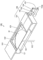
도 3은 노광 장치의 단면 사시도이다.
도 4는 노광 장치의 종단면도이다.
도 5는 케이스 내의 산소 농도와 배기 시간과의 관계를 나타내는 그래프이다.
도 6은 광원부에 의해 기판에 조사되는 진공 자외선의 조도와 광원부의 점등 시간의 관계를 나타내는 그래프이다.
도 7은 도 1의 제어부의 구성을 나타내는 기능 블럭도이다.
도 8은 노광 장치의 동작을 설명하기 위한 모식도이다.
도 9는 노광 장치의 동작을 설명하기 위한 모식도이다.
도 10은 노광 장치의 동작을 설명하기 위한 모식도이다.
도 11은 노광 장치의 동작을 설명하기 위한 모식도이다.
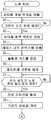
도 12는 도 7의 제어부에 의해 실시되는 노광 처리의 일례를 나타내는 플로차트이다.
도 13은 도 7의 제어부에 의해 실시되는 노광 처리의 일례를 나타내는 플로차트이다.
도 14는 도 7의 제어부에 의해 실시되는 노광 처리의 일례를 나타내는 플로차트이다.
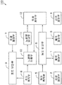
도 15는 도 1의 노광 장치를 구비한 기판 처리 장치의 전체 구성을 나타내는 모식적 블럭도이다.
도 16은 도 15의 기판 처리 장치에 의한 기판의 처리의 일례를 나타내는 모식도이다.
도 17은 본 발명의 제2 실시형태에 있어서의 노광 장치의 단면 사시도이다.
도 18은 도 17의 노광 장치의 종단면도이다.
도 19는 본 발명의 제3 실시형태에 있어서의 노광 장치의 단면 사시도이다.
도 20은 도 19의 노광 장치의 종단면도이다.
Claims (14)
- 기판의 피처리면에 진공 자외선을 조사 가능하게 설치된 투광부와,
상기 투광부로부터 기판에 진공 자외선을 조사하여 기판을 처리하는 조사 기간에, 진공 자외선의 일부를 수광하는 수광면을 가지고, 수광한 진공 자외선의 조도를 계측하는 조도계와,
상기 조사 기간에 있어서 기판의 처리 중에, 상기 조도계의 상기 수광면에의 진공 자외선의 입사를 단속적으로 차단하는 차광부와,
진공 자외선을 기판에 조사하도록 상기 투광부를 제어하는 것과 함께, 상기 조도계에 의해 계측된 조도에 의거하여 기판에의 진공 자외선의 조사를 정지하도록 상기 투광부를 제어하는 투광 제어부를 구비하는, 노광 장치. - 청구항 1에 있어서,
상기 조도계는, 상기 조사 기간에 있어서 상기 투광부로부터의 진공 자외선의 일부를 수광 가능한 위치에 설치되고,
상기 차광부는,
상기 조사 기간에 있어서 상기 조도계의 상기 수광면에의 진공 자외선의 입사를 단속적으로 차단하도록 이동 가능한 차광 부재와,
상기 차광 부재를 이동시키는 제1 구동부를 포함하는, 노광 장치. - 청구항 1에 있어서,
상기 차광부는, 상기 조도계를 상기 조사 기간에 있어서 상기 투광부로부터의 진공 자외선의 일부를 수광 가능한 제1 위치와 상기 투광부로부터의 진공 자외선을 수광 불가능한 제2 위치로 교대로 이동시키는 제2 구동부를 포함하는, 노광 장치. - 청구항 1 내지 청구항 3 중 어느 한 항에 있어서,
상기 투광부는, 기판의 일면의 전체 영역 및 기판 밖의 영역에 진공 자외선을 조사하도록 구성되고,
상기 조도계는, 상기 조사 기간에 있어서 상기 수광면에의 진공 자외선의 적어도 입사 시에 상기 기판 밖의 영역에 위치하는, 노광 장치. - 청구항 4에 있어서,
기판은 원형상을 가지고,
상기 투광부에 있어서의 진공 자외선의 출사부는, 기판의 상기 전체 영역에 상당하는 원형 영역을 내포하는 직사각형 형상을 가지며,
상기 조도계의 상기 수광면은, 상기 조사 기간에 있어서 상기 투광부의 상기 출사부에 있어서의 상기 원형 영역을 제외한 모서리부 영역으로부터 출사되는 진공 자외선이 입사 가능한 위치로 이동 가능하게 또는 고정적으로 배치되는, 노광 장치. - 청구항 1 내지 청구항 3 중 어느 한 항에 있어서,
상기 조도계는, 상기 수광면이 상기 조사 기간에 있어서의 기판의 피처리면을 기준으로 하는 일정한 높이에 위치하도록 배치되는, 노광 장치. - 청구항 6에 있어서,
상기 조도계는, 상기 수광면이 상기 조사 기간에 있어서의 기판의 피처리면과 동일한 높이에 위치하도록 배치되는, 노광 장치. - 청구항 1 내지 청구항 3 중 어느 한 항에 있어서,
처리 대상의 기판을 수용하는 처리실과,
상기 처리실 내에 있어서, 상기 투광부의 하방에 설치되며, 기판이 재치(載置)되는 재치부와,
상기 처리실 내와 외부 사이에서의 기판의 수도(受渡) 시에 상기 재치부가 제3 위치로 이동하고, 상기 투광부의 진공 자외선의 출사 시에 상기 재치부가 상기 제3 위치의 상방의 제4 위치로 이동하도록 상기 재치부를 제어하는 재치 제어부를 더 구비하는, 노광 장치. - 청구항 8에 있어서,
상기 조도계는, 상기 재치부의 이동에 추종하여 상하 방향으로 이동하는, 노광 장치. - 청구항 9에 있어서,
상기 재치부는,
기판이 재치되는 제1 부분과,
진공 자외선의 수광 시에 상기 조도계가 배치되는 제2 부분을 포함하는, 노광 장치. - 기판에 처리액을 도포함으로써 기판에 막을 형성하는 도포 처리부와,
상기 도포 처리부에 의해 막이 형성된 기판을 열처리하는 열처리부와,
상기 열처리부에 의해 열처리된 기판을 노광하는 청구항 1 내지 청구항 3 중 어느 한 항에 기재된 노광 장치와,
상기 노광 장치에 의해 노광된 기판에 용제를 공급함으로써 기판의 막을 현상 하는 현상 처리부를 구비하는, 기판 처리 장치. - 청구항 11에 있어서,
처리액은, 유도 자기 조직화 재료를 포함하는, 기판 처리 장치. - 투광부에 의해 기판의 피처리면에 진공 자외선을 조사하는 단계와,
상기 투광부로부터 기판에 진공 자외선을 조사하여 기판을 처리하는 조사 기간에, 조도계에 의해 진공 자외선의 일부를 수광하고, 수광한 진공 자외선의 조도를 계측하는 단계와,
상기 조사 기간에 있어서 기판의 처리 중에, 상기 조도계의 수광면에의 진공 자외선의 입사를 차광부에 의해 단속적으로 차단하는 단계와,
상기 조도계에 의해 계측된 조도에 의거하여 상기 투광부에 의한 기판에의 진공 자외선의 조사를 정지하는 단계를 포함하는, 노광 방법. - 도포 처리부에 의해 기판의 피처리면에 처리액을 도포함으로써 기판에 막을 형성하는 단계와,
상기 도포 처리부에 의해 막이 형성된 기판을 열처리부에 의해 열처리하는 단계와,
상기 열처리부에 의해 열처리된 기판을 노광 장치에 의해 노광하는 청구항 13에 기재된 노광 방법과,
상기 노광 장치에 의해 노광된 기판의 피처리면에 현상 처리부에 의해 용제를 공급함으로써 기판의 막을 현상하는 단계를 포함하는, 기판 처리 방법.
Applications Claiming Priority (3)
| Application Number | Priority Date | Filing Date | Title |
|---|---|---|---|
| JP2017038236A JP6768561B2 (ja) | 2017-03-01 | 2017-03-01 | 露光装置、基板処理装置、基板の露光方法および基板処理方法 |
| JPJP-P-2017-038236 | 2017-03-01 | ||
| PCT/JP2017/036074 WO2018159005A1 (ja) | 2017-03-01 | 2017-10-04 | 露光装置、基板処理装置、基板の露光方法および基板処理方法 |
Publications (2)
| Publication Number | Publication Date |
|---|---|
| KR20190102289A KR20190102289A (ko) | 2019-09-03 |
| KR102307596B1 true KR102307596B1 (ko) | 2021-09-30 |
Family
ID=63370897
Family Applications (1)
| Application Number | Title | Priority Date | Filing Date |
|---|---|---|---|
| KR1020197023927A KR102307596B1 (ko) | 2017-03-01 | 2017-10-04 | 노광 장치, 기판 처리 장치, 기판의 노광 방법 및 기판 처리 방법 |
Country Status (5)
| Country | Link |
|---|---|
| JP (1) | JP6768561B2 (ko) |
| KR (1) | KR102307596B1 (ko) |
| CN (1) | CN110100301B (ko) |
| TW (1) | TWI649642B (ko) |
| WO (1) | WO2018159005A1 (ko) |
Families Citing this family (2)
| Publication number | Priority date | Publication date | Assignee | Title |
|---|---|---|---|---|
| US11968772B2 (en) * | 2019-05-30 | 2024-04-23 | Kla Corporation | Optical etendue matching methods for extreme ultraviolet metrology |
| TWI747490B (zh) * | 2019-09-19 | 2021-11-21 | 日商斯庫林集團股份有限公司 | 曝光裝置 |
Citations (2)
| Publication number | Priority date | Publication date | Assignee | Title |
|---|---|---|---|---|
| JP2000100685A (ja) * | 1998-09-17 | 2000-04-07 | Nikon Corp | 露光装置及び該装置を用いた露光方法 |
| JP2006049730A (ja) | 2004-08-06 | 2006-02-16 | Sharp Corp | 露光装置、露光量制御方法、露光量制御プログラムとその記録媒体 |
Family Cites Families (14)
| Publication number | Priority date | Publication date | Assignee | Title |
|---|---|---|---|---|
| JP3378271B2 (ja) * | 1992-06-11 | 2003-02-17 | 株式会社ニコン | 露光方法及び装置、並びに前記方法を使用するデバイス製造方法 |
| JPH10229038A (ja) * | 1997-02-14 | 1998-08-25 | Nikon Corp | 露光量制御方法 |
| JPH10284407A (ja) * | 1997-04-08 | 1998-10-23 | Nikon Corp | 露光装置及び露光装置を用いた半導体デバイスの製造方法 |
| KR100564437B1 (ko) * | 1997-07-25 | 2006-03-29 | 가부시키가이샤 니콘 | 투영 노광 장치, 투영 노광 방법, 광 세정 방법 및 반도체디바이스의 제조 방법 |
| JPH11251220A (ja) * | 1998-03-02 | 1999-09-17 | Nikon Corp | 露光装置及び露光方法 |
| JP2001110710A (ja) * | 1999-10-08 | 2001-04-20 | Nikon Corp | 露光装置、露光方法、および半導体デバイスの製造方法 |
| US6211942B1 (en) * | 2000-03-10 | 2001-04-03 | Howa Machinery Ltd. | Double-sided exposure system |
| US20080012511A1 (en) * | 2004-07-15 | 2008-01-17 | Nikon Corporation | Planar Motor Device, Stage Device, Exposure Device and Device Manufacturing Method |
| JP4491445B2 (ja) * | 2005-11-04 | 2010-06-30 | 株式会社オーク製作所 | 周辺露光装置およびその方法 |
| JP4859660B2 (ja) * | 2006-12-27 | 2012-01-25 | 東京応化工業株式会社 | 基板処置装置 |
| JP2013104934A (ja) * | 2011-11-11 | 2013-05-30 | Tokyo Electron Ltd | 露光装置及び露光方法 |
| JP6535197B2 (ja) * | 2014-04-28 | 2019-06-26 | 株式会社ブイ・テクノロジー | 露光装置及び露光方法 |
| JP6495707B2 (ja) * | 2015-03-25 | 2019-04-03 | 株式会社Screenホールディングス | 露光装置および基板処理装置 |
| JP6543064B2 (ja) * | 2015-03-25 | 2019-07-10 | 株式会社Screenホールディングス | 露光装置、基板処理装置、基板の露光方法および基板処理方法 |
-
2017
- 2017-03-01 JP JP2017038236A patent/JP6768561B2/ja active Active
- 2017-10-04 KR KR1020197023927A patent/KR102307596B1/ko active IP Right Grant
- 2017-10-04 WO PCT/JP2017/036074 patent/WO2018159005A1/ja active Application Filing
- 2017-10-04 CN CN201780077239.0A patent/CN110100301B/zh active Active
- 2017-10-18 TW TW106135708A patent/TWI649642B/zh active
Patent Citations (2)
| Publication number | Priority date | Publication date | Assignee | Title |
|---|---|---|---|---|
| JP2000100685A (ja) * | 1998-09-17 | 2000-04-07 | Nikon Corp | 露光装置及び該装置を用いた露光方法 |
| JP2006049730A (ja) | 2004-08-06 | 2006-02-16 | Sharp Corp | 露光装置、露光量制御方法、露光量制御プログラムとその記録媒体 |
Also Published As
| Publication number | Publication date |
|---|---|
| KR20190102289A (ko) | 2019-09-03 |
| JP6768561B2 (ja) | 2020-10-14 |
| TWI649642B (zh) | 2019-02-01 |
| TW201833670A (zh) | 2018-09-16 |
| JP2018147918A (ja) | 2018-09-20 |
| WO2018159005A1 (ja) | 2018-09-07 |
| CN110100301A (zh) | 2019-08-06 |
| CN110100301B (zh) | 2023-07-21 |
Similar Documents
| Publication | Publication Date | Title |
|---|---|---|
| KR102103632B1 (ko) | 노광 장치, 기판 처리 장치, 기판의 노광 방법 및 기판 처리 방법 | |
| KR102153174B1 (ko) | 노광 장치, 기판 처리 장치, 노광 방법 및 기판 처리 방법 | |
| KR101764534B1 (ko) | 노광 장치, 기판 처리 장치, 기판의 노광 방법 및 기판 처리 방법 | |
| KR101217290B1 (ko) | 주변 노광 장치 | |
| CN108535965B (zh) | 曝光装置、基板处理装置、曝光方法及基板处理方法 | |
| KR102307596B1 (ko) | 노광 장치, 기판 처리 장치, 기판의 노광 방법 및 기판 처리 방법 | |
| WO2018173344A1 (ja) | 露光装置、基板処理装置、基板の露光方法および基板処理方法 | |
| TWI666525B (zh) | 曝光裝置及基板處理裝置 | |
| TWI676868B (zh) | 曝光裝置、基板處理裝置、基板之曝光方法及基板處理方法 | |
| TWI682433B (zh) | 曝光裝置、基板處理裝置、基板曝光方法以及基板處理方法 | |
| JP6924661B2 (ja) | 露光装置、基板処理装置、露光方法および基板処理方法 | |
| JP7002262B2 (ja) | 露光装置、基板処理装置、露光方法および基板処理方法 | |
| KR20210033913A (ko) | 노광 장치 |
Legal Events
| Date | Code | Title | Description |
|---|---|---|---|
| A201 | Request for examination | ||
| AMND | Amendment | ||
| PA0105 | International application |
Patent event date: 20190814 Patent event code: PA01051R01D Comment text: International Patent Application |
|
| PA0201 | Request for examination | ||
| PG1501 | Laying open of application | ||
| E902 | Notification of reason for refusal | ||
| PE0902 | Notice of grounds for rejection |
Comment text: Notification of reason for refusal Patent event date: 20201105 Patent event code: PE09021S01D |
|
| AMND | Amendment | ||
| E601 | Decision to refuse application | ||
| PE0601 | Decision on rejection of patent |
Patent event date: 20210512 Comment text: Decision to Refuse Application Patent event code: PE06012S01D Patent event date: 20201105 Comment text: Notification of reason for refusal Patent event code: PE06011S01I |
|
| AMND | Amendment | ||
| PX0901 | Re-examination |
Patent event code: PX09011S01I Patent event date: 20210512 Comment text: Decision to Refuse Application Patent event code: PX09012R01I Patent event date: 20210104 Comment text: Amendment to Specification, etc. Patent event code: PX09012R01I Patent event date: 20190814 Comment text: Amendment to Specification, etc. |
|
| PX0701 | Decision of registration after re-examination |
Patent event date: 20210701 Comment text: Decision to Grant Registration Patent event code: PX07013S01D Patent event date: 20210611 Comment text: Amendment to Specification, etc. Patent event code: PX07012R01I Patent event date: 20210512 Comment text: Decision to Refuse Application Patent event code: PX07011S01I Patent event date: 20210104 Comment text: Amendment to Specification, etc. Patent event code: PX07012R01I Patent event date: 20190814 Comment text: Amendment to Specification, etc. Patent event code: PX07012R01I |
|
| X701 | Decision to grant (after re-examination) | ||
| GRNT | Written decision to grant | ||
| PR0701 | Registration of establishment |
Comment text: Registration of Establishment Patent event date: 20210927 Patent event code: PR07011E01D |
|
| PR1002 | Payment of registration fee |
Payment date: 20210927 End annual number: 3 Start annual number: 1 |
|
| PG1601 | Publication of registration | ||
| PR1001 | Payment of annual fee |
Payment date: 20240821 Start annual number: 4 End annual number: 4 |