WO2018147372A1 - 光学素子成形用型の製造方法 - Google Patents
光学素子成形用型の製造方法 Download PDFInfo
- Publication number
- WO2018147372A1 WO2018147372A1 PCT/JP2018/004400 JP2018004400W WO2018147372A1 WO 2018147372 A1 WO2018147372 A1 WO 2018147372A1 JP 2018004400 W JP2018004400 W JP 2018004400W WO 2018147372 A1 WO2018147372 A1 WO 2018147372A1
- Authority
- WO
- WIPO (PCT)
- Prior art keywords
- temperature
- molding
- mold
- optical element
- film
- Prior art date
- Legal status (The legal status is an assumption and is not a legal conclusion. Google has not performed a legal analysis and makes no representation as to the accuracy of the status listed.)
- Ceased
Links
Images



Classifications
-
- C—CHEMISTRY; METALLURGY
- C03—GLASS; MINERAL OR SLAG WOOL
- C03B—MANUFACTURE, SHAPING, OR SUPPLEMENTARY PROCESSES
- C03B11/00—Pressing molten glass or performed glass reheated to equivalent low viscosity without blowing
-
- C—CHEMISTRY; METALLURGY
- C03—GLASS; MINERAL OR SLAG WOOL
- C03B—MANUFACTURE, SHAPING, OR SUPPLEMENTARY PROCESSES
- C03B40/00—Preventing adhesion between glass and glass or between glass and the means used to shape it, hold it or support it
- C03B40/02—Preventing adhesion between glass and glass or between glass and the means used to shape it, hold it or support it by lubrication; Use of materials as release or lubricating compositions
-
- C—CHEMISTRY; METALLURGY
- C23—COATING METALLIC MATERIAL; COATING MATERIAL WITH METALLIC MATERIAL; CHEMICAL SURFACE TREATMENT; DIFFUSION TREATMENT OF METALLIC MATERIAL; COATING BY VACUUM EVAPORATION, BY SPUTTERING, BY ION IMPLANTATION OR BY CHEMICAL VAPOUR DEPOSITION, IN GENERAL; INHIBITING CORROSION OF METALLIC MATERIAL OR INCRUSTATION IN GENERAL
- C23C—COATING METALLIC MATERIAL; COATING MATERIAL WITH METALLIC MATERIAL; SURFACE TREATMENT OF METALLIC MATERIAL BY DIFFUSION INTO THE SURFACE, BY CHEMICAL CONVERSION OR SUBSTITUTION; COATING BY VACUUM EVAPORATION, BY SPUTTERING, BY ION IMPLANTATION OR BY CHEMICAL VAPOUR DEPOSITION, IN GENERAL
- C23C14/00—Coating by vacuum evaporation, by sputtering or by ion implantation of the coating forming material
- C23C14/06—Coating by vacuum evaporation, by sputtering or by ion implantation of the coating forming material characterised by the coating material
- C23C14/14—Metallic material, boron or silicon
-
- G—PHYSICS
- G02—OPTICS
- G02B—OPTICAL ELEMENTS, SYSTEMS OR APPARATUS
- G02B3/00—Simple or compound lenses
Definitions
- the present invention relates to a method of manufacturing a mold for molding an optical element.
- Priority is claimed on Japanese Patent Application No. 2017-020866, filed Feb. 8, 2017, the content of which is incorporated herein by reference.
- Patent Document 1 describes a glass molding die protective film made of a nitrogen compound.
- the chemical structure of the nitrogen compound contains a hydrogen atom.
- Patent Document 2 describes a method of manufacturing an optical element molding die provided with a surface layer. The surface layer is formed mainly of a hard carbon film or a noble metal-based alloy film.
- the mold protection film for glass molding described in Patent Document 1 is made of a nitrogen compound containing hydrogen atoms in order to reduce the amount of oxygen in the protection film for mold for glass formation.
- the reason for this is that when the amount of oxygen is large, film peeling is likely to occur.
- the oxygen in the protective film for molding glass and the glass component react with each other, fusion of the glass component tends to occur due to the reaction product.
- the peeling of the film is apt to occur due to the fusion of the glass component.
- the hydrogen atom bonds to the metal atom in the nitrogen compound the melting point of the nitrogen compound is lowered.
- the heat resistance of the glass molding die protective film is lowered.
- the durability may be reduced in the glass molding die protective film described in Patent Document 1.
- the surface layer is formed mainly of a hard carbon film or a noble metal-based alloy film.
- the hard carbon film is heated to 600 ° C. or more, graphitization occurs.
- the hard carbon film turns into a brittle film.
- the mold for molding an optical element having a surface layer mainly composed of a hard carbon film has reduced durability at high temperatures of 600 ° C. or higher.
- the surface layer mainly composed of a noble metal-based alloy film is excellent in heat resistance.
- the surface layer mainly composed of a noble metal-based alloy film easily reacts with the glass component. For this reason, in the surface layer mainly composed of a noble metal-based alloy film, fusion tends to occur during repeated use. For this reason, the durability of the optical element molding die is poor.
- the present invention has been made in view of the above problems, and an object of the present invention is to provide a method of manufacturing a mold for forming an optical element having excellent durability even if molding at high temperature is repeated.
- an optical element molding die of the first aspect of the present invention preparing a substrate having a molding surface, and heating the substrate, Forming a release film on the molding surface while the base material is heated; And the molding surface has a shape for molding an optical element using a heated glass material, the mold release film has an outermost layer containing a noble metal element, and At the time of film formation of the surface layer, as a result of heating the base material, the temperature of the film formation surface is kept within a first temperature range, and the first temperature range shapes the optical element above the deformation point of the glass material Below the molding temperature.
- the mold release film includes an intermediate layer, and the intermediate layer is laminated on the molding surface
- the intermediate layer forms the film formation surface at the time of film formation of the outermost layer, and when the intermediate layer is formed, the temperature of the film formation surface is as a result of heating the substrate.
- a second temperature range may be maintained, and the second temperature range may be equal to or lower than a lower limit temperature of the first temperature range.
- the temperature of the molding surface is a lower limit in the second temperature range at the time of film formation of the intermediate layer.
- the temperature may be raised from the temperature to the upper limit temperature.
- the temperature of the film forming surface is set at the time of film formation of the outermost layer.
- the temperature may be raised from the lower limit temperature to the upper limit temperature in the first temperature range.
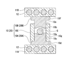
- FIG. 1 is a schematic vertical sectional view showing an example of an optical element molding die manufactured by the method of manufacturing an optical element molding die according to the first embodiment of the present invention.
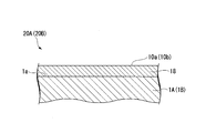
- FIG. 2 is a schematic cross-sectional view showing a configuration of a mold release film in an optical element molding die manufactured by the method of manufacturing an optical element molding die according to the first embodiment of the present invention.
- the optical element molding die is manufactured by the method of manufacturing the optical element molding die of the present embodiment.
- the molding die assembly 10 includes a lower die 10A (optical element molding die), an upper die 10B (optical element molding die), and a barrel die 10C.
- the central axes of the lower mold 10A, the upper mold 10B, and the barrel 10C are coaxial with each other.
- the mold assembly 10 is used to mold an optical element.
- the optical element is manufactured using a glass material.
- the type and shape of the optical element molded using the mold assembly 10 are not limited. For example, a lens, a mirror, a prism, a parallel plate, etc. are mentioned as an example of an optical element.
- the mold assembly 10 shown in FIG. 1 molds, for example, a flanged biconvex lens.
- the lower mold 10A is made of a substantially cylindrical member.
- the lower mold 10A includes a cylindrical side surface 10c.
- a mold surface 10a is formed at a first end in the axial direction (the upper end in the drawing in FIG. 1).
- the mold surface 10a transfers the surface shape of the optical element to the glass material.
- the shape of the mold surface 10a may be a combination of a concave surface forming the convex lens surface and a plane surface forming the flange surface.
- a flange portion 10d is formed at the second end of the lower mold 10A.
- the second end of the lower mold 10A is an end opposite to the first end in the axial direction.
- the flange portion 10d extends radially outward from the side surface 10c of the lower mold 10A.
- the mold surface 10 a is formed by the mold release film 8.
- the mold release film 8 is formed on the molding surface 1a.
- the molding surface 1a is formed on the base 1A.
- the substrate 1A is manufactured using a material having high heat resistance and high hardness.
- a material of the substrate 1A for example, a cemented carbide, silicon carbide, carbon or the like may be used.
- the main component of the cemented carbide is tungsten carbide (WC).
- the substrate 1A may constitute the entire lower mold 10A excluding the release film 8.
- the substrate 1A may be disposed only at the first end of the lower mold 10A.
- the molding surface 1a has a shape close to the surface of the optical element to be molded.
- the molding surface 1a is mirror-polished.
- the surface accuracy of the molding surface 1a may be 0.15 ⁇ m or less in PV value.
- the surface roughness of the molding surface 1a may be 3 nm or less in arithmetic average roughness Ra.
- the release film 8 includes an outermost layer 7 and an intermediate layer 6.
- the outermost layer 7 forms a mold surface 10a.
- the mid layer 6 is formed between the molding surface 1 a of the base 1 A and the outermost layer 7. As described later, the intermediate layer 6 and the outermost layer 7 are deposited on the molding surface 1a. The mid layer 6 and the outermost layer 7 are laminated in this order on the molding surface 1 a.
- the outermost layer 7 contains a noble metal element.
- the type of the noble metal element contained in the outermost layer 7 is not particularly limited.
- the outermost layer 7 is made of platinum (Pt), gold (Au), iridium (Ir), rhenium (Re), silver (Ag), osmium (Os), tantalum (Ta), and palladium (Pd). At least one or more elements selected from the group may be included.
- the noble metal element is less likely to cause a chemical reaction with the glass component of the glass material at the molding temperature of the glass material. For this reason, the releasability of the outermost layer 7 with respect to the formed glass material becomes good.
- the intermediate layer 6 is composed of a single layer film or a multilayer film.
- the intermediate layer 6 may include a graded layer.
- the inclined layer is a layer in which the composition ratio of each component changes in the layer thickness direction.
- the intermediate layer 6 may be configured to include the first component and the second component.
- the first component is a component having good adhesion to the base material 1A (1B).
- the second component is a component having good adhesion to the outermost layer 7.
- the intermediate layer 6 is a sloped layer, the composition ratio of the first component gradually increases from the molding surface 1a (1b) side to the surface 6a side, and the composition ratio of the second component is the molding surface 1a.
- the adhesion strength between the intermediate layer 6 and the molding surface 1a is improved. Furthermore, the adhesion strength between the surface 6 a of the intermediate layer 6 and the outermost layer 7 is improved.
- the material of the intermediate layer 6 a material having good adhesion to the material of the molding surface 1a and the material of the outermost layer 7 is used.
- the material of the intermediate layer 6 is appropriately selected according to the material of the molding surface 1 a of the base material 1A (1B) and the material of the outermost layer 7.
- examples of materials suitable for the intermediate layer 6 include titanium (Ti), tantalum (Ta), chromium (Cr), aluminum (Al), molybdenum (Mo) and the like.
- the mid layer 6 may contain part of the components of the base material 1A (1B).
- the mid layer 6 may contain part of the components of the outermost layer 7.
- the intermediate layer 6 is deposited prior to the outermost layer 7. Therefore, the surface 6 a of the intermediate layer 6 is a film formation surface at the time of film formation of the outermost layer 7.
- Upper mold 10B consists of a substantially cylindrical member.
- the upper mold 10B is provided with a cylindrical side surface 10e.
- a mold surface 10b is formed at a first end in the axial direction (the lower end in the drawing in FIG. 1).
- the mold surface 10 b transfers the surface shape of the optical element to the glass material.
- the shape of the mold surface 10b may be a combination of a concave surface forming the convex lens surface and a plane surface forming the flange surface.
- a flange portion 10f is formed at the second end of the upper mold 10B.
- the second end of the upper mold 10B is an end opposite to the first end in the axial direction.
- the flange portion 10 f extends radially outward from the side surface 10 e of the upper mold 10 B.
- the mold surface 10 b is formed of a release film 8 similar to the mold surface 10 a.
- the mold release film 8 on the mold surface 10 b is formed on the molding surface 1 b.
- the molding surface 1b is formed on the base 1B.
- the substrate 1B is manufactured using the same material as the substrate 1A. Similar to the substrate 1A, the substrate 1B may constitute the entire upper mold 10B excluding the release film 8. The substrate 1B may be disposed only at the first end of the upper mold 10B.
- the molding surface 1 b has a shape close to the surface of the optical element to be molded.
- the molding surface 1b is mirror-polished. The surface precision and surface roughness of the molding surface 1b are the same as those of the molding surface 1a.
- the body mold 10C is a cylindrical member.
- the body mold 10C has an inner circumferential surface 10g.
- the inner circumferential surface 10g slidably engages the side surface 10c of the lower mold 10A and the side surface 10e of the upper mold 10B.
- the length of the cylinder mold 10C in the axial direction of the cylinder mold 10C is shorter than the distance between the flanges 10d and 10f in the assembled state of the molding mold assembly 10 described later.
- the body mold 10C can hold the lower mold 10A and the upper mold 10B in a coaxial positional relationship while molding is performed.
- the body mold 10C can guide the upper mold 10B movably in the axial direction.
- the body mold 10C is made of an appropriate material having heat resistance to the molding temperature.
- a metal material or a ceramic may be used as the material of the body mold 10C.
- a cemented carbide is used as an example of the body mold 10C.
- a cemented carbide is a material having high hardness and good heat resistance.
- the first ends of the lower mold 10A and the upper mold 10B are inserted into the barrel mold 10C.
- a molding material G is disposed between the mold surfaces 10a, 10b. The molding material G is weighed to a mass necessary for molding.
- the molding material G is made of an appropriate glass material for forming an optical element.
- the molding material G is molded into an appropriate massive shape.
- the shape of the molding material G is not particularly limited as long as it is a shape that can be press-molded by the molding die assembly 10.
- the shape of the molding material G is spherical.
- the shape of the molding material G may be, for example, a disk shape, a spheroid shape, a similar shape of an optical element, or the like.
- the means for molding the molding material G is not particularly limited.
- the molding material G may be molded.
- the molding material G may be molded by machining such as cutting and polishing.
- FIG. 3 is process explanatory drawing of the manufacturing method of the type
- the difference between the lower mold 10A and the upper mold 10B is only the shape of the molding surfaces 1a and 1b. So, below, the manufacturing method of the type
- a substrate 1A is prepared.
- the molding surface 1a is formed on the base material 1A as follows.
- the outer shape of the optical element is identified.
- the molding material G used for molding is specified.
- the molding material G is molded into the shape of the optical element at the molding temperature T mo .
- the molding temperature T mo is higher than the deformation point T at of the molding material G.
- a material used for the substrate 1A a material that withstands the molding temperature T mo is selected.
- the material used for the base material 1A is formed in a shape such as a shape in which the flange portion 10d protrudes from an end of a cylinder having the side surface 10c. Thereafter, the molding surface 1a is formed at the end of the cylinder opposite to the flange portion 10d. In the finishing process of the molding surface 1a, mirror polishing is performed. Above, base material 1A which has molding side 1a is prepared.
- the mold release film 8 is formed on the molding surface 1a.
- the mold release film 8 is formed on the molding surface 1a.
- the substrate 1 ⁇ / b> A is in a heated state.
- the film forming method for example, vapor deposition, RF sputtering, DC sputtering, magnetron sputtering, ion beam sputtering, ion plating, ion mixing and the like can be mentioned.
- the release film 8 is formed by DC sputtering will be described.
- the film forming apparatus 100 shown in FIG. 3 forms the intermediate layer 6 and the outermost layer 7 using DC sputtering.
- the film forming apparatus 100 has a vacuum chamber 101.
- the vacuum chamber 101 includes an exhaust port, a vacuum pump, an intake port, and a gas supply unit.
- the exhaust port is used for evacuation at the time of evacuation.
- the vacuum pump is connected to the exhaust port.
- the inlet is used to supply gas.
- the gas supply unit is connected to the intake port.
- the gas supply unit supplies an inert gas to the inside of the vacuum chamber 101.
- An inert gas is supplied to form an inert atmosphere. Examples of inert gases include, for example, argon (Ar) gas.
- sample stages 106 and 107 and a heating dome 102 are disposed.
- the sample tables 106 and 107 are provided with electrodes (not shown).
- An electrode (not shown) is connected to the negative electrode of the DC power supply.
- the sample tables 106 and 107 are spaced apart from each other.
- a partition plate 108 is disposed between the sample tables 106 and 107.
- the divider 108 prevents mixing of the sputtered material.
- the target 104 is disposed on the sample table 106.
- the target 104 is formed of a material that forms the intermediate layer 6.
- the target 105 is disposed on the sample table 107.
- the target 105 is formed of a material that forms the outermost layer 7.
- FIG. 3 is a schematic view, one target 104 and one target 105 are drawn.
- the target 104 (105) may be composed of a plurality of members.
- the materials of the plurality of members may be different from each other.
- the plurality of members may be disposed on different electrodes.
- the heating dome 102 holds the film formation target in a state of being directed to the lower side of the film formation surface of the film formation target.
- the heating dome 102 is provided with a heater 103.
- the heater 103 heats the held film formation target.
- the heating dome 102 is disposed above the sample pedestals 106 and 107.
- the heating dome 102 is movably supported by a moving mechanism (not shown).
- the heating temperature of the heater 103 is controlled so that the temperature of the film formation surface of the film formation object at the time of film formation becomes a preset time function.
- the heater 103 include, for example, a lamp heater, a sheath heater, and a cartridge heater.
- a carbon lamp heater may be used as the heater 103.
- the lamp heater made of carbon can heat at a high temperature of about 1000 ° C., for example.
- the positive electrode voltage of the DC power supply is applied to the film formation target held by the heating dome 102.
- the film forming process of the release film 8 is divided into an outermost layer film forming process for forming the intermediate layer 6 and an intermediate layer film forming process for forming the outermost layer 7.
- the intermediate layer 6 is formed.
- the outermost layer 7 is formed.
- the outermost layer film forming process and the intermediate layer film forming process are performed in this order in the film forming apparatus 100.
- the heater 103 of the film forming apparatus 100 is temperature controlled during the intermediate layer film forming process.
- the heater 103 keeps the temperature of the molding surface 1a in the second temperature range during the intermediate layer film forming process.
- the forming surface 1 a is a film forming surface on which the intermediate layer 6 is formed.
- the temperature of the heater 103 is controlled during the outermost layer deposition process.
- the heater 103 keeps the temperature of the surface 6 a in the first temperature range during the outermost layer film forming process.
- the surface 6 a is a film formation surface on which the outermost layer 7 is formed.
- the first temperature range is a temperature range selected from the range between the deformation point T at of the molding material G and the molding temperature T mo .
- the lower limit temperature and the upper limit temperature may be the same.
- the temperature of the surface 6a may change with time as long as it is in the range of the first temperature range. For example, the temperature of the surface 6a may fluctuate from the average temperature while the outermost layer film forming process is performed.
- the temperature of the surface 6a may be monotonously increased in a broad sense from the lower limit temperature to the upper limit temperature while the outermost layer film forming step is performed.
- “broadly monotonically increasing” means increasing non-decreasing from the lower limit value to the upper limit value.
- the second temperature range is a temperature range equal to or lower than the lower limit temperature of the first temperature range.
- the lower limit temperature of the second temperature range may be 30% or more of the lower limit temperature of the first temperature range.
- the lower limit temperature of the second temperature range is more preferably 50% or more of the lower limit temperature of the first temperature range.
- the temperature of the molding surface 1a may change with time as long as it is in the second temperature range.
- the temperature of the molding surface 1a may fluctuate from the average temperature while the intermediate layer film forming process is performed.
- the temperature of the molding surface 1a may be monotonously increased in a broad sense from the lower limit temperature to the upper limit temperature while the intermediate layer film forming step is performed.
- the second temperature range may have the same lower limit temperature and upper limit temperature.
- FIG. 4 shows a setting example of temperature change in the second temperature range and the first temperature range in the present embodiment.
- FIG. 4 is a schematic graph showing an example of the temperature change of the film forming surface in the method of manufacturing an optical element molding die according to the first embodiment of the present invention.
- the horizontal axis of the graph of FIG. 4 represents time, and the vertical axis represents the temperature of the film formation surface.
- the film forming surface means the molding surface 1 a until the intermediate layer film forming process is completed.
- the film forming surface means the surface 6 a from the end of the intermediate layer film forming step to the end of the outermost layer film forming step.
- n of t n (where n is a natural number) described on the horizontal axis represents the magnitude relation in the horizontal axis. For example, when i ⁇ j, t i ⁇ t j (the same applies to the graphs in FIGS. 5 and 7 below).
- temperatures T 1 may include a minute fluctuation generated on the temperature control of the heater 103.
- temperatures T 1 may vary within a range of ⁇ [Delta] T 1 to the control target value T 1.
- the temperature width ⁇ T 1 may be 0 ° C. or more and 50 ° C. or less.
- the temperatures T 1 - ⁇ T 1 and T 1 + ⁇ T 1 are respectively the lower limit temperature and the upper limit temperature of the second temperature range.
- the time t 2 is set to a value at which sputtering for forming the intermediate layer 6 can be performed during a time t 2 -t 1 .
- the temperature of the deposition surface is heated toward the temperatures T 1 to the temperature T 2.
- the temperature of the deposition surface is maintained at a constant temperature T 2.
- temperature T 2 may comprise a slight change that occurs on the temperature control of the heater 103.
- temperature T 2 may vary within a range of ⁇ [Delta] T 2 relative to the control target value T 2.
- the temperature width ⁇ T 2 may be 0 ° C. or more and 40 ° C. or less.
- the temperatures T 2 ⁇ T 2 and T 2 + ⁇ T 2 are the lower limit temperature and the upper limit temperature of the first temperature range, respectively.
- Time t 4 during the time t 4 -t 3, the sputtering for forming the outermost layer 7 is set to executable value. After time t 4, the temperature of the deposition surface is lowered.
- the base material 1A is attached to the heating dome 102.
- the substrate 1A is a film formation target.
- the substrate 1A is fixed in a posture in which the molding surface 1a faces downward.
- Targets 104 and 105 are disposed on the electrodes of the sample tables 106 and 107, respectively.
- the heating dome 102 is moved above the target 104 by a moving mechanism (not shown). As a result, the molding surface 1 a is disposed at a position facing the target 104. Thereafter, evacuation is performed from the vacuum chamber 101. Ar gas is introduced into the vacuum chamber 101. Thereafter, the heating of the heater 103 based on the broken line 200 shown in FIG. 4 is started.
- the intermediate layer film forming process is started.
- a DC voltage is applied between the electrode of the heating dome 102 and the electrode of the sample stage 106.
- a substrate 1A is disposed on the electrode of the heating dome 102.
- a plasma is generated between the molding surface 1 a and the target 104 by the application of the DC voltage.
- the target 104 is sputtered by the plasma. Sputtered particles fly out of the target 104 by sputtering. Sputtered sputtered particles adhere to the molding surface 1a. As described above, while the DC sputtering is continued, sputtered particles are deposited on the molding surface 1a.
- the intermediate layer 6 is formed by the sputtered particles.
- a partition plate 108 is provided between the targets 104 and 105. For this reason, sputtered particles generated from the target 104 do not adhere to the target 105. Furthermore, no plasma is generated between the target 105 and the molding surface 1a. Therefore, the target 105 is not sputtered.
- the voltage application is stopped. Thus, the intermediate layer film forming process in the film forming process is completed.
- Intermediate layer forming step may be performed in any time zone from the time t 1 to time t 2.
- the intermediate layer forming step while the molding surface 1a is kept at a temperature T 1, the intermediate layer 6 is laminated onto the molding surface 1a.
- the forming surface 1a is a film forming surface in the intermediate layer film forming step.
- Atsushi Nobori of the film-forming surface by the heating of the heater 103 is started.
- the outermost layer deposition process is started.
- the heating dome 102 by not shown moving mechanism is moved above the target 105.
- the heating dome 102 may be moved above the target 105 during the time t 2 to time t 3.
- the surface 6a of the intermediate layer 6 is disposed at a position facing the target 105, as indicated by a two-dot chain line in FIG.
- the outermost layer film forming process is started.
- a DC voltage is applied between the electrode of the heating dome 102 and the electrode of the sample stage 107.
- a substrate 1A is disposed on the electrode of the heating dome 102.
- a plasma is generated between the surface 6 a and the target 105 by application of a DC voltage.
- the target 105 is sputtered by the plasma. Sputtered particles fly out of the target 105 by sputtering. Sputtered sputtered particles adhere to the surface 6a.
- DC sputtering is continued, sputtered particles are deposited on the surface 6a.
- the outermost layer 7 is formed by the sputtered particles.
- a partition plate 108 is provided between the targets 104 and 105. Therefore, sputtered particles generated from the target 105 do not adhere to the target 104. Furthermore, no plasma is generated between the target 104 and the surface 6a. Therefore, the target 104 is not sputtered.
- DC sputtering by the target 105 is performed until the layer thickness of the outermost layer 7 reaches a target, voltage application is stopped. Above, the outermost layer film-forming process in a film-forming process is complete
- the outermost layer deposition process while the surface 6a is kept at a temperature T 2, the outermost layer 7 is laminated on the surface 6a.
- the surface 6a is a film forming surface in the outermost layer film forming step.
- the heating of the heater 103 is stopped.
- the temperature of the substrate 1A decreases to a temperature at which it can be removed from the vacuum chamber 101, the reduced pressure of the vacuum chamber 101 is released.
- the substrate 1A is taken out of the vacuum chamber 101 to the outside.
- the lower mold 10A on which the mold release film 8 is formed is manufactured.
- the release film 8 can be formed on the molding surface 1b of the base material 1B by the film forming apparatus 100 in the same manner as described above. Thus, the upper mold 10B is manufactured.
- the forming of the optical element using the lower mold 10A and the upper mold 10B is performed as follows. As shown in FIG. 1, the mold assembly 10 is assembled. A molding material G is disposed inside the molding die assembly 10. Thereafter, the mold assembly 10 is held by the heating plates 11A and 11B. The heating plates 11A and 11B are disposed in the dustproof processing chamber. The heating plate 11A supports the flange portion 10d of the lower mold 10A from below. The heating plate 11B is in contact with the flange portion 10f of the upper mold 10B from above. The heating plate 11B can press the upper mold 10B toward the lower mold 10A by a pressing mechanism (not shown). Heaters 12 are respectively disposed inside the heating plates 11A and 11B.
- a ceramic cartridge heater may be used as the heater 12.
- the heater 12 heats the heating plates 11A and 11B.
- the heater 12 heats the lower mold 10A and the upper mold 10B by heat conduction from the heating plates 11A and 11B.
- the heater 12 continues heating until the temperature of the mold surfaces 10a and 10b of the lower mold 10A and the upper mold 10B reaches the molding temperature T mo .
- the heater 12 keeps the temperature of the mold surfaces 10a and 10b at the molding temperature T mo until the molding is completed.
- the molding temperature T mo is set to a temperature at which the molding material G is in a softened state that is easily deformed.
- the molding temperature T mo is set to, for example, a temperature equal to or higher than the deformation point T at .
- the molding material G is heated by the radiation from the mold surfaces 10a and 10b and the heat conduction from the contact portion of the mold surfaces 10a and 10b.
- the heating plate 11B is lowered by a pressing mechanism (not shown).
- the pressure in the press mechanism may be, for example, 0.3 MPa.
- the heating plate 11B is lowered, the molding material G between the lower mold 10A and the upper mold 10B is press-formed.
- each outermost layer 7 comes into contact with the molding material G while being heated to the molding temperature T mo .
- Each outermost layer 7 forms mold surfaces 10a and 10b, respectively.
- the pressing mechanism is stopped.
- the heating of the heating plates 11A and 11B is stopped.
- the radiation cooling of the molding die assembly 10 is started.
- the shape of the mold surfaces 10 a and 10 b is transferred to the molding material G in the mold assembly 10.
- a press-formed molded article is formed.
- the cooling plate for cooling the molding die assembly 10 is provided in the molding chamber, the molding die assembly 10 is moved to the cooling plate after the holding of the heating plates 11A and 11B is released. .
- the cooling plate cools the mold assembly 10.
- the molded article is demolded from the mold assembly 10. In this way, a molded article having the outer shape of the optical element is manufactured.
- the molded product is subjected to machining such as centering or an appropriate film coating, as necessary. Thus, the optical element is manufactured.
- the lower mold 10A (upper mold 10B) is heated from normal temperature before the start of use to the molding temperature T mo and cooled from the molding temperature T mo to the normal temperature.
- each part of the lower mold 10A repeats expansion and contraction in accordance with the respective thermal expansion coefficients.
- the substrate 1A (1B) and the intermediate layer 6 have different coefficients of thermal expansion.
- the intermediate layer 6 and the outermost layer 7 have different coefficients of thermal expansion. Therefore, thermal stress is generated at the respective interfaces during expansion and contraction.
- stress due to pressure from the press mechanism is also generated in the lower mold 10A (upper mold 10B). For this reason, the thermal stress generated at the time of press molding has a particularly great influence on the durability of the intermediate layer 6 and the outermost layer 7.
- the surface 6a of the intermediate layer 6 is heated to a temperature T 2. Therefore, in a state of being heated to a temperature T 2, the thermal stress generated at the interface between the intermediate layer 6 and the outermost layer 7 is minimized. Temperature T 2 is close to the far forming temperature T mo compared to normal temperature, the thermal stress in the state of being heated to the molding temperature T mo is significantly reduced. For this reason, the stress load between the middle layer 6 and the outermost layer 7 generated at the time of press forming is reduced. As a result, peeling between the outermost layer 7 and the intermediate layer 6 is suppressed. As a result, the durability of the outermost layer 7 is improved.
- the intermediate layer 6 when forming the intermediate layer 6, the molding surface 1a of the substrate 1A (1B) is heated to a temperature T 1. Therefore, in a state of being heated to a temperature T 1, the thermal stress generated at the interface between the substrate 1A (1B) and the intermediate layer 6 is minimized. Temperature T 1 is lower than the temperature T 2. Therefore, the intermediate layer 6 has a function of alleviating strain between the molding surface 1a and the lower surface of the outermost layer 7 in the process of raising and lowering the lower mold 10A (upper mold 10B) between the normal temperature and the molding temperature.
- the intermediate layer 6 is formed of the inclined layer in which the composition of the first component is large on the molding surface 1a (1b) side and the composition of the second component is large on the surface 6a
- the adhesion strength between the intermediate layer 6 and the base material 1A (1B) and the outermost layer 7 becomes better. For this reason, peeling of the release film 8 is further less likely to occur.
- the thermal stress acting on each part by the heat cycle is reduced. For this reason, the occurrence of fusion of the molding material G is suppressed.
- the fusion of the glass occurs due to the deterioration of the mold release performance of the mold release film 8 with time.
- the inventor conducted a component analysis of the release film in which glass fusion occurred. As a result of the component analysis, it was revealed that the glass component penetrates into the interstices of the grain boundaries in the release film at the fusion-bonded portion of the glass. The glass component that has penetrated into the interstices of such crystal grain boundaries has high affinity with the glass on the surface of the release film. For this reason, it is easy to combine a glass component.
- the bonded glass component is strongly bonded to the glass component in the grain boundaries. This causes fusion with the surface of the molded article. If the molded product is forcibly demolded in this state, a part of the glass on the surface of the molded product is taken to the parting film side. For this reason, a crack etc. generate
- the gap of the grain boundary caused by the expansion due to the thermal expansion of the outermost layer 7 is suppressed.
- the gap between the crystal grain boundaries becomes small also at the point where the outermost layer 7 becomes close to the state of being densely deposited by sputtering.
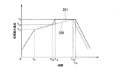
- FIG. 5 is a schematic graph showing an example of the temperature change of the film forming surface in the method of manufacturing the mold for molding an optical element according to a modification (first modification, second modification) of the first embodiment of the present invention. It is.
- the horizontal axis of the graph of FIG. 5 represents time, and the vertical axis represents the temperature of the film formation surface.
- the method of manufacturing a mold for forming an optical element according to the present modification is a method of manufacturing the lower mold 10A (upper mold 10B) by forming the mold release film 8 on the molding surface 1a (1b) of the base 1A (1B). It is.
- the configuration of the substrate 1A (1B) is the same as that of the first embodiment.
- the temperature of the film forming surface in the intermediate layer film forming step is monotonously increased in a broad range in the second temperature range.
- the broken line 201 in FIG. 5 shows a setting example of the temperature change in the second temperature range and the first temperature range in the present modification.
- the temperature of the deposition surface when heated by the heater 103 is started, the temperature of the deposition surface to a temperature T 11 at the time t 11. From the time t 11 to time t 12, the temperature of the deposition surface temperature T 12 (although, T 12> T 11) from the temperature T 11 is weakly monotonically increases to.
- the time t 11 is the time at which the intermediate layer forming step is started.
- Time t 12 is the time at which the intermediate layer forming step is completed.
- the broken line 201 in FIG. 5 illustrates an example in which the temperature of the film formation surface linearly increases with time.
- the temperature of the deposition surface a portion between the time t 11 to time t 12, the portion to remain constant may be provided.
- the temporally changing portion of the temperature of the film formation surface may increase in a narrowly monotonous manner in a curved or broken line shape.
- “in a narrow sense monotonous increase” is a change such that T (t i ) ⁇ T (t j ) if t i ⁇ t j when the temperature T is represented by a time function like T (t).
- the temperatures T 11 and T 12 appropriate values that satisfy the conditions of the second temperature range described above are used.
- the temperature T 11 can be equal to temperature T 1 of in the first embodiment.
- Temperature T 11 is greater than the maximum value of the temperatures T 1 in the first embodiment, it may be less than the minimum value of the temperature T 2.
- the temperature of the deposition surface is heated toward the same temperature T 2 in the first embodiment from the temperature T 12. From the time t 13 to time t 15, the temperature of the deposition surface is maintained at a constant temperature T 2 at the first temperature range.
- the time t 13 is the time at which the outermost layer film formation process is started.
- Time t 15 is the time at which the outermost layer deposition process is terminated. After time t 15, the temperature of the deposition surface is lowered.
- the second temperature range is equal to or higher than the temperature T 11 (lower limit temperature) and equal to or lower than the temperature T 12 (upper limit temperature).
- the first temperature range is a temperature T 2 ⁇ T 2 (lower limit temperature) or more and a temperature T 2 + ⁇ T 2 (upper limit temperature) or less.
- a T 12 ⁇ T 2 - ⁇ T 2 is a temperature T 12 ⁇ T 2 - ⁇ T 2.
- the intermediate layer forming step from the time t 11 to time t 12 the temperature of the molding surface 1a is the film-forming surface is weakly monotonically increases from the temperature T 11 to a temperature T 12 Be done.
- the temperature of the surface 6a is similar to the first embodiment is kept at a temperature T 2.
- the surface 6a is a film forming surface in the outermost layer film forming step in the present modification.
- the temperature of the film formation surface monotonously increases in a broad sense when the temperature of the film formation surface is raised.
- the temperature of the portion of the intermediate layer 6 already formed on the molding surface 1a is also raised.
- the film forming material is deposited on the surface of the intermediate layer 6 which has been formed into a film in a state of being thermally expanded according to the temperature during the temperature rise. Therefore, distortion due to thermal expansion in the surface 6a of the intermediate layer 6 is minimized at a temperature T 12.
- such an intermediate layer 6 has a gradually increasing residual strain in the layer thickness direction from the molding surface 1a to the surface 6a.
- the outermost layer 7 has a residual strain greater than that of the middle layer 6 in a normal temperature environment.
- the temperature of the mold surface 10a (10b) rises to the molding temperature T mo .
- the residual strain of the intermediate layer 6 and the outermost layer 7 at normal temperature is released.
- T 12 strain the intermediate layer 6 is gradually begin to increase.
- the residual strain of the outermost layer 7 formed on the surface 6 a is further released. Residual strain of the outermost layer 7 is minimized at a temperature T 2. Therefore, at the time of press molding, the thermal expansion of the outermost layer 7 depends on the temperature difference T mo -T 2 as in the first embodiment.
- the thermal expansion of the surface 6a in the intermediate layer 6 depends on the temperature difference T mo -T 12 ( ⁇ T mo -T 1 ). Therefore, the thermal stress at the interface between the intermediate layer 6 and the outermost layer 7 at the time of molding is reduced as compared with the first embodiment. That is, in the intermediate layer 6 in the present modification, the thermal stress generated in the outermost layer 7 is reduced as compared with the first embodiment. According to this modification, as compared with the first embodiment, as a result of further reducing peeling of the mold release film 8 and fusion of the molding material G, the durability of the mold release film 8 is improved.
- Second Modified Example A modified example (second modified example) of the method of manufacturing the optical element molding die of the present embodiment will be described.
- the method of manufacturing a mold for forming an optical element according to the present modification is a method of manufacturing the lower mold 10A (upper mold 10B) by forming the mold release film 8 on the molding surface 1a (1b) of the base 1A (1B). It is.
- the configuration of the substrate 1A (1B) is the same as that of the first embodiment.
- the temperature of the film forming surface in the intermediate layer film forming step is monotonously increased in a broad range in the second temperature range.
- the temperature of the film forming surface in the outermost layer film forming step is monotonously increased in a broad range in the first temperature range.
- a broken line 202 in FIG. 5 shows a setting example of the temperature change in the second temperature range and the first temperature range in the present modification. However, line 202, the time t less than 12 overlaps the fold line 201. When heated by the heater 103 is started, the temperature variation of the deposition surface up to the time t 12 is the same as the first modification.
- the temperature of the deposition surface is weakly monotonically increases from the temperature T 12 to the temperature T 2.
- the time t 12 is the time at which the outermost layer film formation process is started.
- Time t 14 is the time at which the outermost layer deposition process is terminated.
- the time t 14 is, t 15 - are (t 13 -t 12).
- a broken line 202 in FIG. 5 illustrates an example in which the temperature of the film formation surface linearly increases with time. The inclination of the broken line 202 shown in FIG.
- the inclination from the time t 11 to time t 12, and the slope from time t 12 to time t 14, may be the same with each other, may be different from each other.
- the temperature of the deposition surface, a portion between the time t 12 to time t 14, the portion to remain constant may be provided.
- the temporally changing portion of the temperature of the film formation surface may increase in a narrowly monotonous manner in a curved or broken line shape.
- the temperatures T 12 and T 2 satisfy the conditions of the first temperature range described above. Therefore, the temperature T 12 in this modification is the yield point T at least of the molding material G. Temperature T 2 in the present modification is less shaping temperature T mo.
- the second temperature range is equal to or higher than the temperature T 11 (lower limit temperature) and equal to or lower than the temperature T 12 (upper limit temperature).
- the first temperature range is equal to or higher than the temperature T 12 (lower limit temperature) and equal to or lower than the temperature T 2 (upper limit temperature).
- the intermediate layer forming step from the time t 11 to time t 12 the temperature of the molding surface 1a is the film-forming surface is, the temperature T 11 It is increased weakly monotonically from up to a temperature T 12. Therefore, as in the first modification, the thermal stress at the molding temperature T mo at the interface between the intermediate layer 6 and the outermost layer 7 is reduced as compared to the first embodiment.
- the outermost layer deposition step from the time t 12 to time t 14 the temperature of the surface 6a is deposition surface is weakly monotonically increased from the temperature T 12 to the temperature T 2. Therefore, in the normal temperature environment, the outermost layer 7 has a residual strain that increases from the interface with the intermediate layer 6 in the layer thickness direction toward the mold surface 10a (10b). However, at the time of molding, as the temperature of the mold surface 10a (10b) rises to the molding temperature T mo , the residual strain of the intermediate layer 6 and the outermost layer 7 at room temperature is gradually and continuously released. For this reason, no particular large thermal stress is applied to a specific interface in accordance with temperature rise and fall.
- peeling of the release film 8 is unlikely to occur even if it is subjected to repeated heat cycles. Furthermore, according to the present modification, since the outermost layer film forming process is started immediately after the intermediate layer film forming process is completed, the film forming time is shortened. As a result, the manufacturing costs of lower mold 10A and upper mold 10B are reduced.
- FIG. 6 is a schematic cross-sectional view showing the configuration of a release film in an optical element molding die manufactured by the method of manufacturing an optical element molding die according to the second embodiment of the present invention.
- FIG. 1 An optical element molding die manufactured by the method of manufacturing an optical element molding die of the present embodiment will be described.
- the mold assembly 20 for molding is replaced by a lower mold 20A (a mold for molding an optical element) in place of the lower mold 10A and the upper mold 10B of the mold assembly 10 in the first embodiment.
- upper mold 20B optical element molding mold.
- the lower mold 20A (upper mold 20B) includes a release film 18 (uppermost layer) instead of the release film 8 of the lower mold 10A (upper mold 10B).
- the release film 18 contains a noble metal element as in the case of the outermost layer 7 in the first embodiment.
- the surface of the mold release film 18 is the mold surface 10a (10b) similar to that of the first embodiment. That is, the mold release film 18 of the present embodiment has the same configuration as that of the first embodiment except that the intermediate layer 6 is removed.
- the layer thickness and the composition of the release film 18 may be different from the outermost layer 7 in the case of having the intermediate layer 6 as in the first embodiment.
- the base 1A (1B) is prepared in the same manner as the first embodiment. Thereafter, the same film forming process as the outermost layer film forming process in the first embodiment is performed. Hereinafter, the film forming process in the present embodiment will be described.
- the film forming process in the present embodiment may be performed using a DC sputtering method such as the film forming apparatus 100 as shown in FIG.
- a DC sputtering method such as the film forming apparatus 100 as shown in FIG.
- the target 105 made of a material for forming the release film 18 is formed on the electrode of the sample table 107. Be placed.
- the substrate 1A (1B) is disposed at a position facing the target 105 on the sample table 107 in a posture in which the molding surface 1a is directed downward.
- the subsequent operation of the film forming apparatus 100 is the same as that of the first embodiment except for the temperature control of the heater 103.
- FIG. 7 shows a setting example of the temperature change in the first temperature range in the present embodiment.
- FIG. 7 is a schematic graph showing an example of the temperature change of the film forming surface in the method of manufacturing an optical element molding die according to the second embodiment of the present invention.
- the horizontal axis of the graph of FIG. 7 represents time, and the vertical axis represents the temperature of the film formation surface.
- Time t 22 is the time at which the film formation process in this embodiment is started.
- Time t 24 is the time at which the film forming step in the present embodiment is completed. After time t 24, the temperature of the deposition surface is lowered.
- the film formation process ends after the time t 24 has elapsed.
- the release film 18 is laminated onto the molding surface 1a.
- the temperature of the base material 1A (1B) drops to a temperature that can be removed from the vacuum chamber 101, the reduced pressure of the vacuum chamber 101 is released.
- the substrate 1A (1B) is taken out of the vacuum chamber 101 to the outside.
- the lower mold 10A (upper mold 10B) on which the mold release film 18 is formed is manufactured.
- the method of manufacturing an optical element molding die of the present embodiment good adhesion between the material of the mold release film 18 and the material on the molding surface 1a of the base 1A (1B) can be obtained without forming the intermediate layer. In some cases it is suitable.
- the intermediate layer is not formed, the release film 18 is formed quickly.
- the release film 18 is formed in the same manner as the outermost layer 7 in the first embodiment. For this reason, even if the mold release film 18 thermally expands during press molding, it is difficult to form a gap between crystal grain boundaries. As a result, even if the glass component is volatilized, it is difficult to penetrate the outermost layer 7 and the life of the release film 18 until the occurrence of the glass fusion can be extended.
- the method of manufacturing the optical element molding die of the present embodiment since the fusion of the molding material G can be suppressed, the durability of the release film 18 can be improved.
- mold for optical element molding of this embodiment is demonstrated.
- the method of manufacturing the optical element molding die of this modification is a method of manufacturing the lower die 20A (upper die 20B) by forming the release film 18 on the molding surface 1a (1b) of the substrate 1A (1B). It is.
- the configuration of the base material 1A (1B) is the same as that of the second embodiment.
- the temperature of the film forming surface in the film forming step is monotonously increased in a broad range in the first temperature range.
- a broken line 212 in FIG. 7 shows a setting example of the temperature change in the first temperature range in the present modification. However, the broken line 212 overlaps with the broken line 211 below time t 21 .
- the temperature of the deposition surface at time t 21, becomes the same temperature T 12 and the second modified example. From the time t 21 to time t 23, the temperature of the deposition surface is weakly monotonically increases from the temperature T 12 to the temperature T 2.
- the time t 21 is the time at which the film forming step in the present modification is initiated.
- Time t 23 is the time at which the film forming step in the present modification is completed. After time t 23, the temperature of the deposition surface is lowered.
- the film forming process starts or ends at the time when temperature control of the heater 103 is switched to low temperature control, temperature increase control, or temperature decrease control.
- the switching time of the temperature control of the heater 103 may be shifted from the start time and the end time of the film forming process.
- the heater 103 before the time t 11, and heated so as a result of raising the temperature at a constant gradient from a temperature lower than the lower limit temperature T 11 in the second temperature range is obtained It is also good.
- the heater 103 may be raised at a constant gradient to a higher temperature than the upper limit temperature T 12 in the second temperature range. Heater 103 may then be heated as a result of raising the temperature at a steeper toward the temperature T 2 is obtained.
- Example 1 is an example of the second embodiment.
- the release film consists only of the outermost layer.
- the base 1A (1B) of the lower mold 20A (upper mold 20B) of Example 1 was entirely formed of cemented carbide.
- the molding surface 1a (1b) of the substrate 1A (1B) was mirror-polished to a shape approximate to the lens surface of the biconvex lens.
- the surface accuracy of the molding surfaces 1a and 1b was 0.15 ⁇ m or less in PV value.
- the surface roughness of the molding surfaces 1a and 1b was 3 nm or less in arithmetic average roughness Ra.
- base material 1A (1B) which has molding side 1a (1b) was prepared.
- the film formation apparatus 100 performing the DC sputtering method was used to form the release film 18.
- the target 105 contained Ir (iridium) and Ru (ruthenium) in a ratio of 50:50.
- the substrate 1A was fixed to the heating dome 102 and moved above the target 105. After this, the vacuum chamber 101 was evacuated by a vacuum pump. The vacuum chamber 101 was depressurized to 1 ⁇ 10 ⁇ 4 Pa or less. Thereafter, the temperature rise of the base material 1A was started by the heater 103 formed of a carbon lamp heater.
- Example 1 For evaluation of Example 1, 3000 times of lens press moldings were performed by the molding die assembly 20.
- the mold assembly 20 included the lower mold 20A and the upper mold 20B of the first embodiment.
- the molding temperature T mo was 560 ° C.
- Example 2 is an example of the first embodiment.
- the temperatures at the time of film formation of the intermediate layer and the outermost layer were respectively constant temperatures.
- the base 1A (1B) of the lower mold 10A (upper mold 10B) of Example 2 was considered to be the same as that of Example 1.
- the film formation apparatus 100 performing the DC sputtering method was used to form the release film 8.
- the target 105 was made common to Example 1.
- the target 104 contained W (tungsten) and Ir at a ratio of 50:50.
- the substrate 1A was fixed to the heating dome 102 and moved above the target 104. After this, the vacuum chamber 101 was evacuated by a vacuum pump.
- the vacuum chamber 101 was depressurized to 1 ⁇ 10 ⁇ 4 Pa or less.
- the temperature rise of the base material 1A was started by the heater 103 formed of a carbon lamp heater.
- Ar gas was introduced into the vacuum chamber 101.
- T 1 300 (° C.) (see [Table 1])
- a DC voltage was applied to the electrode.
- plasma was generated between the molding surface 1 a and the target 104.
- Sputtering of the target 104 has begun (intermediate layer deposition step).
- the temperature of the molding surface 1a is a heater 103, maintained at a temperature T 1.
- the voltage application was stopped.
- the heating dome 102 was moved above the target 105. Furthermore, heating by the heater 103 was started.
- the sputtering is performed only for the time when the layer thickness of the intermediate layer 6 is 300 nm (3000 ⁇ ) and the layer thickness of the outermost layer 7 is 700 nm (7000 ⁇ ). It was conducted. Thus, the lower mold 10A of Example 2 was manufactured. Similarly, the mold release film 8 was formed on the molding surface 1b of the substrate 1B. Thus, the upper mold 10B of Example 2 was manufactured.
- Examples 4 to 6 are examples of the first modification. Examples 4 to 6 are examples in which the temperature at the time of film formation of the intermediate layer is monotonously increased. Further, Examples 4 to 6 are examples in which the temperature at the time of film formation of the outermost layer is made constant.
- the temperature of the film formation surface in the intermediate layer film formation step was raised so as to obtain a broad monotonous increase from 400 ° C. to 600 ° C. in each example. Specifically, the temperature of the film formation surface was linearly increased. The temperature T 2 of the film forming surface in the outermost layer film forming step was maintained at 759 ° C. in Example 4, 780 ° C.
- Example 7 The seventh embodiment is an embodiment of the second modification.
- the temperature during the formation of the intermediate layer and the temperature during the formation of the outermost layer monotonously increased.
- differences from the fourth embodiment will be mainly described.
- the temperature of the film formation surface in the intermediate layer film formation step was raised from 400 ° C. to 600 ° C. in the same manner as in Example 4.
- the temperature of the film formation surface in the outermost layer film formation step was raised so as to obtain a broad monotonically increasing result from 600 ° C. to 780 ° C.
- the temperature of the film forming surface in the outermost layer film forming step was also linearly increased. Molding for evaluation of Example 7 was performed in the same manner as Example 4.
- Comparative Example 1 As shown in [Table 1], Comparative Example 1 is different from Example 4 in that the temperature of the film forming surface in the outermost layer film forming step is maintained at 740 ° C.
- the molding compound G for evaluation of Comparative Example 1 was the same as Example 4. For this reason, in Comparative Example 1, the temperature of the film forming surface in the outermost layer film forming step was lower than the deformation point T at of the molding material G.
- Comparative Example 2 As shown in [Table 1], Comparative Example 2 is different from Example 4 in that the temperature of the film forming surface in the outermost layer film forming step is maintained at 820 ° C.
- the molding material G for evaluation of Comparative Example 2 was the same as Example 4. For this reason, in Comparative Example 2, the temperature of the film forming surface in the outermost layer film forming step was higher than the molding temperature T mo during molding.
- Comparative Example 3 As shown in [Table 1], Comparative Example 3 is different from Example 5 in that heating of the temperature of the film formation surface in the intermediate layer film formation step was not performed.
- the molding material G for evaluation of Comparative Example 3 was the same as Example 5. For this reason, in Comparative Example 3, the temperature of the film forming surface in the intermediate layer film forming step was significantly lower than the deformation point T at of the molding material G.
- Comparative Example 2 the outermost layer was formed at a temperature exceeding the molding temperature T mo .
- T mo the distortion of the outermost layer is in a high state.
- the stress at the formation of the outermost layer is caused by the pressure at the time of molding, and the peeling of the film occurs.
- film separation had already occurred at the stage of cooling and taking out after forming the release film. For this reason, in Comparative Example 3, molding could not be performed even once.
- middle layer and the outermost layer is too large.
Landscapes
- Chemical & Material Sciences (AREA)
- Engineering & Computer Science (AREA)
- Materials Engineering (AREA)
- Organic Chemistry (AREA)
- Physics & Mathematics (AREA)
- Optics & Photonics (AREA)
- Chemical Kinetics & Catalysis (AREA)
- General Physics & Mathematics (AREA)
- Mechanical Engineering (AREA)
- Metallurgy (AREA)
- Manufacturing & Machinery (AREA)
- Physical Vapour Deposition (AREA)
- Re-Forming, After-Treatment, Cutting And Transporting Of Glass Products (AREA)
Abstract
光学素子成形用型の製造方法は、成形面を有する基材を準備することと、基材を加熱することと、基材が加熱された状態で、離型膜を成形面上に成膜することと、を含む。成形面は、加熱されたガラス材料を用いて光学素子を成形するための形状を有している。離型膜は、貴金属元素を含む最表層を有している。最表層の成膜時には、基材を加熱する結果、成膜面の温度が第1の温度範囲に保たれる。第1の温度範囲は、ガラス材料の屈伏点以上、光学素子を成形する成形温度以下である。
Description
本発明は、光学素子成形用型の製造方法に関する。
本願は、2017年2月8日に日本に出願された特願2017-020866号に基づき優先権を主張し、その内容をここに援用する。
本願は、2017年2月8日に日本に出願された特願2017-020866号に基づき優先権を主張し、その内容をここに援用する。
光学素子成形用型は、光学素子を製造する目的で、加熱されたガラス材料をプレス成形する。多くの光学素子を安定して製造するためには、光学素子成形用型が良好な耐熱性と良好な離型性とを有する必要がある。
例えば、特許文献1には、窒素化合物からなるガラス成形用金型保護膜が記載されている。窒素化合物の化学構造には、水素原子が含まれている。
例えば、特許文献2には、表面層を備える光学素子成形用型の製造方法が記載されている。表面層は、硬質炭素膜または貴金属系合金膜を主成分として形成されている。
例えば、特許文献1には、窒素化合物からなるガラス成形用金型保護膜が記載されている。窒素化合物の化学構造には、水素原子が含まれている。
例えば、特許文献2には、表面層を備える光学素子成形用型の製造方法が記載されている。表面層は、硬質炭素膜または貴金属系合金膜を主成分として形成されている。
しかしながら、上述の光学素子成形用型の製造方法には、以下のような問題がある。
特許文献1に記載のガラス成形用金型保護膜は、ガラス成形用金型保護膜中の酸素量を低減するために、水素原子を含む窒素化合物からなる。この理由は、酸素量が多いと、膜剥離が生じ易くなるためである。ガラス成形用金型保護膜中の酸素とガラス成分とが反応すると、反応生成物が原因で、ガラス成分の融着が起こりやすくなる。ガラス成分の融着が原因で膜剥離が生じ易くなる。
しかし、水素原子が窒素化合物中の金属原子と結合すると、窒素化合物の融点が低下する。このため、水素原子を含まない場合に比べると、ガラス成形用金型保護膜の耐熱性が低下する。特許文献1に記載のガラス成形用金型保護膜は、ガラス材料を高温で成形する場合に耐久性が低下する可能性がある。
特許文献2に記載の光学素子成形用型の製造方法においては、表面層は硬質炭素膜または貴金属系合金膜を主成分として形成される。
硬質炭素膜を600℃以上に加熱すると、黒鉛化が生じる。600℃以上の高温下では、硬質炭素膜は脆弱な膜に変化する。このため、硬質炭素膜を主成分とする表面層を有する光学素子成形用型は、600℃以上の高温下において耐久性が低下する。
貴金属系合金膜を主成分とする表面層は、耐熱性に優れている。しかし、貴金属系合金膜を主成分とする表面層は、ガラス成分と反応し易い。このため、貴金属系合金膜を主成分とする表面層では、繰り返し使用する間に融着が起こりやすい。このため、光学素子成形用型の耐久性が劣る。
特許文献1に記載のガラス成形用金型保護膜は、ガラス成形用金型保護膜中の酸素量を低減するために、水素原子を含む窒素化合物からなる。この理由は、酸素量が多いと、膜剥離が生じ易くなるためである。ガラス成形用金型保護膜中の酸素とガラス成分とが反応すると、反応生成物が原因で、ガラス成分の融着が起こりやすくなる。ガラス成分の融着が原因で膜剥離が生じ易くなる。
しかし、水素原子が窒素化合物中の金属原子と結合すると、窒素化合物の融点が低下する。このため、水素原子を含まない場合に比べると、ガラス成形用金型保護膜の耐熱性が低下する。特許文献1に記載のガラス成形用金型保護膜は、ガラス材料を高温で成形する場合に耐久性が低下する可能性がある。
特許文献2に記載の光学素子成形用型の製造方法においては、表面層は硬質炭素膜または貴金属系合金膜を主成分として形成される。
硬質炭素膜を600℃以上に加熱すると、黒鉛化が生じる。600℃以上の高温下では、硬質炭素膜は脆弱な膜に変化する。このため、硬質炭素膜を主成分とする表面層を有する光学素子成形用型は、600℃以上の高温下において耐久性が低下する。
貴金属系合金膜を主成分とする表面層は、耐熱性に優れている。しかし、貴金属系合金膜を主成分とする表面層は、ガラス成分と反応し易い。このため、貴金属系合金膜を主成分とする表面層では、繰り返し使用する間に融着が起こりやすい。このため、光学素子成形用型の耐久性が劣る。
本発明は、上記のような問題に鑑みてなされたものであり、高温の成形を繰り返しても耐久性に優れる光学素子成形用型の製造方法を提供することを目的とする。
上記の課題を解決するために、本発明の第1の態様の光学素子成形用型の製造方法によれば、成形面を有する基材を準備することと、前記基材を加熱することと、前記基材が加熱された状態で、離型膜を前記成形面上に成膜することと、
を含み、前記成形面は、加熱されたガラス材料を用いて光学素子を成形するための形状を有しており、前記離型膜は、貴金属元素を含む最表層を有しており、前記最表層の成膜時には、前記基材を加熱する結果、成膜面の温度が第1の温度範囲に保たれ、前記第1の温度範囲は、前記ガラス材料の屈伏点以上、前記光学素子を成形する成形温度以下である。
を含み、前記成形面は、加熱されたガラス材料を用いて光学素子を成形するための形状を有しており、前記離型膜は、貴金属元素を含む最表層を有しており、前記最表層の成膜時には、前記基材を加熱する結果、成膜面の温度が第1の温度範囲に保たれ、前記第1の温度範囲は、前記ガラス材料の屈伏点以上、前記光学素子を成形する成形温度以下である。
本発明の第2の態様における光学素子成形用型の製造方法によれば、上記第1の態様において、前記離型膜は、中間層を含み、前記中間層は、前記成形面に積層されており、前記中間層は、前記最表層の成膜時における前記成膜面を形成しており、前記中間層の成膜時には、前記基材を加熱する結果、前記成膜面の前記温度が、第2の温度範囲に保たれ、前記第2の温度範囲は、前記第1の温度範囲の下限温度以下であってもよい。
本発明の第3の態様における光学素子成形用型の製造方法によれば、上記第2の態様において、前記中間層の成膜時に、前記成形面の温度を、前記第2の温度範囲における下限温度から上限温度まで、昇温させてもよい。
本発明の第4の態様における光学素子成形用型の製造方法によれば、上記第1~第3のいずれか1つの態様において、前記最表層の成膜時に、前記成膜面の前記温度を、前記第1の温度範囲における下限温度から上限温度まで、昇温させてもよい。
上記第1~第4の態様における光学素子成形用型の製造方法によれば、高温の成形を繰り返しても耐久性に優れる光学素子成形用型を製造することができる。
以下では、本発明の実施形態について添付図面を参照して説明する。同一または相当する部材に共通する説明を省略する目的で、すべての図面において、実施形態が異なる場合であっても、同一または相当する部材には同一の符号を付す。
[第1の実施形態]
本発明の第1の実施形態の光学素子成形用型の製造方法について説明する。
図1は、本発明の第1の実施形態の光学素子成形用型の製造方法によって製造される光学素子成形用型の一例を示す模式的な縦断面図である。図2は、本発明の第1の実施形態の光学素子成形用型の製造方法によって製造された光学素子成形用型における離型膜の構成を示す模式的な断面図である。
本発明の第1の実施形態の光学素子成形用型の製造方法について説明する。
図1は、本発明の第1の実施形態の光学素子成形用型の製造方法によって製造される光学素子成形用型の一例を示す模式的な縦断面図である。図2は、本発明の第1の実施形態の光学素子成形用型の製造方法によって製造された光学素子成形用型における離型膜の構成を示す模式的な断面図である。
光学素子成形用型について説明する。光学素子成形用型は、本実施形態の光学素子成形用型の製造方法によって製造される。
図1に示すように、成形用型組立体10は、下型10A(光学素子成形用型)、上型10B(光学素子成形用型)、および胴型10Cを備える。成形用型組立体10において、下型10A、上型10B、および胴型10Cの各中心軸線は、互いに同軸である。
成形用型組立体10は、光学素子を成形するために用いられる。光学素子はガラス材料を用いて製造される。成形用型組立体10を用いて成形される光学素子の種類および形状は限定されない。
例えば、光学素子の例としては、レンズ、ミラー、プリズム、平行平板などが挙げられる。図1に示す成形用型組立体10は、一例として、フランジ付き両凸レンズを成形する。
図1に示すように、成形用型組立体10は、下型10A(光学素子成形用型)、上型10B(光学素子成形用型)、および胴型10Cを備える。成形用型組立体10において、下型10A、上型10B、および胴型10Cの各中心軸線は、互いに同軸である。
成形用型組立体10は、光学素子を成形するために用いられる。光学素子はガラス材料を用いて製造される。成形用型組立体10を用いて成形される光学素子の種類および形状は限定されない。
例えば、光学素子の例としては、レンズ、ミラー、プリズム、平行平板などが挙げられる。図1に示す成形用型組立体10は、一例として、フランジ付き両凸レンズを成形する。
下型10Aは、略円柱状部材からなる。下型10Aは、円筒面状の側面10cを備える。下型10Aにおいて、軸方向における第1端部(図1における図示上側の端部)には、型表面10aが形成されている。
型表面10aは、ガラス材料に光学素子の表面形状を転写する。例えば、光学素子がフランジ付き両凸レンズの場合、型表面10aの形状は、凸レンズ面を形成する凹面と、フランジ表面を形成する平面と、の組み合わせであってもよい。
下型10Aの第2端部には、フランジ部10dが形成されている。下型10Aの第2端部は、軸方向において第1端部と反対側の端部である。フランジ部10dは、下型10Aの側面10cから径方向の外方に延びている。
型表面10aは、ガラス材料に光学素子の表面形状を転写する。例えば、光学素子がフランジ付き両凸レンズの場合、型表面10aの形状は、凸レンズ面を形成する凹面と、フランジ表面を形成する平面と、の組み合わせであってもよい。
下型10Aの第2端部には、フランジ部10dが形成されている。下型10Aの第2端部は、軸方向において第1端部と反対側の端部である。フランジ部10dは、下型10Aの側面10cから径方向の外方に延びている。
図2に示すように、型表面10aは、離型膜8によって形成されている。離型膜8は、成形面1a上に成膜されている。成形面1aは、基材1Aに形成されている。
基材1Aは、耐熱性が良好かつ高硬度の材料を用いて製造されている。基材1Aの材料としては、例えば、超硬合金、炭化ケイ素、炭素などが用いられてもよい。超硬合金の主成分は、タングステンカーバイド(WC)である。基材1Aは、離型膜8を除く下型10Aの全体を構成していてもよい。基材1Aは、下型10Aの第1端部のみに配置されていてもよい。
成形面1aは、成形される光学素子の表面に近似する形状を有する。成形面1aは、鏡面研磨されている。例えば、成形面1aの面精度は、PV値で0.15μm以下であってもよい。例えば、成形面1aの表面粗さは、算術平均粗さRaで3nm以下であってもよい。
基材1Aは、耐熱性が良好かつ高硬度の材料を用いて製造されている。基材1Aの材料としては、例えば、超硬合金、炭化ケイ素、炭素などが用いられてもよい。超硬合金の主成分は、タングステンカーバイド(WC)である。基材1Aは、離型膜8を除く下型10Aの全体を構成していてもよい。基材1Aは、下型10Aの第1端部のみに配置されていてもよい。
成形面1aは、成形される光学素子の表面に近似する形状を有する。成形面1aは、鏡面研磨されている。例えば、成形面1aの面精度は、PV値で0.15μm以下であってもよい。例えば、成形面1aの表面粗さは、算術平均粗さRaで3nm以下であってもよい。
離型膜8は、最表層7と、中間層6と、を備える。最表層7は、型表面10aを形成している。中間層6は、基材1Aの成形面1aと、最表層7と、の間に形成されている。
後述するように、中間層6および最表層7は、成形面1a上に成膜されている。中間層6および最表層7は、成形面1a上においてこの順に積層している。
後述するように、中間層6および最表層7は、成形面1a上に成膜されている。中間層6および最表層7は、成形面1a上においてこの順に積層している。
最表層7は貴金属元素を含んでいる。最表層7に含まれる貴金属元素の種類は、特に限定されない。例えば、最表層7には、白金(Pt)、金(Au)、イリジウム(Ir)、レニウム(Re)、銀(Ag)、オスミウム(Os)、タンタル(Ta)、およびパラジウム(Pd)からなる群から選択される少なくとも1種類以上の元素が含まれていてもよい。
貴金属元素は、ガラス材料の成形温度では、ガラス材料のガラスの成分と化学反応を起こしにくい。このため、成形されたガラス材料に対する最表層7の離型性が良好になる。
貴金属元素は、ガラス材料の成形温度では、ガラス材料のガラスの成分と化学反応を起こしにくい。このため、成形されたガラス材料に対する最表層7の離型性が良好になる。
中間層6は、単層膜または多層膜からなる。
中間層6の材料が複数の成分からなる場合、中間層6には、傾斜層が含まれていてもよい。傾斜層とは、層厚方向に各成分の組成比が変化している層である。
例えば、中間層6は、第1の成分と、第2の成分と、を備えて構成されてもよい。第1の成分は、基材1A(1B)との密着性が良好な成分である。第2の成分は、最表層7との密着性が良好な成分である。例えば、中間層6が傾斜層からなる場合、第1の成分の組成比が成形面1a(1b)側から表面6a側に向かって漸次増大し、かつ第2の成分の組成比が成形面1a側から表面6a側に向かって漸次減少してもよい。この場合、中間層6と成形面1aとの密着強度が向上する。さらに、中間層6の表面6aと最表層7との密着強度が向上する。
中間層6の材料が複数の成分からなる場合、中間層6には、傾斜層が含まれていてもよい。傾斜層とは、層厚方向に各成分の組成比が変化している層である。
例えば、中間層6は、第1の成分と、第2の成分と、を備えて構成されてもよい。第1の成分は、基材1A(1B)との密着性が良好な成分である。第2の成分は、最表層7との密着性が良好な成分である。例えば、中間層6が傾斜層からなる場合、第1の成分の組成比が成形面1a(1b)側から表面6a側に向かって漸次増大し、かつ第2の成分の組成比が成形面1a側から表面6a側に向かって漸次減少してもよい。この場合、中間層6と成形面1aとの密着強度が向上する。さらに、中間層6の表面6aと最表層7との密着強度が向上する。
中間層6の材料としては、成形面1aの材料および最表層7の材料に対して密着性が良好な材料が用いられる。中間層6の材料は、基材1A(1B)における成形面1aの材料と、最表層7の材料と、に応じて、適宜に選択される。
例えば、中間層6に好適な材料の例としては、チタン(Ti)、タンタル(Ta)、クロム(Cr)、アルミニウム(Al)、モリブデン(Mo)などが挙げられる。中間層6には、基材1A(1B)の成分の一部が含まれていてもよい。中間層6には、最表層7の成分の一部が含まれていてもよい。
中間層6は最表層7よりも先に成膜される。このため、中間層6の表面6aは、最表層7の成膜時における成膜面になっている。
例えば、中間層6に好適な材料の例としては、チタン(Ti)、タンタル(Ta)、クロム(Cr)、アルミニウム(Al)、モリブデン(Mo)などが挙げられる。中間層6には、基材1A(1B)の成分の一部が含まれていてもよい。中間層6には、最表層7の成分の一部が含まれていてもよい。
中間層6は最表層7よりも先に成膜される。このため、中間層6の表面6aは、最表層7の成膜時における成膜面になっている。
上型10Bは、略円柱状部材からなる。上型10Bは、円筒面状の側面10eを備える。上型10Bにおいて、軸方向における第1端部(図1における図示下側の端部)には、型表面10bが形成されている。
型表面10bは、ガラス材料に光学素子の表面形状を転写する。例えば、光学素子がフランジ付き両凸レンズの場合、型表面10bの形状は、凸レンズ面を形成する凹面と、フランジ表面を形成する平面と、の組み合わせであってもよい。
上型10Bの第2端部には、フランジ部10fが形成されている。上型10Bの第2端部は、軸方向において第1端部と反対側の端部である。フランジ部10fは、上型10Bの側面10eから径方向の外方に延びている。
型表面10bは、ガラス材料に光学素子の表面形状を転写する。例えば、光学素子がフランジ付き両凸レンズの場合、型表面10bの形状は、凸レンズ面を形成する凹面と、フランジ表面を形成する平面と、の組み合わせであってもよい。
上型10Bの第2端部には、フランジ部10fが形成されている。上型10Bの第2端部は、軸方向において第1端部と反対側の端部である。フランジ部10fは、上型10Bの側面10eから径方向の外方に延びている。
図2に示すように、型表面10bは、型表面10aと同様の離型膜8によって形成されている。型表面10bにおける離型膜8は、成形面1b上に成膜されている。成形面1bは、基材1Bに形成されている。基材1Bは、基材1Aと同様な材料を用いて製造されている。
基材1Aと同様、基材1Bは、離型膜8を除く上型10Bの全体を構成していてもよい。基材1Bは、上型10Bの第1端部のみに配置されていてもよい。
成形面1bは、成形される光学素子の表面に近似する形状を有する。成形面1bは、鏡面研磨されている。成形面1bの面精度、表面粗さは、成形面1aと同様である。
基材1Aと同様、基材1Bは、離型膜8を除く上型10Bの全体を構成していてもよい。基材1Bは、上型10Bの第1端部のみに配置されていてもよい。
成形面1bは、成形される光学素子の表面に近似する形状を有する。成形面1bは、鏡面研磨されている。成形面1bの面精度、表面粗さは、成形面1aと同様である。
図1に示すように、胴型10Cは、円筒状部材である。胴型10Cは、内周面10gを有する。内周面10gは、下型10Aの側面10c、および上型10Bの側面10eを摺動可能に外嵌する。
胴型10Cの軸方向における胴型10Cの長さは、後述する成形用型組立体10の組立状態におけるフランジ部10d、10f間の距離よりも短い。
この結果、胴型10Cは、成形が行われる間、下型10Aおよび上型10Bを同軸の位置関係に保持できる。さらに、胴型10Cは、上型10Bを軸方向に移動可能に案内できる。
胴型10Cは、成形温度に対する耐熱性を有する適宜の材料で製造される。胴型10Cの材料としては、例えば、金属材料またはセラミックスが用いられてもよい。本実施形態では、胴型10Cは、一例として、超硬合金が用いられている。超硬合金は、高硬度かつ耐熱性が良好な材料である。
胴型10Cの軸方向における胴型10Cの長さは、後述する成形用型組立体10の組立状態におけるフランジ部10d、10f間の距離よりも短い。
この結果、胴型10Cは、成形が行われる間、下型10Aおよび上型10Bを同軸の位置関係に保持できる。さらに、胴型10Cは、上型10Bを軸方向に移動可能に案内できる。
胴型10Cは、成形温度に対する耐熱性を有する適宜の材料で製造される。胴型10Cの材料としては、例えば、金属材料またはセラミックスが用いられてもよい。本実施形態では、胴型10Cは、一例として、超硬合金が用いられている。超硬合金は、高硬度かつ耐熱性が良好な材料である。
成形用型組立体10では、下型10Aおよび上型10Bの各第1端部が胴型10Cに挿入されている。型表面10a、10bの間には、成形材料Gが配置される。成形材料Gは、成形に必要な質量に秤量されている。
成形材料Gは、光学素子を形成するための適宜のガラス材料からなる。成形材料Gは、適宜の塊状の形状に成形されている。成形材料Gの形状は、成形用型組立体10によってプレス成形可能な形状であれば、特に限定されない。図1に示す例では、成形材料Gの形状は球形である。
成形材料Gの形状は、球形の他にも、例えば、円板状、回転楕円体状、光学素子の相似形状などでもよい。
成形材料Gの成形手段は、特に限定されない。成形材料Gはモールド成形されてもよい。成形材料Gは、切削、研磨等の機械加工によって成形されてもよい。
成形材料Gの形状は、球形の他にも、例えば、円板状、回転楕円体状、光学素子の相似形状などでもよい。
成形材料Gの成形手段は、特に限定されない。成形材料Gはモールド成形されてもよい。成形材料Gは、切削、研磨等の機械加工によって成形されてもよい。
本実施形態の光学素子成形用型の製造方法について説明する。
図3は、本発明の第1の実施形態の光学素子成形用型の製造方法の工程説明図である。
図3は、本発明の第1の実施形態の光学素子成形用型の製造方法の工程説明図である。
下型10Aおよび上型10Bの相違箇所は、成形面1a、1bの形状のみである。そこで、以下では、本実施形態の光学素子成形用型の製造方法について、下型10Aを例にとって説明する。簡単のため、基材1Aは、離型膜8を除く下型10Aの形状に形成される例で説明する。
下型10Aを製造するために、本実施形態では、基材1Aが準備される。基材1Aには、以下のようにして成形面1aが形成される。
下型10Aによって製造する光学素子が決まると、光学素子の外形状が特定される。さらに、成形に使用する成形材料Gが特定される。成形材料Gは、成形温度Tmoにおいて、光学素子の形状に成形される。成形温度Tmoは、成形材料Gの屈伏点Tatよりも高温である。
基材1Aに用いる材料として、成形温度Tmoに耐える材料が選定される。基材1Aに用いる材料は、例えば、側面10cを有する円柱の端部にフランジ部10dが突出した形状などの形状に成形される。この後、フランジ部10dと反対側の円柱の端部に、成形面1aが形成される。成形面1aの仕上げ工程では、鏡面研磨が施される。
以上で、成形面1aを有する基材1Aが準備される。
下型10Aによって製造する光学素子が決まると、光学素子の外形状が特定される。さらに、成形に使用する成形材料Gが特定される。成形材料Gは、成形温度Tmoにおいて、光学素子の形状に成形される。成形温度Tmoは、成形材料Gの屈伏点Tatよりも高温である。
基材1Aに用いる材料として、成形温度Tmoに耐える材料が選定される。基材1Aに用いる材料は、例えば、側面10cを有する円柱の端部にフランジ部10dが突出した形状などの形状に成形される。この後、フランジ部10dと反対側の円柱の端部に、成形面1aが形成される。成形面1aの仕上げ工程では、鏡面研磨が施される。
以上で、成形面1aを有する基材1Aが準備される。
この後、成形面1a上に離型膜8が成膜される。離型膜8は、成形面1a上に成膜される。離型膜8の成膜中、基材1Aは加熱された状態である。
成膜方法としては、例えば、蒸着、RFスパッタ、DCスパッタ、マグネトロンスパッタ、イオンビームスパッタ、イオンプレーティング、イオンミキシングなどが挙げられる。
以下では、一例として、DCスパッタ法によって、離型膜8が成膜される例で説明する。図3に示す成膜装置100は、DCスパッタ法を用いて、中間層6および最表層7を成膜する。
成膜装置100は、真空チャンバー101を有する。真空チャンバー101では、DCスパッタが行われる。
真空チャンバー101は、排気口、真空ポンプ、吸気口、およびガス供給部を備える。排気口は、真空引き時の排気に用いられる。真空ポンプは、排気口に接続されている。吸気口は、ガスの供給に用いられる。ガス供給部は、吸気口に接続されている。ガス供給部は、真空チャンバー101の内部に不活性ガスを供給する。不活性ガスは、不活性雰囲気を形成するために供給される。不活性ガスの例としては、例えば、アルゴン(Ar)ガスが挙げられる。
真空チャンバー101の内部には、試料台106、107、および加熱ドーム102、が配置されている。
試料台106、107は、電極(図示略)を備えている。電極(図示略)は、DC電源の負極に接続されている。試料台106、107は、互いに離間して配置されている。試料台106、107の間には、仕切板108が配置されている。仕切板108は、スパッタされた材料の混合を防止する。
試料台106上には、ターゲット104が配置される。ターゲット104は、中間層6を形成する材料で形成されている。試料台107上には、ターゲット105が配置される。ターゲット105は、最表層7を形成する材料で形成されている。
成膜方法としては、例えば、蒸着、RFスパッタ、DCスパッタ、マグネトロンスパッタ、イオンビームスパッタ、イオンプレーティング、イオンミキシングなどが挙げられる。
以下では、一例として、DCスパッタ法によって、離型膜8が成膜される例で説明する。図3に示す成膜装置100は、DCスパッタ法を用いて、中間層6および最表層7を成膜する。
成膜装置100は、真空チャンバー101を有する。真空チャンバー101では、DCスパッタが行われる。
真空チャンバー101は、排気口、真空ポンプ、吸気口、およびガス供給部を備える。排気口は、真空引き時の排気に用いられる。真空ポンプは、排気口に接続されている。吸気口は、ガスの供給に用いられる。ガス供給部は、吸気口に接続されている。ガス供給部は、真空チャンバー101の内部に不活性ガスを供給する。不活性ガスは、不活性雰囲気を形成するために供給される。不活性ガスの例としては、例えば、アルゴン(Ar)ガスが挙げられる。
真空チャンバー101の内部には、試料台106、107、および加熱ドーム102、が配置されている。
試料台106、107は、電極(図示略)を備えている。電極(図示略)は、DC電源の負極に接続されている。試料台106、107は、互いに離間して配置されている。試料台106、107の間には、仕切板108が配置されている。仕切板108は、スパッタされた材料の混合を防止する。
試料台106上には、ターゲット104が配置される。ターゲット104は、中間層6を形成する材料で形成されている。試料台107上には、ターゲット105が配置される。ターゲット105は、最表層7を形成する材料で形成されている。
図3は模式図であるため、ターゲット104、105がそれぞれ1つずつ描かれている。しかし、ターゲット104(105)は、複数の部材からなってもよい。ターゲット104(105)が複数の部材からなる場合、複数の部材の材質は互いに異なっていてもよい。
ターゲット104(105)として複数の部材が配置されている場合、複数の部材は互いに異なる電極上に配置されてもよい。
ターゲット104(105)として複数の部材が配置されている場合、複数の部材は互いに異なる電極上に配置されてもよい。
加熱ドーム102は、成膜対象物の成膜面下方に向けた状態で、成膜対象物を保持する。加熱ドーム102は、ヒーター103を備える。ヒーター103は、保持された成膜対象物を加熱する。さらに、加熱ドーム102は、試料台106、107の上方に配置されている。加熱ドーム102は、図示略の移動機構によって、移動可能に支持されている。
ヒーター103の加熱温度は、成膜時に成膜対象物の成膜面の温度が予め設定された時間関数になることを目的として、温度制御される。ヒーター103の例としては、例えば、ランプヒーター、シースヒーター、カートリッジヒーターなどが挙げられる。例えば、ヒーター103は、カーボン製のランプヒーターが用いられてもよい。カーボン製のランプヒーターは、例えば、1000℃程度の高温の加熱が可能である。
加熱ドーム102に保持された成膜対象物は、DC電源の正極電圧が印加される。
ヒーター103の加熱温度は、成膜時に成膜対象物の成膜面の温度が予め設定された時間関数になることを目的として、温度制御される。ヒーター103の例としては、例えば、ランプヒーター、シースヒーター、カートリッジヒーターなどが挙げられる。例えば、ヒーター103は、カーボン製のランプヒーターが用いられてもよい。カーボン製のランプヒーターは、例えば、1000℃程度の高温の加熱が可能である。
加熱ドーム102に保持された成膜対象物は、DC電源の正極電圧が印加される。
離型膜8の成膜工程は、中間層6を成膜する最表層成膜工程と、最表層7を成膜する中間層成膜工程と、に分かれる。最表層成膜工程では、中間層6が成膜される。中間層成膜工程では、最表層7が成膜される。最表層成膜工程と中間層成膜工程とは、成膜装置100の内部において、この順に行われる。
本実施形態では、成膜装置100のヒーター103は、中間層成膜工程の間、温度制御される。ヒーター103は、中間層成膜工程の間、成形面1aの温度を第2の温度範囲に保つ。成形面1aは、中間層6が成膜される成膜面である。
さらにヒーター103の温度は、最表層成膜工程の間、制御される。ヒーター103は、最表層成膜工程の間、表面6aの温度を第1の温度範囲に保つ。表面6aは、最表層7が成膜される成膜面である。
ここで、第1の温度範囲は、成形材料Gの屈伏点Tat以上、成形温度Tmo以下の範囲から選ばれた温度範囲である。第1の温度範囲において、下限温度と上限温度とは同一であってもよい。
表面6aの温度は、第1の温度範囲の範囲であれば、時間とともに変化してもよい。例えば、表面6aの温度は、最表層成膜工程が行われる間に、平均温度から変動してもよい。例えば、表面6aの温度は、最表層成膜工程が行われる間に、下限温度から上限温度に向かって広義単調増加してもよい。ここで「広義単調増加」とは、下限値から上限値に向かって非減少で増加することを意味する。
第2の温度範囲は、第1の温度範囲の下限温度以下の温度範囲である。
第2の温度範囲の下限温度は、第1の温度範囲の下限温度の30%以上であってもよい。第2の温度範囲の下限温度は、第1の温度範囲の下限温度の50%以上であることがより好ましい。
成形面1aの温度は、第2の温度範囲の範囲であれば、時間とともに変化してもよい。例えば、成形面1aの温度は、中間層成膜工程が行われる間に、平均温度から変動してもよい。例えば、成形面1aの温度は、中間層成膜工程が行われる間に、下限温度から上限温度に向かって広義単調増加してもよい。第2の温度範囲は下限温度と上限温度とが同一であってもよい。
本実施形態では、成膜装置100のヒーター103は、中間層成膜工程の間、温度制御される。ヒーター103は、中間層成膜工程の間、成形面1aの温度を第2の温度範囲に保つ。成形面1aは、中間層6が成膜される成膜面である。
さらにヒーター103の温度は、最表層成膜工程の間、制御される。ヒーター103は、最表層成膜工程の間、表面6aの温度を第1の温度範囲に保つ。表面6aは、最表層7が成膜される成膜面である。
ここで、第1の温度範囲は、成形材料Gの屈伏点Tat以上、成形温度Tmo以下の範囲から選ばれた温度範囲である。第1の温度範囲において、下限温度と上限温度とは同一であってもよい。
表面6aの温度は、第1の温度範囲の範囲であれば、時間とともに変化してもよい。例えば、表面6aの温度は、最表層成膜工程が行われる間に、平均温度から変動してもよい。例えば、表面6aの温度は、最表層成膜工程が行われる間に、下限温度から上限温度に向かって広義単調増加してもよい。ここで「広義単調増加」とは、下限値から上限値に向かって非減少で増加することを意味する。
第2の温度範囲は、第1の温度範囲の下限温度以下の温度範囲である。
第2の温度範囲の下限温度は、第1の温度範囲の下限温度の30%以上であってもよい。第2の温度範囲の下限温度は、第1の温度範囲の下限温度の50%以上であることがより好ましい。
成形面1aの温度は、第2の温度範囲の範囲であれば、時間とともに変化してもよい。例えば、成形面1aの温度は、中間層成膜工程が行われる間に、平均温度から変動してもよい。例えば、成形面1aの温度は、中間層成膜工程が行われる間に、下限温度から上限温度に向かって広義単調増加してもよい。第2の温度範囲は下限温度と上限温度とが同一であってもよい。
図4に、本実施形態における第2の温度範囲および第1の温度範囲における温度変化の設定例を示す。
図4は、本発明の第1の実施形態の光学素子成形用型の製造方法における成膜面の温度変化の一例を示す模式的なグラフである。図4のグラフの横軸は時間、縦軸は成膜面の温度を表す。ただし、成膜面は、中間層成膜工程が終了するまでは成形面1aを意味する。成膜面は、中間層成膜工程が終了してから最表層成膜工程が終了するまでは表面6aを意味する。
横軸に記載されたtn(ただし、nは自然数)の添字nは、横軸における大小関係を表す。例えば、i<jのとき、ti<tjである(以下の図5、7のグラフも同様)。
図4は、本発明の第1の実施形態の光学素子成形用型の製造方法における成膜面の温度変化の一例を示す模式的なグラフである。図4のグラフの横軸は時間、縦軸は成膜面の温度を表す。ただし、成膜面は、中間層成膜工程が終了するまでは成形面1aを意味する。成膜面は、中間層成膜工程が終了してから最表層成膜工程が終了するまでは表面6aを意味する。
横軸に記載されたtn(ただし、nは自然数)の添字nは、横軸における大小関係を表す。例えば、i<jのとき、ti<tjである(以下の図5、7のグラフも同様)。
ヒーター103によって加熱が開始されると、図4における折れ線200に示すように、成膜面の温度は、時間t1において温度T1になる。
時間t1から時間t2までは、成膜面の温度は一定の温度T1に保たれる。ただし、温度T1は、ヒーター103の温度制御上発生する微小な変動を含んでもよい。例えば、温度T1は、制御目標値T1に対して±ΔT1の範囲で変動してもよい。例えば、温度幅ΔT1は、0℃以上、50℃以下であってもよい。
温度T1-ΔT1、T1+ΔT1は、それぞれ第2の温度範囲の下限温度および上限温度である。
時間t2は、時間t2-t1の間に、中間層6を形成するスパッタが実行可能な値に設定される。
時間t2から時間t3までは、成膜面の温度が温度T1から温度T2に向かって昇温される。
時間t3から時間t4までは、成膜面の温度は一定の温度T2に保たれる。ただし、温度T2は、ヒーター103の温度制御上発生する微小な変動を含んでもよい。例えば、温度T2は、制御目標値T2に対して±ΔT2の範囲で変動してもよい。例えば、温度幅ΔT2は、0℃以上、40℃以下であってもよい。
温度T2-ΔT2、T2+ΔT2は、それぞれ第1の温度範囲の下限温度および上限温度である。ここで、T2-ΔT2≧T1+ΔT1の関係にある。
時間t4は、時間t4-t3の間に、最表層7を形成するスパッタが実行可能な値に設定される。
時間t4の後は、成膜面の温度は降温される。
時間t1から時間t2までは、成膜面の温度は一定の温度T1に保たれる。ただし、温度T1は、ヒーター103の温度制御上発生する微小な変動を含んでもよい。例えば、温度T1は、制御目標値T1に対して±ΔT1の範囲で変動してもよい。例えば、温度幅ΔT1は、0℃以上、50℃以下であってもよい。
温度T1-ΔT1、T1+ΔT1は、それぞれ第2の温度範囲の下限温度および上限温度である。
時間t2は、時間t2-t1の間に、中間層6を形成するスパッタが実行可能な値に設定される。
時間t2から時間t3までは、成膜面の温度が温度T1から温度T2に向かって昇温される。
時間t3から時間t4までは、成膜面の温度は一定の温度T2に保たれる。ただし、温度T2は、ヒーター103の温度制御上発生する微小な変動を含んでもよい。例えば、温度T2は、制御目標値T2に対して±ΔT2の範囲で変動してもよい。例えば、温度幅ΔT2は、0℃以上、40℃以下であってもよい。
温度T2-ΔT2、T2+ΔT2は、それぞれ第1の温度範囲の下限温度および上限温度である。ここで、T2-ΔT2≧T1+ΔT1の関係にある。
時間t4は、時間t4-t3の間に、最表層7を形成するスパッタが実行可能な値に設定される。
時間t4の後は、成膜面の温度は降温される。
成膜工程では、図3に示すように、加熱ドーム102に基材1Aが取り付けられる。基材1Aは、成膜対象物である。基材1Aは、成形面1aが下方を向く姿勢において固定される。試料台106、107の電極上には、それぞれターゲット104、105が配置される。加熱ドーム102は、図示略の移動機構によってターゲット104の上方に移動される。この結果、成形面1aは、ターゲット104と対向する位置に配置される。
この後、真空チャンバー101から真空排気が行われる。真空チャンバー101内にはArガスが導入される。この後、図4に示す折れ線200に基づくヒーター103の加熱が開始される。
この後、真空チャンバー101から真空排気が行われる。真空チャンバー101内にはArガスが導入される。この後、図4に示す折れ線200に基づくヒーター103の加熱が開始される。
時間t1が経過した後、中間層成膜工程が開始される。
中間層成膜工程では、加熱ドーム102の電極と、試料台106の電極と、の間に直流電圧が印加される。加熱ドーム102の電極には、基材1Aが配置されている。直流電圧の印加によって成形面1aとターゲット104との間にプラズマが発生する。プラズマによって、ターゲット104がスパッタされる。スパッタによってターゲット104からスパッタ粒子が飛び出す。飛び出したスパッタ粒子は、成形面1aに付着する。
このようにDCスパッタが継続される間に、成形面1aにはスパッタ粒子が堆積する。この結果、スパッタ粒子によって中間層6が形成されていく。
ターゲット104、105の間には、仕切板108が設けられている。このため、ターゲット104から発生したスパッタ粒子は、ターゲット105に付着しない。さらに、ターゲット105と成形面1aとの間にプラズマは発生しない。このため、ターゲット105がスパッタされることもない。
中間層6の層厚が目標に達するまでターゲット104によるDCスパッタが行われたら、電圧印加が停止される。
以上で、成膜工程における中間層成膜工程が終了する。
中間層成膜工程は、時間t1から時間t2までのどの時間帯で行われてもよい。
中間層成膜工程では、加熱ドーム102の電極と、試料台106の電極と、の間に直流電圧が印加される。加熱ドーム102の電極には、基材1Aが配置されている。直流電圧の印加によって成形面1aとターゲット104との間にプラズマが発生する。プラズマによって、ターゲット104がスパッタされる。スパッタによってターゲット104からスパッタ粒子が飛び出す。飛び出したスパッタ粒子は、成形面1aに付着する。
このようにDCスパッタが継続される間に、成形面1aにはスパッタ粒子が堆積する。この結果、スパッタ粒子によって中間層6が形成されていく。
ターゲット104、105の間には、仕切板108が設けられている。このため、ターゲット104から発生したスパッタ粒子は、ターゲット105に付着しない。さらに、ターゲット105と成形面1aとの間にプラズマは発生しない。このため、ターゲット105がスパッタされることもない。
中間層6の層厚が目標に達するまでターゲット104によるDCスパッタが行われたら、電圧印加が停止される。
以上で、成膜工程における中間層成膜工程が終了する。
中間層成膜工程は、時間t1から時間t2までのどの時間帯で行われてもよい。
中間層成膜工程では、成形面1aが温度T1に保たれている間に、成形面1a上に中間層6が積層される。成形面1aは、中間層成膜工程における成膜面である。
中間層成膜工程の終了後、時間t2になると、ヒーター103の加熱による成膜面の昇温が開始される。
時間t3が過ぎると、最表層成膜工程が開始される。時間t2から最表層成膜工程が開始されるまでの間に、加熱ドーム102は、図示略の移動機構によって、ターゲット105の上方に移動される。例えば、加熱ドーム102は、時間t2から時間t3までの間にターゲット105の上方に移動されてもよい。
このようにして、図3に二点鎖線で示すように、中間層6の表面6aは、ターゲット105と対向する位置に配置される。
時間t3が過ぎると、最表層成膜工程が開始される。時間t2から最表層成膜工程が開始されるまでの間に、加熱ドーム102は、図示略の移動機構によって、ターゲット105の上方に移動される。例えば、加熱ドーム102は、時間t2から時間t3までの間にターゲット105の上方に移動されてもよい。
このようにして、図3に二点鎖線で示すように、中間層6の表面6aは、ターゲット105と対向する位置に配置される。
時間t3が経過した後、最表層成膜工程が開始される。最表層成膜工程では、加熱ドーム102の電極と、試料台107の電極と、の間に直流電圧が印加される。加熱ドーム102の電極には、基材1Aが配置されている。
直流電圧の印加によって表面6aとターゲット105との間にプラズマが発生する。プラズマによって、ターゲット105がスパッタされる。スパッタによってターゲット105からスパッタ粒子が飛び出す。飛び出したスパッタ粒子は、表面6aに付着する。
このようにDCスパッタが継続される間に、表面6aにはスパッタ粒子が堆積する。この結果、スパッタ粒子によって最表層7が形成されていく。
ターゲット104、105の間には、仕切板108が設けられている。このため、ターゲット105から発生したスパッタ粒子は、ターゲット104に付着しない。さらに、ターゲット104と表面6aとの間にプラズマが発生しない。このため、ターゲット104がスパッタされることもない。
最表層7の層厚が目標に達するまで、ターゲット105によるDCスパッタが行われたら、電圧印加が停止される。
以上で、成膜工程における最表層成膜工程が終了する。
最表層成膜工程は、時間t3から時間t4までのどの時間帯で行われてもよい。
直流電圧の印加によって表面6aとターゲット105との間にプラズマが発生する。プラズマによって、ターゲット105がスパッタされる。スパッタによってターゲット105からスパッタ粒子が飛び出す。飛び出したスパッタ粒子は、表面6aに付着する。
このようにDCスパッタが継続される間に、表面6aにはスパッタ粒子が堆積する。この結果、スパッタ粒子によって最表層7が形成されていく。
ターゲット104、105の間には、仕切板108が設けられている。このため、ターゲット105から発生したスパッタ粒子は、ターゲット104に付着しない。さらに、ターゲット104と表面6aとの間にプラズマが発生しない。このため、ターゲット104がスパッタされることもない。
最表層7の層厚が目標に達するまで、ターゲット105によるDCスパッタが行われたら、電圧印加が停止される。
以上で、成膜工程における最表層成膜工程が終了する。
最表層成膜工程は、時間t3から時間t4までのどの時間帯で行われてもよい。
最表層成膜工程では、表面6aが温度T2に保たれている間に、表面6a上に最表層7が積層される。表面6aは、最表層成膜工程における成膜面である。
最表層成膜工程の終了後、時間t4になると、ヒーター103の加熱が停止される。
基材1Aの温度が真空チャンバー101から取り出し可能な温度まで低下したら、真空チャンバー101の減圧が解除される。基材1Aは真空チャンバー101から外部に取り出される。このようにして、離型膜8が成膜された下型10Aが製造される。
基材1Aの温度が真空チャンバー101から取り出し可能な温度まで低下したら、真空チャンバー101の減圧が解除される。基材1Aは真空チャンバー101から外部に取り出される。このようにして、離型膜8が成膜された下型10Aが製造される。
基材1Aに代えて基材1Bを準備すれば、上記と同様にして、成膜装置100によって、基材1Bの成形面1bに離型膜8を成膜することができる。このようにして、上型10Bが製造される。
下型10A、上型10Bを用いた光学素子の成形は以下のようにして行われる。
図1に示すように、成形用型組立体10が組み立てられる。成形用型組立体10の内部には成形材料Gが配置される。
この後、成形用型組立体10は、加熱プレート11A、11Bによって挟持される。加熱プレート11A、11Bは、防塵された加工室内に配置されている。加熱プレート11Aは、下型10Aのフランジ部10dを下方から支持する。加熱プレート11Bは、上型10Bのフランジ部10fに上方から当接する。加熱プレート11Bは、図示略のプレス機構によって、上型10Bを下型10Aに向けて加圧することができる。
加熱プレート11A、11Bの内部には、それぞれヒーター12が配置されている。ヒーター12として、例えば、セラミック製のカートリッジヒーターが用いられてもよい。
ヒーター12は、加熱プレート11A、11Bを加熱する。ヒーター12は、加熱プレート11A、11Bからの熱伝導によって下型10A、上型10Bを加熱する。ヒーター12は、下型10A、上型10Bの型表面10a、10bの温度が成形温度Tmoになるまで加熱を続ける。ヒーター12は、成形が終了するまで、型表面10a、10bの温度を成形温度Tmoに保つ。成形温度Tmoは、成形材料Gが変形しやすい軟化状態になる温度に設定される。成形温度Tmoは、例えば、屈伏点Tat以上の温度に設定される。
図1に示すように、成形用型組立体10が組み立てられる。成形用型組立体10の内部には成形材料Gが配置される。
この後、成形用型組立体10は、加熱プレート11A、11Bによって挟持される。加熱プレート11A、11Bは、防塵された加工室内に配置されている。加熱プレート11Aは、下型10Aのフランジ部10dを下方から支持する。加熱プレート11Bは、上型10Bのフランジ部10fに上方から当接する。加熱プレート11Bは、図示略のプレス機構によって、上型10Bを下型10Aに向けて加圧することができる。
加熱プレート11A、11Bの内部には、それぞれヒーター12が配置されている。ヒーター12として、例えば、セラミック製のカートリッジヒーターが用いられてもよい。
ヒーター12は、加熱プレート11A、11Bを加熱する。ヒーター12は、加熱プレート11A、11Bからの熱伝導によって下型10A、上型10Bを加熱する。ヒーター12は、下型10A、上型10Bの型表面10a、10bの温度が成形温度Tmoになるまで加熱を続ける。ヒーター12は、成形が終了するまで、型表面10a、10bの温度を成形温度Tmoに保つ。成形温度Tmoは、成形材料Gが変形しやすい軟化状態になる温度に設定される。成形温度Tmoは、例えば、屈伏点Tat以上の温度に設定される。
成形材料Gは、型表面10a、10bからの輻射および型表面10a、10bの当接部からの熱伝導によって昇温される。成形材料Gの全体が、屈伏点Tat以上の温度になったら、図示略のプレス機構によって、加熱プレート11Bが下降される。プレス機構における加圧力は、例えば、0.3MPaとされてもよい。加熱プレート11Bが下降されるにつれて、下型10Aと上型10Bとの間の成形材料Gがプレス成形されていく。
プレス成形の間、各最表層7は、成形温度Tmoに加熱された状態で、成形材料Gと接触する。各最表層7は、それぞれ型表面10a、10bを形成している。
成形材料Gが所定のレンズ厚を有する形状にプレスされたら、プレス機構が停止される。プレスされた成形材料Gの変形が安定したら、加熱プレート11A、11Bの加熱が停止される。これにより、成形用型組立体10の放熱冷却が開始される。成形用型組立体10内の成形材料Gには、型表面10a、10bの形状が転写される。このようにして、プレス成形された成形品が形成される。
成形室内に、成形用型組立体10を冷却する冷却プレートが設けられている場合には、加熱プレート11A、11Bの挟持が解除された後、成形用型組立体10が冷却プレートに移動される。冷却プレートは、成形用型組立体10を冷却する。
成形品が脱型可能な温度まで冷却されたら、成形用型組立体10から成形品を脱型する。このようにして、光学素子の外形を有する成形品が製造される。
成形品は、必要に応じて、芯出しなどの機械加工、あるいは、適宜の膜コートなどが施される。このようにして光学素子が製造される。
プレス成形の間、各最表層7は、成形温度Tmoに加熱された状態で、成形材料Gと接触する。各最表層7は、それぞれ型表面10a、10bを形成している。
成形材料Gが所定のレンズ厚を有する形状にプレスされたら、プレス機構が停止される。プレスされた成形材料Gの変形が安定したら、加熱プレート11A、11Bの加熱が停止される。これにより、成形用型組立体10の放熱冷却が開始される。成形用型組立体10内の成形材料Gには、型表面10a、10bの形状が転写される。このようにして、プレス成形された成形品が形成される。
成形室内に、成形用型組立体10を冷却する冷却プレートが設けられている場合には、加熱プレート11A、11Bの挟持が解除された後、成形用型組立体10が冷却プレートに移動される。冷却プレートは、成形用型組立体10を冷却する。
成形品が脱型可能な温度まで冷却されたら、成形用型組立体10から成形品を脱型する。このようにして、光学素子の外形を有する成形品が製造される。
成形品は、必要に応じて、芯出しなどの機械加工、あるいは、適宜の膜コートなどが施される。このようにして光学素子が製造される。
下型10A(上型10B)は、成形材料Gを成形する過程で、使用開始前の常温から成形温度Tmoに昇温され、成形温度Tmoから常温まで冷却される。成形ごとにこのようなヒートサイクルを受けることによって、下型10A(上型10B)の各部は、それぞれの熱膨張係数に応じて膨張収縮を繰り返す。
例えば、基材1A(1B)および中間層6は、互いに熱膨張係数が異なる。例えば、中間層6および最表層7は、互いに熱膨張係数が異なる。このため、それぞれの界面には、膨張収縮時に熱応力が発生する。特に、プレス成形時には、下型10A(上型10B)には、プレス機構からの圧力による応力も発生する。このため、プレス成形時に発生する熱応力は、中間層6、最表層7の耐久性に特に大きな影響を及ぼす。
例えば、基材1A(1B)および中間層6は、互いに熱膨張係数が異なる。例えば、中間層6および最表層7は、互いに熱膨張係数が異なる。このため、それぞれの界面には、膨張収縮時に熱応力が発生する。特に、プレス成形時には、下型10A(上型10B)には、プレス機構からの圧力による応力も発生する。このため、プレス成形時に発生する熱応力は、中間層6、最表層7の耐久性に特に大きな影響を及ぼす。
本実施形態の光学素子成形用型の製造方法では、最表層7を成膜する場合に、中間層6の表面6aが温度T2に加熱される。このため、温度T2に昇温された状態で、中間層6と最表層7との界面に発生する熱応力は最小になる。温度T2は、常温に比べて格段に成形温度Tmoに近いため、成形温度Tmoに昇温された状態での熱応力が格段に低減される。このため、プレス成形加工時に発生する中間層6と最表層7との間の応力負荷が低減される。この結果、最表層7と中間層6との間の剥離が抑制される。この結果、最表層7の耐久性が向上する。
本実施形態の光学素子成形用型の製造方法では、中間層6を成膜する場合に、基材1A(1B)の成形面1aが温度T1に加熱される。このため、温度T1に昇温された状態で、基材1A(1B)と中間層6との界面に発生する熱応力は最小になる。温度T1は、温度T2よりも低い。このため、中間層6は、下型10A(上型10B)が、常温と成形温度との間で昇降される過程で、成形面1aと最表層7の下面との間で歪みを緩和する機能を備える。このため、下型10A(上型10B)に上述のヒートサイクルがかかる場合に、基材1Aとの界面における熱応力と、最表層7との界面における熱応力とのバランスが良好になる。これにより、基材1Aとの界面および最表層7との界面の一方のみで剥離が起こりやすくなる偏りを抑制できる。この結果、離型膜8全体としての耐久性が向上する。
特に、上述したように、中間層6が、成形面1a(1b)側で第1の成分の組成が多く、かつ表面6a側で第2の成分の組成が多くなる傾斜層で構成される場合には、中間層6と基材1A(1B)と最表層7との密着強度がより良好になる。このため、さらに離型膜8の剥離が起こりにくくなる。
さらに本実施形態の光学素子成形用型の製造方法によって製造された離型膜8は、ヒートサイクルによって各部に作用する熱応力が低減される。このため、成形材料Gの融着の発生が抑制される。
ガラスの融着は、経時的な離型膜8の離型性能の劣化によって生じる。本発明者は、ガラス融着が発生した離型膜の成分分析を行った。成分分析の結果、ガラスの融着箇所における離型膜には、結晶粒界の隙間にガラス成分が浸透していることが明らかになった。このような結晶粒界の隙間に浸透したガラス成分は、離型膜の表面におけるガラスとの親和性が高い。このため、ガラス成分を結合しやすい。結合されたガラス成分は結晶粒界内のガラス成分と強固に結合する。このため、成形品の表面との融着が引き起こされる。この状態で成形品が無理に脱型されると成形品表面のガラスの一部が離型膜側にとられてしまう。このため、成形品の表面に割れなどが発生する。離型膜側のガラス量が多くなると、脱型不良を起こすおそれもある。
ガラスの融着は、経時的な離型膜8の離型性能の劣化によって生じる。本発明者は、ガラス融着が発生した離型膜の成分分析を行った。成分分析の結果、ガラスの融着箇所における離型膜には、結晶粒界の隙間にガラス成分が浸透していることが明らかになった。このような結晶粒界の隙間に浸透したガラス成分は、離型膜の表面におけるガラスとの親和性が高い。このため、ガラス成分を結合しやすい。結合されたガラス成分は結晶粒界内のガラス成分と強固に結合する。このため、成形品の表面との融着が引き起こされる。この状態で成形品が無理に脱型されると成形品表面のガラスの一部が離型膜側にとられてしまう。このため、成形品の表面に割れなどが発生する。離型膜側のガラス量が多くなると、脱型不良を起こすおそれもある。
このようなガラス成分の浸透現象は、成形時に結晶粒界の隙間が生じる結果、成形時に揮発しやすいガラス成分が結晶粒界の隙間に蓄積されるために起こると考えられる。本発明者は、成形材料Gが加熱されてガラス成分の揮発が増える時に、結晶粒界の隙間が小さくなっていれば、このようなガラス成分の浸透が抑制されると考えて本発明に到った。
本実施形態では、最表層7を成膜する際に、成膜面を第1の温度範囲に昇温した状態で成膜する。このため、成形温度Tmoに到る成形材料Gの加熱過程において、ガラス成分の揮発が増えるときに最表層7の熱膨張によって拡大することに起因する結晶粒界の隙間が抑制される。成膜面を第1の温度範囲に昇温した状態では、最表層7がスパッタによって緻密に堆積された状態に近くなる点でも、結晶粒界の隙間が小さくなる。
このように、本実施形態によって製造された最表層7によれば、ガラス成分が揮発しても、最表層7に浸透しにくくなる。このため、ガラス融着が発生するまでの離型膜8の寿命が延びる。
本実施形態の光学素子成形用型の製造方法によれば、成形材料Gの融着を抑制できる点でも、離型膜8の耐久性が向上する。
本実施形態では、最表層7を成膜する際に、成膜面を第1の温度範囲に昇温した状態で成膜する。このため、成形温度Tmoに到る成形材料Gの加熱過程において、ガラス成分の揮発が増えるときに最表層7の熱膨張によって拡大することに起因する結晶粒界の隙間が抑制される。成膜面を第1の温度範囲に昇温した状態では、最表層7がスパッタによって緻密に堆積された状態に近くなる点でも、結晶粒界の隙間が小さくなる。
このように、本実施形態によって製造された最表層7によれば、ガラス成分が揮発しても、最表層7に浸透しにくくなる。このため、ガラス融着が発生するまでの離型膜8の寿命が延びる。
本実施形態の光学素子成形用型の製造方法によれば、成形材料Gの融着を抑制できる点でも、離型膜8の耐久性が向上する。
[第1変形例]
本実施形態の光学素子成形用型の製造方法の変形例(第1変形例)について説明する。
図5は、本発明の第1の実施形態の変形例(第1変形例、第2変形例)の光学素子成形用型の製造方法における成膜面の温度変化の例を示す模式的なグラフである。図5のグラフの横軸は時間、縦軸は成膜面の温度を表す。
本実施形態の光学素子成形用型の製造方法の変形例(第1変形例)について説明する。
図5は、本発明の第1の実施形態の変形例(第1変形例、第2変形例)の光学素子成形用型の製造方法における成膜面の温度変化の例を示す模式的なグラフである。図5のグラフの横軸は時間、縦軸は成膜面の温度を表す。
本変形例の光学素子成形用型の製造方法は、基材1A(1B)の成形面1a(1b)に離型膜8を成膜することによって下型10A(上型10B)を製造する方法である。基材1A(1B)の構成は、上記第1の実施形態と同様である。
本変形例の光学素子成形用型の製造方法では、中間層成膜工程における成膜面の温度は第2の温度範囲において広義単調増加させられる。
以下では、上記第1の実施形態と異なる点を中心に説明する。
本変形例の光学素子成形用型の製造方法では、中間層成膜工程における成膜面の温度は第2の温度範囲において広義単調増加させられる。
以下では、上記第1の実施形態と異なる点を中心に説明する。
図5における折れ線201は、本変形例における第2の温度範囲および第1の温度範囲における温度変化の設定例を示す。
折れ線201に示すように、ヒーター103によって加熱が開始されると、成膜面の温度は、時間t11において温度T11になる。
時間t11から時間t12までは、成膜面の温度は温度T11から温度T12(ただし、T12>T11)まで広義単調増加する。ここで、時間t11は、中間層成膜工程が開始される時間である。時間t12は、中間層成膜工程が終了される時間である。
図5の折れ線201には、一例として、成膜面の温度が時間とともに直線的に増加する例が図示されている。ただし、成膜面の温度は、時間t11から時間t12までの間の一部に、一定に推移する部分が設けられてもよい。成膜面の温度において時間的に変化する部分は、曲線状または折れ線状に狭義単調増加してもよい。ここで、「狭義単調増加」とは、温度TがT(t)のように時間関数で表される場合、ti<tjならばT(ti)<T(tj)となる変化を意味する。
折れ線201に示すように、ヒーター103によって加熱が開始されると、成膜面の温度は、時間t11において温度T11になる。
時間t11から時間t12までは、成膜面の温度は温度T11から温度T12(ただし、T12>T11)まで広義単調増加する。ここで、時間t11は、中間層成膜工程が開始される時間である。時間t12は、中間層成膜工程が終了される時間である。
図5の折れ線201には、一例として、成膜面の温度が時間とともに直線的に増加する例が図示されている。ただし、成膜面の温度は、時間t11から時間t12までの間の一部に、一定に推移する部分が設けられてもよい。成膜面の温度において時間的に変化する部分は、曲線状または折れ線状に狭義単調増加してもよい。ここで、「狭義単調増加」とは、温度TがT(t)のように時間関数で表される場合、ti<tjならばT(ti)<T(tj)となる変化を意味する。
温度T11、T12は、上述した第2の温度範囲の条件を満足する適宜値が用いられる。例えば、温度T11は、上記第1の実施形態における温度T1に等しくてもよい。温度T11は、上記第1の実施形態における温度T1の最大値を超え、温度T2の最小値未満であってもよい。
時間t12から時間t13までは、成膜面の温度が温度T12から上記第1の実施形態と同様の温度T2に向かって昇温される。
時間t13から時間t15までは、成膜面の温度は第1の温度範囲における一定の温度T2に保たれる。ここで、時間t13は、最表層成膜工程が開始される時間である。時間t15は、最表層成膜工程が終了される時間である。
時間t15の後は、成膜面の温度は降温される。
時間t13から時間t15までは、成膜面の温度は第1の温度範囲における一定の温度T2に保たれる。ここで、時間t13は、最表層成膜工程が開始される時間である。時間t15は、最表層成膜工程が終了される時間である。
時間t15の後は、成膜面の温度は降温される。
本変形例において、第2の温度範囲は、温度T11(下限温度)以上、温度T12(上限温度)以下である。第1の温度範囲は、温度T2-ΔT2(下限温度)以上、温度T2+ΔT2(上限温度)以下である。ただし、T12<T2-ΔT2である。
以上説明したように、本変形例では、時間t11から時間t12までの中間層成膜工程において、成膜面である成形面1aの温度が、温度T11から温度T12まで広義単調増加される。時間t13から時間t15までの最表層成膜工程において、表面6aの温度は、上記第1の実施形態と同様、温度T2に保たれる。表面6aは、本変形例における最表層成膜工程における成膜面である。
本変形例によれば、中間層成膜工程において、成膜面の昇温時に成膜面の温度が広義単調増加する。成形面1aが昇温されると、成形面1aに成膜済みの中間層6の部位も同様に昇温される。このため、成膜済みの中間層6が昇温中の温度に応じて熱膨張した状態の表面に成膜材料が堆積していく。このため、中間層6の表面6aにおける熱膨張による歪みは温度T12で最小になる。
このような中間層6は常温環境では、成形面1aから表面6aに向かう層厚方向において、漸次増大する残留歪みを持つことになる。最表層7は常温環境では中間層6よりも大きな残留歪みを持つ。
しかし、成形時には、型表面10a(10b)が成形温度Tmoまで昇温するにつれて、中間層6および最表層7の常温における残留歪みが開放される。中間層6の温度が温度T12を超えると中間層6の歪みは漸次増大に転じる。しかし、表面6aに成膜された最表層7の残留歪みはさらに開放される。最表層7の残留歪みは温度T2で最小になる。
このため、プレス成形時には、最表層7の熱膨張は、上記第1の実施形態と同様、温度差Tmo-T2に依存する。これに対して、中間層6における表面6aの熱膨張は、温度差Tmo-T12(<Tmo-T1)に依存する。
このため、成形時における、中間層6と最表層7との界面における熱応力は、上記第1の実施形態に比べて低減される。すなわち、本変形例における中間層6では、上記第1の実施形態に比べて、最表層7に発生する熱応力が低減される。
本変形例によれば、上記第1の実施形態に比べて、さらに離型膜8の剥離および成形材料Gの融着がさらに低減される結果、離型膜8の耐久性が向上する。
このような中間層6は常温環境では、成形面1aから表面6aに向かう層厚方向において、漸次増大する残留歪みを持つことになる。最表層7は常温環境では中間層6よりも大きな残留歪みを持つ。
しかし、成形時には、型表面10a(10b)が成形温度Tmoまで昇温するにつれて、中間層6および最表層7の常温における残留歪みが開放される。中間層6の温度が温度T12を超えると中間層6の歪みは漸次増大に転じる。しかし、表面6aに成膜された最表層7の残留歪みはさらに開放される。最表層7の残留歪みは温度T2で最小になる。
このため、プレス成形時には、最表層7の熱膨張は、上記第1の実施形態と同様、温度差Tmo-T2に依存する。これに対して、中間層6における表面6aの熱膨張は、温度差Tmo-T12(<Tmo-T1)に依存する。
このため、成形時における、中間層6と最表層7との界面における熱応力は、上記第1の実施形態に比べて低減される。すなわち、本変形例における中間層6では、上記第1の実施形態に比べて、最表層7に発生する熱応力が低減される。
本変形例によれば、上記第1の実施形態に比べて、さらに離型膜8の剥離および成形材料Gの融着がさらに低減される結果、離型膜8の耐久性が向上する。
[第2変形例]
本実施形態の光学素子成形用型の製造方法の変形例(第2変形例)について説明する。
本変形例の光学素子成形用型の製造方法は、基材1A(1B)の成形面1a(1b)に離型膜8を成膜することによって下型10A(上型10B)を製造する方法である。基材1A(1B)の構成は、上記第1の実施形態と同様である。
本変形例の光学素子成形用型の製造方法では、上記第1変形例と同様に、中間層成膜工程における成膜面の温度は第2の温度範囲において広義単調増加させられる。
さらに、本変形例の光学素子成形用型の製造方法では、最表層成膜工程における成膜面の温度は第1の温度範囲において広義単調増加させられる。
以下では、上記第1の実施形態および上記第1変形例と異なる点を中心に説明する。
本実施形態の光学素子成形用型の製造方法の変形例(第2変形例)について説明する。
本変形例の光学素子成形用型の製造方法は、基材1A(1B)の成形面1a(1b)に離型膜8を成膜することによって下型10A(上型10B)を製造する方法である。基材1A(1B)の構成は、上記第1の実施形態と同様である。
本変形例の光学素子成形用型の製造方法では、上記第1変形例と同様に、中間層成膜工程における成膜面の温度は第2の温度範囲において広義単調増加させられる。
さらに、本変形例の光学素子成形用型の製造方法では、最表層成膜工程における成膜面の温度は第1の温度範囲において広義単調増加させられる。
以下では、上記第1の実施形態および上記第1変形例と異なる点を中心に説明する。
図5における折れ線202は、本変形例における第2の温度範囲および第1の温度範囲における温度変化の設定例を示す。ただし、折れ線202は、時間t12未満では、折れ線201と重なっている。
ヒーター103によって加熱が開始されると、時間t12までの成膜面の温度変化は、上記第1変形例と同様である。
ヒーター103によって加熱が開始されると、時間t12までの成膜面の温度変化は、上記第1変形例と同様である。
時間t12から時間t14までは、成膜面の温度は温度T12から温度T2まで広義単調増加する。ただし、本変形例では、時間t12は、最表層成膜工程が開始される時間である。時間t14は、最表層成膜工程が終了される時間である。ここで、時間t14は、t15-(t13-t12)とされる。
図5の折れ線202には、一例として、成膜面の温度が時間とともに直線的に増加する例が図示されている。図5に示す折れ線202の傾きは、時間t11から時間t12までの傾きと、時間t12から時間t14までの傾きとは、互いに同一でもよいし、互いに異なっていてもよい。
ただし、成膜面の温度は、時間t12から時間t14までの間の一部に、一定に推移する部分が設けられてもよい。成膜面の温度において時間的に変化する部分は、曲線状または折れ線状に狭義単調増加してもよい。
本変形例では、温度T12、T2は、上述した第1の温度範囲の条件を満足する。このため、本変形例における温度T12は、成形材料Gの屈伏点Tat以上である。本変形例における温度T2は、成形温度Tmo以下である。
図5の折れ線202には、一例として、成膜面の温度が時間とともに直線的に増加する例が図示されている。図5に示す折れ線202の傾きは、時間t11から時間t12までの傾きと、時間t12から時間t14までの傾きとは、互いに同一でもよいし、互いに異なっていてもよい。
ただし、成膜面の温度は、時間t12から時間t14までの間の一部に、一定に推移する部分が設けられてもよい。成膜面の温度において時間的に変化する部分は、曲線状または折れ線状に狭義単調増加してもよい。
本変形例では、温度T12、T2は、上述した第1の温度範囲の条件を満足する。このため、本変形例における温度T12は、成形材料Gの屈伏点Tat以上である。本変形例における温度T2は、成形温度Tmo以下である。
本変形例において、第2の温度範囲は、温度T11(下限温度)以上、温度T12(上限温度)以下である。第1の温度範囲は、温度T12(下限温度)以上、温度T2(上限温度)以下である。
以上説明したように、本変形例では、上記第1変形例と同様、時間t11から時間t12までの中間層成膜工程において、成膜面である成形面1aの温度が、温度T11から温度T12まで広義単調増加される。このため、上記第1変形例と同様、上記第1の実施形態の場合に比べると、中間層6と最表層7との界面における成形温度Tmoにおける熱応力が低減される。
本変形例では、さらに、時間t12から時間t14までの最表層成膜工程において、成膜面である表面6aの温度が温度T12から温度T2まで広義単調増加される。
このため、常温環境では、最表層7は、層厚方向において中間層6との界面から型表面10a(10b)に向かって増大する残留歪みを持つ。
しかし、成形時には、型表面10a(10b)が成形温度Tmoまで昇温するにつれて、中間層6および最表層7の常温における残留歪みが漸次連続的に開放される。このため、温度の昇降に応じて、特定の界面に特に大きな熱応力が加わることがない。
このように本変形例によれば、繰り返しのヒートサイクルを受けても、離型膜8の剥離が生じにくい。
さらに、本変形例によれば、中間層成膜工程が終了してから、ただちに最表層成膜工程が開始されるため、成膜時間が短縮される。この結果、下型10Aおよび上型10Bの製作コストが低減される。
このため、常温環境では、最表層7は、層厚方向において中間層6との界面から型表面10a(10b)に向かって増大する残留歪みを持つ。
しかし、成形時には、型表面10a(10b)が成形温度Tmoまで昇温するにつれて、中間層6および最表層7の常温における残留歪みが漸次連続的に開放される。このため、温度の昇降に応じて、特定の界面に特に大きな熱応力が加わることがない。
このように本変形例によれば、繰り返しのヒートサイクルを受けても、離型膜8の剥離が生じにくい。
さらに、本変形例によれば、中間層成膜工程が終了してから、ただちに最表層成膜工程が開始されるため、成膜時間が短縮される。この結果、下型10Aおよび上型10Bの製作コストが低減される。
[第2の実施形態]
本発明の第2の実施形態の光学素子成形用型の製造方法について説明する。
図6は、本発明の第2の実施形態の光学素子成形用型の製造方法によって製造された光学素子成形用型における離型膜の構成を示す模式的な断面図である。
本発明の第2の実施形態の光学素子成形用型の製造方法について説明する。
図6は、本発明の第2の実施形態の光学素子成形用型の製造方法によって製造された光学素子成形用型における離型膜の構成を示す模式的な断面図である。
本実施形態の光学素子成形用型の製造方法によって製造される光学素子成形用型について説明する。
図1に示すように、成形用型組立体20は、上記第1の実施形態における成形用型組立体10の下型10A、上型10Bに代えて、それぞれ下型20A(光学素子成形用型)、上型20B(光学素子成形用型)を備える。
図6に示すように、下型20A(上型20B)は、下型10A(上型10B)の離型膜8に代えて、離型膜18(最表層)を備える。
以下、上記第1の実施形態と異なる点を中心に説明する。
図1に示すように、成形用型組立体20は、上記第1の実施形態における成形用型組立体10の下型10A、上型10Bに代えて、それぞれ下型20A(光学素子成形用型)、上型20B(光学素子成形用型)を備える。
図6に示すように、下型20A(上型20B)は、下型10A(上型10B)の離型膜8に代えて、離型膜18(最表層)を備える。
以下、上記第1の実施形態と異なる点を中心に説明する。
離型膜18は、上記第1の実施形態における最表層7と同様に貴金属元素を含んでいる。このため、離型膜18の表面は、上記第1の実施形態と同様の型表面10a(10b)である。すなわち、本実施形態の離型膜18は、上記第1の実施形態において、中間層6を削除したのと同様の構成を備える。ただし、離型膜18の層厚、組成は、上記第1の実施形態のように中間層6を有する場合の最表層7とは、異なっていてもよい。
このような構成の下型20A(上型20B)を製造する本実施形態の光学素子成形用型の製造方法では、上記第1の実施形態と同様にして、基材1A(1B)を準備した後、上記第1の実施形態における最表層成膜工程と同様の成膜工程が行われる。
以下、本実施形態における成膜工程について説明する。
以下、本実施形態における成膜工程について説明する。
離型膜18の成膜工程は、上記第1の実施形態に例示されたような適宜の成膜方法が用いられる。例えば、本実施形態における成膜工程は、図3に示すような成膜装置100のようなDCスパッタ法を用いて行われてもよい。ただし、層厚方向において離型膜18の材料を切り替える必要がない場合には、試料台106、107の一方にターゲットが配置されるのみでよい。
例えば、試料台107上に配置されたターゲット105をDCスパッタすることによって離型膜18が形成される場合、試料台107の電極上には、離型膜18を形成する材料からなるターゲット105が配置される。基材1A(1B)は、成形面1aが下方を向く姿勢で、試料台107上のターゲット105に対向する位置に配置される。
この後の成膜装置100の動作は、ヒーター103の温度制御を除いて、上記第1の実施形態と同様である。
例えば、試料台107上に配置されたターゲット105をDCスパッタすることによって離型膜18が形成される場合、試料台107の電極上には、離型膜18を形成する材料からなるターゲット105が配置される。基材1A(1B)は、成形面1aが下方を向く姿勢で、試料台107上のターゲット105に対向する位置に配置される。
この後の成膜装置100の動作は、ヒーター103の温度制御を除いて、上記第1の実施形態と同様である。
本実施形態の成膜工程では、離型膜18を成膜する成膜面である成形面1aの温度が上記第1の実施形態と同様の第1の温度範囲に保たれる。
図7に、本実施形態における第1の温度範囲における温度変化の設定例を示す。
図7は、本発明の第2の実施形態の光学素子成形用型の製造方法における成膜面の温度変化の一例を示す模式的なグラフである。図7のグラフの横軸は時間、縦軸は成膜面の温度を表す。
図7に、本実施形態における第1の温度範囲における温度変化の設定例を示す。
図7は、本発明の第2の実施形態の光学素子成形用型の製造方法における成膜面の温度変化の一例を示す模式的なグラフである。図7のグラフの横軸は時間、縦軸は成膜面の温度を表す。
ヒーター103によって加熱が開始されると、図7における折れ線211に示すように、成膜面の温度は、時間t22において上記第1の実施形態と同様の温度T2になる。
時間t22から時間t24までは、成膜面の温度は一定の温度T2に保たれる。本実施形態においても、「一定」の意味は、上記第1の実施形態と同様である。
時間t22は、本実施形態における成膜工程が開始される時間である。時間t24は、本実施形態における成膜工程が終了される時間である。
時間t24の後、成膜面の温度は降温される。
時間t22から時間t24までは、成膜面の温度は一定の温度T2に保たれる。本実施形態においても、「一定」の意味は、上記第1の実施形態と同様である。
時間t22は、本実施形態における成膜工程が開始される時間である。時間t24は、本実施形態における成膜工程が終了される時間である。
時間t24の後、成膜面の温度は降温される。
このようにして、時間t24経過後に成膜工程が終了する。成膜工程では、成膜面である成形面1aが温度T2に保たれている間に、成形面1a上に離型膜18が積層される。
上記第1の実施形態と同様に、基材1A(1B)の温度が真空チャンバー101から取り出し可能な温度まで低下したら、真空チャンバー101の減圧が解除される。基材1A(1B)は真空チャンバー101から外部に取り出される。このようにして、離型膜18が成膜された下型10A(上型10B)が製造される。
上記第1の実施形態と同様に、基材1A(1B)の温度が真空チャンバー101から取り出し可能な温度まで低下したら、真空チャンバー101の減圧が解除される。基材1A(1B)は真空チャンバー101から外部に取り出される。このようにして、離型膜18が成膜された下型10A(上型10B)が製造される。
本実施形態の光学素子成形用型の製造方法は、中間層を形成しなくても離型膜18の材料と基材1A(1B)の成形面1aにおける材料との良好な密着性が得られる場合に好適である。本実施形態では、中間層を形成しないため、迅速に離型膜18が形成される。
本実施形態では、離型膜18が、上記第1の実施形態における最表層7と同様にして成膜される。このため、プレス成形時に離型膜18が熱膨張しても、結晶粒界の隙間が形成されにくい。この結果、ガラス成分が揮発しても、最表層7に浸透しにくくなるため、ガラス融着が発生するまでの離型膜18の寿命を延ばすことができる。
本実施形態の光学素子成形用型の製造方法によれば、成形材料Gの融着を抑制できるため、離型膜18の耐久性を向上できる。
本実施形態では、離型膜18が、上記第1の実施形態における最表層7と同様にして成膜される。このため、プレス成形時に離型膜18が熱膨張しても、結晶粒界の隙間が形成されにくい。この結果、ガラス成分が揮発しても、最表層7に浸透しにくくなるため、ガラス融着が発生するまでの離型膜18の寿命を延ばすことができる。
本実施形態の光学素子成形用型の製造方法によれば、成形材料Gの融着を抑制できるため、離型膜18の耐久性を向上できる。
[第3変形例]
本実施形態の光学素子成形用型の製造方法の変形例(第3変形例)について説明する。
本変形例の光学素子成形用型の製造方法は、基材1A(1B)の成形面1a(1b)に離型膜18を成膜することによって下型20A(上型20B)を製造する方法である。基材1A(1B)の構成は、上記第2の実施形態と同様である。
本変形例の光学素子成形用型の製造方法では、成膜工程における成膜面の温度は第1の温度範囲において広義単調増加させられる。
以下では、上記第2の実施形態と異なる点を中心に説明する。
本実施形態の光学素子成形用型の製造方法の変形例(第3変形例)について説明する。
本変形例の光学素子成形用型の製造方法は、基材1A(1B)の成形面1a(1b)に離型膜18を成膜することによって下型20A(上型20B)を製造する方法である。基材1A(1B)の構成は、上記第2の実施形態と同様である。
本変形例の光学素子成形用型の製造方法では、成膜工程における成膜面の温度は第1の温度範囲において広義単調増加させられる。
以下では、上記第2の実施形態と異なる点を中心に説明する。
図7における折れ線212は、本変形例における第1の温度範囲における温度変化の設定例を示す。ただし、折れ線212は、時間t21未満では、折れ線211と重なっている。
ヒーター103によって加熱が開始されると、折れ線212に示すように、成膜面の温度は、時間t21において、上記第2変形例と同様の温度T12になる。
時間t21から時間t23までは、成膜面の温度は温度T12から温度T2まで広義単調増加する。ここで、時間t21は、本変形例における成膜工程が開始される時間である。時間t23は、本変形例における成膜工程が終了される時間である。
時間t23の後、成膜面の温度は降温される。
ヒーター103によって加熱が開始されると、折れ線212に示すように、成膜面の温度は、時間t21において、上記第2変形例と同様の温度T12になる。
時間t21から時間t23までは、成膜面の温度は温度T12から温度T2まで広義単調増加する。ここで、時間t21は、本変形例における成膜工程が開始される時間である。時間t23は、本変形例における成膜工程が終了される時間である。
時間t23の後、成膜面の温度は降温される。
本変形例の光学素子成形用型の製造方法は、中間層を形成しなくても離型膜18の材料と基材1A(1B)の成形面1aにおける材料との良好な密着性が得られる場合に好適である。本変形例では、常温状態における基材1A(1B)と離型膜18との界面の残留歪みが上記第2の実施形態に比べて小さくなるため、界面における離型膜18の剥離に関する耐久性をより向上できる。
なお、上記の各変形例および第2の実施形態では、一例として、ヒーター103の温度制御が低温制御、昇温制御、降温制御の切り替えられた時間において、成膜工程が開始したり、終了したりする例で説明した。しかし、上記第1の実施形態における説明のように、ヒーター103の温度制御の切り替え時間と、成膜工程の開始時間、終了時間と、は、ずれていてもよい。例えば、上記第1変形例において、ヒーター103は、時間t11より前に、第2の温度範囲の下限温度T11よりも低い温度から一定勾配で昇温する結果が得られるように加熱してもよい。例えば、上記第1変形例において、ヒーター103は、時間t12より後に、第2の温度範囲の上限温度T12よりも高い温度まで一定勾配で昇温してもよい。ヒーター103は、その後、温度T2に向かってより急勾配で昇温する結果が得られるように加熱してもよい。
次に、第1の実施形態、第1変形例、第2変形例、および第2の実施形態に関する光学素子成形用型の製造方法の実施例について、比較例とともに説明する。
下記[表1]に、実施例1~7、比較例1~3の条件および評価結果を示す。
下記[表1]に、実施例1~7、比較例1~3の条件および評価結果を示す。

[実施例1]
実施例1は、第2の実施形態の実施例である。実施例1では、離型膜が最表層のみからなる。
実施例1の下型20A(上型20B)の基材1A(1B)は、全体が超硬合金で形成された。基材1A(1B)の成形面1a(1b)は両凸レンズのレンズ面に近似した形状に鏡面研磨された。成形面1a、1bの面精度は、PV値で0.15μm以下であった。成形面1a、1bの表面粗さは、算術平均粗さRaで3nm以下であった。
以上で、成形面1a(1b)を有する基材1A(1B)が準備された。以下、成膜工程は、基材1A、1Bに共通であるため、基材1Aの例で説明する(他の実施例の説明も同様)。
離型膜18の成膜には、DCスパッタ法を行う成膜装置100が用いられた。ターゲット105は、Ir(イリジウム)とRu(ルテニウム)とが、比率50:50で含まれた。
基材1Aは、加熱ドーム102に固定され、ターゲット105の上方に移動された。この後、真空チャンバー101は、真空ポンプによって真空引きされた。真空チャンバー101は、1×10⁻⁴Pa以下まで減圧された。その後、カーボン製のランプヒーターからなるヒーター103によって、基材1Aの昇温が開始された。これと並行して、真空チャンバー101内にArガスが導入された。
成形面1aの温度がT2=540(℃)([表1]参照)になった後、電極にDC電圧が印加された。これにより、成形面1aとターゲット105との間にプラズマが発生した。ターゲット105のスパッタが始まった。離型膜18に必要な層膜が形成された後、電圧印加が停止された。さらに、ヒーター103による加熱が停止された。
本実施例では、予め求められたターゲット105の成膜レートに基づいて、離型膜18の層厚が700nm(7000Å)になる時間だけスパッタが行われた。
以上で、実施例1の下型20Aが製造された。同様にして、基材1Bの成形面1b上に離型膜18が成膜された。このようにして、実施例1の上型20Bが製造された。
実施例1は、第2の実施形態の実施例である。実施例1では、離型膜が最表層のみからなる。
実施例1の下型20A(上型20B)の基材1A(1B)は、全体が超硬合金で形成された。基材1A(1B)の成形面1a(1b)は両凸レンズのレンズ面に近似した形状に鏡面研磨された。成形面1a、1bの面精度は、PV値で0.15μm以下であった。成形面1a、1bの表面粗さは、算術平均粗さRaで3nm以下であった。
以上で、成形面1a(1b)を有する基材1A(1B)が準備された。以下、成膜工程は、基材1A、1Bに共通であるため、基材1Aの例で説明する(他の実施例の説明も同様)。
離型膜18の成膜には、DCスパッタ法を行う成膜装置100が用いられた。ターゲット105は、Ir(イリジウム)とRu(ルテニウム)とが、比率50:50で含まれた。
基材1Aは、加熱ドーム102に固定され、ターゲット105の上方に移動された。この後、真空チャンバー101は、真空ポンプによって真空引きされた。真空チャンバー101は、1×10⁻⁴Pa以下まで減圧された。その後、カーボン製のランプヒーターからなるヒーター103によって、基材1Aの昇温が開始された。これと並行して、真空チャンバー101内にArガスが導入された。
成形面1aの温度がT2=540(℃)([表1]参照)になった後、電極にDC電圧が印加された。これにより、成形面1aとターゲット105との間にプラズマが発生した。ターゲット105のスパッタが始まった。離型膜18に必要な層膜が形成された後、電圧印加が停止された。さらに、ヒーター103による加熱が停止された。
本実施例では、予め求められたターゲット105の成膜レートに基づいて、離型膜18の層厚が700nm(7000Å)になる時間だけスパッタが行われた。
以上で、実施例1の下型20Aが製造された。同様にして、基材1Bの成形面1b上に離型膜18が成膜された。このようにして、実施例1の上型20Bが製造された。
実施例1の評価のため、成形用型組立体20によって、レンズのプレス成形が3000回行われた。成形用型組立体20は、実施例1の下型20A、上型20Bを含んでいた。
[表1]に示すように、実施例1の成形には、成形材料Gとして、D-ZF92(商品名;CDGM社製、Tat=520(℃))が用いられた。成形温度Tmoは、560℃であった。
[表1]に示すように、実施例1の成形には、成形材料Gとして、D-ZF92(商品名;CDGM社製、Tat=520(℃))が用いられた。成形温度Tmoは、560℃であった。
[実施例2]
実施例2は、第1の実施形態の実施例である。実施例2では、中間層、最表層の成膜時の温度が、それぞれ定温であった。
実施例2の下型10A(上型10B)の基材1A(1B)は、実施例1と共通とされた。
離型膜8の成膜には、DCスパッタ法を行う成膜装置100が用いられた。ターゲット105は、実施例1と共通とされた。ターゲット104は、W(タングステン)とIrとが、比率50:50で含まれた。
基材1Aは、加熱ドーム102に固定され、ターゲット104の上方に移動された。この後、真空チャンバー101は、真空ポンプによって真空引きされた。真空チャンバー101は、1×10⁻⁴Pa以下まで減圧された。その後、カーボン製のランプヒーターからなるヒーター103によって、基材1Aの昇温が開始された。これと並行して、真空チャンバー101内にArガスが導入された。
成形面1aの温度がT1=300(℃)([表1]参照)になった後、電極にDC電圧が印加された。これにより、成形面1aとターゲット104との間にプラズマが発生した。ターゲット104のスパッタが始まった(中間層成膜工程)。中間層成膜工程が行われる間、成形面1aの温度はヒーター103によって、温度T1に保たれた。中間層6に必要な層膜が形成された後、電圧印加が停止された。加熱ドーム102は、ターゲット105の上方に移動された。さらに、ヒーター103による加熱が開始された。中間層6の表面6aの温度がT2=620(℃)([表1]参照)になった後、電極にDC電圧が印加された。これにより、表面6aとターゲット105との間にプラズマが発生した。ターゲット105のスパッタが始まった(最表層成膜工程)。最表層成膜工程が行われる間、中間層6の表面6aの温度はヒーター103によって、温度T2に保たれた。最表層7に必要な層膜が形成された後、電圧印加が停止された。
本実施例では、予め求められたターゲット104、105の成膜レートに基づいて、中間層6の層厚が300nm(3000Å)、最表層7の層厚が700nm(7000Å)になる時間だけスパッタが行われた。
以上で、実施例2の下型10Aが製造された。同様にして、基材1Bの成形面1b上に離型膜8が成膜された。このようにして、実施例2の上型10Bが製造された。
実施例2は、第1の実施形態の実施例である。実施例2では、中間層、最表層の成膜時の温度が、それぞれ定温であった。
実施例2の下型10A(上型10B)の基材1A(1B)は、実施例1と共通とされた。
離型膜8の成膜には、DCスパッタ法を行う成膜装置100が用いられた。ターゲット105は、実施例1と共通とされた。ターゲット104は、W(タングステン)とIrとが、比率50:50で含まれた。
基材1Aは、加熱ドーム102に固定され、ターゲット104の上方に移動された。この後、真空チャンバー101は、真空ポンプによって真空引きされた。真空チャンバー101は、1×10⁻⁴Pa以下まで減圧された。その後、カーボン製のランプヒーターからなるヒーター103によって、基材1Aの昇温が開始された。これと並行して、真空チャンバー101内にArガスが導入された。
成形面1aの温度がT1=300(℃)([表1]参照)になった後、電極にDC電圧が印加された。これにより、成形面1aとターゲット104との間にプラズマが発生した。ターゲット104のスパッタが始まった(中間層成膜工程)。中間層成膜工程が行われる間、成形面1aの温度はヒーター103によって、温度T1に保たれた。中間層6に必要な層膜が形成された後、電圧印加が停止された。加熱ドーム102は、ターゲット105の上方に移動された。さらに、ヒーター103による加熱が開始された。中間層6の表面6aの温度がT2=620(℃)([表1]参照)になった後、電極にDC電圧が印加された。これにより、表面6aとターゲット105との間にプラズマが発生した。ターゲット105のスパッタが始まった(最表層成膜工程)。最表層成膜工程が行われる間、中間層6の表面6aの温度はヒーター103によって、温度T2に保たれた。最表層7に必要な層膜が形成された後、電圧印加が停止された。
本実施例では、予め求められたターゲット104、105の成膜レートに基づいて、中間層6の層厚が300nm(3000Å)、最表層7の層厚が700nm(7000Å)になる時間だけスパッタが行われた。
以上で、実施例2の下型10Aが製造された。同様にして、基材1Bの成形面1b上に離型膜8が成膜された。このようにして、実施例2の上型10Bが製造された。
実施例2の評価のため、実施例2の下型10A、上型10Bを含む成形用型組立体10によって、レンズのプレス成形が3000回行われた。
[表1]に示すように、実施例2の成形には、成形材料Gとして、L-LAL12(商品名;(株)オハラ製、Tat=600(℃))が用いられた。成形温度Tmoは、640℃とされた。
[表1]に示すように、実施例2の成形には、成形材料Gとして、L-LAL12(商品名;(株)オハラ製、Tat=600(℃))が用いられた。成形温度Tmoは、640℃とされた。
[実施例3]
実施例3は、実施例2と同様、第1の実施形態の実施例である。以下、実施例2と異なる点を中心に説明する。
[表1]に示すように、中間層成膜工程における成膜面の温度は400℃に保たれた。最表層成膜工程における成膜面の温度は700℃に保たれた。
実施例3の評価用の成形は、成形材料Gとして、H-LaF6LA(商品名;CDGM社製、Tat=680(℃))が用いられた。成形温度Tmoは、720℃とされた。
実施例3は、実施例2と同様、第1の実施形態の実施例である。以下、実施例2と異なる点を中心に説明する。
[表1]に示すように、中間層成膜工程における成膜面の温度は400℃に保たれた。最表層成膜工程における成膜面の温度は700℃に保たれた。
実施例3の評価用の成形は、成形材料Gとして、H-LaF6LA(商品名;CDGM社製、Tat=680(℃))が用いられた。成形温度Tmoは、720℃とされた。
[実施例4~6]
実施例4~6は、第1変形例の実施例である。実施例4~6は、中間層の成膜時の温度が単調増加された例である。さらに、実施例4~6は、最表層の成膜時の温度が定温とされた例である。以下、実施例3と異なる点を中心に説明する。
[表1]に示すように、中間層成膜工程における成膜面の温度は、各実施例とも、400℃から600℃に広義単調増加する結果が得られるように昇温された。具体的には、成膜面の温度は、直線的に昇温された。最表層成膜工程における成膜面の温度T2は、実施例4では759℃、実施例5では780℃、実施例6では800℃に、それぞれ保たれた。
実施例4~6の評価用の成形は、成形材料Gとして、TAFD33(商品名;HOYA(株)、Tat=759(℃))が用いられた。成形温度Tmoは、800℃とされた。
実施例4~6は、第1変形例の実施例である。実施例4~6は、中間層の成膜時の温度が単調増加された例である。さらに、実施例4~6は、最表層の成膜時の温度が定温とされた例である。以下、実施例3と異なる点を中心に説明する。
[表1]に示すように、中間層成膜工程における成膜面の温度は、各実施例とも、400℃から600℃に広義単調増加する結果が得られるように昇温された。具体的には、成膜面の温度は、直線的に昇温された。最表層成膜工程における成膜面の温度T2は、実施例4では759℃、実施例5では780℃、実施例6では800℃に、それぞれ保たれた。
実施例4~6の評価用の成形は、成形材料Gとして、TAFD33(商品名;HOYA(株)、Tat=759(℃))が用いられた。成形温度Tmoは、800℃とされた。
[実施例7]
実施例7は、第2変形例の実施例である。実施例7では、中間層の成膜時の温度および最表層の成膜時の温度が単調増加された。以下、実施例4と異なる点を中心に説明する。
[表1]に示すように、中間層成膜工程における成膜面の温度は、実施例4と同様にして400℃から600℃に昇温された。最表層成膜工程における成膜面の温度は、600℃から780℃に広義単調増加する結果が得られるように昇温された。具体的には、最表層成膜工程における成膜面の温度も直線的に昇温された。
実施例7の評価用の成形は、実施例4と同様にして行われた。
実施例7は、第2変形例の実施例である。実施例7では、中間層の成膜時の温度および最表層の成膜時の温度が単調増加された。以下、実施例4と異なる点を中心に説明する。
[表1]に示すように、中間層成膜工程における成膜面の温度は、実施例4と同様にして400℃から600℃に昇温された。最表層成膜工程における成膜面の温度は、600℃から780℃に広義単調増加する結果が得られるように昇温された。具体的には、最表層成膜工程における成膜面の温度も直線的に昇温された。
実施例7の評価用の成形は、実施例4と同様にして行われた。
[比較例1]
[表1]に示すように、比較例1は、最表層成膜工程における成膜面の温度が740℃に保たれた点が、実施例4と異なる。
比較例1の評価用の成形の成形材料Gは、実施例4と共通とされた。このため、比較例1では、最表層成膜工程における成膜面の温度が、成形材料Gの屈伏点Tatよりも低かった。
[表1]に示すように、比較例1は、最表層成膜工程における成膜面の温度が740℃に保たれた点が、実施例4と異なる。
比較例1の評価用の成形の成形材料Gは、実施例4と共通とされた。このため、比較例1では、最表層成膜工程における成膜面の温度が、成形材料Gの屈伏点Tatよりも低かった。
[比較例2]
[表1]に示すように、比較例2は、最表層成膜工程における成膜面の温度が820℃に保たれた点が、実施例4と異なる。
比較例2の評価用の成形の成形材料Gは、実施例4と共通とされた。このため、比較例2では、最表層成膜工程における成膜面の温度が、成形時の成形温度Tmoよりも高かった。
[表1]に示すように、比較例2は、最表層成膜工程における成膜面の温度が820℃に保たれた点が、実施例4と異なる。
比較例2の評価用の成形の成形材料Gは、実施例4と共通とされた。このため、比較例2では、最表層成膜工程における成膜面の温度が、成形時の成形温度Tmoよりも高かった。
[比較例3]
[表1]に示すように、比較例3は、中間層成膜工程における成膜面の温度の加熱が行われなかった点が、実施例5と異なる。
比較例3の評価用の成形の成形材料Gは、実施例5と共通とされた。このため、比較例3では、中間層成膜工程における成膜面の温度が、成形材料Gの屈伏点Tatよりも著しく低かった。
[表1]に示すように、比較例3は、中間層成膜工程における成膜面の温度の加熱が行われなかった点が、実施例5と異なる。
比較例3の評価用の成形の成形材料Gは、実施例5と共通とされた。このため、比較例3では、中間層成膜工程における成膜面の温度が、成形材料Gの屈伏点Tatよりも著しく低かった。
[評価]
各実施例、各比較例の評価は、レンズの成形における、レンズの成形不良の有無と、離型膜の耐久性とによって行われた。3000回の成形において、離型膜の劣化に起因するレンズの成形不良が発生せず、かつ離型膜における剥離、融着が発生しなかった場合、離型膜は「良好」と判定された。3000回の成形が終了するまでに、離型膜の劣化に起因するレンズの成形不良、または離型膜における剥離、融着が発生した場合には、離型膜は「不良」と判定された。
各実施例、各比較例の評価は、レンズの成形における、レンズの成形不良の有無と、離型膜の耐久性とによって行われた。3000回の成形において、離型膜の劣化に起因するレンズの成形不良が発生せず、かつ離型膜における剥離、融着が発生しなかった場合、離型膜は「良好」と判定された。3000回の成形が終了するまでに、離型膜の劣化に起因するレンズの成形不良、または離型膜における剥離、融着が発生した場合には、離型膜は「不良」と判定された。
[評価結果]
[表1]に示すように、実施例1~7の離型膜は、いずれも「良好」と判定された。このため、各実施例に対応する光学素子成形用型の製造方法によれば、3000回以上の成形が可能な高耐久の離型膜を備える光学素子成形用型が製造できたことが分かる。
一方、比較例1では、225回目の成形において、融着が発生した。融着した型表面の断面を、X線光電子分光分析(XPS)にて分析を行ったところ、最表層の深さ50nm(500Å)の領域まで、ガラス成分が検出された。
比較例2では、121回目の成形において、離型膜の膜剥離が生じた。比較例2では、最表層が成形温度Tmoを超える温度で成膜された。より低温の成形温度Tmoでは、最表層の歪みが高い状態になっている。この結果、成形時の圧力によって最表層の応力破壊が生じ、膜剥離に到ったと考えられる。
比較例3では、離型膜の成膜後に冷却して取り出した段階で、すでに膜剥離が生じていた。このため、比較例3では、1回も成形できなかった。比較例3では、中間層および最表層の成膜の際の成膜面の温度差が大きすぎる。このため、中間層と最表層との間の歪が緩和しきれない結果、成膜後の冷却による収縮応力によって、最表層に応力破壊が生じたと考えられる。この結果、離型膜の膜剥離が起こったと考えられる。
[表1]に示すように、実施例1~7の離型膜は、いずれも「良好」と判定された。このため、各実施例に対応する光学素子成形用型の製造方法によれば、3000回以上の成形が可能な高耐久の離型膜を備える光学素子成形用型が製造できたことが分かる。
一方、比較例1では、225回目の成形において、融着が発生した。融着した型表面の断面を、X線光電子分光分析(XPS)にて分析を行ったところ、最表層の深さ50nm(500Å)の領域まで、ガラス成分が検出された。
比較例2では、121回目の成形において、離型膜の膜剥離が生じた。比較例2では、最表層が成形温度Tmoを超える温度で成膜された。より低温の成形温度Tmoでは、最表層の歪みが高い状態になっている。この結果、成形時の圧力によって最表層の応力破壊が生じ、膜剥離に到ったと考えられる。
比較例3では、離型膜の成膜後に冷却して取り出した段階で、すでに膜剥離が生じていた。このため、比較例3では、1回も成形できなかった。比較例3では、中間層および最表層の成膜の際の成膜面の温度差が大きすぎる。このため、中間層と最表層との間の歪が緩和しきれない結果、成膜後の冷却による収縮応力によって、最表層に応力破壊が生じたと考えられる。この結果、離型膜の膜剥離が起こったと考えられる。
以上、本発明の好ましい各実施形態および各変形例を説明したが、本発明はこれらの各実施形態及び各変形例に限定されることはない。本発明の趣旨を逸脱しない範囲で、構成の付加、省略、置換、およびその他の変更が可能である。
また、本発明は前述した説明によって限定されることはなく、添付の特許請求の範囲によってのみ限定される。
また、本発明は前述した説明によって限定されることはなく、添付の特許請求の範囲によってのみ限定される。
1a、1b 成形面
1A、1B 基材
6 中間層
6a 表面
7 最表層
8、18 離型膜
10 成形用型組立体
10a、10b 型表面
10A 下型(光学素子成形用型)
10B 上型(光学素子成形用型)
100 成膜装置
101 真空チャンバー
102 加熱ドーム
103 ヒーター
104、105 ターゲット
G 成形材料(ガラス材料)
1A、1B 基材
6 中間層
6a 表面
7 最表層
8、18 離型膜
10 成形用型組立体
10a、10b 型表面
10A 下型(光学素子成形用型)
10B 上型(光学素子成形用型)
100 成膜装置
101 真空チャンバー
102 加熱ドーム
103 ヒーター
104、105 ターゲット
G 成形材料(ガラス材料)
Claims (4)
- 成形面を有する基材を準備することと、
前記基材を加熱することと、
前記基材が加熱された状態で、離型膜を前記成形面上に成膜することと、
を含み、
前記成形面は、加熱されたガラス材料を用いて光学素子を成形するための形状を有しており、
前記離型膜は、貴金属元素を含む最表層を有しており、
前記最表層の成膜時には、前記基材を加熱する結果、成膜面の温度が第1の温度範囲に保たれ、
前記第1の温度範囲は、前記ガラス材料の屈伏点以上、前記光学素子を成形する成形温度以下である、光学素子成形用型の製造方法。 - 前記離型膜は、中間層を含み、
前記中間層は、前記成形面に積層されており、
前記中間層は、前記最表層の成膜時における前記成膜面を形成しており、
前記中間層の成膜時には、前記基材を加熱する結果、前記成膜面の前記温度が、第2の温度範囲に保たれ、
前記第2の温度範囲は、前記第1の温度範囲の下限温度以下である、
請求項1に記載の光学素子成形用型の製造方法。 - 前記中間層の成膜時に、前記成形面の温度を、前記第2の温度範囲における下限温度から上限温度まで、昇温させる、
請求項2に記載の光学素子成形用型の製造方法。 - 前記最表層の成膜時に、前記成膜面の前記温度を、前記第1の温度範囲における下限温度から上限温度まで、昇温させる、
請求項1~3のいずれか1項に記載の光学素子成形用型の製造方法。
Applications Claiming Priority (2)
| Application Number | Priority Date | Filing Date | Title |
|---|---|---|---|
| JP2017-020866 | 2017-02-08 | ||
| JP2017020866A JP2018127373A (ja) | 2017-02-08 | 2017-02-08 | 光学素子成形用型の製造方法 |
Publications (1)
| Publication Number | Publication Date |
|---|---|
| WO2018147372A1 true WO2018147372A1 (ja) | 2018-08-16 |
Family
ID=63108173
Family Applications (1)
| Application Number | Title | Priority Date | Filing Date |
|---|---|---|---|
| PCT/JP2018/004400 Ceased WO2018147372A1 (ja) | 2017-02-08 | 2018-02-08 | 光学素子成形用型の製造方法 |
Country Status (2)
| Country | Link |
|---|---|
| JP (1) | JP2018127373A (ja) |
| WO (1) | WO2018147372A1 (ja) |
Families Citing this family (1)
| Publication number | Priority date | Publication date | Assignee | Title |
|---|---|---|---|---|
| CN116239314A (zh) * | 2021-12-07 | 2023-06-09 | 大金工业株式会社 | 防污基材 |
Citations (3)
| Publication number | Priority date | Publication date | Assignee | Title |
|---|---|---|---|---|
| JP2002220239A (ja) * | 2001-01-17 | 2002-08-09 | Matsushita Electric Ind Co Ltd | ガラス素子成形用型およびその製造方法ならびにそれを用いたガラス素子の製造方法 |
| JP2003026429A (ja) * | 2001-07-11 | 2003-01-29 | Matsushita Electric Ind Co Ltd | ガラス成形金型およびその製造方法 |
| JP2007137737A (ja) * | 2005-11-21 | 2007-06-07 | Sumita Optical Glass Inc | 光学ガラス素子成形型 |
-
2017
- 2017-02-08 JP JP2017020866A patent/JP2018127373A/ja active Pending
-
2018
- 2018-02-08 WO PCT/JP2018/004400 patent/WO2018147372A1/ja not_active Ceased
Patent Citations (3)
| Publication number | Priority date | Publication date | Assignee | Title |
|---|---|---|---|---|
| JP2002220239A (ja) * | 2001-01-17 | 2002-08-09 | Matsushita Electric Ind Co Ltd | ガラス素子成形用型およびその製造方法ならびにそれを用いたガラス素子の製造方法 |
| JP2003026429A (ja) * | 2001-07-11 | 2003-01-29 | Matsushita Electric Ind Co Ltd | ガラス成形金型およびその製造方法 |
| JP2007137737A (ja) * | 2005-11-21 | 2007-06-07 | Sumita Optical Glass Inc | 光学ガラス素子成形型 |
Also Published As
| Publication number | Publication date |
|---|---|
| JP2018127373A (ja) | 2018-08-16 |
Similar Documents
| Publication | Publication Date | Title |
|---|---|---|
| JP5792026B2 (ja) | 光学素子、および光学素子の製造方法 | |
| JP5042769B2 (ja) | 光学素子成形用金型の製造方法、及び光学素子成形用金型 | |
| WO2018147372A1 (ja) | 光学素子成形用型の製造方法 | |
| JP4690100B2 (ja) | ガラス光学素子用成形型およびガラス光学素子の製造方法 | |
| US20070017254A1 (en) | Composite mold and method for making the same | |
| JP2010116295A (ja) | 光学素子成形用型及びその製造方法 | |
| JP2003073134A (ja) | 光学素子の成形方法及び成形型 | |
| JP4822833B2 (ja) | 光学ガラス素子成形用型 | |
| JP4347594B2 (ja) | 光学素子成形方法 | |
| JP2012051790A (ja) | 光学素子成形用金型の加工方法 | |
| KR100947331B1 (ko) | 사용 수명이 향상된 보강층을 갖는 렌즈 금형 코어의 박막구조물 및 이의 형성 방법 | |
| JP3308720B2 (ja) | 光学素子成形用型 | |
| JP6406939B2 (ja) | アモルファス合金、成形用型及び光学素子の製造方法 | |
| JP6406940B2 (ja) | アモルファス合金、成形用型及び光学素子の製造方法 | |
| US20060162388A1 (en) | Composite mold and method for making the same | |
| JP6406938B2 (ja) | アモルファス合金、成形用型及び光学素子の製造方法 | |
| JP2009073693A (ja) | 光学素子成形用金型及びその製造方法 | |
| JP2006124214A (ja) | 光学素子の成形方法及び光学素子成形用型 | |
| JP5364434B2 (ja) | 光学素子用成形型 | |
| JP2002220239A (ja) | ガラス素子成形用型およびその製造方法ならびにそれを用いたガラス素子の製造方法 | |
| JP5364433B2 (ja) | 光学素子用成形型 | |
| JPH01313336A (ja) | 光学素子成形用型部材 | |
| JP4917844B2 (ja) | 成形型、および成形型の製造方法、並びにガラス光学素子の製造方法 | |
| TWI360525B (en) | A mold and a method of making the same | |
| JPH04338121A (ja) | 光学素子成形用金型 |
Legal Events
| Date | Code | Title | Description |
|---|---|---|---|
| 121 | Ep: the epo has been informed by wipo that ep was designated in this application |
Ref document number: 18750757 Country of ref document: EP Kind code of ref document: A1 |
|
| NENP | Non-entry into the national phase |
Ref country code: DE |
|
| 122 | Ep: pct application non-entry in european phase |
Ref document number: 18750757 Country of ref document: EP Kind code of ref document: A1 |