WO2018143470A1 - Ceramic/aluminum conjugate, insulated circuit board, led module, ceramic member, method for producing ceramic/aluminum conjugate, and method for producing insulated circuit board - Google Patents
Ceramic/aluminum conjugate, insulated circuit board, led module, ceramic member, method for producing ceramic/aluminum conjugate, and method for producing insulated circuit board Download PDFInfo
- Publication number
- WO2018143470A1 WO2018143470A1 PCT/JP2018/003957 JP2018003957W WO2018143470A1 WO 2018143470 A1 WO2018143470 A1 WO 2018143470A1 JP 2018003957 W JP2018003957 W JP 2018003957W WO 2018143470 A1 WO2018143470 A1 WO 2018143470A1
- Authority
- WO
- WIPO (PCT)
- Prior art keywords
- aluminum
- layer
- ceramic
- nitride layer
- ceramic body
- Prior art date
Links
Images


Classifications
-
- C—CHEMISTRY; METALLURGY
- C04—CEMENTS; CONCRETE; ARTIFICIAL STONE; CERAMICS; REFRACTORIES
- C04B—LIME, MAGNESIA; SLAG; CEMENTS; COMPOSITIONS THEREOF, e.g. MORTARS, CONCRETE OR LIKE BUILDING MATERIALS; ARTIFICIAL STONE; CERAMICS; REFRACTORIES; TREATMENT OF NATURAL STONE
- C04B37/00—Joining burned ceramic articles with other burned ceramic articles or other articles by heating
- C04B37/02—Joining burned ceramic articles with other burned ceramic articles or other articles by heating with metallic articles
- C04B37/021—Joining burned ceramic articles with other burned ceramic articles or other articles by heating with metallic articles in a direct manner, e.g. direct copper bonding [DCB]
-
- B—PERFORMING OPERATIONS; TRANSPORTING
- B23—MACHINE TOOLS; METAL-WORKING NOT OTHERWISE PROVIDED FOR
- B23K—SOLDERING OR UNSOLDERING; WELDING; CLADDING OR PLATING BY SOLDERING OR WELDING; CUTTING BY APPLYING HEAT LOCALLY, e.g. FLAME CUTTING; WORKING BY LASER BEAM
- B23K1/00—Soldering, e.g. brazing, or unsoldering
-
- C—CHEMISTRY; METALLURGY
- C04—CEMENTS; CONCRETE; ARTIFICIAL STONE; CERAMICS; REFRACTORIES
- C04B—LIME, MAGNESIA; SLAG; CEMENTS; COMPOSITIONS THEREOF, e.g. MORTARS, CONCRETE OR LIKE BUILDING MATERIALS; ARTIFICIAL STONE; CERAMICS; REFRACTORIES; TREATMENT OF NATURAL STONE
- C04B35/00—Shaped ceramic products characterised by their composition; Ceramics compositions; Processing powders of inorganic compounds preparatory to the manufacturing of ceramic products
- C04B35/515—Shaped ceramic products characterised by their composition; Ceramics compositions; Processing powders of inorganic compounds preparatory to the manufacturing of ceramic products based on non-oxide ceramics
- C04B35/58—Shaped ceramic products characterised by their composition; Ceramics compositions; Processing powders of inorganic compounds preparatory to the manufacturing of ceramic products based on non-oxide ceramics based on borides, nitrides, i.e. nitrides, oxynitrides, carbonitrides or oxycarbonitrides or silicides
- C04B35/584—Shaped ceramic products characterised by their composition; Ceramics compositions; Processing powders of inorganic compounds preparatory to the manufacturing of ceramic products based on non-oxide ceramics based on borides, nitrides, i.e. nitrides, oxynitrides, carbonitrides or oxycarbonitrides or silicides based on silicon nitride
-
- C—CHEMISTRY; METALLURGY
- C04—CEMENTS; CONCRETE; ARTIFICIAL STONE; CERAMICS; REFRACTORIES
- C04B—LIME, MAGNESIA; SLAG; CEMENTS; COMPOSITIONS THEREOF, e.g. MORTARS, CONCRETE OR LIKE BUILDING MATERIALS; ARTIFICIAL STONE; CERAMICS; REFRACTORIES; TREATMENT OF NATURAL STONE
- C04B35/00—Shaped ceramic products characterised by their composition; Ceramics compositions; Processing powders of inorganic compounds preparatory to the manufacturing of ceramic products
- C04B35/622—Forming processes; Processing powders of inorganic compounds preparatory to the manufacturing of ceramic products
- C04B35/64—Burning or sintering processes
- C04B35/645—Pressure sintering
-
- C—CHEMISTRY; METALLURGY
- C04—CEMENTS; CONCRETE; ARTIFICIAL STONE; CERAMICS; REFRACTORIES
- C04B—LIME, MAGNESIA; SLAG; CEMENTS; COMPOSITIONS THEREOF, e.g. MORTARS, CONCRETE OR LIKE BUILDING MATERIALS; ARTIFICIAL STONE; CERAMICS; REFRACTORIES; TREATMENT OF NATURAL STONE
- C04B37/00—Joining burned ceramic articles with other burned ceramic articles or other articles by heating
- C04B37/02—Joining burned ceramic articles with other burned ceramic articles or other articles by heating with metallic articles
- C04B37/023—Joining burned ceramic articles with other burned ceramic articles or other articles by heating with metallic articles characterised by the interlayer used
- C04B37/025—Joining burned ceramic articles with other burned ceramic articles or other articles by heating with metallic articles characterised by the interlayer used consisting of glass or ceramic material
-
- C—CHEMISTRY; METALLURGY
- C04—CEMENTS; CONCRETE; ARTIFICIAL STONE; CERAMICS; REFRACTORIES
- C04B—LIME, MAGNESIA; SLAG; CEMENTS; COMPOSITIONS THEREOF, e.g. MORTARS, CONCRETE OR LIKE BUILDING MATERIALS; ARTIFICIAL STONE; CERAMICS; REFRACTORIES; TREATMENT OF NATURAL STONE
- C04B41/00—After-treatment of mortars, concrete, artificial stone or ceramics; Treatment of natural stone
- C04B41/009—After-treatment of mortars, concrete, artificial stone or ceramics; Treatment of natural stone characterised by the material treated
-
- C—CHEMISTRY; METALLURGY
- C04—CEMENTS; CONCRETE; ARTIFICIAL STONE; CERAMICS; REFRACTORIES
- C04B—LIME, MAGNESIA; SLAG; CEMENTS; COMPOSITIONS THEREOF, e.g. MORTARS, CONCRETE OR LIKE BUILDING MATERIALS; ARTIFICIAL STONE; CERAMICS; REFRACTORIES; TREATMENT OF NATURAL STONE
- C04B41/00—After-treatment of mortars, concrete, artificial stone or ceramics; Treatment of natural stone
- C04B41/45—Coating or impregnating, e.g. injection in masonry, partial coating of green or fired ceramics, organic coating compositions for adhering together two concrete elements
- C04B41/50—Coating or impregnating, e.g. injection in masonry, partial coating of green or fired ceramics, organic coating compositions for adhering together two concrete elements with inorganic materials
- C04B41/5025—Coating or impregnating, e.g. injection in masonry, partial coating of green or fired ceramics, organic coating compositions for adhering together two concrete elements with inorganic materials with ceramic materials
- C04B41/5031—Alumina
-
- C—CHEMISTRY; METALLURGY
- C04—CEMENTS; CONCRETE; ARTIFICIAL STONE; CERAMICS; REFRACTORIES
- C04B—LIME, MAGNESIA; SLAG; CEMENTS; COMPOSITIONS THEREOF, e.g. MORTARS, CONCRETE OR LIKE BUILDING MATERIALS; ARTIFICIAL STONE; CERAMICS; REFRACTORIES; TREATMENT OF NATURAL STONE
- C04B41/00—After-treatment of mortars, concrete, artificial stone or ceramics; Treatment of natural stone
- C04B41/80—After-treatment of mortars, concrete, artificial stone or ceramics; Treatment of natural stone of only ceramics
- C04B41/81—Coating or impregnation
- C04B41/85—Coating or impregnation with inorganic materials
- C04B41/87—Ceramics
-
- H—ELECTRICITY
- H01—ELECTRIC ELEMENTS
- H01L—SEMICONDUCTOR DEVICES NOT COVERED BY CLASS H10
- H01L21/00—Processes or apparatus adapted for the manufacture or treatment of semiconductor or solid state devices or of parts thereof
- H01L21/02—Manufacture or treatment of semiconductor devices or of parts thereof
- H01L21/04—Manufacture or treatment of semiconductor devices or of parts thereof the devices having at least one potential-jump barrier or surface barrier, e.g. PN junction, depletion layer or carrier concentration layer
- H01L21/48—Manufacture or treatment of parts, e.g. containers, prior to assembly of the devices, using processes not provided for in a single one of the subgroups H01L21/06 - H01L21/326
- H01L21/4814—Conductive parts
- H01L21/4871—Bases, plates or heatsinks
-
- H—ELECTRICITY
- H01—ELECTRIC ELEMENTS
- H01L—SEMICONDUCTOR DEVICES NOT COVERED BY CLASS H10
- H01L23/00—Details of semiconductor or other solid state devices
- H01L23/12—Mountings, e.g. non-detachable insulating substrates
-
- H—ELECTRICITY
- H01—ELECTRIC ELEMENTS
- H01L—SEMICONDUCTOR DEVICES NOT COVERED BY CLASS H10
- H01L23/00—Details of semiconductor or other solid state devices
- H01L23/12—Mountings, e.g. non-detachable insulating substrates
- H01L23/14—Mountings, e.g. non-detachable insulating substrates characterised by the material or its electrical properties
- H01L23/142—Metallic substrates having insulating layers
-
- H—ELECTRICITY
- H01—ELECTRIC ELEMENTS
- H01L—SEMICONDUCTOR DEVICES NOT COVERED BY CLASS H10
- H01L23/00—Details of semiconductor or other solid state devices
- H01L23/12—Mountings, e.g. non-detachable insulating substrates
- H01L23/14—Mountings, e.g. non-detachable insulating substrates characterised by the material or its electrical properties
- H01L23/15—Ceramic or glass substrates
-
- H—ELECTRICITY
- H01—ELECTRIC ELEMENTS
- H01L—SEMICONDUCTOR DEVICES NOT COVERED BY CLASS H10
- H01L23/00—Details of semiconductor or other solid state devices
- H01L23/34—Arrangements for cooling, heating, ventilating or temperature compensation ; Temperature sensing arrangements
- H01L23/36—Selection of materials, or shaping, to facilitate cooling or heating, e.g. heatsinks
- H01L23/373—Cooling facilitated by selection of materials for the device or materials for thermal expansion adaptation, e.g. carbon
- H01L23/3735—Laminates or multilayers, e.g. direct bond copper ceramic substrates
-
- H—ELECTRICITY
- H01—ELECTRIC ELEMENTS
- H01L—SEMICONDUCTOR DEVICES NOT COVERED BY CLASS H10
- H01L33/00—Semiconductor devices with at least one potential-jump barrier or surface barrier specially adapted for light emission; Processes or apparatus specially adapted for the manufacture or treatment thereof or of parts thereof; Details thereof
- H01L33/48—Semiconductor devices with at least one potential-jump barrier or surface barrier specially adapted for light emission; Processes or apparatus specially adapted for the manufacture or treatment thereof or of parts thereof; Details thereof characterised by the semiconductor body packages
- H01L33/62—Arrangements for conducting electric current to or from the semiconductor body, e.g. lead-frames, wire-bonds or solder balls
-
- H—ELECTRICITY
- H01—ELECTRIC ELEMENTS
- H01L—SEMICONDUCTOR DEVICES NOT COVERED BY CLASS H10
- H01L33/00—Semiconductor devices with at least one potential-jump barrier or surface barrier specially adapted for light emission; Processes or apparatus specially adapted for the manufacture or treatment thereof or of parts thereof; Details thereof
- H01L33/48—Semiconductor devices with at least one potential-jump barrier or surface barrier specially adapted for light emission; Processes or apparatus specially adapted for the manufacture or treatment thereof or of parts thereof; Details thereof characterised by the semiconductor body packages
- H01L33/64—Heat extraction or cooling elements
-
- C—CHEMISTRY; METALLURGY
- C04—CEMENTS; CONCRETE; ARTIFICIAL STONE; CERAMICS; REFRACTORIES
- C04B—LIME, MAGNESIA; SLAG; CEMENTS; COMPOSITIONS THEREOF, e.g. MORTARS, CONCRETE OR LIKE BUILDING MATERIALS; ARTIFICIAL STONE; CERAMICS; REFRACTORIES; TREATMENT OF NATURAL STONE
- C04B2111/00—Mortars, concrete or artificial stone or mixtures to prepare them, characterised by specific function, property or use
- C04B2111/00474—Uses not provided for elsewhere in C04B2111/00
- C04B2111/00844—Uses not provided for elsewhere in C04B2111/00 for electronic applications
-
- C—CHEMISTRY; METALLURGY
- C04—CEMENTS; CONCRETE; ARTIFICIAL STONE; CERAMICS; REFRACTORIES
- C04B—LIME, MAGNESIA; SLAG; CEMENTS; COMPOSITIONS THEREOF, e.g. MORTARS, CONCRETE OR LIKE BUILDING MATERIALS; ARTIFICIAL STONE; CERAMICS; REFRACTORIES; TREATMENT OF NATURAL STONE
- C04B2235/00—Aspects relating to ceramic starting mixtures or sintered ceramic products
- C04B2235/02—Composition of constituents of the starting material or of secondary phases of the final product
- C04B2235/30—Constituents and secondary phases not being of a fibrous nature
- C04B2235/32—Metal oxides, mixed metal oxides, or oxide-forming salts thereof, e.g. carbonates, nitrates, (oxy)hydroxides, chlorides
- C04B2235/3217—Aluminum oxide or oxide forming salts thereof, e.g. bauxite, alpha-alumina
-
- C—CHEMISTRY; METALLURGY
- C04—CEMENTS; CONCRETE; ARTIFICIAL STONE; CERAMICS; REFRACTORIES
- C04B—LIME, MAGNESIA; SLAG; CEMENTS; COMPOSITIONS THEREOF, e.g. MORTARS, CONCRETE OR LIKE BUILDING MATERIALS; ARTIFICIAL STONE; CERAMICS; REFRACTORIES; TREATMENT OF NATURAL STONE
- C04B2235/00—Aspects relating to ceramic starting mixtures or sintered ceramic products
- C04B2235/65—Aspects relating to heat treatments of ceramic bodies such as green ceramics or pre-sintered ceramics, e.g. burning, sintering or melting processes
- C04B2235/656—Aspects relating to heat treatments of ceramic bodies such as green ceramics or pre-sintered ceramics, e.g. burning, sintering or melting processes characterised by specific heating conditions during heat treatment
- C04B2235/6567—Treatment time
-
- C—CHEMISTRY; METALLURGY
- C04—CEMENTS; CONCRETE; ARTIFICIAL STONE; CERAMICS; REFRACTORIES
- C04B—LIME, MAGNESIA; SLAG; CEMENTS; COMPOSITIONS THEREOF, e.g. MORTARS, CONCRETE OR LIKE BUILDING MATERIALS; ARTIFICIAL STONE; CERAMICS; REFRACTORIES; TREATMENT OF NATURAL STONE
- C04B2235/00—Aspects relating to ceramic starting mixtures or sintered ceramic products
- C04B2235/65—Aspects relating to heat treatments of ceramic bodies such as green ceramics or pre-sintered ceramics, e.g. burning, sintering or melting processes
- C04B2235/66—Specific sintering techniques, e.g. centrifugal sintering
- C04B2235/661—Multi-step sintering
- C04B2235/662—Annealing after sintering
- C04B2235/663—Oxidative annealing
-
- C—CHEMISTRY; METALLURGY
- C04—CEMENTS; CONCRETE; ARTIFICIAL STONE; CERAMICS; REFRACTORIES
- C04B—LIME, MAGNESIA; SLAG; CEMENTS; COMPOSITIONS THEREOF, e.g. MORTARS, CONCRETE OR LIKE BUILDING MATERIALS; ARTIFICIAL STONE; CERAMICS; REFRACTORIES; TREATMENT OF NATURAL STONE
- C04B2235/00—Aspects relating to ceramic starting mixtures or sintered ceramic products
- C04B2235/70—Aspects relating to sintered or melt-casted ceramic products
- C04B2235/80—Phases present in the sintered or melt-cast ceramic products other than the main phase
- C04B2235/85—Intergranular or grain boundary phases
-
- C—CHEMISTRY; METALLURGY
- C04—CEMENTS; CONCRETE; ARTIFICIAL STONE; CERAMICS; REFRACTORIES
- C04B—LIME, MAGNESIA; SLAG; CEMENTS; COMPOSITIONS THEREOF, e.g. MORTARS, CONCRETE OR LIKE BUILDING MATERIALS; ARTIFICIAL STONE; CERAMICS; REFRACTORIES; TREATMENT OF NATURAL STONE
- C04B2237/00—Aspects relating to ceramic laminates or to joining of ceramic articles with other articles by heating
- C04B2237/02—Aspects relating to interlayers, e.g. used to join ceramic articles with other articles by heating
- C04B2237/04—Ceramic interlayers
- C04B2237/06—Oxidic interlayers
- C04B2237/064—Oxidic interlayers based on alumina or aluminates
-
- C—CHEMISTRY; METALLURGY
- C04—CEMENTS; CONCRETE; ARTIFICIAL STONE; CERAMICS; REFRACTORIES
- C04B—LIME, MAGNESIA; SLAG; CEMENTS; COMPOSITIONS THEREOF, e.g. MORTARS, CONCRETE OR LIKE BUILDING MATERIALS; ARTIFICIAL STONE; CERAMICS; REFRACTORIES; TREATMENT OF NATURAL STONE
- C04B2237/00—Aspects relating to ceramic laminates or to joining of ceramic articles with other articles by heating
- C04B2237/02—Aspects relating to interlayers, e.g. used to join ceramic articles with other articles by heating
- C04B2237/04—Ceramic interlayers
- C04B2237/08—Non-oxidic interlayers
-
- C—CHEMISTRY; METALLURGY
- C04—CEMENTS; CONCRETE; ARTIFICIAL STONE; CERAMICS; REFRACTORIES
- C04B—LIME, MAGNESIA; SLAG; CEMENTS; COMPOSITIONS THEREOF, e.g. MORTARS, CONCRETE OR LIKE BUILDING MATERIALS; ARTIFICIAL STONE; CERAMICS; REFRACTORIES; TREATMENT OF NATURAL STONE
- C04B2237/00—Aspects relating to ceramic laminates or to joining of ceramic articles with other articles by heating
- C04B2237/30—Composition of layers of ceramic laminates or of ceramic or metallic articles to be joined by heating, e.g. Si substrates
- C04B2237/32—Ceramic
- C04B2237/34—Oxidic
- C04B2237/343—Alumina or aluminates
-
- C—CHEMISTRY; METALLURGY
- C04—CEMENTS; CONCRETE; ARTIFICIAL STONE; CERAMICS; REFRACTORIES
- C04B—LIME, MAGNESIA; SLAG; CEMENTS; COMPOSITIONS THEREOF, e.g. MORTARS, CONCRETE OR LIKE BUILDING MATERIALS; ARTIFICIAL STONE; CERAMICS; REFRACTORIES; TREATMENT OF NATURAL STONE
- C04B2237/00—Aspects relating to ceramic laminates or to joining of ceramic articles with other articles by heating
- C04B2237/30—Composition of layers of ceramic laminates or of ceramic or metallic articles to be joined by heating, e.g. Si substrates
- C04B2237/32—Ceramic
- C04B2237/36—Non-oxidic
- C04B2237/366—Aluminium nitride
-
- C—CHEMISTRY; METALLURGY
- C04—CEMENTS; CONCRETE; ARTIFICIAL STONE; CERAMICS; REFRACTORIES
- C04B—LIME, MAGNESIA; SLAG; CEMENTS; COMPOSITIONS THEREOF, e.g. MORTARS, CONCRETE OR LIKE BUILDING MATERIALS; ARTIFICIAL STONE; CERAMICS; REFRACTORIES; TREATMENT OF NATURAL STONE
- C04B2237/00—Aspects relating to ceramic laminates or to joining of ceramic articles with other articles by heating
- C04B2237/30—Composition of layers of ceramic laminates or of ceramic or metallic articles to be joined by heating, e.g. Si substrates
- C04B2237/32—Ceramic
- C04B2237/36—Non-oxidic
- C04B2237/368—Silicon nitride
-
- C—CHEMISTRY; METALLURGY
- C04—CEMENTS; CONCRETE; ARTIFICIAL STONE; CERAMICS; REFRACTORIES
- C04B—LIME, MAGNESIA; SLAG; CEMENTS; COMPOSITIONS THEREOF, e.g. MORTARS, CONCRETE OR LIKE BUILDING MATERIALS; ARTIFICIAL STONE; CERAMICS; REFRACTORIES; TREATMENT OF NATURAL STONE
- C04B2237/00—Aspects relating to ceramic laminates or to joining of ceramic articles with other articles by heating
- C04B2237/30—Composition of layers of ceramic laminates or of ceramic or metallic articles to be joined by heating, e.g. Si substrates
- C04B2237/40—Metallic
- C04B2237/402—Aluminium
-
- C—CHEMISTRY; METALLURGY
- C04—CEMENTS; CONCRETE; ARTIFICIAL STONE; CERAMICS; REFRACTORIES
- C04B—LIME, MAGNESIA; SLAG; CEMENTS; COMPOSITIONS THEREOF, e.g. MORTARS, CONCRETE OR LIKE BUILDING MATERIALS; ARTIFICIAL STONE; CERAMICS; REFRACTORIES; TREATMENT OF NATURAL STONE
- C04B2237/00—Aspects relating to ceramic laminates or to joining of ceramic articles with other articles by heating
- C04B2237/50—Processing aspects relating to ceramic laminates or to the joining of ceramic articles with other articles by heating
- C04B2237/54—Oxidising the surface before joining
-
- C—CHEMISTRY; METALLURGY
- C04—CEMENTS; CONCRETE; ARTIFICIAL STONE; CERAMICS; REFRACTORIES
- C04B—LIME, MAGNESIA; SLAG; CEMENTS; COMPOSITIONS THEREOF, e.g. MORTARS, CONCRETE OR LIKE BUILDING MATERIALS; ARTIFICIAL STONE; CERAMICS; REFRACTORIES; TREATMENT OF NATURAL STONE
- C04B2237/00—Aspects relating to ceramic laminates or to joining of ceramic articles with other articles by heating
- C04B2237/50—Processing aspects relating to ceramic laminates or to the joining of ceramic articles with other articles by heating
- C04B2237/55—Pre-treatments of a coated or not coated substrate other than oxidation treatment in order to form an active joining layer
-
- C—CHEMISTRY; METALLURGY
- C04—CEMENTS; CONCRETE; ARTIFICIAL STONE; CERAMICS; REFRACTORIES
- C04B—LIME, MAGNESIA; SLAG; CEMENTS; COMPOSITIONS THEREOF, e.g. MORTARS, CONCRETE OR LIKE BUILDING MATERIALS; ARTIFICIAL STONE; CERAMICS; REFRACTORIES; TREATMENT OF NATURAL STONE
- C04B2237/00—Aspects relating to ceramic laminates or to joining of ceramic articles with other articles by heating
- C04B2237/50—Processing aspects relating to ceramic laminates or to the joining of ceramic articles with other articles by heating
- C04B2237/58—Forming a gradient in composition or in properties across the laminate or the joined articles
-
- C—CHEMISTRY; METALLURGY
- C04—CEMENTS; CONCRETE; ARTIFICIAL STONE; CERAMICS; REFRACTORIES
- C04B—LIME, MAGNESIA; SLAG; CEMENTS; COMPOSITIONS THEREOF, e.g. MORTARS, CONCRETE OR LIKE BUILDING MATERIALS; ARTIFICIAL STONE; CERAMICS; REFRACTORIES; TREATMENT OF NATURAL STONE
- C04B2237/00—Aspects relating to ceramic laminates or to joining of ceramic articles with other articles by heating
- C04B2237/50—Processing aspects relating to ceramic laminates or to the joining of ceramic articles with other articles by heating
- C04B2237/59—Aspects relating to the structure of the interlayer
- C04B2237/592—Aspects relating to the structure of the interlayer whereby the interlayer is not continuous, e.g. not the whole surface of the smallest substrate is covered by the interlayer
-
- C—CHEMISTRY; METALLURGY
- C04—CEMENTS; CONCRETE; ARTIFICIAL STONE; CERAMICS; REFRACTORIES
- C04B—LIME, MAGNESIA; SLAG; CEMENTS; COMPOSITIONS THEREOF, e.g. MORTARS, CONCRETE OR LIKE BUILDING MATERIALS; ARTIFICIAL STONE; CERAMICS; REFRACTORIES; TREATMENT OF NATURAL STONE
- C04B2237/00—Aspects relating to ceramic laminates or to joining of ceramic articles with other articles by heating
- C04B2237/50—Processing aspects relating to ceramic laminates or to the joining of ceramic articles with other articles by heating
- C04B2237/60—Forming at the joining interface or in the joining layer specific reaction phases or zones, e.g. diffusion of reactive species from the interlayer to the substrate or from a substrate to the joining interface, carbide forming at the joining interface
-
- C—CHEMISTRY; METALLURGY
- C04—CEMENTS; CONCRETE; ARTIFICIAL STONE; CERAMICS; REFRACTORIES
- C04B—LIME, MAGNESIA; SLAG; CEMENTS; COMPOSITIONS THEREOF, e.g. MORTARS, CONCRETE OR LIKE BUILDING MATERIALS; ARTIFICIAL STONE; CERAMICS; REFRACTORIES; TREATMENT OF NATURAL STONE
- C04B2237/00—Aspects relating to ceramic laminates or to joining of ceramic articles with other articles by heating
- C04B2237/50—Processing aspects relating to ceramic laminates or to the joining of ceramic articles with other articles by heating
- C04B2237/70—Forming laminates or joined articles comprising layers of a specific, unusual thickness
- C04B2237/706—Forming laminates or joined articles comprising layers of a specific, unusual thickness of one or more of the metallic layers or articles
-
- C—CHEMISTRY; METALLURGY
- C04—CEMENTS; CONCRETE; ARTIFICIAL STONE; CERAMICS; REFRACTORIES
- C04B—LIME, MAGNESIA; SLAG; CEMENTS; COMPOSITIONS THEREOF, e.g. MORTARS, CONCRETE OR LIKE BUILDING MATERIALS; ARTIFICIAL STONE; CERAMICS; REFRACTORIES; TREATMENT OF NATURAL STONE
- C04B2237/00—Aspects relating to ceramic laminates or to joining of ceramic articles with other articles by heating
- C04B2237/50—Processing aspects relating to ceramic laminates or to the joining of ceramic articles with other articles by heating
- C04B2237/70—Forming laminates or joined articles comprising layers of a specific, unusual thickness
- C04B2237/708—Forming laminates or joined articles comprising layers of a specific, unusual thickness of one or more of the interlayers
Definitions
- the present invention relates to a ceramic / aluminum joined body in which a ceramic member and an aluminum member made of aluminum or an aluminum alloy are joined, an insulating circuit board in which a ceramic substrate and an aluminum plate made of aluminum or an aluminum alloy are joined,
- the present invention relates to an LED module including the insulating circuit board, a ceramic member used for the ceramic / aluminum bonded body, a method for manufacturing the ceramic / aluminum bonded body, and a method for manufacturing the insulating circuit board.
- the power module, the LED module, and the thermoelectric module have a structure in which a power semiconductor element, an LED element, and a thermoelectric element are bonded to an insulating circuit board in which a circuit layer made of a conductive material is formed on one surface of the insulating layer. Further, in the above-described insulated circuit board, a metal plate having excellent conductivity is bonded to one surface of the ceramic substrate to form a circuit layer, and a metal plate having excellent heat dissipation is bonded to the other surface to form a metal. A layered structure is also provided. Furthermore, in order to efficiently dissipate heat generated from elements or the like mounted on the circuit layer, an insulating circuit board with a heat sink in which a heat sink is bonded to the metal layer side of the insulating circuit board is also provided.
- a power module shown in Patent Document 1 includes an insulating circuit board in which a circuit layer made of an aluminum plate is formed on one surface of a ceramic substrate and a metal layer made of an aluminum plate is formed on the other surface, and this circuit. And a semiconductor element bonded to the layer via a solder material.
- a conductive circuit layer is formed on one surface of a base material made of ceramics, and a heat radiator is bonded to the other surface of the insulating substrate, and light is emitted on the circuit layer. It has a structure in which elements are mounted.
- an Al—Si based brazing material is usually used.
- the thickness of the circuit layer on which the light emitting element is mounted it is required to further reduce the thickness of the circuit layer on which the light emitting element is mounted.
- an aluminum plate having a thickness of 100 ⁇ m or less may be bonded to the ceramic substrate.
- the melting point of the brazing material Si diffuses into the aluminum plate to be the circuit layer and the melting point is lowered. May melt.
- the bonding temperature is lowered or the amount of Si in the brazing material is reduced in order to suppress the melting of the circuit layer, the bonding becomes insufficient and the bonding reliability is lowered. For this reason, it could not be applied to uses with high heat generation density.
- the circuit layer is formed thin, it is difficult to suppress melting of the circuit layer and to improve the bonding reliability between the circuit layer and the ceramic substrate. there were.
- a ceramic substrate made of silicon nitride (Si 3 N 4 ) may be used.
- a ceramic substrate made of silicon nitride (Si 3 N 4 ) includes a silicon nitride phase and a glass phase formed between the silicon nitride phases, and bonding between the glass phase and the aluminum plate is not possible. Since it was insufficient, the bonding strength could not be maintained sufficiently.
- the glass phase is formed by a sintering aid added when the silicon nitride raw material is sintered.
- the present invention has been made in view of the above-described circumstances, and is a ceramic / aluminum bonded body that is bonded with a ceramic member made of silicon nitride (Si 3 N 4 ) with high reliability without melting the aluminum member. It is an object of the present invention to provide a circuit board, an LED module provided with the insulated circuit board, a ceramic member used for the ceramic / aluminum joined body, a method for producing the ceramic / aluminum joined body, and a method for producing the insulated circuit board.
- a ceramic / aluminum bonded body is a ceramic / aluminum bonded body formed by bonding a ceramic member and an aluminum member made of aluminum or an aluminum alloy,
- the ceramic member has a ceramic body made of silicon nitride, and an aluminum nitride layer or an aluminum oxide layer formed on a bonding surface of the ceramic body with the aluminum member, and the aluminum nitride layer or the aluminum oxide layer
- the aluminum member is bonded to the ceramic body, and the ceramic body includes a silicon nitride phase and a glass phase formed between the silicon nitride phases,
- the aluminum nitride layer or the acid It is characterized in that Al is present in the interface portion of the aluminum layer.
- the ceramic member includes a ceramic body made of silicon nitride, and an aluminum nitride layer or an aluminum oxide layer formed on a bonding surface of the ceramic body with the aluminum member. And the presence of Al at the interface side portion with the aluminum nitride layer or the aluminum oxide layer in the glass phase of the ceramic body, the ceramic body made of silicon nitride and the aluminum nitride layer or The aluminum oxide layer is firmly bonded. Moreover, since the aluminum nitride layer or the aluminum oxide layer of the ceramic member and the aluminum member are bonded, the bonding reliability between the aluminum member and the ceramic member is high. Therefore, it is possible to provide a ceramic / aluminum bonded body excellent in bonding reliability.
- the aluminum nitride layer is formed on a bonding surface of the ceramic body with the aluminum member, and the aluminum nitride layer is formed of the ceramic body.
- the first aluminum nitride layer having a nitrogen concentration of 50 atomic percent or more and 80 atomic percent or less and having a nitrogen concentration gradient in the thickness direction, and a nitrogen concentration of 30 atomic percent or more and less than 50 atomic percent.
- an aluminum dinitride layer is formed on a bonding surface of the ceramic body with the aluminum member, and the aluminum nitride layer is formed of the ceramic body.
- the aluminum nitride layer has a nitrogen concentration of 50 atom% or more and 80 atom% or less, a first aluminum nitride layer having a nitrogen concentration gradient in the thickness direction, and a nitrogen concentration of 30 atoms. % And less than 50 atomic% of the second aluminum nitride layer, the silicon nitride of the ceramic body reacts to form the aluminum nitride layer, and the ceramic body made of silicon nitride and nitrided The aluminum layer is more firmly bonded. Thereby, even if it is a case where a thermal cycle is loaded with respect to a ceramic / aluminum joined body, it can suppress that the joining rate of a ceramic member and an aluminum member falls.
- An insulated circuit board is an insulated circuit board formed by bonding a ceramic substrate and an aluminum plate made of aluminum or an aluminum alloy, the ceramic substrate comprising a ceramic body made of silicon nitride, An aluminum nitride layer or an aluminum oxide layer formed on a bonding surface of the ceramic body with the aluminum plate, and the aluminum plate is bonded via the aluminum nitride layer or the aluminum oxide layer,
- the ceramic body includes a silicon nitride phase and a glass phase formed between the silicon nitride phases, and an interface between the glass phase of the ceramic body and the aluminum nitride layer or the aluminum oxide layer. It is characterized in that Al is present on the side portion.
- the ceramic substrate has a ceramic body made of silicon nitride, and an aluminum nitride layer or an aluminum oxide layer, and the aluminum nitride in the glass phase of the ceramic body. Since Al is present at the interface or the interface side portion with the aluminum oxide layer, the ceramic body made of silicon nitride and the aluminum nitride layer or aluminum oxide layer are firmly bonded. Further, since the aluminum nitride layer or aluminum oxide layer of the ceramic substrate and the aluminum plate are bonded, it is possible to provide an insulating circuit substrate having excellent bonding reliability between the aluminum plate and the ceramic substrate.
- the aluminum nitride layer is formed on the bonding surface of the ceramic body with the aluminum plate, and the aluminum nitride layer is formed from the ceramic body side.
- the first aluminum nitride layer having a nitrogen concentration of 50 atomic percent or more and 80 atomic percent or less and a nitrogen concentration gradient in the thickness direction, and the second nitriding in which the nitrogen concentration is 30 atomic percent or more and less than 50 atomic percent.
- an aluminum layer is formed on the bonding surface of the ceramic body with the aluminum plate, and the aluminum nitride layer is formed from the ceramic body side.
- the first aluminum nitride layer having a nitrogen concentration of 50 atomic percent or more and 80 atomic percent or less and a nitrogen concentration gradient in the thickness direction
- the second nitriding in which the nitrogen concentration is 30 atomic percent or more and less than 50 atomic percent.
- an aluminum layer is formed on the bonding surface of the ceramic body with the aluminum plate, and the aluminum nitride layer is formed from the ceramic body side
- the aluminum nitride layer has a nitrogen concentration of 50 atom% or more and 80 atom% or less, a first aluminum nitride layer having a nitrogen concentration gradient in the thickness direction, and a nitrogen concentration of 30 atoms. % And less than 50 atomic% of the second aluminum nitride layer, the silicon nitride of the ceramic body reacts to form the aluminum nitride layer, and the ceramic body made of silicon nitride and nitrided The aluminum layer is more firmly bonded. Thereby, even if it is a case where a thermal cycle is loaded with respect to an insulated circuit board, it can suppress that the joining rate of a ceramic substrate and an aluminum plate falls.
- An LED module which is one embodiment of the present invention includes the above-described insulating circuit board and an LED element bonded to one surface side of the aluminum plate.
- an insulating circuit substrate having excellent bonding reliability between the ceramic substrate and the aluminum plate is used, problems such as peeling may occur even when a thermal cycle is applied. Can be suppressed.
- a ceramic member includes a ceramic body made of silicon nitride, and an aluminum nitride layer or an aluminum oxide layer formed on the surface of the ceramic body, the ceramic body having a silicon nitride phase, A glass phase formed between the silicon nitride phases, and Al is present in an interface side portion with the aluminum nitride layer or the aluminum oxide layer in the glass phase of the ceramic body. It is characterized by.
- the ceramic member having this structure since Al exists in the interface side portion of the glass phase of the ceramic body with the aluminum nitride layer or the aluminum oxide layer, the ceramic body made of silicon nitride and the aluminum nitride The layer or the aluminum oxide layer is firmly bonded. Moreover, since the aluminum nitride layer or the aluminum oxide layer is provided, it can be satisfactorily bonded to the aluminum member.
- the aluminum nitride layer is formed on the surface of the ceramic body, and the aluminum nitride layer has a nitrogen concentration of 50 atomic% in order from the ceramic body side.
- the aluminum nitride layer has a nitrogen concentration of 50 atom% or more and 80 atom% or less, a first aluminum nitride layer having a nitrogen concentration gradient in the thickness direction, and a nitrogen concentration of 30 atoms.
- the silicon nitride of the ceramic body reacts to form the aluminum nitride layer, and the ceramic body made of silicon nitride and nitrided The aluminum layer is more firmly bonded.
- the aluminum nitride layer is formed on a surface of the ceramic body, and a metal aluminum portion is formed on a surface of the aluminum nitride layer opposite to the ceramic body. It is good also as a structure in which is formed. In this case, it becomes possible to join the aluminum member through the metal aluminum part, and the aluminum member can be joined more easily.
- the metal aluminum part does not need to be formed in the whole surface on the opposite side to the said ceramic main body among aluminum nitride layers, and may be formed partially.
- a method for manufacturing a ceramic / aluminum bonded body according to an aspect of the present invention is a method for manufacturing a ceramic / aluminum bonded body for manufacturing the above-described ceramic / aluminum bonded body.
- a forming step and an aluminum member joining step for joining the aluminum member through the aluminum nitride layer is a method for manufacturing a ceramic / aluminum bonded body for manufacturing the above-described ceramic / aluminum bonded body.
- a metal aluminum part may be formed in the surface on the opposite side to the said ceramic main body among aluminum nitride layers.
- the aluminum oxide layer can be formed by oxidizing the aluminum nitride layer.
- this metal aluminum part when the metal aluminum part is formed in the surface on the opposite side to the said ceramic main body among aluminum nitride layers, this metal aluminum part also turns into an aluminum oxide layer by an oxidation treatment process.
- the aluminum member joining process which joins an aluminum member through the said aluminum oxide layer is provided, a ceramic member and an aluminum member can be joined easily. Therefore, it is possible to manufacture a ceramic / aluminum bonded body having excellent bonding reliability.
- An insulating circuit board manufacturing method is an insulating circuit board manufacturing method for manufacturing the above-described insulating circuit board, wherein an aluminum layer having a thickness of 20 ⁇ m or less is formed on a surface of a ceramic body made of silicon nitride. Forming the aluminum layer, heating the ceramic body on which the aluminum layer is formed to a temperature equal to or higher than the solidus temperature of the aluminum layer to form an aluminum nitride layer, and the nitriding An aluminum plate joining step for joining the aluminum plates via the aluminum layer.
- an aluminum layer forming step of forming an aluminum layer having a thickness of 20 ⁇ m or less on the surface of a ceramic body made of silicon nitride, and a ceramic body on which the aluminum layer is formed An aluminum nitride layer forming step of heating the aluminum layer to a temperature equal to or higher than the solidus temperature of the aluminum layer to form an aluminum nitride layer. Therefore, in this aluminum nitride layer forming step, Al penetrates into the glass phase of the ceramic body, and nitrogen generated by decomposition of Si 3 N 4 in the silicon nitride phase reacts with the aluminum layer, so that the aluminum nitride layer Is formed.
- a metal aluminum part may be formed in the surface on the opposite side to the said ceramic main body among aluminum nitride layers.
- an aluminum plate is bonded through the oxidation process step of oxidizing the aluminum nitride layer to form an aluminum oxide layer, and the aluminum oxide layer.
- An aluminum plate joining step In this case, the aluminum oxide layer can be formed by oxidizing the aluminum nitride layer.
- this metal aluminum part when the metal aluminum part is formed in the surface on the opposite side to the said ceramic main body among aluminum nitride layers, this metal aluminum part also turns into an aluminum oxide layer by an oxidation treatment process.
- the aluminum plate joining process which joins an aluminum plate through the said aluminum oxide layer is provided, a ceramic substrate and an aluminum plate can be joined easily. Therefore, it is possible to manufacture an insulated circuit board having excellent bonding reliability.
- a ceramic / aluminum bonded body that is reliably bonded to a ceramic member made of silicon nitride (Si 3 N 4 ) without melting the aluminum member, an insulating circuit board, and an LED including the insulating circuit board
- a module, a ceramic member used for the above-described ceramic / aluminum bonded body, a method for manufacturing a ceramic / aluminum bonded body, and a method for manufacturing an insulated circuit board can be provided.
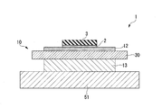
- FIG. 1 is a schematic diagram of a bonding interface between a ceramic member (ceramic substrate) and an aluminum member (aluminum plate) of a ceramic / aluminum bonded body (insulated circuit board) according to a first embodiment of the present invention. It is an expansion explanatory view of the aluminum nitride layer in the ceramics / aluminum junction object (insulation circuit board) which is a 1st embodiment of the present invention. It is an expanded explanatory view of the ceramic member (ceramics substrate) before joining in the ceramic / aluminum joined body (insulated circuit board) which is the 1st Embodiment of this invention.
- the ceramic / aluminum bonded body according to this embodiment is an insulating material formed by bonding a ceramic substrate 11 as a ceramic member and aluminum plates 22 and 23 (circuit layer 12 and metal layer 13) as aluminum members.
- the circuit board 10 is used.
- FIG. 1 shows an insulated circuit board 10 (ceramic / aluminum bonded body) and an LED module 1 using the insulated circuit board 10 according to the first embodiment of the present invention.
- the LED module 1 includes an insulating circuit board 10, an LED element 3 bonded to a surface on one side (the upper side in FIG. 1) of the insulating circuit board 10 via a bonding layer 2, and the other side of the insulating circuit board 10. And a heat sink 51 (on the lower side in FIG. 1).
- the LED element 3 is made of a semiconductor material and is a photoelectric conversion element that converts electrical energy into light.
- the light conversion efficiency of the LED element 3 is about 20 to 30%, and the remaining 70 to 80% of energy becomes heat. Therefore, the LED module 1 is required to dissipate heat efficiently.
- the bonding layer 2 for bonding the LED element 3 and the insulating circuit board 10 is made of, for example, an Au—Sn alloy solder material.
- the insulated circuit board 10 includes a ceramic substrate 30, a circuit layer 12 disposed on one surface of the ceramic substrate 30 (upper surface in FIG. 1), ceramics, and the like. And a metal layer 13 disposed on the other surface (the lower surface in FIG. 1) of the substrate 30.
- the ceramic substrate 30 is made of highly insulating Si 3 N 4 (silicon nitride).
- the thickness of the ceramic substrate 30 is set within a range of 0.2 to 1.5 mm, and is set to 0.32 mm in the present embodiment.
- the ceramic substrate 30 in this embodiment is a nitride body formed on a bonding surface between a ceramic body 31 made of silicon nitride and the circuit layer 12 and the metal layer 13 of the ceramic body 31. And an aluminum layer 36.
- the circuit layer 12 is formed by joining an aluminum plate 22 (aluminum member) made of aluminum or an aluminum alloy to one surface (the upper surface in FIG. 6) of the ceramic substrate 30.
- the aluminum plate 22 (aluminum member) constituting the circuit layer 12 for example, aluminum having a purity of 99% by mass or more (2N aluminum), aluminum having a purity of 99.9% by mass or more, and purity having a purity of 99.99% by mass or more. It is preferable to use a rolled plate such as aluminum. In this embodiment, aluminum (2N aluminum) having a purity of 99% by mass or more is used.
- the thickness of the circuit layer 12 is set in the range of 0.05 mm or more and 0.8 mm or less, for example, and is set to 0.2 mm in this embodiment.
- the metal layer 13 is formed by joining an aluminum plate 23 (aluminum member) made of aluminum or an aluminum alloy to the other surface (the lower surface in FIG. 6) of the ceramic substrate 30.
- the aluminum plate 23 (aluminum member) constituting the metal layer 13 for example, aluminum having a purity of 99% by mass or more (2N aluminum), aluminum having a purity of 99.9% by mass or more, and purity having a purity of 99.99% by mass or more. It is preferable to use a rolled plate such as aluminum. In this embodiment, aluminum (2N aluminum) having a purity of 99% by mass or more is used.
- the thickness of the metal layer 13 is set, for example, within a range of 0.05 mm or more and 1.6 mm or less, and is set to 0.6 mm in the present embodiment.
- the heat sink 51 is for cooling the insulating circuit board 10 described above, and in this embodiment, is a heat radiating plate made of a material having good thermal conductivity.
- the heat sink 51 is made of A6063 (aluminum alloy).
- the heat sink 51 is directly bonded to the metal layer 13 of the insulating circuit board 10 using a brazing material.
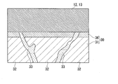
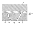
- FIG. 2 shows an enlarged explanatory view of the bonding interface between the ceramic substrate 30 and the circuit layer 12 and the metal layer 13.
- the ceramic substrate 30 includes the ceramic body 31 made of silicon nitride, and the aluminum nitride layer 36 formed on the bonding surface of the ceramic body 31 to the circuit layer 12 and the metal layer 13.
- the aluminum nitride layer 36, the circuit layer 12 and the metal layer 13 are joined.
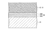
- the thickness of the aluminum nitride layer 36 is preferably in the range of 4 nm to 100 nm.
- the aluminum nitride layer 36 has a nitrogen concentration of 50 atomic% or more and 80 atomic% or less in order from the ceramic body 31 side, and a nitrogen concentration gradient in the thickness direction. And a second aluminum nitride layer 36B having a nitrogen concentration of 30 atomic% or more and less than 50 atomic% and a nitrogen concentration that is substantially constant in the thickness direction.
- the ceramic body 31 includes a silicon nitride phase 32 and a glass phase 33, and Al is present inside the glass phase 33.
- the glass phase 33 is formed by a sintering aid used when sintering the raw material of silicon nitride, and exists at the grain boundary portion between the silicon nitride phases 32 as shown in FIG.
- the glass phase 33 when analyzing the bonding interface, when the total value of Al, Si, O, and N is 100 atomic%, Si is less than 15 atomic% and O is 3 atomic%. The region within the range of 25 atomic% or less was defined as the glass phase 33. The amount of Al present in the glass phase 33 is preferably in the range of 35 atomic% to 65 atomic% when the total value of Al, Si, O, and N is 100 atomic%.
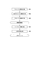
- a plate material (ceramic body 31) made of silicon nitride is prepared, and an aluminum layer 41 made of aluminum or an aluminum alloy having a thickness of 20 ⁇ m or less is formed on the surface of the ceramic body 31.
- the aluminum layer 41 is made of pure aluminum having a purity of 99% by mass or more.
- the lower limit of the thickness of the aluminum layer 41 is preferably 5 ⁇ m or more, and the lower limit of the thickness of the aluminum layer 41 is preferably 10 ⁇ m or less.
- the ceramic body 31 on which the aluminum layer 41 is formed is heat-treated at a temperature equal to or higher than the solidus temperature of the aluminum or aluminum alloy constituting the aluminum layer 41 to form the aluminum nitride layer 36.
- the aluminum nitride layer 36 is formed in the direction of eroding from the surface of the ceramic body 31 to the inside.
- the upper limit of the heat treatment temperature is preferably 750 ° C. or lower in order to suppress evaporation and the like.
- all of the aluminum layer 41 does not become the aluminum nitride layer 36, and a part thereof exists as the metal aluminum portion 38.
- An aluminum nitride layer 36 exists between the metal aluminum portion 38 and the ceramic body 31.
- the area ratio of the aluminum nitride layer 36 when the ceramic body 31 is viewed from the top is 80% or more with respect to the area where the aluminum layer 41 is formed.
- the aluminum nitride layer 36 exists between the metal aluminum part 38 and the ceramic body 31, the area of the metal aluminum part 38 and the area of the aluminum nitride layer 36 are considered to be the same.
- the aluminum plates 22 and 23 to be the circuit layer 12 and the metal layer 13 are bonded through the aluminum nitride layer 36 of the ceramic substrate 30.
- the joining means existing means such as joining using a brazing material, solid phase diffusion joining, and transient liquid phase joining (TLP) can be appropriately selected.
- TLP transient liquid phase joining
- bonding is performed using Al—Si based brazing materials 26 and 27.
- the ceramic substrate 30 and the aluminum plates 22 and 23 are laminated with Al—Si based brazing materials 26 and 27 interposed, and 1 kgf / cm 2 or more and 10 kgf / cm 2 or less (0.
- the ceramic substrate 30 and the aluminum plates 22 and 23 are joined to each other to form the circuit layer 12 and the metal layer 13 while being pressurized in a range of 098 MPa to 0.980 MPa.
- the bonding atmosphere is an inert atmosphere such as argon or nitrogen, or a vacuum atmosphere.
- the pressure is preferably in the range of 10 ⁇ 6 Pa to 10 ⁇ 3 Pa.
- the heating temperature is set in the range of 580 ° C. or more and 630 ° C. or less, and the holding time at the heating temperature is set in the range of 10 minutes or more and 45 minutes or less.
- the lower limit of the pressing load in the stacking direction is preferably 3 kgf / cm 2 or more, and more preferably 5 kgf / cm 2 or more.
- the upper limit of the pressing load in the stacking direction is preferably 8 kgf / cm 2 or less, and more preferably 7 kgf / cm 2 or less.
- the lower limit of the heating temperature is preferably 585 ° C. or higher, and more preferably 590 ° C. or higher.
- the upper limit of the heating temperature is preferably 625 ° C. or less, and more preferably 620 ° C. or less.
- the lower limit of the holding time at the heating temperature is preferably 15 minutes or more, and more preferably 20 minutes or more.
- the upper limit of the holding time at the heating temperature is preferably 40 minutes or less, and more preferably 30 minutes or less.
- the metal aluminum portion 38 (the aluminum nitride layer 36) is formed on 80% or more of the joint surface with the aluminum plates 22 and 23.
- the plates 22 and 23 are joined. For this reason, the ceramic substrate 30 and the aluminum plates 22 and 23 can be firmly bonded even under relatively low temperature conditions.
- the insulated circuit board 10 which is this embodiment is manufactured by the above processes.
- the heat sink 51 is bonded to the other surface side of the metal layer 13 of the insulating circuit substrate 10.
- the insulating circuit board 10 and the heat sink 51 are laminated through a brazing material, pressurized in the laminating direction, and inserted into a vacuum furnace for brazing. Thereby, the metal layer 13 of the insulated circuit board 10 and the heat sink 51 are joined.
- a brazing material for example, an Al—Si brazing foil having a thickness of 20 to 110 ⁇ m can be used as the brazing material, and the brazing temperature is set lower than the brazing temperature in the aluminum plate joining step S03. Is preferred.
- LED element bonding step S05 Next, the LED element 3 is joined to one surface of the circuit layer 12 of the insulating circuit board 10 by soldering. Through the above steps, the LED module 1 shown in FIG. 1 is produced.
- the ceramic substrate 30 has the ceramic body 31 and the aluminum nitride layer 36 made of silicon nitride, and the aluminum nitride layer in the glass phase 33 of the ceramic body 31. Since Al is present at the interface side portion with 36, the ceramic body 31 made of silicon nitride and the aluminum nitride layer 36 are firmly bonded. Further, since the aluminum nitride layer 36 of the ceramic substrate 30 is bonded to the circuit layer 12 (aluminum plate 22) and the metal layer 13 (aluminum plate 23), the bonding of the ceramic substrate 30 to the circuit layer 12 and the metal layer 13 is performed. High reliability. Therefore, it is possible to provide the insulated circuit board 10 having excellent bonding reliability.
- the aluminum nitride layer 36 has a nitrogen concentration of 50 atomic% or more and 80 atomic% or less in order from the ceramic body 31 side, and a nitrogen concentration gradient in the thickness direction.
- a second aluminum nitride layer 36B having a nitrogen concentration of 30 atomic% or more and less than 50 atomic% and a nitrogen concentration that is substantially constant in the thickness direction. Therefore, the aluminum nitride layer 36 is formed by the reaction of the silicon nitride of the ceramic body 31, and the ceramic body 31 made of silicon nitride and the aluminum nitride layer 36 are more firmly bonded. Thereby, even if it is a case where a thermal cycle is loaded with respect to the insulated circuit board 10, it can suppress that the joining rate of the ceramic substrate 30, the circuit layer 12, and the metal layer 13 falls.
- a metal aluminum portion 38 is formed on the bonding surface of the aluminum nitride layer 36 with the aluminum plates 22 and 23, and the metal aluminum portion 38 has the above-described surface.
- the area ratio at the joint surface is 80% or more. Therefore, the aluminum plates 22 and 23 and the metal aluminum portion 38 are bonded to each other, and the aluminum plates 22 and 23 and the ceramic substrate 30 can be bonded firmly even if the bonding temperature is set relatively low.
- Al enters the glass phase 33 of the ceramic body 31, and nitrogen (N) generated by decomposition of Si 3 N 4 of the silicon nitride phase 32 and aluminum of the aluminum layer 41
- N nitrogen
- the aluminum nitride layer 36 can be formed.
- the aluminum plate joining process S03 which joins the aluminum plates 22 and 23 through the aluminum nitride layer 36 (metal aluminum part 38) is provided, the ceramic substrate 30 and the aluminum plates 22 and 23 can be joined easily. Can do.
- the ceramic / aluminum bonded body according to the present embodiment is an insulated circuit board 110 configured by bonding a ceramic substrate 130 that is a ceramic member and an aluminum plate 122 (circuit layer 112) that is an aluminum member. Yes.
- FIG. 7 shows an insulated circuit board 110 and an LED module 101 using the insulated circuit board 110 according to the second embodiment of the present invention.
- the LED module 101 includes an insulated circuit board 110 and an LED element 3 joined to a surface on one side (upper side in FIG. 7) of the insulated circuit board 110 via a joining layer 2.
- the insulated circuit board 110 includes a ceramic substrate 130 and a circuit layer 112 disposed on one surface (upper surface in FIG. 7) of the ceramic substrate 130. Yes.
- the ceramic substrate 130 is made of highly insulating Si 3 N 4 (silicon nitride), and its thickness is set within a range of 0.2 to 1.5 mm. It is set to 32 mm.
- the ceramic substrate 130 according to the present embodiment includes a ceramic body 131 made of silicon nitride, and an aluminum oxide layer 136 formed on the bonding surface of the ceramic body 131 with the circuit layer 112. ,have.
- the circuit layer 112 is formed by joining an aluminum plate 122 (aluminum member) made of aluminum or an aluminum alloy to one surface (upper surface in FIG. 10) of the ceramic substrate 130.
- the aluminum plate 122 (aluminum member) constituting the circuit layer 112 for example, aluminum having a purity of 99% by mass or more (2N aluminum), aluminum having a purity of 99.9% by mass or more, and purity having a purity of 99.99% by mass or more. It is preferable to use a rolled plate such as aluminum. In this embodiment, aluminum (2N aluminum) having a purity of 99% by mass or more is used.
- the thickness of the circuit layer 112 is set within a range of, for example, 0.05 mm or more and 0.8 mm or less, and is set to 0.1 mm in the present embodiment.
- the ceramic substrate 130 includes the ceramic main body 131 made of silicon nitride, and the aluminum oxide layer 136 formed on the bonding surface of the ceramic main body 131 with the circuit layer 112.
- the aluminum layer 136 and the circuit layer 112 are joined.
- the thickness of the aluminum oxide layer 136 is preferably in the range of 4 nm to 100 nm.
- the ceramic body 131 includes a silicon nitride phase 132 and a glass phase 133 as shown in FIG. 8, and Al is present inside the glass phase 133.
- the glass phase 133 is formed by a sintering aid used when the silicon nitride raw material is sintered, and is present at the grain boundary portion between the silicon nitride phases 132 as shown in FIG.
- the glass phase 133 when analyzing the bonding interface, when the total value of Al, Si, O, and N is 100 atomic%, Si is less than 15 atomic% and O is 3 atomic%. The region within the range of 25 atomic% or less was defined as the glass phase 133. The amount of Al present in the glass phase 133 is preferably in the range of 35 atomic% to 65 atomic% when the total value of Al, Si, O, and N is 100 atomic%.
- a plate material (ceramic body 131) made of silicon nitride is prepared, and an aluminum layer 141 made of aluminum or an aluminum alloy having a thickness of 20 ⁇ m or less is formed on the surface of the ceramic body 131.
- the aluminum layer 141 is made of pure aluminum having a purity of 99% by mass or more.
- the ceramic body 131 on which the aluminum layer 141 is formed is heat-treated at a temperature equal to or higher than the solidus temperature of the aluminum or aluminum alloy constituting the aluminum layer 141 to form the aluminum nitride layer 136a.
- a temperature equal to or higher than the solidus temperature of the aluminum or aluminum alloy constituting the aluminum layer 141 to form the aluminum nitride layer 136a it is preferable to hold the surface of the aluminum layer 141 with a carbon plate or the like in order to prevent the molten aluminum from becoming spherical.
- the upper limit of the heat treatment temperature is preferably 750 ° C. or lower in order to suppress evaporation and the like. Note that not all of the aluminum layer 141 needs to be the aluminum nitride layer 136a, and a part of the aluminum layer 141 may exist as a metal aluminum portion.
- the ceramic body 131 on which the aluminum nitride layer 136a is formed is placed in an atmosphere furnace and subjected to an oxidation treatment to form the aluminum oxide layer 136.
- the above-described metal aluminum portion is also oxidized and becomes a part of the aluminum oxide layer 136.
- the oxidation treatment step S103 in a dry air atmosphere having a dew point of ⁇ 20 ° C. or less, the treatment temperature is in the range of 1100 ° C. or more and 1300 ° C. or less, and the holding time at the treatment temperature is in the range of 1 minute or more and 30 minutes or less. Under this condition, the aluminum nitride layer 136a is oxidized.
- the dew point of the atmosphere is preferably ⁇ 30 ° C. or lower, and more preferably ⁇ 40 ° C. or lower.
- the lower limit of the treatment temperature in the oxidation treatment step S103 is preferably 1130 ° C. or higher, and more preferably 1180 ° C. or higher.
- the upper limit of the treatment temperature in the oxidation treatment step S103 is preferably 1250 ° C. or less, and more preferably 1200 ° C. or less.
- the lower limit of the holding time at the treatment temperature in the oxidation treatment step S103 is preferably 3 minutes or more, and more preferably 5 minutes or more.
- the upper limit of the holding time at the treatment temperature is preferably 20 minutes or less, and more preferably 10 minutes or less.
- the aluminum nitride layer 136a becomes almost all the aluminum oxide layer 136.
- the aluminum plate 122 that becomes the circuit layer 112 is bonded through the aluminum oxide layer 136 of the ceramic substrate 130.
- the joining means existing means such as joining using a brazing material, solid phase diffusion joining, and transient liquid phase joining (TLP) can be appropriately selected.
- bonding is performed using an Al—Si brazing material 126 as shown in FIG.
- the ceramic substrate 130 and the aluminum plate 122 are laminated with an Al—Si brazing material 126 interposed, and 1 kgf / cm 2 or more and 10 kgf / cm 2 or less (0.098 MPa or more and 0.0.
- a circuit layer 112 is formed by charging the ceramic substrate 130 and the aluminum plate 122 in a state where the pressure is within a range of 980 MPa or less).
- the bonding conditions at this time are as follows: the vacuum condition is in the range of 10 ⁇ 6 Pa to 10 ⁇ 3 Pa, the heating temperature is in the range of 580 ° C. to 630 ° C., and the holding time at the heating temperature is 10 minutes to 45 minutes. Set within the following range.
- the insulated circuit board 110 which is this embodiment is manufactured by the above processes.
- LED element bonding step S105 Next, the LED element 3 is joined to one surface of the circuit layer 112 of the insulating circuit board 110 by soldering. Through the above steps, the LED module 101 shown in FIG. 7 is produced.
- the ceramic substrate 130 includes the ceramic body 131 and the aluminum oxide layer 136 made of silicon nitride, and the ceramic body 131 and the aluminum oxide layer. Since Al is present in the glass phase 133 of the ceramic body 131 at the interface with the ceramic body 131, the ceramic body 131 made of silicon nitride and the aluminum oxide layer 136 are firmly bonded. Further, since the aluminum oxide layer 136 and the circuit layer 112 (the aluminum plate 122) of the ceramic substrate 130 are bonded, the bonding reliability between the ceramic substrate 130 and the circuit layer 112 is high. Therefore, it is possible to provide the insulated circuit board 110 having excellent bonding reliability.
- the aluminum body 141 is formed by heating the ceramic body 131 having the aluminum layer 141 to a temperature equal to or higher than the solidus temperature of the aluminum or aluminum alloy constituting the aluminum layer 141, and the aluminum nitride layer 136a.
- Al penetrates into the glass phase 133 of the ceramic body 131, and nitrogen (N) in the silicon nitride phase 132 reacts with aluminum (Al) in the aluminum layer 141, thereby nitriding.
- An aluminum layer 136a is formed, and the aluminum oxide layer 136 can be formed by the oxidation treatment step S103.
- the aluminum plate joining process S104 which joins the aluminum plate 122 via the aluminum oxide layer 136 is provided, the ceramic substrate 130 and the aluminum plate 122 can be joined easily.
- the LED module is described by mounting the LED element on the insulating circuit board.
- a power module may be configured by mounting a power semiconductor element on the circuit layer of the insulating circuit board
- a thermoelectric module may be configured by mounting a thermoelectric element on the circuit layer of the insulating circuit board.
- the ceramic substrate and the aluminum plate have been described as being bonded using a brazing material, but the present invention is not limited to this, and may be bonded by solid phase diffusion bonding. Furthermore, bonding may be performed by a transient liquid phase bonding method (TLP) in which an additive element such as Cu or Si is fixed to the bonding surface, and these additive elements are diffused to melt and solidify. Moreover, you may join by making a joining interface into a semi-molten state.
- TLP transient liquid phase bonding method
- the aluminum layer formed on the ceramic body has been described by taking as an example an aluminum layer composed of aluminum having a purity of 99% by mass or more, it is not limited to this, and other aluminum or aluminum alloys may be used. Good.
- Mg is present in the aluminum nitride layer and the aluminum oxide layer. Since Mg is an active element, the reaction between the silicon nitride and the aluminum layer is promoted, and the aluminum nitride layer (and the aluminum oxide layer obtained by oxidizing it) is formed with a sufficient thickness. The main body and the aluminum nitride layer (aluminum oxide layer) are bonded more firmly.
- Example 1 A ceramic plate (40 mm ⁇ 40 mm ⁇ 0.32 mmt) made of silicon nitride was prepared, and an aluminum nitride layer and an aluminum oxide layer were formed on the ceramic plate by the method described in the above-described embodiment.
- an aluminum nitride layer was formed under the conditions shown in Table 1.
- an aluminum oxide layer was formed under the conditions shown in Table 2.
- the aluminum nitride layer and the aluminum oxide layer were not formed.
- the aluminum plate was joined with the method shown to Table 3, 4 with respect to the obtained ceramic substrate, and the aluminum / ceramics joined body (insulated circuit board) was manufactured.
- the aluminum / ceramic bonded body (insulated circuit board) obtained as described above was evaluated as follows.
- the glass phase has a region in which Si is less than 15 atomic% and O is in the range of 3 atomic% to 25 atomic% when the total value of Al, Si, O, and N is 100 atomic%. did.
- the evaluation results are shown in Tables 1 and 2. Moreover, the observation result of this invention example 1 is shown in FIG.
- the area ratio of the aluminum nitride layer is observed using EPMA (JXA-8539F manufactured by JEOL Ltd.) from the upper surface of the ceramic body after forming the aluminum nitride layer (aluminum nitride layer forming step S02).
- EPMA JXA-8539F manufactured by JEOL Ltd.
- the area of the metal aluminum part and the area of the aluminum nitride layer are the same, and (the area of the metal aluminum part) / Aluminum layer area ⁇ 100) was defined as the area ratio (%) of the aluminum nitride layer.
- Table 1 The results are shown in Table 1.
- the bonding rate at the interface between the ceramic substrate and the aluminum plate (circuit layer and metal layer) is evaluated using an ultrasonic flaw detector (FineSAT 200 manufactured by Hitachi Power Solutions Co., Ltd.)
- the joining rate was calculated from the following formula.
- the initial bonding area is the area to be bonded before bonding, that is, the area of the circuit layer and the metal layer (37 mm ⁇ 37 mm) in this embodiment.
- (Bonding rate) ⁇ (initial bonding area) ⁇ (peeling area) ⁇ / (initial bonding area) ⁇ 100
- the peeling is indicated by the white portion in the joint portion. Therefore, the area of the white portion is defined as the peeling area.
- Example 1-9 of the present invention in which an aluminum nitride layer is formed on the bonding surface of the ceramic plate to the aluminum plate and Al is present in the glass phase of the ceramic plate, and the bonding surface of the ceramic plate to the aluminum plate
- Example 11-19 of the present invention in which an aluminum oxide layer was formed on the ceramic plate and Al was present in the glass phase of the ceramic plate, the change in the bonding rate before and after the cooling / heating cycle was small.
- Examples 1 to 9 and 11 to 19 of the present invention regardless of the joining method of the aluminum plate, in any of the joining methods of brazing, solid phase diffusion bonding, and TLP, It was confirmed that the bonding reliability was improved. Further, as shown in Invention Examples 1 to 9 and 11 to 19, regardless of the composition of the aluminum layer and the aluminum plate, even if pure aluminum and various aluminum alloys are used, the bonding reliability of the bonded body after the thermal cycle is high. It was confirmed to improve. Further, as shown in Tables 1 and 3, it was confirmed that as the area ratio of the aluminum nitride layer was increased, the bonding reliability under a thermal cycle load was improved.
- Example 2 a ceramic plate (40 mm ⁇ 40 mm ⁇ 0.32 mmt) made of silicon nitride was prepared, and an aluminum nitride layer was formed on the ceramic plate by the method described in the above-described embodiment.
- an aluminum nitride layer was formed under the conditions shown in Table 5.
- an aluminum nitride layer was formed on the surface of the ceramic plate by sputtering.
- an aluminum plate (thickness 20 ⁇ m) having a purity of 99.99% by mass or more (4N) is used with an Al—Si brazing material (Si: 5 mass%, thickness 7 ⁇ m). Bonding was performed under the conditions of a bonding temperature of 620 ° C., a holding time of 30 min, and a pressurizing pressure of 0.098 MPa to produce an aluminum / ceramic bonded body (insulated circuit board).
- Example 2 About the aluminum / ceramic bonding body (insulated circuit board) obtained as described above, as in Example 1, the presence / absence of Al in the aluminum nitride layer, the glass phase, the area ratio of the aluminum nitride layer, and before and after the thermal cycle load The joining rate was evaluated. The evaluation results are shown in Table 5.
- the first nitridation having a nitrogen concentration of 50 atomic% to 80 atomic% and a nitrogen concentration gradient in the thickness direction.
- An aluminum layer was not formed. Further, Al was not confirmed in the glass phase of the ceramic body. And the joining rate after a cold-heat cycle load fell significantly.
- the aluminum nitride layer has a nitrogen concentration of 50 atomic percent or more and 80 atomic percent or less, and a first aluminum nitride layer having a nitrogen concentration gradient in the thickness direction, and a nitrogen concentration of 30 atomic percent or more and 50 atoms.
- the change in the bonding rate before and after the cooling cycle was small.
- the aluminum nitride layer or the aluminum oxide layer on the bonding surface of the ceramic member made of silicon nitride (Si 3 N 4 ), the aluminum member does not melt, It was confirmed that a ceramic / aluminum bonded body in which a ceramic member and an aluminum member are bonded with high reliability can be provided.
- the present invention it is possible to provide a ceramic / aluminum bonded body that is reliably bonded to a ceramic member made of silicon nitride (Si 3 N 4 ) without melting the aluminum member.
Abstract
In this ceramic/aluminum conjugate, a ceramic member and an aluminum member comprising aluminum or an aluminum alloy are bonded together. The ceramic member has a ceramic main body comprising silicon nitride, and an aluminum nitride layer or aluminum oxide layer formed on the surface of the ceramic main body where the aluminum member is to be bonded, the ceramic member being bonded to the aluminum member with the aluminum nitride layer or aluminum oxide layer interposed therebetween. The ceramic main body is provided with silicon nitride phases and a glass phase formed between the silicon nitride phases. Al is present in the portion of the glass phase of the ceramic main body on the side having the interface with the aluminum nitride layer or aluminum oxide layer.
Description
この発明は、セラミックス部材と、アルミニウム又はアルミニウム合金からなるアルミニウム部材とが接合されてなるセラミックス/アルミニウム接合体、セラミックス基板と、アルミニウム又はアルミニウム合金からなるアルミニウム板とが接合されてなる絶縁回路基板、この絶縁回路基板を備えたLEDモジュール、上述のセラミックス/アルミニウム接合体に用いられるセラミックス部材、並びに、上述のセラミックス/アルミニウム接合体の製造方法、絶縁回路基板の製造方法に関するものである。
本願は、2017年2月6日に、日本に出願された特願2017-019737号、及び2018年1月24日に、日本に出願された特願2018-009821号に基づき優先権を主張し、その内容をここに援用する。 The present invention relates to a ceramic / aluminum joined body in which a ceramic member and an aluminum member made of aluminum or an aluminum alloy are joined, an insulating circuit board in which a ceramic substrate and an aluminum plate made of aluminum or an aluminum alloy are joined, The present invention relates to an LED module including the insulating circuit board, a ceramic member used for the ceramic / aluminum bonded body, a method for manufacturing the ceramic / aluminum bonded body, and a method for manufacturing the insulating circuit board.
This application claims priority based on Japanese Patent Application No. 2017-019737 filed in Japan on February 6, 2017 and Japanese Patent Application No. 2018-009821 filed on January 24, 2018 in Japan. , The contents of which are incorporated herein.
パワーモジュール、LEDモジュール及び熱電モジュールは、絶縁層の一方の面に導電材料からなる回路層を形成した絶縁回路基板に、パワー半導体素子、LED素子及び熱電素子が接合された構造を備えている。
また、上述の絶縁回路基板においては、セラミックス基板の一方の面に導電性の優れた金属板を接合して回路層とし、また、他方の面に放熱性に優れた金属板を接合して金属層を形成した構造のものも提供されている。
さらに、回路層に搭載した素子等から発生した熱を効率的に放散させるために、絶縁回路基板の金属層側にヒートシンクを接合したヒートシンク付き絶縁回路基板も提供されている。 The power module, the LED module, and the thermoelectric module have a structure in which a power semiconductor element, an LED element, and a thermoelectric element are bonded to an insulating circuit board in which a circuit layer made of a conductive material is formed on one surface of the insulating layer.
Further, in the above-described insulated circuit board, a metal plate having excellent conductivity is bonded to one surface of the ceramic substrate to form a circuit layer, and a metal plate having excellent heat dissipation is bonded to the other surface to form a metal. A layered structure is also provided.
Furthermore, in order to efficiently dissipate heat generated from elements or the like mounted on the circuit layer, an insulating circuit board with a heat sink in which a heat sink is bonded to the metal layer side of the insulating circuit board is also provided.
例えば、特許文献1に示すパワーモジュールは、セラミックス基板の一方の面にアルミニウム板からなる回路層が形成されるとともに他方の面にアルミニウム板からなる金属層が形成された絶縁回路基板と、この回路層上にはんだ材を介して接合された半導体素子と、を備えた構造を備えている。
また、特許文献2、3に示すLEDモジュールは、セラミックスからなる基材の一方の面に導電性の回路層が形成され、絶縁基板の他方の面に放熱体が接合され、回路層上に発光素子が搭載された構造を備えている。
ここで、セラミックス基板と回路層及び金属層となるアルミニウム板を接合する際には、通常、Al-Si系ろう材が用いられている。 For example, a power module shown inPatent Document 1 includes an insulating circuit board in which a circuit layer made of an aluminum plate is formed on one surface of a ceramic substrate and a metal layer made of an aluminum plate is formed on the other surface, and this circuit. And a semiconductor element bonded to the layer via a solder material.
In addition, in the LED modules shown in Patent Documents 2 and 3, a conductive circuit layer is formed on one surface of a base material made of ceramics, and a heat radiator is bonded to the other surface of the insulating substrate, and light is emitted on the circuit layer. It has a structure in which elements are mounted.
Here, when bonding the ceramic substrate to the aluminum plate which becomes the circuit layer and the metal layer, an Al—Si based brazing material is usually used.
また、特許文献2、3に示すLEDモジュールは、セラミックスからなる基材の一方の面に導電性の回路層が形成され、絶縁基板の他方の面に放熱体が接合され、回路層上に発光素子が搭載された構造を備えている。
ここで、セラミックス基板と回路層及び金属層となるアルミニウム板を接合する際には、通常、Al-Si系ろう材が用いられている。 For example, a power module shown in
In addition, in the LED modules shown in
Here, when bonding the ceramic substrate to the aluminum plate which becomes the circuit layer and the metal layer, an Al—Si based brazing material is usually used.
ところで、上述のLEDモジュール等においては、発光素子が搭載される回路層の厚さをさらに薄くすることが求められており、例えば厚さ100μm以下のアルミニウム板をセラミックス基板に接合する場合がある。
このように厚さの薄いアルミニウム板をAl-Si系ろう材を用いて接合した場合には、回路層となるアルミニウム板にろう材のSiが拡散して融点が低下し、回路層の一部が溶融してしまうおそれがあった。 By the way, in the above-described LED module or the like, it is required to further reduce the thickness of the circuit layer on which the light emitting element is mounted. For example, an aluminum plate having a thickness of 100 μm or less may be bonded to the ceramic substrate.
When such thin aluminum plates are joined using an Al—Si brazing material, the melting point of the brazing material Si diffuses into the aluminum plate to be the circuit layer and the melting point is lowered. May melt.
回路層の溶融を抑制するために、接合温度を低下させたり、ろう材のSi量を少なくしたりした場合には、接合が不十分となり、接合信頼性が低下してしまう。このため、発熱密度が高い用途には適用することができなかった。
以上のように、従来の絶縁回路基板においては、回路層を薄く形成した場合には、回路層の溶融を抑制し、かつ、回路層とセラミックス基板との接合信頼性を向上させることは困難であった。 If the bonding temperature is lowered or the amount of Si in the brazing material is reduced in order to suppress the melting of the circuit layer, the bonding becomes insufficient and the bonding reliability is lowered. For this reason, it could not be applied to uses with high heat generation density.
As described above, in the conventional insulated circuit board, when the circuit layer is formed thin, it is difficult to suppress melting of the circuit layer and to improve the bonding reliability between the circuit layer and the ceramic substrate. there were.
また、LEDモジュールにおいて強度を確保するために、窒化ケイ素(Si3N4)からなるセラミックス基板が用いられることがある。しかしながら、窒化ケイ素(Si3N4)からなるセラミックス基板は、窒化ケイ素相と、この窒化ケイ素相の間に形成されたガラス相と、を備えており、このガラス相とアルミニウム板との接合が不十分となるため、接合強度を十分に保つことができなかった。なお、このガラス相は、窒化ケイ素の原料を焼結する際に添加される焼結助剤によって形成される。
以上のことから、窒化ケイ素(Si3N4)からなるセラミックス基板においては、窒化アルミニウム(AlN)や酸化アルミニウム(Al2O3)からなるセラミックス基板と比べて、金属板(特にアルミニウム板)との接合信頼性が劣っていた。 In order to secure strength in the LED module, a ceramic substrate made of silicon nitride (Si 3 N 4 ) may be used. However, a ceramic substrate made of silicon nitride (Si 3 N 4 ) includes a silicon nitride phase and a glass phase formed between the silicon nitride phases, and bonding between the glass phase and the aluminum plate is not possible. Since it was insufficient, the bonding strength could not be maintained sufficiently. The glass phase is formed by a sintering aid added when the silicon nitride raw material is sintered.
From the above, in a ceramic substrate made of silicon nitride (Si 3 N 4 ), compared to a ceramic substrate made of aluminum nitride (AlN) or aluminum oxide (Al 2 O 3 ), a metal plate (particularly an aluminum plate) The bonding reliability was inferior.
この発明は、前述した事情に鑑みてなされたものであって、アルミニウム部材が溶融することなく窒化ケイ素(Si3N4)からなるセラミックス部材と信頼性高く接合されたセラミックス/アルミニウム接合体、絶縁回路基板、この絶縁回路基板を備えたLEDモジュール、上述のセラミックス/アルミニウム接合体に用いられるセラミックス部材、セラミックス/アルミニウム接合体の製造方法、絶縁回路基板の製造方法を提供することを目的とする。
The present invention has been made in view of the above-described circumstances, and is a ceramic / aluminum bonded body that is bonded with a ceramic member made of silicon nitride (Si 3 N 4 ) with high reliability without melting the aluminum member. It is an object of the present invention to provide a circuit board, an LED module provided with the insulated circuit board, a ceramic member used for the ceramic / aluminum joined body, a method for producing the ceramic / aluminum joined body, and a method for producing the insulated circuit board.
上記課題を解決するために、本発明の一態様であるセラミックス/アルミニウム接合体は、セラミックス部材と、アルミニウム又はアルミニウム合金からなるアルミニウム部材とが接合されてなるセラミックス/アルミニウム接合体であって、前記セラミックス部材は、窒化ケイ素からなるセラミックス本体と、このセラミックス本体のうち前記アルミニウム部材との接合面に形成された窒化アルミニウム層又は酸化アルミニウム層と、を有し、前記窒化アルミニウム層又は前記酸化アルミニウム層を介して前記アルミニウム部材が接合されており、前記セラミックス本体は、窒化ケイ素相と、この窒化ケイ素相の間に形成されたガラス相と、を備えており、前記セラミックス本体の前記ガラス相のうち前記窒化アルミニウム層又は前記酸化アルミニウム層との界面側部分にAlが存在していることを特徴としている。
In order to solve the above problems, a ceramic / aluminum bonded body according to an aspect of the present invention is a ceramic / aluminum bonded body formed by bonding a ceramic member and an aluminum member made of aluminum or an aluminum alloy, The ceramic member has a ceramic body made of silicon nitride, and an aluminum nitride layer or an aluminum oxide layer formed on a bonding surface of the ceramic body with the aluminum member, and the aluminum nitride layer or the aluminum oxide layer The aluminum member is bonded to the ceramic body, and the ceramic body includes a silicon nitride phase and a glass phase formed between the silicon nitride phases, The aluminum nitride layer or the acid It is characterized in that Al is present in the interface portion of the aluminum layer.
この構成のセラミックス/アルミニウム接合体によれば、前記セラミックス部材は、窒化ケイ素からなるセラミックス本体と、このセラミックス本体のうち前記アルミニウム部材との接合面に形成された窒化アルミニウム層又は酸化アルミニウム層と、を有しており、前記セラミックス本体の前記ガラス相のうち前記窒化アルミニウム層又は前記酸化アルミニウム層との界面側部分にAlが存在していることから、窒化ケイ素からなるセラミックス本体と窒化アルミニウム層又は酸化アルミニウム層とが強固に結合している。
また、セラミックス部材の窒化アルミニウム層又は酸化アルミニウム層とアルミニウム部材とが接合されているので、アルミニウム部材とセラミックス部材との接合信頼性が高い。
よって、接合信頼性に優れたセラミックス/アルミニウム接合体を提供することが可能となる。 According to the ceramic / aluminum bonded body having this configuration, the ceramic member includes a ceramic body made of silicon nitride, and an aluminum nitride layer or an aluminum oxide layer formed on a bonding surface of the ceramic body with the aluminum member. And the presence of Al at the interface side portion with the aluminum nitride layer or the aluminum oxide layer in the glass phase of the ceramic body, the ceramic body made of silicon nitride and the aluminum nitride layer or The aluminum oxide layer is firmly bonded.
Moreover, since the aluminum nitride layer or the aluminum oxide layer of the ceramic member and the aluminum member are bonded, the bonding reliability between the aluminum member and the ceramic member is high.
Therefore, it is possible to provide a ceramic / aluminum bonded body excellent in bonding reliability.
ここで、本発明の一態様であるセラミックス/アルミニウム接合体においては、前記セラミックス本体のうち前記アルミニウム部材との接合面に前記窒化アルミニウム層が形成されており、前記窒化アルミニウム層は、前記セラミックス本体側から順に、窒素濃度が50原子%以上80原子%以下とされ、厚さ方向に窒素の濃度傾斜を有する第1窒化アルミニウム層と、窒素濃度が30原子%以上50原子%未満とされた第2窒化アルミニウム層と、を有していてもよい。
この場合、前記窒化アルミニウム層が、上述のように、窒素濃度が50原子%以上80原子%以下とされ、厚さ方向に窒素の濃度傾斜を有する第1窒化アルミニウム層と、窒素濃度が30原子%以上50原子%未満とされた第2窒化アルミニウム層と、を有しているので、セラミックス本体の窒化ケイ素が反応することで窒化アルミニウム層が形成されており、窒化ケイ素からなるセラミックス本体と窒化アルミニウム層とがさらに強固に結合している。これにより、セラミックス/アルミニウム接合体に対して冷熱サイクルを負荷した場合であっても、セラミックス部材とアルミニウム部材との接合率が低下することを抑制できる。 Here, in the ceramic / aluminum bonded body according to one aspect of the present invention, the aluminum nitride layer is formed on a bonding surface of the ceramic body with the aluminum member, and the aluminum nitride layer is formed of the ceramic body. In order from the side, the first aluminum nitride layer having a nitrogen concentration of 50 atomic percent or more and 80 atomic percent or less and having a nitrogen concentration gradient in the thickness direction, and a nitrogen concentration of 30 atomic percent or more and less than 50 atomic percent. And an aluminum dinitride layer.
In this case, as described above, the aluminum nitride layer has a nitrogen concentration of 50 atom% or more and 80 atom% or less, a first aluminum nitride layer having a nitrogen concentration gradient in the thickness direction, and a nitrogen concentration of 30 atoms. % And less than 50 atomic% of the second aluminum nitride layer, the silicon nitride of the ceramic body reacts to form the aluminum nitride layer, and the ceramic body made of silicon nitride and nitrided The aluminum layer is more firmly bonded. Thereby, even if it is a case where a thermal cycle is loaded with respect to a ceramic / aluminum joined body, it can suppress that the joining rate of a ceramic member and an aluminum member falls.
本発明の一態様である絶縁回路基板は、セラミックス基板と、アルミニウム又はアルミニウム合金からなるアルミニウム板とが接合されてなる絶縁回路基板であって、前記セラミックス基板は、窒化ケイ素からなるセラミックス本体と、このセラミックス本体のうち前記アルミニウム板との接合面に形成された窒化アルミニウム層又は酸化アルミニウム層と、を有し、前記窒化アルミニウム層又は前記酸化アルミニウム層を介して前記アルミニウム板が接合されており、前記セラミックス本体は、窒化ケイ素相と、この窒化ケイ素相の間に形成されたガラス相と、を備えており、前記セラミックス本体の前記ガラス相のうち前記窒化アルミニウム層又は前記酸化アルミニウム層との界面側部分にAlが存在していることを特徴としている。
An insulated circuit board according to an aspect of the present invention is an insulated circuit board formed by bonding a ceramic substrate and an aluminum plate made of aluminum or an aluminum alloy, the ceramic substrate comprising a ceramic body made of silicon nitride, An aluminum nitride layer or an aluminum oxide layer formed on a bonding surface of the ceramic body with the aluminum plate, and the aluminum plate is bonded via the aluminum nitride layer or the aluminum oxide layer, The ceramic body includes a silicon nitride phase and a glass phase formed between the silicon nitride phases, and an interface between the glass phase of the ceramic body and the aluminum nitride layer or the aluminum oxide layer. It is characterized in that Al is present on the side portion.
この構成の絶縁回路基板によれば、前記セラミックス基板が、窒化ケイ素からなるセラミックス本体と、窒化アルミニウム層又は酸化アルミニウム層と、を有しており、前記セラミックス本体の前記ガラス相のうち前記窒化アルミニウム層又は前記酸化アルミニウム層との界面側部分にAlが存在していることから、窒化ケイ素からなるセラミックス本体と窒化アルミニウム層又は酸化アルミニウム層とが強固に結合している。
また、セラミックス基板の窒化アルミニウム層又は酸化アルミニウム層とアルミニウム板とが接合されているので、アルミニウム板とセラミックス基板との接合信頼性に優れた絶縁回路基板を提供することが可能となる。 According to the insulated circuit board having this configuration, the ceramic substrate has a ceramic body made of silicon nitride, and an aluminum nitride layer or an aluminum oxide layer, and the aluminum nitride in the glass phase of the ceramic body. Since Al is present at the interface or the interface side portion with the aluminum oxide layer, the ceramic body made of silicon nitride and the aluminum nitride layer or aluminum oxide layer are firmly bonded.
Further, since the aluminum nitride layer or aluminum oxide layer of the ceramic substrate and the aluminum plate are bonded, it is possible to provide an insulating circuit substrate having excellent bonding reliability between the aluminum plate and the ceramic substrate.
ここで、本発明の一態様である絶縁回路基板においては、前記セラミックス本体のうち前記アルミニウム板との接合面に前記窒化アルミニウム層が形成されており、前記窒化アルミニウム層は、前記セラミックス本体側から順に、窒素濃度が50原子%以上80原子%以下とされ、厚さ方向に窒素の濃度傾斜を有する第1窒化アルミニウム層と、窒素濃度が30原子%以上50原子%未満とされた第2窒化アルミニウム層と、を有していてもよい。
この場合、前記窒化アルミニウム層が、上述のように、窒素濃度が50原子%以上80原子%以下とされ、厚さ方向に窒素の濃度傾斜を有する第1窒化アルミニウム層と、窒素濃度が30原子%以上50原子%未満とされた第2窒化アルミニウム層と、を有しているので、セラミックス本体の窒化ケイ素が反応することで窒化アルミニウム層が形成されており、窒化ケイ素からなるセラミックス本体と窒化アルミニウム層とがさらに強固に結合している。これにより、絶縁回路基板に対して冷熱サイクルを負荷した場合であっても、セラミックス基板とアルミニウム板との接合率が低下することを抑制できる。 Here, in the insulated circuit board according to one aspect of the present invention, the aluminum nitride layer is formed on the bonding surface of the ceramic body with the aluminum plate, and the aluminum nitride layer is formed from the ceramic body side. In order, the first aluminum nitride layer having a nitrogen concentration of 50 atomic percent or more and 80 atomic percent or less and a nitrogen concentration gradient in the thickness direction, and the second nitriding in which the nitrogen concentration is 30 atomic percent or more and less than 50 atomic percent. And an aluminum layer.
In this case, as described above, the aluminum nitride layer has a nitrogen concentration of 50 atom% or more and 80 atom% or less, a first aluminum nitride layer having a nitrogen concentration gradient in the thickness direction, and a nitrogen concentration of 30 atoms. % And less than 50 atomic% of the second aluminum nitride layer, the silicon nitride of the ceramic body reacts to form the aluminum nitride layer, and the ceramic body made of silicon nitride and nitrided The aluminum layer is more firmly bonded. Thereby, even if it is a case where a thermal cycle is loaded with respect to an insulated circuit board, it can suppress that the joining rate of a ceramic substrate and an aluminum plate falls.
本発明の一態様であるLEDモジュールは、上述の絶縁回路基板と、前記アルミニウム板の一方の面側に接合されたLED素子と、を備えていることを特徴としている。
この構成のLEDモジュールにおいては、セラミックス基板とアルミニウム板との接合信頼性に優れた絶縁回路基板を用いているので、冷熱サイクルが負荷された場合であっても、剥離等の不具合が生じることを抑制できる。 An LED module which is one embodiment of the present invention includes the above-described insulating circuit board and an LED element bonded to one surface side of the aluminum plate.
In the LED module having this configuration, since an insulating circuit substrate having excellent bonding reliability between the ceramic substrate and the aluminum plate is used, problems such as peeling may occur even when a thermal cycle is applied. Can be suppressed.
本発明の一態様であるセラミックス部材は、窒化ケイ素からなるセラミックス本体と、このセラミックス本体の表面に形成された窒化アルミニウム層又は酸化アルミニウム層と、を備え、前記セラミックス本体は、窒化ケイ素相と、この窒化ケイ素相の間に形成されたガラス相と、を備えており、前記セラミックス本体の前記ガラス相のうち前記窒化アルミニウム層又は前記酸化アルミニウム層との界面側部分にAlが存在していることを特徴としている。
A ceramic member according to one aspect of the present invention includes a ceramic body made of silicon nitride, and an aluminum nitride layer or an aluminum oxide layer formed on the surface of the ceramic body, the ceramic body having a silicon nitride phase, A glass phase formed between the silicon nitride phases, and Al is present in an interface side portion with the aluminum nitride layer or the aluminum oxide layer in the glass phase of the ceramic body. It is characterized by.
この構成のセラミックス部材によれば、前記セラミックス本体の前記ガラス相のうち前記窒化アルミニウム層又は前記酸化アルミニウム層との界面側部分にAlが存在しているので、窒化ケイ素からなるセラミックス本体と窒化アルミニウム層又は酸化アルミニウム層とが強固に結合している。
また、窒化アルミニウム層又は酸化アルミニウム層を備えているので、アルミニウム部材と良好に接合することができる。 According to the ceramic member having this structure, since Al exists in the interface side portion of the glass phase of the ceramic body with the aluminum nitride layer or the aluminum oxide layer, the ceramic body made of silicon nitride and the aluminum nitride The layer or the aluminum oxide layer is firmly bonded.
Moreover, since the aluminum nitride layer or the aluminum oxide layer is provided, it can be satisfactorily bonded to the aluminum member.
ここで、本発明の一態様であるセラミックス部材においては、前記セラミックス本体の表面に前記窒化アルミニウム層が形成されており、前記窒化アルミニウム層は、前記セラミックス本体側から順に、窒素濃度が50原子%以上80原子%以下とされ、厚さ方向に窒素の濃度傾斜を有する第1窒化アルミニウム層と、窒素濃度が30原子%以上50原子%未満とされた第2窒化アルミニウム層と、を有している構成としてもよい。
この場合、前記窒化アルミニウム層が、上述のように、窒素濃度が50原子%以上80原子%以下とされ、厚さ方向に窒素の濃度傾斜を有する第1窒化アルミニウム層と、窒素濃度が30原子%以上50原子%未満とされた第2窒化アルミニウム層と、を有しているので、セラミックス本体の窒化ケイ素が反応することで窒化アルミニウム層が形成されており、窒化ケイ素からなるセラミックス本体と窒化アルミニウム層とがさらに強固に結合している。 Here, in the ceramic member according to one aspect of the present invention, the aluminum nitride layer is formed on the surface of the ceramic body, and the aluminum nitride layer has a nitrogen concentration of 50 atomic% in order from the ceramic body side. A first aluminum nitride layer having a nitrogen concentration gradient in the thickness direction, and a second aluminum nitride layer having a nitrogen concentration of 30 atomic percent or more and less than 50 atomic percent. It is good also as composition which has.
In this case, as described above, the aluminum nitride layer has a nitrogen concentration of 50 atom% or more and 80 atom% or less, a first aluminum nitride layer having a nitrogen concentration gradient in the thickness direction, and a nitrogen concentration of 30 atoms. % And less than 50 atomic% of the second aluminum nitride layer, the silicon nitride of the ceramic body reacts to form the aluminum nitride layer, and the ceramic body made of silicon nitride and nitrided The aluminum layer is more firmly bonded.
また、本発明の一態様であるセラミックス部材においては、前記セラミックス本体の表面に前記窒化アルミニウム層が形成されており、この窒化アルミニウム層のうち前記セラミックス本体とは反対側の面に、金属アルミニウム部が形成されている構成としてもよい。
この場合、金属アルミニウム部を介してアルニウム部材を接合することが可能となり、アルミニウム部材をさらに容易に接合することができる。なお、金属アルミニウム部は、窒化アルミニウム層のうち前記セラミックス本体とは反対側の面の全体に形成されている必要はなく、部分的に形成されていてもよい。 In the ceramic member according to one aspect of the present invention, the aluminum nitride layer is formed on a surface of the ceramic body, and a metal aluminum portion is formed on a surface of the aluminum nitride layer opposite to the ceramic body. It is good also as a structure in which is formed.
In this case, it becomes possible to join the aluminum member through the metal aluminum part, and the aluminum member can be joined more easily. In addition, the metal aluminum part does not need to be formed in the whole surface on the opposite side to the said ceramic main body among aluminum nitride layers, and may be formed partially.
本発明の一態様であるセラミックス/アルミニウム接合体の製造方法は、上述のセラミックス/アルミニウム接合体を製造するセラミックス/アルミニウム接合体の製造方法であって、窒化ケイ素からなるセラミックス本体の表面に、厚さ20μm以下のアルミニウム層を形成するアルミニウム層形成工程と、前記アルミニウム層が形成されたセラミックス本体を、前記アルミニウム層の固相線温度以上の温度まで加熱し、窒化アルミニウム層を形成する窒化アルミニウム層形成工程と、前記窒化アルミニウム層を介してアルミニウム部材を接合するアルミニウム部材接合工程と、を備えていることを特徴としている。
A method for manufacturing a ceramic / aluminum bonded body according to an aspect of the present invention is a method for manufacturing a ceramic / aluminum bonded body for manufacturing the above-described ceramic / aluminum bonded body. An aluminum layer forming step for forming an aluminum layer having a thickness of 20 μm or less, and an aluminum nitride layer for forming an aluminum nitride layer by heating the ceramic body on which the aluminum layer is formed to a temperature not lower than the solidus temperature of the aluminum layer And a forming step and an aluminum member joining step for joining the aluminum member through the aluminum nitride layer.
この構成のセラミックス/アルミニウム接合体の製造方法によれば、窒化ケイ素からなるセラミックス本体の表面に、厚さ20μm以下のアルミニウム層を形成するアルミニウム層形成工程と、前記アルミニウム層が形成されたセラミックス本体を、前記アルミニウム層の固相線温度以上の温度まで加熱し、窒化アルミニウム層を形成する窒化アルミニウム層形成工程と、を備えている。そのため、この窒化アルミニウム層形成工程において、セラミックス本体のガラス相にAlが侵入するとともに、窒化ケイ素相のSi3N4が分解して生じた窒素とアルミニウム層とが反応することで、窒化アルミニウム層が形成される。なお、アルミニウム層の一部が残存することで、窒化アルミニウム層のうち前記セラミックス本体とは反対側の面に、金属アルミニウム部が形成されることもある。
そして、前記窒化アルミニウム層を介してアルミニウム部材を接合するアルミニウム部材接合工程を備えているので、セラミックス部材とアルミニウム部材とを容易に接合することができる。
よって、接合信頼性に優れたセラミックス/アルミニウム接合体を製造することが可能となる。 According to the method for manufacturing a ceramic / aluminum bonded body having this configuration, an aluminum layer forming step of forming an aluminum layer having a thickness of 20 μm or less on the surface of a ceramic body made of silicon nitride, and the ceramic body on which the aluminum layer is formed Is heated to a temperature equal to or higher than the solidus temperature of the aluminum layer to form an aluminum nitride layer. Therefore, in this aluminum nitride layer forming step, Al penetrates into the glass phase of the ceramic body, and nitrogen generated by decomposition of Si 3 N 4 in the silicon nitride phase reacts with the aluminum layer, so that the aluminum nitride layer Is formed. In addition, when a part of aluminum layer remains, a metal aluminum part may be formed in the surface on the opposite side to the said ceramic main body among aluminum nitride layers.
And since the aluminum member joining process which joins an aluminum member through the said aluminum nitride layer is provided, a ceramic member and an aluminum member can be joined easily.
Therefore, it is possible to manufacture a ceramic / aluminum bonded body having excellent bonding reliability.
ここで、本発明の一態様であるセラミックス/アルミニウム接合体の製造方法においては、前記窒化アルミニウム層を酸化させて酸化アルミニウム層を形成する酸化処理工程と、前記酸化アルミニウム層を介してアルミニウム部材を接合するアルミニウム部材接合工程と、を備えていてもよい。
この場合、窒化アルミニウム層を酸化させることにより、酸化アルミニウム層を形成することができる。なお、窒化アルミニウム層のうち前記セラミックス本体とは反対側の面に金属アルミニウム部が形成されていた場合には、酸化処理工程によってこの金属アルミニウム部も酸化アルミニウム層となる。
また、前記酸化アルミニウム層を介してアルミニウム部材を接合するアルミニウム部材接合工程を備えているので、セラミックス部材とアルミニウム部材とを容易に接合することができる。
よって、接合信頼性に優れたセラミックス/アルミニウム接合体を製造することが可能となる。 Here, in the method for manufacturing a ceramic / aluminum bonded body according to one aspect of the present invention, an oxidation treatment step of oxidizing the aluminum nitride layer to form an aluminum oxide layer, and an aluminum member through the aluminum oxide layer And an aluminum member joining step for joining.
In this case, the aluminum oxide layer can be formed by oxidizing the aluminum nitride layer. In addition, when the metal aluminum part is formed in the surface on the opposite side to the said ceramic main body among aluminum nitride layers, this metal aluminum part also turns into an aluminum oxide layer by an oxidation treatment process.
Moreover, since the aluminum member joining process which joins an aluminum member through the said aluminum oxide layer is provided, a ceramic member and an aluminum member can be joined easily.
Therefore, it is possible to manufacture a ceramic / aluminum bonded body having excellent bonding reliability.
本発明の一態様である絶縁回路基板の製造方法は、上述の絶縁回路基板を製造する絶縁回路基板の製造方法であって、窒化ケイ素からなるセラミックス本体の表面に、厚さ20μm以下のアルミニウム層を形成するアルミニウム層形成工程と、前記アルミニウム層が形成されたセラミックス本体を、前記アルミニウム層の固相線温度以上の温度まで加熱し、窒化アルミニウム層を形成する窒化アルミニウム層形成工程と、前記窒化アルミニウム層を介してアルミニウム板を接合するアルミニウム板接合工程と、を備えていることを特徴としている。
An insulating circuit board manufacturing method according to an aspect of the present invention is an insulating circuit board manufacturing method for manufacturing the above-described insulating circuit board, wherein an aluminum layer having a thickness of 20 μm or less is formed on a surface of a ceramic body made of silicon nitride. Forming the aluminum layer, heating the ceramic body on which the aluminum layer is formed to a temperature equal to or higher than the solidus temperature of the aluminum layer to form an aluminum nitride layer, and the nitriding An aluminum plate joining step for joining the aluminum plates via the aluminum layer.
この構成の絶縁回路基板の製造方法によれば、窒化ケイ素からなるセラミックス本体の表面に、厚さ20μm以下のアルミニウム層を形成するアルミニウム層形成工程と、前記アルミニウム層が形成されたセラミックス本体を、前記アルミニウム層の固相線温度以上の温度まで加熱し、窒化アルミニウム層を形成する窒化アルミニウム層形成工程と、を備えている。そのため、この窒化アルミニウム層形成工程において、セラミックス本体のガラス相にAlが侵入するとともに、窒化ケイ素相のSi3N4が分解して生じた窒素とアルミニウム層とが反応することで、窒化アルミニウム層が形成される。なお、アルミニウム層の一部が残存することで、窒化アルミニウム層のうち前記セラミックス本体とは反対側の面に、金属アルミニウム部が形成されることもある。
そして、前記窒化アルミニウム層を介してアルミニウム板を接合するアルミニウム板接合工程を備えているので、セラミックス基板とアルミニウム板とを容易に接合することができる。
よって、接合信頼性に優れた絶縁回路基板を製造することが可能となる。 According to the method for manufacturing an insulated circuit board having this configuration, an aluminum layer forming step of forming an aluminum layer having a thickness of 20 μm or less on the surface of a ceramic body made of silicon nitride, and a ceramic body on which the aluminum layer is formed, An aluminum nitride layer forming step of heating the aluminum layer to a temperature equal to or higher than the solidus temperature of the aluminum layer to form an aluminum nitride layer. Therefore, in this aluminum nitride layer forming step, Al penetrates into the glass phase of the ceramic body, and nitrogen generated by decomposition of Si 3 N 4 in the silicon nitride phase reacts with the aluminum layer, so that the aluminum nitride layer Is formed. In addition, when a part of aluminum layer remains, a metal aluminum part may be formed in the surface on the opposite side to the said ceramic main body among aluminum nitride layers.
And since the aluminum plate joining process which joins an aluminum plate through the said aluminum nitride layer is provided, a ceramic substrate and an aluminum plate can be joined easily.
Therefore, it is possible to manufacture an insulated circuit board having excellent bonding reliability.
ここで、本発明の一態様である絶縁回路基板の製造方法においては、前記窒化アルミニウム層を酸化させて酸化アルミニウム層を形成する酸化処理工程と、前記酸化アルミニウム層を介してアルミニウム板を接合するアルミニウム板接合工程と、を備えていてもよい。
この場合、窒化アルミニウム層を酸化させることにより、酸化アルミニウム層を形成することができる。なお、窒化アルミニウム層のうち前記セラミックス本体とは反対側の面に金属アルミニウム部が形成されていた場合には、酸化処理工程によってこの金属アルミニウム部も酸化アルミニウム層となる。
また、前記酸化アルミニウム層を介してアルミニウム板を接合するアルミニウム板接合工程を備えているので、セラミックス基板とアルミニウム板とを容易に接合することができる。
よって、接合信頼性に優れた絶縁回路基板を製造することが可能となる。 Here, in the method for manufacturing an insulated circuit board according to one embodiment of the present invention, an aluminum plate is bonded through the oxidation process step of oxidizing the aluminum nitride layer to form an aluminum oxide layer, and the aluminum oxide layer. An aluminum plate joining step.
In this case, the aluminum oxide layer can be formed by oxidizing the aluminum nitride layer. In addition, when the metal aluminum part is formed in the surface on the opposite side to the said ceramic main body among aluminum nitride layers, this metal aluminum part also turns into an aluminum oxide layer by an oxidation treatment process.
Moreover, since the aluminum plate joining process which joins an aluminum plate through the said aluminum oxide layer is provided, a ceramic substrate and an aluminum plate can be joined easily.
Therefore, it is possible to manufacture an insulated circuit board having excellent bonding reliability.
本発明によれば、アルミニウム部材が溶融することなく窒化ケイ素(Si3N4)からなるセラミックス部材と信頼性高く接合されたセラミックス/アルミニウム接合体、絶縁回路基板、この絶縁回路基板を備えたLEDモジュール、上述のセラミックス/アルミニウム接合体に用いられるセラミックス部材、セラミックス/アルミニウム接合体の製造方法、絶縁回路基板の製造方法を提供することができる。
According to the present invention, a ceramic / aluminum bonded body that is reliably bonded to a ceramic member made of silicon nitride (Si 3 N 4 ) without melting the aluminum member, an insulating circuit board, and an LED including the insulating circuit board A module, a ceramic member used for the above-described ceramic / aluminum bonded body, a method for manufacturing a ceramic / aluminum bonded body, and a method for manufacturing an insulated circuit board can be provided.
以下に、本発明の実施形態について、添付した図面を参照して説明する。
Embodiments of the present invention will be described below with reference to the accompanying drawings.
(第1の実施形態)
まず、本発明の第1の実施形態について、図1から図6を参照して説明する。
本実施形態に係るセラミックス/アルミニウム接合体は、セラミックス部材であるセラミックス基板11と、アルミニウム部材であるアルミニウム板22、23(回路層12、金属層13)とが接合されることにより構成された絶縁回路基板10とされている。 (First embodiment)
First, a first embodiment of the present invention will be described with reference to FIGS.
The ceramic / aluminum bonded body according to this embodiment is an insulating material formed by bonding a ceramic substrate 11 as a ceramic member andaluminum plates 22 and 23 (circuit layer 12 and metal layer 13) as aluminum members. The circuit board 10 is used.
まず、本発明の第1の実施形態について、図1から図6を参照して説明する。
本実施形態に係るセラミックス/アルミニウム接合体は、セラミックス部材であるセラミックス基板11と、アルミニウム部材であるアルミニウム板22、23(回路層12、金属層13)とが接合されることにより構成された絶縁回路基板10とされている。 (First embodiment)
First, a first embodiment of the present invention will be described with reference to FIGS.
The ceramic / aluminum bonded body according to this embodiment is an insulating material formed by bonding a ceramic substrate 11 as a ceramic member and
図1に、本発明の第1の実施形態である絶縁回路基板10(セラミックス/アルミニウム接合体)及びこの絶縁回路基板10を用いたLEDモジュール1を示す。
このLEDモジュール1は、絶縁回路基板10と、この絶縁回路基板10の一方側(図1において上側)の面に接合層2を介して接合されたLED素子3と、絶縁回路基板10の他方側(図1において下側)に配置されたヒートシンク51と、を備えている。 FIG. 1 shows an insulated circuit board 10 (ceramic / aluminum bonded body) and anLED module 1 using the insulated circuit board 10 according to the first embodiment of the present invention.
TheLED module 1 includes an insulating circuit board 10, an LED element 3 bonded to a surface on one side (the upper side in FIG. 1) of the insulating circuit board 10 via a bonding layer 2, and the other side of the insulating circuit board 10. And a heat sink 51 (on the lower side in FIG. 1).
このLEDモジュール1は、絶縁回路基板10と、この絶縁回路基板10の一方側(図1において上側)の面に接合層2を介して接合されたLED素子3と、絶縁回路基板10の他方側(図1において下側)に配置されたヒートシンク51と、を備えている。 FIG. 1 shows an insulated circuit board 10 (ceramic / aluminum bonded body) and an
The
LED素子3は、半導体材料で構成されており、電気エネルギーを光に変換する光電変換素子である。なお、LED素子3の光変換効率は20~30%程度であり、残りの70~80%のエネルギーは熱となるため、LEDモジュール1においては効率的に熱を放散させることが求められる。
ここで、このLED素子3と絶縁回路基板10とを接合する接合層2は、例えばAu-Sn合金はんだ材等とされている。 TheLED element 3 is made of a semiconductor material and is a photoelectric conversion element that converts electrical energy into light. The light conversion efficiency of the LED element 3 is about 20 to 30%, and the remaining 70 to 80% of energy becomes heat. Therefore, the LED module 1 is required to dissipate heat efficiently.
Here, thebonding layer 2 for bonding the LED element 3 and the insulating circuit board 10 is made of, for example, an Au—Sn alloy solder material.
ここで、このLED素子3と絶縁回路基板10とを接合する接合層2は、例えばAu-Sn合金はんだ材等とされている。 The
Here, the
そして、本実施形態に係る絶縁回路基板10は、図1に示すように、セラミックス基板30と、このセラミックス基板30の一方の面(図1において上面)に配設された回路層12と、セラミックス基板30の他方の面(図1において下面)に配設された金属層13と、を備えている。
As shown in FIG. 1, the insulated circuit board 10 according to the present embodiment includes a ceramic substrate 30, a circuit layer 12 disposed on one surface of the ceramic substrate 30 (upper surface in FIG. 1), ceramics, and the like. And a metal layer 13 disposed on the other surface (the lower surface in FIG. 1) of the substrate 30.
セラミックス基板30は、絶縁性の高いSi3N4(窒化珪素)で構成されている。ここで、セラミックス基板30の厚さは、0.2~1.5mmの範囲内に設定されており、本実施形態では、0.32mmに設定されている。
ここで、本実施形態におけるセラミックス基板30は、図4に示すように、窒化ケイ素からなるセラミックス本体31と、このセラミックス本体31のうち回路層12及び金属層13との接合面に形成された窒化アルミニウム層36と、を有している。 Theceramic substrate 30 is made of highly insulating Si 3 N 4 (silicon nitride). Here, the thickness of the ceramic substrate 30 is set within a range of 0.2 to 1.5 mm, and is set to 0.32 mm in the present embodiment.
Here, as shown in FIG. 4, theceramic substrate 30 in this embodiment is a nitride body formed on a bonding surface between a ceramic body 31 made of silicon nitride and the circuit layer 12 and the metal layer 13 of the ceramic body 31. And an aluminum layer 36.
ここで、本実施形態におけるセラミックス基板30は、図4に示すように、窒化ケイ素からなるセラミックス本体31と、このセラミックス本体31のうち回路層12及び金属層13との接合面に形成された窒化アルミニウム層36と、を有している。 The
Here, as shown in FIG. 4, the
回路層12は、図6に示すように、セラミックス基板30の一方の面(図6において上面)にアルミニウム又はアルミニウム合金からなるアルミニウム板22(アルミニウム部材)が接合されることで形成されている。回路層12を構成するアルミニウム板22(アルミニウム部材)としては、例えば、純度が99質量%以上のアルミニウム(2Nアルミニウム)や純度99.9質量%以上のアルミニウムや純度が99.99質量%以上のアルミニウム等の圧延板が用いることが好ましく、本実施形態では、純度が99質量%以上のアルミニウム(2Nアルミニウム)を用いている。なお、回路層12の厚さは、例えば0.05mm以上0.8mm以下の範囲内に設定されており、本実施形態では、0.2mmに設定されている。
As shown in FIG. 6, the circuit layer 12 is formed by joining an aluminum plate 22 (aluminum member) made of aluminum or an aluminum alloy to one surface (the upper surface in FIG. 6) of the ceramic substrate 30. As the aluminum plate 22 (aluminum member) constituting the circuit layer 12, for example, aluminum having a purity of 99% by mass or more (2N aluminum), aluminum having a purity of 99.9% by mass or more, and purity having a purity of 99.99% by mass or more. It is preferable to use a rolled plate such as aluminum. In this embodiment, aluminum (2N aluminum) having a purity of 99% by mass or more is used. In addition, the thickness of the circuit layer 12 is set in the range of 0.05 mm or more and 0.8 mm or less, for example, and is set to 0.2 mm in this embodiment.
金属層13は、図6に示すように、セラミックス基板30の他方の面(図6において下面)にアルミニウム又はアルミニウム合金からなるアルミニウム板23(アルミニウム部材)が接合されることで形成されている。金属層13を構成するアルミニウム板23(アルミニウム部材)としては、例えば、純度が99質量%以上のアルミニウム(2Nアルミニウム)や純度99.9質量%以上のアルミニウムや純度が99.99質量%以上のアルミニウム等の圧延板が用いることが好ましく、本実施形態では、純度が99質量%以上のアルミニウム(2Nアルミニウム)を用いている。なお、金属層13の厚さは、例えば0.05mm以上1.6mm以下の範囲内に設定されており、本実施形態では、0.6mmに設定されている。
As shown in FIG. 6, the metal layer 13 is formed by joining an aluminum plate 23 (aluminum member) made of aluminum or an aluminum alloy to the other surface (the lower surface in FIG. 6) of the ceramic substrate 30. As the aluminum plate 23 (aluminum member) constituting the metal layer 13, for example, aluminum having a purity of 99% by mass or more (2N aluminum), aluminum having a purity of 99.9% by mass or more, and purity having a purity of 99.99% by mass or more. It is preferable to use a rolled plate such as aluminum. In this embodiment, aluminum (2N aluminum) having a purity of 99% by mass or more is used. Note that the thickness of the metal layer 13 is set, for example, within a range of 0.05 mm or more and 1.6 mm or less, and is set to 0.6 mm in the present embodiment.
ヒートシンク51は、前述の絶縁回路基板10を冷却するためのものであり、本実施形態においては、熱伝導性が良好な材質で構成された放熱板とされている。本実施形態においては、ヒートシンク51は、A6063(アルミニウム合金)で構成されている。
このヒートシンク51は、本実施形態においては、絶縁回路基板10の金属層13にろう材を用いて直接接合されている。 Theheat sink 51 is for cooling the insulating circuit board 10 described above, and in this embodiment, is a heat radiating plate made of a material having good thermal conductivity. In the present embodiment, the heat sink 51 is made of A6063 (aluminum alloy).
In this embodiment, theheat sink 51 is directly bonded to the metal layer 13 of the insulating circuit board 10 using a brazing material.
このヒートシンク51は、本実施形態においては、絶縁回路基板10の金属層13にろう材を用いて直接接合されている。 The
In this embodiment, the
ここで、セラミックス基板30と回路層12及び金属層13との接合界面の拡大説明図を図2に示す。
セラミックス基板30は、上述のように、窒化ケイ素からなるセラミックス本体31と、このセラミックス本体31のうち回路層12及び金属層13との接合面に形成された窒化アルミニウム層36と、を有しており、この窒化アルミニウム層36と回路層12及び金属層13とが接合された構造とされている。
ここで、窒化アルミニウム層36の厚さは4nm以上100nm以下の範囲内とされていることが好ましい。 Here, FIG. 2 shows an enlarged explanatory view of the bonding interface between theceramic substrate 30 and the circuit layer 12 and the metal layer 13.
As described above, theceramic substrate 30 includes the ceramic body 31 made of silicon nitride, and the aluminum nitride layer 36 formed on the bonding surface of the ceramic body 31 to the circuit layer 12 and the metal layer 13. The aluminum nitride layer 36, the circuit layer 12 and the metal layer 13 are joined.
Here, the thickness of thealuminum nitride layer 36 is preferably in the range of 4 nm to 100 nm.
セラミックス基板30は、上述のように、窒化ケイ素からなるセラミックス本体31と、このセラミックス本体31のうち回路層12及び金属層13との接合面に形成された窒化アルミニウム層36と、を有しており、この窒化アルミニウム層36と回路層12及び金属層13とが接合された構造とされている。
ここで、窒化アルミニウム層36の厚さは4nm以上100nm以下の範囲内とされていることが好ましい。 Here, FIG. 2 shows an enlarged explanatory view of the bonding interface between the
As described above, the
Here, the thickness of the
また、本実施形態においては、図3に示すように、窒化アルミニウム層36は、セラミックス本体31側から順に、窒素濃度が50原子%以上80原子%以下とされ、厚さ方向に窒素の濃度傾斜を有する第1窒化アルミニウム層36Aと、窒素濃度が30原子%以上50原子%未満とされ、窒素濃度が厚さ方向でほぼ一定である第2窒化アルミニウム層36Bと、を有している。
In the present embodiment, as shown in FIG. 3, the aluminum nitride layer 36 has a nitrogen concentration of 50 atomic% or more and 80 atomic% or less in order from the ceramic body 31 side, and a nitrogen concentration gradient in the thickness direction. And a second aluminum nitride layer 36B having a nitrogen concentration of 30 atomic% or more and less than 50 atomic% and a nitrogen concentration that is substantially constant in the thickness direction.
そして、セラミックス本体31は、図2に示すように、窒化ケイ素相32とガラス相33とを備えており、このガラス相33の内部にAlが存在している。ガラス相33は、窒化ケイ素の原料を焼結する際に用いられる焼結助剤によって形成されるものであり、図2に示すように、窒化ケイ素相32同士の粒界部分に存在する。
As shown in FIG. 2, the ceramic body 31 includes a silicon nitride phase 32 and a glass phase 33, and Al is present inside the glass phase 33. The glass phase 33 is formed by a sintering aid used when sintering the raw material of silicon nitride, and exists at the grain boundary portion between the silicon nitride phases 32 as shown in FIG.
ここで、本実施形態においては、接合界面を分析した際に、Al,Si,O,Nの合計値を100原子%とした際に、Siが15原子%未満、且つ、Oが3原子%以上25原子%以下の範囲内の領域をガラス相33とした。
このガラス相33中に存在するAl量は、Al,Si,O,Nの合計値を100原子%とした際に、35原子%以上65原子%以下の範囲内であることが好ましい。 Here, in this embodiment, when analyzing the bonding interface, when the total value of Al, Si, O, and N is 100 atomic%, Si is less than 15 atomic% and O is 3 atomic%. The region within the range of 25 atomic% or less was defined as theglass phase 33.
The amount of Al present in theglass phase 33 is preferably in the range of 35 atomic% to 65 atomic% when the total value of Al, Si, O, and N is 100 atomic%.
このガラス相33中に存在するAl量は、Al,Si,O,Nの合計値を100原子%とした際に、35原子%以上65原子%以下の範囲内であることが好ましい。 Here, in this embodiment, when analyzing the bonding interface, when the total value of Al, Si, O, and N is 100 atomic%, Si is less than 15 atomic% and O is 3 atomic%. The region within the range of 25 atomic% or less was defined as the
The amount of Al present in the
次に、上述した本実施形態である絶縁回路基板10の製造方法について、図5及び図6を参照して説明する。
Next, a method for manufacturing the insulated circuit board 10 according to the present embodiment described above will be described with reference to FIGS.
(アルミニウム層形成工程S01)
窒化ケイ素からなる板材(セラミックス本体31)を準備し、このセラミックス本体31の表面に厚さ20μm以下のアルミニウム又はアルミニウム合金からなるアルミニウム層41を形成する。本実施形態では、アルミニウム層41は、純度99質量%以上の純アルミニウムで構成されたものとした。
ここで、厚さ1μm未満のアルミニウム層41を形成する場合には、スパッタ等の成膜技術を適用することが好ましい。また、厚さ1μm以上20μm以下のアルミニウム層41を形成する場合には、圧延箔等をセラミックス本体31の表面に積層することが好ましい。
なお、アルミニウム層41の厚さの下限は5μm以上とすることが好ましく、アルミニウム層41の厚さの下限は10μm以下とすることが好ましい。 (Aluminum layer forming step S01)
A plate material (ceramic body 31) made of silicon nitride is prepared, and analuminum layer 41 made of aluminum or an aluminum alloy having a thickness of 20 μm or less is formed on the surface of the ceramic body 31. In the present embodiment, the aluminum layer 41 is made of pure aluminum having a purity of 99% by mass or more.
Here, when thealuminum layer 41 having a thickness of less than 1 μm is formed, it is preferable to apply a film forming technique such as sputtering. Moreover, when forming the aluminum layer 41 with a thickness of 1 μm or more and 20 μm or less, it is preferable to laminate a rolled foil or the like on the surface of the ceramic body 31.
Note that the lower limit of the thickness of thealuminum layer 41 is preferably 5 μm or more, and the lower limit of the thickness of the aluminum layer 41 is preferably 10 μm or less.
窒化ケイ素からなる板材(セラミックス本体31)を準備し、このセラミックス本体31の表面に厚さ20μm以下のアルミニウム又はアルミニウム合金からなるアルミニウム層41を形成する。本実施形態では、アルミニウム層41は、純度99質量%以上の純アルミニウムで構成されたものとした。
ここで、厚さ1μm未満のアルミニウム層41を形成する場合には、スパッタ等の成膜技術を適用することが好ましい。また、厚さ1μm以上20μm以下のアルミニウム層41を形成する場合には、圧延箔等をセラミックス本体31の表面に積層することが好ましい。
なお、アルミニウム層41の厚さの下限は5μm以上とすることが好ましく、アルミニウム層41の厚さの下限は10μm以下とすることが好ましい。 (Aluminum layer forming step S01)
A plate material (ceramic body 31) made of silicon nitride is prepared, and an
Here, when the
Note that the lower limit of the thickness of the
(窒化アルミニウム層形成工程S02)
次に、アルミニウム層41が形成されたセラミックス本体31を、アルミニウム層41を構成するアルミニウム又はアルミニウム合金の固相線温度以上の温度で熱処理を行い、窒化アルミニウム層36を形成する。窒化アルミニウム層36はセラミックス本体31の表面から内部に浸食する方向に形成される。
ここで、熱処理を行う際には、溶融したアルミニウムが球状になることを抑制するために、アルミニウム層41の表面をカーボン板等で押さえておくことが好ましい。また、熱処理温度の上限は、蒸発等を抑制するために、750℃以下とすることが好ましい。 (Aluminum nitride layer forming step S02)
Next, theceramic body 31 on which the aluminum layer 41 is formed is heat-treated at a temperature equal to or higher than the solidus temperature of the aluminum or aluminum alloy constituting the aluminum layer 41 to form the aluminum nitride layer 36. The aluminum nitride layer 36 is formed in the direction of eroding from the surface of the ceramic body 31 to the inside.
Here, when performing the heat treatment, it is preferable to hold the surface of thealuminum layer 41 with a carbon plate or the like in order to prevent the molten aluminum from becoming spherical. The upper limit of the heat treatment temperature is preferably 750 ° C. or lower in order to suppress evaporation and the like.
次に、アルミニウム層41が形成されたセラミックス本体31を、アルミニウム層41を構成するアルミニウム又はアルミニウム合金の固相線温度以上の温度で熱処理を行い、窒化アルミニウム層36を形成する。窒化アルミニウム層36はセラミックス本体31の表面から内部に浸食する方向に形成される。
ここで、熱処理を行う際には、溶融したアルミニウムが球状になることを抑制するために、アルミニウム層41の表面をカーボン板等で押さえておくことが好ましい。また、熱処理温度の上限は、蒸発等を抑制するために、750℃以下とすることが好ましい。 (Aluminum nitride layer forming step S02)
Next, the
Here, when performing the heat treatment, it is preferable to hold the surface of the
なお、本実施形態においては、図4に示すように、アルミニウム層41の全てが窒化アルミニウム層36にならず、一部が金属アルミニウム部38として存在している。そして、金属アルミニウム部38とセラミックス本体31の間には窒化アルミニウム層36が存在している。
ここで、セラミックス本体31を上面視した場合における、窒化アルミニウム層36の面積率はアルミニウム層41を形成した面積に対して80%以上とされている。本実施形態では、金属アルミニウム部38とセラミックス本体31の間には窒化アルミニウム層36が存在していることから、金属アルミニウム部38の面積と窒化アルミニウム層36の面積は同じであるとみなす。 In the present embodiment, as shown in FIG. 4, all of thealuminum layer 41 does not become the aluminum nitride layer 36, and a part thereof exists as the metal aluminum portion 38. An aluminum nitride layer 36 exists between the metal aluminum portion 38 and the ceramic body 31.
Here, the area ratio of thealuminum nitride layer 36 when the ceramic body 31 is viewed from the top is 80% or more with respect to the area where the aluminum layer 41 is formed. In this embodiment, since the aluminum nitride layer 36 exists between the metal aluminum part 38 and the ceramic body 31, the area of the metal aluminum part 38 and the area of the aluminum nitride layer 36 are considered to be the same.
ここで、セラミックス本体31を上面視した場合における、窒化アルミニウム層36の面積率はアルミニウム層41を形成した面積に対して80%以上とされている。本実施形態では、金属アルミニウム部38とセラミックス本体31の間には窒化アルミニウム層36が存在していることから、金属アルミニウム部38の面積と窒化アルミニウム層36の面積は同じであるとみなす。 In the present embodiment, as shown in FIG. 4, all of the
Here, the area ratio of the
(アルミニウム板接合工程S03)
次に、セラミックス基板30の窒化アルミニウム層36を介して、回路層12及び金属層13となるアルミニウム板22,23を接合する。ここで、接合手段としては、ろう材を用いた接合、固相拡散接合、過渡液相接合(TLP)等の既存の手段を適宜選択することができる。本実施形態では、図6に示すように、Al-Si系ろう材26,27を用いて接合している。 (Aluminum plate joining step S03)
Next, the aluminum plates 22 and 23 to be the circuit layer 12 and the metal layer 13 are bonded through the aluminum nitride layer 36 of the ceramic substrate 30. Here, as the joining means, existing means such as joining using a brazing material, solid phase diffusion joining, and transient liquid phase joining (TLP) can be appropriately selected. In this embodiment, as shown in FIG. 6, bonding is performed using Al—Si based brazing materials 26 and 27.
次に、セラミックス基板30の窒化アルミニウム層36を介して、回路層12及び金属層13となるアルミニウム板22,23を接合する。ここで、接合手段としては、ろう材を用いた接合、固相拡散接合、過渡液相接合(TLP)等の既存の手段を適宜選択することができる。本実施形態では、図6に示すように、Al-Si系ろう材26,27を用いて接合している。 (Aluminum plate joining step S03)
Next, the
具体的には、セラミックス基板30とアルミニウム板22,23とを、Al-Si系のろう材26、27を介在させて積層し、積層方向に1kgf/cm2以上10kgf/cm2以下(0.098MPa以上0.980MPa以下)の範囲で加圧した状態で真空加熱炉に装入し、セラミックス基板30とアルミニウム板22,23とを接合し、回路層12及び金属層13を形成する。
このときの接合条件として、接合雰囲気は、アルゴンや窒素等の不活性雰囲気や、真空雰囲気等で行う。真空雰囲気の場合は、10-6Pa以上10-3Pa以下の範囲内とするとよい。加熱温度は580℃以上630℃以下の範囲内、上記加熱温度での保持時間は10分以上45分以下の範囲内に設定する。 Specifically, theceramic substrate 30 and the aluminum plates 22 and 23 are laminated with Al—Si based brazing materials 26 and 27 interposed, and 1 kgf / cm 2 or more and 10 kgf / cm 2 or less (0. The ceramic substrate 30 and the aluminum plates 22 and 23 are joined to each other to form the circuit layer 12 and the metal layer 13 while being pressurized in a range of 098 MPa to 0.980 MPa.
As a bonding condition at this time, the bonding atmosphere is an inert atmosphere such as argon or nitrogen, or a vacuum atmosphere. In the case of a vacuum atmosphere, the pressure is preferably in the range of 10 −6 Pa to 10 −3 Pa. The heating temperature is set in the range of 580 ° C. or more and 630 ° C. or less, and the holding time at the heating temperature is set in the range of 10 minutes or more and 45 minutes or less.
このときの接合条件として、接合雰囲気は、アルゴンや窒素等の不活性雰囲気や、真空雰囲気等で行う。真空雰囲気の場合は、10-6Pa以上10-3Pa以下の範囲内とするとよい。加熱温度は580℃以上630℃以下の範囲内、上記加熱温度での保持時間は10分以上45分以下の範囲内に設定する。 Specifically, the
As a bonding condition at this time, the bonding atmosphere is an inert atmosphere such as argon or nitrogen, or a vacuum atmosphere. In the case of a vacuum atmosphere, the pressure is preferably in the range of 10 −6 Pa to 10 −3 Pa. The heating temperature is set in the range of 580 ° C. or more and 630 ° C. or less, and the holding time at the heating temperature is set in the range of 10 minutes or more and 45 minutes or less.
ここで、積層方向の加圧荷重の下限は3kgf/cm2以上とすることが好ましく、5kgf/cm2以上とすることがさらに好ましい。一方、積層方向の加圧荷重の上限は8kgf/cm2以下とすることが好ましく、7kgf/cm2以下とすることがさらに好ましい。
また、加熱温度の下限は、585℃以上とすることが好ましく、590℃以上とすることがさらに好ましい。一方、加熱温度の上限は、625℃以下とすることが好ましく、620℃以下とすることがさらに好ましい。
さらに、加熱温度での保持時間の下限は、15分以上とすることが好ましく、20分以上とすることがさらに好ましい。一方、加熱温度での保持時間の上限は、40分以下とすることが好ましく、30分以下とすることがさらに好ましい。 Here, the lower limit of the pressing load in the stacking direction is preferably 3 kgf / cm 2 or more, and more preferably 5 kgf / cm 2 or more. On the other hand, the upper limit of the pressing load in the stacking direction is preferably 8 kgf / cm 2 or less, and more preferably 7 kgf / cm 2 or less.
The lower limit of the heating temperature is preferably 585 ° C. or higher, and more preferably 590 ° C. or higher. On the other hand, the upper limit of the heating temperature is preferably 625 ° C. or less, and more preferably 620 ° C. or less.
Furthermore, the lower limit of the holding time at the heating temperature is preferably 15 minutes or more, and more preferably 20 minutes or more. On the other hand, the upper limit of the holding time at the heating temperature is preferably 40 minutes or less, and more preferably 30 minutes or less.
また、本実施形態では、上述のように、アルミニウム板22,23との接合面の80%以上に金属アルミニウム部38(窒化アルミニウム層36)が形成されているので、この金属アルミニウム部38とアルミニウム板22,23とを接合する。このため、比較的低温条件であっても、セラミックス基板30とアルミニウム板22,23とを強固に接合することができる。
In the present embodiment, as described above, the metal aluminum portion 38 (the aluminum nitride layer 36) is formed on 80% or more of the joint surface with the aluminum plates 22 and 23. The plates 22 and 23 are joined. For this reason, the ceramic substrate 30 and the aluminum plates 22 and 23 can be firmly bonded even under relatively low temperature conditions.
以上のような工程により、本実施形態である絶縁回路基板10が製造される。
The insulated circuit board 10 which is this embodiment is manufactured by the above processes.
(ヒートシンク接合工程S04)
次に、絶縁回路基板10の金属層13の他方の面側に、ヒートシンク51を接合する。
絶縁回路基板10とヒートシンク51とを、ろう材を介して積層し、積層方向に加圧するとともに真空炉内に装入してろう付けを行う。これにより、絶縁回路基板10の金属層13とヒートシンク51とを接合する。このとき、ろう材としては、例えば、厚さ20~110μmのAl-Si系ろう材箔を用いることができ、ろう付け温度は、アルミニウム板接合工程S03におけるろう付け温度よりも低温に設定することが好ましい。 (Heat sink joining step S04)
Next, theheat sink 51 is bonded to the other surface side of the metal layer 13 of the insulating circuit substrate 10.
The insulatingcircuit board 10 and the heat sink 51 are laminated through a brazing material, pressurized in the laminating direction, and inserted into a vacuum furnace for brazing. Thereby, the metal layer 13 of the insulated circuit board 10 and the heat sink 51 are joined. At this time, for example, an Al—Si brazing foil having a thickness of 20 to 110 μm can be used as the brazing material, and the brazing temperature is set lower than the brazing temperature in the aluminum plate joining step S03. Is preferred.
次に、絶縁回路基板10の金属層13の他方の面側に、ヒートシンク51を接合する。
絶縁回路基板10とヒートシンク51とを、ろう材を介して積層し、積層方向に加圧するとともに真空炉内に装入してろう付けを行う。これにより、絶縁回路基板10の金属層13とヒートシンク51とを接合する。このとき、ろう材としては、例えば、厚さ20~110μmのAl-Si系ろう材箔を用いることができ、ろう付け温度は、アルミニウム板接合工程S03におけるろう付け温度よりも低温に設定することが好ましい。 (Heat sink joining step S04)
Next, the
The insulating
(LED素子接合工程S05)
次に、絶縁回路基板10の回路層12の一方の面に、LED素子3をはんだ付けにより接合する。
以上の工程により、図1に示すLEDモジュール1が製出される。 (LED element bonding step S05)
Next, theLED element 3 is joined to one surface of the circuit layer 12 of the insulating circuit board 10 by soldering.
Through the above steps, theLED module 1 shown in FIG. 1 is produced.
次に、絶縁回路基板10の回路層12の一方の面に、LED素子3をはんだ付けにより接合する。
以上の工程により、図1に示すLEDモジュール1が製出される。 (LED element bonding step S05)
Next, the
Through the above steps, the
以上のような構成の絶縁回路基板10によれば、セラミックス基板30が、窒化ケイ素からなるセラミックス本体31と窒化アルミニウム層36とを有しており、セラミックス本体31のガラス相33のうち窒化アルミニウム層36との界面側部分にAlが存在していることから、窒化ケイ素からなるセラミックス本体31と窒化アルミニウム層36とが強固に結合している。また、セラミックス基板30の窒化アルミニウム層36と回路層12(アルミニウム板22)及び金属層13(アルミニウム板23)とが接合されているので、セラミックス基板30と回路層12及び金属層13との接合信頼性が高い。よって、接合信頼性に優れた絶縁回路基板10を提供することが可能となる。
According to the insulated circuit board 10 configured as described above, the ceramic substrate 30 has the ceramic body 31 and the aluminum nitride layer 36 made of silicon nitride, and the aluminum nitride layer in the glass phase 33 of the ceramic body 31. Since Al is present at the interface side portion with 36, the ceramic body 31 made of silicon nitride and the aluminum nitride layer 36 are firmly bonded. Further, since the aluminum nitride layer 36 of the ceramic substrate 30 is bonded to the circuit layer 12 (aluminum plate 22) and the metal layer 13 (aluminum plate 23), the bonding of the ceramic substrate 30 to the circuit layer 12 and the metal layer 13 is performed. High reliability. Therefore, it is possible to provide the insulated circuit board 10 having excellent bonding reliability.
さらに、本実施形態においては、図3に示すように、窒化アルミニウム層36が、セラミックス本体31側から順に、窒素濃度が50原子%以上80原子%以下とされ、厚さ方向に窒素の濃度傾斜を有する第1窒化アルミニウム層36Aと、窒素濃度が30原子%以上50原子%未満とされ、窒素濃度が厚さ方向でほぼ一定である第2窒化アルミニウム層36Bと、を有している。そのため、セラミックス本体31の窒化ケイ素が反応することで窒化アルミニウム層36が形成されており、窒化ケイ素からなるセラミックス本体31と窒化アルミニウム層36とがさらに強固に結合している。これにより、絶縁回路基板10に対して冷熱サイクルを負荷した場合であっても、セラミックス基板30と回路層12及び金属層13との接合率が低下することを抑制できる。
Furthermore, in the present embodiment, as shown in FIG. 3, the aluminum nitride layer 36 has a nitrogen concentration of 50 atomic% or more and 80 atomic% or less in order from the ceramic body 31 side, and a nitrogen concentration gradient in the thickness direction. And a second aluminum nitride layer 36B having a nitrogen concentration of 30 atomic% or more and less than 50 atomic% and a nitrogen concentration that is substantially constant in the thickness direction. Therefore, the aluminum nitride layer 36 is formed by the reaction of the silicon nitride of the ceramic body 31, and the ceramic body 31 made of silicon nitride and the aluminum nitride layer 36 are more firmly bonded. Thereby, even if it is a case where a thermal cycle is loaded with respect to the insulated circuit board 10, it can suppress that the joining rate of the ceramic substrate 30, the circuit layer 12, and the metal layer 13 falls.
また、本実施形態においては、接合前のセラミックス基板30において、窒化アルミニウム層36のうちアルミニウム板22,23のとの接合面に金属アルミニウム部38が形成されており、この金属アルミニウム部38の前記接合面における面積率が80%以上とされている。そのため、アルミニウム板22,23と金属アルミニウム部38とがアルミニウム同士の接合となり、接合温度を比較的低く設定しても、アルミニウム板22,23とセラミックス基板30とを強固に接合することができる。
In the present embodiment, in the ceramic substrate 30 before bonding, a metal aluminum portion 38 is formed on the bonding surface of the aluminum nitride layer 36 with the aluminum plates 22 and 23, and the metal aluminum portion 38 has the above-described surface. The area ratio at the joint surface is 80% or more. Therefore, the aluminum plates 22 and 23 and the metal aluminum portion 38 are bonded to each other, and the aluminum plates 22 and 23 and the ceramic substrate 30 can be bonded firmly even if the bonding temperature is set relatively low.
さらに、本実施形態である絶縁回路基板10の製造方法によれば、窒化ケイ素からなるセラミックス本体31の表面に、厚さ20μm以下のアルミニウム層41を形成するアルミニウム層形成工程S01と、アルミニウム層41が形成されたセラミックス本体31を、アルミニウム層41を構成するアルミニウム又はアルミニウム合金の固相線温度以上の温度まで加熱し、窒化アルミニウム層36を形成する窒化アルミニウム層形成工程S02と、を備えている。そのため、この窒化アルミニウム層形成工程S02において、セラミックス本体31のガラス相33にAlが侵入するとともに、窒化ケイ素相32のSi3N4が分解して生じた窒素(N)とアルミニウム層41のアルミニウム(Al)とが反応することで、窒化アルミニウム層36を形成することができる。
そして、窒化アルミニウム層36(金属アルミニウム部38)を介してアルミニウム板22,23を接合するアルミニウム板接合工程S03を備えているので、セラミックス基板30とアルミニウム板22,23とを容易に接合することができる。 Furthermore, according to the method for manufacturing the insulatedcircuit board 10 of the present embodiment, the aluminum layer forming step S01 for forming the aluminum layer 41 having a thickness of 20 μm or less on the surface of the ceramic body 31 made of silicon nitride, and the aluminum layer 41 An aluminum nitride layer forming step S02 for forming the aluminum nitride layer 36 by heating the ceramic body 31 on which the aluminum layer 41 is formed to a temperature equal to or higher than the solidus temperature of the aluminum or aluminum alloy constituting the aluminum layer 41. . Therefore, in this aluminum nitride layer forming step S02, Al enters the glass phase 33 of the ceramic body 31, and nitrogen (N) generated by decomposition of Si 3 N 4 of the silicon nitride phase 32 and aluminum of the aluminum layer 41 By reacting with (Al), the aluminum nitride layer 36 can be formed.
And since the aluminum plate joining process S03 which joins the aluminum plates 22 and 23 through the aluminum nitride layer 36 (metal aluminum part 38) is provided, the ceramic substrate 30 and the aluminum plates 22 and 23 can be joined easily. Can do.
そして、窒化アルミニウム層36(金属アルミニウム部38)を介してアルミニウム板22,23を接合するアルミニウム板接合工程S03を備えているので、セラミックス基板30とアルミニウム板22,23とを容易に接合することができる。 Furthermore, according to the method for manufacturing the insulated
And since the aluminum plate joining process S03 which joins the
(第2の実施形態)
次に、本発明の第2の実施形態について、図7から図10を参照して説明する。なお、第1の実施形態と同一の部材には、同一の符号を付して詳細な説明を省略する。
本実施形態に係るセラミックス/アルミニウム接合体は、セラミックス部材であるセラミックス基板130と、アルミニウム部材であるアルミニウム板122(回路層112)とが接合されることにより構成された絶縁回路基板110とされている。 (Second Embodiment)
Next, a second embodiment of the present invention will be described with reference to FIGS. In addition, the same code | symbol is attached | subjected to the member same as 1st Embodiment, and detailed description is abbreviate | omitted.
The ceramic / aluminum bonded body according to the present embodiment is an insulatedcircuit board 110 configured by bonding a ceramic substrate 130 that is a ceramic member and an aluminum plate 122 (circuit layer 112) that is an aluminum member. Yes.
次に、本発明の第2の実施形態について、図7から図10を参照して説明する。なお、第1の実施形態と同一の部材には、同一の符号を付して詳細な説明を省略する。
本実施形態に係るセラミックス/アルミニウム接合体は、セラミックス部材であるセラミックス基板130と、アルミニウム部材であるアルミニウム板122(回路層112)とが接合されることにより構成された絶縁回路基板110とされている。 (Second Embodiment)
Next, a second embodiment of the present invention will be described with reference to FIGS. In addition, the same code | symbol is attached | subjected to the member same as 1st Embodiment, and detailed description is abbreviate | omitted.
The ceramic / aluminum bonded body according to the present embodiment is an insulated
図7に、本発明の第2の実施形態である絶縁回路基板110及びこの絶縁回路基板110を用いたLEDモジュール101を示す。
このLEDモジュール101は、絶縁回路基板110と、この絶縁回路基板110の一方側(図7において上側)の面に接合層2を介して接合されたLED素子3と、を備えている。 FIG. 7 shows aninsulated circuit board 110 and an LED module 101 using the insulated circuit board 110 according to the second embodiment of the present invention.
TheLED module 101 includes an insulated circuit board 110 and an LED element 3 joined to a surface on one side (upper side in FIG. 7) of the insulated circuit board 110 via a joining layer 2.
このLEDモジュール101は、絶縁回路基板110と、この絶縁回路基板110の一方側(図7において上側)の面に接合層2を介して接合されたLED素子3と、を備えている。 FIG. 7 shows an
The
本実施形態に係る絶縁回路基板110は、図7に示すように、セラミックス基板130と、このセラミックス基板130の一方の面(図7において上面)に配設された回路層112と、を備えている。
As shown in FIG. 7, the insulated circuit board 110 according to the present embodiment includes a ceramic substrate 130 and a circuit layer 112 disposed on one surface (upper surface in FIG. 7) of the ceramic substrate 130. Yes.
セラミックス基板130は、絶縁性の高いSi3N4(窒化珪素)で構成されており、その厚さが0.2~1.5mmの範囲内に設定されており、本実施形態では、0.32mmに設定されている。
ここで、本実施形態におけるセラミックス基板130は、図8に示すように、窒化ケイ素からなるセラミックス本体131と、このセラミックス本体131のうち回路層112との接合面に形成された酸化アルミニウム層136と、を有している。 Theceramic substrate 130 is made of highly insulating Si 3 N 4 (silicon nitride), and its thickness is set within a range of 0.2 to 1.5 mm. It is set to 32 mm.
Here, as shown in FIG. 8, theceramic substrate 130 according to the present embodiment includes a ceramic body 131 made of silicon nitride, and an aluminum oxide layer 136 formed on the bonding surface of the ceramic body 131 with the circuit layer 112. ,have.
ここで、本実施形態におけるセラミックス基板130は、図8に示すように、窒化ケイ素からなるセラミックス本体131と、このセラミックス本体131のうち回路層112との接合面に形成された酸化アルミニウム層136と、を有している。 The
Here, as shown in FIG. 8, the
回路層112は、図10に示すように、セラミックス基板130の一方の面(図10において上面)にアルミニウム又はアルミニウム合金からなるアルミニウム板122(アルミニウム部材)が接合されることで形成されている。回路層112を構成するアルミニウム板122(アルミニウム部材)としては、例えば、純度が99質量%以上のアルミニウム(2Nアルミニウム)や純度99.9質量%以上のアルミニウムや純度が99.99質量%以上のアルミニウム等の圧延板が用いることが好ましく、本実施形態では、純度が99質量%以上のアルミニウム(2Nアルミニウム)を用いている。なお、回路層112の厚さは、例えば0.05mm以上0.8mm以下の範囲内に設定されており、本実施形態では、0.1mmに設定されている。
As shown in FIG. 10, the circuit layer 112 is formed by joining an aluminum plate 122 (aluminum member) made of aluminum or an aluminum alloy to one surface (upper surface in FIG. 10) of the ceramic substrate 130. As the aluminum plate 122 (aluminum member) constituting the circuit layer 112, for example, aluminum having a purity of 99% by mass or more (2N aluminum), aluminum having a purity of 99.9% by mass or more, and purity having a purity of 99.99% by mass or more. It is preferable to use a rolled plate such as aluminum. In this embodiment, aluminum (2N aluminum) having a purity of 99% by mass or more is used. Note that the thickness of the circuit layer 112 is set within a range of, for example, 0.05 mm or more and 0.8 mm or less, and is set to 0.1 mm in the present embodiment.
ここで、セラミックス基板130と回路層112との接合界面の拡大説明図を図8に示す。
セラミックス基板130は、上述のように、窒化ケイ素からなるセラミックス本体131と、このセラミックス本体131のうち回路層112との接合面に形成された酸化アルミニウム層136と、を有しており、この酸化アルミニウム層136と回路層112とが接合された構造とされている。
ここで、酸化アルミニウム層136の厚さは4nm以上100nm以下の範囲内とされていることが好ましい。 Here, an enlarged explanatory view of the bonding interface between theceramic substrate 130 and the circuit layer 112 is shown in FIG.
As described above, theceramic substrate 130 includes the ceramic main body 131 made of silicon nitride, and the aluminum oxide layer 136 formed on the bonding surface of the ceramic main body 131 with the circuit layer 112. The aluminum layer 136 and the circuit layer 112 are joined.
Here, the thickness of thealuminum oxide layer 136 is preferably in the range of 4 nm to 100 nm.
セラミックス基板130は、上述のように、窒化ケイ素からなるセラミックス本体131と、このセラミックス本体131のうち回路層112との接合面に形成された酸化アルミニウム層136と、を有しており、この酸化アルミニウム層136と回路層112とが接合された構造とされている。
ここで、酸化アルミニウム層136の厚さは4nm以上100nm以下の範囲内とされていることが好ましい。 Here, an enlarged explanatory view of the bonding interface between the
As described above, the
Here, the thickness of the
そして、セラミックス本体131は、図8に示すように、窒化ケイ素相132とガラス相133とを備えており、このガラス相133の内部にAlが存在している。ガラス相133は、窒化ケイ素の原料を焼結する際に用いられる焼結助剤によって形成されるものであり、図8に示すように、窒化ケイ素相132同士の粒界部分に存在する。
The ceramic body 131 includes a silicon nitride phase 132 and a glass phase 133 as shown in FIG. 8, and Al is present inside the glass phase 133. The glass phase 133 is formed by a sintering aid used when the silicon nitride raw material is sintered, and is present at the grain boundary portion between the silicon nitride phases 132 as shown in FIG.
ここで、本実施形態においては、接合界面を分析した際に、Al,Si,O,Nの合計値を100原子%とした際に、Siが15原子%未満、且つ、Oが3原子%以上25原子%以下の範囲内の領域をガラス相133とした。
このガラス相133中に存在するAl量は、Al,Si,O,Nの合計値を100原子%とした際に、35原子%以上65原子%以下の範囲内であることが好ましい。 Here, in this embodiment, when analyzing the bonding interface, when the total value of Al, Si, O, and N is 100 atomic%, Si is less than 15 atomic% and O is 3 atomic%. The region within the range of 25 atomic% or less was defined as theglass phase 133.
The amount of Al present in theglass phase 133 is preferably in the range of 35 atomic% to 65 atomic% when the total value of Al, Si, O, and N is 100 atomic%.
このガラス相133中に存在するAl量は、Al,Si,O,Nの合計値を100原子%とした際に、35原子%以上65原子%以下の範囲内であることが好ましい。 Here, in this embodiment, when analyzing the bonding interface, when the total value of Al, Si, O, and N is 100 atomic%, Si is less than 15 atomic% and O is 3 atomic%. The region within the range of 25 atomic% or less was defined as the
The amount of Al present in the
次に、上述した本実施形態である絶縁回路基板110の製造方法について、図9及び図10を参照して説明する。
Next, a method for manufacturing the insulated circuit board 110 according to the present embodiment described above will be described with reference to FIGS.
(アルミニウム層形成工程S101)
窒化ケイ素からなる板材(セラミックス本体131)を準備し、このセラミックス本体131の表面に厚さ20μm以下のアルミニウム又はアルミニウム合金からなるアルミニウム層141を形成する。本実施形態では、アルミニウム層141は、純度99質量%以上の純アルミニウムで構成されたものとした。 (Aluminum layer forming step S101)
A plate material (ceramic body 131) made of silicon nitride is prepared, and analuminum layer 141 made of aluminum or an aluminum alloy having a thickness of 20 μm or less is formed on the surface of the ceramic body 131. In the present embodiment, the aluminum layer 141 is made of pure aluminum having a purity of 99% by mass or more.
窒化ケイ素からなる板材(セラミックス本体131)を準備し、このセラミックス本体131の表面に厚さ20μm以下のアルミニウム又はアルミニウム合金からなるアルミニウム層141を形成する。本実施形態では、アルミニウム層141は、純度99質量%以上の純アルミニウムで構成されたものとした。 (Aluminum layer forming step S101)
A plate material (ceramic body 131) made of silicon nitride is prepared, and an
(窒化アルミニウム層形成工程S102)
次に、アルミニウム層141が形成されたセラミックス本体131を、アルミニウム層141を構成するアルミニウム又はアルミニウム合金の固相線温度以上の温度で熱処理を行い、窒化アルミニウム層136aを形成する。
ここで、熱処理を行う際には、溶融したアルミニウムが球状になることを抑制するために、アルミニウム層141の表面をカーボン板等で押さえておくことが好ましい。また、熱処理温度の上限は、蒸発等を抑制するために、750℃以下とすることが好ましい。
なお、アルミニウム層141の全てが窒化アルミニウム層136aになる必要はなく、一部のアルミニウム層141が金属アルミニウム部として存在していてもよい。 (Aluminum nitride layer forming step S102)
Next, theceramic body 131 on which the aluminum layer 141 is formed is heat-treated at a temperature equal to or higher than the solidus temperature of the aluminum or aluminum alloy constituting the aluminum layer 141 to form the aluminum nitride layer 136a.
Here, when performing the heat treatment, it is preferable to hold the surface of thealuminum layer 141 with a carbon plate or the like in order to prevent the molten aluminum from becoming spherical. The upper limit of the heat treatment temperature is preferably 750 ° C. or lower in order to suppress evaporation and the like.
Note that not all of thealuminum layer 141 needs to be the aluminum nitride layer 136a, and a part of the aluminum layer 141 may exist as a metal aluminum portion.
次に、アルミニウム層141が形成されたセラミックス本体131を、アルミニウム層141を構成するアルミニウム又はアルミニウム合金の固相線温度以上の温度で熱処理を行い、窒化アルミニウム層136aを形成する。
ここで、熱処理を行う際には、溶融したアルミニウムが球状になることを抑制するために、アルミニウム層141の表面をカーボン板等で押さえておくことが好ましい。また、熱処理温度の上限は、蒸発等を抑制するために、750℃以下とすることが好ましい。
なお、アルミニウム層141の全てが窒化アルミニウム層136aになる必要はなく、一部のアルミニウム層141が金属アルミニウム部として存在していてもよい。 (Aluminum nitride layer forming step S102)
Next, the
Here, when performing the heat treatment, it is preferable to hold the surface of the
Note that not all of the
(酸化処理工程S103)
次に、窒化アルミニウム層136aが形成されたセラミックス本体131を雰囲気炉に装入して酸化処理を行い、酸化アルミニウム層136を形成する。このとき、上述の金属アルミニウム部も酸化され、酸化アルミニウム層136の一部となる。
酸化処理工程S103においては、露点-20℃以下の乾燥空気雰囲気中で、処理温度:1100℃以上1300℃以下の範囲内、上述の処理温度での保持時間:1分以上30分以下の範囲内の条件で、窒化アルミニウム層136aの酸化処理を実施している。 (Oxidation treatment step S103)
Next, theceramic body 131 on which the aluminum nitride layer 136a is formed is placed in an atmosphere furnace and subjected to an oxidation treatment to form the aluminum oxide layer 136. At this time, the above-described metal aluminum portion is also oxidized and becomes a part of the aluminum oxide layer 136.
In the oxidation treatment step S103, in a dry air atmosphere having a dew point of −20 ° C. or less, the treatment temperature is in the range of 1100 ° C. or more and 1300 ° C. or less, and the holding time at the treatment temperature is in the range of 1 minute or more and 30 minutes or less. Under this condition, thealuminum nitride layer 136a is oxidized.
次に、窒化アルミニウム層136aが形成されたセラミックス本体131を雰囲気炉に装入して酸化処理を行い、酸化アルミニウム層136を形成する。このとき、上述の金属アルミニウム部も酸化され、酸化アルミニウム層136の一部となる。
酸化処理工程S103においては、露点-20℃以下の乾燥空気雰囲気中で、処理温度:1100℃以上1300℃以下の範囲内、上述の処理温度での保持時間:1分以上30分以下の範囲内の条件で、窒化アルミニウム層136aの酸化処理を実施している。 (Oxidation treatment step S103)
Next, the
In the oxidation treatment step S103, in a dry air atmosphere having a dew point of −20 ° C. or less, the treatment temperature is in the range of 1100 ° C. or more and 1300 ° C. or less, and the holding time at the treatment temperature is in the range of 1 minute or more and 30 minutes or less. Under this condition, the
ここで、雰囲気の露点は、-30℃以下とすることが好ましく、-40℃以下とすることがさらに好ましい。
また、酸化処理工程S103における処理温度の下限は、1130℃以上とすることが好ましく、1180℃以上とすることがさらに好ましい。一方、酸化処理工程S103における処理温度の上限は、1250℃以下とすることが好ましく、1200℃以下とすることがさらに好ましい。
さらに、酸化処理工程S103における処理温度での保持時間の下限は、3分以上とすることが好ましく、5分以上とすることがさらに好ましい。一方、処理温度での保持時間の上限は、20分以下とすることが好ましく、10分以下とすることがさらに好ましい。
なお、この酸化処理工程S103において、窒化アルミニウム層136aは、ほぼ全て酸化アルミニウム層136になる。 Here, the dew point of the atmosphere is preferably −30 ° C. or lower, and more preferably −40 ° C. or lower.
Further, the lower limit of the treatment temperature in the oxidation treatment step S103 is preferably 1130 ° C. or higher, and more preferably 1180 ° C. or higher. On the other hand, the upper limit of the treatment temperature in the oxidation treatment step S103 is preferably 1250 ° C. or less, and more preferably 1200 ° C. or less.
Furthermore, the lower limit of the holding time at the treatment temperature in the oxidation treatment step S103 is preferably 3 minutes or more, and more preferably 5 minutes or more. On the other hand, the upper limit of the holding time at the treatment temperature is preferably 20 minutes or less, and more preferably 10 minutes or less.
In this oxidation treatment step S103, thealuminum nitride layer 136a becomes almost all the aluminum oxide layer 136.
また、酸化処理工程S103における処理温度の下限は、1130℃以上とすることが好ましく、1180℃以上とすることがさらに好ましい。一方、酸化処理工程S103における処理温度の上限は、1250℃以下とすることが好ましく、1200℃以下とすることがさらに好ましい。
さらに、酸化処理工程S103における処理温度での保持時間の下限は、3分以上とすることが好ましく、5分以上とすることがさらに好ましい。一方、処理温度での保持時間の上限は、20分以下とすることが好ましく、10分以下とすることがさらに好ましい。
なお、この酸化処理工程S103において、窒化アルミニウム層136aは、ほぼ全て酸化アルミニウム層136になる。 Here, the dew point of the atmosphere is preferably −30 ° C. or lower, and more preferably −40 ° C. or lower.
Further, the lower limit of the treatment temperature in the oxidation treatment step S103 is preferably 1130 ° C. or higher, and more preferably 1180 ° C. or higher. On the other hand, the upper limit of the treatment temperature in the oxidation treatment step S103 is preferably 1250 ° C. or less, and more preferably 1200 ° C. or less.
Furthermore, the lower limit of the holding time at the treatment temperature in the oxidation treatment step S103 is preferably 3 minutes or more, and more preferably 5 minutes or more. On the other hand, the upper limit of the holding time at the treatment temperature is preferably 20 minutes or less, and more preferably 10 minutes or less.
In this oxidation treatment step S103, the
(アルミニウム板接合工程S104)
次に、セラミックス基板130の酸化アルミニウム層136を介して、回路層112となるアルミニウム板122を接合する。ここで、接合手段としては、ろう材を用いた接合、固相拡散接合、過渡液相接合(TLP)等の既存の手段を適宜選択することができる。本実施形態では、図10に示すように、Al-Si系ろう材126を用いて接合している。 (Aluminum plate joining step S104)
Next, thealuminum plate 122 that becomes the circuit layer 112 is bonded through the aluminum oxide layer 136 of the ceramic substrate 130. Here, as the joining means, existing means such as joining using a brazing material, solid phase diffusion joining, and transient liquid phase joining (TLP) can be appropriately selected. In this embodiment, bonding is performed using an Al—Si brazing material 126 as shown in FIG.
次に、セラミックス基板130の酸化アルミニウム層136を介して、回路層112となるアルミニウム板122を接合する。ここで、接合手段としては、ろう材を用いた接合、固相拡散接合、過渡液相接合(TLP)等の既存の手段を適宜選択することができる。本実施形態では、図10に示すように、Al-Si系ろう材126を用いて接合している。 (Aluminum plate joining step S104)
Next, the
具体的には、セラミックス基板130とアルミニウム板122とを、Al-Si系のろう材126を介在させて積層し、積層方向に1kgf/cm2以上10kgf/cm2以下(0.098MPa以上0.980MPa以下)の範囲で加圧した状態で真空加熱炉に装入し、セラミックス基板130とアルミニウム板122とを接合し、回路層112を形成する。
このときの接合条件は、真空条件は10-6Pa以上10-3Pa以下の範囲内、加熱温度は580℃以上630℃以下の範囲内、上記加熱温度での保持時間は10分以上45分以下の範囲内に設定する。 Specifically, theceramic substrate 130 and the aluminum plate 122 are laminated with an Al—Si brazing material 126 interposed, and 1 kgf / cm 2 or more and 10 kgf / cm 2 or less (0.098 MPa or more and 0.0. A circuit layer 112 is formed by charging the ceramic substrate 130 and the aluminum plate 122 in a state where the pressure is within a range of 980 MPa or less).
The bonding conditions at this time are as follows: the vacuum condition is in the range of 10 −6 Pa to 10 −3 Pa, the heating temperature is in the range of 580 ° C. to 630 ° C., and the holding time at the heating temperature is 10 minutes to 45 minutes. Set within the following range.
このときの接合条件は、真空条件は10-6Pa以上10-3Pa以下の範囲内、加熱温度は580℃以上630℃以下の範囲内、上記加熱温度での保持時間は10分以上45分以下の範囲内に設定する。 Specifically, the
The bonding conditions at this time are as follows: the vacuum condition is in the range of 10 −6 Pa to 10 −3 Pa, the heating temperature is in the range of 580 ° C. to 630 ° C., and the holding time at the heating temperature is 10 minutes to 45 minutes. Set within the following range.
以上のような工程により、本実施形態である絶縁回路基板110が製造される。
The insulated circuit board 110 which is this embodiment is manufactured by the above processes.
(LED素子接合工程S105)
次に、絶縁回路基板110の回路層112の一方の面に、LED素子3をはんだ付けにより接合する。
以上の工程により、図7に示すLEDモジュール101が製出される。 (LED element bonding step S105)
Next, theLED element 3 is joined to one surface of the circuit layer 112 of the insulating circuit board 110 by soldering.
Through the above steps, theLED module 101 shown in FIG. 7 is produced.
次に、絶縁回路基板110の回路層112の一方の面に、LED素子3をはんだ付けにより接合する。
以上の工程により、図7に示すLEDモジュール101が製出される。 (LED element bonding step S105)
Next, the
Through the above steps, the
以上のような構成の絶縁回路基板110、およびLEDモジュール101によれば、セラミックス基板130が、窒化ケイ素からなるセラミックス本体131と酸化アルミニウム層136とを有しており、セラミックス本体131と酸化アルミニウム層136との界面において、セラミックス本体131のガラス相133にAlが存在していることから、窒化ケイ素からなるセラミックス本体131と酸化アルミニウム層136とが強固に結合している。また、セラミックス基板130の酸化アルミニウム層136と回路層112(アルミニウム板122)とが接合されているので、セラミックス基板130と回路層112との接合信頼性が高い。よって、接合信頼性に優れた絶縁回路基板110を提供することが可能となる。
According to the insulated circuit board 110 and the LED module 101 configured as described above, the ceramic substrate 130 includes the ceramic body 131 and the aluminum oxide layer 136 made of silicon nitride, and the ceramic body 131 and the aluminum oxide layer. Since Al is present in the glass phase 133 of the ceramic body 131 at the interface with the ceramic body 131, the ceramic body 131 made of silicon nitride and the aluminum oxide layer 136 are firmly bonded. Further, since the aluminum oxide layer 136 and the circuit layer 112 (the aluminum plate 122) of the ceramic substrate 130 are bonded, the bonding reliability between the ceramic substrate 130 and the circuit layer 112 is high. Therefore, it is possible to provide the insulated circuit board 110 having excellent bonding reliability.
さらに、本実施形態である絶縁回路基板110の製造方法によれば、窒化ケイ素からなるセラミックス本体131の表面に、厚さ20μm以下のアルミニウム層141を形成するアルミニウム層形成工程S101と、アルミニウム層141が形成されたセラミックス本体131を、アルミニウム層141を構成するアルミニウム又はアルミニウム合金の固相線温度以上の温度まで加熱し、窒化アルミニウム層136aを形成する窒化アルミニウム層形成工程S102と、窒化アルミニウム層136aが形成されたセラミックス本体131に対して酸化処理を行い、酸化アルミニウム層136を形成する酸化処理工程S103と、を備えている。そのため、窒化アルミニウム層形成工程S102において、セラミックス本体131のガラス相133にAlが侵入するとともに、窒化ケイ素相132の窒素(N)とアルミニウム層141のアルミニウム(Al)とが反応することで、窒化アルミニウム層136aが形成され、酸化処理工程S103によって酸化アルミニウム層136を形成することができる。
そして、酸化アルミニウム層136を介してアルミニウム板122を接合するアルミニウム板接合工程S104を備えているので、セラミックス基板130とアルミニウム板122とを容易に接合することができる。 Furthermore, according to the method for manufacturing the insulatedcircuit board 110 according to the present embodiment, the aluminum layer forming step S101 for forming the aluminum layer 141 having a thickness of 20 μm or less on the surface of the ceramic body 131 made of silicon nitride, and the aluminum layer 141 The aluminum body 141 is formed by heating the ceramic body 131 having the aluminum layer 141 to a temperature equal to or higher than the solidus temperature of the aluminum or aluminum alloy constituting the aluminum layer 141, and the aluminum nitride layer 136a. An oxidation treatment step S103 for forming an aluminum oxide layer 136 by performing an oxidation treatment on the ceramic main body 131 on which is formed. Therefore, in the aluminum nitride layer forming step S102, Al penetrates into the glass phase 133 of the ceramic body 131, and nitrogen (N) in the silicon nitride phase 132 reacts with aluminum (Al) in the aluminum layer 141, thereby nitriding. An aluminum layer 136a is formed, and the aluminum oxide layer 136 can be formed by the oxidation treatment step S103.
And since the aluminum plate joining process S104 which joins thealuminum plate 122 via the aluminum oxide layer 136 is provided, the ceramic substrate 130 and the aluminum plate 122 can be joined easily.
そして、酸化アルミニウム層136を介してアルミニウム板122を接合するアルミニウム板接合工程S104を備えているので、セラミックス基板130とアルミニウム板122とを容易に接合することができる。 Furthermore, according to the method for manufacturing the insulated
And since the aluminum plate joining process S104 which joins the
以上、本発明の実施形態について説明したが、本発明はこれに限定されることはなく、その発明の技術的思想を逸脱しない範囲で適宜変更可能である。
As mentioned above, although embodiment of this invention was described, this invention is not limited to this, It can change suitably in the range which does not deviate from the technical idea of the invention.
例えば、本実施形態では、絶縁回路基板にLED素子を搭載してLEDモジュールを構成するものとして説明したが、これに限定されることはない。例えば、絶縁回路基板の回路層にパワー半導体素子を搭載してパワーモジュールを構成してもよいし、絶縁回路基板の回路層に熱電素子を搭載して熱電モジュールを構成してもよい。
For example, in the present embodiment, the LED module is described by mounting the LED element on the insulating circuit board. However, the present invention is not limited to this. For example, a power module may be configured by mounting a power semiconductor element on the circuit layer of the insulating circuit board, or a thermoelectric module may be configured by mounting a thermoelectric element on the circuit layer of the insulating circuit board.
また、本実施形態では、セラミックス基板とアルミニウム板とをろう材を用いて接合するものとして説明したが、これに限定されることはなく、固相拡散接合によって接合してもよい。さらに、接合面にCu、Si等の添加元素を固着させ、これらの添加元素を拡散させることで溶融・凝固させる過渡液相接合法(TLP)によって接合してもよい。また、接合界面を半溶融状態として接合してもよい。
In the present embodiment, the ceramic substrate and the aluminum plate have been described as being bonded using a brazing material, but the present invention is not limited to this, and may be bonded by solid phase diffusion bonding. Furthermore, bonding may be performed by a transient liquid phase bonding method (TLP) in which an additive element such as Cu or Si is fixed to the bonding surface, and these additive elements are diffused to melt and solidify. Moreover, you may join by making a joining interface into a semi-molten state.
さらに、セラミックス本体に形成するアルミニウム層として純度99質量%以上のアルミニウムで構成されたものを例に挙げて説明したが、これに限定されることはなく、他のアルミニウム又はアルミニウム合金であってもよい。ここで、アルミニウム層としてMgを含むアルミニウム合金を用いた場合には、窒化アルミニウム層及び酸化アルミニウム層にMgが存在する。なお、Mgは活性元素であるため、窒化ケイ素とアルミニウム層との反応が促進され、窒化アルミニウム層(及びこれを酸化処理されて得られた酸化アルミニウム層)が十分な厚さで形成され、セラミックス本体と窒化アルミニウム層(酸化アルミニウム層)とがさらに強固に接合される。
Furthermore, although the aluminum layer formed on the ceramic body has been described by taking as an example an aluminum layer composed of aluminum having a purity of 99% by mass or more, it is not limited to this, and other aluminum or aluminum alloys may be used. Good. Here, when an aluminum alloy containing Mg is used as the aluminum layer, Mg is present in the aluminum nitride layer and the aluminum oxide layer. Since Mg is an active element, the reaction between the silicon nitride and the aluminum layer is promoted, and the aluminum nitride layer (and the aluminum oxide layer obtained by oxidizing it) is formed with a sufficient thickness. The main body and the aluminum nitride layer (aluminum oxide layer) are bonded more firmly.
以下に、本発明の効果を確認すべく行った確認実験の結果について説明する。
Hereinafter, the results of a confirmation experiment conducted to confirm the effect of the present invention will be described.
(実施例1)
窒化ケイ素から成るセラミックス板(40mm×40mm×0.32mmt)を準備し、上述した実施形態に記載された方法で、セラミックス板に窒化アルミニウム層および酸化アルミニウム層を形成した。実施例1~9では、表1に示す条件で窒化アルミニウム層を形成した。実施例11~12では、表2に示す条件で酸化アルミニウム層を形成した。なお、従来例では、窒化アルミニウム層及び酸化アルミニウム層を形成しなかった。
そして、得られたセラミックス基板に対して、アルミニウム板を表3,4に示す方法で接合し、アルミニウム/セラミックス接合体(絶縁回路基板)を製造した。 Example 1
A ceramic plate (40 mm × 40 mm × 0.32 mmt) made of silicon nitride was prepared, and an aluminum nitride layer and an aluminum oxide layer were formed on the ceramic plate by the method described in the above-described embodiment. In Examples 1 to 9, an aluminum nitride layer was formed under the conditions shown in Table 1. In Examples 11 to 12, an aluminum oxide layer was formed under the conditions shown in Table 2. In the conventional example, the aluminum nitride layer and the aluminum oxide layer were not formed.
And the aluminum plate was joined with the method shown to Table 3, 4 with respect to the obtained ceramic substrate, and the aluminum / ceramics joined body (insulated circuit board) was manufactured.
なお、表3,4において「ろう付け」は、Al-Si系ろう材(Si:5mass%、厚さ7μm)を用いて接合した。
表3,4において「固相拡散」は、アルミニウム板とセラミックス基板を固相拡散接合によって接合した。
表3,4において「TLP」は、アルミニウム板の接合面にCuを0.2mg/cm2となるように固着し、過渡液相接合法(TLP)によって接合した。
なお、表3,4のアルミニウム板接合工程の雰囲気は2.0×10⁻⁴Paの真空雰囲気とした。 In Tables 3 and 4, “brazing” was performed using an Al—Si brazing material (Si: 5 mass%, thickness 7 μm).
In Tables 3 and 4, “solid phase diffusion” is the joining of an aluminum plate and a ceramic substrate by solid phase diffusion bonding.
In Tables 3 and 4, “TLP” was obtained by bonding Cu to the bonding surface of the aluminum plate so as to be 0.2 mg / cm 2 and bonding by transient liquid phase bonding (TLP).
The atmosphere in the aluminum plate joining process shown in Tables 3 and 4 was a vacuum atmosphere of 2.0 × 10 −4 Pa.
上述のようにして得られたアルミニウム/セラミックス接合体(絶縁回路基板)について、以下のように評価した。
The aluminum / ceramic bonded body (insulated circuit board) obtained as described above was evaluated as follows.
(窒化アルミニウム層、酸化アルミニウム層、ガラス相中のAlの有無の確認)
本発明例1~9においては窒化アルミニウム層形成工程S02後に、本発明例11~18においては酸化処理工程S103後に、セラミックス基板の断面を透過型電子顕微鏡(FEI社製Titan ChemiSTEM、加速電圧200kV)を用いて観察し、窒化アルミニウム層の有無、酸化アルミニウム層の有無、ガラス相中のAlの有無を確認した。なお、従来例においては、アルミニウム板を接合する前のセラミックス基板を観察した。
なお、ガラス相は、Al,Si,O,Nの合計値を100原子%とした際に、Siが15原子%未満、且つ、Oが3原子%以上25原子%以下の範囲内の領域とした。評価結果を表1及び表2に示す。また、本発明例1の観察結果を図11に示す。 (Confirmation of presence of Al in aluminum nitride layer, aluminum oxide layer, glass phase)
In the inventive examples 1 to 9, after the aluminum nitride layer forming step S02, and in the inventive examples 11 to 18, after the oxidation treatment step S103, the cross section of the ceramic substrate was subjected to a transmission electron microscope (Tian ChemiSTEM manufactured by FEI, acceleration voltage 200 kV) The presence or absence of an aluminum nitride layer, the presence or absence of an aluminum oxide layer, and the presence or absence of Al in the glass phase were confirmed. In the conventional example, the ceramic substrate before joining the aluminum plate was observed.
The glass phase has a region in which Si is less than 15 atomic% and O is in the range of 3 atomic% to 25 atomic% when the total value of Al, Si, O, and N is 100 atomic%. did. The evaluation results are shown in Tables 1 and 2. Moreover, the observation result of this invention example 1 is shown in FIG.
(窒化アルミニウム層の面積率)
窒化アルミニウム層の面積率は、窒化アルミニウム層を形成後(窒化アルミニウム層形成工程S02)に、セラミックス本体を上面からEPMA(日本電子株式会社製JXA-8539F)を用いて観察する。ここで、金属アルミニウム部とセラミックス本体の間には窒化アルミニウム層が存在していることから、金属アルミニウム部の面積と窒化アルミニウム層の面積は同じであると見做し、(金属アルミニウム部の面積/アルミニウム層の面積×100)を窒化アルミニウム層の面積率(%)とした。この結果を表1に示す。 (Aluminum nitride layer area ratio)
The area ratio of the aluminum nitride layer is observed using EPMA (JXA-8539F manufactured by JEOL Ltd.) from the upper surface of the ceramic body after forming the aluminum nitride layer (aluminum nitride layer forming step S02). Here, since an aluminum nitride layer exists between the metal aluminum part and the ceramic body, it is assumed that the area of the metal aluminum part and the area of the aluminum nitride layer are the same, and (the area of the metal aluminum part) / Aluminum layer area × 100) was defined as the area ratio (%) of the aluminum nitride layer. The results are shown in Table 1.
(冷熱サイクル試験)
冷熱衝撃試験機(エスペック株式会社製TSA-72ES)を使用し、絶縁回路基板に対して、気相で、-40℃で5分と175℃で5分の800サイクルを実施した。
この後、セラミックス基板とアルミニウム板との接合率を以下のようにして評価した。
なお、接合率の評価は、冷熱サイクル試験前(初期接合率)と冷熱サイクル試験後(サイクル後接合率)に行った。 (Cooling cycle test)
Using a thermal shock tester (TSA-72ES manufactured by ESPEC Corporation), 800 cycles of -40 ° C. for 5 minutes and 175 ° C. for 5 minutes were performed on the insulating circuit board in the gas phase.
Thereafter, the bonding rate between the ceramic substrate and the aluminum plate was evaluated as follows.
In addition, evaluation of the joining rate was performed before the thermal cycle test (initial joining rate) and after the thermal cycling test (post-cycle joining rate).
接合率の評価は、絶縁回路基板に対し、セラミックス基板とアルミニウム板(回路層及び金属層)との界面の接合率について超音波探傷装置(株式会社日立パワーソリューションズ製FineSAT200)を用いて評価し、以下の式から接合率を算出した。
ここで、初期接合面積とは、接合前における接合すべき面積、すなわち本実施例では回路層及び金属層の面積(37mm×37mm)とした。
(接合率)={(初期接合面積)-(剥離面積)}/(初期接合面積)×100
超音波探傷像を二値化処理した画像において剥離は接合部内の白色部で示されることから、この白色部の面積を剥離面積とした。これらの結果を表3,4に記載した。 For the evaluation of the bonding rate, the bonding rate at the interface between the ceramic substrate and the aluminum plate (circuit layer and metal layer) is evaluated using an ultrasonic flaw detector (FineSAT 200 manufactured by Hitachi Power Solutions Co., Ltd.) The joining rate was calculated from the following formula.
Here, the initial bonding area is the area to be bonded before bonding, that is, the area of the circuit layer and the metal layer (37 mm × 37 mm) in this embodiment.
(Bonding rate) = {(initial bonding area) − (peeling area)} / (initial bonding area) × 100
In the image obtained by binarizing the ultrasonic flaw detection image, the peeling is indicated by the white portion in the joint portion. Therefore, the area of the white portion is defined as the peeling area. These results are shown in Tables 3 and 4.

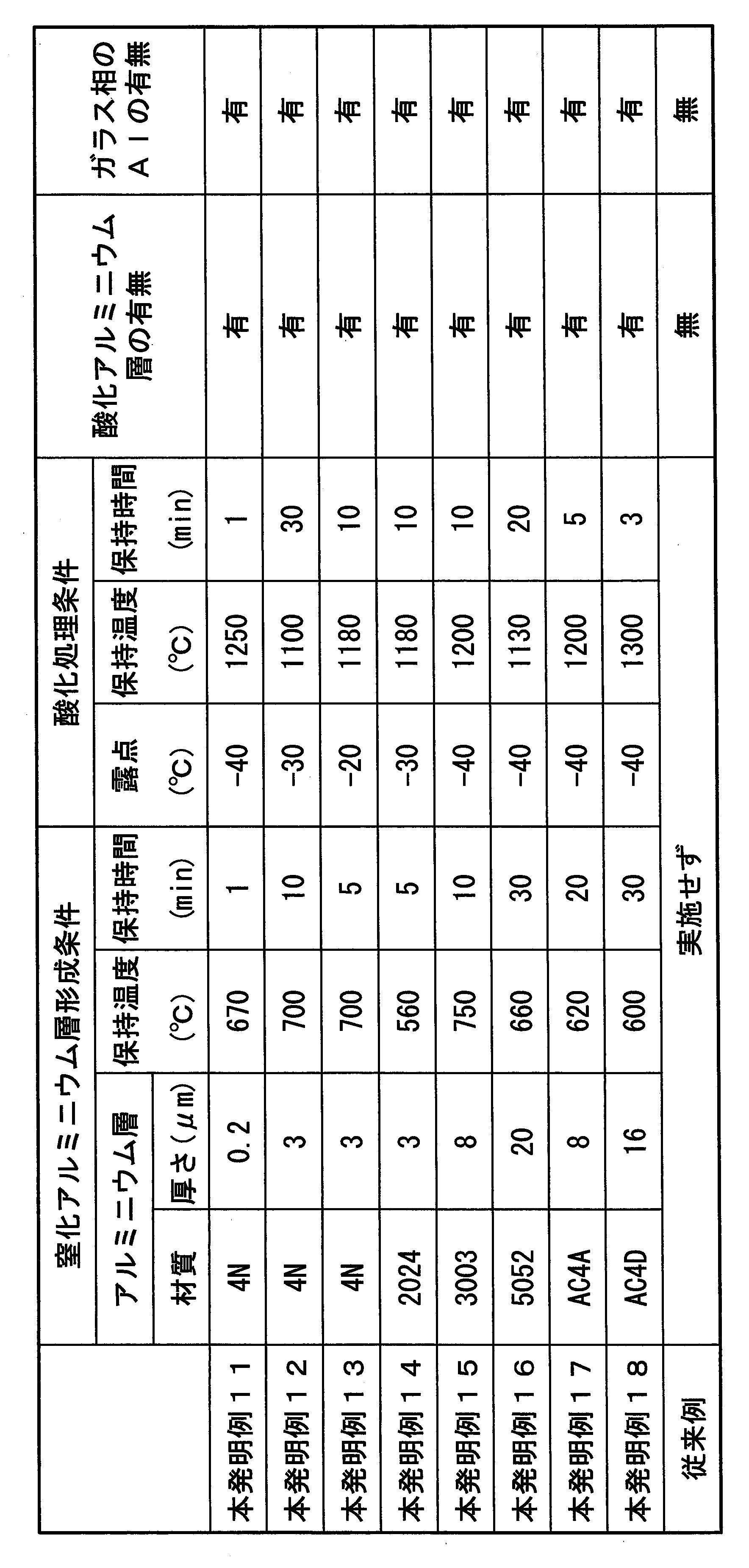

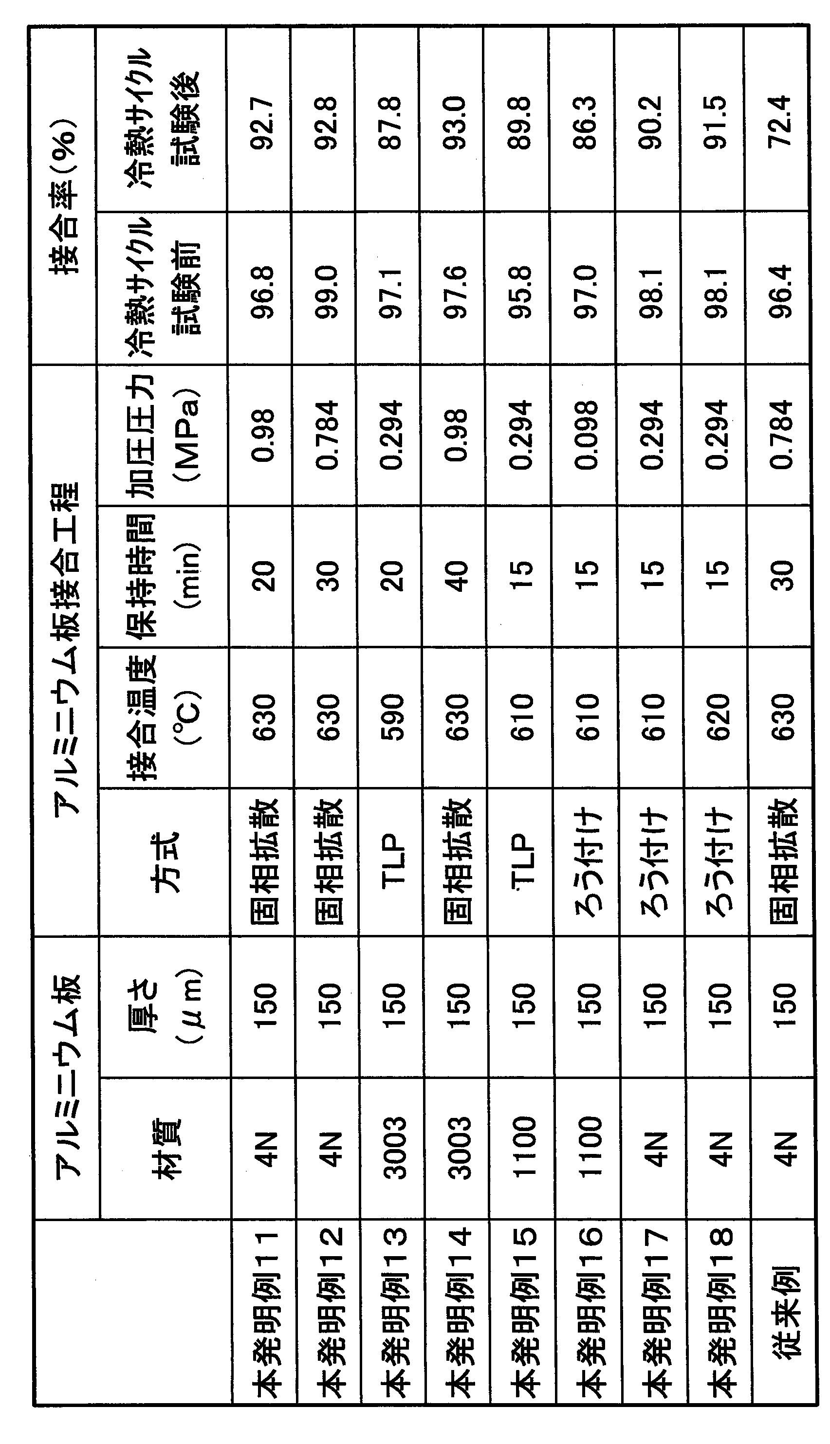
窒化ケイ素から成るセラミックス板のアルミニウム板との接合面に窒化アルミニウム層又は酸化アルミニウム層を形成しなかった従来例においては、冷熱サイクル後に接合率が大きく低下した。
これに対して、セラミックス板のアルミニウム板との接合面に窒化アルミニウム層を形成し、セラミックス板のガラス相にAlが存在する本発明例1-9、及び、セラミックス板のアルミニウム板との接合面に酸化アルミニウム層を形成し、セラミックス板のガラス相にAlが存在する本発明例11-19においては、冷熱サイクル前後での接合率の変化が小さかった。 In the conventional example in which the aluminum nitride layer or the aluminum oxide layer was not formed on the bonding surface of the ceramic plate made of silicon nitride to the aluminum plate, the bonding rate was greatly reduced after the cooling and heating cycle.
On the other hand, Example 1-9 of the present invention in which an aluminum nitride layer is formed on the bonding surface of the ceramic plate to the aluminum plate and Al is present in the glass phase of the ceramic plate, and the bonding surface of the ceramic plate to the aluminum plate In Example 11-19 of the present invention in which an aluminum oxide layer was formed on the ceramic plate and Al was present in the glass phase of the ceramic plate, the change in the bonding rate before and after the cooling / heating cycle was small.
また、本発明例1~9、11~19に示すように、アルミニウム板の接合方式によらず、ろう付け、固相拡散接合、TLPのいずれの接合方式においても、接合体の冷熱サイクル後の接合信頼性が向上することが確認された。
さらに、本発明例1~9、11~19に示すように、アルミニウム層及びアルミニウム板の組成によらず、純アルミニウム及び各種アルミニウム合金であっても、接合体の冷熱サイクル後の接合信頼性が向上することが確認された。
また、表1及び表3に示すように、窒化アルミニウム層の面積率が高くなるに従い、冷熱サイクル負荷時の接合信頼性が向上することが確認された。 Further, as shown in Examples 1 to 9 and 11 to 19 of the present invention, regardless of the joining method of the aluminum plate, in any of the joining methods of brazing, solid phase diffusion bonding, and TLP, It was confirmed that the bonding reliability was improved.
Further, as shown in Invention Examples 1 to 9 and 11 to 19, regardless of the composition of the aluminum layer and the aluminum plate, even if pure aluminum and various aluminum alloys are used, the bonding reliability of the bonded body after the thermal cycle is high. It was confirmed to improve.
Further, as shown in Tables 1 and 3, it was confirmed that as the area ratio of the aluminum nitride layer was increased, the bonding reliability under a thermal cycle load was improved.
(実施例2)
次に、窒化ケイ素から成るセラミックス板(40mm×40mm×0.32mmt)を準備し、上述した実施形態に記載された方法で、セラミックス板に窒化アルミニウム層を形成した。実施例21~24では、表5に示す条件で窒化アルミニウム層を形成した。
なお、比較例では、セラミックス板の表面に、スパッタによって窒化アルミニウム層を成膜した。
そして、得られたセラミックス基板に対して、純度99.99質量%以上(4N)のアルミニウム板(厚さ20μm)を、Al-Si系ろう材(Si:5mass%、厚さ7μm)を用いて、接合温度620℃、保持時間30min、加圧圧力0.098MPaの条件で接合し、アルミニウム/セラミックス接合体(絶縁回路基板)を製造した。 (Example 2)
Next, a ceramic plate (40 mm × 40 mm × 0.32 mmt) made of silicon nitride was prepared, and an aluminum nitride layer was formed on the ceramic plate by the method described in the above-described embodiment. In Examples 21 to 24, an aluminum nitride layer was formed under the conditions shown in Table 5.
In the comparative example, an aluminum nitride layer was formed on the surface of the ceramic plate by sputtering.
Then, with respect to the obtained ceramic substrate, an aluminum plate (thickness 20 μm) having a purity of 99.99% by mass or more (4N) is used with an Al—Si brazing material (Si: 5 mass%, thickness 7 μm). Bonding was performed under the conditions of a bonding temperature of 620 ° C., a holding time of 30 min, and a pressurizing pressure of 0.098 MPa to produce an aluminum / ceramic bonded body (insulated circuit board).
上述のようにして得られたアルミニウム/セラミックス接合体(絶縁回路基板)について、実施例1と同様に、窒化アルミニウム層、ガラス相中のAlの有無、窒化アルミニウム層の面積率、冷熱サイクル負荷前後の接合率を評価した。評価結果を表5に示す。
About the aluminum / ceramic bonding body (insulated circuit board) obtained as described above, as in Example 1, the presence / absence of Al in the aluminum nitride layer, the glass phase, the area ratio of the aluminum nitride layer, and before and after the thermal cycle load The joining rate was evaluated. The evaluation results are shown in Table 5.
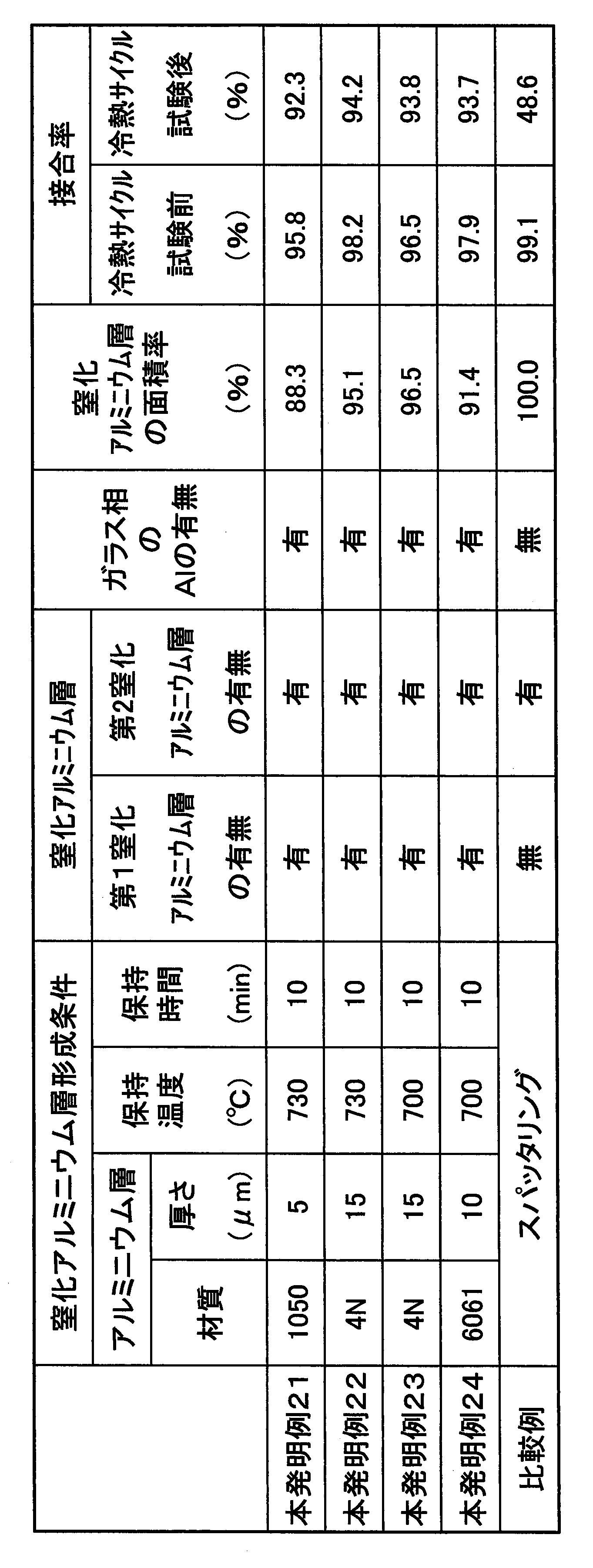
窒化ケイ素から成るセラミックス板の表面にスパッタリングによって窒化アルミニウム層を成膜した比較例においては、窒素濃度が50原子%以上80原子%以下とされ、厚さ方向に窒素の濃度傾斜を有する第1窒化アルミニウム層が形成されていなかった。また、セラミックス本体のガラス相にはAlが確認されなかった。そして、冷熱サイクル負荷後の接合率が大きく低下した。
In a comparative example in which an aluminum nitride layer is formed by sputtering on the surface of a ceramic plate made of silicon nitride, the first nitridation having a nitrogen concentration of 50 atomic% to 80 atomic% and a nitrogen concentration gradient in the thickness direction. An aluminum layer was not formed. Further, Al was not confirmed in the glass phase of the ceramic body. And the joining rate after a cold-heat cycle load fell significantly.
これに対して、窒化アルミニウム層が、窒素濃度が50原子%以上80原子%以下とされ、厚さ方向に窒素の濃度傾斜を有する第1窒化アルミニウム層と、窒素濃度が30原子%以上50原子%未満とされた第2窒化アルミニウム層と、を有している本発明例21-24においては、冷熱サイクル前後での接合率の変化が小さかった。
On the other hand, the aluminum nitride layer has a nitrogen concentration of 50 atomic percent or more and 80 atomic percent or less, and a first aluminum nitride layer having a nitrogen concentration gradient in the thickness direction, and a nitrogen concentration of 30 atomic percent or more and 50 atoms. In the inventive examples 21-24 having the second aluminum nitride layer of less than%, the change in the bonding rate before and after the cooling cycle was small.
以上のことから、本発明例によれば、窒化ケイ素(Si3N4)からなるセラミックス部材の接合面に、窒化アルミニウム層又は酸化アルミニウム層を形成することにより、アルミニウム部材が溶融することなく、セラミックス部材とアルミニウム部材とを信頼性高く接合されたセラミックス/アルミニウム接合体を提供できることが確認された。
From the above, according to the example of the present invention, by forming the aluminum nitride layer or the aluminum oxide layer on the bonding surface of the ceramic member made of silicon nitride (Si 3 N 4 ), the aluminum member does not melt, It was confirmed that a ceramic / aluminum bonded body in which a ceramic member and an aluminum member are bonded with high reliability can be provided.
本発明によれば、アルミニウム部材が溶融することなく窒化ケイ素(Si3N4)からなるセラミックス部材と信頼性高く接合されたセラミックス/アルミニウム接合体を提供することができる。
According to the present invention, it is possible to provide a ceramic / aluminum bonded body that is reliably bonded to a ceramic member made of silicon nitride (Si 3 N 4 ) without melting the aluminum member.
1、101 LEDモジュール
10、110 絶縁回路基板(セラミックス/アルミニウム接合体)
12、112 回路層(アルミニウム板,アルミニウム部材)
13 金属層(アルミニウム板,アルミニウム部材)
30、130 セラミックス基板(セラミックス部材)
31、131 セラミックス本体
32、132 窒化ケイ素相
33、133 ガラス相
36 窒化アルミニウム層
36A 第1窒化アルミニウム層
36B 第2窒化アルミニウム層
38 金属アルミニウム部
136 酸化アルミニウム層 1, 101 LED module 10, 110 Insulated circuit board (ceramic / aluminum joint)
12, 112 Circuit layer (aluminum plate, aluminum member)
13 Metal layer (aluminum plate, aluminum member)
30, 130 Ceramic substrate (ceramic member)
31, 131 Ceramic body 32, 132 Silicon nitride phase 33, 133 Glass phase 36 Aluminum nitride layer 36A First aluminum nitride layer 36B Second aluminum nitride layer 38 Metal aluminum portion 136 Aluminum oxide layer
10、110 絶縁回路基板(セラミックス/アルミニウム接合体)
12、112 回路層(アルミニウム板,アルミニウム部材)
13 金属層(アルミニウム板,アルミニウム部材)
30、130 セラミックス基板(セラミックス部材)
31、131 セラミックス本体
32、132 窒化ケイ素相
33、133 ガラス相
36 窒化アルミニウム層
36A 第1窒化アルミニウム層
36B 第2窒化アルミニウム層
38 金属アルミニウム部
136 酸化アルミニウム層 1, 101
12, 112 Circuit layer (aluminum plate, aluminum member)
13 Metal layer (aluminum plate, aluminum member)
30, 130 Ceramic substrate (ceramic member)
31, 131
Claims (12)
- セラミックス部材と、アルミニウム又はアルミニウム合金からなるアルミニウム部材とが接合されてなるセラミックス/アルミニウム接合体であって、
前記セラミックス部材は、窒化ケイ素からなるセラミックス本体と、このセラミックス本体のうち前記アルミニウム部材との接合面に形成された窒化アルミニウム層又は酸化アルミニウム層と、を有し、前記窒化アルミニウム層又は前記酸化アルミニウム層を介して前記アルミニウム部材が接合されており、
前記セラミックス本体は、窒化ケイ素相と、この窒化ケイ素相の間に形成されたガラス相と、を備えており、
前記セラミックス本体の前記ガラス相のうち前記窒化アルミニウム層又は前記酸化アルミニウム層との界面側部分にAlが存在していることを特徴とするセラミックス/アルミニウム接合体。 A ceramic / aluminum joined body in which a ceramic member and an aluminum member made of aluminum or an aluminum alloy are joined,
The ceramic member has a ceramic body made of silicon nitride, and an aluminum nitride layer or an aluminum oxide layer formed on a bonding surface of the ceramic body with the aluminum member, and the aluminum nitride layer or the aluminum oxide layer The aluminum member is bonded through a layer;
The ceramic body includes a silicon nitride phase and a glass phase formed between the silicon nitride phases,
A ceramic / aluminum bonded body, wherein Al is present in an interface side portion with the aluminum nitride layer or the aluminum oxide layer in the glass phase of the ceramic body. - 前記セラミックス本体のうち前記アルミニウム部材との接合面に前記窒化アルミニウム層が形成されており、前記窒化アルミニウム層は、前記セラミックス本体側から順に、窒素濃度が50原子%以上80原子%以下とされ、厚さ方向に窒素の濃度傾斜を有する第1窒化アルミニウム層と、窒素濃度が30原子%以上50原子%未満とされた第2窒化アルミニウム層と、を有していることを特徴とする請求項1に記載のセラミックス/アルミニウム接合体。 The aluminum nitride layer is formed on the bonding surface of the ceramic body with the aluminum member, and the aluminum nitride layer has a nitrogen concentration of 50 atomic% to 80 atomic% in order from the ceramic body side, The first aluminum nitride layer having a nitrogen concentration gradient in the thickness direction, and the second aluminum nitride layer having a nitrogen concentration of 30 atomic% or more and less than 50 atomic%. 2. The ceramic / aluminum bonded body according to 1.
- セラミックス基板と、アルミニウム又はアルミニウム合金からなるアルミニウム板とが接合されてなる絶縁回路基板であって、
前記セラミックス基板は、窒化ケイ素からなるセラミックス本体と、このセラミックス本体のうち前記アルミニウム板との接合面に形成された窒化アルミニウム層又は酸化アルミニウム層と、を有し、前記窒化アルミニウム層又は前記酸化アルミニウム層を介して前記アルミニウム板が接合されており、
前記セラミックス本体は、窒化ケイ素相と、この窒化ケイ素相の間に形成されたガラス相と、を備えており、
前記セラミックス本体の前記ガラス相のうち前記窒化アルミニウム層又は前記酸化アルミニウム層との界面側部分にAlが存在していることを特徴とする絶縁回路基板。 An insulated circuit board formed by bonding a ceramic substrate and an aluminum plate made of aluminum or an aluminum alloy,
The ceramic substrate includes a ceramic body made of silicon nitride, and an aluminum nitride layer or an aluminum oxide layer formed on a bonding surface of the ceramic body with the aluminum plate, and the aluminum nitride layer or the aluminum oxide The aluminum plate is bonded through a layer,
The ceramic body includes a silicon nitride phase and a glass phase formed between the silicon nitride phases,
An insulating circuit board, wherein Al is present in an interface side portion with the aluminum nitride layer or the aluminum oxide layer in the glass phase of the ceramic body. - 前記セラミックス本体のうち前記アルミニウム板との接合面に前記窒化アルミニウム層が形成されており、前記窒化アルミニウム層は、前記セラミックス本体側から順に、窒素濃度が50原子%以上80原子%以下とされ、厚さ方向に窒素の濃度傾斜を有する第1窒化アルミニウム層と、窒素濃度が30原子%以上50原子%未満とされた第2窒化アルミニウム層と、を有していることを特徴とする請求項3に記載の絶縁回路基板。 The aluminum nitride layer is formed on the bonding surface of the ceramic body with the aluminum plate, and the aluminum nitride layer has a nitrogen concentration of 50 atomic% to 80 atomic% in order from the ceramic body side, The first aluminum nitride layer having a nitrogen concentration gradient in the thickness direction, and the second aluminum nitride layer having a nitrogen concentration of 30 atomic% or more and less than 50 atomic%. 3. The insulated circuit board according to 3.
- 請求項3又は請求項4に記載の絶縁回路基板と、前記アルミニウム板の前記セラミックス基板とは反対側の面に接合されたLED素子と、を備えていることを特徴とするLEDモジュール。 5. An LED module comprising: the insulated circuit board according to claim 3 or 4; and an LED element bonded to a surface of the aluminum plate opposite to the ceramic substrate.
- 窒化ケイ素からなるセラミックス本体と、このセラミックス本体の表面に形成された窒化アルミニウム層又は酸化アルミニウム層と、を備え、
前記セラミックス本体は、窒化ケイ素相と、この窒化ケイ素相の間に形成されたガラス相と、を備えており、
前記セラミックス本体の前記ガラス相のうち前記窒化アルミニウム層又は前記酸化アルミニウム層との界面側部分にAlが存在していることを特徴とするセラミックス部材。 A ceramic body made of silicon nitride, and an aluminum nitride layer or an aluminum oxide layer formed on the surface of the ceramic body,
The ceramic body includes a silicon nitride phase and a glass phase formed between the silicon nitride phases,
A ceramic member, wherein Al is present in an interface side portion with the aluminum nitride layer or the aluminum oxide layer in the glass phase of the ceramic body. - 前記セラミックス本体の表面に前記窒化アルミニウム層が形成されており、前記窒化アルミニウム層は、前記セラミックス本体側から順に、窒素濃度が50原子%以上80原子%以下とされ、厚さ方向に窒素の濃度傾斜を有する第1窒化アルミニウム層と、窒素濃度が30原子%以上50原子%未満とされた第2窒化アルミニウム層と、を有していることを特徴とする請求項6に記載のセラミックス部材。 The aluminum nitride layer is formed on the surface of the ceramic body, and the aluminum nitride layer has a nitrogen concentration of 50 atomic% or more and 80 atomic% or less in order from the ceramic body side, and the concentration of nitrogen in the thickness direction. The ceramic member according to claim 6, comprising a first aluminum nitride layer having an inclination and a second aluminum nitride layer having a nitrogen concentration of 30 atomic% or more and less than 50 atomic%.
- 前記セラミックス本体の表面に前記窒化アルミニウム層が形成されており、この窒化アルミニウム層のうち前記セラミックス本体とは反対側の面に、金属アルミニウム部が形成されていることを特徴とする請求項6又は請求項7に記載のセラミックス部材。 The aluminum nitride layer is formed on a surface of the ceramic body, and a metal aluminum portion is formed on a surface of the aluminum nitride layer opposite to the ceramic body. The ceramic member according to claim 7.
- 請求項1又は請求項2に記載のセラミックス/アルミニウム接合体を製造するセラミックス/アルミニウム接合体の製造方法であって、
窒化ケイ素からなるセラミックス本体の表面に、厚さ20μm以下のアルミニウム層を形成するアルミニウム層形成工程と、
前記アルミニウム層が形成されたセラミックス本体を、前記アルミニウム層の固相線温度以上の温度まで加熱し、窒化アルミニウム層を形成する窒化アルミニウム層形成工程と、
前記窒化アルミニウム層を介してアルミニウム部材を接合するアルミニウム部材接合工程と、
を備えていることを特徴とするセラミックス/アルミニウム接合体の製造方法。 A method for producing a ceramic / aluminum joined body for producing the ceramic / aluminum joined body according to claim 1 or 2,
An aluminum layer forming step of forming an aluminum layer having a thickness of 20 μm or less on the surface of the ceramic body made of silicon nitride;
Heating the ceramic body on which the aluminum layer has been formed to a temperature equal to or higher than the solidus temperature of the aluminum layer to form an aluminum nitride layer; and
An aluminum member bonding step of bonding an aluminum member through the aluminum nitride layer;
A method for producing a ceramic / aluminum joined body comprising: - 前記窒化アルミニウム層を酸化させて酸化アルミニウム層を形成する酸化処理工程と、前記酸化アルミニウム層を介してアルミニウム部材を接合するアルミニウム部材接合工程と、を備えていることを特徴とする請求項9に記載のセラミックス/アルミニウム接合体の製造方法。 10. The method according to claim 9, further comprising: an oxidation treatment step of oxidizing the aluminum nitride layer to form an aluminum oxide layer; and an aluminum member bonding step of bonding an aluminum member via the aluminum oxide layer. A method for producing the ceramic / aluminum bonded body according to the description.
- 請求項3又は請求項4に記載の絶縁回路基板を製造する絶縁回路基板の製造方法であって、
窒化ケイ素からなるセラミックス本体の表面に、厚さ20μm以下のアルミニウム層を形成するアルミニウム層形成工程と、
前記アルミニウム層が形成されたセラミックス本体を、前記アルミニウム層の固相線温度以上の温度まで加熱し、窒化アルミニウム層を形成する窒化アルミニウム層形成工程と、
前記窒化アルミニウム層を介してアルミニウム板を接合するアルミニウム板接合工程と、
を備えていることを特徴とする絶縁回路基板の製造方法。 A method for producing an insulated circuit board for producing an insulated circuit board according to claim 3 or 4,
An aluminum layer forming step of forming an aluminum layer having a thickness of 20 μm or less on the surface of the ceramic body made of silicon nitride;
Heating the ceramic body on which the aluminum layer has been formed to a temperature equal to or higher than the solidus temperature of the aluminum layer to form an aluminum nitride layer; and
An aluminum plate joining step for joining an aluminum plate via the aluminum nitride layer;
A method for producing an insulated circuit board, comprising: - 前記窒化アルミニウム層を酸化させて酸化アルミニウム層を形成する酸化処理工程と、前記酸化アルミニウム層を介してアルミニウム板を接合するアルミニウム板接合工程と、を備えていることを特徴とする請求項11に記載の絶縁回路基板の製造方法。 12. The method according to claim 11, further comprising: an oxidation treatment step of oxidizing the aluminum nitride layer to form an aluminum oxide layer, and an aluminum plate joining step of joining an aluminum plate via the aluminum oxide layer. The manufacturing method of the insulated circuit board of description.
Priority Applications (4)
| Application Number | Priority Date | Filing Date | Title |
|---|---|---|---|
| US16/482,018 US11798856B2 (en) | 2017-02-06 | 2018-02-06 | Ceramic/aluminum bonded body, insulating substrate, LED module, ceramic member, method for producing ceramic/aluminum bonded body, and method for producing insulating substrate |
| CN201880007306.6A CN110191869B (en) | 2017-02-06 | 2018-02-06 | Ceramic-aluminum junction body, method for producing ceramic-aluminum junction body, insulated circuit board, method for producing insulated circuit board, LED module, and ceramic member |
| KR1020197016412A KR102466817B1 (en) | 2017-02-06 | 2018-02-06 | Ceramics/aluminum junction, insulated circuit board, LED module, ceramic member, method for manufacturing ceramics/aluminum junction, method for manufacturing insulated circuit board |
| EP18747966.2A EP3578535A4 (en) | 2017-02-06 | 2018-02-06 | Ceramic/aluminum conjugate, insulated circuit board, led module, ceramic member, method for producing ceramic/aluminum conjugate, and method for producing insulated circuit board |
Applications Claiming Priority (4)
| Application Number | Priority Date | Filing Date | Title |
|---|---|---|---|
| JP2017-019737 | 2017-02-06 | ||
| JP2017019737 | 2017-02-06 | ||
| JP2018009821A JP7052374B2 (en) | 2017-02-06 | 2018-01-24 | Manufacturing method of ceramics / aluminum joint, manufacturing method of insulated circuit board |
| JP2018-009821 | 2018-01-24 |
Publications (1)
| Publication Number | Publication Date |
|---|---|
| WO2018143470A1 true WO2018143470A1 (en) | 2018-08-09 |
Family
ID=63039893
Family Applications (1)
| Application Number | Title | Priority Date | Filing Date |
|---|---|---|---|
| PCT/JP2018/003957 WO2018143470A1 (en) | 2017-02-06 | 2018-02-06 | Ceramic/aluminum conjugate, insulated circuit board, led module, ceramic member, method for producing ceramic/aluminum conjugate, and method for producing insulated circuit board |
Country Status (3)
| Country | Link |
|---|---|
| JP (1) | JP7243793B2 (en) |
| TW (1) | TWI744474B (en) |
| WO (1) | WO2018143470A1 (en) |
Cited By (1)
| Publication number | Priority date | Publication date | Assignee | Title |
|---|---|---|---|---|
| CN113454772A (en) * | 2019-02-22 | 2021-09-28 | 同和金属技术有限公司 | Metal-ceramic bonded substrate and method for producing same |
Families Citing this family (1)
| Publication number | Priority date | Publication date | Assignee | Title |
|---|---|---|---|---|
| WO2020261833A1 (en) * | 2019-06-26 | 2020-12-30 | 三菱マテリアル株式会社 | Copper/ceramic joined body, insulation circuit board, copper/ceramic joined body production method, and insulation circuit board manufacturing method |
Citations (9)
| Publication number | Priority date | Publication date | Assignee | Title |
|---|---|---|---|---|
| JPH09153567A (en) * | 1995-09-28 | 1997-06-10 | Toshiba Corp | Heat conductive silicon nitride circuit board and semiconductor device |
| JPH11154719A (en) * | 1997-03-14 | 1999-06-08 | Toshiba Corp | Silicon nitride circuit board, manufacture of semiconductor device and the circuit board |
| JP3171234B2 (en) | 1997-03-26 | 2001-05-28 | 三菱マテリアル株式会社 | Ceramic circuit board with heat sink |
| JP2010010563A (en) * | 2008-06-30 | 2010-01-14 | Mitsubishi Materials Corp | Method for manufacturing power module substrate and power module substrate |
| WO2011004798A1 (en) * | 2009-07-06 | 2011-01-13 | 株式会社 東芝 | Element mounting ceramic substrate, led mounting ceramic substrate, led lamp, and head light, and electronic component |
| JP2013153157A (en) | 2011-12-28 | 2013-08-08 | Nichia Chem Ind Ltd | Package molding for light emitting device |
| JP2015070199A (en) | 2013-09-30 | 2015-04-13 | 日亜化学工業株式会社 | Light-emitting device |
| JP2017019737A (en) | 2015-07-09 | 2017-01-26 | 学校法人日本大学 | Inhibitor for cell death due to endoplasmic reticulum stress, endoplasmic reticulum stress control agent, and preventive/therapeutic agent comprising the control agent as active ingredient |
| JP2018009821A (en) | 2016-07-12 | 2018-01-18 | 飛島建設株式会社 | Concrete demold time strength estimation system |
Family Cites Families (5)
| Publication number | Priority date | Publication date | Assignee | Title |
|---|---|---|---|---|
| JPS60171277A (en) * | 1984-02-17 | 1985-09-04 | 株式会社東芝 | Metal-ceramic bonded body |
| JP4649027B2 (en) * | 1999-09-28 | 2011-03-09 | 株式会社東芝 | Ceramic circuit board |
| JP5038565B2 (en) | 2000-09-22 | 2012-10-03 | 株式会社東芝 | Ceramic circuit board and manufacturing method thereof |
| JP5122098B2 (en) | 2006-08-11 | 2013-01-16 | 株式会社トクヤマ | Metallized substrate, semiconductor device |
| JP2008063187A (en) | 2006-09-07 | 2008-03-21 | Ngk Spark Plug Co Ltd | Silicon nitride sintered compact, ceramic substrate for heat dissipation and insulation, circuit board for heat dissipation and insulation and module for heat dissipation and insulation |
-
2018
- 2018-02-06 WO PCT/JP2018/003957 patent/WO2018143470A1/en active Application Filing
- 2018-02-06 TW TW107104124A patent/TWI744474B/en active
-
2021
- 2021-11-01 JP JP2021178764A patent/JP7243793B2/en active Active
Patent Citations (9)
| Publication number | Priority date | Publication date | Assignee | Title |
|---|---|---|---|---|
| JPH09153567A (en) * | 1995-09-28 | 1997-06-10 | Toshiba Corp | Heat conductive silicon nitride circuit board and semiconductor device |
| JPH11154719A (en) * | 1997-03-14 | 1999-06-08 | Toshiba Corp | Silicon nitride circuit board, manufacture of semiconductor device and the circuit board |
| JP3171234B2 (en) | 1997-03-26 | 2001-05-28 | 三菱マテリアル株式会社 | Ceramic circuit board with heat sink |
| JP2010010563A (en) * | 2008-06-30 | 2010-01-14 | Mitsubishi Materials Corp | Method for manufacturing power module substrate and power module substrate |
| WO2011004798A1 (en) * | 2009-07-06 | 2011-01-13 | 株式会社 東芝 | Element mounting ceramic substrate, led mounting ceramic substrate, led lamp, and head light, and electronic component |
| JP2013153157A (en) | 2011-12-28 | 2013-08-08 | Nichia Chem Ind Ltd | Package molding for light emitting device |
| JP2015070199A (en) | 2013-09-30 | 2015-04-13 | 日亜化学工業株式会社 | Light-emitting device |
| JP2017019737A (en) | 2015-07-09 | 2017-01-26 | 学校法人日本大学 | Inhibitor for cell death due to endoplasmic reticulum stress, endoplasmic reticulum stress control agent, and preventive/therapeutic agent comprising the control agent as active ingredient |
| JP2018009821A (en) | 2016-07-12 | 2018-01-18 | 飛島建設株式会社 | Concrete demold time strength estimation system |
Cited By (1)
| Publication number | Priority date | Publication date | Assignee | Title |
|---|---|---|---|---|
| CN113454772A (en) * | 2019-02-22 | 2021-09-28 | 同和金属技术有限公司 | Metal-ceramic bonded substrate and method for producing same |
Also Published As
| Publication number | Publication date |
|---|---|
| TWI744474B (en) | 2021-11-01 |
| JP7243793B2 (en) | 2023-03-22 |
| TW201841870A (en) | 2018-12-01 |
| JP2022023954A (en) | 2022-02-08 |
Similar Documents
| Publication | Publication Date | Title |
|---|---|---|
| WO2015046280A1 (en) | Cu/ceramic material joint, method for manufacturing cu/ceramic material joint, and substrate for power module | |
| CN112601729B (en) | Copper-ceramic joined body, insulated circuit board, method for producing copper-ceramic joined body, and method for producing insulated circuit board | |
| JP7243793B2 (en) | Ceramic/aluminum joints, insulated circuit boards, LED modules, ceramic members | |
| JP2017183716A (en) | Manufacturing method of insulation circuit board with heat sink, and insulation circuit board with heat sink | |
| WO2021033421A1 (en) | Copper/ceramic assembly, insulated circuit board, method for producing copper/ceramic assembly, and method for producing insulated circuit board | |
| JP7052374B2 (en) | Manufacturing method of ceramics / aluminum joint, manufacturing method of insulated circuit board | |
| JP6569511B2 (en) | Bonded body, power module substrate with cooler, and method for manufacturing power module substrate with cooler | |
| WO2020044590A1 (en) | Copper/ceramic bonded body, insulation circuit board, method for producing copper/ceramic bonded body, and method for manufacturing insulation circuit board | |
| JP6750422B2 (en) | Method for manufacturing insulated circuit board, insulated circuit board, power module, LED module, and thermoelectric module | |
| EP4071128B1 (en) | Copper/ceramic bonded body, insulating circuit board, method for producing copper/ceramic bonded body, and method for producing insulating circuit board | |
| JP2016143830A (en) | Substrate for power module with heat sink, power module, and method of manufacturing substrate for power module with heat sink | |
| JP6561886B2 (en) | Manufacturing method of power module substrate with heat sink | |
| JP2015177045A (en) | Copper/ceramic assembly and power module substrate | |
| WO2020044594A1 (en) | Copper/ceramic bonded body, insulation circuit board, method for producing copper/ceramic bonded body, and method for manufacturing insulation circuit board | |
| JP2018046106A (en) | Copper/titanium/aluminum conjugate, insulation circuit board, insulation circuit board with heat sink, power module, led module, and electro-thermal module | |
| JP7424043B2 (en) | Copper/ceramic bonded body, insulated circuit board, method for manufacturing copper/ceramic bonded body, method for manufacturing insulated circuit board | |
| WO2023286858A1 (en) | Copper/ceramic assembly, insulating circuit substrate, production method for copper/ceramic assembly, and production method for insulating circuit substrate | |
| JP2018167275A (en) | Manufacturing method for conjugant, manufacturing method for insulation circuit board, conjugant, and insulation circuit board | |
| JP2020096054A (en) | Manufacturing method of conjugant, manufacturing method of insulative circuit board, ceramic board, conjugant, and insulative circuit board | |
| WO2019159219A1 (en) | Copper/titanium/aluminum joint, insulating circuit board, insulating circuit board with heat sink, power module, led module, and thermoelectric module | |
| JP2017168730A (en) | Circuit board and its manufacturing method | |
| JP2021091596A (en) | Copper/ceramic assembly, insulation circuit board, method for manufacturing copper/ceramic assembly, and method for manufacturing insulation circuit board | |
| JP2019165100A (en) | Method for manufacturing substrate for heat sink-equipped power module | |
| JP2022165044A (en) | Copper/ceramic assembly and insulation circuit board | |
| JP2017157677A (en) | Method for manufacturing assembly, method for manufacturing substrate for power module, and method for manufacturing substrate for heat sink-equipped power module |
Legal Events
| Date | Code | Title | Description |
|---|---|---|---|
| 121 | Ep: the epo has been informed by wipo that ep was designated in this application |
Ref document number: 18747966 Country of ref document: EP Kind code of ref document: A1 |
|
| ENP | Entry into the national phase |
Ref document number: 20197016412 Country of ref document: KR Kind code of ref document: A |
|
| NENP | Non-entry into the national phase |
Ref country code: DE |
|
| WWE | Wipo information: entry into national phase |
Ref document number: 2018747966 Country of ref document: EP |