WO2018143368A1 - 半導体デバイス - Google Patents
半導体デバイス Download PDFInfo
- Publication number
- WO2018143368A1 WO2018143368A1 PCT/JP2018/003475 JP2018003475W WO2018143368A1 WO 2018143368 A1 WO2018143368 A1 WO 2018143368A1 JP 2018003475 W JP2018003475 W JP 2018003475W WO 2018143368 A1 WO2018143368 A1 WO 2018143368A1
- Authority
- WO
- WIPO (PCT)
- Prior art keywords
- layer
- electrode layer
- semiconductor device
- elastic
- thickness
- Prior art date
- Legal status (The legal status is an assumption and is not a legal conclusion. Google has not performed a legal analysis and makes no representation as to the accuracy of the status listed.)
- Ceased
Links
Images


Classifications
-
- H—ELECTRICITY
- H10—SEMICONDUCTOR DEVICES; ELECTRIC SOLID-STATE DEVICES NOT OTHERWISE PROVIDED FOR
- H10F—INORGANIC SEMICONDUCTOR DEVICES SENSITIVE TO INFRARED RADIATION, LIGHT, ELECTROMAGNETIC RADIATION OF SHORTER WAVELENGTH OR CORPUSCULAR RADIATION
- H10F77/00—Constructional details of devices covered by this subclass
- H10F77/20—Electrodes
- H10F77/206—Electrodes for devices having potential barriers
- H10F77/211—Electrodes for devices having potential barriers for photovoltaic cells
-
- H—ELECTRICITY
- H10—SEMICONDUCTOR DEVICES; ELECTRIC SOLID-STATE DEVICES NOT OTHERWISE PROVIDED FOR
- H10F—INORGANIC SEMICONDUCTOR DEVICES SENSITIVE TO INFRARED RADIATION, LIGHT, ELECTROMAGNETIC RADIATION OF SHORTER WAVELENGTH OR CORPUSCULAR RADIATION
- H10F19/00—Integrated devices, or assemblies of multiple devices, comprising at least one photovoltaic cell covered by group H10F10/00, e.g. photovoltaic modules
- H10F19/30—Integrated devices, or assemblies of multiple devices, comprising at least one photovoltaic cell covered by group H10F10/00, e.g. photovoltaic modules comprising thin-film photovoltaic cells
-
- H—ELECTRICITY
- H10—SEMICONDUCTOR DEVICES; ELECTRIC SOLID-STATE DEVICES NOT OTHERWISE PROVIDED FOR
- H10F—INORGANIC SEMICONDUCTOR DEVICES SENSITIVE TO INFRARED RADIATION, LIGHT, ELECTROMAGNETIC RADIATION OF SHORTER WAVELENGTH OR CORPUSCULAR RADIATION
- H10F19/00—Integrated devices, or assemblies of multiple devices, comprising at least one photovoltaic cell covered by group H10F10/00, e.g. photovoltaic modules
- H10F19/80—Encapsulations or containers for integrated devices, or assemblies of multiple devices, having photovoltaic cells
- H10F19/804—Materials of encapsulations
-
- H—ELECTRICITY
- H10—SEMICONDUCTOR DEVICES; ELECTRIC SOLID-STATE DEVICES NOT OTHERWISE PROVIDED FOR
- H10F—INORGANIC SEMICONDUCTOR DEVICES SENSITIVE TO INFRARED RADIATION, LIGHT, ELECTROMAGNETIC RADIATION OF SHORTER WAVELENGTH OR CORPUSCULAR RADIATION
- H10F71/00—Manufacture or treatment of devices covered by this subclass
- H10F71/138—Manufacture of transparent electrodes, e.g. transparent conductive oxides [TCO] or indium tin oxide [ITO] electrodes
-
- H—ELECTRICITY
- H10—SEMICONDUCTOR DEVICES; ELECTRIC SOLID-STATE DEVICES NOT OTHERWISE PROVIDED FOR
- H10F—INORGANIC SEMICONDUCTOR DEVICES SENSITIVE TO INFRARED RADIATION, LIGHT, ELECTROMAGNETIC RADIATION OF SHORTER WAVELENGTH OR CORPUSCULAR RADIATION
- H10F77/00—Constructional details of devices covered by this subclass
- H10F77/20—Electrodes
-
- H—ELECTRICITY
- H10—SEMICONDUCTOR DEVICES; ELECTRIC SOLID-STATE DEVICES NOT OTHERWISE PROVIDED FOR
- H10K—ORGANIC ELECTRIC SOLID-STATE DEVICES
- H10K77/00—Constructional details of devices covered by this subclass and not covered by groups H10K10/80, H10K30/80, H10K50/80 or H10K59/80
- H10K77/10—Substrates, e.g. flexible substrates
- H10K77/111—Flexible substrates
-
- H—ELECTRICITY
- H10—SEMICONDUCTOR DEVICES; ELECTRIC SOLID-STATE DEVICES NOT OTHERWISE PROVIDED FOR
- H10F—INORGANIC SEMICONDUCTOR DEVICES SENSITIVE TO INFRARED RADIATION, LIGHT, ELECTROMAGNETIC RADIATION OF SHORTER WAVELENGTH OR CORPUSCULAR RADIATION
- H10F71/00—Manufacture or treatment of devices covered by this subclass
- H10F71/121—The active layers comprising only Group IV materials
- H10F71/1221—The active layers comprising only Group IV materials comprising polycrystalline silicon
-
- Y—GENERAL TAGGING OF NEW TECHNOLOGICAL DEVELOPMENTS; GENERAL TAGGING OF CROSS-SECTIONAL TECHNOLOGIES SPANNING OVER SEVERAL SECTIONS OF THE IPC; TECHNICAL SUBJECTS COVERED BY FORMER USPC CROSS-REFERENCE ART COLLECTIONS [XRACs] AND DIGESTS
- Y02—TECHNOLOGIES OR APPLICATIONS FOR MITIGATION OR ADAPTATION AGAINST CLIMATE CHANGE
- Y02E—REDUCTION OF GREENHOUSE GAS [GHG] EMISSIONS, RELATED TO ENERGY GENERATION, TRANSMISSION OR DISTRIBUTION
- Y02E10/00—Energy generation through renewable energy sources
- Y02E10/50—Photovoltaic [PV] energy
- Y02E10/549—Organic PV cells
Definitions
- the present invention relates to a semiconductor device.
- Non-Patent Document 1 Martin Kaltenbrunner, Tsuyoshi Sekitani, Jonathan Reeder, Tomoyuki Yokota, Kazunori Kuribara, Takeyoshi Tokuhara, Michael Drack, Reinhard Schwodiauer, Ingrid Graz, Simona Bauer-Gogonea, Siegfried Bauer, Takao Someya, "An ultra-lightweight design for impercept plastic electronics ", Nature, 499, (7459), 458-463, 2013.
- a flexible sheet device in which a flexible sensor, a power generation element, a light emitting element, a secondary battery, and the like are combined with such a flexible electronic circuit has been proposed.
- this type of seat device taking advantage of its lightweight and flexible features, it is a wearable device that can be worn directly on clothing or on the body surface, monitoring human and animal body temperature, pulse rate, body moisture content, blood pressure, and other health indicators. Attempts to disseminate or record data and use it for health care are drawing attention. Wearable devices are required to follow the movement of humans or animals, withstand bending during attachment / detachment, and to be usable for a certain period of time without causing deterioration in performance or the like.
- a device with a laminated structure that is less likely to cause breakage or performance deterioration during bending deformation.
- a semiconductor device provided with two electrode layers and a semiconductor layer provided between the electrode layers if the difference in strain applied to the two electrode layers when the semiconductor device is deformed is large, one electrode to which greater strain is applied The layer is extremely easy to break than the other electrode layer.
- a semiconductor device may include a first base layer having elasticity.
- the semiconductor device may include a first electrode layer provided on the first base material layer.
- the semiconductor device may include a semiconductor layer provided on the first electrode layer.
- the semiconductor device may include a second electrode layer provided on the semiconductor layer.
- the semiconductor device may include a second base layer that is provided on the second electrode layer and has elasticity. In the thickness direction of the semiconductor device, the distance b from one surface of the semiconductor device is May be located between the center of the first electrode layer and the center of the second electrode layer in the thickness direction.
- n indicates the number of layers included in the semiconductor device
- E i indicates the elastic modulus of the i-th layer from the one surface side of the semiconductor device among the layers included in the semiconductor device
- t i and t j are , Respectively indicate the thickness of the i-th layer and the thickness of the j-th layer.
- the first base material layer may include a first elastic layer.
- the first base material layer may include a first film layer provided on the first elastic body layer.
- the first electrode layer may be provided on the first film layer.
- the second base material layer may include a second film layer provided on the second electrode layer.
- the second base material layer may include a second elastic layer provided on the second film layer.
- the elastic modulus of the first elastic layer is E 1
- the thickness is t 1
- the elastic modulus of the second elastic layer is E 7
- the thickness is t 7 , 0.2 ⁇ t 7 / t 1 ⁇ 5 and 0.1 ⁇ (E 7 / E 1 ) ⁇ (t 7 / t 1 ) 2 ⁇ 10 may be satisfied.
- the modulus of elasticity of the first elastic layer E 1, the thickness t 1, E 7 the elastic modulus of the second elastic layer, the thickness is taken as t 7, 0.5 ⁇ (E 7 / E 1) ⁇ It is preferable to satisfy (t 7 / t 1 ) 2 ⁇ 2.
- the elastic modulus of the first elastic layer is E 1
- the thickness is t 1
- the elastic modulus of the second elastic layer is E 7
- the thickness is t 7 , 0.8 ⁇ (E 7 / E 1 ) ⁇ It is more preferable to satisfy (t 7 / t 1 ) 2 ⁇ 1.25.
- the thickness of the first elastic layer is t 1 and the thickness of the second elastic layer is t 7 , 0.5 ⁇ t 7 / t 1 ⁇ 2 may be satisfied.
- t 1 is the thickness of the first elastic layer and t 7 is the thickness of the second elastic layer.
- At least one of the t 1 and t 7 may be 10 ⁇ m or more.
- At least one of the t 1 and t 7 is 50 ⁇ m or more.
- At least one of the t 1 and t 7 is 100 ⁇ m or more.
- the first electrode layer may be a transparent electrode layer, and the first elastic layer may be light transmissive.
- the first electrode layer may be visible light transmissive.
- the semiconductor device has a photovoltaic power generation function or a light emission function
- the average value of the total light transmittance in the visible light band is preferably 60% or more, and more preferably 70% or more. There is no problem even if it has scattering properties in a range satisfying these.
- the semiconductor layer may be a photoelectric conversion layer, a current light emitting layer, an electroluminescent layer, an organic transistor layer, or a combination thereof. Appropriate selections and combinations are used depending on the application.
- an organic semiconductor material is preferably used from the viewpoint of flexibility and coating properties, but a compound semiconductor material such as CIGS or CIS or a perovskite type compound material can also be used depending on the purpose.
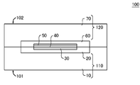
- FIG. 4 is a cross-sectional view for explaining a strain ⁇ generated in the solar cell device 100.
- FIG. 1 schematically shows an example of a cross section of a solar cell device 100 according to an embodiment.
- the solar cell device 100 is an example of a semiconductor device.
- the solar cell device 100 includes a first base layer 110, a first electrode layer 30, a photoelectric conversion layer 40, a second electrode layer 50, and a second base layer 120.
- the first electrode layer 30 is provided on the first base material layer 110.
- the second base material layer 120 is provided on the second electrode layer 50.
- the first base material layer 110 includes the first elastic layer 10 and the first film layer 20.
- the second base material layer 120 includes a second film layer 60 and a second elastic layer 70.
- the first base material layer 110 and the second base material layer 120 have elasticity.
- the 1st base material layer 110 has translucency.
- the 2nd base material layer 120 does not need to have translucency, it may have translucency.
- the first elastic layer 10 provides the first surface 101 of the solar cell device 100
- the second elastic layer 70 provides the second surface 102 of the solar cell device 100.
- the first surface 101 is an incident surface on which light is incident on the solar cell device 100.
- Each layer included in the solar cell device 100 includes, from the first surface 101 side, the first elastic layer 10, the first film layer 20, the first electrode layer 30, the photoelectric conversion layer 40, the second electrode layer 50, and the second film.
- the layer 60 and the second elastic layer 70 are provided in this order.
- the first elastic layer 10 has translucency.
- the first elastic layer 10 is made of an elastic material.
- the first elastic layer 10 may be a rubber layer formed of a rubber material such as acrylic rubber, silicon rubber, butadiene rubber, styrene butadiene rubber, isoprene rubber, chloroprene rubber, nitrile rubber, ethylene propylene rubber, and urethane rubber.
- it may be a soft fluororesin material such as ETFE or PVF.
- polyolefins such as polyethylene, polypropylene, polyvinyl chloride, polyvinylidene chloride, polyvinyl alcohol, soft polyolefin copolymers such as EVA, EMA, polystyrene, AS resin, ABS resin, foams thereof, or polycarbonate, polyamide, polyester
- resins may be cured resins such as polycondensation resins such as phenol resins, melamine resins, urea resins, epoxy resins, acrylic resins, methacrylic resins, and unsaturated polyester resins.
- the average value of the total light transmittance in the visible light band is preferably 60% or more, and 70% or more. Is more preferable. There is no problem even if it has scattering properties in a range satisfying these.
- the first film layer 20 is provided on the first elastic layer 10.
- the 1st film layer 20 has translucency.
- the first film layer 20 is formed of a resin material.
- the first film layer 20 includes a xylylene polymer material such as parylene, an epoxy resin material such as SU-8, a polyester material such as polyethylene terephthalate and polyethylene naphthalate, a cyclopolyolefin material, a polycarbonate material, and a methacrylic resin. It may be formed of a material, a polyimide material, various photoresist materials, or the like.
- a photocuring or thermosetting resin material or a transparent polyimide material is preferably used from the viewpoint of transparency, heat resistance, surface smoothness, and the like.
- it may be formed of a flexible glass substrate having a thickness of 50 ⁇ m or less, preferably 30 ⁇ m or less, and most preferably 10 ⁇ m or less.
- a substrate having a resin coating for smoothing microcracks on both sides is preferably used to prevent breakage.
- the first film layer 20 may be used as a base material for forming the first electrode layer 30 when the solar cell device 100 is manufactured.
- the first electrode layer 30 is provided on the first film layer 20.
- the first electrode layer 30 has translucency. Specifically, the first electrode layer 30 has visible light transparency.
- the average value of the total light transmittance of the first electrode layer 30 in the visible light band is preferably 60% or more, and more preferably 70% or more.
- the first electrode layer 30 may have light scattering properties in a range where the total light transmittance satisfies these values.
- the first electrode layer 30 is, for example, a transparent electrode layer.
- the first electrode layer 30 may be formed of metal oxide such as indium tin oxide (ITO), nickel oxide, tin oxide, indium oxide, indium-zirconium oxide (IZO), titanium oxide, and zinc oxide.
- it is made of a thin film of aluminum or silver, or a light-transmitting organic conductive material such as PEDOT: PSS, or a combination thereof, or a thin wire such as aluminum, gold, silver, or copper. It may be combined with an auxiliary electrode.
- a thin film of aluminum or silver or a light-transmitting organic conductive material such as PEDOT: PSS, or a combination thereof, or a thin wire such as aluminum, gold, silver, or copper. It may be combined with an auxiliary electrode.
- the first electrode layer 30 may be a metal mesh layer in which a metal having a mesh structure as an electrode is held by a translucent material.
- the mesh structure may be formed of silver, gold, copper or the like.
- the first electrode layer 30 may be a metal nanowire layer in which metal nanowires as electrodes are held with a light-transmitting material. When a metal mesh layer or a metal nanowire layer is applied as the first electrode layer 30, the electrode portion may not have a light-transmitting property, and the portion formed of the light-transmitting material transmits the first light.
- the electrode layer 30 may have translucency as a whole.
- the first electrode layer 30 may be formed of a conductive polymer.
- the photoelectric conversion layer 40 is provided on the first electrode layer 30.
- the photoelectric conversion layer 40 has a plurality of photoelectric conversion elements.
- the photoelectric conversion layer 40 may be a layer made of thin film single crystal silicon, thin film polycrystalline silicon, thin film microcrystalline silicon, amorphous silicon, a perovskite compound, other inorganic semiconductor materials, and a dye material.
- the photoelectric conversion layer 40 may be a layer made of an organic semiconductor material.
- the organic semiconductor material may be a mixed layer in which an n-type organic semiconductor and a p-type organic semiconductor are bulk heterojunctioned.
- n-type organic semiconductors include fullerenes, fullerene derivatives, carbon materials such as carbon nanotubes, various condensed aromatic hydrocarbons, perylenes, cyanoquinodimethanes, oxadiazole derivatives such as PBD, and styrylanthracenes such as BSA-1. Derivatives, bathocuproine, benzoquinolinol beryllium complex, benzothiazole zinc complex and the like.
- the p-type organic semiconductor include condensed aromatic hydrocarbons such as pentacenes, rubrenes, and thiophenes, porphyrins, phthalocyanines, diamine derivatives, and amine derivatives such as TPD.
- the photoelectric conversion layer 40 is an example of a semiconductor layer. Between the photoelectric conversion layer 40 and the first electrode layer 30 and the second electrode layer 50, a hole transport layer, a hole injection layer, an electron transport layer, an electron are used as necessary for the purpose of improving efficiency and preventing a short circuit. A block layer or the like may be interposed.
- the second electrode layer 50 is provided on the photoelectric conversion layer 40.
- the second electrode layer 50 is a back electrode layer in the solar cell device 100.
- the second electrode layer 50 is a metal film such as gold, silver, or aluminum.
- the second electrode layer 50 may not have translucency.
- the second film layer 60 is provided on the second electrode layer 50.
- the second film layer 60 may be formed of the material exemplified as the material constituting the first film layer 20 in the paragraph 0025.
- the material constituting the second film layer 60 may be the same as or different from the material constituting the first film layer 20.
- the second film layer 60 and the first film layer 20 are formed of parylene.
- the second film layer 60 may have a function as a sealing material for sealing the first electrode layer 30, the photoelectric conversion layer 40, and the second electrode layer 50. Or you may form by photocurable or thermosetting resins, such as an epoxy resin, an acrylic resin, and a methacryl resin.
- the thickness of the second film layer 60 is preferably equal to or less than the thickness of the first film layer 20 from the viewpoint of flexibility and handling at the time of device manufacture.
- the second elastic layer 70 is provided on the second film layer 60.
- the second elastic layer 70 may be formed of the same material as the first elastic layer 10.
- the second elastic layer 70 is an elastic layer formed of a rubber material such as acrylic rubber.
- the rubber layer may be formed of a rubber material such as silicon rubber, butadiene rubber, styrene butadiene rubber, isoprene rubber, chloroprene rubber, nitrile rubber, ethylene propylene rubber, or urethane rubber.
- it may be a soft fluororesin material such as ETFE or PVF.
- polyolefins such as polyethylene, polypropylene, polyvinyl chloride, polyvinylidene chloride and polyvinyl alcohol, soft polyolefin copolymers such as EVA and EMA, polystyrene, AS resin, ABS resin, foams thereof, or polycarbonate, polyamide, polyester
- resins may be cured resins such as polycondensation resins such as phenol resins, melamine resins, urea resins, epoxy resins, acrylic resins, methacrylic resins, and unsaturated polyester resins.
- granular or fibrous fillers may be dispersed depending on the requirements of strength and function.
- Silica, carbon, carbon nanotube, glass, cellulose nanofiber, etc. can be used as the filler material.
- the surface of the second elastic rubber layer may be subjected to embossing or uneven coating from the viewpoints of preventing regular reflection, preventing adhesion, and design.
- the solar cell device 100 has a stacked semiconductor element structure in which the photoelectric conversion layer 40 is provided between the first electrode layer 30 and the second electrode layer 50.
- the stacked semiconductor element is arranged so that the neutral surface of the solar cell device 100 is located between the first elastic layer 10 and the first film layer 20. It has a structure sandwiched between a first base material layer 110 and a second base material layer 120.
- the solar cell device 100 is provided on a deformable material.
- the material include clothing and rubber materials.
- it can be directly attached to the skin of humans or animals, and the blood pressure, temperature, humidity, etc. can be monitored by combining a self-supporting power source with a solar cell and a sensor.
- the solar cell device 100 needs to have extremely high stretchability and bending deformation. As long as it can withstand bending deformation, it can be designed to withstand expansion and contraction by extending or bending the bent portion as a folded device that is alternately bent.
- each layer of the solar cell device 100 in one embodiment should have will be described by setting the solar cell device 100 as one of the purposes that the solar cell device 100 has resistance to bending with a curvature radius of 1 ⁇ m.
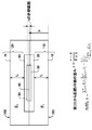
- FIG. 2 is a cross-sectional view for explaining the distortion generated in the solar cell device 100.
- the solar cell device 100 includes seven layers.
- the elastic modulus E and the thickness t of each layer included in the solar cell device 100 are expressed using a natural number i for identifying each layer as a subscript.
- the first elastic layer 10 which is the layer on the first surface 101 side is the first layer
- the elastic modulus of the i-th layer counted from the first elastic layer 10 is E. Represented by i .
- the elastic modulus in the present embodiment is a longitudinal elastic modulus.
- the elastic modulus in the present embodiment may be a longitudinal elastic modulus measured by a bending test.
- the strain ⁇ of the surface separated from the first surface 101 by the distance r is expressed by the following equation.
- R is the radius of curvature of the solar cell device 100.
- b represents the distance from the first surface 101 to the neutral surface. b is expressed by the following equation.
- n indicates the number of layers included in the solar cell device 100.
- E i indicates the elastic modulus of the i-th layer from the first surface 101.
- t i and t j indicate the thickness of the i-th layer and the thickness of the j-th layer, respectively.
- the neutral plane is located between the center of the first electrode layer 30 and the center of the second electrode layer 50 in the thickness direction.
- the thickness t 1 of the first elastic layer 10 and the elasticity are set such that the neutral surface is located between the center of the first electrode layer 30 and the center of the second electrode layer 50 in the thickness direction.
- a rate E 1, and the thickness t 2 and the elastic modulus E 7 of the second elastic layer 70 are defined.
- Table 1 shows parameters used in examples of the solar cell device 100 described later. Each example is characterized by t 1 and modulus E 1 , t 7 and modulus E 7 .
- first film layer 20 and the second film layer 60 may be formed of parylene.
- the second electrode layer 50 may be made of silver.
- ⁇ can be reduced to about 1% or less by setting t 1 to 10 ⁇ m or more. Therefore, t 1 is preferably 10 ⁇ m or more. Further, by setting t 1 to 50 ⁇ m or more, ⁇ can be reduced to about 0.25% or less. Therefore, t 1 is more preferably 50 ⁇ m or more. Further, by setting t 1 to 100 ⁇ m or more, ⁇ can be reduced to about 0.1% or less. Therefore, it is particularly preferable that t 1 is 100 ⁇ m or more.
- t 1 and t 7 is 10 ⁇ m or more, more preferably t 1 and t 7 is 50 ⁇ m or more, and particularly preferably t 1 and t 7 is 100 ⁇ m or more.
- one of t 1 and t 7 may be 10 ⁇ m or more, one of t 1 and t 7 may be 50 ⁇ m or more, and one of t 1 and t 7 may be 100 ⁇ m or more.
- t 1 , E in order to position the neutral plane between the center of the first electrode layer 30 and the center of the second electrode layer 50, t 1 , E
- 1 , t 7 and E 7 are conditioned by two parameters: t 7 / t 1 and (E 7 / E 1 ) ⁇ (t 7 / t 1 ) 2 .
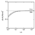
- t1 and E1 in order to locate the neutral plane between the center of the first electrode layer 30 and the center of the second electrode layer 50 when t1 and E1 are set to specific values (E 7 / E 1 ) ⁇ (t 7 / t 1 ) 2 represents the upper and lower limits that can be taken, and t 7 / t 1 is a parameter.
- the line on the “MAX” side in FIG. 4 shows the case where the neutral plane coincides with the center of the second electrode layer 50, and the line on the “MIN” side in FIG. The case where it coincides with the center is shown. That is, the line on the “MAX” side in FIG. 4 is (E 7 / E 1 ) ⁇ (t for positioning the neutral plane between the center of the first electrode layer 30 and the center of the second electrode layer 50. 7 / t 1 ) The upper limit of 2 . Also, the line on the “MIN” side in FIG. 4 indicates (E 7 / E 1 ) ⁇ (t for positioning the neutral plane between the center of the first electrode layer 30 and the center of the second electrode layer 50. 7 / t 1 ) 2 is the lower limit.
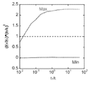
- the meanings of “MAX” and “MIN” in FIGS. 5 to 9 are the same as the meanings of “MAX” and “MIN” in FIG.
- the neutral plane can be positioned between the center of the first electrode layer 30 and the center of the second electrode layer 50. Therefore, it is preferable to satisfy t 7 / t 1 ⁇ 0.2.
- the solar cell device 100 because it has a structure substantially symmetrical with respect to the photoelectric conversion layer 40, it is preferable to satisfy the t 1 / t 7 ⁇ 0.2. Therefore, it is preferable to satisfy 0.2 ⁇ t 7 / t 1 ⁇ 5.
- t 7 / t 1 preferably satisfies 0.2 ⁇ t 7 / t 1 ⁇ 5. It is more preferable to satisfy 0.5 ⁇ t 7 / t 1 ⁇ 2. It is particularly preferable that 0.8 ⁇ t 7 / t 1 ⁇ 1.25 is satisfied.
- the upper limit value and lower limit value of (E 7 / E 1 ) ⁇ (t 7 / t 1 ) 2 necessary for the above can be regarded as constants.
- 0.5 ⁇ (E 7 / E 1 ) ⁇ (t 7 / t 1 ) 2 ⁇ 2 is satisfied.
- 0.5 ⁇ (E 7 / E 1 ) ⁇ (t 7 / t 1 ) 2 ⁇ 2 range, within a range between the constant value of constant values and the upper limit value of the lower limit of (E 7 / E 1) ⁇ (t 7 / t 1).
- the preferred range of (E 7 / E 1 ) ⁇ (t 7 / t 1 ) 2 is examined, so that 0.1 ⁇ (E 7 / E 1 ) ⁇ (t 7 / t 1 ) 2 ⁇ 10 It is preferable to satisfy. It is more preferable to satisfy 0.5 ⁇ (E 7 / E 1 ) ⁇ (t 7 / t 1 ) 2 ⁇ 2. It is particularly preferable that 0.8 ⁇ (E 7 / E 1 ) ⁇ (t 7 / t 1 ) 2 ⁇ 1.25 is satisfied.
- the parameter is between the center of the first electrode layer 30 and the center of the second electrode layer 50. It is easy to position the elevation surface, and it is possible to make it difficult for a difference to occur in the strain applied to the first electrode layer 30 and the second electrode layer 50.
- the thickness t 2 of the first film layer 20 is preferably at least t 2 ⁇ 30 ⁇ m from the viewpoint of followability of the uneven surface and easy adhesion. In order to further improve followability and easy adhesion, it is more preferable that t 2 ⁇ 10 ⁇ m. In order to further improve followability and easy adhesion, it is particularly preferable that t 2 ⁇ 2 ⁇ m.
- the material forming the first elastic layer 10 is not limited to rubber or polymer material.
- the material forming the first elastic layer 10 may be glass.
- the material forming the second elastic layer 70 is not limited to rubber or polymer material.
- the material forming the second elastic layer 70 may be glass.
- the second base material layer 120 includes the second film layer 60 and the second elastic layer 70.
- the second base material layer 120 may not include the second film layer 60.
- the second base material layer 120 may include only the first elastic layer 10.
- the first base material layer 110 includes the first elastic layer 10 and the first film layer 20
- the second base material layer 120 includes the second film layer 60 and the second elastic layer 70.
- at least one of the first base material layer 110 and the second base material layer 120 may be a single layer formed of a single material.
- the semiconductor device is not limited to a solar cell device.
- the semiconductor device may be a light emitting device.
- a light emitting layer may be applied as a semiconductor layer.
- the light emitting layer may include an organic light emitting diode, a light emitting polymer, or the like.
- the semiconductor layer may include both a photoelectric conversion layer and a light emitting layer.
- the semiconductor layer may be a current light emitting layer, an electroluminescent layer, an organic transistor layer, or a combination thereof. Note that the semiconductor layer is not limited to the photoelectric conversion layer and the light emitting layer.
- the semiconductor layer may include an organic semiconductor having various functions different from the photoelectric conversion function and the light emitting function.
- the semiconductor layer may be formed using a semiconductor material such as an organic material, an oxide material, or amorphous silicon.
- a semiconductor material such as an organic material, an oxide material, or amorphous silicon.
- an organic semiconductor material is preferably used from the viewpoint of flexibility and coatability, but a compound semiconductor material such as CIGS or CIS or a perovskite compound material can also be used depending on the purpose.
- the semiconductor device may be a field effect transistor, an integrated circuit, or the like.
- the sensor and its detection circuit, or a secondary battery may be included.
- the semiconductor device may be a power generation device, a lighting device, a display device, electronic paper, a power storage device, a sheet-type sensor device, or a combination thereof.
Landscapes
- Photovoltaic Devices (AREA)
- Life Sciences & Earth Sciences (AREA)
- Engineering & Computer Science (AREA)
- Sustainable Development (AREA)
- Sustainable Energy (AREA)
Priority Applications (1)
| Application Number | Priority Date | Filing Date | Title |
|---|---|---|---|
| US16/529,719 US20190363206A1 (en) | 2017-02-03 | 2019-08-01 | Semiconductor device |
Applications Claiming Priority (2)
| Application Number | Priority Date | Filing Date | Title |
|---|---|---|---|
| JP2017-019126 | 2017-02-03 | ||
| JP2017019126A JP2018125505A (ja) | 2017-02-03 | 2017-02-03 | 半導体デバイス |
Related Child Applications (1)
| Application Number | Title | Priority Date | Filing Date |
|---|---|---|---|
| US16/529,719 Continuation US20190363206A1 (en) | 2017-02-03 | 2019-08-01 | Semiconductor device |
Publications (1)
| Publication Number | Publication Date |
|---|---|
| WO2018143368A1 true WO2018143368A1 (ja) | 2018-08-09 |
Family
ID=63040750
Family Applications (1)
| Application Number | Title | Priority Date | Filing Date |
|---|---|---|---|
| PCT/JP2018/003475 Ceased WO2018143368A1 (ja) | 2017-02-03 | 2018-02-01 | 半導体デバイス |
Country Status (3)
| Country | Link |
|---|---|
| US (1) | US20190363206A1 (https=) |
| JP (1) | JP2018125505A (https=) |
| WO (1) | WO2018143368A1 (https=) |
Families Citing this family (4)
| Publication number | Priority date | Publication date | Assignee | Title |
|---|---|---|---|---|
| EP3739641B1 (en) * | 2019-05-15 | 2025-08-13 | Samsung Electronics Co., Ltd. | N-type semiconductor composition, and thin film, organic photoelectric device, image sensor, and electronic device including the same |
| US11713952B2 (en) | 2019-05-17 | 2023-08-01 | Samsung Electronics Co., Ltd. | Organic photoelectric device, image sensor, and electronic device |
| KR20220093644A (ko) * | 2020-12-28 | 2022-07-05 | 동우 화인켐 주식회사 | 원도우 적층체 및 그 제조 방법 |
| CN120302723A (zh) * | 2024-01-05 | 2025-07-11 | 宁德时代未来能源(上海)研究院有限公司 | 太阳能电池及制备方法、用电设备 |
Citations (7)
| Publication number | Priority date | Publication date | Assignee | Title |
|---|---|---|---|---|
| JPH02113584A (ja) * | 1988-09-01 | 1990-04-25 | Minnesota Mining & Mfg Co <3M> | 曲げても性能の劣化しない薄膜集積回路の製造方法 |
| JP2005251671A (ja) * | 2004-03-08 | 2005-09-15 | Fuji Photo Film Co Ltd | 表示装置 |
| WO2010071123A1 (ja) * | 2008-12-17 | 2010-06-24 | 三洋電機株式会社 | 太陽電池モジュール及びその製造方法 |
| JP2011069812A (ja) * | 2009-08-31 | 2011-04-07 | Mitsui Chemicals Inc | 測定方法、太陽電池モジュールの製造方法、測定装置、太陽電池モジュールおよび太陽電池モジュールの評価方法 |
| US20140367644A1 (en) * | 2013-06-13 | 2014-12-18 | Samsung Display Co., Ltd. | Display apparatus having improved bending properties and method of manufacturing same |
| JP2016111192A (ja) * | 2014-12-05 | 2016-06-20 | トヨタ自動車株式会社 | 太陽電池モジュール |
| WO2017010329A1 (ja) * | 2015-07-10 | 2017-01-19 | シャープ株式会社 | エレクトロルミネッセンス装置 |
Family Cites Families (4)
| Publication number | Priority date | Publication date | Assignee | Title |
|---|---|---|---|---|
| JP2992464B2 (ja) * | 1994-11-04 | 1999-12-20 | キヤノン株式会社 | 集電電極用被覆ワイヤ、該集電電極用被覆ワイヤを用いた光起電力素子及びその製造方法 |
| JP2005311171A (ja) * | 2004-04-23 | 2005-11-04 | Kansai Tlo Kk | 有機半導体デバイス |
| JP2006066762A (ja) * | 2004-08-30 | 2006-03-09 | Canon Inc | フレキシブル太陽電池モジュール及びその施工方法 |
| JP2016197695A (ja) * | 2015-04-06 | 2016-11-24 | 旭硝子株式会社 | 太陽電池モジュール |
-
2017
- 2017-02-03 JP JP2017019126A patent/JP2018125505A/ja active Pending
-
2018
- 2018-02-01 WO PCT/JP2018/003475 patent/WO2018143368A1/ja not_active Ceased
-
2019
- 2019-08-01 US US16/529,719 patent/US20190363206A1/en not_active Abandoned
Patent Citations (7)
| Publication number | Priority date | Publication date | Assignee | Title |
|---|---|---|---|---|
| JPH02113584A (ja) * | 1988-09-01 | 1990-04-25 | Minnesota Mining & Mfg Co <3M> | 曲げても性能の劣化しない薄膜集積回路の製造方法 |
| JP2005251671A (ja) * | 2004-03-08 | 2005-09-15 | Fuji Photo Film Co Ltd | 表示装置 |
| WO2010071123A1 (ja) * | 2008-12-17 | 2010-06-24 | 三洋電機株式会社 | 太陽電池モジュール及びその製造方法 |
| JP2011069812A (ja) * | 2009-08-31 | 2011-04-07 | Mitsui Chemicals Inc | 測定方法、太陽電池モジュールの製造方法、測定装置、太陽電池モジュールおよび太陽電池モジュールの評価方法 |
| US20140367644A1 (en) * | 2013-06-13 | 2014-12-18 | Samsung Display Co., Ltd. | Display apparatus having improved bending properties and method of manufacturing same |
| JP2016111192A (ja) * | 2014-12-05 | 2016-06-20 | トヨタ自動車株式会社 | 太陽電池モジュール |
| WO2017010329A1 (ja) * | 2015-07-10 | 2017-01-19 | シャープ株式会社 | エレクトロルミネッセンス装置 |
Non-Patent Citations (1)
| Title |
|---|
| REUVENY, AMIR ET AL.: "Ultra-flexible short-channel organic field-effect transistors", APPLIED PHYSICS EXPRESS, vol. 8, 28 August 2015 (2015-08-28), pages 091601-1 - 091601-4, XP055530767 * |
Also Published As
| Publication number | Publication date |
|---|---|
| US20190363206A1 (en) | 2019-11-28 |
| JP2018125505A (ja) | 2018-08-09 |
Similar Documents
| Publication | Publication Date | Title |
|---|---|---|
| Yu et al. | Soft human–machine interface sensing displays: materials and devices | |
| WO2018143368A1 (ja) | 半導体デバイス | |
| Park et al. | Graphene-based conformal devices | |
| Song et al. | Fibertronic organic light-emitting diodes toward fully addressable, environmentally robust, wearable displays | |
| Gong et al. | One‐dimensional nanomaterials for soft electronics | |
| Zhang et al. | Mechanics of stretchable batteries and supercapacitors | |
| Zou et al. | Flexible devices: from materials, architectures to applications | |
| JP5850804B2 (ja) | タッチパネル、タッチパネルの製造方法 | |
| Ko et al. | PDMS-based triboelectric and transparent nanogenerators with ZnO nanorod arrays | |
| Karan et al. | An approach to design highly durable piezoelectric nanogenerator based on self‐poled PVDF/AlO‐rGO flexible nanocomposite with high power density and energy conversion efficiency | |
| Noh | Conductive elastomers for stretchable electronics, sensors and energy harvesters | |
| JP2006319333A5 (https=) | ||
| Kang et al. | Recent advances in fiber-shaped electronic devices for wearable applications | |
| US20160293809A1 (en) | Flip chip light emitting diode package structure | |
| EP2728632A3 (en) | Light emitting device and light emitting device array | |
| CN108318162A (zh) | 一种柔性传感器及其制备方法 | |
| CN105006450B (zh) | 一种可延展无机柔性led阵列的制备方法 | |
| CN108444620B (zh) | 一种同层式的多级阵列压力传感器 | |
| US7740376B2 (en) | Flexible light emitting module | |
| CN106298798A (zh) | 柔性显示器件及其制造方法 | |
| Choi et al. | Omnidirectionally stretchable organic transistors for use in wearable electronics: ensuring overall stretchability by applying nonstretchable wrinkled components | |
| EP2418698A3 (en) | Semiconductor light emitting device and method for manufacturing the same | |
| Yoon et al. | Stretchable, bifacial Si-organic hybrid solar cells by vertical array of Si micropillars embedded into elastomeric substrates | |
| CN113664807A (zh) | 一种具有保护功能的柔性电子铠甲及其制造方法与应用 | |
| CN104966791A (zh) | 一种掩膜板及其制造方法、oled器件封装方法 |
Legal Events
| Date | Code | Title | Description |
|---|---|---|---|
| 121 | Ep: the epo has been informed by wipo that ep was designated in this application |
Ref document number: 18748525 Country of ref document: EP Kind code of ref document: A1 |
|
| NENP | Non-entry into the national phase |
Ref country code: DE |
|
| 122 | Ep: pct application non-entry in european phase |
Ref document number: 18748525 Country of ref document: EP Kind code of ref document: A1 |