JP2018125505A - 半導体デバイス - Google Patents
半導体デバイス Download PDFInfo
- Publication number
- JP2018125505A JP2018125505A JP2017019126A JP2017019126A JP2018125505A JP 2018125505 A JP2018125505 A JP 2018125505A JP 2017019126 A JP2017019126 A JP 2017019126A JP 2017019126 A JP2017019126 A JP 2017019126A JP 2018125505 A JP2018125505 A JP 2018125505A
- Authority
- JP
- Japan
- Prior art keywords
- layer
- electrode layer
- semiconductor device
- elastic
- thickness
- Prior art date
- Legal status (The legal status is an assumption and is not a legal conclusion. Google has not performed a legal analysis and makes no representation as to the accuracy of the status listed.)
- Pending
Links
- 239000004065 semiconductor Substances 0.000 title claims abstract description 76
- 239000000463 material Substances 0.000 claims abstract description 78
- 238000006243 chemical reaction Methods 0.000 claims description 22
- 238000002834 transmittance Methods 0.000 claims description 5
- 230000007935 neutral effect Effects 0.000 abstract description 14
- 239000010410 layer Substances 0.000 description 276
- 239000010408 film Substances 0.000 description 37
- 229920005989 resin Polymers 0.000 description 15
- 239000011347 resin Substances 0.000 description 15
- -1 polyethylene Polymers 0.000 description 11
- 229920001971 elastomer Polymers 0.000 description 9
- 239000005060 rubber Substances 0.000 description 9
- 238000005452 bending Methods 0.000 description 8
- 229910052751 metal Inorganic materials 0.000 description 7
- 239000002184 metal Substances 0.000 description 7
- 150000001875 compounds Chemical class 0.000 description 5
- 239000011521 glass Substances 0.000 description 5
- 238000000034 method Methods 0.000 description 5
- 229910052709 silver Inorganic materials 0.000 description 5
- 239000004332 silver Substances 0.000 description 5
- 239000003822 epoxy resin Substances 0.000 description 4
- 229920000647 polyepoxide Polymers 0.000 description 4
- 229920000098 polyolefin Polymers 0.000 description 4
- 238000010248 power generation Methods 0.000 description 4
- 239000010409 thin film Substances 0.000 description 4
- 239000004925 Acrylic resin Substances 0.000 description 3
- 229920000178 Acrylic resin Polymers 0.000 description 3
- OKTJSMMVPCPJKN-UHFFFAOYSA-N Carbon Chemical compound [C] OKTJSMMVPCPJKN-UHFFFAOYSA-N 0.000 description 3
- 241001465754 Metazoa Species 0.000 description 3
- BQCADISMDOOEFD-UHFFFAOYSA-N Silver Chemical compound [Ag] BQCADISMDOOEFD-UHFFFAOYSA-N 0.000 description 3
- 229910052782 aluminium Inorganic materials 0.000 description 3
- XAGFODPZIPBFFR-UHFFFAOYSA-N aluminium Chemical compound [Al] XAGFODPZIPBFFR-UHFFFAOYSA-N 0.000 description 3
- 239000011248 coating agent Substances 0.000 description 3
- 238000000576 coating method Methods 0.000 description 3
- PCHJSUWPFVWCPO-UHFFFAOYSA-N gold Chemical compound [Au] PCHJSUWPFVWCPO-UHFFFAOYSA-N 0.000 description 3
- 229910052737 gold Inorganic materials 0.000 description 3
- 239000010931 gold Substances 0.000 description 3
- 239000002070 nanowire Substances 0.000 description 3
- 229920000052 poly(p-xylylene) Polymers 0.000 description 3
- 229920002857 polybutadiene Polymers 0.000 description 3
- 229920000515 polycarbonate Polymers 0.000 description 3
- 239000004417 polycarbonate Substances 0.000 description 3
- 229920000728 polyester Polymers 0.000 description 3
- 239000002861 polymer material Substances 0.000 description 3
- 230000008569 process Effects 0.000 description 3
- 239000007779 soft material Substances 0.000 description 3
- 239000000758 substrate Substances 0.000 description 3
- XMWRBQBLMFGWIX-UHFFFAOYSA-N C60 fullerene Chemical class C12=C3C(C4=C56)=C7C8=C5C5=C9C%10=C6C6=C4C1=C1C4=C6C6=C%10C%10=C9C9=C%11C5=C8C5=C8C7=C3C3=C7C2=C1C1=C2C4=C6C4=C%10C6=C9C9=C%11C5=C5C8=C3C3=C7C1=C1C2=C4C6=C2C9=C5C3=C12 XMWRBQBLMFGWIX-UHFFFAOYSA-N 0.000 description 2
- RYGMFSIKBFXOCR-UHFFFAOYSA-N Copper Chemical compound [Cu] RYGMFSIKBFXOCR-UHFFFAOYSA-N 0.000 description 2
- 229920000181 Ethylene propylene rubber Polymers 0.000 description 2
- 229920000877 Melamine resin Polymers 0.000 description 2
- 229920000459 Nitrile rubber Polymers 0.000 description 2
- 239000004952 Polyamide Substances 0.000 description 2
- 239000005062 Polybutadiene Substances 0.000 description 2
- 239000004698 Polyethylene Substances 0.000 description 2
- 239000004642 Polyimide Substances 0.000 description 2
- 239000004743 Polypropylene Substances 0.000 description 2
- 239000004793 Polystyrene Substances 0.000 description 2
- 239000004372 Polyvinyl alcohol Substances 0.000 description 2
- 229920001328 Polyvinylidene chloride Polymers 0.000 description 2
- VYPSYNLAJGMNEJ-UHFFFAOYSA-N Silicium dioxide Chemical compound O=[Si]=O VYPSYNLAJGMNEJ-UHFFFAOYSA-N 0.000 description 2
- 229920001807 Urea-formaldehyde Polymers 0.000 description 2
- 229920006311 Urethane elastomer Polymers 0.000 description 2
- XLOMVQKBTHCTTD-UHFFFAOYSA-N Zinc monoxide Chemical compound [Zn]=O XLOMVQKBTHCTTD-UHFFFAOYSA-N 0.000 description 2
- 229920000800 acrylic rubber Polymers 0.000 description 2
- 229920000122 acrylonitrile butadiene styrene Polymers 0.000 description 2
- 229910021417 amorphous silicon Inorganic materials 0.000 description 2
- 150000004945 aromatic hydrocarbons Chemical class 0.000 description 2
- 230000036772 blood pressure Effects 0.000 description 2
- 229910021393 carbon nanotube Inorganic materials 0.000 description 2
- 239000002041 carbon nanotube Substances 0.000 description 2
- 229910052802 copper Inorganic materials 0.000 description 2
- 239000010949 copper Substances 0.000 description 2
- 229920000840 ethylene tetrafluoroethylene copolymer Polymers 0.000 description 2
- 239000006260 foam Substances 0.000 description 2
- LNEPOXFFQSENCJ-UHFFFAOYSA-N haloperidol Chemical compound C1CC(O)(C=2C=CC(Cl)=CC=2)CCN1CCCC(=O)C1=CC=C(F)C=C1 LNEPOXFFQSENCJ-UHFFFAOYSA-N 0.000 description 2
- 230000036541 health Effects 0.000 description 2
- 229920003049 isoprene rubber Polymers 0.000 description 2
- 125000005395 methacrylic acid group Chemical group 0.000 description 2
- 239000005011 phenolic resin Substances 0.000 description 2
- 229920001084 poly(chloroprene) Polymers 0.000 description 2
- 229920000058 polyacrylate Polymers 0.000 description 2
- 229920002647 polyamide Polymers 0.000 description 2
- 238000006068 polycondensation reaction Methods 0.000 description 2
- 229920000573 polyethylene Polymers 0.000 description 2
- 229920001721 polyimide Polymers 0.000 description 2
- 229920000642 polymer Polymers 0.000 description 2
- 229920001155 polypropylene Polymers 0.000 description 2
- 229920002223 polystyrene Polymers 0.000 description 2
- 229920002451 polyvinyl alcohol Polymers 0.000 description 2
- 229920000915 polyvinyl chloride Polymers 0.000 description 2
- 239000004800 polyvinyl chloride Substances 0.000 description 2
- 239000005033 polyvinylidene chloride Substances 0.000 description 2
- 229920002379 silicone rubber Polymers 0.000 description 2
- 229920003048 styrene butadiene rubber Polymers 0.000 description 2
- 229920001187 thermosetting polymer Polymers 0.000 description 2
- 229920006337 unsaturated polyester resin Polymers 0.000 description 2
- SHXCHSNZIGEBFL-UHFFFAOYSA-N 1,3-benzothiazole;zinc Chemical compound [Zn].C1=CC=C2SC=NC2=C1 SHXCHSNZIGEBFL-UHFFFAOYSA-N 0.000 description 1
- UIWLITBBFICQKW-UHFFFAOYSA-N 1h-benzo[h]quinolin-2-one Chemical compound C1=CC=C2C3=NC(O)=CC=C3C=CC2=C1 UIWLITBBFICQKW-UHFFFAOYSA-N 0.000 description 1
- MMHMYFWOECSGDR-UHFFFAOYSA-N 2,5-dimethoxybenzenesulfonamide Chemical compound COC1=CC=C(OC)C(S(N)(=O)=O)=C1 MMHMYFWOECSGDR-UHFFFAOYSA-N 0.000 description 1
- STTGYIUESPWXOW-UHFFFAOYSA-N 2,9-dimethyl-4,7-diphenyl-1,10-phenanthroline Chemical compound C=12C=CC3=C(C=4C=CC=CC=4)C=C(C)N=C3C2=NC(C)=CC=1C1=CC=CC=C1 STTGYIUESPWXOW-UHFFFAOYSA-N 0.000 description 1
- 241001391944 Commicarpus scandens Species 0.000 description 1
- 229920000144 PEDOT:PSS Polymers 0.000 description 1
- GWEVSGVZZGPLCZ-UHFFFAOYSA-N Titan oxide Chemical compound O=[Ti]=O GWEVSGVZZGPLCZ-UHFFFAOYSA-N 0.000 description 1
- 150000001412 amines Chemical class 0.000 description 1
- 238000000149 argon plasma sintering Methods 0.000 description 1
- 230000008901 benefit Effects 0.000 description 1
- 229910052790 beryllium Inorganic materials 0.000 description 1
- ATBAMAFKBVZNFJ-UHFFFAOYSA-N beryllium atom Chemical compound [Be] ATBAMAFKBVZNFJ-UHFFFAOYSA-N 0.000 description 1
- 230000036760 body temperature Effects 0.000 description 1
- 229910052799 carbon Inorganic materials 0.000 description 1
- 239000003575 carbonaceous material Substances 0.000 description 1
- 230000015556 catabolic process Effects 0.000 description 1
- 239000001913 cellulose Substances 0.000 description 1
- 229920002678 cellulose Polymers 0.000 description 1
- 230000001143 conditioned effect Effects 0.000 description 1
- 229920001940 conductive polymer Polymers 0.000 description 1
- 239000004020 conductor Substances 0.000 description 1
- 230000008602 contraction Effects 0.000 description 1
- 238000006731 degradation reaction Methods 0.000 description 1
- 238000013461 design Methods 0.000 description 1
- 238000001514 detection method Methods 0.000 description 1
- 230000006866 deterioration Effects 0.000 description 1
- 150000004985 diamines Chemical class 0.000 description 1
- 239000013013 elastic material Substances 0.000 description 1
- 238000004049 embossing Methods 0.000 description 1
- 239000012765 fibrous filler Substances 0.000 description 1
- 230000005669 field effect Effects 0.000 description 1
- 239000000945 filler Substances 0.000 description 1
- 239000011888 foil Substances 0.000 description 1
- 229910003472 fullerene Inorganic materials 0.000 description 1
- 238000009499 grossing Methods 0.000 description 1
- 230000005525 hole transport Effects 0.000 description 1
- 229910003437 indium oxide Inorganic materials 0.000 description 1
- HJZPJSFRSAHQNT-UHFFFAOYSA-N indium(3+) oxygen(2-) zirconium(4+) Chemical compound [O-2].[Zr+4].[In+3] HJZPJSFRSAHQNT-UHFFFAOYSA-N 0.000 description 1
- PJXISJQVUVHSOJ-UHFFFAOYSA-N indium(iii) oxide Chemical compound [O-2].[O-2].[O-2].[In+3].[In+3] PJXISJQVUVHSOJ-UHFFFAOYSA-N 0.000 description 1
- AMGQUBHHOARCQH-UHFFFAOYSA-N indium;oxotin Chemical compound [In].[Sn]=O AMGQUBHHOARCQH-UHFFFAOYSA-N 0.000 description 1
- 238000002347 injection Methods 0.000 description 1
- 239000007924 injection Substances 0.000 description 1
- 238000004519 manufacturing process Methods 0.000 description 1
- 229910044991 metal oxide Inorganic materials 0.000 description 1
- 150000004706 metal oxides Chemical class 0.000 description 1
- 125000005641 methacryl group Chemical group 0.000 description 1
- 239000000113 methacrylic resin Substances 0.000 description 1
- 229910021424 microcrystalline silicon Inorganic materials 0.000 description 1
- 238000012986 modification Methods 0.000 description 1
- 230000004048 modification Effects 0.000 description 1
- 238000012544 monitoring process Methods 0.000 description 1
- 229910021421 monocrystalline silicon Inorganic materials 0.000 description 1
- 239000002121 nanofiber Substances 0.000 description 1
- 229910000480 nickel oxide Inorganic materials 0.000 description 1
- 239000011368 organic material Substances 0.000 description 1
- 150000004866 oxadiazoles Chemical class 0.000 description 1
- GNRSAWUEBMWBQH-UHFFFAOYSA-N oxonickel Chemical compound [Ni]=O GNRSAWUEBMWBQH-UHFFFAOYSA-N 0.000 description 1
- 150000002964 pentacenes Chemical class 0.000 description 1
- 150000002979 perylenes Chemical class 0.000 description 1
- 238000000016 photochemical curing Methods 0.000 description 1
- 229920002120 photoresistant polymer Polymers 0.000 description 1
- 229920003207 poly(ethylene-2,6-naphthalate) Polymers 0.000 description 1
- 229910021420 polycrystalline silicon Inorganic materials 0.000 description 1
- 239000011112 polyethylene naphthalate Substances 0.000 description 1
- 229920000139 polyethylene terephthalate Polymers 0.000 description 1
- 239000005020 polyethylene terephthalate Substances 0.000 description 1
- 150000004032 porphyrins Chemical class 0.000 description 1
- 238000007789 sealing Methods 0.000 description 1
- 239000003566 sealing material Substances 0.000 description 1
- 239000000377 silicon dioxide Substances 0.000 description 1
- 239000002356 single layer Substances 0.000 description 1
- 238000003860 storage Methods 0.000 description 1
- 238000012360 testing method Methods 0.000 description 1
- 229930192474 thiophene Natural products 0.000 description 1
- 150000003577 thiophenes Chemical class 0.000 description 1
- XOLBLPGZBRYERU-UHFFFAOYSA-N tin dioxide Chemical compound O=[Sn]=O XOLBLPGZBRYERU-UHFFFAOYSA-N 0.000 description 1
- 229910001887 tin oxide Inorganic materials 0.000 description 1
- OGIDPMRJRNCKJF-UHFFFAOYSA-N titanium oxide Inorganic materials [Ti]=O OGIDPMRJRNCKJF-UHFFFAOYSA-N 0.000 description 1
- 125000006839 xylylene group Chemical group 0.000 description 1
- 239000011787 zinc oxide Substances 0.000 description 1
Images


Classifications
-
- H—ELECTRICITY
- H01—ELECTRIC ELEMENTS
- H01L—SEMICONDUCTOR DEVICES NOT COVERED BY CLASS H10
- H01L31/00—Semiconductor devices sensitive to infrared radiation, light, electromagnetic radiation of shorter wavelength or corpuscular radiation and specially adapted either for the conversion of the energy of such radiation into electrical energy or for the control of electrical energy by such radiation; Processes or apparatus specially adapted for the manufacture or treatment thereof or of parts thereof; Details thereof
- H01L31/02—Details
- H01L31/0224—Electrodes
- H01L31/022408—Electrodes for devices characterised by at least one potential jump barrier or surface barrier
- H01L31/022425—Electrodes for devices characterised by at least one potential jump barrier or surface barrier for solar cells
-
- H—ELECTRICITY
- H01—ELECTRIC ELEMENTS
- H01L—SEMICONDUCTOR DEVICES NOT COVERED BY CLASS H10
- H01L31/00—Semiconductor devices sensitive to infrared radiation, light, electromagnetic radiation of shorter wavelength or corpuscular radiation and specially adapted either for the conversion of the energy of such radiation into electrical energy or for the control of electrical energy by such radiation; Processes or apparatus specially adapted for the manufacture or treatment thereof or of parts thereof; Details thereof
- H01L31/04—Semiconductor devices sensitive to infrared radiation, light, electromagnetic radiation of shorter wavelength or corpuscular radiation and specially adapted either for the conversion of the energy of such radiation into electrical energy or for the control of electrical energy by such radiation; Processes or apparatus specially adapted for the manufacture or treatment thereof or of parts thereof; Details thereof adapted as photovoltaic [PV] conversion devices
- H01L31/042—PV modules or arrays of single PV cells
- H01L31/0445—PV modules or arrays of single PV cells including thin film solar cells, e.g. single thin film a-Si, CIS or CdTe solar cells
-
- H—ELECTRICITY
- H01—ELECTRIC ELEMENTS
- H01L—SEMICONDUCTOR DEVICES NOT COVERED BY CLASS H10
- H01L31/00—Semiconductor devices sensitive to infrared radiation, light, electromagnetic radiation of shorter wavelength or corpuscular radiation and specially adapted either for the conversion of the energy of such radiation into electrical energy or for the control of electrical energy by such radiation; Processes or apparatus specially adapted for the manufacture or treatment thereof or of parts thereof; Details thereof
- H01L31/02—Details
- H01L31/0224—Electrodes
-
- H—ELECTRICITY
- H01—ELECTRIC ELEMENTS
- H01L—SEMICONDUCTOR DEVICES NOT COVERED BY CLASS H10
- H01L31/00—Semiconductor devices sensitive to infrared radiation, light, electromagnetic radiation of shorter wavelength or corpuscular radiation and specially adapted either for the conversion of the energy of such radiation into electrical energy or for the control of electrical energy by such radiation; Processes or apparatus specially adapted for the manufacture or treatment thereof or of parts thereof; Details thereof
- H01L31/04—Semiconductor devices sensitive to infrared radiation, light, electromagnetic radiation of shorter wavelength or corpuscular radiation and specially adapted either for the conversion of the energy of such radiation into electrical energy or for the control of electrical energy by such radiation; Processes or apparatus specially adapted for the manufacture or treatment thereof or of parts thereof; Details thereof adapted as photovoltaic [PV] conversion devices
- H01L31/042—PV modules or arrays of single PV cells
- H01L31/048—Encapsulation of modules
- H01L31/0481—Encapsulation of modules characterised by the composition of the encapsulation material
-
- H—ELECTRICITY
- H01—ELECTRIC ELEMENTS
- H01L—SEMICONDUCTOR DEVICES NOT COVERED BY CLASS H10
- H01L31/00—Semiconductor devices sensitive to infrared radiation, light, electromagnetic radiation of shorter wavelength or corpuscular radiation and specially adapted either for the conversion of the energy of such radiation into electrical energy or for the control of electrical energy by such radiation; Processes or apparatus specially adapted for the manufacture or treatment thereof or of parts thereof; Details thereof
- H01L31/18—Processes or apparatus specially adapted for the manufacture or treatment of these devices or of parts thereof
- H01L31/1884—Manufacture of transparent electrodes, e.g. TCO, ITO
-
- H—ELECTRICITY
- H10—SEMICONDUCTOR DEVICES; ELECTRIC SOLID-STATE DEVICES NOT OTHERWISE PROVIDED FOR
- H10K—ORGANIC ELECTRIC SOLID-STATE DEVICES
- H10K77/00—Constructional details of devices covered by this subclass and not covered by groups H10K10/80, H10K30/80, H10K50/80 or H10K59/80
- H10K77/10—Substrates, e.g. flexible substrates
- H10K77/111—Flexible substrates
-
- H—ELECTRICITY
- H01—ELECTRIC ELEMENTS
- H01L—SEMICONDUCTOR DEVICES NOT COVERED BY CLASS H10
- H01L31/00—Semiconductor devices sensitive to infrared radiation, light, electromagnetic radiation of shorter wavelength or corpuscular radiation and specially adapted either for the conversion of the energy of such radiation into electrical energy or for the control of electrical energy by such radiation; Processes or apparatus specially adapted for the manufacture or treatment thereof or of parts thereof; Details thereof
- H01L31/18—Processes or apparatus specially adapted for the manufacture or treatment of these devices or of parts thereof
- H01L31/1804—Processes or apparatus specially adapted for the manufacture or treatment of these devices or of parts thereof comprising only elements of Group IV of the Periodic System
- H01L31/182—Special manufacturing methods for polycrystalline Si, e.g. Si ribbon, poly Si ingots, thin films of polycrystalline Si
-
- Y—GENERAL TAGGING OF NEW TECHNOLOGICAL DEVELOPMENTS; GENERAL TAGGING OF CROSS-SECTIONAL TECHNOLOGIES SPANNING OVER SEVERAL SECTIONS OF THE IPC; TECHNICAL SUBJECTS COVERED BY FORMER USPC CROSS-REFERENCE ART COLLECTIONS [XRACs] AND DIGESTS
- Y02—TECHNOLOGIES OR APPLICATIONS FOR MITIGATION OR ADAPTATION AGAINST CLIMATE CHANGE
- Y02E—REDUCTION OF GREENHOUSE GAS [GHG] EMISSIONS, RELATED TO ENERGY GENERATION, TRANSMISSION OR DISTRIBUTION
- Y02E10/00—Energy generation through renewable energy sources
- Y02E10/50—Photovoltaic [PV] energy
- Y02E10/549—Organic PV cells
Abstract
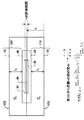
【解決手段】半導体デバイスは、弾性を有する第1基材層と、第1基材層上に設けられた第1電極層と、第1電極層上に設けられた半導体層と、半導体層上に設けられた第2電極層と、第2電極層上に設けられ、弾性を有する第2基材層とを備え、半導体デバイスの厚さ方向において、中立面が、厚さ方向において第1電極層の中心と第2電極層の中心との間に位置し、nは、半導体デバイスが備える層の数を示し、Eiは、半導体デバイスが備える層のうち、半導体デバイスの一方の側からi番目の層の弾性率を示し、ti及びtjは、それぞれi番目の層の厚さ及びj番目の層の厚さを示す。
【選択図】図2
Description
非特許文献1 Martin Kaltenbrunner, Tsuyoshi Sekitani, Jonathan Reeder, Tomoyuki Yokota, Kazunori Kuribara, Takeyoshi Tokuhara, Michael Drack, Reinhard Schwodiauer, Ingrid Graz, Simona Bauer-Gogonea, Siegfried Bauer, Takao Someya, "An ultra-lightweight design for imperceptible plastic electronics", Nature, 499, (7459), 458-463, 2013.
このようなフレキシブル電子回路に、フレキシブルなセンサー類、発電素子、発光素子、二次電池などを組み合わせたフレキシブルシートデバイスが提案されている。この種のシートデバイスでは、軽量かつフレキシブルな特徴を活かし、衣類あるいは体表に直接装着するウエアラブルデバイスとして、人間や動物の体温、脈拍、体水分率、血圧などの健康指標などをモニタリングの上、データ発信もしくは記録し、健康医療に役立てる試みが注目を集めている。ウエアラブルデバイスにおいては、人間あるいは動物の動きに追随し、脱着の際の曲げに耐えて性能等の劣化を引き起こさずに一定期間使用出来ることが求められる。

10 第1弾性層
20 第1フィルム層
30 第1電極層
40 光電変換層
50 第2電極層
60 第2フィルム層
70 第2弾性層
101 第1の面
102 第2の面
110 第1基材層
120 第2基材層
Claims (12)
- 半導体デバイスであって、
弾性を有する第1基材層と、
前記第1基材層上に設けられた第1電極層と、
前記第1電極層上に設けられた半導体層と、
前記半導体層上に設けられた第2電極層と、
前記第2電極層上に設けられ、弾性を有する第2基材層と
を備え、
前記半導体デバイスの厚さ方向において、前記半導体デバイスの一方の面から距離bが
nは、前記半導体デバイスが備える層の数を示し、
Eiは、前記半導体デバイスが備える層のうち、前記半導体デバイスの前記一方の面の側からi番目の層の弾性率を示し、
ti及びtjは、それぞれi番目の層の厚さ及びj番目の層の厚さを示す
半導体デバイス。 - 前記第1基材層は、
第1弾性層と、
前記第1弾性層上に設けられた第1フィルム層と
を備え、
前記第1電極層は、前記第1フィルム層上に設けられ、
前記第2基材層は、
前記第2電極層上に設けられた第2フィルム層と、
前記第2フィルム層上に設けられた第2弾性層と
を備える請求項1に記載の半導体デバイス。 - 前記第1弾性層の弾性率をE1、厚さをt1、前記第2弾性層の弾性率をE7、厚さをt7としたときに、
0.2≦t7/t1≦5
かつ
0.1≦(E7/E1)×(t7/t1)2≦10
を満たす請求項2に記載の半導体デバイス。 - 0.5≦(E7/E1)×(t7/t1)2≦2
を満たす請求項3に記載の半導体デバイス。 - 0.8≦(E7/E1)×(t7/t1)2≦1.25
を満たす請求項3又は4に記載の半導体デバイス。 - 0.5≦t7/t1≦2
を満たす請求項3から5のいずれか一項に記載の半導体デバイス。 - 0.8≦t7/t1≦1.25
を満たす請求項3から6のいずれか一項に記載の半導体デバイス。 - 前記第1弾性層の厚さをt1、前記第2弾性層の厚さをt7としたときに、
t1及びt7の少なくとも一方が、10μm以上である
請求項2から7のいずれか一項に記載の半導体デバイス。 - 前記第1弾性層の厚さをt1、前記第2弾性層の厚さをt7としたときに、
t1及びt7の少なくとも一方が、50μm以上である
請求項2から8のいずれか一項に記載の半導体デバイス。 - 前記第1弾性層の厚さをt1、前記第2弾性層の厚さをt7としたときに、
t1及びt7の少なくとも一方が、100μm以上である
請求項2から9のいずれか一項に記載の半導体デバイス。 - 前記第1電極層は、透明電極層であり、
前記第1基材層は、光透過性を有する
請求項1から10のいずれか一項に記載の半導体デバイス。 - 前記半導体層は、光電変換層である
請求項11に記載の半導体デバイス。
Priority Applications (3)
| Application Number | Priority Date | Filing Date | Title |
|---|---|---|---|
| JP2017019126A JP2018125505A (ja) | 2017-02-03 | 2017-02-03 | 半導体デバイス |
| PCT/JP2018/003475 WO2018143368A1 (ja) | 2017-02-03 | 2018-02-01 | 半導体デバイス |
| US16/529,719 US20190363206A1 (en) | 2017-02-03 | 2019-08-01 | Semiconductor device |
Applications Claiming Priority (1)
| Application Number | Priority Date | Filing Date | Title |
|---|---|---|---|
| JP2017019126A JP2018125505A (ja) | 2017-02-03 | 2017-02-03 | 半導体デバイス |
Publications (2)
| Publication Number | Publication Date |
|---|---|
| JP2018125505A true JP2018125505A (ja) | 2018-08-09 |
| JP2018125505A5 JP2018125505A5 (ja) | 2020-07-09 |
Family
ID=63040750
Family Applications (1)
| Application Number | Title | Priority Date | Filing Date |
|---|---|---|---|
| JP2017019126A Pending JP2018125505A (ja) | 2017-02-03 | 2017-02-03 | 半導体デバイス |
Country Status (3)
| Country | Link |
|---|---|
| US (1) | US20190363206A1 (ja) |
| JP (1) | JP2018125505A (ja) |
| WO (1) | WO2018143368A1 (ja) |
Families Citing this family (2)
| Publication number | Priority date | Publication date | Assignee | Title |
|---|---|---|---|---|
| EP3739641A1 (en) * | 2019-05-15 | 2020-11-18 | Samsung Electronics Co., Ltd. | N-type semiconductor composition, and thin film, organic photoelectric device, image sensor, and electronic device including the same |
| EP3739643A1 (en) | 2019-05-17 | 2020-11-18 | Samsung Electronics Co., Ltd. | Organic photoelectric device, image sensor, and electronic device |
Citations (11)
| Publication number | Priority date | Publication date | Assignee | Title |
|---|---|---|---|---|
| JPH02113584A (ja) * | 1988-09-01 | 1990-04-25 | Minnesota Mining & Mfg Co <3M> | 曲げても性能の劣化しない薄膜集積回路の製造方法 |
| JPH08236796A (ja) * | 1994-11-04 | 1996-09-13 | Canon Inc | 集電電極並びに該集電電極を用いた光起電力素子及びその製造方法 |
| JP2005251671A (ja) * | 2004-03-08 | 2005-09-15 | Fuji Photo Film Co Ltd | 表示装置 |
| JP2005311171A (ja) * | 2004-04-23 | 2005-11-04 | Kansai Tlo Kk | 有機半導体デバイス |
| JP2006066762A (ja) * | 2004-08-30 | 2006-03-09 | Canon Inc | フレキシブル太陽電池モジュール及びその施工方法 |
| WO2010071123A1 (ja) * | 2008-12-17 | 2010-06-24 | 三洋電機株式会社 | 太陽電池モジュール及びその製造方法 |
| JP2011069812A (ja) * | 2009-08-31 | 2011-04-07 | Mitsui Chemicals Inc | 測定方法、太陽電池モジュールの製造方法、測定装置、太陽電池モジュールおよび太陽電池モジュールの評価方法 |
| US20140367644A1 (en) * | 2013-06-13 | 2014-12-18 | Samsung Display Co., Ltd. | Display apparatus having improved bending properties and method of manufacturing same |
| JP2016111192A (ja) * | 2014-12-05 | 2016-06-20 | トヨタ自動車株式会社 | 太陽電池モジュール |
| JP2016197695A (ja) * | 2015-04-06 | 2016-11-24 | 旭硝子株式会社 | 太陽電池モジュール |
| WO2017010329A1 (ja) * | 2015-07-10 | 2017-01-19 | シャープ株式会社 | エレクトロルミネッセンス装置 |
-
2017
- 2017-02-03 JP JP2017019126A patent/JP2018125505A/ja active Pending
-
2018
- 2018-02-01 WO PCT/JP2018/003475 patent/WO2018143368A1/ja active Application Filing
-
2019
- 2019-08-01 US US16/529,719 patent/US20190363206A1/en not_active Abandoned
Patent Citations (11)
| Publication number | Priority date | Publication date | Assignee | Title |
|---|---|---|---|---|
| JPH02113584A (ja) * | 1988-09-01 | 1990-04-25 | Minnesota Mining & Mfg Co <3M> | 曲げても性能の劣化しない薄膜集積回路の製造方法 |
| JPH08236796A (ja) * | 1994-11-04 | 1996-09-13 | Canon Inc | 集電電極並びに該集電電極を用いた光起電力素子及びその製造方法 |
| JP2005251671A (ja) * | 2004-03-08 | 2005-09-15 | Fuji Photo Film Co Ltd | 表示装置 |
| JP2005311171A (ja) * | 2004-04-23 | 2005-11-04 | Kansai Tlo Kk | 有機半導体デバイス |
| JP2006066762A (ja) * | 2004-08-30 | 2006-03-09 | Canon Inc | フレキシブル太陽電池モジュール及びその施工方法 |
| WO2010071123A1 (ja) * | 2008-12-17 | 2010-06-24 | 三洋電機株式会社 | 太陽電池モジュール及びその製造方法 |
| JP2011069812A (ja) * | 2009-08-31 | 2011-04-07 | Mitsui Chemicals Inc | 測定方法、太陽電池モジュールの製造方法、測定装置、太陽電池モジュールおよび太陽電池モジュールの評価方法 |
| US20140367644A1 (en) * | 2013-06-13 | 2014-12-18 | Samsung Display Co., Ltd. | Display apparatus having improved bending properties and method of manufacturing same |
| JP2016111192A (ja) * | 2014-12-05 | 2016-06-20 | トヨタ自動車株式会社 | 太陽電池モジュール |
| JP2016197695A (ja) * | 2015-04-06 | 2016-11-24 | 旭硝子株式会社 | 太陽電池モジュール |
| WO2017010329A1 (ja) * | 2015-07-10 | 2017-01-19 | シャープ株式会社 | エレクトロルミネッセンス装置 |
Non-Patent Citations (1)
| Title |
|---|
| REUVENY AMIR ET AL.: "Ultra-flexible short-channel organic field-effect transistors", APPLIED PHYSICS EXPRESS, vol. 8, JPN6020044797, 28 August 2015 (2015-08-28), pages 091601 - 1, ISSN: 0004606676 * |
Also Published As
| Publication number | Publication date |
|---|---|
| WO2018143368A1 (ja) | 2018-08-09 |
| US20190363206A1 (en) | 2019-11-28 |
Similar Documents
| Publication | Publication Date | Title |
|---|---|---|
| Zhang et al. | Mechanics of stretchable batteries and supercapacitors | |
| Gong et al. | One‐dimensional nanomaterials for soft electronics | |
| Zou et al. | Flexible devices: from materials, architectures to applications | |
| Lee et al. | Wireless powered wearable micro light-emitting diodes | |
| Kim et al. | Graphene for flexible and wearable device applications | |
| Li et al. | Materials and designs for power supply systems in skin-interfaced electronics | |
| Wu et al. | Energy harvesters for wearable and stretchable electronics: from flexibility to stretchability | |
| Gao et al. | A self-healable bifunctional electronic skin | |
| Song et al. | Fibertronic organic light-emitting diodes toward fully addressable, environmentally robust, wearable displays | |
| Zeng et al. | Fiber‐based wearable electronics: a review of materials, fabrication, devices, and applications | |
| US20150185889A1 (en) | Touch panel and method of manufacturing the touch panel | |
| EP2728632A3 (en) | Light emitting device and light emitting device array | |
| WO2018143368A1 (ja) | 半導体デバイス | |
| WO2019000935A1 (zh) | 压力传感器及其制作方法、电子器件 | |
| Lee et al. | Stretchable array of CdSe/ZnS quantum-dot light emitting diodes for visual display of bio-signals | |
| JP2006179867A5 (ja) | ||
| US7740376B2 (en) | Flexible light emitting module | |
| Kang et al. | Recent advances in fiber-shaped electronic devices for wearable applications | |
| CN106298798A (zh) | 柔性显示器件及其制造方法 | |
| Shin et al. | SnO2 nanowire logic devices on deformable nonplanar substrates | |
| Yu et al. | Soft human–machine interface sensing displays: materials and devices | |
| KR102394657B1 (ko) | 유기 광전 소자 및 유기 광전 소자를 제조하기 위한 방법 | |
| Choi et al. | Omnidirectionally stretchable organic transistors for use in wearable electronics: ensuring overall stretchability by applying nonstretchable wrinkled components | |
| Rathore et al. | Bending fatigue damage reduction in indium tin oxide (ITO) by polyimide and ethylene vinyl acetate encapsulation for flexible solar cells | |
| CN108470757B (zh) | 一种显示器件及其封装方法、显示装置 |
Legal Events
| Date | Code | Title | Description |
|---|---|---|---|
| A621 | Written request for application examination |
Free format text: JAPANESE INTERMEDIATE CODE: A621 Effective date: 20200131 |
|
| A521 | Request for written amendment filed |
Free format text: JAPANESE INTERMEDIATE CODE: A523 Effective date: 20200528 |
|
| A131 | Notification of reasons for refusal |
Free format text: JAPANESE INTERMEDIATE CODE: A131 Effective date: 20201201 |
|
| A521 | Request for written amendment filed |
Free format text: JAPANESE INTERMEDIATE CODE: A523 Effective date: 20210129 |
|
| A131 | Notification of reasons for refusal |
Free format text: JAPANESE INTERMEDIATE CODE: A131 Effective date: 20210309 |
|
| A02 | Decision of refusal |
Free format text: JAPANESE INTERMEDIATE CODE: A02 Effective date: 20211005 |