WO2018135044A1 - 検査方法、検査装置、及びマーキング形成方法 - Google Patents
検査方法、検査装置、及びマーキング形成方法 Download PDFInfo
- Publication number
- WO2018135044A1 WO2018135044A1 PCT/JP2017/035848 JP2017035848W WO2018135044A1 WO 2018135044 A1 WO2018135044 A1 WO 2018135044A1 JP 2017035848 W JP2017035848 W JP 2017035848W WO 2018135044 A1 WO2018135044 A1 WO 2018135044A1
- Authority
- WO
- WIPO (PCT)
- Prior art keywords
- marking
- semiconductor device
- substrate
- image
- laser
- Prior art date
- Legal status (The legal status is an assumption and is not a legal conclusion. Google has not performed a legal analysis and makes no representation as to the accuracy of the status listed.)
- Ceased
Links
Images





Classifications
-
- H—ELECTRICITY
- H10—SEMICONDUCTOR DEVICES; ELECTRIC SOLID-STATE DEVICES NOT OTHERWISE PROVIDED FOR
- H10P—GENERIC PROCESSES OR APPARATUS FOR THE MANUFACTURE OR TREATMENT OF DEVICES COVERED BY CLASS H10
- H10P74/00—Testing or measuring during manufacture or treatment of wafers, substrates or devices
- H10P74/23—Testing or measuring during manufacture or treatment of wafers, substrates or devices characterised by multiple measurements, corrections, marking or sorting processes
- H10P74/238—Testing or measuring during manufacture or treatment of wafers, substrates or devices characterised by multiple measurements, corrections, marking or sorting processes comprising acting in response to an ongoing measurement without interruption of processing, e.g. endpoint detection or in-situ thickness measurement
-
- G—PHYSICS
- G01—MEASURING; TESTING
- G01R—MEASURING ELECTRIC VARIABLES; MEASURING MAGNETIC VARIABLES
- G01R31/00—Arrangements for testing electric properties; Arrangements for locating electric faults; Arrangements for electrical testing characterised by what is being tested not provided for elsewhere
- G01R31/28—Testing of electronic circuits, e.g. by signal tracer
- G01R31/302—Contactless testing
- G01R31/308—Contactless testing using non-ionising electromagnetic radiation, e.g. optical radiation
- G01R31/311—Contactless testing using non-ionising electromagnetic radiation, e.g. optical radiation of integrated circuits
-
- H—ELECTRICITY
- H10—SEMICONDUCTOR DEVICES; ELECTRIC SOLID-STATE DEVICES NOT OTHERWISE PROVIDED FOR
- H10P—GENERIC PROCESSES OR APPARATUS FOR THE MANUFACTURE OR TREATMENT OF DEVICES COVERED BY CLASS H10
- H10P74/00—Testing or measuring during manufacture or treatment of wafers, substrates or devices
- H10P74/20—Testing or measuring during manufacture or treatment of wafers, substrates or devices characterised by the properties tested or measured, e.g. structural or electrical properties
- H10P74/203—Structural properties, e.g. testing or measuring thicknesses, line widths, warpage, bond strengths or physical defects
-
- G—PHYSICS
- G01—MEASURING; TESTING
- G01R—MEASURING ELECTRIC VARIABLES; MEASURING MAGNETIC VARIABLES
- G01R31/00—Arrangements for testing electric properties; Arrangements for locating electric faults; Arrangements for electrical testing characterised by what is being tested not provided for elsewhere
- G01R31/28—Testing of electronic circuits, e.g. by signal tracer
- G01R31/2832—Specific tests of electronic circuits not provided for elsewhere
- G01R31/2836—Fault-finding or characterising
-
- H—ELECTRICITY
- H10—SEMICONDUCTOR DEVICES; ELECTRIC SOLID-STATE DEVICES NOT OTHERWISE PROVIDED FOR
- H10P—GENERIC PROCESSES OR APPARATUS FOR THE MANUFACTURE OR TREATMENT OF DEVICES COVERED BY CLASS H10
- H10P34/00—Irradiation with electromagnetic or particle radiation of wafers, substrates or parts of devices
- H10P34/40—Irradiation with electromagnetic or particle radiation of wafers, substrates or parts of devices with high-energy radiation
- H10P34/42—Irradiation with electromagnetic or particle radiation of wafers, substrates or parts of devices with high-energy radiation with electromagnetic radiation, e.g. laser annealing
-
- H—ELECTRICITY
- H10—SEMICONDUCTOR DEVICES; ELECTRIC SOLID-STATE DEVICES NOT OTHERWISE PROVIDED FOR
- H10P—GENERIC PROCESSES OR APPARATUS FOR THE MANUFACTURE OR TREATMENT OF DEVICES COVERED BY CLASS H10
- H10P72/00—Handling or holding of wafers, substrates or devices during manufacture or treatment thereof
- H10P72/04—Apparatus for manufacture or treatment
- H10P72/0431—Apparatus for thermal treatment
- H10P72/0436—Apparatus for thermal treatment mainly by radiation
-
- H—ELECTRICITY
- H10—SEMICONDUCTOR DEVICES; ELECTRIC SOLID-STATE DEVICES NOT OTHERWISE PROVIDED FOR
- H10P—GENERIC PROCESSES OR APPARATUS FOR THE MANUFACTURE OR TREATMENT OF DEVICES COVERED BY CLASS H10
- H10P72/00—Handling or holding of wafers, substrates or devices during manufacture or treatment thereof
- H10P72/06—Apparatus for monitoring, sorting, marking, testing or measuring
- H10P72/0606—Position monitoring, e.g. misposition detection or presence detection
-
- H—ELECTRICITY
- H10—SEMICONDUCTOR DEVICES; ELECTRIC SOLID-STATE DEVICES NOT OTHERWISE PROVIDED FOR
- H10P—GENERIC PROCESSES OR APPARATUS FOR THE MANUFACTURE OR TREATMENT OF DEVICES COVERED BY CLASS H10
- H10P72/00—Handling or holding of wafers, substrates or devices during manufacture or treatment thereof
- H10P72/06—Apparatus for monitoring, sorting, marking, testing or measuring
- H10P72/0614—Marking devices
-
- H—ELECTRICITY
- H10—SEMICONDUCTOR DEVICES; ELECTRIC SOLID-STATE DEVICES NOT OTHERWISE PROVIDED FOR
- H10P—GENERIC PROCESSES OR APPARATUS FOR THE MANUFACTURE OR TREATMENT OF DEVICES COVERED BY CLASS H10
- H10P74/00—Testing or measuring during manufacture or treatment of wafers, substrates or devices
- H10P74/27—Structural arrangements therefor
-
- H—ELECTRICITY
- H10—SEMICONDUCTOR DEVICES; ELECTRIC SOLID-STATE DEVICES NOT OTHERWISE PROVIDED FOR
- H10P—GENERIC PROCESSES OR APPARATUS FOR THE MANUFACTURE OR TREATMENT OF DEVICES COVERED BY CLASS H10
- H10P74/00—Testing or measuring during manufacture or treatment of wafers, substrates or devices
- H10P74/27—Structural arrangements therefor
- H10P74/273—Interconnections for measuring or testing, e.g. probe pads
-
- H—ELECTRICITY
- H10—SEMICONDUCTOR DEVICES; ELECTRIC SOLID-STATE DEVICES NOT OTHERWISE PROVIDED FOR
- H10W—GENERIC PACKAGES, INTERCONNECTIONS, CONNECTORS OR OTHER CONSTRUCTIONAL DETAILS OF DEVICES COVERED BY CLASS H10
- H10W46/00—Marks applied to devices, e.g. for alignment or identification
-
- H—ELECTRICITY
- H10—SEMICONDUCTOR DEVICES; ELECTRIC SOLID-STATE DEVICES NOT OTHERWISE PROVIDED FOR
- H10W—GENERIC PACKAGES, INTERCONNECTIONS, CONNECTORS OR OTHER CONSTRUCTIONAL DETAILS OF DEVICES COVERED BY CLASS H10
- H10W46/00—Marks applied to devices, e.g. for alignment or identification
- H10W46/301—Marks applied to devices, e.g. for alignment or identification for alignment
-
- H—ELECTRICITY
- H10—SEMICONDUCTOR DEVICES; ELECTRIC SOLID-STATE DEVICES NOT OTHERWISE PROVIDED FOR
- H10W—GENERIC PACKAGES, INTERCONNECTIONS, CONNECTORS OR OTHER CONSTRUCTIONAL DETAILS OF DEVICES COVERED BY CLASS H10
- H10W72/00—Interconnections or connectors in packages
- H10W72/01—Manufacture or treatment
- H10W72/012—Manufacture or treatment of bump connectors, dummy bumps or thermal bumps
Definitions
- One aspect of the present invention relates to a semiconductor device inspection method, inspection apparatus, and marking formation method.
- Patent Document 1 discloses a failure analysis apparatus that analyzes a failure position of a semiconductor device using an SiC substrate by an OBIRCH (Optical Beam Induced Resistance Change) method. Patent Document 1 discloses that laser marking is performed on devices and circuits on the front surface side of a substrate by irradiating laser light from the back surface side.
- OBIRCH Optical Beam Induced Resistance Change
- Patent Document 1 does not disclose the detailed position of the marking.
- the marking position may be confirmed from the front surface side or may be confirmed from the back surface side. Therefore, it is preferable that the position where the marking is formed is a position that can be easily confirmed from both the front surface side and the back surface side.
- one aspect of the present invention is an inspection method, an inspection apparatus, and the like that can easily confirm the marking position from either the front side or the back side during physical analysis when performing laser marking from the substrate side of the semiconductor device. And it aims at providing the marking formation method.
- An inspection method is an inspection method for performing laser marking on a semiconductor device having a substrate and a metal layer formed on the substrate, and the semiconductor device is inspected so that a predetermined position in the semiconductor device is obtained. And irradiating the semiconductor device from the substrate side with a laser beam having a wavelength that transmits the substrate so that a marking is formed at least at the boundary between the substrate and the metal layer based on the predetermined position. .
- a laser beam having a wavelength that passes through the substrate is on the substrate side so that a marking is formed at least at the boundary between the substrate and the metal layer based on a predetermined position (for example, a failure location) specified in the semiconductor device.
- a predetermined position for example, a failure location
- the marking can be formed at a position that can be easily confirmed from either the front surface side (metal layer side) or the back surface side (substrate side). it can.
- laser marking is performed from the substrate side of the semiconductor device, it is possible to easily confirm the marking position from either the front side or the back side during physical analysis.
- the irradiation of the laser beam may be controlled so that the marking does not penetrate the metal layer.
- the marking can be kept inside the semiconductor device.
- the irradiation of the laser beam may be controlled so that at least one of a cavity, a modification, and a melting occurs as a marking. Thereby, marking can be formed appropriately.
- the inspection method may further include a step of obtaining a pattern image of a semiconductor device including a mark image indicating marking.
- ascertain a marking position visually with the pattern (for example, wiring pattern) of a semiconductor device is acquirable.
- Such a pattern image makes it possible to easily grasp the marking position in physical analysis.
- the inspection method may further include a step of acquiring position information for specifying a marking position based on the pattern image, and a step of outputting the position information.
- position information for specifying a marking position in physical analysis can be output to an external device or the like. Therefore, for example, even when an inspection apparatus that performs marking and an analysis apparatus that performs physical analysis are arranged at different locations, positional information necessary for performing physical analysis is appropriately transferred to the analysis apparatus. be able to.
- the position information information indicating the relative position of the marking based on the position of the feature point of the semiconductor device may be acquired as the position information.
- the inspection method may further include a step of thinning the substrate and observing the semiconductor device from the thinned substrate side after the step of irradiating the laser beam.
- a step of thinning the substrate By reducing the thickness of the substrate, the marking position can be easily confirmed in the above-described observation step. Thereby, a physical analysis can be accurately performed based on the marking position.
- An inspection apparatus is an inspection apparatus that performs laser marking on a semiconductor device having a substrate and a metal layer formed on the substrate, and is an observation optical that transmits light from the substrate side of the semiconductor device.
- System an optical detector for detecting light from the semiconductor device through the observation optical system, outputting a detection signal, a laser light source for outputting laser light having a wavelength that passes through the substrate, and a laser light source
- the laser is formed so that marking is formed at least at the boundary between the substrate and the metal layer.
- a marking control unit for controlling the output of the light source.
- a laser beam having a wavelength that passes through the substrate is on the substrate side so that a marking is formed at least at the boundary between the substrate and the metal layer based on a predetermined position (for example, a failure location) specified in the semiconductor device.
- a predetermined position for example, a failure location
- the marking can be formed at a position that can be easily confirmed from either the front surface side (metal layer side) or the back surface side (substrate side). it can.
- laser marking is performed from the substrate side of the semiconductor device, it is possible to easily confirm the marking position from either the front side or the back side during physical analysis.
- the marking control unit may control the output of the laser light source so that the marking does not penetrate the metal layer. As a result, the marking can be kept inside the semiconductor device. As a result, it is possible to prevent the surface of the semiconductor device from being contaminated by debris of the semiconductor device that may occur during the formation of the marking.
- the marking control unit may control the output of the laser light source so that at least one of cavities, reforming, and melting occurs as marking. Thereby, marking can be formed appropriately.
- the inspection apparatus may further include a processing unit that acquires a pattern image of a semiconductor device including a mark image indicating marking based on the detection signal.
- ascertain a marking position visually with the pattern (for example, wiring pattern) of a semiconductor device is acquirable.
- Such a pattern image makes it possible to easily grasp the marking position in physical analysis.
- the processing unit may acquire position information for specifying the marking position based on the pattern image, and output the position information.
- position information for specifying a marking position in physical analysis can be output to an external device or the like. Therefore, for example, even when an inspection apparatus that performs marking and an analysis apparatus that performs physical analysis are arranged at different locations, positional information necessary for performing physical analysis is appropriately transferred to the analysis apparatus. be able to.
- the processing unit may acquire information indicating the relative position of the marking with reference to the feature point of the semiconductor device as the position information.
- the processing unit may acquire information indicating the relative position of the marking with reference to the feature point of the semiconductor device as the position information.
- a marking forming method is a marking forming method for performing laser marking on a semiconductor device having a substrate and a metal layer formed on the substrate, and at least the substrate and a predetermined position of the semiconductor device. Irradiating the semiconductor device from the substrate side with a laser beam having a wavelength that transmits the substrate so that the marking is formed at the boundary with the metal layer.
- the semiconductor device is irradiated with laser light having a wavelength that passes through the substrate from the substrate side so that the marking is formed at least at the boundary between the substrate and the metal layer.
- the marking can be formed at a position that can be easily confirmed from either the front surface side (metal layer side) or the back surface side (substrate side). it can.
- laser marking is performed from the substrate side of the semiconductor device, it is possible to easily confirm the marking position from either the front side or the back side during physical analysis.
- the irradiation of the laser beam may be controlled so that the marking does not penetrate the metal layer.
- the marking can be kept inside the semiconductor device.
- the irradiation of the laser beam may be controlled so that at least one of a cavity, a modification, and a melting occurs as a marking. Thereby, marking can be formed appropriately.
- an inspection method, an inspection apparatus, and the like when performing laser marking from the substrate side of a semiconductor device, an inspection method, an inspection apparatus, and the like that can easily confirm the marking position from either the front side or the back side during physical analysis, And a marking forming method.
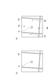
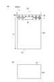
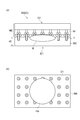
- FIG. 8 It is a figure which shows the structural example of a semiconductor device, (a) shows the schematic cross section of a logic device, (b) shows the schematic cross section of a memory device. It is a figure which shows the example of a semiconductor device, (a) shows the schematic cross section of a power device, (b) shows the bottom face of a power device. It is a figure which shows the state after thinning the board
- the inspection apparatus 1 inspects the semiconductor device D, for example, by identifying a failure location (predetermined position) in the semiconductor device D that is a device under test (DUT). It is a device for doing. More specifically, the inspection device 1 specifies a failure location and performs marking indicating the failure location around the failure location. With this marking, it is possible to easily grasp the failure location specified by the inspection apparatus 1 in the subsequent process (physical analysis) of the failure analysis.
- the semiconductor device D for example, an individual semiconductor element (discrete), an optoelectronic element, a sensor / actuator, a logic LSI (Large Scale Integration), a memory element, a linear IC (Integrated Circuit), or a hybrid device thereof.
- the individual semiconductor element includes a diode, a power transistor, and the like.
- the logic LSI is composed of a MOS (Metal-Oxide-Semiconductor) structure transistor, a bipolar structure transistor, or the like.
- the semiconductor device D may be a package including a semiconductor device, a composite substrate, or the like.
- the semiconductor device D has a substrate and a metal layer formed on the substrate.
- As the substrate of the semiconductor device D for example, a silicon substrate is used.
- the semiconductor device D is placed on the sample stage 40.
- the inspection apparatus 1 performs a failure location identifying process for identifying a failure location of the semiconductor device D and a marking process for marking the failure location around the identified failure location.
- the inspection apparatus 1 includes a stimulation apparatus 11, a light source 12, an optical system 13 including an observation optical system 13A and a marking optical system 13B, an XYZ stage 14, a photodetector 15, a laser light source 16, and a calculator 21. And a display unit 22 and an input unit 23.
- the inspection apparatus 1 includes a stimulation apparatus 11, a light source 12, an observation optical system 13A, an XYZ stage 14, a light detector 15, a computer 21, and a display unit 22 as a functional configuration related to the failure location identification process. And an input unit 23.
- the stimulation device 11 is electrically connected to the semiconductor device D via a cable and functions as a stimulation signal application unit that applies a stimulation signal to the semiconductor device D.
- the stimulation apparatus 11 is, for example, a pulse generator that applies a stimulation signal to the semiconductor device D, a tester unit that inputs a test signal, and the like.
- the stimulator 11 is operated by a power source (not shown), and repeatedly applies a stimulus signal such as a predetermined test pattern to the semiconductor device D.
- the stimulator 11 may apply a modulated current signal or may apply a direct current signal.
- the stimulation device 11 is electrically connected to the computer 21 via a cable, and applies a stimulation signal such as a test pattern designated by the computer 21 to the semiconductor device D.
- the stimulating device 11 does not necessarily have to be electrically connected to the computer 21.
- the stimulation apparatus 11 determines a stimulation signal such as a test pattern alone and applies the stimulation signal such as the test pattern to the semiconductor device D.
- the light source 12 is operated by a power source (not shown) and outputs light that illuminates the semiconductor device D.
- the light source 12 is an LED (Light Emitting Diode), a lamp light source, or the like.
- the wavelength of light output from the light source 12 is a wavelength that passes through the substrate of the semiconductor device D.
- the thickness is preferably 1064 nm or more.
- the light output from the light source 12 is guided to the observation optical system 13A.
- the observation optical system 13 ⁇ / b> A is an optical system that guides light from the substrate side of the semiconductor device D to the photodetector 15.
- the observation optical system 13A may be configured to be shared with a marking optical system 13B described later, or may be configured as a separate body from the marking optical system 13B.
- the observation optical system 13A irradiates the semiconductor device D with the light output from the light source 12 from the substrate side of the semiconductor device D, that is, the back surface D1 side of the semiconductor device D.
- the observation optical system 13A includes a beam splitter and an objective lens. The objective lens focuses the light output from the light source 12 and guided by the beam splitter onto the observation area.
- the observation optical system 13A is placed on the XYZ stage 14.
- the XYZ stage 14 is movable in the Z-axis direction and the X-axis direction and the Y-axis direction orthogonal to the Z-axis direction, where the optical axis direction of the objective lens is the Z-axis direction.
- the XYZ stage 14 is movable in the above-described three-axis directions by being controlled by a control unit 21b (described later) of the computer 21.
- the observation area is determined by the position of the XYZ stage 14.
- the observation optical system 13A transmits light (reflected light) reflected by the semiconductor device D through the substrate of the semiconductor device D and reflected by the semiconductor device D to the photodetector 15 according to the illuminated light. Specifically, the light emitted from the observation optical system 13A passes through the substrate SiE (see FIG. 4) of the semiconductor device D and is reflected by the metal layer ME (see FIG. 4). Then, the light reflected from the metal layer ME passes through the substrate SiE again and is input to the photodetector 15 via the objective lens and the beam splitter of the observation optical system 13A.
- the observation optical system 13 ⁇ / b> A transmits light emitted from the semiconductor device D to the photodetector 15 by applying a stimulus signal.
- light emission for example, emission light
- the substrate SiE passes through the objective lens and the beam splitter of the observation optical system 13A. It is input to the photodetector 15.
- the photodetector 15 captures light from the semiconductor device D and outputs image data (detection signal). For example, the photodetector 15 images the light reflected from the semiconductor device D and outputs image data for generating a pattern image. Based on the pattern image, the marking position can be grasped. The photodetector 15 captures light emitted from the semiconductor device D and outputs image data for generating a light emission image. Based on the light emission image, the light emission location in the semiconductor device D can be specified. By specifying the light emission location, the failure location of the semiconductor device D can be specified.
- a CCD (Charge Coupled Device) image sensor or a CMOS (Complementary Metal Oxide Semiconductor) image sensor capable of detecting light having a wavelength that passes through the substrate SiE of the semiconductor device D is mounted as the photodetector 15 that measures light emission.
- CMOS Complementary Metal Oxide Semiconductor
- Two-dimensional cameras such as cameras, InGaAs cameras, and MCT cameras are used.
- the computer 21 is electrically connected to the photodetector 15 and the like via a cable.
- the computer 21 is a computer including a processor (CPU: Central Processing Unit) and a storage medium such as RAM (Random Access Memory), ROM (Read Only Memory), SSD (Solid State Drive), HDD (Hard Disk Drive), and the like. It is.
- the computer 21 executes processing by the processor on the data stored in the storage medium.
- the calculator 21 generates a pattern image and a light emission image based on the image data input from the photodetector 15.
- the pattern image is an image captured so that the circuit of the semiconductor device D (such as a circuit pattern formed on the metal layer ME) can be confirmed.
- the computer 21 may be a cloud server, smart device (smartphone, tablet terminal, etc.), microcomputer, FPGA (field-programmable gate array), or the like.
- the calculator 21 acquires a pattern image of each magnification from a low magnification to a high magnification for a portion including a light emitting portion in the semiconductor device D.
- 2A shows a low-magnification pattern image A1
- FIG. 2B shows a medium-magnification pattern image A2
- FIG. 2C shows a high-magnification pattern image A3.
- the computer 21 can acquire pattern images A1 to A3 corresponding to each magnification by controlling the objective lens of the observation optical system 13A.
- FIG. 3A shows an analysis image A4 in which a high-magnification pattern image A3 and a light emission image indicating a failure location fp that is a light emission location are superimposed.
- the computer 21 outputs the analysis image A4 to the display unit 22.
- the display unit 22 is a display device such as a display for showing the analysis image A4 and the like to the user.
- the display unit 22 displays the input analysis image A4.
- the user confirms the position of the failure location fp from the analysis image A4 displayed on the display unit 22 and inputs information indicating the failure location fp to the input unit 23.
- the input unit 23 is an input device such as a keyboard and a mouse that receives input from the user.
- the input unit 23 outputs information indicating the failure location fp received from the user to the computer 21.
- the computer 21, the display unit 22, and the input unit 23 may be tablet terminals. The above is the description of the functional configuration of the inspection apparatus 1 related to the failure location specifying process.
- the marking process is a process of marking the failure location fp around the failure location fp identified by the failure location identification process.
- the inspection apparatus 1 further includes a laser light source 16 and a marking optical system 13B as a functional configuration related to the marking process, in addition to the functional configurations related to the failure location specifying process described above.
- the computer 21 includes a condition setting unit 21a, a control unit 21b (marking control unit), and an analysis unit 21c (processing unit).
- marking process laser marking is performed based on the failure location fp (predetermined position) identified in the failure location identification processing. As shown in FIGS. 3B and 4, marking locations mp are set around the failure location fp (here, 4 locations as an example).
- the laser beam output from the laser light source 16 is applied to the marking portion mp of the semiconductor device D through the marking optical system 13B. That is, laser light having a wavelength that passes through the substrate SiE is irradiated from the substrate SiE side of the semiconductor device D to the marking portion mp. Thereby, marking is formed at the boundary between the substrate SiE and the metal layer ME.
- the details of the functional configuration of the inspection apparatus 1 related to the marking process will be described.
- the condition setting unit 21a sets the marking location mp based on the information indicating the failure location fp input from the input unit 23.
- the marking locations mp are set at several locations around the specified failure location fp. The number of places is, for example, 4 places.
- the condition setting unit 21a automatically sets the marking locations mp around the failure location fp around the failure location fp.
- the marking location mp is set in a cross shape with the failure location fp as the center.
- the marking part mp may be set when the input unit 23 receives input of information indicating the marking part mp from the user who has viewed the analysis image displayed on the display unit 22.
- condition setting unit 21a sets the marking part mp based on the information indicating the marking part mp input from the input unit 23 without automatically setting the marking part mp.
- the condition setting unit 21a generates a reference image A5 (see FIG. 3B) in which a mark indicating the failure location fp and the marking location mp is added to the analysis image A4, and stores the reference image A5 in the computer 21. To do.
- the control unit 21b of the computer 21 controls the XYZ stage 14 to move the XYZ stage 14 in three axis directions. Specifically, the control unit 21b moves the XYZ stage 14 on which the marking optical system 13B is placed so that laser marking is performed at the marking location mp set by the condition setting unit 21a. When there are a plurality of marking portions mp, the control unit 21b performs control so that laser marking is sequentially performed on all the marking portions mp. That is, when the laser marking on one marking location mp is completed, the control unit 21b moves the XYZ stage 14 so that laser marking is performed on the next marking location mp. When the movement of the XYZ stage 14 is completed, the control unit 21b outputs an output start signal to the laser light source 16.
- the laser light source 16 is operated by a power source (not shown) and outputs a laser beam irradiated to the semiconductor device D.
- the laser light source 16 starts outputting laser light when an output start signal is input by the control unit 21b.
- the laser light source 16 for example, a semiconductor laser, a fiber laser, or the like can be used.
- the wavelength of the laser light output from the laser light source 16 may be in a wavelength range that transmits the substrate SiE. For example, when the substrate SiE is silicon, the wavelength is preferably 1064 nm or more.
- the marking optical system 13B irradiates the marking portion mp of the semiconductor device D with the laser light output from the laser light source 16 from the substrate SiE side of the semiconductor device D, that is, the back surface D1 side of the semiconductor device D.
- the marking optical system 13B has an objective lens.
- the objective lens focuses the laser light from the laser light source 16 on the marking location mp.
- the marking optical system 13B is placed on the XYZ stage 14.
- the XYZ stage 14 can be moved in the above-described three-axis directions by being controlled by the control unit 21b.
- the marking optical system 13B has an optical scanning unit (for example, optical scanning elements such as a galvano mirror, a polygon mirror, and a MEMS mirror) instead of the above-described XYZ stage 14 as a configuration for changing the irradiation position of the laser light.
- the control unit 21b can control the irradiation position of the laser light by controlling the operation of the optical scanning unit.
- the marking optical system 13B includes a shutter, and the shutter is operated by the control from the control unit 21b to allow the laser light from the laser light source 16 to pass or block, thereby controlling the output of the laser light. Good.
- the control unit 21b is electrically connected to the laser light source 16 and controls the irradiation of the laser light in the laser marking. Specifically, the control unit 21b controls the output of the laser light source 16 so that the marking is formed at the boundary between the substrate SiE and the metal layer ME. Preferably, the control unit 21b controls the output of the laser light source 16 so that the marking does not penetrate the metal layer ME. Thereby, the marking can be kept inside the semiconductor device D. As a result, it is possible to prevent the surface D2 of the semiconductor device D from being contaminated by debris of the semiconductor device D that may be generated at the time of marking formation. For example, the control unit 21b performs control so that the power of laser light in laser marking is 10 ⁇ J to 10 mJ.
- the control unit 21b defines the number of times (for example, 50 to 1000 shots) of irradiating the marking portion mp with the laser beam as the laser beam irradiation condition.
- the laser beam irradiation may be controlled.
- the control unit 21b defines the time for irradiating the marking portion mp with the laser light as the laser light irradiation condition. You may control irradiation of a laser beam.
- the control unit 21b outputs an output stop signal to the laser light source 16 when the laser light irradiation based on the irradiation conditions defined as described above is completed.
- the laser light source 16 stops outputting the laser light. For this reason, the laser light source 16 outputs laser light from when the output start signal is input by the control unit 21b to when the output stop signal is input.
- the marking formed by the laser beam irradiation described above may be any form that can be confirmed by the photodetector 15 or the like, and various forms are conceivable.
- the marking includes a cavity generated by laser light irradiation, an amorphous material generated by modification, and a part of the metal layer ME or substrate SiE melted by heat generated by absorbing the laser light into the metal layer ME. Can be mentioned.
- the control unit 21b performs control so as to start laser marking of the next marking portion mp after confirming that the marking is appropriately formed at the one marking portion mp. For example, the control unit 21b stops the output of the laser light source 16 after completing the laser marking (that is, laser light irradiation based on the set laser light irradiation condition) to one marking portion mp, and performs the marking.
- the optical system 13B is switched to the observation optical system 13A, and output of the light source 12 is started. Thereby, the photodetector 15 images the light from the light source 12 reflected from the semiconductor device D, and outputs the above-described image data (detection signal) to the analysis unit 21 c of the computer 21.
- the analysis unit 21c generates a pattern image based on the image data.
- a marking having an appropriate size is not formed at the marking location mp (when the marking is small)
- the intensity change of the reflected light at the marking location mp is small and the change in the optical reflection image is also small. For this reason, the influence of laser marking on the pattern image is small.
- an appropriately sized marking is formed at the marking location mp, at least one change in the refractive index, transmittance, absorptivity, and reflectance of light increases. As a result, the intensity change of the reflected light at the marking location mp increases, and a mark image indicating the marking formed at the marking location mp appears in the pattern image.
- the analysis unit 21c compares a pattern image acquired before laser marking (for example, the pattern image A3) with a pattern image acquired after laser marking, and whether or not the difference between the images is equal to or greater than a predetermined value. Determine whether. When the difference between the images is equal to or greater than the specified value (or greater than the specified value), the analysis unit 21c determines that a mark image has appeared (that is, a marking having an appropriate size has been formed). On the other hand, when the difference between the images is smaller than the specified value (or less than the specified value), the analysis unit 21c determines that the mark image does not appear (that is, the marking having an appropriate size is not formed). To do.
- the control unit 21b When it is determined by the analysis unit 21c that a mark image has appeared, the control unit 21b records that the laser marking at the marking location mp has been completed. And the control part 21b determines whether the laser marking of all the planned marking locations mp (4 locations as an example in this embodiment) was completed. When the laser marking of all the marking locations mp has been completed, the control unit 21b completes the laser marking process. On the other hand, when the marking part mp which is not marked remains, the control unit 21b controls to start laser marking of the next marking part mp.
- the control unit 21b performs control so that the laser marking at the marking location mp is executed again.
- the control unit 21b sets the irradiation condition of the laser light output from the laser light source 16 according to the size of the mark image detected by the analysis unit 21c (that is, the size of the difference between the images). May be. That is, the control unit 21b additionally calculates the irradiation amount of the laser beam necessary for forming a marking with a predetermined size according to the size of the marking that has already been formed, and according to the irradiation amount. Irradiation conditions may be set.
- the determination by the analysis unit 21c described above may be executed by a user's manual operation.
- the analysis unit 21c may determine whether or not a mark image has appeared according to the input content from the user.
- a pattern image is displayed on the display unit 22.
- information indicating whether or not a mark image appears in the pattern image is input to the input unit 23 by the user who has confirmed the pattern image by visual observation.
- the input unit 23 outputs information on whether or not a mark image appears to the computer 21.
- the analysis unit 21c determines whether or not a mark image has appeared based on information on whether or not a mark image has appeared.
- the analysis unit 21c compares the reference image A5 with the pattern image acquired after the laser marking.
- the analysis unit 21c determines that a mark formation deviation has occurred when the mark formation location in the pattern image is deviated from the marking location mp in the reference image A5.
- the correction control of the marking portion mp may be performed as follows.
- the analysis unit 21c notifies the control unit 21b of information related to mark formation displacement (such as a displacement direction and a displacement size). Then, the control unit 21b may perform position correction by moving the XYZ stage 14 so that a mark is formed at the correct marking location mp based on the information.
- the control unit 21b operates the light source 12, the observation optical system 13A, and the photodetector 15. Thereby, the photodetector 15 images the light from the light source 12 reflected from the semiconductor device D, and outputs image data (detection signal) to the analysis unit 21 c of the computer 21.
- the analysis unit 21c generates a pattern image (pattern image including a mark image) after the completion of laser marking based on the image data.
- the analysis unit 21c can generate a marking image A6 that can specify the mark image m and the failure location fp by superimposing the light emission image on the pattern image including the mark image.
- the marking image A6 is an image generated at the same magnification as the low-magnification pattern image A3.
- the analysis unit 21c can obtain marking position information indicating the relative position of each mark image m with reference to the feature point P0 of the semiconductor device D by superimposing the marking image A6 and the high-magnification pattern image A1. it can.
- the analysis unit 21c based on the image generated by superimposing the marking image A6 and the pattern image A1 as described above, each mark image m in the case where the coordinate position of the feature point P0 is the origin position. The coordinate position can be calculated.
- the laser marking is controlled so that the marking is formed at the marking portion mp, and the position of the mark image m and the position of the marking portion mp should match. Therefore, when the accuracy of the marking position by laser marking is high (when the error between the position of the mark image m and the position of the marking portion mp is small), the analysis unit 21c overlaps the pattern image A1 and the reference image A5. Based on the generated image, the coordinate position of each marking location mp when the coordinate position of the feature point P0 is the origin position may be calculated.
- the characteristic point P0 is preferably a portion showing a characteristic pattern that can be specified not only from the back surface D1 side of the semiconductor device D but also from the front surface D2 side. In this case, even when the physical analysis is performed on the semiconductor device D from the surface D2 side, the positions of the mark image m and the failure location fp can be easily specified based on the feature point P0. Examples of such a feature point P0 include a corner portion of a memory mat.
- the analysis unit 21c stores the marking position information of the mark image m (or marking portion mp) calculated as described above in a storage medium provided in the computer 21.
- the analysis unit 21c may output the marking position information to a recording medium (for example, a USB memory) that can be removed from the computer 21, or to an external computer device via a wired or wireless communication network. May be.
- the analysis unit 21 c may output marking position information to the display unit 22.
- the display unit 22 may display the marking position information as a list or may display it together with the marking image. Further, these pieces of information may be output as a paper medium by an external device such as a printer.
- the inspection apparatus 1 inspects the semiconductor device D by executing the above-described failure location specifying process, and specifies the failure location fp in the semiconductor device D (step S1). Specifically, the inspection apparatus 1 controls the XYZ stage 14 so that the visual field of the observation optical system 13A is located in an area to be observed. Then, the inspection apparatus 1 controls the XYZ stage 14 so that the objective lens is focused on the area to be observed. When the visual field of the observation optical system 13A is located in the area to be observed, the inspection apparatus 1 irradiates the semiconductor device D with the light output from the light source 12 from the back surface D1 side of the semiconductor device D by the observation optical system 13A. An optical reflection image generated by the detector 15 is acquired.
- the inspection apparatus 1 applies a stimulation signal to the semiconductor device D using the stimulation apparatus 11 and acquires a light emission image by the photodetector 15. Then, the inspection apparatus 1 generates an analysis image A4 (see (a) of FIG. 3) by superimposing the acquired optical reflection image and the light emission image, and specifies the failure location fp based on the analysis image A4.
- a marking location mp is set according to the position of the failure location fp, and a reference image A5 is generated by adding a mark indicating the failure location fp and the marking location mp to the analysis image A4.
- the control part 21b of the computer 21 moves the XYZ stage 14 to the position according to the said marking location mp.
- the marking optical system 13B placed on the XYZ stage 14 moves to an appropriate position corresponding to the marking location mp (step S2).
- control unit 21b irradiates the semiconductor device D from the substrate SiE side with a laser beam having a wavelength that transmits the substrate SiE so that the marking is formed at the boundary between the substrate SiE and the metal layer ME at the marking location mp.
- control unit 21b controls the output of the laser light source 16 on the basis of the laser beam irradiation conditions set in advance as described above, thereby executing laser beam irradiation on the marking portion mp. (Step S3).
- step S3 when the laser light irradiation based on the above-described irradiation conditions is completed, the control unit 21b stops the output of the laser light source 16, switches from the marking optical system 13B to the observation optical system 13A, and outputs the light source 12 To start.
- the photodetector 15 images the light from the light source 12 reflected from the semiconductor device D, and outputs the above-described image data (detection signal) to the analysis unit 21 c of the computer 21.
- the analysis unit 21c generates a pattern image based on the image data.
- the analysis unit 21c determines whether or not a mark image has appeared on the pattern image (step S4). If it is determined that no mark image appears on the pattern image (step S4: NO), the process of step S3 is executed again. On the other hand, when it is determined that a mark image has appeared on the pattern image (step S4: YES), the control unit 21b determines whether or not a marking portion mp where laser marking has not been performed remains (step S5). . When it is determined that the marking part mp that has not been subjected to laser marking remains (step S5: YES), the process of step S2 is performed on the remaining marking part mp. On the other hand, if it is determined that there is no remaining marking portion mp where laser marking has not been performed (that is, laser marking has been completed for all marking portions mp) (step S5: NO), the laser marking process is completed. To do.
- the analysis unit 21c records the marking position information (step S6). Specifically, the analysis unit 21c generates a marking image A6 (see FIG. 5) that is a pattern image after completion of laser marking (a pattern image including a mark image). Further, the analysis unit 21c, based on the image generated by superimposing the marking image A6 and the pattern image A1 (see FIG. 5), each mark image m when the coordinate position of the feature point P0 is the origin position. The coordinate position of is calculated. Thereby, information indicating a relative position with respect to the feature point P0 of each mark image m is obtained as marking position information for specifying the marking position. The analysis unit 21c stores the marking position information thus obtained in a storage medium provided in the computer 21.
- the analysis unit 21c outputs marking position information (step S7). Specifically, as described above, the analysis unit 21c may output the marking position information to a portable recording medium such as a USB memory, or perform an external computer device (for example, physical analysis of the semiconductor device D). For example, an analysis device to be performed).
- a portable recording medium such as a USB memory
- an external computer device for example, physical analysis of the semiconductor device D.
- an analysis device to be performed for example, an analysis device to be performed.
- FIG. 7A shows a schematic cross section of a semiconductor device 100 that is a logic device
- FIG. 7B shows a schematic cross section of a semiconductor device 200 that is a memory device
- FIG. The schematic cross section of the semiconductor device 300 which is a power device is shown.
- Each of the semiconductor devices 100, 200, 300 has a transistor layer T at the boundary between the metal layer ME and the substrate SiE.
- the transistor layer T includes a circuit element (for example, a gate element) embedded in at least one of the metal layer ME and the substrate SiE at the boundary between the metal layer ME and the substrate SiE.
- the metal layer ME includes a wiring layer provided with a wiring W that is electrically connected to the transistor layer T on the surface D2 side of the transistor layer T.
- the marking M is formed on the transistor layer T located mainly at the boundary between the substrate SiE and the wiring layer by the laser marking described above.
- FIG. 9 is a diagram illustrating a state after the substrate SiE of the semiconductor device 300 illustrated in FIG. 8 is thinned.
- the marking M is formed on the transistor layer T which is the boundary between the substrate SiE and the metal layer ME.
- the marking M can be easily confirmed from the back surface D1 side by using an electron beam (EB) or the like by cutting the substrate SiE from the back surface D1 side to make it thinner (FIG. 9). (See (b)).
- the thickness d1 of the substrate SiE before thinning is about 100 ⁇ m to 700 ⁇ m
- the thickness d2 of the substrate SiE after thinning is about 10 ⁇ m.
- the marking M may be confirmed even with visible light.
- FIG. 10 is a diagram showing an example of an SEM image showing the marking M formed between the substrate of the semiconductor device and the metal layer in the case of a flash memory (memory device) by the inspection method executed by the inspection apparatus 1.
- a of FIG. 10 is a low-magnification (magnification: 30000) image obtained by imaging a cross-sectional portion including the marking M in the semiconductor device with a scanning electron microscope (SEM).
- FIG. 10B is an image with a high magnification (magnification: 60000) obtained by imaging a cross-sectional portion including the marking M in the semiconductor device with an SEM.
- the substrate SiE is transmitted so that the marking is formed at least at the boundary between the substrate SiE and the metal layer ME based on the failure location fp (predetermined position) specified in the semiconductor device D.
- the semiconductor device D is irradiated with laser light having a wavelength to be emitted from the substrate SiE side.
- the position can be easily confirmed from either the front surface D2 side (metal layer ME side) or the back surface D1 side (substrate SiE side).
- a marking can be formed. Thereby, when laser marking is performed from the substrate SiE side of the semiconductor device D, it is possible to easily confirm the marking position from either the front surface D2 side or the back surface D1 side during physical analysis.
- control unit 21b controls the output of the laser light source 16 so that the marking does not penetrate the metal layer ME. Thereby, the marking can be kept inside the semiconductor device D. As a result, it is possible to prevent the surface D2 of the semiconductor device D from being contaminated by debris of the semiconductor device D that may be generated at the time of marking formation.
- control unit 21b controls the output of the laser light source so that at least one of cavities, reforming, and melting occurs as marking. Thereby, marking can be formed appropriately.
- the inspection apparatus 1 includes an analysis unit 21c that acquires a pattern image (for example, the above-described marking image A6) of the semiconductor device D including the mark image m indicating the marking based on the detection signal.
- a pattern image for example, the above-described marking image A6
- Such a pattern image makes it possible to easily grasp the marking position in physical analysis.
- the analysis unit 21c acquires marking position information for specifying the marking position based on the pattern image, and outputs the marking position information. Thereby, marking position information for specifying a marking position in physical analysis can be output to an external device or the like. Therefore, for example, even when the inspection apparatus 1 that performs marking and the analysis apparatus that performs physical analysis are arranged at different locations, the marking position information necessary for performing physical analysis on the analysis apparatus is appropriately obtained. Can be handed over.
- the analysis unit 21c acquires information indicating the relative position of the marking based on the feature point P0 of the semiconductor device D as marking position information. As described above, by using the relative position of the marking with respect to the position of the feature point P0 (for example, the groove portion of the wiring pattern) of the semiconductor device D as the marking position information, it is possible to accurately grasp the position of the marking.
- the marking is formed at the failure location fp of the semiconductor device D specified by inspecting the semiconductor device D, but the position where the marking is formed is not limited to the failure location fp. That is, the inspection apparatus 1 transmits the substrate SiE from the substrate SiE side to the semiconductor device D so that the marking is formed at least at the boundary between the substrate SiE and the metal layer ME with respect to a predetermined position of the semiconductor device D.
- the laser beam may be irradiated. According to such a configuration, a marking forming method for performing laser marking on the semiconductor device D having the substrate SiE and the metal layer ME formed on the substrate SiE is realized.
- the configurations of Modifications 1 to 4 described below may be employed.
- the inspection apparatus 1 may include an infrared camera as the photodetector 15 instead of the two-dimensional camera described above.
- the inspection apparatus 1 may not include the light source 12.
- the observation optical system 13A does not have to include a beam splitter.
- the infrared camera captures heat rays from the semiconductor device D and generates a measurement image.
- a heat generation point in the semiconductor device D can be specified by an infrared image corresponding to the measurement image. By specifying the heat generation location, the failure location of the semiconductor device D can be specified.
- an InSb camera or the like is used as an infrared camera.
- the heat ray is light having a wavelength of 2 ⁇ m to 10 ⁇ m.
- an image showing the radiation rate distribution of the semiconductor device D can be acquired.
- the analysis unit 21c of the computer 21 generates an infrared image based on the above-described measurement image.
- the analysis unit 21c generates a pattern image based on the detection signal.
- the analysis part 21c produces
- the process for identifying the fault location from the analysis image is the same as in the above-described embodiment.
- a first measurement image including heat generation of the semiconductor device D is acquired by an infrared camera.
- the first measurement image is generated by sending a plurality of pieces of image data continuously captured with a predetermined exposure time to the computer 21 and adding the plurality of pieces of image data in the analysis unit 21c.
- the first measurement image has both the heat generation of the semiconductor device D and the shape information of the elements forming the semiconductor device D.
- a second measurement image including only information on the shape of the element formed by the semiconductor device D is acquired by the infrared camera in a state where the application of the stimulation signal by the stimulation apparatus 11 is stopped.
- the second measurement image is also sent to the computer 21 as a plurality of image data continuously captured with a predetermined exposure time, and the analysis unit 21c stores the plurality of image data. Generated by adding.
- the second measurement image has only information on the shape of the element forming the semiconductor device D.
- fever of the semiconductor device D is produced
- the analysis unit 21c generates a second measurement image as a pattern image by using a superimposed image obtained by superimposing an infrared image on the second measurement image or the first measurement image as an analysis image.
- the process for identifying the fault location from the analysis image is the same as in the above-described embodiment.
- the observation optical system 13A transmits the heat rays from the semiconductor device D to the infrared camera.
- the infrared camera detects heat rays and outputs image data (detection signal) to the computer 21.
- the analysis unit 21c generates a pattern image based on the image data.
- the processing after generating the pattern image is the same as in the above-described embodiment.
- the inspection apparatus 1 may include a power source that is electrically connected to the semiconductor device D and applies a voltage to the semiconductor device D as the stimulation apparatus 11.
- the light output from the light source 12 may be coherent light such as laser light.
- a solid-state laser light source, a semiconductor laser light source, or the like can be used as the light source 12 that outputs coherent light.
- the light source 12 when acquiring an OBIRCH (Optical Beam Induced Resistance Change) image, an SDL (Soft Defect Localization) image, or the like outputs laser light in a wavelength band in which the semiconductor device D does not generate charges (carriers).
- OBIRCH Optical Beam Induced Resistance Change
- SDL Soft Defect Localization
- the light source 12 when the substrate SiE is made of silicon, the light source 12 outputs laser light having a wavelength band larger than 1200 nm, preferably about 1300 nm.
- the light source 12 when acquiring an OBIC image, a LADA (Laser Assisted Device Alteration) image, and the like needs to output light in a wavelength region in which the semiconductor device D generates charges (carriers).
- a laser beam having a wavelength band of about 1064 nm is output.
- the light output from the light source 12 may be incoherent (non-coherent) light.
- the observation optical system 13A includes an optical scanning unit and an objective lens.
- the optical scanning unit scans the irradiation spot on the back surface D1 of the semiconductor device D.
- the optical scanning unit is configured by optical scanning elements such as a galvano mirror, a polygon mirror, and a MEMS mirror, for example.
- the objective lens condenses the light guided by the optical scanning unit on the irradiation spot.
- the inspection apparatus 1 may include an electrical signal detector electrically connected to the semiconductor device D.
- the electric signal detector detects an electric signal generated in the semiconductor device D in response to the laser light.
- the electric signal detector outputs an electric signal characteristic value corresponding to the detected electric signal to the computer 21.
- the photodetector 15 may be comprised by the optical sensor.
- the optical sensor detects the reflected light of the semiconductor device D according to the laser light and outputs a detection signal to the computer 21.
- the optical sensor is, for example, a photodiode, an avalanche photodiode, a photomultiplier tube, or an area image sensor.
- the analysis unit 21c of the computer 21 generates an electrical signal image in which the electrical signal characteristic value is imaged in association with the scanning position of the laser beam corresponding to the optical scanning unit controlled by the control unit 21b.
- the analysis unit 21c generates an optical reflection image based on the detection signal.
- the analysis unit 21c generates a superimposed image obtained by superimposing the electric signal image on the optical reflection image as an analysis image.
- the process for identifying the fault location from the analysis image is the same as in the above-described embodiment.
- the electrical signal image is, for example, an OBIC image that is a photovoltaic current image, an OBIRCH image that is an electric quantity change image, an SDL image that is an error information image, an LADA image, or the like.
- An OBIC image is an image obtained by detecting a photocurrent generated by laser irradiation and imaging a current value or a current change value of the photocurrent as an electric signal characteristic value.
- An OBIRCH image is a change in the resistance value at the irradiation position in the semiconductor device D by irradiating the semiconductor device D with a constant current applied to the semiconductor device D, and a voltage value or a change in the voltage according to the change in the resistance value. It is the image which imaged the value as an electric signal characteristic value.
- the OBIRCH image is obtained by changing the resistance value at the irradiation position in the semiconductor device D by irradiating the semiconductor device D with a constant voltage applied thereto, and changing the current change value according to the change in the resistance value. It may be an image imaged as an electric signal characteristic value.
- the SDL image detects a malfunction state by irradiating a laser having a wavelength at which carriers are not excited while a stimulus signal such as a test pattern is applied to the semiconductor device D, and detects information related to the malfunction state (for example, a PASS / FAIL signal). Is converted into a luminance count as an electric signal characteristic value and converted into an information image.
- the LADA image is detected by detecting a malfunction state by irradiating the semiconductor device D with a laser having a wavelength that excites carriers in a state where a stimulus signal such as a test pattern is applied, and information on the malfunction state (for example, PASS / FAIL). Signal) is converted into a luminance count as an electric signal characteristic value and converted into an information image.
- a malfunction state by irradiating the semiconductor device D with a laser having a wavelength that excites carriers in a state where a stimulus signal such as a test pattern is applied, and information on the malfunction state (for example, PASS / FAIL). Signal) is converted into a luminance count as an electric signal characteristic value and converted into an information image.
- the light source 12 outputs light irradiated on the back surface D1 side of the semiconductor device D.
- the observation optical system 13A irradiates the back surface D1 of the semiconductor device D with the light output from the light source 12.
- the observation optical system 13A transmits the reflected light from the semiconductor device D according to the irradiated light to the photodetector 15 that is an optical sensor.
- the optical sensor detects reflected light and outputs a detection signal to the computer 21.
- the analysis part 21c produces
- the processing after generating the pattern image is the same as in the above-described embodiment.
- the inspection apparatus 1 may specify a failure position by an optical probing technique called EOP or EOFM (Electro-Optical Frequency Mapping).
- EOP optical probing technique
- EOFM Electro-Optical Frequency Mapping
- the light from the light source 12 is scanned by the semiconductor device D, and the reflected light from the semiconductor device D is detected by the photodetector 15 which is an optical sensor.
- the reflected light is output to the computer 21, and an optical reflection image is generated by the analysis unit 21c.
- the user selects and inputs the input from the input unit 23 based on the optical reflection image displayed on the display unit 22.
- the irradiated spot is irradiated with light output from the light source 12.
- the wavelength of the light output from the light source 12 is, for example, 530 nm or more, and preferably 1064 nm or more.
- the reflected light modulated in accordance with the operation of the element in the semiconductor device D is detected by the optical sensor and output to the computer 21 as a detection signal.
- the analysis unit 21c a signal waveform is generated based on the detection signal, and the signal waveform is displayed on the display unit 22.
- the above-described optical reflection image can be used as an analysis image by searching for a failure location from the signal waveform observed while changing the irradiation spot based on the above-described optical reflection image.
- the analysis unit 21c may generate an electro-optic frequency mapping image (EOFM image) obtained by imaging the phase difference information between the detection signal and the stimulus signal such as the test pattern in association with the irradiation position.
- EOFM image electro-optic frequency mapping image
- the phase difference information can be obtained from the AC component extracted from the detection signal.
- An optical reflection image can be obtained by imaging the DC component extracted simultaneously with the AC component in association with the irradiation position.
- a superimposed image obtained by superimposing the EOFM image on the optical reflection image can be used as the analysis image.
- the inspection apparatus 1 may specify a failure position by a magneto-optical probing technique.
- the inspection apparatus 1 includes a magneto-optical crystal (MO crystal).
- the observation optical system 13A includes a light splitting optical system.
- the magneto-optical crystal can be arbitrarily arranged with respect to the semiconductor device D.
- the magneto-optical crystal is switched to a configuration in which the magneto-optical crystal is disposed between the objective lens and the semiconductor device D, and the magneto-optical crystal is brought into contact with the semiconductor device D to which a stimulus signal such as a test pattern is applied. Then, the light from the light source 12 is irradiated onto the magneto-optical crystal through the light splitting optical system and the optical scanning unit, and the reflected light is detected by the photodetector 15 which is an optical sensor.
- the semiconductor device D when a current flows by applying a stimulus signal such as a test pattern, the surrounding magnetic field changes and the polarization state of light reflected by the magneto-optical crystal changes.
- the light whose intensity has changed in accordance with the change in the polarization state is input to the optical sensor via the light splitting optical system.
- the light whose intensity has changed in accordance with the change in the polarization state is detected by the optical sensor, and is output as a detection signal to the computer 21, thereby generating a magneto-optical image.
- a superimposed image obtained by superimposing a porcelain optical image on an optical reflection image may be used as an analysis image.
Landscapes
- Engineering & Computer Science (AREA)
- Physics & Mathematics (AREA)
- General Engineering & Computer Science (AREA)
- General Physics & Mathematics (AREA)
- Health & Medical Sciences (AREA)
- Toxicology (AREA)
- Electromagnetism (AREA)
- Computer Hardware Design (AREA)
- Microelectronics & Electronic Packaging (AREA)
- Computer Vision & Pattern Recognition (AREA)
- Testing Or Measuring Of Semiconductors Or The Like (AREA)
- Optics & Photonics (AREA)
- Tests Of Electronic Circuits (AREA)
- Manufacturing & Machinery (AREA)
- Laser Beam Processing (AREA)
- Small-Scale Networks (AREA)
- Emergency Protection Circuit Devices (AREA)
- Arrangements For Transmission Of Measured Signals (AREA)
Abstract
一実施形態に係る検査方法は、基板SiE及び基板SiE上に形成されたメタル層MEを有する半導体デバイスDにレーザマーキングを行う検査方法であって、半導体デバイスDを検査することにより、半導体デバイスDにおける故障個所fpを特定するステップと、故障個所fpに基づいて、少なくとも基板SiEとメタル層MEとの境界にマーキングが形成されるように、基板SiE側から半導体デバイスDに基板SiEを透過する波長のレーザ光を照射するステップと、を含む。
Description
本発明の一側面は、半導体デバイスの検査方法、検査装置、及びマーキング形成方法に関する。
半導体デバイスを検査する技術として、故障個所が特定された場合に、故障個所の周囲数か所に対して、レーザ光の照射によるマーキングを行う技術がある。このような技術は、故障解析における後工程において、マーキングによって故障個所を容易に把握することができることから、極めて有効な技術である。
パッケージされたサンプル(半導体デバイス)及びメタル層側に窓のないプローブカードを用いる必要があるサンプル等にマーキングを行う場合、表面側(メタル層側)からレーザ光を照射できないため、裏面側(基板側)からレーザ光を照射する必要がある。例えば特許文献1には、SiC基板を用いた半導体デバイスの故障位置をOBIRCH(Optical Beam Induced Resistance Change)法によって解析する故障解析装置が開示されている。特許文献1には、裏面側からレーザ光を照射し、基板の表面側のデバイス及び回路にレーザマーキングを行うことが開示されている。
しかしながら、特許文献1には、マーキングの詳細な位置は開示されていない。また、マーキングに基づいて半導体デバイスの物理解析を行うとき、マーキングの位置を表面側から確認する場合もあれば、裏面側から確認する場合もある。従って、マーキングが形成される位置は、表面側及び裏面側のいずれからも容易に確認可能な位置であることが好ましい。
そこで、本発明の一側面は、半導体デバイスの基板側からレーザマーキングを行う場合において、物理解析時に表面側及び裏面側のいずれからもマーキング位置を容易に確認することができる検査方法、検査装置、及びマーキング形成方法を提供することを目的とする。
本発明の一側面に係る検査方法は、基板及び基板上に形成されたメタル層を有する半導体デバイスにレーザマーキングを行う検査方法であって、半導体デバイスを検査することにより、半導体デバイスにおける所定位置を特定するステップと、所定位置に基づいて、少なくとも基板とメタル層との境界にマーキングが形成されるように、基板を透過する波長のレーザ光を基板側から半導体デバイスに照射するステップと、を含む。
この検査方法では、半導体デバイスにおいて特定された所定位置(例えば故障個所)に基づいて、少なくとも基板とメタル層との境界にマーキングが形成されるように、基板を透過する波長のレーザ光が基板側から半導体デバイスに照射される。このように、基板とメタル層との境界にマーキングを形成することにより、表面側(メタル層側)及び裏面側(基板側)のいずれからも容易に確認可能な位置にマーキングを形成することができる。これにより、半導体デバイスの基板側からレーザマーキングを行う場合において、物理解析時に表面側及び裏面側のいずれからもマーキング位置を容易に確認することが可能となる。
レーザ光を照射するステップでは、マーキングがメタル層を貫通しないように、レーザ光の照射を制御してもよい。これにより、マーキングを半導体デバイスの内部に留めることができる。その結果、マーキング形成時に生じ得る半導体デバイスの破片(デブリ)によって半導体デバイスの表面が汚染されることを防止することができる。
レーザ光を照射するステップでは、マーキングとして、空洞、改質、及び溶融のうち少なくとも1つが生じるように、レーザ光の照射を制御してもよい。これにより、マーキングを適切に形成することができる。
上記検査方法は、マーキングを示すマーク像を含む半導体デバイスのパターン画像を取得するステップを更に含んでもよい。これにより、マーキング位置を半導体デバイスのパターン(例えば配線パターン)とともに視覚的に把握可能なパターン画像を取得することができる。このようなパターン画像により、物理解析においてマーキング位置を容易に把握することが可能となる。
上記検査方法は、パターン画像に基づいて、マーキングの位置を特定する位置情報を取得するステップと、当該位置情報を出力するステップと、を更に含んでもよい。これにより、物理解析においてマーキング位置を特定するための位置情報を外部装置等に出力することができる。従って、例えばマーキングを行う検査装置と物理解析を行う解析装置とが異なる場所に配置される場合であっても、当該解析装置に対して物理解析を行うために必要な位置情報を適切に受け渡すことができる。
位置情報を取得するステップでは、半導体デバイスの特徴点の位置を基準としたマーキングの相対位置を示す情報を位置情報として取得してもよい。このように半導体デバイスの特徴点(例えば配線パターンの溝部等)の位置に対するマーキングの相対位置を位置情報として用いることで、マーキングの位置を正確に把握することが可能となる。
上記検査方法は、レーザ光を照射するステップよりも後に、基板を薄型化し、薄型化された基板側から半導体デバイスを観察するステップを更に含んでもよい。基板を薄型化することにより、上述の観察するステップにおいて、マーキングの位置を容易に確認することができる。これにより、物理解析をマーキングの位置に基づいて正確に行うことができる。
本発明の一側面に係る検査装置は、基板及び基板上に形成されたメタル層を有する半導体デバイスにレーザマーキングを行う検査装置であって、半導体デバイスの基板側からの光を伝達する観察用光学系と、観察用光学系を介して半導体デバイスからの光を検出し、検出信号を出力する光検出器と、基板を透過する波長のレーザ光を出力するレーザ光源と、レーザ光源により出力されたレーザ光を、基板側から半導体デバイスに照射するマーキング用光学系と、検出信号に基づいて特定される所定位置に基づいて、少なくとも基板とメタル層との境界にマーキングが形成されるように、レーザ光源の出力を制御するマーキング制御部と、を備える。
この検査装置では、半導体デバイスにおいて特定された所定位置(例えば故障個所)に基づいて、少なくとも基板とメタル層との境界にマーキングが形成されるように、基板を透過する波長のレーザ光が基板側から半導体デバイスに照射される。このように、基板とメタル層との境界にマーキングを形成することにより、表面側(メタル層側)及び裏面側(基板側)のいずれからも容易に確認可能な位置にマーキングを形成することができる。これにより、半導体デバイスの基板側からレーザマーキングを行う場合において、物理解析時に表面側及び裏面側のいずれからもマーキング位置を容易に確認することが可能となる。
マーキング制御部は、マーキングがメタル層を貫通しないように、レーザ光源の出力を制御してもよい。これにより、マーキングを半導体デバイスの内部に留めることができる。その結果、マーキング形成時に生じ得る半導体デバイスの破片(デブリ)によって半導体デバイスの表面が汚染されることを防止することができる。
マーキング制御部は、マーキングとして、空洞、改質、及び溶融のうち少なくとも1つが生じるように、レーザ光源の出力を制御してもよい。これにより、マーキングを適切に形成することができる。
上記検査装置は、検出信号に基づいて、マーキングを示すマーク像を含む半導体デバイスのパターン画像を取得する処理部を更に備えてもよい。これにより、マーキング位置を半導体デバイスのパターン(例えば配線パターン)とともに視覚的に把握可能なパターン画像を取得することができる。このようなパターン画像により、物理解析においてマーキング位置を容易に把握することが可能となる。
処理部は、パターン画像に基づいて、マーキングの位置を特定する位置情報を取得し、当該位置情報を出力してもよい。これにより、物理解析においてマーキング位置を特定するための位置情報を外部装置等に出力することができる。従って、例えばマーキングを行う検査装置と物理解析を行う解析装置とが異なる場所に配置される場合であっても、当該解析装置に対して物理解析を行うために必要な位置情報を適切に受け渡すことができる。
処理部は、半導体デバイスの特徴点を基準としたマーキングの相対位置を示す情報を位置情報として取得してもよい。このように半導体デバイスの特徴点(例えば配線パターンの溝部等)の位置に対するマーキングの相対位置を位置情報として用いることで、マーキングの位置を正確に把握することが可能となる。
本発明の一側面に係るマーキング形成方法は、基板及び基板上に形成されたメタル層を有する半導体デバイスにレーザマーキングを行うマーキング形成方法であって、半導体デバイスの所定位置に対して、少なくとも基板とメタル層との境界にマーキングが形成されるように、基板側から半導体デバイスに基板を透過する波長のレーザ光を照射するステップと、を含む。
このマーキング形成方法では、少なくとも基板とメタル層との境界にマーキングが形成されるように、基板を透過する波長のレーザ光が基板側から半導体デバイスに照射される。このように、基板とメタル層との境界にマーキングを形成することにより、表面側(メタル層側)及び裏面側(基板側)のいずれからも容易に確認可能な位置にマーキングを形成することができる。これにより、半導体デバイスの基板側からレーザマーキングを行う場合において、物理解析時に表面側及び裏面側のいずれからもマーキング位置を容易に確認することが可能となる。
レーザ光を照射するステップでは、マーキングがメタル層を貫通しないように、レーザ光の照射を制御してもよい。これにより、マーキングを半導体デバイスの内部に留めることができる。その結果、マーキング形成時に生じ得る半導体デバイスの破片(デブリ)によって半導体デバイスの表面が汚染されることを防止することができる。
レーザ光を照射するステップでは、マーキングとして、空洞、改質、及び溶融のうち少なくとも1つが生じるように、レーザ光の照射を制御してもよい。これにより、マーキングを適切に形成することができる。
本発明の一側面によれば、半導体デバイスの基板側からレーザマーキングを行う場合において、物理解析時に表面側及び裏面側のいずれからもマーキング位置を容易に確認することができる検査方法、検査装置、及びマーキング形成方法を提供することができる。
以下、添付図面を参照して、本発明の好適な実施形態について詳細に説明する。なお、図面の説明において同一又は相当要素には同一符号を付し、重複する説明を省略する。
図1に示されるように、本実施形態に係る検査装置1は、被検査デバイス(DUT:Device Under Test)である半導体デバイスDにおいて故障箇所(所定位置)を特定する等、半導体デバイスDを検査するための装置である。より詳細には、検査装置1は、故障個所を特定するとともに、当該故障個所の周囲に、当該故障個所を示すマーキングを行う。当該マーキングによって、故障解析の後工程(物理解析)において、検査装置1が特定した故障個所を容易に把握することができる。
半導体デバイスDとしては、例えば、個別半導体素子(ディスクリート)、オプトエレクトロニクス素子、センサ/アクチュエータ、ロジックLSI(Large Scale Integration)、メモリ素子、若しくはリニアIC(Integrated Circuit)等、又はそれらの混成デバイス等である。個別半導体素子は、ダイオード、パワートランジスタ等を含む。ロジックLSIは、MOS(Metal-Oxide-Semiconductor)構造のトランジスタ、バイポーラ構造のトランジスタ等で構成される。また、半導体デバイスDは、半導体デバイスを含むパッケージ、複合基板等であってもよい。半導体デバイスDは、基板と、基板上に形成されたメタル層とを有する。半導体デバイスDの基板としては、例えばシリコン基板が用いられる。半導体デバイスDは、サンプルステージ40に載置されている。
検査装置1は、半導体デバイスDの故障個所を特定する故障個所特定処理、及び、特定された故障個所の周囲に当該故障個所を示すマーキングを行うマーキング処理を行う。検査装置1は、刺激装置11と、光源12と、観察用光学系13A及びマーキング用光学系13Bを含む光学系13と、XYZステージ14と、光検出器15と、レーザ光源16と、計算機21と、表示部22と、入力部23と、を備えている。
まず、故障個所特定処理に係る検査装置1の機能構成について説明する。検査装置1は、故障個所特定処理に係る機能構成として、刺激装置11と、光源12と、観察用光学系13Aと、XYZステージ14と、光検出器15と、計算機21と、表示部22と、入力部23と、を備えている。
刺激装置11は、ケーブルを介して半導体デバイスDに電気的に接続され、半導体デバイスDに刺激信号を印加する刺激信号印加部として機能する。刺激装置11は、例えば、半導体デバイスDに刺激信号を加えるパルスジェネレータ、及びテスト信号を入力するテスタユニット等である。刺激装置11は、電源(図示せず)によって動作させられ、半導体デバイスDに所定のテストパターン等の刺激信号を繰り返し印加する。刺激装置11は、変調電流信号を印加するものであってもよいし、直流電流信号を印加するものであってもよい。刺激装置11は、ケーブルを介して計算機21に電気的に接続されており、計算機21から指定されたテストパターン等の刺激信号を、半導体デバイスDに印加する。なお、刺激装置11は、必ずしも計算機21に電気的に接続されていなくてもよい。刺激装置11は、計算機21に電気的に接続されていない場合には、単体でテストパターン等の刺激信号を決定し、該テストパターン等の刺激信号を半導体デバイスDに印加する。
光源12は、電源(図示せず)によって動作させられ、半導体デバイスDを照明する光を出力する。光源12は、LED(Light Emitting Diode)及びランプ光源等である。光源12から出力される光の波長は、半導体デバイスDの基板を透過する波長である。例えば半導体デバイスDの基板がシリコンである場合、好ましくは1064nm以上である。光源12から出力された光は、観察用光学系13Aに導かれる。
観察用光学系13Aは、半導体デバイスDの基板側からの光を光検出器15へ導光する光学系である。観察用光学系13Aは、後述するマーキング用光学系13Bと共用される構成であってもよいし、マーキング用光学系13Bとは別体として構成されてもよい。観察用光学系13Aは、光源12から出力された光を半導体デバイスDの基板側、すなわち半導体デバイスDの裏面D1側から半導体デバイスDに照射する。例えば、観察用光学系13Aは、ビームスプリッタ及び対物レンズを有している。対物レンズは、光源12から出力されビームスプリッタによって導かれた光を観察エリアに集光する。例えば、観察用光学系13Aは、XYZステージ14に載置されている。XYZステージ14は、対物レンズの光軸方向をZ軸方向とすると、Z軸方向、並びに、Z軸方向に直交するX軸方向及びY軸方向に移動可能とされている。XYZステージ14は、計算機21の制御部21b(後述)に制御されることにより、上述した3軸方向に移動可能とされている。XYZステージ14の位置によって観察エリアが決定する。
観察用光学系13Aは、半導体デバイスDの基板を透過し、照明された光に応じて、半導体デバイスDにおいて反射された光(反射光)を、光検出器15に伝達する。具体的には、観察用光学系13Aから照射された光は、半導体デバイスDの基板SiE(図4参照)を透過し、メタル層ME(図4参照)で反射される。そして、メタル層MEを反射した光は、再び基板SiEを透過し、観察用光学系13Aの対物レンズ及びビームスプリッタを介して光検出器15に入力される。また、観察用光学系13Aは、刺激信号の印加によって半導体デバイスDで発生した発光を光検出器15に伝達する。具体的には、刺激信号の印加によって主に半導体デバイスDのメタル層MEで発生した発光(例えば、エミッション光)が基板SiEを透過し、観察用光学系13Aの対物レンズ及びビームスプリッタを介して光検出器15に入力される。
光検出器15は、半導体デバイスDからの光を撮像し、画像データ(検出信号)を出力する。例えば、光検出器15は、半導体デバイスDから反射された光を撮像し、パターン画像を生成するための画像データを出力する。当該パターン画像に基づいて、マーキング位置を把握することができる。また、光検出器15は、半導体デバイスDからの発光を撮像し、発光画像を生成するための画像データを出力する。当該発光画像に基づいて、半導体デバイスDにおける発光箇所を特定することができる。発光箇所を特定することにより、半導体デバイスDの故障個所を特定することができる。発光を計測する光検出器15としては、例えば、半導体デバイスDの基板SiEを透過する波長の光を検出可能なCCD(Charge Coupled Device)イメージセンサ又はCMOS(Complementary Metal Oxide Semiconductor)イメージセンサを搭載したカメラ、InGaAsカメラ、及びMCTカメラ等の2次元カメラが用いられる。
計算機21は、ケーブルを介して光検出器15等に電気的に接続されている。計算機21は、例えばプロセッサ(CPU:Central Processing Unit)、並びに記憶媒体であるRAM(Random Access Memory)、ROM(Read Only Memory)、SSD(Solid State Drive)及びHDD(Hard Disk Drive)等を含むコンピュータである。計算機21は、記憶媒体に記憶されたデータに対し、プロセッサによる処理を実行する。計算機21は、光検出器15から入力された画像データに基づいて、パターン画像及び発光画像を生成する。パターン画像とは、半導体デバイスDの回路(メタル層MEに形成された回路パターン等)を確認可能なように撮像された画像である。なお、計算機21には、クラウドサーバ、スマートデバイス(スマートフォン、タブレット端末など)、マイコン、FPGA(field-programmable gate array)等が用いられてもよい。
図2に示されるように、計算機21は、半導体デバイスDにおける発光箇所を含む部分について、低倍率から高倍率までの各倍率のパターン画像を取得する。図2の(a)は低倍率のパターン画像A1を示しており、図2の(b)は中倍率のパターン画像A2を示しており、図2の(c)は高倍率のパターン画像A3を示している。例えば、計算機21は、観察用光学系13Aの対物レンズを制御することで、各倍率に応じたパターン画像A1~A3を取得することができる。
ここで、上述した発光画像だけでは、半導体デバイスDのパターン(回路パターン等)における発光位置を特定することが難しい。そこで、計算機21は、上述のように生成されたパターン画像と、半導体デバイスDからの発光に基づく発光画像とを重畳させた重畳画像を解析画像として生成する。図3の(a)は、高倍率のパターン画像A3と発光箇所である故障個所fpを示す発光画像とを重畳させた解析画像A4を示す。
計算機21は、解析画像A4を表示部22に出力する。表示部22は、ユーザに解析画像A4等を示すためのディスプレイ等の表示装置である。表示部22は、入力された解析画像A4を表示する。この場合、ユーザは、表示部22に表示された解析画像A4から故障個所fpの位置を確認し、故障個所fpを示す情報を入力部23に入力する。入力部23は、ユーザからの入力を受け付けるキーボード及びマウス等の入力装置である。入力部23は、ユーザから受け付けた、故障個所fpを示す情報を計算機21に出力する。なお、計算機21、表示部22、及び入力部23は、タブレット端末であってもよい。以上が、故障個所特定処理に係る検査装置1の機能構成についての説明である。
次に、マーキング処理に係る検査装置1の機能構成について説明する。マーキング処理は、故障個所特定処理により特定された故障個所fpの周囲に、当該故障個所fpを示すマーキングを行う処理である。
検査装置1は、マーキング処理に係る機能構成として、上述した故障個所特定処理に係る各機能構成に加えて、レーザ光源16と、マーキング用光学系13Bと、を更に備えている。また、計算機21は、条件設定部21aと、制御部21b(マーキング制御部)と、解析部21c(処理部)とを有している。
マーキング処理においては、故障個所特定処理において特定された故障個所fp(所定位置)に基づいて、レーザマーキングが行われる。図3の(b)及び図4に示されるように、故障個所fpの周囲(ここでは一例として4箇所)に、マーキング箇所mpが設定される。マーキング処理においては、レーザ光源16によって出力されたレーザ光が、マーキング用光学系13Bを介して半導体デバイスDのマーキング箇所mpに照射される。すなわち、半導体デバイスDの基板SiE側からマーキング箇所mpに対して、基板SiEを透過する波長のレーザ光が照射される。これにより、基板SiEとメタル層MEとの境界にマーキングが形成される。以下、マーキング処理に係る検査装置1の機能構成の詳細について説明する。
条件設定部21aは、入力部23から入力された故障個所fpを示す情報に基づいて、マーキング箇所mpを設定する。マーキング箇所mpは、特定された故障個所fpの周囲数か所に設定される。数か所とは例えば4箇所である。条件設定部21aは、例えば故障個所fpを示す情報が入力されると、当該故障個所fpを中心として、当該故障個所fpの周囲4箇所に、自動的にマーキング箇所mpを設定する。具体的には、例えば平面視において、故障個所fpを中心とした十字状にマーキング箇所mpが設定される。なお、マーキング箇所mpは、表示部22に表示された解析画像を見たユーザからのマーキング箇所mpを示す情報の入力を入力部23が受け付けることより設定されてもよい。この場合、条件設定部21aは、マーキング箇所mpを自動で設定することなく、入力部23から入力されるマーキング箇所mpを示す情報に基づいて、マーキング箇所mpを設定する。条件設定部21aは、故障個所fp及びマーキング箇所mpを示した目印を解析画像A4に付加したリファレンス画像A5(図3の(b)参照)を生成し、当該リファレンス画像A5を計算機21内に保存する。
計算機21の制御部21bは、XYZステージ14を制御することにより、XYZステージ14を3軸方向に移動させる。具体的には、制御部21bは、条件設定部21aにより設定されたマーキング箇所mpにレーザマーキングが行われるように、マーキング用光学系13Bを載置するXYZステージ14を移動させる。制御部21bは、マーキング箇所mpが複数ある場合には、全てのマーキング箇所mpへのレーザマーキングが順次行われるように制御する。すなわち、制御部21bは、一のマーキング箇所mpへのレーザマーキングが完了すると、次のマーキング箇所mpのレーザマーキングが行われるように、XYZステージ14を移動させる。制御部21bは、XYZステージ14の移動が完了すると、レーザ光源16に出力開始信号を出力する。
レーザ光源16は、電源(図示せず)によって動作させられ、半導体デバイスDに照射されるレーザ光を出力する。レーザ光源16は、制御部21bによって出力開始信号が入力されると、レーザ光の出力を開始する。レーザ光源16としては、例えば、半導体レーザ及びファイバレーザ等を用いることができる。レーザ光源16から出力されるレーザ光の波長は、基板SiEを透過する波長域であればよい。当該波長は、例えば基板SiEがシリコンである場合、好ましくは1064nm以上である。
マーキング用光学系13Bは、レーザ光源16が出力したレーザ光を、半導体デバイスDの基板SiE側、すなわち半導体デバイスDの裏面D1側から半導体デバイスDのマーキング箇所mpに照射する。マーキング用光学系13Bは、対物レンズを有している。対物レンズは、レーザ光源16からのレーザ光をマーキング箇所mpに集光する。マーキング用光学系13Bは、XYZステージ14に載置されている。XYZステージ14は、制御部21bに制御されることにより、上述した3軸方向に移動可能とされている。なお、マーキング用光学系13Bは、レーザ光の照射位置を変化させる構成として、上述のXYZステージ14の代わりに、光走査部(例えばガルバノミラー、ポリゴンミラー及びMEMSミラー等の光走査素子)を有してもよい。この場合、制御部21bは、当該光走査部の動作を制御することで、レーザ光の照射位置を制御することができる。また、マーキング用光学系13Bがシャッタを備え、制御部21bからの制御によってシャッタを動作させ、レーザ光源16からのレーザ光を通過させたり遮ったりすることで、レーザ光の出力を制御してもよい。
制御部21bは、レーザ光源16と電気的に接続され、レーザマーキングにおけるレーザ光の照射を制御する。具体的には、制御部21bは、マーキングが基板SiEとメタル層MEとの境界に形成されるように、レーザ光源16の出力を制御する。好ましくは、制御部21bは、マーキングがメタル層MEを貫通しないように、レーザ光源16の出力を制御する。これにより、マーキングを半導体デバイスDの内部に留めることができる。その結果、マーキング形成時に生じ得る半導体デバイスDの破片(デブリ)によって半導体デバイスDの表面D2が汚染されることを防止することができる。例えば、制御部21bは、レーザマーキングにおけるレーザ光のパワーが10μJ~10mJとなるように制御する。制御部21bは、レーザ光源16から出力されるレーザ光をパルスレーザとする場合、マーキング箇所mpにレーザパルスを照射する回数(例えば50~1000ショット等)をレーザ光の照射条件として規定することで、レーザ光の照射を制御してもよい。また、制御部21bは、レーザ光源16から出力されるレーザ光をCWレーザ(Continuous wave laser)とする場合、マーキング箇所mpにレーザ光を照射する時間をレーザ光の照射条件として規定することで、レーザ光の照射を制御してもよい。
制御部21bは、上述のように規定された照射条件に基づくレーザ光の照射を完了すると、レーザ光源16に対して出力停止信号を出力する。レーザ光源16は、出力停止信号が入力されると、レーザ光の出力を停止する。このため、レーザ光源16は、制御部21bによって出力開始信号が入力されてから出力停止信号が入力されるまでの間レーザ光を出力する。
上述のレーザ光の照射により形成されるマーキングは、光検出器15等によって確認可能なものであればよく、種々の形態が考えられる。例えば、マーキングとしては、レーザ光の照射によって生じた空洞、改質により生じたアモルファス、及びメタル層MEにレーザ光が吸収されて発生した熱によって溶融したメタル層ME又は基板SiEの一部等が挙げられる。
制御部21bは、一のマーキング箇所mpにおいてマーキングが適切に形成されたことを確認してから、次のマーキング箇所mpのレーザマーキングを開始するように制御する。例えば、制御部21bは、一のマーキング箇所mpへのレーザマーキング(すなわち、設定されたレーザ光の照射条件に基づくレーザ光の照射)が完了した後、レーザ光源16の出力を停止し、マーキング用光学系13Bから観察用光学系13Aに切り替え、光源12の出力を開始する。これにより、光検出器15は、半導体デバイスDから反射された光源12からの光を撮像し、上述の画像データ(検出信号)を計算機21の解析部21cに出力する。解析部21cは、当該画像データに基づいてパターン画像を生成する。ここで、マーキング箇所mpに適切な大きさのマーキングが形成されていない場合(マーキングが小さい場合)、マーキング箇所mpでの反射光の強度変化が小さく、光学反射像の変化も小さい。このため、パターン画像におけるレーザマーキングの影響は少ない。一方、マーキング箇所mpに適切な大きさのマーキングが形成されている場合、光の屈折率、透過率、吸収率、及び反射率の少なくとも1つの変化が大きくなる。その結果、マーキング箇所mpでの反射光の強度変化が大きくなり、パターン画像にはマーキング箇所mpに形成されたマーキングを示すマーク像が現れる。
解析部21cは、例えば、レーザマーキング前に取得されたパターン画像(例えばパターン画像A3)とレーザマーキング後に取得されたパターン画像とを比較し、画像間の差異が予め定められた規定値以上か否かを判定する。解析部21cは、画像間の差異が当該規定値以上である(或いは規定値より大きい)場合、マーク像が現れた(すなわち、適切な大きさのマーキングが形成された)と判定する。一方、解析部21cは、画像間の差異が当該規定値より小さい(或いは規定値以下である)場合、マーク像が現れていない(すなわち、適切な大きさのマーキングが形成されていない)と判定する。
解析部21cによりマーク像が現れたと判定された場合、制御部21bは、当該マーキング箇所mpにおけるレーザマーキングが完了したことを記録する。そして、制御部21bは、予定された全てのマーキング箇所mp(本実施形態では一例として4箇所)のレーザマーキングが完了したか否かを判定する。全てのマーキング箇所mpのレーザマーキングが完了している場合、制御部21bは、レーザマーキングの処理を完了する。一方、マーキングされていないマーキング箇所mpが残っている場合、制御部21bは、次のマーキング箇所mpのレーザマーキングを開始するように制御する。
一方、解析部21cによりマーク像が現れていないと判定された場合、制御部21bは、当該マーキング箇所mpにおけるレーザマーキングを再度実行するように制御する。このとき、制御部21bは、解析部21cによって検出されたマーク像の大きさ(すなわち、画像間の差異の大きさ)に応じて、レーザ光源16から出力されるレーザ光の照射条件を設定してもよい。すなわち、制御部21bは、既に形成されているマーキングの大きさに応じて、予め定められた大きさのマーキングを形成するために追加で必要レーザ光の照射量を算出し、当該照射量に応じた照射条件を設定してもよい。
なお、上述の解析部21cによる判定は、ユーザの手動操作によって実行されてもよい。例えば、解析部21cは、ユーザからの入力内容に応じて、マーク像が現れたか否かを判定してもよい。この場合、表示部22にパターン画像が表示される。そして、当該パターン画像を目視によって確認したユーザによって、パターン画像にマーク像が現れているか否かの情報が入力部23に入力される。入力部23は、マーク像が現れているか否かの情報を計算機21に出力する。解析部21cは、マーク像が現れているか否かの情報に基づいて、マーク像が現れたか否かを判定する。
また、解析部21cは、マーク像が現れたと判定した場合において、リファレンス画像A5とレーザマーキング後に取得されたパターン画像とを比較する。そして、解析部21cは、パターン画像におけるマーク形成箇所が、リファレンス画像A5におけるマーキング箇所mpからずれている場合には、マーク形成ずれが生じていると判定する。この場合、以下のようにマーキング箇所mpの修正制御が実行されてもよい。例えば、解析部21cは、マーク形成ずれに関する情報(ずれ方向及びずれの大きさ等)を制御部21bに通知する。そして、制御部21bは、当該情報に基づいて、正しいマーキング箇所mpにマークが形成されるように、XYZステージ14を移動させることで、位置修正を行ってもよい。
以上のようにして全てのマーキング箇所mpへのレーザマーキングが完了した後、制御部21bは、光源12、観察用光学系13A、及び光検出器15を動作させる。これにより、光検出器15は、半導体デバイスDから反射された光源12からの光を撮像し、画像データ(検出信号)を計算機21の解析部21cに出力する。解析部21cは、当該画像データに基づいて、レーザマーキング完了後のパターン画像(マーク像を含むパターン画像)を生成する。
図5に示されるように、解析部21cは、マーク像を含むパターン画像に発光画像を重畳することにより、マーク像m及び故障個所fpを特定可能なマーキング画像A6を生成することができる。ここで、マーキング画像A6は、低倍率のパターン画像A3と同じ倍率で生成された画像である。解析部21cは、マーキング画像A6と高倍率のパターン画像A1とを重ね合わせることで、半導体デバイスDの特徴点P0を基準とした各マーク像mの相対位置を示すマーキング位置情報を取得することができる。例えば、解析部21cは、上述のようにマーキング画像A6とパターン画像A1とを重ね合わせることで生成される画像に基づいて、特徴点P0の座標位置を原点位置とした場合における各マーク像mの座標位置を算出することができる。
なお、上述の通り、レーザマーキングはマーキング箇所mpにマーキングが形成されるように制御され、マーク像mの位置とマーキング箇所mpの位置とは一致するはずである。従って、レーザマーキングによるマーキング位置の精度が高い場合(マーク像mの位置とマーキング箇所mpの位置との誤差が少ない場合)、解析部21cは、パターン画像A1とリファレンス画像A5とを重ね合わせることで生成される画像に基づいて、特徴点P0の座標位置を原点位置とした場合における各マーキング箇所mpの座標位置を算出してもよい。
また、特徴点P0は、半導体デバイスDの裏面D1側からだけでなく、表面D2側からも特定できるような特徴的なパターンを示す箇所であることが好ましい。この場合、半導体デバイスDを表面D2側から物理解析を行う場合にも、特徴点P0に基づいてマーク像m及び故障個所fpの位置を容易に特定することが可能となる。このような特徴点P0としては、例えば、メモリマットの隅部等が挙げられる。
解析部21cは、上述のように算出されたマーク像m(或いはマーキング箇所mp)のマーキング位置情報を、計算機21が備える記憶媒体に記憶させる。なお、解析部21cは、マーキング位置情報を計算機21に対して取り外し可能な記録媒体(例えばUSBメモリ等)に出力してもよいし、有線又は無線の通信ネットワークを介して外部のコンピュータ装置に出力してもよい。また、解析部21cは、マーキング位置情報を表示部22に出力してもよい。この場合、表示部22は、マーキング位置情報をリストとして表示してもよいし、マーキング画像とともに表示してもよい。また、これらの情報は、プリンタ等の外部機器等によって紙媒体で出力されてもよい。
次に、図6を参照して、故障個所を特定してからマーキング位置情報を出力するまでの検査装置1の動作の一例について説明する。
まず、検査装置1は、上述した故障個所特定処理を実行することにより半導体デバイスDを検査し、半導体デバイスDにおける故障個所fpを特定する(ステップS1)。具体的には、検査装置1は、観察したいエリアに観察用光学系13Aの視野が位置するように、XYZステージ14を制御する。そして、検査装置1は、観察したいエリアに対物レンズの焦点が合うように、XYZステージ14を制御する。観察したいエリアに観察用光学系13Aの視野が位置したら、検査装置1は、光源12によって出力された光が観察用光学系13Aによって半導体デバイスDの裏面D1側から半導体デバイスDに照射され、光検出器15によって生成された光学反射像を取得する。続いて、検査装置1は、刺激装置11を用いて、半導体デバイスDに刺激信号を印加し、光検出器15によって発光像を取得する。そして、検査装置1は、取得された光学反射画像と発光画像を重畳して、解析画像A4(図3の(a)参照)を生成し、解析画像A4に基づき故障個所fpを特定する。
続いて、故障個所fpの位置に応じてマーキング箇所mpが設定され、故障個所fp及びマーキング箇所mpを示した目印を解析画像A4に付加したリファレンス画像A5が生成される。そして、計算機21の制御部21bは、当該マーキング箇所mpに応じた位置にXYZステージ14を移動する。これにより、XYZステージ14に載置されたマーキング用光学系13Bは、マーキング箇所mpに応じた適切な位置に移動する(ステップS2)。
続いて、制御部21bは、マーキング箇所mpにおいて、基板SiEとメタル層MEとの境界にマーキングが形成されるように、基板SiEを透過する波長のレーザ光を基板SiE側から半導体デバイスDに照射する。具体的には、制御部21bは、上述のように予め設定されたレーザ光の照射条件に基づいて、レーザ光源16の出力を制御することによって、マーキング箇所mpへのレーザ光の照射を実行する(ステップS3)。ステップS3において、上述の照射条件に基づくレーザ光の照射が完了したら、制御部21bは、レーザ光源16の出力を停止し、マーキング用光学系13Bから観察用光学系13Aに切り替え、光源12の出力を開始する。これにより、光検出器15は、半導体デバイスDから反射された光源12からの光を撮像し、上述の画像データ(検出信号)を計算機21の解析部21cに出力する。解析部21cは、当該画像データに基づいてパターン画像を生成する。
続いて、解析部21cは、パターン画像上にマーク像が現れたか否かを判定する(ステップS4)。パターン画像上にマーク像が現れていないと判定された場合(ステップS4:NO)、再度ステップS3の処理が実行される。一方、パターン画像上にマーク像が現れたと判定された場合(ステップS4:YES)、制御部21bは、レーザマーキングが行われていないマーキング箇所mpが残っているか否かを判定する(ステップS5)。レーザマーキングが行われていないマーキング箇所mpが残っていると判定された場合(ステップS5:YES)、残りのマーキング箇所mpについてステップS2の処理が実行される。一方、レーザマーキングが行われていないマーキング箇所mpが残っていない(すなわち、全てのマーキング箇所mpへのレーザマーキングが完了した)と判定された場合(ステップS5:NO)、レーザマーキングの処理を完了する。
続いて、解析部21cは、マーキング位置情報を記録する(ステップS6)。具体的には、解析部21cは、レーザマーキング完了後のパターン画像(マーク像を含むパターン画像)であるマーキング画像A6(図5参照)を生成する。また、解析部21cは、マーキング画像A6とパターン画像A1とを重ね合わせることで生成される画像(図5参照)に基づいて、特徴点P0の座標位置を原点位置とした場合における各マーク像mの座標位置を算出する。これにより、各マーク像mの特徴点P0を基準とした相対位置を示す情報が、マーキングの位置を特定するマーキング位置情報として得られる。解析部21cは、このようにして得られたマーキング位置情報を、計算機21が備える記憶媒体に記憶させる。
続いて、解析部21cは、マーキング位置情報を出力する(ステップS7)。具体的には、解析部21cは、上述したように、マーキング位置情報をUSBメモリ等の持ち運び可能な記録媒体に出力してもよいし、外部のコンピュータ装置(例えば、半導体デバイスDの物理解析を行う解析装置等)に出力してもよい。
次に、図7及び図8を参照して、半導体デバイスDの構造例と各例におけるマーキングMの形成箇所について説明する。図7の(a)は、ロジックデバイスである半導体デバイス100の概略断面を示し、図7の(b)は、メモリデバイスである半導体デバイス200の概略断面を示し、図8の(a)は、パワーデバイスである半導体デバイス300の概略断面を示す。いずれの半導体デバイス100,200,300も、メタル層MEと基板SiEとの境界において、トランジスタ層Tを有している。トランジスタ層Tは、メタル層MEと基板SiEとの境界において、少なくともメタル層ME及び基板SiEの一方に埋め込まれた回路素子(例えばゲート素子等)を含む。また、メタル層MEは、トランジスタ層Tよりも表面D2側において、トランジスタ層Tと電気的に接続される配線Wが設けられた配線層を有する。図7及び図8に示されるように、マーキングMは、上述したレーザマーキングにより、主に基板SiEと当該配線層との境界に位置するトランジスタ層Tに形成される。
ここで、図8及び図9に示されるように、レーザマーキング後の物理解析において、基板SiEを薄型化し、薄型化された基板SiE側(裏面D1側)から半導体デバイスDを観察してもよい。ここで、図9は、図8に示される半導体デバイス300の基板SiEを薄型化した後の状態を示す図である。上述のように基板SiEとメタル層MEとの境界であるトランジスタ層TにマーキングMが形成されている。このため、基板SiEを裏面D1側から削って薄型化することにより、電子ビーム(EB:electron beam)等を用いることで、裏面D1側からマーキングMを容易に確認することができる(図9の(b)参照)。これにより、物理解析をマーキングの位置に基づいて正確に行うことができる。なお、この例において、薄型化する前の基板SiEの厚さd1は100μm~700μm程度であり、薄型化した後の基板SiEの厚さd2は10μm程度である。また、基板SiEの厚さd2が1μm程度になるまで薄型化した場合、可視光でもマーキングMを確認できる可能性がある。
図10は、検査装置1により実行される検査方法によってフラッシュメモリ(メモリデバイス)である場合の半導体デバイスの基板とメタル層との間に形成されたマーキングMを示すSEM像の一例を示す図である。図10の(a)は、当該半導体デバイスにおけるマーキングMを含む断面部分を走査型電子顕微鏡(SEM:Scanning Electron Microscope)で撮像することで得られた低倍率(倍率:30000)の画像である。図10の(b)は、当該半導体デバイスにおけるマーキングMを含む断面部分をSEMで撮像することで得られた高倍率(倍率:60000)の画像である。
次に、検査装置1及び検査装置1により実行される検査方法の作用効果について説明する。
検査装置1及び上記検査方法では、半導体デバイスDにおいて特定された故障個所fp(所定位置)に基づいて、少なくとも基板SiEとメタル層MEとの境界にマーキングが形成されるように、基板SiEを透過する波長のレーザ光が基板SiE側から半導体デバイスDに照射される。このように、基板SiEとメタル層MEとの境界にマーキングを形成することにより、表面D2側(メタル層ME側)及び裏面D1側(基板SiE側)のいずれからも容易に確認可能な位置にマーキングを形成することができる。これにより、半導体デバイスDの基板SiE側からレーザマーキングを行う場合において、物理解析時に表面D2側及び裏面D1側のいずれからもマーキング位置を容易に確認することが可能となる。
また、制御部21bは、マーキングがメタル層MEを貫通しないように、レーザ光源16の出力を制御する。これにより、マーキングを半導体デバイスDの内部に留めることができる。その結果、マーキング形成時に生じ得る半導体デバイスDの破片(デブリ)によって半導体デバイスDの表面D2が汚染されることを防止することができる。また、制御部21bは、マーキングとして、空洞、改質、及び溶融のうち少なくとも1つが生じるように、レーザ光源の出力を制御する。これにより、マーキングを適切に形成することができる。
また、検査装置1は、検出信号に基づいて、マーキングを示すマーク像mを含む半導体デバイスDのパターン画像(例えば、上述のマーキング画像A6)を取得する解析部21cを備えている。これにより、マーキング位置を半導体デバイスDのパターン(例えば配線パターン)とともに視覚的に把握可能なパターン画像を取得することができる。このようなパターン画像により、物理解析においてマーキング位置を容易に把握することが可能となる。
解析部21cは、上記パターン画像に基づいて、マーキングの位置を特定するマーキング位置情報を取得し、当該マーキング位置情報を出力する。これにより、物理解析においてマーキング位置を特定するためのマーキング位置情報を外部装置等に出力することができる。従って、例えばマーキングを行う検査装置1と物理解析を行う解析装置とが異なる場所に配置される場合であっても、当該解析装置に対して物理解析を行うために必要なマーキング位置情報を適切に受け渡すことができる。
解析部21cは、半導体デバイスDの特徴点P0を基準としたマーキングの相対位置を示す情報をマーキング位置情報として取得する。このように半導体デバイスDの特徴点P0(例えば配線パターンの溝部等)の位置に対するマーキングの相対位置をマーキング位置情報として用いることで、マーキングの位置を正確に把握することが可能となる。
以上、本発明の実施形態について説明したが、本発明は上記実施形態に限定されない。例えば、上記実施形態では、半導体デバイスDを検査することにより特定された半導体デバイスDの故障個所fpにマーキングが形成されるが、マーキングが形成される位置は故障個所fpに限られない。すなわち、検査装置1は、半導体デバイスDの所定位置に対して、少なくとも基板SiEとメタル層MEとの境界にマーキングが形成されるように、基板SiE側から半導体デバイスDに基板SiEを透過する波長のレーザ光を照射してもよい。このような構成によれば、基板SiE及び基板SiE上に形成されたメタル層MEを有する半導体デバイスDにレーザマーキングを行うマーキング形成方法が実現される。また、検査装置1において、以下に述べる変形例1~変形例4の構成が採用されてもよい。
[変形例1]
検査装置1は、光検出器15として、上述した2次元カメラの代わりに赤外カメラを備えてもよい。この場合、検査装置1は、光源12を備えなくともよい。また、光源12を備えないため、観察用光学系13Aは、ビームスプリッタを備えなくともよい。赤外カメラは、半導体デバイスDからの熱線を撮像し、測定画像を生成する。当該測定画像に応じた赤外画像により、半導体デバイスDにおける発熱箇所を特定することができる。発熱箇所を特定することにより、半導体デバイスDの故障個所を特定することができる。熱線を計測する場合には、赤外カメラとしてInSbカメラ等が用いられる。なお、熱線とは、波長2μm~10μmの光である。また、半導体デバイスDからの熱線を撮像することで、半導体デバイスDの輻射率の分布を示す画像を取得することができる。
検査装置1は、光検出器15として、上述した2次元カメラの代わりに赤外カメラを備えてもよい。この場合、検査装置1は、光源12を備えなくともよい。また、光源12を備えないため、観察用光学系13Aは、ビームスプリッタを備えなくともよい。赤外カメラは、半導体デバイスDからの熱線を撮像し、測定画像を生成する。当該測定画像に応じた赤外画像により、半導体デバイスDにおける発熱箇所を特定することができる。発熱箇所を特定することにより、半導体デバイスDの故障個所を特定することができる。熱線を計測する場合には、赤外カメラとしてInSbカメラ等が用いられる。なお、熱線とは、波長2μm~10μmの光である。また、半導体デバイスDからの熱線を撮像することで、半導体デバイスDの輻射率の分布を示す画像を取得することができる。
変形例1においては、計算機21の解析部21cは、上述した測定画像に基づいて赤外画像を生成する。また、解析部21cは、検出信号に基づいてパターン像を生成する。そして、解析部21cは、パターン像に赤外画像を重畳させた重畳画像を解析画像として生成する。解析画像から故障個所を特定する処理については、上述の実施形態と同様である。
赤外カメラによって半導体デバイスDからの熱線を計測し、解析部21cにおいて赤外画像を生成する手順の詳細について説明する。まず、刺激装置11によってテストパターン等の刺激信号が印加されている状態で、赤外カメラによって半導体デバイスDの発熱を含む第1の測定画像が取得される。この第1の測定画像は、所定の露光時間で連続的に撮像された複数枚の画像データが計算機21に送られ、解析部21cにおいて当該複数枚の画像データが加算されることにより生成される。第1の測定画像は半導体デバイスDの発熱と半導体デバイスDを形成する素子の形状の情報を併せ持つ。次に、刺激装置11による刺激信号の印加が停止された状態で、赤外カメラによって半導体デバイスDの形成する素子の形状の情報のみを含む第2の測定画像が取得される。第2の測定画像も、第1の測定画像と同様に、所定の露光時間で連続的に撮像された複数枚の画像データが計算機21に送られ、解析部21cにおいて当該複数枚の画像データが加算されることにより生成される。第2の測定画像は半導体デバイスDを形成する素子の形状の情報のみを持つ。そして、解析部21cにおいて第1の測定画像から第2の測定画像を差分処理することにより、半導体デバイスDの発熱のみを含む赤外画像を生成する。解析部21cは、第2の測定画像に赤外画像を重畳させた重畳画像又は第1の測定画像を解析画像として、第2の測定画像をパターン画像として生成する。解析画像から故障個所を特定する処理については、上述の実施形態と同様である。
レーザマーキング後にマーク像の有無を確認する処理においては、観察用光学系13Aは半導体デバイスDからの熱線を赤外カメラに伝達する。赤外カメラは、熱線を検出し、画像データ(検出信号)を計算機21に出力する。そして、解析部21cは、上述したように、画像データに基づいてパターン画像を生成する。パターン画像を生成した後の処理については、上述の実施形態と同様である。
[変形例2]
検査装置1は、刺激装置11として、半導体デバイスDに電気的に接続され、半導体デバイスDに電圧を印加する電源を備えてもよい。また、光源12から出力される光は、レーザ光のようなコヒーレントな光でもよい。コヒーレントな光を出力する光源12としては、固体レーザ光源及び半導体レーザ光源等を用いることができる。OBIRCH(Optical Beam Induced Resistance Change)画像及びSDL(Soft Defect Localization)画像等を取得する場合の光源12は、半導体デバイスDが電荷(キャリア)を発生しない波長帯のレーザ光を出力する。例えば、基板SiEがシリコンを材料とするものである場合の光源12は、1200nmより大きく、好ましくは1300nm程度の波長帯のレーザ光を出力する。また、OBIC画像及びLADA(Laser Assisted Device Alteration)画像等を取得する場合の光源12は、半導体デバイスDが電荷(キャリア)を発生する波長域の光を出力する必要があるため、1200nm以下の光(例えば1064nm程度の波長帯のレーザ光)を出力する。光源12から出力される光は、インコヒーレント(非コヒーレント)な光でもよい。インコヒーレントな光を出力する光源12としては、SLD(Super Luminescent Diode)、ASE(Amplified Spontaneous Emission)、及びLED(Light Emitting Diode)等を用いることができる。光源12から出力された光は、偏光保存シングルモード光カプラ、及びプローブ光用の偏光保存シングルモード光ファイバを介して観察用光学系13Aに導かれ、半導体デバイスDに照射される。変形例2において、観察用光学系13Aは、光走査部及び対物レンズを有している。光走査部は、半導体デバイスDの裏面D1上の照射スポットを走査する。光走査部は、例えばガルバノミラー、ポリゴンミラー及びMEMSミラー等の光走査素子によって構成されている。対物レンズは、光走査部によって導かれた光を照射スポットに集光する。
検査装置1は、刺激装置11として、半導体デバイスDに電気的に接続され、半導体デバイスDに電圧を印加する電源を備えてもよい。また、光源12から出力される光は、レーザ光のようなコヒーレントな光でもよい。コヒーレントな光を出力する光源12としては、固体レーザ光源及び半導体レーザ光源等を用いることができる。OBIRCH(Optical Beam Induced Resistance Change)画像及びSDL(Soft Defect Localization)画像等を取得する場合の光源12は、半導体デバイスDが電荷(キャリア)を発生しない波長帯のレーザ光を出力する。例えば、基板SiEがシリコンを材料とするものである場合の光源12は、1200nmより大きく、好ましくは1300nm程度の波長帯のレーザ光を出力する。また、OBIC画像及びLADA(Laser Assisted Device Alteration)画像等を取得する場合の光源12は、半導体デバイスDが電荷(キャリア)を発生する波長域の光を出力する必要があるため、1200nm以下の光(例えば1064nm程度の波長帯のレーザ光)を出力する。光源12から出力される光は、インコヒーレント(非コヒーレント)な光でもよい。インコヒーレントな光を出力する光源12としては、SLD(Super Luminescent Diode)、ASE(Amplified Spontaneous Emission)、及びLED(Light Emitting Diode)等を用いることができる。光源12から出力された光は、偏光保存シングルモード光カプラ、及びプローブ光用の偏光保存シングルモード光ファイバを介して観察用光学系13Aに導かれ、半導体デバイスDに照射される。変形例2において、観察用光学系13Aは、光走査部及び対物レンズを有している。光走査部は、半導体デバイスDの裏面D1上の照射スポットを走査する。光走査部は、例えばガルバノミラー、ポリゴンミラー及びMEMSミラー等の光走査素子によって構成されている。対物レンズは、光走査部によって導かれた光を照射スポットに集光する。
変形例2において、検査装置1は、半導体デバイスDに電気的に接続された電気信号検出器を備えてもよい。電気信号検出器は、レーザ光に応じて半導体デバイスDで生じた電気信号を検出する。電気信号検出器は、検出された電気信号に応じた電気信号特性値を計算機21に出力する。また、変形例2において、光検出器15は、光センサによって構成されてもよい。光センサは、レーザ光に応じた半導体デバイスDの反射光を検出し、検出信号を計算機21に出力する。光センサは、例えば、フォトダイオード、アバランシェフォトダイオード、光電子増倍管、又はエリアイメージセンサ等である。
計算機21の解析部21cは、電気信号特性値を、制御部21bが制御する光走査部に応じたレーザ光の走査位置に関連づけて画像化した電気信号画像を生成する。また、解析部21cは、検出信号に基づいて光学反射像を生成する。そして、解析部21cは、光学反射像に電気信号画像を重畳させた重畳画像を解析画像として生成する。解析画像から故障個所を特定する処理については、上述の実施形態と同様である。
電気信号画像とは、例えば、光起電流画像であるOBIC画像、電気量変化画像であるOBIRCH画像、正誤情報画像であるSDL画像、及びLADA画像等である。OBIC画像とは、レーザ照射によって生じた光起電流を検出し、光起電流の電流値又は電流変化値を電気信号特性値として画像化した画像である。OBIRCH画像とは、半導体デバイスDに一定の電流を印加した状態でレーザ照射することにより、半導体デバイスDにおける照射位置の抵抗値を変化させ、当該抵抗値の変化に応じた電圧値又は電圧の変化値を電気信号特性値として画像化した画像である。なお、OBIRCH画像は、半導体デバイスDに一定の電圧を印加した状態でレーザ照射することにより、半導体デバイスDにおける照射位置の抵抗値を変化させ、当該抵抗値の変化に応じた電流の変化値を電気信号特性値として画像化した画像であってもよい。SDL画像は、半導体デバイスDにテストパターンなどの刺激信号を印加した状態でキャリアが励起されない波長のレーザを照射して誤動作状態を検出し、当該誤作動状態に係る情報(例えばPASS/FAIL信号)を電気信号特性値として輝度カウントに変換し、情報画像化した画像である。LADA画像は、半導体デバイスDにテストパターン等の刺激信号を印加した状態でキャリアを励起するような波長のレーザを照射して誤動作状態を検出し、当該誤作動状態に係る情報(例えばPASS/FAIL信号)を電気信号特性値として輝度カウントに変換し、情報画像化した画像である。
レーザマーキング後にマーク像の有無を確認する処理においては、光源12が、半導体デバイスDの裏面D1側に照射される光を出力する。そして、観察用光学系13Aは、光源12から出力された光を半導体デバイスDの裏面D1に照射する。観察用光学系13Aは、照射された光に応じた半導体デバイスDからの反射光を光センサである光検出器15に伝達する。光センサは、反射光を検出し検出信号を計算機21に出力する。そして、解析部21cは、検出信号に基づいて光学反射像であるパターン画像を生成する。パターン画像を生成した後の処理については、上述の実施形態と同様である。
[変形例3]
検査装置1は、EOP又はEOFM(Electro-Optical Frequency Mapping)と称される光プロービング技術により故障位置を特定してもよい。
検査装置1は、EOP又はEOFM(Electro-Optical Frequency Mapping)と称される光プロービング技術により故障位置を特定してもよい。
変形例3においては、光源12からの光が半導体デバイスDに走査され、半導体デバイスDからの反射光が光センサである光検出器15に検出される。当該反射光が計算機21に出力され、解析部21cによって光学反射像が生成される。次に、刺激装置11から半導体デバイスDに対してテストパターン等の刺激信号が繰り返し印加された状態において、表示部22に表示された光学反射像に基づきユーザが選択して入力部23により入力された照射スポットに、光源12から出力された光が照射される。光源12から出力される光の波長は、例えば530nm以上であり、好ましくは1064nm以上である。そして、半導体デバイスD内の素子の動作に伴って変調された反射光が光センサにおいて検出され、検出信号として計算機21に出力される。解析部21cでは、検出信号に基づき信号波形が生成され、表示部22に当該信号波形が表示される。そして、上述した光学反射像に基づき照射スポットを変えながら観察した当該信号波形から故障個所を探すことによって、上述した光学反射像を解析画像として用いることができる。
また、解析部21cは、検出信号とテストパターン等の刺激信号との位相差情報を、照射位置に関連づけて画像化した電気光学周波数マッピング画像(EOFM画像)を生成してもよい。この場合、位相差情報は、検出信号から抽出したAC成分から求めることができる。また、AC成分と同時に抽出したDC成分を照射位置に関連づけて画像化することにより光学反射像を得ることができる。そして、光学反射像にEOFM画像を重畳させた重畳画像を解析画像として用いることができる。
[変形例4]
検査装置1は、光磁気プロービング技術により故障位置を特定してもよい。この場合、検査装置1は、磁気光学結晶(MO結晶)を備える。また、観察用光学系13Aは、光分割光学系を備える。磁気光学結晶は、半導体デバイスDに対して任意に配置できる構成となっている。まず、検査装置1では、磁気光学結晶を対物レンズ及び半導体デバイスDの間に配置しない構成に切り替えることで、変形例2及び変形例3のように、光学反射像を生成することができる。次に、磁気光学結晶を対物レンズ及び半導体デバイスDの間に配置する構成に切り替え、テストパターン等の刺激信号が印加されている半導体デバイスDに磁気光学結晶を当接させる。そして、光源12からの光が、光分割光学系及び光走査部を介して磁気光学結晶に照射され、その反射光が光センサである光検出器15に検出される。半導体デバイスDでは、テストパターン等の刺激信号の印加によって電流が流れると、周囲の磁界が変化して磁気光学結晶で反射される光の偏光状態が変化する。偏光状態の変化に応じて強度が変化した光は、光分割光学系を介して光センサに入力される。このように、偏光状態の変化に応じて強度が変化した光が光センサによって検出され、検出信号として計算機21に出力されることにより、磁気光学画像が生成される。そして、光学反射像に磁器光学画像を重畳させた重畳画像を解析画像として用いてもよい。
検査装置1は、光磁気プロービング技術により故障位置を特定してもよい。この場合、検査装置1は、磁気光学結晶(MO結晶)を備える。また、観察用光学系13Aは、光分割光学系を備える。磁気光学結晶は、半導体デバイスDに対して任意に配置できる構成となっている。まず、検査装置1では、磁気光学結晶を対物レンズ及び半導体デバイスDの間に配置しない構成に切り替えることで、変形例2及び変形例3のように、光学反射像を生成することができる。次に、磁気光学結晶を対物レンズ及び半導体デバイスDの間に配置する構成に切り替え、テストパターン等の刺激信号が印加されている半導体デバイスDに磁気光学結晶を当接させる。そして、光源12からの光が、光分割光学系及び光走査部を介して磁気光学結晶に照射され、その反射光が光センサである光検出器15に検出される。半導体デバイスDでは、テストパターン等の刺激信号の印加によって電流が流れると、周囲の磁界が変化して磁気光学結晶で反射される光の偏光状態が変化する。偏光状態の変化に応じて強度が変化した光は、光分割光学系を介して光センサに入力される。このように、偏光状態の変化に応じて強度が変化した光が光センサによって検出され、検出信号として計算機21に出力されることにより、磁気光学画像が生成される。そして、光学反射像に磁器光学画像を重畳させた重畳画像を解析画像として用いてもよい。
1…検査装置、12…光源、13A…観察用光学系、13B…マーキング用光学系、15…光検出器、16…レーザ光源、21b…制御部(マーキング制御部)、21c…解析部(処理部)、D…半導体デバイス、ME…メタル層、SiE…基板。
Claims (16)
- 基板及び前記基板上に形成されたメタル層を有する半導体デバイスにレーザマーキングを行う検査方法であって、
前記半導体デバイスを検査することにより、前記半導体デバイスにおける所定位置を特定するステップと、
前記所定位置に基づいて、少なくとも前記基板と前記メタル層との境界にマーキングが形成されるように、前記基板側から前記半導体デバイスに前記基板を透過する波長のレーザ光を照射するステップと、
を含む、検査方法。 - 前記レーザ光を照射するステップでは、前記マーキングが前記メタル層を貫通しないように、前記レーザ光の照射を制御する、
請求項1に記載の検査方法。 - 前記レーザ光を照射するステップでは、前記マーキングとして、空洞、改質、及び溶融のうち少なくとも1つが生じるように、前記レーザ光の照射を制御する、
請求項1又は2に記載の検査方法。 - 前記マーキングを示すマーク像を含む前記半導体デバイスのパターン画像を取得するステップを更に含む、
請求項1~3のいずれか一項に記載の検査方法。 - 前記パターン画像に基づいて、前記マーキングの位置を特定する位置情報を取得するステップと、
前記位置情報を出力するステップと、
を更に含む、請求項4に記載の検査方法。 - 前記位置情報を取得するステップでは、前記半導体デバイスの特徴点を基準とした前記マーキングの相対位置を示す情報を前記位置情報として取得する、
請求項5に記載の検査方法。 - 前記レーザ光を照射するステップよりも後に、前記基板を薄型化し、薄型化された前記基板側から前記半導体デバイスを観察するステップを更に含む、
請求項1~6のいずれか一項に記載の検査方法。 - 基板及び前記基板上に形成されたメタル層を有する半導体デバイスにレーザマーキングを行う検査装置であって、
前記半導体デバイスの前記基板側からの光を伝達する観察用光学系と、
前記観察用光学系を介して前記半導体デバイスからの光を検出し、検出信号を出力する光検出器と、
前記基板を透過する波長のレーザ光を出力するレーザ光源と、
前記レーザ光源により出力された前記レーザ光を、前記基板側から前記半導体デバイスに照射するマーキング用光学系と、
前記検出信号に基づいて特定される所定位置に基づいて、少なくとも前記基板と前記メタル層との境界にマーキングが形成されるように、前記レーザ光源の出力を制御するマーキング制御部と、
を備える、検査装置。 - 前記マーキング制御部は、前記マーキングが前記メタル層を貫通しないように、前記レーザ光源の出力を制御する、
請求項8に記載の検査装置。 - 前記マーキング制御部は、前記マーキングとして、空洞、改質、及び溶融のうち少なくとも1つが生じるように、前記レーザ光源の出力を制御する、
請求項8又は9に記載の検査装置。 - 前記検出信号に基づいて、前記マーキングを示すマーク像を含む前記半導体デバイスのパターン画像を取得する処理部を更に備える、
請求項8~10のいずれか一項に記載の検査装置。 - 前記処理部は、前記パターン画像に基づいて、前記マーキングの位置を特定する位置情報を取得し、前記位置情報を出力する、
請求項11に記載の検査装置。 - 前記処理部は、前記半導体デバイスの特徴点を基準とした前記マーキングの相対位置を示す情報を前記位置情報として取得する、
請求項12に記載の検査装置。 - 基板及び前記基板上に形成されたメタル層を有する半導体デバイスにレーザマーキングを行うマーキング形成方法であって、
前記半導体デバイスの所定位置に対して、少なくとも前記基板と前記メタル層との境界にマーキングが形成されるように、前記基板側から前記半導体デバイスに前記基板を透過する波長のレーザ光を照射するステップと、
を含む、マーキング形成方法。 - 前記レーザ光を照射するステップでは、前記マーキングが前記メタル層を貫通しないように、前記レーザ光の照射を制御する、
請求項14に記載のマーキング形成方法。 - 前記レーザ光を照射するステップでは、前記マーキングとして、空洞、改質、及び溶融のうち少なくとも1つが生じるように、前記レーザ光の照射を制御する、
請求項14又は15に記載のマーキング形成方法。
Priority Applications (5)
| Application Number | Priority Date | Filing Date | Title |
|---|---|---|---|
| KR1020197010423A KR20190109380A (ko) | 2017-01-19 | 2017-10-02 | 검사 방법, 검사 장치 및 마킹 형성 방법 |
| US16/478,192 US10586743B2 (en) | 2017-01-19 | 2017-10-02 | Inspection method, inspection device, and marking forming method |
| CN201780073132.9A CN110024096B (zh) | 2017-01-19 | 2017-10-02 | 检查方法、检查装置及标记形成方法 |
| CN202310864199.1A CN116884866A (zh) | 2017-01-19 | 2017-10-02 | 检查方法、检查装置及标记形成方法 |
| US16/742,382 US10923404B2 (en) | 2017-01-19 | 2020-01-14 | Inspection method, inspection device, and marking forming method |
Applications Claiming Priority (2)
| Application Number | Priority Date | Filing Date | Title |
|---|---|---|---|
| JP2017007383A JP6865044B2 (ja) | 2017-01-19 | 2017-01-19 | 検査方法、検査装置、及びマーキング形成方法 |
| JP2017-007383 | 2017-01-19 |
Related Child Applications (2)
| Application Number | Title | Priority Date | Filing Date |
|---|---|---|---|
| US16/478,192 A-371-Of-International US10586743B2 (en) | 2017-01-19 | 2017-10-02 | Inspection method, inspection device, and marking forming method |
| US16/742,382 Continuation US10923404B2 (en) | 2017-01-19 | 2020-01-14 | Inspection method, inspection device, and marking forming method |
Publications (1)
| Publication Number | Publication Date |
|---|---|
| WO2018135044A1 true WO2018135044A1 (ja) | 2018-07-26 |
Family
ID=62908127
Family Applications (1)
| Application Number | Title | Priority Date | Filing Date |
|---|---|---|---|
| PCT/JP2017/035848 Ceased WO2018135044A1 (ja) | 2017-01-19 | 2017-10-02 | 検査方法、検査装置、及びマーキング形成方法 |
Country Status (6)
| Country | Link |
|---|---|
| US (2) | US10586743B2 (ja) |
| JP (2) | JP6865044B2 (ja) |
| KR (1) | KR20190109380A (ja) |
| CN (2) | CN116884866A (ja) |
| TW (2) | TWI802125B (ja) |
| WO (1) | WO2018135044A1 (ja) |
Families Citing this family (13)
| Publication number | Priority date | Publication date | Assignee | Title |
|---|---|---|---|---|
| JP6865044B2 (ja) * | 2017-01-19 | 2021-04-28 | 浜松ホトニクス株式会社 | 検査方法、検査装置、及びマーキング形成方法 |
| WO2020003458A1 (ja) * | 2018-06-28 | 2020-01-02 | 株式会社日立ハイテクノロジーズ | 半導体検査装置 |
| KR102773941B1 (ko) * | 2020-02-18 | 2025-02-27 | 하마마츠 포토닉스 가부시키가이샤 | 반도체 고장 해석 장치 및 반도체 고장 해석 방법 |
| US12105858B2 (en) * | 2020-03-11 | 2024-10-01 | University Of Florida Research Foundation, Incorporated | Systems and methods for laser probing for hardware trojan detection |
| KR102902404B1 (ko) | 2020-06-08 | 2025-12-22 | 하마마츠 포토닉스 가부시키가이샤 | 반도체 검사 방법 및 반도체 검사 장치 |
| TWI738568B (zh) * | 2020-11-18 | 2021-09-01 | 汎銓科技股份有限公司 | 一種故障分析用的半導體試片的製備方法 |
| JP7710326B2 (ja) * | 2021-07-12 | 2025-07-18 | Jswアクティナシステム株式会社 | レーザ照射装置、レーザ照射方法、及びプログラム |
| TWI784720B (zh) * | 2021-09-17 | 2022-11-21 | 英業達股份有限公司 | 基於電腦視覺的電磁敏感性測試方法 |
| KR102794689B1 (ko) * | 2021-12-09 | 2025-04-15 | 주식회사 탑 엔지니어링 | 검사장치 및 이를 이용한 검사방법 |
| KR102418633B1 (ko) * | 2021-12-22 | 2022-07-07 | 큐알티 주식회사 | 반도체 소자의 방사선 평가 방법, 및 반도체 소자의 방사선 평가 시스템 |
| US12322709B2 (en) * | 2022-01-19 | 2025-06-03 | Nuvoton Technology Corporation Japan | Semiconductor device and laser marking method |
| KR102441670B1 (ko) * | 2022-04-20 | 2022-09-08 | 큐알티 주식회사 | 지능형 빔 세기 계산 시스템, 및 이의 계산 방법 |
| CN118762204B (zh) * | 2024-06-20 | 2025-02-14 | 深圳点扬科技有限公司 | 一种基于红外图像的故障诊断方法 |
Citations (3)
| Publication number | Priority date | Publication date | Assignee | Title |
|---|---|---|---|---|
| JP2011200897A (ja) * | 2010-03-25 | 2011-10-13 | Sumco Corp | 半導体ウェーハの製造方法 |
| JP2013101009A (ja) * | 2011-11-08 | 2013-05-23 | Fuji Electric Co Ltd | 半導体装置の故障位置解析方法及び装置 |
| JP2016148550A (ja) * | 2015-02-10 | 2016-08-18 | 浜松ホトニクス株式会社 | 検査装置及び検査方法 |
Family Cites Families (8)
| Publication number | Priority date | Publication date | Assignee | Title |
|---|---|---|---|---|
| JP2003251937A (ja) * | 2002-03-05 | 2003-09-09 | Fuji Photo Film Co Ltd | マーキング方法、マーキング装置及び感光材料 |
| JP2004146428A (ja) | 2002-10-22 | 2004-05-20 | Renesas Technology Corp | 故障解析方法 |
| TWI276818B (en) * | 2005-05-27 | 2007-03-21 | United Microelectronics Corp | Defect detection method |
| JP2012097391A (ja) | 2010-11-05 | 2012-05-24 | Murata Mach Ltd | 紡績機 |
| US9557377B2 (en) * | 2014-03-06 | 2017-01-31 | Hamamatsu Photonics K.K. | Fault analysis apparatus and fault analysis method |
| JP6412156B2 (ja) | 2014-11-27 | 2018-10-24 | テクノクオーツ株式会社 | 管理情報を設けた製品 |
| KR20170140440A (ko) * | 2015-05-11 | 2017-12-20 | 어플라이드 머티어리얼스, 인코포레이티드 | 서모그래피 및 박막 배터리 제조 |
| JP6865044B2 (ja) * | 2017-01-19 | 2021-04-28 | 浜松ホトニクス株式会社 | 検査方法、検査装置、及びマーキング形成方法 |
-
2017
- 2017-01-19 JP JP2017007383A patent/JP6865044B2/ja active Active
- 2017-10-02 CN CN202310864199.1A patent/CN116884866A/zh active Pending
- 2017-10-02 WO PCT/JP2017/035848 patent/WO2018135044A1/ja not_active Ceased
- 2017-10-02 KR KR1020197010423A patent/KR20190109380A/ko not_active Ceased
- 2017-10-02 CN CN201780073132.9A patent/CN110024096B/zh active Active
- 2017-10-02 US US16/478,192 patent/US10586743B2/en active Active
- 2017-11-01 TW TW110145161A patent/TWI802125B/zh active
- 2017-11-01 TW TW106137701A patent/TWI746680B/zh active
-
2020
- 2020-01-14 US US16/742,382 patent/US10923404B2/en active Active
-
2021
- 2021-04-05 JP JP2021064073A patent/JP7033225B2/ja active Active
Patent Citations (3)
| Publication number | Priority date | Publication date | Assignee | Title |
|---|---|---|---|---|
| JP2011200897A (ja) * | 2010-03-25 | 2011-10-13 | Sumco Corp | 半導体ウェーハの製造方法 |
| JP2013101009A (ja) * | 2011-11-08 | 2013-05-23 | Fuji Electric Co Ltd | 半導体装置の故障位置解析方法及び装置 |
| JP2016148550A (ja) * | 2015-02-10 | 2016-08-18 | 浜松ホトニクス株式会社 | 検査装置及び検査方法 |
Also Published As
| Publication number | Publication date |
|---|---|
| JP7033225B2 (ja) | 2022-03-09 |
| CN110024096B (zh) | 2023-08-04 |
| TW202246783A (zh) | 2022-12-01 |
| US10586743B2 (en) | 2020-03-10 |
| US20200152525A1 (en) | 2020-05-14 |
| TW201828383A (zh) | 2018-08-01 |
| JP2021108383A (ja) | 2021-07-29 |
| JP2018117063A (ja) | 2018-07-26 |
| US20190371682A1 (en) | 2019-12-05 |
| KR20190109380A (ko) | 2019-09-25 |
| TWI746680B (zh) | 2021-11-21 |
| TWI802125B (zh) | 2023-05-11 |
| CN110024096A (zh) | 2019-07-16 |
| US10923404B2 (en) | 2021-02-16 |
| CN116884866A (zh) | 2023-10-13 |
| JP6865044B2 (ja) | 2021-04-28 |
Similar Documents
| Publication | Publication Date | Title |
|---|---|---|
| JP7033225B2 (ja) | 検査方法、検査装置、及びマーキング形成方法 | |
| JP5996687B2 (ja) | 検査装置及び検査方法 | |
| JP7738721B2 (ja) | 半導体故障解析装置及び半導体故障解析方法 | |
| JP6151832B2 (ja) | 検査装置及び検査方法 | |
| JPWO2016056110A1 (ja) | 解析装置及び解析方法 |
Legal Events
| Date | Code | Title | Description |
|---|---|---|---|
| 121 | Ep: the epo has been informed by wipo that ep was designated in this application |
Ref document number: 17892610 Country of ref document: EP Kind code of ref document: A1 |
|
| ENP | Entry into the national phase |
Ref document number: 20197010423 Country of ref document: KR Kind code of ref document: A |
|
| NENP | Non-entry into the national phase |
Ref country code: DE |
|
| 122 | Ep: pct application non-entry in european phase |
Ref document number: 17892610 Country of ref document: EP Kind code of ref document: A1 |