WO2018105272A1 - 光変換部材 - Google Patents
光変換部材 Download PDFInfo
- Publication number
- WO2018105272A1 WO2018105272A1 PCT/JP2017/039361 JP2017039361W WO2018105272A1 WO 2018105272 A1 WO2018105272 A1 WO 2018105272A1 JP 2017039361 W JP2017039361 W JP 2017039361W WO 2018105272 A1 WO2018105272 A1 WO 2018105272A1
- Authority
- WO
- WIPO (PCT)
- Prior art keywords
- light
- gas barrier
- light conversion
- base material
- conversion film
- Prior art date
- Legal status (The legal status is an assumption and is not a legal conclusion. Google has not performed a legal analysis and makes no representation as to the accuracy of the status listed.)
- Ceased
Links
Images


Classifications
-
- H—ELECTRICITY
- H10—SEMICONDUCTOR DEVICES; ELECTRIC SOLID-STATE DEVICES NOT OTHERWISE PROVIDED FOR
- H10H—INORGANIC LIGHT-EMITTING SEMICONDUCTOR DEVICES HAVING POTENTIAL BARRIERS
- H10H20/00—Individual inorganic light-emitting semiconductor devices having potential barriers, e.g. light-emitting diodes [LED]
- H10H20/80—Constructional details
- H10H20/85—Packages
- H10H20/851—Wavelength conversion means
- H10H20/8514—Wavelength conversion means characterised by their shape, e.g. plate or foil
-
- B—PERFORMING OPERATIONS; TRANSPORTING
- B32—LAYERED PRODUCTS
- B32B—LAYERED PRODUCTS, i.e. PRODUCTS BUILT-UP OF STRATA OF FLAT OR NON-FLAT, e.g. CELLULAR OR HONEYCOMB, FORM
- B32B7/00—Layered products characterised by the relation between layers; Layered products characterised by the relative orientation of features between layers, or by the relative values of a measurable parameter between layers, i.e. products comprising layers having different physical, chemical or physicochemical properties; Layered products characterised by the interconnection of layers
- B32B7/02—Physical, chemical or physicochemical properties
-
- G—PHYSICS
- G02—OPTICS
- G02B—OPTICAL ELEMENTS, SYSTEMS OR APPARATUS
- G02B5/00—Optical elements other than lenses
- G02B5/20—Filters
-
- G—PHYSICS
- G02—OPTICS
- G02F—OPTICAL DEVICES OR ARRANGEMENTS FOR THE CONTROL OF LIGHT BY MODIFICATION OF THE OPTICAL PROPERTIES OF THE MEDIA OF THE ELEMENTS INVOLVED THEREIN; NON-LINEAR OPTICS; FREQUENCY-CHANGING OF LIGHT; OPTICAL LOGIC ELEMENTS; OPTICAL ANALOGUE/DIGITAL CONVERTERS
- G02F1/00—Devices or arrangements for the control of the intensity, colour, phase, polarisation or direction of light arriving from an independent light source, e.g. switching, gating or modulating; Non-linear optics
- G02F1/01—Devices or arrangements for the control of the intensity, colour, phase, polarisation or direction of light arriving from an independent light source, e.g. switching, gating or modulating; Non-linear optics for the control of the intensity, phase, polarisation or colour
- G02F1/13—Devices or arrangements for the control of the intensity, colour, phase, polarisation or direction of light arriving from an independent light source, e.g. switching, gating or modulating; Non-linear optics for the control of the intensity, phase, polarisation or colour based on liquid crystals, e.g. single liquid crystal display cells
- G02F1/133—Constructional arrangements; Operation of liquid crystal cells; Circuit arrangements
- G02F1/1333—Constructional arrangements; Manufacturing methods
- G02F1/1335—Structural association of cells with optical devices, e.g. polarisers or reflectors
-
- G—PHYSICS
- G02—OPTICS
- G02F—OPTICAL DEVICES OR ARRANGEMENTS FOR THE CONTROL OF LIGHT BY MODIFICATION OF THE OPTICAL PROPERTIES OF THE MEDIA OF THE ELEMENTS INVOLVED THEREIN; NON-LINEAR OPTICS; FREQUENCY-CHANGING OF LIGHT; OPTICAL LOGIC ELEMENTS; OPTICAL ANALOGUE/DIGITAL CONVERTERS
- G02F1/00—Devices or arrangements for the control of the intensity, colour, phase, polarisation or direction of light arriving from an independent light source, e.g. switching, gating or modulating; Non-linear optics
- G02F1/01—Devices or arrangements for the control of the intensity, colour, phase, polarisation or direction of light arriving from an independent light source, e.g. switching, gating or modulating; Non-linear optics for the control of the intensity, phase, polarisation or colour
- G02F1/13—Devices or arrangements for the control of the intensity, colour, phase, polarisation or direction of light arriving from an independent light source, e.g. switching, gating or modulating; Non-linear optics for the control of the intensity, phase, polarisation or colour based on liquid crystals, e.g. single liquid crystal display cells
- G02F1/133—Constructional arrangements; Operation of liquid crystal cells; Circuit arrangements
- G02F1/1333—Constructional arrangements; Manufacturing methods
- G02F1/1335—Structural association of cells with optical devices, e.g. polarisers or reflectors
- G02F1/1336—Illuminating devices
- G02F1/133621—Illuminating devices providing coloured light
-
- H—ELECTRICITY
- H10—SEMICONDUCTOR DEVICES; ELECTRIC SOLID-STATE DEVICES NOT OTHERWISE PROVIDED FOR
- H10H—INORGANIC LIGHT-EMITTING SEMICONDUCTOR DEVICES HAVING POTENTIAL BARRIERS
- H10H20/00—Individual inorganic light-emitting semiconductor devices having potential barriers, e.g. light-emitting diodes [LED]
- H10H20/80—Constructional details
- H10H20/85—Packages
- H10H20/851—Wavelength conversion means
-
- H—ELECTRICITY
- H10—SEMICONDUCTOR DEVICES; ELECTRIC SOLID-STATE DEVICES NOT OTHERWISE PROVIDED FOR
- H10H—INORGANIC LIGHT-EMITTING SEMICONDUCTOR DEVICES HAVING POTENTIAL BARRIERS
- H10H20/00—Individual inorganic light-emitting semiconductor devices having potential barriers, e.g. light-emitting diodes [LED]
- H10H20/80—Constructional details
- H10H20/85—Packages
- H10H20/851—Wavelength conversion means
- H10H20/8515—Wavelength conversion means not being in contact with the bodies
-
- C—CHEMISTRY; METALLURGY
- C09—DYES; PAINTS; POLISHES; NATURAL RESINS; ADHESIVES; COMPOSITIONS NOT OTHERWISE PROVIDED FOR; APPLICATIONS OF MATERIALS NOT OTHERWISE PROVIDED FOR
- C09K—MATERIALS FOR MISCELLANEOUS APPLICATIONS, NOT PROVIDED FOR ELSEWHERE
- C09K2323/00—Functional layers of liquid crystal optical display excluding electroactive liquid crystal layer characterised by chemical composition
- C09K2323/03—Viewing layer characterised by chemical composition
- C09K2323/031—Polarizer or dye
-
- G—PHYSICS
- G02—OPTICS
- G02F—OPTICAL DEVICES OR ARRANGEMENTS FOR THE CONTROL OF LIGHT BY MODIFICATION OF THE OPTICAL PROPERTIES OF THE MEDIA OF THE ELEMENTS INVOLVED THEREIN; NON-LINEAR OPTICS; FREQUENCY-CHANGING OF LIGHT; OPTICAL LOGIC ELEMENTS; OPTICAL ANALOGUE/DIGITAL CONVERTERS
- G02F1/00—Devices or arrangements for the control of the intensity, colour, phase, polarisation or direction of light arriving from an independent light source, e.g. switching, gating or modulating; Non-linear optics
- G02F1/01—Devices or arrangements for the control of the intensity, colour, phase, polarisation or direction of light arriving from an independent light source, e.g. switching, gating or modulating; Non-linear optics for the control of the intensity, phase, polarisation or colour
- G02F1/13—Devices or arrangements for the control of the intensity, colour, phase, polarisation or direction of light arriving from an independent light source, e.g. switching, gating or modulating; Non-linear optics for the control of the intensity, phase, polarisation or colour based on liquid crystals, e.g. single liquid crystal display cells
- G02F1/133—Constructional arrangements; Operation of liquid crystal cells; Circuit arrangements
- G02F1/1333—Constructional arrangements; Manufacturing methods
- G02F1/1335—Structural association of cells with optical devices, e.g. polarisers or reflectors
- G02F1/1336—Illuminating devices
- G02F1/133614—Illuminating devices using photoluminescence, e.g. phosphors illuminated by UV or blue light
-
- G—PHYSICS
- G02—OPTICS
- G02F—OPTICAL DEVICES OR ARRANGEMENTS FOR THE CONTROL OF LIGHT BY MODIFICATION OF THE OPTICAL PROPERTIES OF THE MEDIA OF THE ELEMENTS INVOLVED THEREIN; NON-LINEAR OPTICS; FREQUENCY-CHANGING OF LIGHT; OPTICAL LOGIC ELEMENTS; OPTICAL ANALOGUE/DIGITAL CONVERTERS
- G02F2201/00—Constructional arrangements not provided for in groups G02F1/00 - G02F7/00
- G02F2201/50—Protective arrangements
- G02F2201/501—Blocking layers, e.g. against migration of ions
-
- G—PHYSICS
- G02—OPTICS
- G02F—OPTICAL DEVICES OR ARRANGEMENTS FOR THE CONTROL OF LIGHT BY MODIFICATION OF THE OPTICAL PROPERTIES OF THE MEDIA OF THE ELEMENTS INVOLVED THEREIN; NON-LINEAR OPTICS; FREQUENCY-CHANGING OF LIGHT; OPTICAL LOGIC ELEMENTS; OPTICAL ANALOGUE/DIGITAL CONVERTERS
- G02F2202/00—Materials and properties
- G02F2202/36—Micro- or nanomaterials
-
- H—ELECTRICITY
- H10—SEMICONDUCTOR DEVICES; ELECTRIC SOLID-STATE DEVICES NOT OTHERWISE PROVIDED FOR
- H10H—INORGANIC LIGHT-EMITTING SEMICONDUCTOR DEVICES HAVING POTENTIAL BARRIERS
- H10H20/00—Individual inorganic light-emitting semiconductor devices having potential barriers, e.g. light-emitting diodes [LED]
- H10H20/80—Constructional details
- H10H20/85—Packages
- H10H20/851—Wavelength conversion means
- H10H20/8511—Wavelength conversion means characterised by their material, e.g. binder
-
- H—ELECTRICITY
- H10—SEMICONDUCTOR DEVICES; ELECTRIC SOLID-STATE DEVICES NOT OTHERWISE PROVIDED FOR
- H10H—INORGANIC LIGHT-EMITTING SEMICONDUCTOR DEVICES HAVING POTENTIAL BARRIERS
- H10H20/00—Individual inorganic light-emitting semiconductor devices having potential barriers, e.g. light-emitting diodes [LED]
- H10H20/80—Constructional details
- H10H20/85—Packages
- H10H20/851—Wavelength conversion means
- H10H20/8511—Wavelength conversion means characterised by their material, e.g. binder
- H10H20/8512—Wavelength conversion materials
-
- H—ELECTRICITY
- H10—SEMICONDUCTOR DEVICES; ELECTRIC SOLID-STATE DEVICES NOT OTHERWISE PROVIDED FOR
- H10H—INORGANIC LIGHT-EMITTING SEMICONDUCTOR DEVICES HAVING POTENTIAL BARRIERS
- H10H20/00—Individual inorganic light-emitting semiconductor devices having potential barriers, e.g. light-emitting diodes [LED]
- H10H20/80—Constructional details
- H10H20/85—Packages
- H10H20/851—Wavelength conversion means
- H10H20/8511—Wavelength conversion means characterised by their material, e.g. binder
- H10H20/8512—Wavelength conversion materials
- H10H20/8513—Wavelength conversion materials having two or more wavelength conversion materials
Definitions
- the present invention relates to a light conversion member having a barrier film, and relates to a light conversion member that increases light transmittance and increases the amount of light output.
- the present invention further relates to a display device including the light conversion member having the barrier film.
- quantum dots have attracted attention as light conversion materials.
- blue light is incident on the light conversion film including quantum dots from the backlight, the light is converted into red light and green light and emitted by two types of quantum dots having different sizes.
- an RGB light source having a sharp peak can be created together with blue light passing through without being converted, and the color gamut can be greatly expanded.
- the quantum dot has a problem that when it comes into contact with moisture or oxygen, the light emission intensity decreases due to a photo-oxidation reaction.
- Patent Document 1 describes a configuration in which a barrier film is laminated and bonded to a light conversion film containing quantum dots in order to protect the quantum dots from moisture and oxygen.
- the broken line is the light transmittance of the base material alone and the barrier layer combined with the barrier layer unplanned
- the solid line is the light transmittance of the base material before the barrier layer is formed.
- the light wavelength range from around 450 nm to around 750 nm, it is shown that the light transmittance of the combination of the base material alone and the barrier layer is lower than the light transmittance of the base material alone. Yes.
- an object of the present invention is to provide a light conversion member that can obtain high output luminance even when a barrier layer is formed.
- the present invention provides a light conversion film that converts a light color from a predetermined color, and a surface on which light to be converted of the light conversion film is incident, and moisture to the light conversion film
- a first gas barrier portion comprising one or more gas barrier layers for preventing gas intrusion, and a surface opposite to the surface of the first gas barrier portion on which the light conversion film is located, transmitting light
- a first base material that holds the conversion film and the first gas barrier unit, and the first base material has a light transmittance higher than that of the first base material with respect to the light of the predetermined color.
- the present invention provides a light conversion member using the first gas barrier part, which has a characteristic that the light transmittance of a combination of both a base material and the first gas barrier part is higher.
- the light transmittance of a combination of both the first base material and the first gas barrier portion is higher than the light transmittance of the first base material.
- a second gas barrier portion which is located on a surface side where the converted light of the light conversion film is output and includes one or more gas barrier layers which prevent moisture and gas from entering the light conversion film.
- a second base material that is located on the opposite side of the surface of the second gas barrier section where the light conversion film is located, transmits light, and holds the light conversion film and the second gas barrier section.
- the second gas barrier part having a characteristic of higher light transmittance may be used.
- the drop in the amount of light can be minimized, and higher output luminance can be obtained.
- the light conversion film may be a resin containing quantum dots or phosphors, and the predetermined color light may be blue.
- the light conversion member of the present invention may be used for a display.
- a high output luminance can be obtained by using the light conversion member of the present invention for a display.
- (A) is a figure explaining schematic structure of the light conversion member in Example 1 of this invention
- (B) is a figure explaining schematic structure of the light conversion member in Example 2 of this invention. It is the graph which showed the light transmittance of the thing which combined the light transmittance of the conventional base material single-piece
- FIG. 1A is a diagram illustrating a schematic configuration of a light conversion member in Embodiment 1 of the present invention.
- the light conversion member 3 converts light of a predetermined color of incident light 1 and outputs it as output light 2, and a light conversion film on the incident light 1 side.
- 4 is provided with a gas barrier part 5 composed of one or more gas barrier layers that prevent moisture and gas from entering the gas 4, and a substrate 6 that holds the gas barrier part 5 with the light conversion film 4 on the incident light 1 side of the gas barrier part 5. .
- the light conversion film 4 includes quantum dots and phosphors, and converts blue light into red and green light, for example. However, since the light conversion rate decreases due to the ingress of moisture or gas, the gas barrier unit 5 blocks the light.
- the gas barrier layer constituting the gas barrier unit 5 is made of an inorganic material that transmits light, such as SiCN or SiO2.
- a layer (intermediate layer) having the property of improving the smoothness of the laminated surface and increasing the adhesion between the gas barrier layers may be provided.
- the gas barrier including the intermediate layer is also provided. Define as layer.
- each gas barrier layer may be different or the same.
- the thicknesses of the gas barrier layers may be different or the same.
- the gas barrier layer constituting the gas barrier unit 5 may be one or more layers, and the number of stacked layers is not particular.
- the gas barrier 5 on the incident light 1 side has a characteristic that makes the light transmittance of a predetermined color as shown in FIG. 3 stand out so as to have a distribution with a larger peak than the light transmittance of other colors. It is desirable that the gas barrier unit 5 is composed of two or more gas barrier layers.
- the base 6 is preferably a highly transparent film.
- it may be a film such as PEN or PET, or may be different.
- the gas barrier unit 5 is configured so that the light transmittance of a combination of both the base material 6 and the gas barrier unit 5 with respect to blue light (wavelength) is higher than the light transmittance of the base material 6 alone.
- the gas barrier layer forming the portion 5 is adjusted.
- the light transmittance of a combination of both the light transmittance of the substrate 6 alone and the gas barrier portion 5 in which the gas barrier layer constituting the gas barrier portion 5 is not adjusted Is shown in FIG.
- Table 1 shows the structure of the gas barrier layer constituting the base material and the gas barrier part used in FIG.
- the gas barrier layers 1 to 6 are formed in numerical order arrangement, and the gas barrier layer 6 is closer to the substrate.
- the gas barrier unit 5 used in the present invention has a light transmittance of a combination of both the base material 6 and the gas barrier unit 5 with respect to light (wavelength) of a predetermined color.
- the thickness of the gas barrier layer is adjusted by selecting the optical refractive index of the gas barrier layer forming the gas barrier unit 5 so as to be higher than the transmittance.
- the light transmittance combining the base material 6 and the gas barrier unit 5 is higher than the light transmittance of the base material 6 alone, the light transmittance is higher than that of increasing the transmittance of the entire visible light. Can be obtained and the effect can be increased.
- the gas barrier portion may be formed so that there is a peak in transmittance according to the color of the incident light.
- An example is shown in FIG.
- the broken line indicates that the light transmittance of the combination of the base material alone and the gas barrier layer is maximized with respect to the light transmittance of other colors with respect to light having a wavelength near 400 nm (blue light). It is the base material in which the gas barrier layer was formed, and the solid line is the base material before forming the gas barrier layer.
- Table 2 shows the structure of the gas barrier layer constituting the base material and the gas barrier part used in FIG.
- the gas barrier layer 6 is formed in the numerical order arrangement of the gas barrier layer 1 to the gas barrier layer 6, and the one closer to the substrate is the gas barrier layer 6.
- the gas barrier portion 5 By using the gas barrier portion 5 with the gas barrier layer adjusted, it is possible to increase the light transmittance of the base material 6 and the gas barrier portion 5 combined with each other than the light transmittance of the base material 6 alone for a predetermined color.
- the light transmittance of a combination of both the base material 6 and the gas barrier unit 5 is higher than the light transmittance of the base material 6 alone for light of a predetermined color.
- the gas barrier unit 5 having the characteristics, even with the same amount of incident light 1, the amount of light converted to reach the light conversion film 4 compared to the case where the base material 6 alone is used without using the gas barrier unit 5.
- the amount of light after conversion by the light conversion film 4 increases, and a high output luminance can be obtained. Further, in the case of the same output luminance as the conventional one, power consumption is reduced.
- FIG. 1B is a diagram illustrating a schematic configuration of the light conversion member according to the second embodiment of the present invention.
- the light conversion member 3 converts light of a predetermined color of incident light 1 and outputs it as output light 2, and a light conversion film on the incident light 1 side.
- 4 is provided with a gas barrier part 5 composed of one or more gas barrier layers that prevent moisture and gas from entering the gas 4, and a substrate 6 that holds the gas barrier part 5 with the light conversion film 4 on the incident light 1 side of the gas barrier part 5.
- a gas barrier portion 7 composed of one or more gas barrier layers for preventing moisture and gas from entering the light conversion film 4, and a light conversion film on the output side of the light conversion film 4.
- 4 is provided with a base material 8 that holds the gas barrier section 7.
- the light conversion film 4 includes quantum dots, phosphors, and the like as in Example 1, and converts blue light into red, green, and blue light, for example. However, since the light conversion rate decreases due to the ingress of moisture or gas, it is blocked by the gas barrier unit 5 and the gas barrier unit 7.
- the gas barrier layer constituting the gas barrier unit 5 and the gas barrier unit 7 is made of an inorganic material that transmits light, such as SiCN and SiO 2, as in the first embodiment.
- a layer (intermediate layer) having the property of improving the smoothness of the laminated surface and increasing the adhesion between the gas barrier layers may be provided.
- the gas barrier including the intermediate layer is also provided. Define as layer.
- each gas barrier layer may be different or the same.
- the thicknesses of the gas barrier layers may be different or the same.
- the gas barrier layer constituting the gas barrier unit 5 may be one or more layers, and the number of stacked layers is not particular.
- the gas barrier section 5 on the incident light 1 side has a characteristic that makes the light transmittance of a predetermined color as shown in FIG. 3 stand out so as to have a distribution with a larger peak than the light transmittance of other colors.
- the gas barrier unit 5 is composed of two or more barrier layers.
- the base material 6 and the base material 8 are desirably films with high transparency.
- it may be a film such as PEN or PET, or may be different.
- the base material 6 and the base material 8 may be the same or different in material or thickness.
- the light transmittance of a combination of both the substrate 6 and the gas barrier unit 5 with respect to light (wavelength) of a predetermined color is higher than the light transmittance of the substrate 6 alone.
- the thickness of the gas barrier layer is adjusted by selecting the optical refractive index of the gas barrier layer that forms the gas barrier unit 5 so as to be higher.
- the gas barrier unit 7 used in the present invention has a light transmittance of a combination of both the base material 8 and the gas barrier unit 7 for at least red, green, and blue light (wavelengths).
- the thickness of the gas barrier layer is adjusted by selecting the optical refractive index of the gas barrier layer forming the gas barrier unit 7 so as to be higher than the ratio.
- FIG. 4 shows an example using the gas barrier unit 7 with adjusted layers.
- the broken line is a base material on which the gas barrier layer is formed so that the light transmittance of the combination of the base material and the gas barrier layer is higher than the light transmittance of the base material alone in the visible light range.
- the solid line is the base material alone before forming the gas barrier layer.
- Table 3 shows the structure of the gas barrier layer constituting the base material and the gas barrier part used in FIG.
- the gas barrier layers 1 to 6 are formed in the numerical order arrangement, and the gas barrier layer 6 is closer to the base material.
- the light transmittance of the base material 8 and the gas barrier portion 7 combined is higher than the light transmittance of the base material 8 alone with respect to visible light.
- this light conversion member 3 By using this light conversion member 3, compared with the case where the substrate 6 is used alone without using this light conversion member 3, even with the same amount of incident light 1, the predetermined light reaching the light conversion film 4 can be obtained. As the amount of light increases, the amount of light after conversion by the light conversion film 4 also increases. Further, since the light transmittance on the output side is also increased, the light quantity of the output light 2 is further increased, and a higher output luminance can be obtained. Further, in the case of the same output luminance as the conventional one, the power consumption is further reduced.
- Example 2 when using blue light that highlights the wavelength range of blue light emitted from a blue LED or the like as incident light 1 and using a light conversion film including quantum dots as the light conversion film 4,
- the gas barrier unit 7 on the output side has a higher light transmittance of a combination of both the base material 8 and the gas barrier unit 7 than the light transmittance of the base material 8 alone. It is more effective to use the gas barrier portion 7 which is a feature.
- the light conversion film including the quantum dots converts the blue light emitted from the blue LED or the like into red and green light that emphasizes the wavelength range of each color light. It is desirable that the light transmittance combining both 8 has a characteristic in which the light peaks. As a result, red, green, and blue light with higher luminance can be output by the light conversion film 4.
- Example 2 when the incident light 1 is blue light emitted from a blue LED or the like, and the light conversion film 4 is a light transmission film including a yellow phosphor that converts blue light into white light.
- the light transmittance of a combination of both the base material 8 and the gas barrier section 7 is more balanced than the light transmittance of the base material 8 alone as shown in FIG. It is more effective to use the gas barrier unit 7 characterized by being high.
- the light conversion member of the present invention may be used for a display.
- the light conversion member of the present invention is not limited to the form described above, but may be other forms within the scope of the present invention.
- the predetermined color of the present invention may include other than the visible light range such as ultraviolet.
Landscapes
- Physics & Mathematics (AREA)
- Nonlinear Science (AREA)
- General Physics & Mathematics (AREA)
- Optics & Photonics (AREA)
- Mathematical Physics (AREA)
- Chemical & Material Sciences (AREA)
- Crystallography & Structural Chemistry (AREA)
- Optical Filters (AREA)
- Laminated Bodies (AREA)
- Liquid Crystal (AREA)
- Led Device Packages (AREA)
Abstract
バリア層を形成しても、高い出力輝度を得ることができる光変換部材を提供する。具体的には、光の色を所定の色から変換する光変換膜と、光変換膜の変換する光が入射する面側に位置し、光変換膜への水分、ガスの浸入を防ぐ一層以上のガスバリア層からなる第1のガスバリア部と、第1のガスバリア部の光変換膜が位置する面と反対面側に位置し、光を透過し、光変換膜および第1のガスバリア部を保持する第1の基材と、を有し、所定の色の光に対して、第1の基材の光透過率よりも、第1の基材と第1のガスバリア部の両方を組み合わせた物の光透過率の方が高い特徴を持つ第1のガスバリア部を備えている。
Description
本発明は、バリア膜を有する光変換部材に関するものであり、光透過性を引き上げ、出力される光量を引き上げる光変換部材に関するものである。更に本発明は、このバリア膜を有する光変換部材を含むディスプレイ装置にも関する。
近年、液晶ディスプレイにおいて色再現性の向上(色域の拡大)に伴い、光変換材料として量子ドットが注目されている。量子ドットを含む光変換フィルムにバックライトから青色の光が入射すると、サイズの異なる2種類の量子ドットによって赤色光と緑色光に変換され放出ものされる。またその際、変換されず通過する青色光と併せて、鋭いピークをもったRGB光源を作り出すことができ、色域の大幅な拡大が可能と見込まれている。
しかし量子ドットには、水分や酸素に接触すると光酸化反応により発光強度が低下するという問題がある。
特許文献1には、量子ドットを水分や酸素から保護するために、量子ドットを含む光変換フィルムにバリアフィルムをラミネートし接着する構成が記載されている。
特許文献1の構成において、無計画的にバリア層を形成すると、図2に示すように光透過率を落とす可能性があった。
図2において、破線は無計画にバリア層を形成した基材の基材単体とバリア層を組み合わせた物の光透過率であり、実線はバリア層を形成する前の基材単体の光透過率であり、450nm付近から750nm付近までの光の波長の範囲において、基材単体の光透過率より、基材単体とバリア層を組み合わせた物の光透過率が低くなっていることが示されている。
本発明は、上記問題点を鑑み、バリア層を形成しても、高い出力輝度を得ることができる光変換部材を提供することを目的とする。
上記課題を解決するために本発明は、光の色を所定の色から変換する光変換膜と、前記光変換膜の変換する光が入射する面側に位置し、前記光変換膜への水分、ガスの浸入を防ぐ一層以上のガスバリア層からなる第1のガスバリア部と、前記第1のガスバリア部の前記光変換膜が位置する面と反対面側に位置し、光を透過し、前記光変換膜および前記第1のガスバリア部を保持する第1の基材と、を有し、前記所定の色の光に対して、前記第1の基材の光透過率よりも、前記第1の基材と前記第1のガスバリア部の両方を組み合わせた物の光透過率の方が高い特徴を持つ前記第1のガスバリア部を使用した光変換部材を提供するものである。
入射側に所定の色の光に対し、前記第1の基材の光透過率よりも、前記第1の基材と前記第1のガスバリア部の両方を組み合わせた物の光透過率の方が高い特徴を持つガスバリア部を使用することにより、光変換膜で変換する入射光の光量が上がり、光変換膜で変換される光量も上がり、高い出力輝度が得られる。
前記光変換部材において、前記光変換膜の変換された光が出力される面側に位置し、前記光変換膜への水分、ガスの浸入を防ぐ一層以上のガスバリア層からなる第2のガスバリア部と、前記第2のガスバリア部の前記光変換膜が位置する面と反対面側に位置し、光を透過し、前記光変換膜および前記第2のガスバリア部を保持する第2の基材と、を有し、少なくとも赤色、緑色、青色の光に対して、前記第2の基材の光透過率よりも、前記第2の基材と前記第2のガスバリア部の両方を組み合わせた物の光透過率の方が高い特徴を持つ前記第2のガスバリア部を使用してもよい。
特に赤色、緑色、青色の光が強く光変換膜から出力させる場合に、それらの光量の落ち込みを最小限にとどめることができ、更に高い出力輝度が得られる。
前記光変換膜は量子ドットもしくは蛍光体を含んだ樹脂を使用し、前記所定の色の光は青色でもよい。
青色の光に対してのガスバリア部の光透過率を上げることにより、青色光を他の色に変換する量子ドットもしくは蛍光体を使用した光変換部材において、高い出力輝度が得られる。
本発明の光変換部材をディスプレイに用いてもよい。
本発明の光変換部材をディスプレイに使用することで、高い出力輝度が得られる。
本発明の実施形態について、以下に説明する。
本発明の実施例1を図1(A)を参照しながら説明する。図1(A)は、本発明の実施例1における光変換部材の概略構成を説明する図である。
光変換部材3は、図1(A)に示すように、入射光1の所定の色の光を光変換し、出力光2として出力する光変換膜4と、入射光1側に光変換膜4への水分やガスの浸入を防ぐ一層以上のガスバリア層からなるガスバリア部5と、ガスバリア部5の入射光1側に光変換膜4とのガスバリア部5を保持する基材6を備えている。
光変換膜4は、量子ドットや蛍光体などを含み、例えば、青色の光を赤色、緑色の光に変換するものである。ただし、水分やガスの浸入により、光変換率が低下するため、ガスバリア部5によりバリアされている。
ガスバリア部5を構成するガスバリア層は、例えば、SiCN、SiO2などの光を通す無機物からなる。ガスバリア層が多層の場合、積層面の平滑性の改善やガスバリア層間の密着力を上げる性質をもつ層(中間層)が設けられている場合があるが、本実施例では中間層も含めてガスバリア層と定義する。
各ガスバリア層の材質は異なっていてもよいし、同じでもよい。また各ガスバリア層の厚みは異なっていてもよいし、同じでもよい。
また、ガスバリア部5を構成するガスバリア層は一層以上でよく、積層数にはこだわらない。入射光1側のガスバリア部5に、図3に示すような所定の色の光透過率を他の色の光透過率より大きく山をもった分布になるように際立たせる特徴を持たせる場合には、2層以上のガスバリア層でガスバリア部5を構成することが望ましい。
基材6は、透明性が高いフィルムが望ましい。例えば、PENやPET等のフィルムでもよいし、異なっていてもよい。
ガスバリア部5は、青色の光(波長)に対して、基材6とガスバリア部5の両方を組み合わせた物の光透過率が、基材6単体の光透過率よりも高くなるように、ガスバリア部5を形成するガスバリア層を調整している。
本発明と比較するための一例として、基材6単体の光透過率と、基材6とガスバリア部5を構成するガスバリア層を調整していないガスバリア部5の両方を組み合わせた物の光透過率を図2に示す。
図2に用いた基材及びガスバリア部を構成するガスバリア層の構成を表1に示す。表1において、ガスバリア層1からガスバリア層6の数字の順序の配置にて形成されており、基材に近い方がガスバリア層6である。

図2に示す例では、基材6単体に対して、ガスバリア部5が追加されると、基材6とガスバリア部5を組み合わせた物の光透過率が落ちる。
これに対し、本発明に用いるガスバリア部5は、所定の色の光(波長)に対して、基材6とガスバリア部5の両方を組み合わせた物の光透過率が、基材6単体の光透過率よりも高くなるように、ガスバリア部5を形成するガスバリア層の光屈折率を選定し、ガスバリア層の厚みを調整している。
ここで、単色に対して、基材6単体の光透過率よりも基材6とガスバリア部5を組み合わせた光透過率を高くする場合、可視光全体の透過率を上げるよりも高い透過率を得ることが可能であり、効果を大きくできる。
特に光変換膜へ入射する光が単色である場合、その入射光の色に合わせて透過率のピークがあるようにガスバリア部を形成するとよい。
一例として400nm近辺の波長の光(青色光)に対し、基材6とガスバリア部5を組み合わせた物の光透過率が上がるようにガスバリア部5を構成するガスバリア層を調整したガスバリア部5を用いた例を図3に示す。
ここで図3において、破線は、他の色の光透過率に対し、400nm近辺の波長の光(青色光)において、基材単体とガスバリア層を組み合わせた物の光透過率が最大となるようガスバリア層を形成した基材であり、実線はガスバリア層を形成する前の基材単体である。
図3に用いた基材及びガスバリア部を構成するガスバリア層の構成を表2に示す。 表2において、ガスバリア層1からガスバリア層6の数字の順序の配置にて形成されており、基材に近い方がガスバリア層6である。
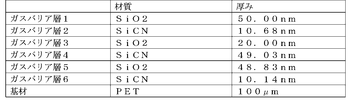
ガスバリア層を調整したガスバリア部5を用いることにより、所定の色に対する基材6単体の光透過率よりも基材6とガスバリア部5を組み合わせた光透過率を高くすることを実現している。
光変換膜4の入射側に、所定の色の光に対して、基材6単体の光透過率よりも、基材6とガスバリア部5の両方を組み合わせた物の光透過率の方が高い特徴を持つガスバリア部5を使用することにより、同じ光量の入射光1でも、ガスバリア部5を使用しないで基材6単体を使用する場合に比べ、光変換膜4に到達する光変換される光量が上がることより、光変換膜4で変換後の光量も上がり、高い出力輝度が得られる。また、従来と同じ出力輝度の場合には、消費電力が少なくなる。
本発明の実施例2を図1(B)を参照しながら説明する。図1(B)は、本発明の実施例2における光変換部材の概略構成を説明する図である。
光変換部材3は、図1(B)に示すように、入射光1の所定の色の光を光変換し、出力光2として出力する光変換膜4と、入射光1側に光変換膜4への水分やガスの浸入を防ぐ一層以上のガスバリア層からなるガスバリア部5と、ガスバリア部5の入射光1側に光変換膜4とのガスバリア部5を保持する基材6を備えている。
また、光変換膜4の出力光2側には、光変換膜4への水分、ガスの浸入を防ぐ一層以上のガスバリア層からなるガスバリア部7と、光変換膜4の出力側に光変換膜4とのガスバリア部7を保持する基材8を備えている。
また、光変換膜4の出力光2側には、光変換膜4への水分、ガスの浸入を防ぐ一層以上のガスバリア層からなるガスバリア部7と、光変換膜4の出力側に光変換膜4とのガスバリア部7を保持する基材8を備えている。
光変換膜4は、実施例1と同様、量子ドットや蛍光体などを含み、例えば、青色の光を赤色、緑色、青色の光に変換するものである。ただし、水分やガスの浸入により、光変換率が低下するため、ガスバリア部5およびガアスバリア部7によりバリアされている。
ガスバリア部5、ガスバリア部7を構成するガスバリア層は、実施例1と同様、例えば、SiCN、SiO2などの光を通す無機物からなる。ガスバリア層が多層の場合、積層面の平滑性の改善やガスバリア層間の密着力を上げる性質をもつ層(中間層)が設けられている場合があるが、本実施例では中間層も含めてガスバリア層と定義する。
各ガスバリア層の材質は異なっていてもよいし、同じでもよい。また各ガスバリア層の厚みは異なっていてもよいし、同じでもよい。
また、ガスバリア部5を構成するガスバリア層は一層以上でよく、積層数にはこだわらない。入射光1側のガスバリア部5に、図3に示すような所定の色の光透過率を他の色の光透過率より大きく山をもった分布になるように大きく際立たせる特徴を持たせる場合には、2層以上のバリア層でガスバリア部5を構成することが好ましい。
基材6、基材8は、透明性が高いフィルムが望ましい。例えば、PENやPET等のフィルムでもよいし、異なっていてもよい。また、基材6と基材8は、材質または厚みが同じでもよいし、異なっていてもよい。
本発明に用いるガスバリア部5は、所定の色の光(波長)に対して、基材6とガスバリア部5の両方を組み合わせた物の光透過率が、基材6単体の光透過率よりも高くなるように、ガスバリア部5を形成するガスバリア層の光屈折率を選定し、ガスバリア層の厚みを調整している。
本発明に用いるガスバリア部7は、少なくとも赤色、緑色、青色の光(波長)に対して、基材8とガスバリア部7の両方を組み合わせた物の光透過率が、基材8単体の光透過率よりも高くなるように、ガスバリア部7を形成するガスバリア層の光屈折率を選定し、ガスバリア層の厚みを調整している。
一例として可視光に対し、基材8を図3に示す事例と同じ材質及び同じ厚みとし、基材8とガスバリア部7を組み合わせた物の光透過率が上がるようにガスバリア部7を構成するガスバリア層を調整したガスバリア部7を用いた例を図4に示す。
ここで図4において、破線は、基材単体とガスバリア層を組み合わせた物の光透過率が、可視光の範囲で基材単体の光透過率より高くなるようガスバリア層を形成した基材であり、実線は、ガスバリア層を形成する前の基材単体である。
図4に用いた基材及びガスバリア部を構成するガスバリア層の構成を表3に示す。
表3において、ガスバリア層1からガスバリア層6の数字の順序の配置にて形成されており、基材に近い方がガスバリア層6である。
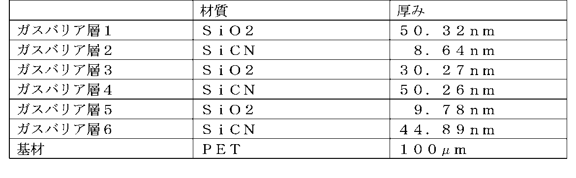
ガスバリア層を調整したガスバリア部7を用いることにより、可視光に対する基材8単体の光透過率よりも基材8とガスバリア部7を組み合わせた光透過率を高くすることを実現している。
この光変換部材3を使用することにより、この光変換部材3を使用しないで基材6単体を使用する場合に比べ、同じ光量の入射光1でも、光変換膜4に到達する所定の光の光量が、上がることより、光変換膜4で変換後の光量も上がる。また、出力側の光透過率も上がることから、出力光2の光量も更に上がり、更に高い出力輝度が得られる。また、従来と同じ出力輝度の場合には、消費電力が更に少なくなる。
実施例2において、入射光1に青色LED等から照射される青色の光の波長の範囲を際立たせた青色光を用い、光変換膜4として、量子ドットを含む光変換膜を用いた場合、特に赤色、緑色、青色の光に対し、出力側のガスバリア部7は、基材8単体の光透過率よりも基材8とガスバリア部7の両方を組み合わせた物の光透過率が高いことを特徴とするガスバリア部7を使用するとより効果的である。
特に量子ドットを含む光変換膜は、青色LED等から照射される青色の光をそれぞれ各色の光の波長の範囲を際立たせた赤色、緑色の光に光変換するため、ガスバリア部7と基材8の両方を組み合わせた光透過率が、それらの光にピークが立った特性を有していることが望ましい。これにより、更に輝度の高い赤色、緑色、青色の光をこの光変換膜4で出力することができる。
また、実施例2の構成において、入射光1に青色LED等から照射される青色光を用い、光変換膜4として、青色を白色光に変換する黄色蛍光体を含む光透過膜を用いた場合、出力側のガスバリア部7は、基材8単体の光透過率よりも基材8とガスバリア部7の両方を組み合わせた物の光透過率が、図4のように可視光全域に対しバランスよく高いことを特徴とするガスバリア部7を使用するとより効果的である。
本発明の光変換部材をディスプレイに用いてもよい。
本発明の光変換部材をディスプレイに使用することで、高い出力輝度が得られ、色域を拡大できる。また、従来と同じ出力輝度の場合には、消費電力が小さくできる。
以上の光変換部材により、バリア層を形成しても、高い出力輝度を得ることができる。
ここで、本発明の光変換部材は、以上で説明した形態に限らず、本発明の範囲内において他の形態であってもよい。たとえば、本発明の所定の色は、例えば紫外等の可視光範囲以外も含んでもよい。
1 入射光
2 出力光
3 光変換部材
4 光変換膜
5 ガスバリア部
6 基材
7 ガスバリア部
8 基材光変換部材
2 出力光
3 光変換部材
4 光変換膜
5 ガスバリア部
6 基材
7 ガスバリア部
8 基材光変換部材
Claims (4)
- 光の色を所定の色から変換する光変換膜と、
前記光変換膜の変換する光が入射する面側に位置し、前記光変換膜への水分、ガスの浸入を防ぐ一層以上のガスバリア層からなる第1のガスバリア部と、
前記第1のガスバリア部の前記光変換膜が位置する面と反対面側に位置し、光を透過し、前記光変換膜および前記第1のガスバリア部を保持する第1の基材と、
を有し、
前記所定の色の光に対して、前記第1の基材の光透過率よりも、前記第1の基材と前記第1のガスバリア部の両方を組み合わせた物の光透過率の方が高い特徴を持つ前記第1のガスバリア部を使用した光変換部材。 - 前記光変換膜の変換された光が出力される面側に位置し、前記光変換膜への水分、ガスの浸入を防ぐ一層以上のガスバリア層からなる第2のガスバリア部と、
前記第2のガスバリア部の前記光変換膜が位置する面と反対面側に位置し、光を透過し、前記光変換膜および前記第2のガスバリア部を保持する第2の基材と、
を有し、
少なくとも赤色、緑色、青色の光に対して、前記第2の基材の光透過率よりも、前記第2の基材と前記第2のガスバリア部の両方を組み合わせた物の光透過率の方が高い特徴を持つ前記第2のガスバリア部を使用した、請求項1に記載の光変換部材。 - 前記光変換膜は量子ドットもしくは蛍光体を含んだ樹脂を使用し、
前記所定の色の光は青色である請求項1または2に記載の光変換部材。 - 請求項1から3のいずれかの光変換部材を有するディスプレイ。
Priority Applications (2)
| Application Number | Priority Date | Filing Date | Title |
|---|---|---|---|
| US16/464,864 US11409164B2 (en) | 2016-12-05 | 2017-10-31 | Light conversion member |
| CN201780073087.7A CN109983373B (zh) | 2016-12-05 | 2017-10-31 | 光转换部件 |
Applications Claiming Priority (2)
| Application Number | Priority Date | Filing Date | Title |
|---|---|---|---|
| JP2016-235709 | 2016-12-05 | ||
| JP2016235709A JP6800721B2 (ja) | 2016-12-05 | 2016-12-05 | 光変換部材 |
Publications (1)
| Publication Number | Publication Date |
|---|---|
| WO2018105272A1 true WO2018105272A1 (ja) | 2018-06-14 |
Family
ID=62490910
Family Applications (1)
| Application Number | Title | Priority Date | Filing Date |
|---|---|---|---|
| PCT/JP2017/039361 Ceased WO2018105272A1 (ja) | 2016-12-05 | 2017-10-31 | 光変換部材 |
Country Status (4)
| Country | Link |
|---|---|
| US (1) | US11409164B2 (ja) |
| JP (1) | JP6800721B2 (ja) |
| CN (1) | CN109983373B (ja) |
| WO (1) | WO2018105272A1 (ja) |
Cited By (1)
| Publication number | Priority date | Publication date | Assignee | Title |
|---|---|---|---|---|
| EP3680942A1 (en) * | 2019-01-13 | 2020-07-15 | InnoLux Corporation | Lighting device |
Families Citing this family (1)
| Publication number | Priority date | Publication date | Assignee | Title |
|---|---|---|---|---|
| JP6800721B2 (ja) * | 2016-12-05 | 2020-12-16 | 東レエンジニアリング株式会社 | 光変換部材 |
Citations (4)
| Publication number | Priority date | Publication date | Assignee | Title |
|---|---|---|---|---|
| WO2004101276A1 (ja) * | 2003-05-16 | 2004-11-25 | Toppan Printing Co., Ltd. | 透明ガスバリア積層フィルム、これを用いたエレクトロルミネッセンス発光素子、エレクトロルミネッセンス表示装置、及び電気泳動式表示パネル |
| WO2015147096A1 (ja) * | 2014-03-26 | 2015-10-01 | リンテック株式会社 | シート状封止材、封止シートおよび電子デバイス封止体 |
| JP2016122211A (ja) * | 2014-07-18 | 2016-07-07 | 凸版印刷株式会社 | 波長変換シート用保護フィルム、波長変換シート及びバックライトユニット |
| JP2017094557A (ja) * | 2015-11-20 | 2017-06-01 | 凸版印刷株式会社 | ガスバリア性積層フィルム及び波長変換シート |
Family Cites Families (5)
| Publication number | Priority date | Publication date | Assignee | Title |
|---|---|---|---|---|
| JP6087872B2 (ja) * | 2013-08-12 | 2017-03-01 | 富士フイルム株式会社 | 光学フィルム、バリアフィルム、光変換部材、バックライトユニットおよび液晶表示装置 |
| JP6230974B2 (ja) | 2013-08-26 | 2017-11-15 | 富士フイルム株式会社 | 光変換部材、バックライトユニット、および液晶表示装置、ならびに光変換部材の製造方法 |
| JP6117758B2 (ja) * | 2014-09-30 | 2017-04-19 | 富士フイルム株式会社 | 積層フィルム、バックライトユニット、液晶表示装置、および、積層フィルムの製造方法 |
| WO2016075950A1 (ja) * | 2014-11-14 | 2016-05-19 | 富士フイルム株式会社 | 波長変換部材及びそれを備えたバックライトユニット、液晶表示装置 |
| JP6800721B2 (ja) * | 2016-12-05 | 2020-12-16 | 東レエンジニアリング株式会社 | 光変換部材 |
-
2016
- 2016-12-05 JP JP2016235709A patent/JP6800721B2/ja active Active
-
2017
- 2017-10-31 WO PCT/JP2017/039361 patent/WO2018105272A1/ja not_active Ceased
- 2017-10-31 US US16/464,864 patent/US11409164B2/en active Active
- 2017-10-31 CN CN201780073087.7A patent/CN109983373B/zh active Active
Patent Citations (4)
| Publication number | Priority date | Publication date | Assignee | Title |
|---|---|---|---|---|
| WO2004101276A1 (ja) * | 2003-05-16 | 2004-11-25 | Toppan Printing Co., Ltd. | 透明ガスバリア積層フィルム、これを用いたエレクトロルミネッセンス発光素子、エレクトロルミネッセンス表示装置、及び電気泳動式表示パネル |
| WO2015147096A1 (ja) * | 2014-03-26 | 2015-10-01 | リンテック株式会社 | シート状封止材、封止シートおよび電子デバイス封止体 |
| JP2016122211A (ja) * | 2014-07-18 | 2016-07-07 | 凸版印刷株式会社 | 波長変換シート用保護フィルム、波長変換シート及びバックライトユニット |
| JP2017094557A (ja) * | 2015-11-20 | 2017-06-01 | 凸版印刷株式会社 | ガスバリア性積層フィルム及び波長変換シート |
Cited By (3)
| Publication number | Priority date | Publication date | Assignee | Title |
|---|---|---|---|---|
| EP3680942A1 (en) * | 2019-01-13 | 2020-07-15 | InnoLux Corporation | Lighting device |
| CN111435671A (zh) * | 2019-01-13 | 2020-07-21 | 群创光电股份有限公司 | 发光装置 |
| CN111435671B (zh) * | 2019-01-13 | 2024-01-09 | 群创光电股份有限公司 | 发光装置 |
Also Published As
| Publication number | Publication date |
|---|---|
| US20190302536A1 (en) | 2019-10-03 |
| CN109983373A (zh) | 2019-07-05 |
| US11409164B2 (en) | 2022-08-09 |
| CN109983373B (zh) | 2021-10-22 |
| JP6800721B2 (ja) | 2020-12-16 |
| JP2018092017A (ja) | 2018-06-14 |
Similar Documents
| Publication | Publication Date | Title |
|---|---|---|
| JP6163754B2 (ja) | 発光装置に用いるバンドパスフィルタおよびこれを用いた発光装置 | |
| CN103715217B (zh) | 增亮型自发光型显示器 | |
| CN109709710A (zh) | 颜色转换元件和包括该颜色转换元件的显示设备 | |
| WO2012035760A1 (ja) | バックライト装置、およびそのバックライト装置を用いた液晶表示装置、およびそれらに用いる発光ダイオード | |
| KR102113858B1 (ko) | 발광 다이오드용 광대역 유전 반사기 | |
| CN106133562A (zh) | 波长转换片、背光单元以及荧光体用保护薄膜 | |
| WO2016169068A1 (zh) | 液晶显示面板和液晶显示器 | |
| JP2010287524A (ja) | 表示素子および表示装置 | |
| US10243115B2 (en) | Semiconductor component | |
| JP2017181901A (ja) | 発光部材、およびこれを含む表示装置 | |
| WO2019072041A1 (zh) | 显示面板、显示装置和显示面板的制作方法 | |
| TW201403901A (zh) | 有機發光二極體、包含其之顯示面板及顯示裝置 | |
| US20190187355A1 (en) | Display device | |
| TW201814376A (zh) | 光源模組 | |
| EP3578879B1 (en) | Optical member and display including the same | |
| JP2016095947A (ja) | 発光装置、バックライト装置及び表示装置 | |
| WO2018105272A1 (ja) | 光変換部材 | |
| Oh et al. | Improved color coordinates of green monochromatic pc-LED capped with a band-pass filter | |
| KR101736880B1 (ko) | 양자점층 및 광학필터를 포함하는 디스플레이 장치 | |
| TWI691765B (zh) | 顯示裝置 | |
| TWI788867B (zh) | 光源模組及顯示裝置 | |
| JP2017136737A (ja) | 蛍光体用保護フィルム、及びそれを用いた波長変換シート | |
| TWM634983U (zh) | 微發光二極體顯示裝置 | |
| JP2020042137A (ja) | 光学フィルム、光学バリアフィルム、及び波長変換フィルム | |
| JP2023541280A5 (ja) |
Legal Events
| Date | Code | Title | Description |
|---|---|---|---|
| 121 | Ep: the epo has been informed by wipo that ep was designated in this application |
Ref document number: 17878008 Country of ref document: EP Kind code of ref document: A1 |
|
| NENP | Non-entry into the national phase |
Ref country code: DE |
|
| 122 | Ep: pct application non-entry in european phase |
Ref document number: 17878008 Country of ref document: EP Kind code of ref document: A1 |