WO2018092855A1 - 駆動回路およびインピーダンス整合装置 - Google Patents
駆動回路およびインピーダンス整合装置 Download PDFInfo
- Publication number
- WO2018092855A1 WO2018092855A1 PCT/JP2017/041328 JP2017041328W WO2018092855A1 WO 2018092855 A1 WO2018092855 A1 WO 2018092855A1 JP 2017041328 W JP2017041328 W JP 2017041328W WO 2018092855 A1 WO2018092855 A1 WO 2018092855A1
- Authority
- WO
- WIPO (PCT)
- Prior art keywords
- switching element
- pin diode
- state
- limiting resistor
- current limiting
- Prior art date
- Legal status (The legal status is an assumption and is not a legal conclusion. Google has not performed a legal analysis and makes no representation as to the accuracy of the status listed.)
- Ceased
Links
Images




Classifications
-
- H—ELECTRICITY
- H03—ELECTRONIC CIRCUITRY
- H03K—PULSE TECHNIQUE
- H03K17/00—Electronic switching or gating, i.e. not by contact-making and –breaking
- H03K17/51—Electronic switching or gating, i.e. not by contact-making and –breaking characterised by the components used
- H03K17/74—Electronic switching or gating, i.e. not by contact-making and –breaking characterised by the components used by the use, as active elements, of diodes
-
- H—ELECTRICITY
- H01—ELECTRIC ELEMENTS
- H01J—ELECTRIC DISCHARGE TUBES OR DISCHARGE LAMPS
- H01J37/00—Discharge tubes with provision for introducing objects or material to be exposed to the discharge, e.g. for the purpose of examination or processing thereof
- H01J37/32—Gas-filled discharge tubes
- H01J37/32009—Arrangements for generation of plasma specially adapted for examination or treatment of objects, e.g. plasma sources
- H01J37/32082—Radio frequency generated discharge
- H01J37/32174—Circuits specially adapted for controlling the RF discharge
- H01J37/32183—Matching circuits
-
- H—ELECTRICITY
- H03—ELECTRONIC CIRCUITRY
- H03H—IMPEDANCE NETWORKS, e.g. RESONANT CIRCUITS; RESONATORS
- H03H11/00—Networks using active elements
- H03H11/02—Multiple-port networks
- H03H11/28—Impedance matching networks
- H03H11/30—Automatic matching of source impedance to load impedance
-
- H—ELECTRICITY
- H03—ELECTRONIC CIRCUITRY
- H03H—IMPEDANCE NETWORKS, e.g. RESONANT CIRCUITS; RESONATORS
- H03H7/00—Multiple-port networks comprising only passive electrical elements as network components
- H03H7/01—Frequency selective two-port networks
-
- H—ELECTRICITY
- H03—ELECTRONIC CIRCUITRY
- H03H—IMPEDANCE NETWORKS, e.g. RESONANT CIRCUITS; RESONATORS
- H03H7/00—Multiple-port networks comprising only passive electrical elements as network components
- H03H7/01—Frequency selective two-port networks
- H03H7/0115—Frequency selective two-port networks comprising only inductors and capacitors
-
- H—ELECTRICITY
- H03—ELECTRONIC CIRCUITRY
- H03H—IMPEDANCE NETWORKS, e.g. RESONANT CIRCUITS; RESONATORS
- H03H7/00—Multiple-port networks comprising only passive electrical elements as network components
- H03H7/38—Impedance-matching networks
- H03H7/40—Automatic matching of load impedance to source impedance
-
- H—ELECTRICITY
- H05—ELECTRIC TECHNIQUES NOT OTHERWISE PROVIDED FOR
- H05H—PLASMA TECHNIQUE; PRODUCTION OF ACCELERATED ELECTRICALLY-CHARGED PARTICLES OR OF NEUTRONS; PRODUCTION OR ACCELERATION OF NEUTRAL MOLECULAR OR ATOMIC BEAMS
- H05H1/00—Generating plasma; Handling plasma
- H05H1/24—Generating plasma
- H05H1/46—Generating plasma using applied electromagnetic fields, e.g. high frequency or microwave energy
Definitions
- the present invention relates to a drive circuit that switches an on state and an off state of a PIN diode, and an impedance matching device using the drive circuit.
- the diode has a characteristic of being in a conductive state (ON state) when a forward voltage is applied and being in an open state (OFF state) when a reverse voltage is applied.
- a diode may be used as a switch using this characteristic.
- a diode for example, a PIN diode is used.
- Patent Document 1 discloses an example of a drive circuit that switches between an on state and an off state of a conventional PIN diode.
- the drive circuit disclosed in this document includes two switching elements.
- the bias power supply + VD is supplied to the output terminal of the drive circuit, and the power supply
- the bias power supply -VS is supplied to the output terminal of the drive circuit.
- the output terminal is connected to an input terminal of a PIN diode.
- a bias power supply + VD is supplied to the input terminal, a forward voltage is applied to the PIN diode, and the PIN diode is turned on.
- the bias power source -VS is supplied to the input terminal, a reverse voltage is applied to the PIN diode, and the PIN diode is turned off.
- the PIN diode is connected to a power supply line that connects the high-frequency input unit and the high-frequency output unit, and the switching between the ON state and the OFF state of the PIN diode is performed while a high-frequency current is flowing. Has been done. Switching in such an energized state is called “hot switching”.
- hot switching in hot switching in a state where a high-frequency current is flowing, the switching time from the ON state to the OFF state of the PIN diode is long (switching speed is slow), that is, the PIN diode carrier. If the transition time is long, the power loss increases.
- the drive circuit disclosed in Patent Document 2 includes a bootstrap circuit, a clamp network, and the like, and adjusts the switching speed.
- the bootstrap circuit and the clamp network are used, the circuit configuration and control are complicated.
- an object of the present invention is to provide a drive circuit capable of suppressing a decrease in reliability of a PIN diode due to hot switching with a simple circuit configuration, and an object of the present invention is to provide an impedance matching device using a drive circuit.
- the drive circuit provided by the first aspect of the present invention is a drive circuit that switches between an on state and an off state of a PIN diode, and when one is on, the other is off.
- a forward voltage is applied to the PIN diode from the drive power supply via the current limiting resistor, thereby turning on the PIN diode, and the first switching element.
- the current limiting resistor is supplied from the drive power supply. Not through, by applying a reverse voltage to the PIN diode, characterized in that the PIN diode in the OFF state.
- a reverse voltage is applied to the PIN diode without passing through the current limiting resistor, so that the PIN diode is turned off in a short transition time. Can be switched.
- the calorific value of the PIN diode can be suppressed. Therefore, it is possible to suppress a decrease in reliability of the PIN diode due to hot switching.
- the on-resistance of the second switching element is 0.1 ⁇ or less. According to this configuration, since the resistance value in the current path when the PIN diode is changed from the on state to the off state is reduced, the transition time from the on state to the off state of the PIN diode can be further shortened.
- a forward current of the PIN diode generated by the forward voltage is determined by an on-resistance of the first switching element and the current limiting resistor, and a resistance of the current limiting resistor. The value is determined based on the on-resistance of the first switching element so that the forward current of the PIN diode becomes a predetermined current value.
- a predetermined current value for example, 1 A or more
- the PIN diode is switched from the off state to the on state with a transition time sufficiently shorter than the carrier life of the PIN diode. be able to.
- the first switching element, the current limiting resistor, and the second switching element are:
- the PIN diodes are connected in series, and the anode terminal of the PIN diode is connected to a connection point between the current limiting resistor and the second switching element, and the cathode terminal is grounded.
- the forward voltage is applied to the PIN diode through the current limiting resistor
- a reverse voltage can be applied to the PIN diode without going through the current limiting resistor. Therefore, the current limiting resistor can be prevented from passing through the current path when the PIN diode is turned from the on state to the off state.
- the current limiting resistor, the first switching element, and the second switching element are sequentially arranged from a positive output terminal to a negative output terminal of the drive power supply.
- the PIN diode has an anode terminal connected to a connection point between the first switching element and the second switching element, and a cathode terminal grounded.
- the second switching element, the current limiting resistor, and the first switching element in order from the positive output terminal to the negative output terminal of the drive power supply. are connected in series, and the PIN diode has an anode terminal grounded and a cathode terminal connected to a connection point between the current limiting resistor and the second switching element. Even with this configuration, it is possible to prevent the current limiting resistor from being interposed in the current path when the PIN diode is switched from the on state to the off state.
- the second switching element, the first switching element, and the current limiting resistor are sequentially arranged from the positive output terminal to the negative output terminal of the drive power supply.
- the PIN diode has an anode terminal grounded and a cathode terminal connected to a connection point between the first switching element and the second switching element.
- a filter circuit is further provided between the connection point and the PIN diode. According to this configuration, since the high-frequency power is suppressed from being input to the first switching element and the second switching element by the filter circuit, these damages can be suppressed.
- the driving circuit further includes a speed-up capacitor connected in parallel to the current limiting resistor.
- the impedance matching device provided by the second aspect of the present invention is an impedance matching device arranged between a high-frequency power source and a load connected by a power supply line and for matching impedances, and connected in parallel to each other.
- a plurality of impedance adjustment capacitors each having one end connected to the power supply line, a plurality of PIN diodes connected in series one by one for each of the plurality of impedance adjustment capacitors,
- It includes a control circuit for inputting a driving signal for instructing the switching between the on and off states of the grayed element and the second switching element.
- the PIN diode when the PIN diode is switched from the on state to the off state, a reverse voltage is applied to the PIN diode without passing through the current limiting resistor.
- the PIN diode can be switched from the on state to the off state in a short transition time. Therefore, it is possible to suppress a decrease in reliability of the PIN diode due to hot switching.
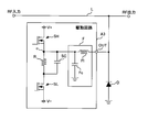
- FIG. 1 shows a circuit configuration of a drive circuit A1 for the PIN diode D according to the first embodiment.
- the drive circuit A1 inputs a drive power supply (not shown) and applies a forward bias or a reverse bias to the PIN diode D via the output terminal OUT.
- the anode terminal of the PIN diode D is connected to the output terminal OUT of the drive circuit A1, and is connected to a power supply line L through which a high-frequency current flows.
- the cathode terminal of the PIN diode D is grounded.
- the drive power source is a DC voltage source, and has a positive output terminal V + and a negative output terminal V ⁇ .
- the positive output terminal V + causes a forward voltage drop (forward current to flow to the anode terminal of the PIN diode D when a switching element SH described later is turned on and a switching element SL described later is turned off.
- the voltage necessary for the switching is applied to turn on the PIN diode D.
- the negative output terminal V ⁇ has a negative voltage (a voltage within a range not reaching the breakdown voltage) at the anode terminal of the PIN diode D when the switching element SL is turned on and the switching element SH is turned off. ) Is applied to turn off the PIN diode D.
- the drive circuit A1 applies a forward voltage to the PIN diode D via the output terminal OUT, thereby turning the PIN diode D into a conductive state (ON state) and applying a reverse voltage to the PIN diode D.
- the PIN diode D is opened (off state).
- the drive circuit A1 includes two switching elements SH and SL, a current limiting resistor R, a speed-up capacitor SC, and a filter circuit F.
- the switching elements SH and SL are circuit elements made of a semiconductor material, and are, for example, MOSFETs (Metal / Oxide / Semiconductor / Field / Effect / Transistors), bipolar transistors, IGBTs (Insulated / Gate / Bipolar / Transistors): optocouplers, and the like. .
- MOSFETs Metal / Oxide / Semiconductor / Field / Effect / Transistors
- IGBTs Insulated / Gate / Bipolar / Transistors
- Switching elements SH and SL receive a drive signal from a control circuit (not shown) at their gate terminals, and switch between an on state and an off state according to the drive signal.
- the switching elements SH and SL are controlled by the drive signal so that when one is on, the other is off.
- the control circuit generates two voltage signals in which the high level and the low level are inverted from each other, inputs one voltage signal to the switching element SH as the drive signal S1, and sets the other voltage signal as the drive signal / S1. Input to the switching element SL.
- the switching element SH (SL) When the drive signal S1 (/ S1) is a high level voltage signal, the switching element SH (SL) is turned on, and when the drive signal S1 (/ S1) is a low level voltage signal, the switching element SH (SL ) Is turned off. As a result, the switching element SH and the switching element SL are opposite to each other in the on state and the off state.
- the switching element SH corresponds to a “first switching element” recited in the claims
- the switching element SL corresponds to a “second switching element” recited in the claims.
- the switching elements SH and SL are connected in series via the current limiting resistor R.
- the switching element SH is connected to the positive side of the drive power supply, and the switching element SL is connected to the negative side of the drive power supply. Therefore, in the drive circuit A1, the switching element SH (first switching element), the current limiting resistor R, and the switching element SL (the first switching element SL) are moved from the positive output terminal V + to the negative output terminal V ⁇ of the drive power supply. These are connected in series in the order of 2 switching elements).
- the drain terminal of the switching element SH is connected to the output terminal V + on the positive side of the drive power supply, and the source terminal of the switching element SH is connected to one end of the current limiting resistor R.
- the drain terminal of the switching element SL is connected to the other end of the current limiting resistor R, and the source terminal of the switching element SL is connected to the output terminal V ⁇ on the negative side of the drive power supply.
- the gate terminals of the switching elements SH and SL are connected to the control circuit.
- a speed-up capacitor SC is connected to the current limiting resistor R in parallel.
- a connection point a between the current limiting resistor R and the switching element SL is connected to the output terminal OUT through the filter circuit F.
- the filter circuit F includes, for example, a capacitor Fc and an inductor Fl connected in an L shape. Specifically, one end of the inductor Fl and one end of the capacitor Fc are connected to the connection point a. The other end of the inductor Fl is connected to the output terminal OUT, and the other end of the capacitor Fc is grounded.
- the configuration of the filter circuit F is not limited to this. Although the filter circuit F may not be provided, when the filter circuit F is provided, the high frequency power flowing through the RF input terminal and the RF output terminal is suppressed from being input to the drive circuit A1, and the switching elements SH, SL damage can be suppressed.
- the switching element SH When the PIN diode D is in an off state, that is, when the switching element SH is in an off state and the switching element SL is in an on state, the switching element SH is turned on and the switching element SL is turned off.
- the current path from the output terminal V + on the positive side of the drive power supply to the anode terminal of the PIN diode D is conducted through the switching element SH, the current limiting resistor R or the speed-up capacitor SC, and the filter circuit F. As a result, a forward voltage is applied to the PIN diode D, and the PIN diode D is turned on.
- the transition time when the PIN diode D switches from the on state to the off state is determined by the on resistance of the switching element SL, it can be made shorter than when the current limiting resistor R is present.
- the switching element SL having a small on-resistance for example, 0.1 ⁇ or less
- the transition time can be shortened.
- the PIN diode D can be switched from the on state to the off state in a short transition time with a simple circuit configuration. Therefore, loss such as heat generation of the PIN diode D can be suppressed, and a decrease in reliability of the PIN diode D due to hot switching can be suppressed.
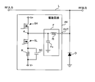
- FIG. 2 shows a drive circuit A2 for the PIN diode D according to the second embodiment. Note that the same or similar components as those of the drive circuit A1 are denoted by the same reference numerals and description thereof is omitted. As shown in the figure, the drive circuit A2 of the second embodiment differs from the drive circuit A1 of the first embodiment in the connection position of the current limiting resistor R.
- the current limiting resistor R is connected between the switching element SH and the output terminal V + on the positive side of the drive power supply, and the switching element SH and the switching element SL are directly connected. Therefore, in the drive circuit A2, the current limiting resistor R, the switching element SH, and the switching element SL are connected in series in this order from the positive output terminal V + to the negative output terminal V ⁇ of the drive power supply. ing. Specifically, the output terminal V + on the positive electrode side of the drive power supply is connected to one end of the current limiting resistor R, and the other end of the current limiting resistor R is connected to the drain terminal of the switching element SH.
- the source terminal of the switching element SH and the drain terminal of the switching element SL are connected, and the source terminal of the switching element SL and the output terminal V ⁇ on the negative side of the drive power supply are connected.
- a connection point b between the switching element SH and the switching element SL is connected to the output terminal OUT via the filter circuit F.
- the switching element SH corresponds to the “first switching element” recited in the claims
- the switching element SL corresponds to the “second switching element” recited in the claims.
- the operation is the same as that of the drive circuit A1 according to the first embodiment, so that the same effect can be obtained.
- FIG. 3 shows a drive circuit A3 for the PIN diode D according to the third embodiment.
- the third embodiment differs from the first embodiment and the second embodiment in that the connection direction of the anode terminal and the cathode terminal of the PIN diode D is opposite. Specifically, the anode terminal of the PIN diode D is grounded, and the cathode terminal of the PIN diode D is connected to the power supply line L that connects the RF input terminal and the RF output terminal.
- the output terminal OUT of the drive circuit A3 is connected to the cathode terminal of the PIN diode D.
- the drive circuit A3 is different in circuit configuration from the drive circuit A1. Specifically, in the drive circuit A1, the connection point a between the switching element SL and the current limiting resistor R is connected to the output terminal OUT via the filter circuit F. A connection point c between the element SH and the current limiting resistor R is connected to the output terminal OUT via the filter circuit F.
- the switching element SH corresponds to a “second switching element” recited in the claims
- the switching element SL corresponds to a “first switching element” recited in the claims.
- the switching element SH (second switching element), the current limiting resistor R, and the switching element SL (first output element) from the positive output terminal V + to the negative output terminal V ⁇ of the drive power supply. These are connected in series in the order of 1 switching element).
- the switching element SH When the PIN diode D is in an off state, that is, when the switching element SH is in an on state and the switching element SL is in an off state, the switching element SH is turned off and the switching element SL is turned on.
- the current path from the output terminal V ⁇ on the negative side of the drive power supply to the cathode terminal of the PIN diode D is conducted through the switching element SL, the current limiting resistor R or the speed-up capacitor SC, and the filter circuit F. As a result, a forward voltage is applied to the PIN diode D, and the PIN diode D is turned on.
- the transition time when the PIN diode D switches from the on state to the off state is determined by the on resistance of the switching element SH, it can be made shorter than when the current limiting resistor R is present.
- the switching element SH having a small on-resistance for example, 0.1 ⁇ or less
- the transition time can be shortened.
- the PIN diode D can be switched from the on state to the off state in a short transition time with a simple circuit configuration. Therefore, loss such as heat generation of the PIN diode D can be suppressed, and a decrease in reliability of the PIN diode D due to hot switching can be suppressed.
- FIG. 4 shows a drive circuit A4 for the PIN diode D according to the fourth embodiment. Note that the same or similar components as those of the drive circuits A1 to A3 are denoted by the same reference numerals and description thereof is omitted. As shown in the figure, the drive circuit A4 of the fourth embodiment differs from the drive circuit A3 of the third embodiment in the connection position of the current limiting resistor R.
- the current limiting resistor R is connected between the switching element SL and the output terminal V ⁇ on the negative side of the drive power supply, and the switching element SH and the switching element SL are directly connected. Accordingly, in the drive circuit A4, the switching element SH (second switching element) and the switching element SL (first switching element) are moved from the positive output terminal V + to the negative output terminal V ⁇ of the drive power supply. These are connected in series in the order of the current limiting resistor R. Specifically, the output terminal V + on the positive electrode side of the drive power supply and the drain terminal of the switching element SH are connected, and the source terminal of the switching element SH and the drain terminal of the switching element SL are connected.
- the source terminal of the switching element SL and one end of the current limiting resistor R are connected, and the other end of the current limiting resistor R and the output terminal V ⁇ on the negative side of the drive power supply are connected.
- a connection point d between the source terminal of the switching element SH and the drain terminal of the switching element SL is connected to the output terminal OUT via the filter circuit F.
- the switching element SH corresponds to a “second switching element” recited in the claims
- the switching element SL corresponds to a “first switching element” recited in the claims.
- the operation is the same as that of the drive circuit A3 according to the third embodiment, so that the same effect can be obtained.
- the PIN diode D drive circuits A1 to A4 described above are used in, for example, an impedance matching device in a high-frequency power supply system.
- the high-frequency power supply system will be described below as a fifth embodiment of the present invention.
- FIG. 5 shows an example of the overall configuration of the high-frequency power supply system according to the fifth embodiment of the present invention.
- the high-frequency power supply system includes a high-frequency power source 1, a load 2, and an impedance matching device 3.
- the high frequency power supply 1 and the load 2 are connected by a power supply line 4, and an impedance matching device 3 is disposed between them.
- the high-frequency power supply system is a system that supplies high-frequency power generated by a high-frequency power source 1 to a load 2 via a power line 4.
- the power supply line 4 corresponds to the power supply line L in FIGS.
- the high frequency power source 1 outputs high frequency power.
- the high frequency power source 1 converts AC power from the power system into DC power using a rectifier circuit, converts DC power into high frequency power using an inverter circuit, and outputs the DC power.
- the high frequency power supply 1 includes a power supply control circuit (not shown) and controls output power and output current.
- the high frequency power source 1 outputs high frequency power of 13.56 MHz, for example.
- the configuration and frequency of the high frequency power supply 1 are not limited.
- the load 2 performs various processes using high-frequency power input from the high-frequency power source 1.
- An example of such a load 2 is a plasma processing apparatus, a plasma generation apparatus, a non-contact power transmission apparatus, or the like.
- a plasma processing apparatus is an apparatus that includes a workpiece processing unit and processes (for example, etching, CVD, etc.) a workpiece such as a semiconductor wafer or a liquid crystal substrate carried into the workpiece processing unit.
- the plasma processing apparatus introduces a plasma discharge gas into the workpiece processing portion, and applies high-frequency power (voltage) supplied from the high-frequency power source 1 to the plasma discharge gas.
- the gas is ionized to change from the non-plasma state to the plasma state.
- the plasma processing apparatus processes a workpiece using a gas in a plasma state.
- a plasma generator is an apparatus that ionizes a plasma discharge gas to change from a non-plasma state to a plasma state, and supplies the plasma state gas to a plasma chamber or the like.
- the plasma state changes from moment to moment as the manufacturing process such as plasma etching and plasma CVD progresses.
- the impedance of the load 2 varies. Therefore, in order to efficiently supply power from the high frequency power source 1 to the load 2, the high frequency power supply system has an impedance (hereinafter, referred to as the load 2) viewed from the output end of the high frequency power source 1 as the impedance of the load 2 varies.
- Impedance matching device 3 for adjusting “load side impedance”) is provided.
- the impedance matching device 3 performs impedance matching by adjusting the load side impedance.
- the impedance matching device 3 includes a drive circuit A1 and a PIN diode D according to the first embodiment.
- FIG. 6 shows an example of a detailed circuit configuration of the impedance matching device 3.
- the impedance matching device 3 includes an impedance detection unit 31, a control circuit 32, and an impedance adjustment circuit 33.
- the impedance detector 31 is arranged at the input end of the impedance matching device 3 and detects the load side impedance.
- the impedance detection unit 31 outputs the detected load side impedance to the control circuit 32. Specifically, the impedance detection unit 31 detects a current corresponding to the high-frequency current flowing in the power supply line 4 and a voltage corresponding to the high-frequency voltage generated in the power supply line 4, and the current effective value is detected from the detected current signal and voltage signal. The effective voltage value and the phase difference between the current signal and the voltage signal are obtained. Then, the load side impedance is calculated using these parameters, and this is output to the control circuit 32.
- the configuration of the impedance detection unit 31 and the load side impedance detection method are not limited to this.
- the control circuit 32 controls the impedance adjustment circuit 33 so that the load-side impedance input from the impedance detection unit 31 becomes a predetermined impedance value (for example, impedance viewed from the output terminal of the high-frequency power source 1 when viewed from the high-frequency power source 1). It is something to control.
- a predetermined impedance value for example, impedance viewed from the output terminal of the high-frequency power source 1 when viewed from the high-frequency power source 1). It is something to control.
- the impedance adjustment circuit 33 includes a capacitance variable circuit 331, a fixed capacitor 332, and an inductor 333. Note that the fixed capacitor 332 may not be provided.
- the impedance adjustment circuit 33 adjusts the load side impedance by changing the capacitance of the capacitance variable circuit 331.
- the capacitance variable circuit 331 includes a plurality of adjustment capacitors (impedance adjustment capacitors) Cd, a plurality of PIN diodes D, and a plurality of drive circuits A1, and can change the capacitance.
- one PIN diode D is connected in series to each adjustment capacitor Cd, and a series body of the adjustment capacitor Cd and the PIN diode D is connected in parallel to each other.
- One end of each adjustment capacitor Cd is connected to the power supply line 4, and the other end is connected to the anode terminal of each PIN diode D.
- the cathode terminal of each PIN diode D is grounded.
- the capacitances of the adjustment capacitors Cd are different from each other, and are set to increase in binary steps such as 1 pF, 2 pF, 4 pF,. In addition, you may make it use the thing of the same capacitance. Further, the capacitance of each adjustment capacitor Cd is not limited to a configuration in which all the capacitances are different from each other or all the capacitances are the same. For example, a plurality of adjustment capacitors Cd whose capacitance increases in binary steps, such as 1 pF, 2 pF, 4 pF,. May be combined. Further, it does not mean that a predetermined capacitance is realized with one capacitor.
- a capacitance of 10 pF may be connected in parallel, or a capacitance of 20 pF may be connected in series.
- the capacitance variable circuit 331 may include a capacitor that does not change capacitance, one end of which is connected to the power supply line 4 and the other end is grounded.
- a drive circuit A1 is connected to each PIN diode D.
- the fixed capacitor 332 and the inductor 333 are connected in series to the power supply line 4, and the capacitance variable circuit 331 is upstream of the power supply line 4 from these. Is arranged.
- the connection position between the fixed capacitor 332 and the inductor 333 is not limited to the above.
- the variable capacitance circuit 331, the fixed capacitor 332, and the inductor 333 may be connected to an L type, a ⁇ type, a T type, or the like.
- the load side impedance detected by the impedance detection unit 31 is output to the control circuit 32.
- the control circuit 32 generates the drive signals S1 and / S1 to be input to each drive circuit A1 so that the input load side impedance becomes a predetermined impedance.
- the generated drive signals S1, / S1 are respectively input to the switching elements SH, SL of each drive circuit A1.
- the ON state and the OFF state of the PIN diode D to which the drive circuit A1 is connected are switched by the operation shown in the first embodiment.
- the impedance matching device 3 adjusts the capacitance of the capacitance variable circuit 331 by controlling the on state and the off state of each PIN diode D to adjust the load side impedance.
- the ON state and the OFF state of the PIN diode D are switched by the drive circuit A1.
- a decrease in the reliability of the PIN diode D due to hot switching can be suppressed, so that the switching of the PIN diode D between the on state and the off state can be performed appropriately. Therefore, impedance matching by the impedance matching device 3 can be performed appropriately.
- the impedance matching device 3 can adjust the load side impedance at high speed. Therefore, in the high frequency power supply system, high frequency power can be efficiently supplied from the high frequency power source 1 to the load 2.
- the impedance matching device 3 detects the load side impedance by the impedance detection unit 31, and the control circuit 32 controls the impedance adjustment circuit 33 based on the load side impedance.
- the control circuit 32 controls the impedance adjustment circuit 33 so that the reflected wave power becomes low. You may make it do.
- the case where the impedance matching device 3 includes the drive circuit A1 according to the first embodiment has been described as an example.
- the drive circuits A2 to A4 according to the fourth embodiment may be provided. Further, it may be a combination of drive circuits A1 to A4.
- the PIN diode driving circuit and the impedance matching device using the driving circuit according to the present invention are not limited to the above-described embodiments.
- the specific configuration of each part of the drive circuit and the impedance matching device of the present invention can be varied in design in various ways.
- A1, A2, A3, A4 Drive circuit D Diode SH, SL Switching element R Current limiting resistor SC Speed-up capacitor F Filter circuit Fc Capacitor Fl Inductor 1 High frequency power supply 2 Load 3 Impedance matching device 31 Impedance detection unit 32 Control circuit 33 Impedance adjustment Circuit 331 Capacitance variable circuit Cd Adjustment capacitor 332 Fixed capacitor 333 Inductor
Landscapes
- Physics & Mathematics (AREA)
- Engineering & Computer Science (AREA)
- Plasma & Fusion (AREA)
- Electromagnetism (AREA)
- Spectroscopy & Molecular Physics (AREA)
- Chemical & Material Sciences (AREA)
- Analytical Chemistry (AREA)
- Power Engineering (AREA)
- Power Conversion In General (AREA)
- Electronic Switches (AREA)
- Plasma Technology (AREA)
- Filters And Equalizers (AREA)
- Networks Using Active Elements (AREA)
Abstract
PINダイオード(D)のオン状態とオフ状態とを切り替える駆動回路(A1)であって、スイッチング素子(SH)およびスイッチング素子(SL)と、駆動電源と、PINダイオード(D)の順方向電流を調整する電流制限抵抗(R)とを備えている。そして、スイッチング素子(SH)がオン状態であり、かつ、スイッチング素子(SL)がオフ状態のとき、前記駆動電源から、電流制限抵抗(R)を介して、PINダイオード(D)に順方向電圧を印加することで、PINダイオード(D)をオン状態にし、スイッチング素子(SH)がオフ状態であり、かつ、スイッチング素子(SL)がオン状態のとき、前記駆動電源から、電流制限抵抗(R)を介さず、PINダイオード(D)に逆方向電圧を印加することで、PINダイオード(D)をオフ状態にする。
Description
本発明は、PINダイオードのオン状態とオフ状態とを切り替える駆動回路、および、当該駆動回路を用いたインピーダンス整合装置に関する。
ダイオードは、順方向電圧を印加すると導通状態(オン状態)になり、逆方向電圧を印加すると開放状態(オフ状態)になる特性を有している。この特性を用いて、ダイオードをスイッチとして利用されることがある。このようなダイオードとしては、例えば、PINダイオードが用いられる。特許文献1は、従来のPINダイオードのオン状態とオフ状態とを切り替える駆動回路の一例を開示している。同文献に開示された駆動回路は、2つのスイッチング素子を備えており、電源の正極側に配置されたスイッチング素子がオン状態のとき、駆動回路の出力端にバイアス電源+VDを供給し、電源の負極側に配置されたスイッチング素子がオン状態のとき、駆動回路の出力端にバイアス電源-VSを供給する。前記出力端は、PINダイオードの入力端に接続されており、前記入力端にバイアス電源+VDが供給されると、PINダイオードに順方向電圧が印加され、PINダイオードがオン状態となる。一方、前記入力端にバイアス電源-VSが供給されると、PINダイオードに逆方向電圧が印加され、PINダイオードがオフ状態となる。
上記特許文献1において、PINダイオードは、高周波入力部と高周波出力部とを繋ぐ電源ライン上に接続されており、PINダイオードのオン状態とオフ状態との切り替えは、高周波電流が流れている状態で行われている。このような通電状態でのスイッチングは「ホットスイッチング」と呼ばれている。特に、上記特許文献1のように、高周波電流が流れている状態でのホットスイッチングにおいて、PINダイオードのオン状態からオフ状態への切り替え時間が長い(スイッチングスピードが遅い)、すなわち、PINダイオードのキャリアの遷移時間が長いと、電力損失が大きくなる。この電力損失により、例えば、PINダイオードの発熱量が大きくなり、PINダイオードの信頼性が低下するという問題があった。そのため、PINダイオードをオン状態からオフ状態に切り替える時には、より短い遷移時間で行う必要があった。
このような問題を解決するために、特許文献2に開示された駆動回路は、ブートストラップ回路やクランプネットワークなどを備え、スイッチングスピードを調整している。しかし、ブートストラップ回路やクランプネットワークなどを用いているため、回路構成や制御が複雑になってしまっていた。
そこで、本発明は、上記課題に鑑みて創作されたものであり、その目的は、簡易な回路構成により、ホットスイッチングによるPINダイオードの信頼性の低下を抑制することができる駆動回路、および、当該駆動回路を用いたインピーダンス整合装置を提供することにある。
本発明の第1の側面によって提供される駆動回路は、PINダイオードのオン状態とオフ状態とを切り替える駆動回路であって、一方がオン状態のときに他方がオフ状態となる、第1のスイッチング素子および第2のスイッチング素子と、直流電圧を発生させる駆動電源と、前記PINダイオードの順方向電流を調整する電流制限抵抗と、を備え、前記第1のスイッチング素子がオン状態であり、かつ、前記第2のスイッチング素子がオフ状態のとき、前記駆動電源から、前記電流制限抵抗を介して、前記PINダイオードに順方向電圧を印加することで、前記PINダイオードをオン状態にし、前記第1のスイッチング素子がオフ状態であり、かつ、前記第2のスイッチング素子がオン状態のとき、前記駆動電源から、前記電流制限抵抗を介さず、前記PINダイオードに逆方向電圧を印加することで、前記PINダイオードをオフ状態にすることを特徴とする。この構成によれば、PINダイオードをオン状態からオフ状態に切り替えるときに、前記電流制限抵抗を介さず、前記PINダイオードに逆方向電圧が印加されるため、短い遷移時間でPINダイオードをオフ状態に切り替えることができる。これにより、PINダイオードの発熱量を抑制できる。したがって、ホットスイッチングによるPINダイオードの信頼性の低下を抑制することができる。
前記駆動回路の好ましい実施の形態において、前記第2のスイッチング素子のオン抵抗は、0.1Ω以下である。この構成によれば、PINダイオードをオン状態からオフ状態にしたときの電流経路における抵抗値が低くなるため、PINダイオードのオン状態からオフ状態への遷移時間をより短くすることができる。
前記駆動回路の好ましい実施の形態において、前記順方向電圧によって生じる、前記PINダイオードの順方向電流は、前記第1のスイッチング素子のオン抵抗と前記電流制限抵抗によって決定され、前記電流制限抵抗の抵抗値は、前記PINダイオードの順方向電流が所定の電流値となるように、前記第1のスイッチング素子のオン抵抗に基づき、決定されている。この構成によれば、順方向電流が所定の電流値(例えば、1A以上)になるようにすることで、PINダイオードのキャリア寿命より十分短い遷移時間で、PINダイオードをオフ状態からオン状態へ切り替えることができる。
前記駆動回路の好ましい実施の形態において、前記駆動電源の正極側の出力端子から負極側の出力端子に向かって順に、前記第1のスイッチング素子、前記電流制限抵抗、前記第2のスイッチング素子が、直列に接続されており、前記PINダイオードは、アノード端子が前記電流制限抵抗と前記第2のスイッチング素子との接続点に接続され、カソード端子が接地されている。この構成によれば、第1のスイッチング素子がオン状態であり、かつ、第2のスイッチング素子がオフ状態のときに、電流制限抵抗を介して、PINダイオードに順方向電圧を印加し、一方、第1のスイッチング素子がオフ状態であり、かつ、第2のスイッチング素子がオン状態のときに、電流制限抵抗を介さずに、PINダイオードに逆方向電圧を印加することができる。したがって、PINダイオードをオン状態からオフ状態にしたときの電流経路において、電流制限抵抗を介さないようにすることができる。
前記駆動回路の好ましい他の実施の形態において、前記駆動電源の正極側の出力端子から負極側の出力端子に向かって順に、前記電流制限抵抗、前記第1のスイッチング素子、前記第2のスイッチング素子が、直列に接続されており、前記PINダイオードは、アノード端子が前記第1のスイッチング素子と前記第2のスイッチング素子との接続点に接続され、カソード端子が接地されている。この構成によっても、PINダイオードをオン状態からオフ状態にしたときの電流経路において、電流制限抵抗を介さないようにすることができる。
前記駆動回路の好ましい他の実施の形態において、前記駆動電源の正極側の出力端子から負極側の出力端子に向かって順に、前記第2のスイッチング素子、前記電流制限抵抗、前記第1のスイッチング素子が、直列に接続されており、前記PINダイオードは、アノード端子が接地され、カソード端子が前記電流制限抵抗と前記第2のスイッチング素子との接続点に接続されている。この構成によっても、PINダイオードをオン状態からオフ状態にしたときの電流経路において、電流制限抵抗を介さないようにすることができる。
前記駆動回路の好ましい他の実施の形態において、前記駆動電源の正極側の出力端子から負極側の出力端子に向かって順に、前記第2のスイッチング素子、前記第1のスイッチング素子、前記電流制限抵抗が、直列に接続されており、前記PINダイオードは、アノード端子が接地され、カソード端子が前記第1のスイッチング素子と前記第2のスイッチング素子との接続点に接続されている。この構成によっても、PINダイオードをオン状態からオフ状態にしたときの電流経路において、電流制限抵抗を介さないようにすることができる。
前記駆動回路の好ましい実施の形態において、前記接続点と前記PINダイオードとの間にフィルタ回路を、さらに備えている。この構成によれば、フィルタ回路によって、高周波電力が第1のスイッチング素子および第2のスイッチング素子に入力されることが抑制されるので、これらの損壊を抑制することができる。
前記駆動回路の好ましい実施の形態において、前記電流制限抵抗に対して並列に接続されたスピードアップコンデンサを、さらに備えている。この構成によれば、第1のスイッチング素子をオン状態に第2のスイッチング素子をオフ状態に切り替えたときに、当該スピードアップコンデンサを介する電流経路が導通する。したがって、大電流によりPINダイオードをオン状態に切り替えることができるため、短い遷移時間でPINダイオードをオン状態に切り替えることができる。
本発明の第2の側面によって提供されるインピーダンス整合装置は、電源ラインによって接続された高周波電源と負荷との間に配置され、インピーダンスを整合させるためのインピーダンス整合装置であって、互いに並列に接続され、それぞれ一端が前記電源ラインに接続された、複数のインピーダンス調整用コンデンサと、前記複数のインピーダンス調整用コンデンサ毎に、それぞれ一つずつ直列に接続された、複数のPINダイオードと、前記複数のPINダイオード毎に、それぞれ一つずつ接続された、複数の、第1の側面によって提供される駆動回路と、前記高周波電源の出力端から前記負荷側を見た負荷側インピーダンスを検出する検出部と、前記負荷側インピーダンスに基づき、前記複数の駆動回路毎に、前記第1のスイッチング素子および前記第2のスイッチング素子のオン状態とオフ状態との切り替えを指示する駆動信号を入力する制御回路と、を備えている。この構成によれば、PINダイオードのオン状態とオフ状態の切り替えによって、オン状態であるPINダイオードに接続されたインピーダンス調整用コンデンサが有効となるため、インピーダンス整合装置のキャパシタンスを変更することが可能となる。これにより、負荷側インピーダンスを調整し、インピーダンス整合を行うことができる。また、PINダイオードのオン状態からオフ状態への切り替わりの遷移時間が短いため、インピーダンス整合の速度が向上する。したがって、高周波電源から負荷に効率よく高周波電力を供給することができる。
本発明によれば、PINダイオードをオン状態からオフ状態に切り替えるときに、前記電流制限抵抗を介さず、前記PINダイオードに逆方向電圧を印加するようにした。これにより、簡易な構成により、短い遷移時間でPINダイオードをオン状態からオフ状態に切り替えることができる。したがって、ホットスイッチングによるPINダイオードの信頼性の低下を抑制することができる。
本発明の好ましい実施の形態について、図面を参照して、以下に説明する。
図1は、第1実施形態に係るPINダイオードDの駆動回路A1の回路構成を示している。駆動回路A1は、図示しない駆動電源を入力とし、出力端子OUTを介して、PINダイオードDに順方向バイアスあるいは逆方向バイアスを与える。PINダイオードDのアノード端子は、駆動回路A1の出力端子OUTに接続され、かつ、高周波電流が流れる電源ラインLに接続されている。PINダイオードDのカソード端子は、接地されている。また、駆動電源は、直流電圧源であり、正極側の出力端子V+と、負極側の出力端子V-とを有している。正極側の出力端子V+は、後述するスイッチング素子SHがオン状態、かつ、後述するスイッチング素子SLがオフ状態になったときに、PINダイオードDのアノード端子に順方向電圧降下(順方向電流を流すために必要な電圧)を印加してPINダイオードDをオン状態にするためのものである。また、負極側の出力端子V-は、スイッチング素子SLがオン状態、かつ、スイッチング素子SHがオフ状態になったときに、PINダイオードDのアノード端子に負電圧(降伏電圧に至らない範囲の電圧)を印加してPINダイオードDをオフ状態にするためのものである。
駆動回路A1は、出力端子OUTを介して、PINダイオードDに順方向電圧を印加することで、PINダイオードDを導通状態(オン状態)にし、PINダイオードDに逆方向電圧を印加することで、PINダイオードDを開放状態(オフ状態)にする。
図1に示すように、駆動回路A1は、2つのスイッチング素子SH,SL、電流制限抵抗R、スピードアップコンデンサSC、および、フィルタ回路Fを備えている。
スイッチング素子SH,SLは、半導体を材料とする回路素子であり、例えば、MOSFET(Metal Oxide Semiconductor Field Effect Transistor)、バイポーラトランジスタ、IGBT(Insulated Gate Bipolar Transistor : 絶縁ゲート・バイポーラトランジスタ)、オプトカプラなどである。本実施形態においては、スイッチング素子SH,SLとして、Nチャネル型のMOSFETを用いた場合を例に説明するが、これに限定されない。
スイッチング素子SH,SLは、ゲート端子に図示しない制御回路から駆動信号が入力され、当該駆動信号に応じて、オン状態とオフ状態とが切り替わる。スイッチング素子SH,SLは、当該駆動信号により、一方がオン状態のとき他方がオフ状態となるように制御されている。例えば、制御回路は、互いにハイレベルとローレベルとが反転した2つの電圧信号を生成し、一方の電圧信号を駆動信号S1としてスイッチング素子SHに入力し、他方の電圧信号を駆動信号/S1としてスイッチング素子SLに入力する。駆動信号S1(/S1)がハイレベルの電圧信号である場合、スイッチング素子SH(SL)はオン状態となり、駆動信号S1(/S1)がローレベルの電圧信号である場合、スイッチング素子SH(SL)はオフ状態となる。これにより、スイッチング素子SHとスイッチング素子SLとは、互いにオン状態とオフ状態とが逆になる。なお、本実施形態においては、スイッチング素子SHが請求の範囲に記載の「第1のスイッチング素子」に相当し、スイッチング素子SLが請求の範囲に記載の「第2のスイッチング素子」に相当する。
駆動回路A1において、スイッチング素子SH,SLは、電流制限抵抗Rを介して、直列に接続されている。スイッチング素子SHは駆動電源の正極側に接続され、スイッチング素子SLは駆動電源の負極側に接続されている。したがって、駆動回路A1においては、駆動電源の正極側の出力端子V+から負極側の出力端子V-に向かって、スイッチング素子SH(第1のスイッチング素子)、電流制限抵抗R、スイッチング素子SL(第2のスイッチング素子)の順に、これらが直列に接続されている。具体的には、スイッチング素子SHのドレイン端子は駆動電源の正極側の出力端子V+に接続され、スイッチング素子SHのソース端子は電流制限抵抗Rの一端に接続されている。また、スイッチング素子SLのドレイン端子は電流制限抵抗Rの他端に接続され、スイッチング素子SLのソース端子は駆動電源の負極側の出力端子V-に接続されている。そして、スイッチング素子SH,SLのゲート端子は、制御回路に接続されている。
また、電流制限抵抗Rには、スピードアップコンデンサSCが並列に接続されている。そして、電流制限抵抗Rとスイッチング素子SLとの接続点aは、フィルタ回路Fを介して、出力端子OUTに接続されている。フィルタ回路Fは、例えば、L型に接続されたコンデンサFcとインダクタFlとにより構成される。具体的には、インダクタFlの一端とコンデンサFcの一端とが接続点aに接続されている。インダクタFlの他端は、出力端子OUTに接続され、コンデンサFcの他端は接地されている。なお、フィルタ回路Fの構成は、これに限定されない。なお、フィルタ回路Fを備えていなくてもよいが、フィルタ回路Fを備えた場合、RF入力端子およびRF出力端子を流れる高周波電力が駆動回路A1に入力されることを抑制し、スイッチング素子SH,SLの損壊を抑制することができる。
以上のように構成された駆動回路A1が、PINダイオードDのオン状態とオフ状態とを切り替えるときの動作について説明する。
まず、PINダイオードDをオフ状態からオン状態に切り替えるときの動作について説明する。
PINダイオードDがオフ状態のとき、すなわち、スイッチング素子SHがオフ状態であり、かつ、スイッチング素子SLがオン状態であるときに、スイッチング素子SHをオン状態に、スイッチング素子SLをオフ状態に切り替えると、駆動電源の正極側の出力端子V+から、スイッチング素子SH、電流制限抵抗RあるいはスピードアップコンデンサSC、および、フィルタ回路Fを介して、PINダイオードDのアノード端子への電流経路が導通する。これにより、PINダイオードDには順方向電圧が印加され、PINダイオードDがオン状態となる。このとき、スイッチング素子SHをオフ状態からオン状態に、スイッチング素子SLをオン状態からオフ状態に切り替えた瞬間は、スピードアップコンデンサSCを通る電流経路を通って、PINダイオードDに大きな順方向電流が流れる。また、スピードアップコンデンサSCの充電が完了すると、電流制限抵抗Rを通る電流経路を通って、PINダイオードDに順方向電流が流れる。当該順方向電流は、電流制限抵抗Rとスイッチング素子SHのオン抵抗により決定される。ここで、順方向電流が所定の電流値(例えば、1A以上)となるように電流制限抵抗Rを設定しておくことで、十分な順方向電流をPINダイオードDに供給することができる。これにより、PINダイオードDをオフ状態からオン状態に切り替えるときに、PINダイオードDのキャリア寿命より十分に短い遷移時間での切り替えが可能となる。
次に、PINダイオードDをオン状態からオフ状態に切り替えるときの動作について説明する。
PINダイオードDがオン状態のとき、すなわち、スイッチング素子SHがオン状態であり、かつ、スイッチング素子SLがオフ状態であるときに、スイッチング素子SHをオフ状態に、スイッチング素子SLをオン状態に切り替えると、駆動電源の負極側の出力端子V-から、スイッチング素子SL、および、フィルタ回路Fを介して、PINダイオードDのアノード端子への電流経路が導通する。これにより、PINダイオードDには逆方向電圧が印加され、PINダイオードDがオフ状態となる。このとき、スイッチング素子SHをオン状態からオフ状態に、スイッチング素子SLをオフ状態からオン状態に切り替えたときは、電流制限抵抗RあるいはスピードアップコンデンサSCを介さず、スイッチング素子SLに電流が流れる。したがって、PINダイオードDがオン状態からオフ状態に切り替わるときの遷移時間を、スイッチング素子SLのオン抵抗により決定されるため、電流制限抵抗Rがある場合と比べて、より短くすることができる。例えば、オン抵抗が小さい(例えば、0.1Ω以下の)スイッチング素子SLを用いると、遷移時間を短くすることができる。
以上で説明したように、第1実施形態に係る駆動回路A1によれば、簡易な回路構成により、短い遷移時間でPINダイオードDをオン状態からオフ状態に切り替えることができる。したがって、PINダイオードDの発熱などのロスを抑制し、ホットスイッチングによるPINダイオードDの信頼性の低下を抑制することができる。
図2は、第2実施形態に係るPINダイオードDの駆動回路A2を示している。なお、上記駆動回路A1と同一あるいは類似の構成については、同一の符号を付して、その説明を省略する。同図に示すように、第2実施形態の駆動回路A2は、第1実施形態に係る駆動回路A1と比較し、電流制限抵抗Rの接続位置が異なっている。
駆動回路A2において、電流制限抵抗Rは、スイッチング素子SHと駆動電源の正極側の出力端子V+との間に接続されており、スイッチング素子SHとスイッチング素子SLとが直接接続されている。したがって、駆動回路A2においては、駆動電源の正極側の出力端子V+から負極側の出力端子V-に向かって、電流制限抵抗R、スイッチング素子SH、スイッチング素子SLの順に、これらが直列に接続されている。具体的には、駆動電源の正極側の出力端子V+と電流制限抵抗Rの一端とが接続され、電流制限抵抗Rの他端とスイッチング素子SHのドレイン端子とが接続されている。また、スイッチング素子SHのソース端子とスイッチング素子SLのドレイン端子とが接続され、スイッチング素子SLのソース端子と駆動電源の負極側の出力端子V-に接続されている。スイッチング素子SHとスイッチング素子SLとの接続点bは、フィルタ回路Fを介して、出力端子OUTに接続されている。なお、本実施形態においても、スイッチング素子SHが請求の範囲に記載の「第1のスイッチング素子」に相当し、スイッチング素子SLが請求の範囲に記載の「第2のスイッチング素子」に相当する。
このように構成された駆動回路A2においても、上記第1実施形態に係る駆動回路A1と同様の動作となるので、同様の効果を奏することができる。
図3は、第3実施形態に係るPINダイオードDの駆動回路A3を示している。なお、上記駆動回路A1,A2と同一あるいは類似の構成については、同一の符号を付して、その説明を省略する。第3実施形態においては、上記第1実施形態および上記第2実施形態と比較し、PINダイオードDのアノード端子とカソード端子との接続方向が逆向きになっている点で異なる。具体的には、PINダイオードDのアノード端子が接地され、PINダイオードDのカソード端子が、RF入力端子とRF出力端子とを接続する電源ラインLに接続されている。また、駆動回路A3の出力端子OUTは、PINダイオードDのカソード端子に接続されている。
また、駆動回路A3は、上記駆動回路A1と比較し、回路構成が異なっている。具体的には、上記駆動回路A1においては、スイッチング素子SLと電流制限抵抗Rとの接続点aが、フィルタ回路Fを介して、出力端子OUTに接続されていたが、駆動回路A3は、スイッチング素子SHと電流制限抵抗Rとの接続点cが、フィルタ回路Fを介して、出力端子OUTに接続されている。なお、本実施形態においては、スイッチング素子SHが請求の範囲に記載の「第2のスイッチング素子」に相当し、スイッチング素子SLが請求の範囲に記載の「第1のスイッチング素子」に相当する。したがって、駆動回路A3においては、駆動電源の正極側の出力端子V+から負極側の出力端子V-に向かって、スイッチング素子SH(第2のスイッチング素子)、電流制限抵抗R、スイッチング素子SL(第1のスイッチング素子)の順に、これらが直列に接続されている。
以上のように構成された駆動回路A3によって、PINダイオードDのオン状態とオフ状態とが切り替えるときの動作について説明する。
まず、PINダイオードDをオフ状態からオン状態に切り替えるときの動作について説明する。
PINダイオードDがオフ状態のとき、すなわち、スイッチング素子SHがオン状態であり、かつ、スイッチング素子SLがオフ状態であるときに、スイッチング素子SHをオフ状態に、スイッチング素子SLをオン状態に切り替えると、駆動電源の負極側の出力端子V-から、スイッチング素子SL、電流制限抵抗RあるいはスピードアップコンデンサSC、および、フィルタ回路Fを介して、PINダイオードDのカソード端子への電流経路が導通する。これにより、PINダイオードDには順方向電圧が印加され、PINダイオードDがオン状態となる。このとき、スイッチング素子SHをオン状態からオフ状態に、スイッチング素子SLをオフ状態からオン状態に切り替えた瞬間は、スピードアップコンデンサSCを通る電流経路を通って、PINダイオードDに大きな順方向電流が流れる。また、スピードアップコンデンサSCの充電が完了すると、電流制限抵抗Rを通る電流経路を通って、PINダイオードDに順方向電流が流れる。当該順方向電流は、電流制限抵抗Rとスイッチング素子SLのオン抵抗により決定される。ここで、上記第1実施形態と同様に、順方向電流が所定の電流値(例えば、1A以上)となるように電流制限抵抗Rを設定しておくことで、十分な順方向電流をPINダイオードDに供給することができる。これにより、PINダイオードDをオフ状態からオン状態に切り替えるときに、PINダイオードDのキャリア寿命より十分に短い遷移時間での切り替えが可能となる。
次に、PINダイオードDがオン状態からオフ状態に切り替えるときの動作について説明する。
PINダイオードDがオン状態のとき、すなわち、スイッチング素子SHがオフ状態であり、かつ、スイッチング素子SLがオン状態であるときに、スイッチング素子SHをオン状態に、スイッチング素子SLをオフ状態に切り替えると、駆動電源の正極側の出力端子V+から、スイッチング素子SH、および、フィルタ回路Fを介して、PINダイオードDのカソード端子への電流経路が導通する。これにより、PINダイオードDには逆方向電圧が印加され、PINダイオードDがオフ状態となる。このとき、スイッチング素子SHをオフ状態からオン状態に、スイッチング素子SLをオン状態からオフ状態に切り替えたときは、電流制限抵抗RあるいはスピードアップコンデンサSCを介さず、スイッチング素子SHに電流が流れる。したがって、PINダイオードDがオン状態からオフ状態に切り替わるときの遷移時間を、スイッチング素子SHのオン抵抗により決定されるため、電流制限抵抗Rがある場合と比べて、より短くすることができる。例えば、オン抵抗が小さい(例えば、0.1Ω以下の)スイッチング素子SHを用いると、遷移時間を短くすることができる。
以上で説明したように、第3実施形態に係る駆動回路A3によれば、簡易な回路構成により、短い遷移時間でPINダイオードDをオン状態からオフ状態に切り替えることができる。したがって、PINダイオードDの発熱などのロスを抑制し、ホットスイッチングによるPINダイオードDの信頼性の低下を抑制することができる。
図4は、第4実施形態に係るPINダイオードDの駆動回路A4を示している。なお、上記駆動回路A1~A3と同一あるいは類似の構成については、同一の符号を付して、その説明を省略する。同図に示すように、第4実施形態の駆動回路A4は、第3実施形態に係る駆動回路A3と比較し、電流制限抵抗Rの接続位置が異なっている。
駆動回路A4において、電流制限抵抗Rはスイッチング素子SLと駆動電源の負極側の出力端子V-との間に接続されており、スイッチング素子SHとスイッチング素子SLとが直接接続されている。したがって、駆動回路A4においては、駆動電源の正極側の出力端子V+から負極側の出力端子V-に向かって、スイッチング素子SH(第2のスイッチング素子)、スイッチング素子SL(第1のスイッチング素子)、電流制限抵抗Rの順に、これらが直列に接続されている。具体的には、駆動電源の正極側の出力端子V+とスイッチング素子SHのドレイン端子とが接続され、スイッチング素子SHのソース端子とスイッチング素子SLのドレイン端子とが接続されている。また、スイッチング素子SLのソース端子と電流制限抵抗Rの一端とが接続され、電流制限抵抗Rの他端と駆動電源の負極側の出力端子V-とが接続されている。そして、スイッチング素子SHのソース端子とスイッチング素子SLのドレイン端子との接続点dはフィルタ回路Fを介して出力端子OUTに接続されている。なお、本実施形態においても、スイッチング素子SHが請求の範囲に記載の「第2のスイッチング素子」に相当し、スイッチング素子SLが請求の範囲に記載の「第1のスイッチング素子」に相当する。
このように構成された駆動回路A4においても、上記第3実施形態に係る駆動回路A3と同様の動作となるので、同様の効果を奏することができる。
以上で説明したPINダイオードDの駆動回路A1~A4は、例えば、高周波電力供給システムにおけるインピーダンス整合装置に用いられる。当該高周波電力供給システムを本発明の第5実施形態として以下に説明する。
図5は、本発明の第5実施形態に係る高周波電力供給システムの全体構成の一例を示している。同図において、高周波電力供給システムは、高周波電源1、負荷2、および、インピーダンス整合装置3を備えている。高周波電源1と負荷2とは、電源ライン4で接続されており、これらの間にインピーダンス整合装置3が配置されている。高周波電力供給システムは、高周波電源1で発生させた高周波電力を、電源ライン4を介して負荷2に供給するシステムである。なお、電源ライン4は、図1~図4における電源ラインLに相当する。
高周波電源1は、高周波電力を出力するものである。高周波電源1は、電力系統からの交流電力を整流回路で直流電力に変換し、直流電力をインバータ回路で高周波電力に変換して出力する。また、高周波電源1は、図示しない電源制御回路を備えており、出力電力や出力電流を制御している。本実施形態においては、高周波電源1は、例えば、13.56MHzの高周波電力を出力する。なお、高周波電源1の構成および周波数は限定されない。
負荷2は、高周波電源1から入力される高周波電力を用いて各種処理を行うものである。このような負荷2の一例を例示すると、プラズマ処理装置又はプラズマ発生装置や非接触電力伝送装置などがある。例えば、プラズマ処理装置は、ワーク加工部を備え、そのワーク加工部の内部に搬入した半導体ウエハや液晶基板などのワークを加工(例えば、エッチング、CVDなど)するための装置である。プラズマ処理装置は、ワークを加工するために、ワーク加工部にプラズマ放電用ガスを導入し、そのプラズマ放電用ガスに高周波電源1から供給された高周波電力(電圧)を与えることによって、プラズマ放電用ガスを電離させて、非プラズマ状態からプラズマ状態にしている。プラズマ処理装置は、プラズマ状態になったガスを利用して、ワークを加工する。プラズマ発生装置は、プラズマ放電用ガスを電離させて、非プラズマ状態からプラズマ状態にし、プラズマ状態になったガスを、プラズマチャンバ等へ供給する装置である。
プラズマ処理装置では、プラズマエッチングやプラズマCVDなどの製造プロセスの進行に伴い、プラズマの状態が時々刻々と変化する。これにより、負荷2のインピーダンスが変動する。したがって、負荷2に高周波電源1から効率よく電力を供給するために、高周波電力供給システムは、負荷2のインピーダンスの変動に伴い、高周波電源1の出力端から負荷2側を見たインピーダンス(以下、「負荷側インピーダンス」という。)を調整するインピーダンス整合装置3を備えている。
インピーダンス整合装置3は、負荷側インピーダンスを調整することで、インピーダンス整合を行うものである。インピーダンス整合装置3は、上記第1実施形態に係る駆動回路A1およびPINダイオードDを備えている。
図6は、インピーダンス整合装置3の詳細な回路構成の一例を示している。同図において、インピーダンス整合装置3は、インピーダンス検出部31、制御回路32、および、インピーダンス調整回路33を備えている。
インピーダンス検出部31は、インピーダンス整合装置3の入力端に配置され、負荷側インピーダンスを検出するものである。インピーダンス検出部31は、検出した負荷側インピーダンスを制御回路32に出力する。具体的には、インピーダンス検出部31は、電源ライン4に流れる高周波電流に応じた電流および電源ライン4に生じる高周波電圧に応じた電圧を検出し、検出した電流信号および電圧信号から、電流実効値、電圧実効値、電流信号と電圧信号の位相差を求める。そして、これらのパラメータを用いて負荷側インピーダンスを演算し、これを制御回路32に出力する。なお、インピーダンス検出部31の構成および負荷側インピーダンスの検出方法は、これに限定されない。
制御回路32は、インピーダンス検出部31から入力される負荷側インピーダンスが所定のインピーダンス値(例えば、高周波電源1の出力端から高周波電源1側を見たインピーダンス)になるように、インピーダンス調整回路33を制御するものである。
インピーダンス調整回路33は、キャパシタンス可変回路331と固定コンデンサ332とインダクタ333とを含んで構成される。なお、固定コンデンサ332を備えていなくてもよい。インピーダンス調整回路33は、キャパシタンス可変回路331のキャパシタンスを変化させ、負荷側インピーダンスを調整する。
キャパシタンス可変回路331は、複数の調整用コンデンサ(インピーダンス調整用コンデンサ)Cd、複数のPINダイオードD、および、複数の駆動回路A1を含んで構成され、キャパシタンスを変化させることができる。キャパシタンス可変回路331において、PINダイオードDが、各調整用コンデンサCdに対してそれぞれ1つずつ直列に接続され、調整用コンデンサCdとPINダイオードDとの直列体が互いに並列に接続されている。各調整用コンデンサCdの一端は、電源ライン4に接続され、他端は各PINダイオードDのアノード端子に接続されている。また、各PINダイオードDのカソード端子は接地されている。各調整用コンデンサCdのキャパシタンスは、互いに異なり、例えば、1pF、2pF、4pF、・・・、のようにバイナリステップで増加するように設定されている。なお、同じキャパシタンスのものを用いるようにしてもよい。
また、各調整用コンデンサCdのキャパシタンスは、全てのキャパシタンスが互いに異なる、又は、全てのキャパシタンスが同じであるという構成に限定されない。例えば、1pF、2pF、4pF、・・・、のようにバイナリステップでキャパシタンスが増加する複数の調整用コンデンサCdと、他のキャパシタンス(例えば10pF等)を有する1つ又は複数の調整用コンデンサCdとを組み合わせてもよい。また、1つコンデンサで所定のキャパシタンスを実現することを意味するものではない。例えば、10pFのキャパシタンスを実現するために、5pFのキャパシタンスを並列接続してもよいし、20pFのキャパシタンスを直列接続してもよい。
また、キャパシタンス可変回路331は、一端が電源ライン4に接続され、他端が接地された、容量不変のコンデンサを含んでも良い。各PINダイオードDには、駆動回路A1が接続されている。
また、各調整用コンデンサCdのキャパシタンスは、全てのキャパシタンスが互いに異なる、又は、全てのキャパシタンスが同じであるという構成に限定されない。例えば、1pF、2pF、4pF、・・・、のようにバイナリステップでキャパシタンスが増加する複数の調整用コンデンサCdと、他のキャパシタンス(例えば10pF等)を有する1つ又は複数の調整用コンデンサCdとを組み合わせてもよい。また、1つコンデンサで所定のキャパシタンスを実現することを意味するものではない。例えば、10pFのキャパシタンスを実現するために、5pFのキャパシタンスを並列接続してもよいし、20pFのキャパシタンスを直列接続してもよい。
また、キャパシタンス可変回路331は、一端が電源ライン4に接続され、他端が接地された、容量不変のコンデンサを含んでも良い。各PINダイオードDには、駆動回路A1が接続されている。
本実施形態においては、図6に示すように、インピーダンス調整回路33において、固定コンデンサ332とインダクタ333とが、電源ライン4に直列に接続され、キャパシタンス可変回路331がこれらより電源ライン4の上流側に配置されている。なお、固定コンデンサ332とインダクタ333との接続位置は、上記したものに限定されない。例えば、キャパシタンス可変回路331、固定コンデンサ332、および、インダクタ333を、L型、π型、T型などに接続すればよい。
このように構成されたインピーダンス整合装置3において、インピーダンス検出部31が検出した負荷側インピーダンスは、制御回路32に出力される。そして、制御回路32は入力される負荷側インピーダンスが所定のインピーダンスとなるように、各駆動回路A1に入力する駆動信号S1,/S1を生成する。生成された駆動信号S1,/S1は、各駆動回路A1のスイッチング素子SH,SLにそれぞれ入力される。これにより、上記第1実施形態で示した動作により、駆動回路A1が接続されたPINダイオードDのオン状態とオフ状態とが切り替わる。そして、オン状態となったPINダイオードDに接続された調整用コンデンサCdには電源ライン4を流れる高周波電流が流れ、当該調整用コンデンサCdが有効となり、当該調整用コンデンサCdのキャパシタンスを足し合わしたキャパシタンスがキャパシタンス可変回路331のキャパシタンスとなる。このようにして、インピーダンス整合装置3は、各PINダイオードDのオン状態とオフ状態とを制御することで、キャパシタンス可変回路331のキャパシタンスを調整して、負荷側インピーダンスを調整する。
以上のように構成された高周波電力供給システムによれば、駆動回路A1によりPINダイオードDのオン状態とオフ状態とを切り替えるようにした。これにより、上記第1実施形態に示したように、ホットスイッチングによるPINダイオードDの信頼性の低下を抑制できるため、PINダイオードDのオン状態とオフ状態との切り替えを適切に行うことができる。したがって、インピーダンス整合装置3によるインピーダンス整合を適切に行うことができる。また、駆動回路A1によって、短い遷移時間でPINダイオードDをオン状態からオフ状態に切り替えることができるため、インピーダンス整合装置3は、負荷側インピーダンスの調整を高速に行うことできる。したがって、高周波電力供給システムにおいて、高周波電源1から負荷2に効率良く高周波電力を供給することができる。
上記第5実施形態に係る高周波電力供給システムにおいて、インピーダンス整合装置3がインピーダンス検出部31により負荷側インピーダンスを検出し、制御回路32が当該負荷側インピーダンスに基づき、インピーダンス調整回路33を制御する場合を例に説明したが、これに限られない。例えば、インピーダンス検出部31の代わりに、電源ライン4を流れる反射波電力を検出する反射波電力検出部を備えておき、制御回路32は当該反射波電力が低くなるようにインピーダンス調整回路33を制御するようにしてもよい。
上記第5実施形態に係る高周波電力供給システムにおいて、インピーダンス整合装置3が上記第1実施形態に係る駆動回路A1を備えた場合を例に説明したが、駆動回路A1の代わりに、上記第2ないし上記第4実施形態に係る駆動回路A2~A4を備えるようにしてもよい。また、駆動回路A1~A4の組み合わせであってもよい。
本発明に係るPINダイオードの駆動回路および当該駆動回路を用いたインピーダンス整合装置は、上記した実施形態に限定されるものではない。本発明の駆動回路およびインピーダンス整合装置の各部の具体的な構成は、種々に設計変更自在である。
A1,A2,A3,A4 駆動回路
D ダイオード
SH,SL スイッチング素子
R 電流制限抵抗
SC スピードアップコンデンサ
F フィルタ回路
Fc コンデンサ
Fl インダクタ
1 高周波電源
2 負荷
3 インピーダンス整合装置
31 インピーダンス検出部
32 制御回路
33 インピーダンス調整回路
331 キャパシタンス可変回路
Cd 調整用コンデンサ
332 固定コンデンサ
333 インダクタ
D ダイオード
SH,SL スイッチング素子
R 電流制限抵抗
SC スピードアップコンデンサ
F フィルタ回路
Fc コンデンサ
Fl インダクタ
1 高周波電源
2 負荷
3 インピーダンス整合装置
31 インピーダンス検出部
32 制御回路
33 インピーダンス調整回路
331 キャパシタンス可変回路
Cd 調整用コンデンサ
332 固定コンデンサ
333 インダクタ
Claims (10)
- PINダイオードのオン状態とオフ状態とを切り替える駆動回路であって、
一方がオン状態のときに他方がオフ状態となる、第1のスイッチング素子および第2のスイッチング素子と、
直流電圧を発生させる駆動電源と、
前記PINダイオードの順方向電流を調整する電流制限抵抗と、を備え、
前記第1のスイッチング素子がオン状態であり、かつ、前記第2のスイッチング素子がオフ状態のとき、前記駆動電源から、前記電流制限抵抗を介して、前記PINダイオードに順方向電圧を印加することで、前記PINダイオードをオン状態にし、
前記第1のスイッチング素子がオフ状態であり、かつ、前記第2のスイッチング素子がオン状態のとき、前記駆動電源から、前記電流制限抵抗を介さず、前記PINダイオードに逆方向電圧を印加することで、前記PINダイオードをオフ状態にする、
ことを特徴とする駆動回路。 - 前記第2のスイッチング素子のオン抵抗は、0.1Ω以下である、
請求項1に記載の駆動回路。 - 前記順方向電圧によって生じる、前記PINダイオードの順方向電流は、前記第1のスイッチング素子のオン抵抗と前記電流制限抵抗によって決定され、
前記電流制限抵抗の抵抗値は、前記PINダイオードの順方向電流が所定の電流値となるように、前記第1のスイッチング素子のオン抵抗に基づき、決定されている、
請求項1または請求項2に記載の駆動回路。 - 前記駆動電源の正極側の出力端子から負極側の出力端子に向かって順に、前記第1のスイッチング素子、前記電流制限抵抗、前記第2のスイッチング素子が、直列に接続されており、
前記PINダイオードは、アノード端子が前記電流制限抵抗と前記第2のスイッチング素子との接続点に接続され、カソード端子が接地されている、
請求項1ないし請求項3のいずれか一項に記載の駆動回路。 - 前記駆動電源の正極側の出力端子から負極側の出力端子に向かって順に、前記電流制限抵抗、前記第1のスイッチング素子、前記第2のスイッチング素子が、直列に接続されており、
前記PINダイオードは、アノード端子が前記第1のスイッチング素子と前記第2のスイッチング素子との接続点に接続され、カソード端子が接地されている、
請求項1ないし請求項3のいずれか一項に記載の駆動回路。 - 前記駆動電源の正極側の出力端子から負極側の出力端子に向かって順に、前記第2のスイッチング素子、前記電流制限抵抗、前記第1のスイッチング素子が、直列に接続されており、
前記PINダイオードは、アノード端子が接地され、カソード端子が前記電流制限抵抗と前記第2のスイッチング素子との接続点に接続されている、
請求項1ないし請求項3のいずれか一項に記載の駆動回路。 - 前記駆動電源の正極側の出力端子から負極側の出力端子に向かって順に、前記第2のスイッチング素子、前記第1のスイッチング素子、前記電流制限抵抗が、直列に接続されており、
前記PINダイオードは、アノード端子が接地され、カソード端子が前記第1のスイッチング素子と前記第2のスイッチング素子との接続点に接続されている、
請求項1ないし請求項3のいずれか一項に記載の駆動回路。 - 前記接続点と前記PINダイオードとの間に接続されたフィルタ回路を、さらに備えている、
請求項4ないし請求項7のいずれか一項に記載の駆動回路。 - 前記電流制限抵抗に対して並列に接続されたスピードアップコンデンサを、さらに備えている、
請求項1ないし請求項8のいずれか一項に記載の駆動回路。 - 電源ラインによって接続された高周波電源と負荷との間に配置され、インピーダンスを整合させるためのインピーダンス整合装置であって、
互いに並列に接続され、それぞれ一端が前記電源ラインに接続された、複数のインピーダンス調整用コンデンサと、
前記複数のインピーダンス調整用コンデンサ毎に、それぞれ一つずつ直列に接続された、複数のPINダイオードと、
前記複数のPINダイオード毎に、それぞれ接続された、複数の、請求項1ないし請求項9のいずれか一項に記載の駆動回路と、
前記高周波電源の出力端から前記負荷側を見た負荷側インピーダンスを検出する検出部と、
前記負荷側インピーダンスに基づき、前記複数の駆動回路毎に、前記第1のスイッチング素子および前記第2のスイッチング素子のオン状態とオフ状態との切り替えを指示する駆動信号を入力する制御回路と
を備えているインピーダンス整合装置。
Priority Applications (3)
| Application Number | Priority Date | Filing Date | Title |
|---|---|---|---|
| US16/461,239 US10812071B2 (en) | 2016-11-17 | 2017-11-16 | Drive circuit and impedance matching device |
| KR1020197014471A KR102542039B1 (ko) | 2016-11-17 | 2017-11-16 | 구동회로 및 임피던스 정합장치 |
| US17/022,474 US11211930B2 (en) | 2016-11-17 | 2020-09-16 | Drive circuit and impedance matching device |
Applications Claiming Priority (2)
| Application Number | Priority Date | Filing Date | Title |
|---|---|---|---|
| JP2016-223957 | 2016-11-17 | ||
| JP2016223957A JP6773283B2 (ja) | 2016-11-17 | 2016-11-17 | インピーダンス整合装置 |
Related Child Applications (2)
| Application Number | Title | Priority Date | Filing Date |
|---|---|---|---|
| US16/461,239 A-371-Of-International US10812071B2 (en) | 2016-11-17 | 2017-11-16 | Drive circuit and impedance matching device |
| US17/022,474 Continuation US11211930B2 (en) | 2016-11-17 | 2020-09-16 | Drive circuit and impedance matching device |
Publications (1)
| Publication Number | Publication Date |
|---|---|
| WO2018092855A1 true WO2018092855A1 (ja) | 2018-05-24 |
Family
ID=62145561
Family Applications (1)
| Application Number | Title | Priority Date | Filing Date |
|---|---|---|---|
| PCT/JP2017/041328 Ceased WO2018092855A1 (ja) | 2016-11-17 | 2017-11-16 | 駆動回路およびインピーダンス整合装置 |
Country Status (5)
| Country | Link |
|---|---|
| US (2) | US10812071B2 (ja) |
| JP (1) | JP6773283B2 (ja) |
| KR (1) | KR102542039B1 (ja) |
| TW (2) | TWI747997B (ja) |
| WO (1) | WO2018092855A1 (ja) |
Families Citing this family (23)
| Publication number | Priority date | Publication date | Assignee | Title |
|---|---|---|---|---|
| US10431428B2 (en) | 2014-01-10 | 2019-10-01 | Reno Technologies, Inc. | System for providing variable capacitance |
| US12119206B2 (en) | 2015-02-18 | 2024-10-15 | Asm America, Inc. | Switching circuit |
| US11335540B2 (en) | 2015-06-29 | 2022-05-17 | Reno Technologies, Inc. | Impedance matching network and method |
| JP6773283B2 (ja) * | 2016-11-17 | 2020-10-21 | 株式会社ダイヘン | インピーダンス整合装置 |
| US11476091B2 (en) | 2017-07-10 | 2022-10-18 | Reno Technologies, Inc. | Impedance matching network for diagnosing plasma chamber |
| US11521833B2 (en) | 2017-07-10 | 2022-12-06 | Reno Technologies, Inc. | Combined RF generator and RF solid-state matching network |
| US12272522B2 (en) | 2017-07-10 | 2025-04-08 | Asm America, Inc. | Resonant filter for solid state RF impedance matching network |
| US12334307B2 (en) | 2017-07-10 | 2025-06-17 | Asm Ip Holding B.V. | Power control for rf impedance matching network |
| KR102077402B1 (ko) * | 2018-10-17 | 2020-02-13 | 한국과학기술원 | 전자식 가변 커패시터 회로 및 이를 포함하는 임피던스 매칭 회로 |
| JP7112952B2 (ja) * | 2018-12-26 | 2022-08-04 | 株式会社ダイヘン | インピーダンス整合装置及びインピーダンス整合方法 |
| JP7105183B2 (ja) * | 2018-12-27 | 2022-07-22 | 株式会社ダイヘン | インピーダンス整合装置及びインピーダンス整合方法 |
| US10943770B2 (en) * | 2019-03-04 | 2021-03-09 | Advanced Energy Industries, Inc. | Detection of damage in matching networks |
| JP2020161974A (ja) * | 2019-03-26 | 2020-10-01 | 株式会社ダイヘン | Pinダイオードの駆動回路及び閾値決定方法 |
| US11424105B2 (en) * | 2019-08-05 | 2022-08-23 | Hitachi High-Tech Corporation | Plasma processing apparatus |
| JP2023521998A (ja) * | 2020-04-13 | 2023-05-26 | エーイーエス グローバル ホールディングス, プライベート リミテッド | 電力回収を伴う入力インピーダンスネットワーク |
| DE102021201937A1 (de) * | 2021-03-01 | 2022-09-01 | TRUMPF Hüttinger GmbH + Co. KG | Verfahren zur Impedanzanpassung, Impedanzanpassungsanordnung und Plasmasystem |
| CN112953168A (zh) * | 2021-03-03 | 2021-06-11 | 中山市科力高氢能设备有限公司 | 一种开关管电路结构及电路系统 |
| JP7611092B2 (ja) * | 2021-08-05 | 2025-01-09 | 東京エレクトロン株式会社 | プラズマ処理装置 |
| US12586760B2 (en) | 2021-08-23 | 2026-03-24 | Hitachi High-Tech Corporation | Plasma processing apparatus and plasma processing method |
| JP2024095373A (ja) | 2022-12-28 | 2024-07-10 | 株式会社ダイヘン | 高周波電力供給システム |
| JP2024095371A (ja) | 2022-12-28 | 2024-07-10 | 株式会社ダイヘン | 高周波電力供給システム |
| JP2024095370A (ja) | 2022-12-28 | 2024-07-10 | 株式会社ダイヘン | 高周波電力供給システム |
| JP2024095372A (ja) | 2022-12-28 | 2024-07-10 | 株式会社ダイヘン | 高周波電力供給システムの制御方法 |
Citations (4)
| Publication number | Priority date | Publication date | Assignee | Title |
|---|---|---|---|---|
| US4253035A (en) * | 1979-03-02 | 1981-02-24 | Bell Telephone Laboratories, Incorporated | High-speed, low-power, ITL compatible driver for a diode switch |
| JPS58106902A (ja) * | 1981-12-18 | 1983-06-25 | Nec Corp | Pinダイオ−ド駆動回路 |
| JPH04200012A (ja) * | 1990-11-29 | 1992-07-21 | Toshiba Corp | ダイオードスイッチ駆動回路 |
| JP2002164762A (ja) * | 2000-08-17 | 2002-06-07 | Eni Technology Inc | プラズマ・チューナのホット・スイッチングの方法 |
Family Cites Families (40)
| Publication number | Priority date | Publication date | Assignee | Title |
|---|---|---|---|---|
| US4196381A (en) * | 1977-08-11 | 1980-04-01 | Communications Satellite Corporation | Low-power voltage and current diode driver |
| US4251742A (en) * | 1979-04-09 | 1981-02-17 | Rca Corporation | Current source, as for switching PIN diodes |
| JPS5810690A (ja) * | 1981-07-13 | 1983-01-21 | 日本原子力事業株式会社 | 原子炉格納容器監視装置 |
| US6271727B1 (en) * | 1999-08-06 | 2001-08-07 | Rf Micro Devices, Inc. | High isolation RF power amplifier with self-bias attenuator |
| US6566890B2 (en) * | 2001-03-02 | 2003-05-20 | Teradyne, Inc. | Circuit for improved test and calibration in automated test equipment |
| JP2003110407A (ja) | 2001-09-27 | 2003-04-11 | Hitachi Kokusai Electric Inc | 容量切替型フィルタ |
| JP2008527378A (ja) | 2005-01-11 | 2008-07-24 | イノベーション エンジニアリング、エルエルシー | 負荷に供給されたrf電力およびその負荷の複素インピーダンスを検出する方法 |
| EP1891650A4 (en) | 2005-03-05 | 2012-03-28 | Innovation Engineering Llc | ELECTRONICALLY VARIABLE CAPACITOR ARRAY |
| US9048840B2 (en) * | 2011-08-22 | 2015-06-02 | M/A-Com Technology Solutions Holdings, Inc. | 20V to 250V high current ASIC PIN diode driver |
| US9865432B1 (en) * | 2014-01-10 | 2018-01-09 | Reno Technologies, Inc. | RF impedance matching network |
| US9728378B2 (en) | 2014-05-02 | 2017-08-08 | Reno Technologies, Inc. | Method for controlling an RF generator |
| US10679824B2 (en) | 2015-06-29 | 2020-06-09 | Reno Technologies, Inc. | Capacitance variation |
| US20160065207A1 (en) * | 2014-01-10 | 2016-03-03 | Reno Technologies, Inc. | High voltage control circuit for an electronic switch |
| US9755641B1 (en) | 2014-01-10 | 2017-09-05 | Reno Technologies, Inc. | High speed high voltage switching circuit |
| US10431428B2 (en) | 2014-01-10 | 2019-10-01 | Reno Technologies, Inc. | System for providing variable capacitance |
| US9196459B2 (en) | 2014-01-10 | 2015-11-24 | Reno Technologies, Inc. | RF impedance matching network |
| US10455729B2 (en) | 2014-01-10 | 2019-10-22 | Reno Technologies, Inc. | Enclosure cooling system |
| US9697991B2 (en) | 2014-01-10 | 2017-07-04 | Reno Technologies, Inc. | RF impedance matching network |
| US9745660B2 (en) | 2014-05-02 | 2017-08-29 | Reno Technologies, Inc. | Method for controlling a plasma chamber |
| US10699880B2 (en) | 2015-06-29 | 2020-06-30 | Reno Technologies, Inc. | Voltage reduction circuit |
| US9496122B1 (en) | 2014-01-10 | 2016-11-15 | Reno Technologies, Inc. | Electronically variable capacitor and RF matching network incorporating same |
| US9844127B2 (en) | 2014-01-10 | 2017-12-12 | Reno Technologies, Inc. | High voltage switching circuit |
| US9345122B2 (en) | 2014-05-02 | 2016-05-17 | Reno Technologies, Inc. | Method for controlling an RF generator |
| US10454453B2 (en) | 2014-01-10 | 2019-10-22 | Reno Technologies, Inc. | RF impedance matching network |
| US9591739B2 (en) | 2014-05-02 | 2017-03-07 | Reno Technologies, Inc. | Multi-stage heterodyne control circuit |
| US9729122B2 (en) | 2015-02-18 | 2017-08-08 | Reno Technologies, Inc. | Switching circuit |
| US9525412B2 (en) | 2015-02-18 | 2016-12-20 | Reno Technologies, Inc. | Switching circuit |
| US10340879B2 (en) | 2015-02-18 | 2019-07-02 | Reno Technologies, Inc. | Switching circuit |
| US10679823B2 (en) | 2015-02-18 | 2020-06-09 | Reno Technologies, Inc. | Switching circuit |
| US10431424B2 (en) | 2015-02-18 | 2019-10-01 | Reno Technologies Inc. | Parasitic capacitance compensation circuit |
| US11017983B2 (en) | 2015-02-18 | 2021-05-25 | Reno Technologies, Inc. | RF power amplifier |
| US9306533B1 (en) | 2015-02-20 | 2016-04-05 | Reno Technologies, Inc. | RF impedance matching network |
| US10692699B2 (en) | 2015-06-29 | 2020-06-23 | Reno Technologies, Inc. | Impedance matching with restricted capacitor switching |
| JP6773283B2 (ja) * | 2016-11-17 | 2020-10-21 | 株式会社ダイヘン | インピーダンス整合装置 |
| US10110218B2 (en) * | 2016-11-18 | 2018-10-23 | Macom Technology Solutions Holdings, Inc. | Integrated biasing for pin diode drivers |
| US20180234086A1 (en) * | 2017-02-13 | 2018-08-16 | Macom Technology Solutions Holdings, Inc. | High speed pin diode driver circuit |
| US11315758B2 (en) | 2017-07-10 | 2022-04-26 | Reno Technologies, Inc. | Impedance matching using electronically variable capacitance and frequency considerations |
| US10483090B2 (en) | 2017-07-10 | 2019-11-19 | Reno Technologies, Inc. | Restricted capacitor switching |
| JP7105183B2 (ja) * | 2018-12-27 | 2022-07-22 | 株式会社ダイヘン | インピーダンス整合装置及びインピーダンス整合方法 |
| JP2020161974A (ja) * | 2019-03-26 | 2020-10-01 | 株式会社ダイヘン | Pinダイオードの駆動回路及び閾値決定方法 |
-
2016
- 2016-11-17 JP JP2016223957A patent/JP6773283B2/ja active Active
-
2017
- 2017-11-16 KR KR1020197014471A patent/KR102542039B1/ko active Active
- 2017-11-16 US US16/461,239 patent/US10812071B2/en active Active
- 2017-11-16 WO PCT/JP2017/041328 patent/WO2018092855A1/ja not_active Ceased
- 2017-11-17 TW TW106139887A patent/TWI747997B/zh active
- 2017-11-17 TW TW110140281A patent/TWI777834B/zh active
-
2020
- 2020-09-16 US US17/022,474 patent/US11211930B2/en active Active
Patent Citations (4)
| Publication number | Priority date | Publication date | Assignee | Title |
|---|---|---|---|---|
| US4253035A (en) * | 1979-03-02 | 1981-02-24 | Bell Telephone Laboratories, Incorporated | High-speed, low-power, ITL compatible driver for a diode switch |
| JPS58106902A (ja) * | 1981-12-18 | 1983-06-25 | Nec Corp | Pinダイオ−ド駆動回路 |
| JPH04200012A (ja) * | 1990-11-29 | 1992-07-21 | Toshiba Corp | ダイオードスイッチ駆動回路 |
| JP2002164762A (ja) * | 2000-08-17 | 2002-06-07 | Eni Technology Inc | プラズマ・チューナのホット・スイッチングの方法 |
Also Published As
| Publication number | Publication date |
|---|---|
| US20200412364A1 (en) | 2020-12-31 |
| TWI747997B (zh) | 2021-12-01 |
| TW202209809A (zh) | 2022-03-01 |
| US10812071B2 (en) | 2020-10-20 |
| JP6773283B2 (ja) | 2020-10-21 |
| US11211930B2 (en) | 2021-12-28 |
| JP2018082332A (ja) | 2018-05-24 |
| KR102542039B1 (ko) | 2023-06-09 |
| TWI777834B (zh) | 2022-09-11 |
| KR20190077001A (ko) | 2019-07-02 |
| TW201832466A (zh) | 2018-09-01 |
| US20190288683A1 (en) | 2019-09-19 |
Similar Documents
| Publication | Publication Date | Title |
|---|---|---|
| US11211930B2 (en) | Drive circuit and impedance matching device | |
| JP7112952B2 (ja) | インピーダンス整合装置及びインピーダンス整合方法 | |
| US9844127B2 (en) | High voltage switching circuit | |
| US11218129B2 (en) | Impedance matching device and impedance matching method | |
| US10026594B2 (en) | RF impedance matching network | |
| JP5808012B2 (ja) | プラズマ処理装置 | |
| US9697991B2 (en) | RF impedance matching network | |
| KR102887529B1 (ko) | 스위칭 가능한 리액턴스 유닛, 가변 리액턴스, 고주파 전력 발생기, 및 스위칭 가능한 리액턴스 유닛을 갖는 임피던스 정합 조립체 | |
| US9865432B1 (en) | RF impedance matching network | |
| US20160065207A1 (en) | High voltage control circuit for an electronic switch | |
| KR20020014765A (ko) | 플라즈마 튜너를 핫 스위칭하기 위한 방법 | |
| CN106027028A (zh) | 电子驱动电路和方法 | |
| JP2009201096A (ja) | スイッチ回路 | |
| US20150372590A1 (en) | Charge pump, potential conversion circuit and switching circuit | |
| CN114629479A (zh) | Fet开关堆叠电路、rf开关堆叠电路、方法和通信系统 | |
| KR20210084255A (ko) | 임피던스 조정장치 | |
| JP2005293993A (ja) | マグネトロン発振装置 | |
| CN105425892B (zh) | 电流控制电路 | |
| WO2018150789A1 (ja) | スイッチ回路 | |
| US20100060361A1 (en) | Bias balancing circuit | |
| KR20250079181A (ko) | 플라즈마 공정의 균일성 제어를 위한 시스템 및 방법 | |
| US20140085759A1 (en) | Power supply circuit and polarity reversal protection circuit | |
| JP7251429B2 (ja) | 電源装置 | |
| KR20230075743A (ko) | Dc 가변 커패시터 소자 | |
| JP2013004842A (ja) | 可変容量装置 |
Legal Events
| Date | Code | Title | Description |
|---|---|---|---|
| 121 | Ep: the epo has been informed by wipo that ep was designated in this application |
Ref document number: 17872257 Country of ref document: EP Kind code of ref document: A1 |
|
| NENP | Non-entry into the national phase |
Ref country code: DE |
|
| ENP | Entry into the national phase |
Ref document number: 20197014471 Country of ref document: KR Kind code of ref document: A |
|
| 122 | Ep: pct application non-entry in european phase |
Ref document number: 17872257 Country of ref document: EP Kind code of ref document: A1 |