WO2018092740A1 - 光電変換素子 - Google Patents
光電変換素子 Download PDFInfo
- Publication number
- WO2018092740A1 WO2018092740A1 PCT/JP2017/040824 JP2017040824W WO2018092740A1 WO 2018092740 A1 WO2018092740 A1 WO 2018092740A1 JP 2017040824 W JP2017040824 W JP 2017040824W WO 2018092740 A1 WO2018092740 A1 WO 2018092740A1
- Authority
- WO
- WIPO (PCT)
- Prior art keywords
- photoelectric conversion
- layer
- protective layer
- conversion element
- connection terminal
- Prior art date
- Legal status (The legal status is an assumption and is not a legal conclusion. Google has not performed a legal analysis and makes no representation as to the accuracy of the status listed.)
- Ceased
Links
Images




Classifications
-
- H—ELECTRICITY
- H01—ELECTRIC ELEMENTS
- H01G—CAPACITORS; CAPACITORS, RECTIFIERS, DETECTORS, SWITCHING DEVICES, LIGHT-SENSITIVE OR TEMPERATURE-SENSITIVE DEVICES OF THE ELECTROLYTIC TYPE
- H01G9/00—Electrolytic capacitors, rectifiers, detectors, switching devices, light-sensitive or temperature-sensitive devices; Processes of their manufacture
- H01G9/20—Light-sensitive devices
Definitions
- the present invention relates to a photoelectric conversion element.
- a photoelectric conversion element using a dye As a photoelectric conversion element, a photoelectric conversion element using a dye has been attracting attention because it is inexpensive and high photoelectric conversion efficiency can be obtained, and various developments have been made on photoelectric conversion elements using a dye.
- a photoelectric conversion element using a dye generally includes a transparent substrate and at least one photoelectric conversion cell provided on one surface of the transparent substrate.
- the photoelectric conversion cell includes an electrode provided on the transparent substrate, and an electrode.
- a counter substrate such as an opposing counter electrode, an oxide semiconductor layer provided between the electrode and the counter substrate, and a dye supported on the oxide semiconductor layer are provided.
- Patent Document 1 As a photoelectric conversion element using such a dye, for example, a dye-sensitized solar cell element described in Patent Document 1 below is known.
- Patent Document 1 listed below discloses a dye-sensitized solar cell element including a back sheet provided on a transparent substrate so as to cover a photoelectric conversion cell.
- the dye-sensitized solar cell element described in Patent Document 1 has room for improvement in terms of improving the recoverability of photoelectric conversion characteristics when the ambient temperature drops from a high temperature state.
- the present invention has been made in view of the above circumstances, and an object of the present invention is to provide a photoelectric conversion element that can improve the recovery of photoelectric conversion characteristics when the ambient temperature decreases from a high temperature state.
- the present inventors examined the cause of the above problem in the dye-sensitized solar cell element of Patent Document 1.
- the dye-sensitized solar cell element of Patent Document 1 when the ambient temperature becomes a high temperature state and the temperature of the photoelectric conversion cell rises, the heat of the photoelectric conversion cell covers the photoelectric conversion cell.
- the present inventors thought that it was difficult to dissipate heat from the back sheet, which might cause the above problem.
- the present inventors have found that the above-described problems can be solved by the following invention.
- the present invention includes a transparent substrate, at least one photoelectric conversion cell provided on one surface of the transparent substrate, a protective layer provided on the one surface side of the transparent substrate and covering and protecting the photoelectric conversion cell;
- the photoelectric conversion cell includes an electrode provided on the one surface of the transparent substrate and a counter substrate facing the electrode, and the photoelectric conversion device is disposed on the one surface of the transparent substrate.
- the surface of the protective layer opposite to the transparent substrate at least a portion where the protective layer and the counter substrate of the photoelectric conversion cell overlap with each other is formed with unevenness. It is a conversion element.
- this photoelectric conversion element when the photoelectric conversion element is viewed in a direction orthogonal to one surface of the transparent substrate, at least the protective layer and the counter substrate of the photoelectric conversion cell overlap each other on the surface opposite to the transparent substrate of the protective layer. Unevenness is formed in the part. For this reason, the surface area of the part which the protection layer and the opposing board
- the photoelectric conversion element of the present invention it is possible to improve the recoverability of the photoelectric conversion characteristics when the ambient temperature decreases from a high temperature state. Such an effect is particularly noticeable when the photoelectric conversion element generates power with low illuminance.
- low illuminance refers to illuminance of 10,000 lux or less.
- the protective layer and the counter substrate are in close contact with each other.
- the protective layer includes a resin layer, and the resin layer includes a polyimide resin.
- the resin layer includes a polyimide resin having excellent insulating properties, more excellent insulating properties can be imparted to the protective layer.
- the counter substrate includes a metal substrate
- the resin layer of the protective layer is the counter substrate.
- the metal substrate is preferably in close contact with the metal substrate.
- the linear expansion coefficient of the resin layer is also smaller than that of the insulating plastic material other than the polyimide resin.
- the metal substrate included in the counter substrate also has a smaller linear expansion coefficient than the insulating plastic material other than the polyimide resin.
- a conductive member may be connected to the metal substrate, and the resin layer of the protective layer may be in close contact with the conductive member.
- the conductive member also has a smaller linear expansion coefficient than the insulating plastic material other than the polyimide resin, like the metal substrate included in the counter substrate. For this reason, even in an environment with a large temperature change, the resin layer easily follows the conductive member, and it is sufficiently suppressed that the conductive member is pulled and cut by the resin layer.
- the unevenness is preferably an unevenness having an arithmetic average roughness Ra of 0.2 ⁇ m or more.
- the unevenness is an unevenness having an arithmetic average roughness Ra of less than 0.2 ⁇ m
- the output decrease due to the temperature increase of the photoelectric conversion cell is further reduced. It is possible to quickly recover, and it is possible to further improve the recoverability of the photoelectric conversion characteristics.
- the unevenness is preferably an unevenness having an arithmetic average roughness Ra of 0.3 ⁇ m or more.
- the unevenness is preferably an unevenness having an arithmetic average roughness Ra of 15 ⁇ m or less.
- the photoelectric conversion element is incorporated in the casing and used in a state where the casing and the protective layer of the photoelectric conversion element are in close contact with each other as compared with the case where the arithmetic average roughness Ra exceeds 15 ⁇ m.
- the contact area between the housing and the protective layer of the photoelectric conversion element becomes larger. For this reason, it becomes possible to discharge
- the protective layer is preferably black.
- arithmetic mean roughness Ra refers to a value measured by a stylus type step gauge.
- a photoelectric conversion element capable of improving the recoverability of photoelectric conversion characteristics when the ambient temperature falls from a high temperature state.
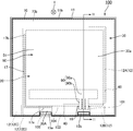
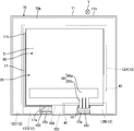
- FIG. 2 is a cross-sectional end view taken along the line II-II in FIG. 1. It is a top view which shows the pattern of the transparent conductive layer in the photoelectric conversion element of FIG. It is a top view which shows the part which removed the protective layer among the photoelectric conversion elements of FIG. It is sectional drawing which shows the state which cut
- FIGS. 1 is a plan view showing an embodiment of the photoelectric conversion element of the present invention
- FIG. 2 is a cross-sectional end view taken along line II-II in FIG. 1
- FIG. 3 is a transparent view of the photoelectric conversion element in FIG. 4 is a plan view showing a pattern of the conductive layer
- FIG. 4 is a plan view showing a part of the photoelectric conversion element of FIG. 1 from which the protective layer is removed
- FIG. 5 is a part of the photoelectric conversion element of FIG. 4 from which the protective layer is removed. It is sectional drawing which shows the state cut
- the photoelectric conversion element 100 includes a transparent substrate 11 having a light receiving surface 11a and one surface of the transparent substrate 11 opposite to the light receiving surface 11a (hereinafter referred to as “cell installation surface”).
- a transparent substrate 11 having a light receiving surface 11a and one surface of the transparent substrate 11 opposite to the light receiving surface 11a (hereinafter referred to as “cell installation surface”).
- One photoelectric conversion cell 20 provided on 11b and a protective layer 30 provided on the cell installation surface 11b side of the transparent substrate 11 and covering and protecting the photoelectric conversion cell 20 are provided.
- a transparent conductive layer 12 is provided on the cell installation surface 11 b of the transparent substrate 11.
- the transparent conductive layer 12 includes an electrode 12A, a conductive first current extraction unit 12B for extracting current from the photoelectric conversion cell 20, and a conductive second current extraction unit 12D for extracting current from the photoelectric conversion cell 20.
- a separation portion 12C provided so as to surround the electrode 12A, the first current extraction portion 12B, and the second current extraction portion 12D.
- the electrode 12A, the first current extraction unit 12B, and the separation unit 12C are disposed in a state of being insulated from each other via the groove 40.
- the electrode 12A and the second current extraction unit 12D are connected to each other.
- the separation portion 12C, the first current extraction portion 12B, and the second current extraction portion 12D are disposed in a state of being insulated from each other via the groove 40.
- the first current extraction portion 12B and the second current extraction portion 12D are also arranged in a state of being insulated from each other so as to be adjacent to each other through the groove 40.
- the photoelectric conversion cell 20 is provided between the transparent substrate 11 and the counter substrate 50, the electrode 12 ⁇ / b> A provided on the cell installation surface 11 b of the transparent substrate 11, the counter substrate 50 facing the electrode 12 ⁇ / b> A.
- an electrolyte 80 to be disposed.
- a first external connection terminal 15a is provided on the first current extraction portion 12B, and is sealed with the first external connection terminal 15a on the first current extraction portion 12B.
- the connection terminal 16 is provided between the unit 60 and the first external connection terminal 15a.
- a second external connection terminal 15b is provided on the second current extraction portion 12D.
- a current collection wiring 17 having a lower resistance than that of the electrode 12A and the second current extraction part 12D is provided so as to straddle the second current extraction part 12D and the electrode 12A.
- first current collector wiring end 17a is located on the second current extraction portion 12D and spaced apart from the second external connection terminal 15b between the second external connection terminal 15b and the sealing portion 60.
- second current collecting wiring end 17b of the current collecting wiring 17 is connected to a position outside the sealing portion 60 on the electrode 12A.
- the counter substrate 50 includes a metal substrate 51 that serves as a substrate and an electrode, and a catalyst layer 52 that is provided on the electrode 12 ⁇ / b> A side of the metal substrate 51 and contributes to the reduction of the electrolyte 80.
- connection terminal 16 and the metal substrate 51 are connected by a conductive member 90.
- the conductive member 90 has a main body portion 90a and at least one (three in the figure) wiring portions 90b that connect the main body portion 90a and the connection terminal 16.
- the insulating layer 70 is an inner insulating layer inside the outer peripheral edge 70 c of the sealing portion 60 when the photoelectric conversion element 100 is viewed in the direction Y orthogonal to the cell installation surface 11 b of the transparent substrate 11. 70 a and an outer insulating layer 70 b outside the outer peripheral edge 70 c of the sealing portion 60.
- the inner insulating layer 70 a is provided in contact with the oxide semiconductor layer 13. That is, the inner insulating layer 70a suppresses intrusion of moisture from the groove 40 into the photoelectric conversion cell 20, so that not only the groove 40 but also the oxide semiconductor layer of the electrode 12A inside the outer peripheral edge 70c of the sealing portion 60 is provided.
- the entire region except the region where 13 is provided is also covered.
- the inner insulating layer 70 a enters the groove 40 in a portion where it overlaps with the groove 40 in order to more sufficiently suppress the intrusion of moisture from the groove 40 into the photoelectric conversion cell 20.
- the outer insulating layer 70b includes a connection terminal-external connection terminal region 101 between the first external connection terminal 15a and the connection terminal 16 in the transparent conductive layer 12, and the second external connection terminal 15b and the first current collector. It is provided so as to cover an area other than the area 102 between the wiring end 17a and the wiring-external connection terminal.
- the region 103 between the external connection terminals between the first external connection terminal 15a and the second external connection terminal 15b in the region outside the sealing portion 60 on the cell installation surface 11b of the transparent substrate 11 is the insulating layer 70.
- the outer insulating layer 70b is covered with the outer insulating layer 70b.
- the region 104 between the connection terminal 16 and the first current collector wiring end 17 a in the region outside the sealing portion 60 on the cell installation surface 11 b of the transparent substrate 11 is also outside the insulating layer 70. It is covered with an insulating layer 70b.
- the protective layer 30 covers not only the photoelectric conversion cell 20 but also the region on the transparent substrate 11 other than the first external connection terminal 15 a and the second external connection terminal 15 b. Covering. That is, the protective layer 30 includes the outer insulating layer 70b of the insulating layer 70, the connection terminal-external connection terminal region 101, the wiring-external connection terminal region 102, the external connection terminal region 103, and the wiring-connection terminal region. 104 is also covered. Moreover, the unevenness
- the photoelectric conversion element 100 when the photoelectric conversion element 100 is viewed in the direction Y perpendicular to the cell installation surface 11 b of the transparent substrate 11, the unevenness 31 is formed on the entire surface 30 a opposite to the transparent substrate 11 of the protective layer 30. Has been. Therefore, irregularities 31 are formed at least in a portion where the protective layer 30 and the counter substrate 50 of the photoelectric conversion cell 20 overlap. For this reason, a surface area becomes large in the whole surface 30a on the opposite side of the transparent substrate 11 of the protective layer 30. Therefore, even when the ambient temperature decreases from a high temperature state, it becomes possible to effectively release the heat of the photoelectric conversion cell 20 from the protective layer 30, and quickly recover the decrease in output due to the temperature increase of the photoelectric conversion cell 20. It becomes possible to do. Therefore, according to the photoelectric conversion element 100, the recoverability of the photoelectric conversion characteristics can be improved when the ambient temperature decreases from the high temperature state.
- the protective layer 30 is in close contact with the metal substrate 51 of the counter substrate 50. That is, there is no air layer between the protective layer 30 and the counter substrate 50. For this reason, compared with the case where the protective layer 30 and the opposing board
- the protective layer 30 is in close contact with the metal substrate 51 having a high thermal conductivity, the heat of the photoelectric conversion cell 20 is higher than that in the case where the protective layer 30 is in close contact with the insulating layer having a relatively low thermal conductivity. Can be transmitted to the protective layer 30 more effectively, and when the ambient temperature falls from a high temperature state, the recovery property of the photoelectric conversion characteristics can be more sufficiently improved.
- the transparent substrate 11, the transparent conductive layer 12, the oxide semiconductor layer 13, the first external connection terminal 15a, the second external connection terminal 15b, the connection terminal 16, the current collector wiring 17, the dye, the protective layer 30, and the counter substrate 50 The sealing part 60, the insulating layer 70, the electrolyte 80, and the conductive member 90 will be described in detail.
- the material which comprises the transparent substrate 11 should just be a transparent material, for example, as such a transparent material, glass, such as borosilicate glass, soda lime glass, white plate glass, quartz glass, polyethylene terephthalate (PET), for example , Polyethylene naphthalate (PEN), polycarbonate (PC), and polyethersulfone (PES).
- PET polyethylene terephthalate
- PEN Polyethylene naphthalate
- PC polycarbonate
- PES polyethersulfone
- the thickness of the transparent substrate 11 is appropriately determined according to the size of the photoelectric conversion element 100 and is not particularly limited, but may be in the range of 0.05 to 10 mm, for example.
- Transparent conductive layer examples of the material contained in the transparent conductive layer 12 include conductive metal oxides such as tin-added indium oxide (ITO), tin oxide (SnO 2 ), and fluorine-added tin oxide (FTO).
- the transparent conductive layer 12 may be a single layer or a laminate of a plurality of layers containing different conductive metal oxides. When the transparent conductive layer 12 is composed of a single layer, the transparent conductive layer 12 preferably includes FTO because it has high heat resistance and chemical resistance.
- the transparent conductive layer 12 may further include a glass frit.
- the thickness of the transparent conductive layer 12 may be in the range of 0.01 to 2 ⁇ m, for example.
- the oxide semiconductor layer 13 is composed of oxide semiconductor particles.
- the oxide semiconductor particles include titanium oxide (TiO 2 ), silicon oxide (SiO 2 ), zinc oxide (ZnO), tungsten oxide (WO 3 ), niobium oxide (Nb 2 O 5 ), and strontium titanate (SrTiO 3 ).
- the oxide semiconductor layer 13 is usually composed of an absorption layer for absorbing light, but may be composed of an absorption layer and a reflection layer that reflects light transmitted through the absorption layer and returns it to the absorption layer.
- the thickness of the oxide semiconductor layer 13 is not particularly limited, but is usually 0.5 to 50 ⁇ m.
- the first external connection terminal 15a and the second external connection terminal 15b include a metal material.
- the metal material include silver, copper, and indium. You may use these individually or in combination of 2 or more types.
- the 1st external connection terminal 15a and the 2nd external connection terminal 15b are comprised by the sintered compact which consists only of metal materials, for example.
- connection terminal 16 includes a metal material.
- the connection terminal 16 may be made of the same material as the first external connection terminal 15a and the second external connection terminal 15b or may be made of a different material, but is preferably made of the same material.
- the current collection wiring 17 contains a metal material.
- the current collecting wiring 17 may be made of the same material as the first external connection terminal 15a and the second external connection terminal 15b or may be made of a different material, but is preferably made of the same material.
- the dye examples include photosensitizing dyes such as ruthenium complexes having a ligand containing a bipyridine structure, a terpyridine structure, etc., organic dyes such as porphyrin, eosin, rhodamine and merocyanine, and organic-types such as lead halide perovskite crystals.
- photosensitizing dyes such as ruthenium complexes having a ligand containing a bipyridine structure, a terpyridine structure, etc.
- organic dyes such as porphyrin, eosin, rhodamine and merocyanine
- organic-types such as lead halide perovskite crystals.
- examples include inorganic composite dyes.
- the photoelectric conversion element 100 becomes a dye-sensitized photoelectric conversion element
- a photosensitizing dye comprising a ruthenium complex having a ligand containing a bipyridine structure or a terpyridine structure is preferable.
- the photoelectric conversion characteristics of the photoelectric conversion element 100 can be further improved.
- the unevenness 31 is formed on the surface 30a of the protective layer 30 opposite to the transparent substrate 11.
- the degree of unevenness of the unevenness 31 of the protective layer 30 is not particularly limited, but the unevenness 31 is preferably an unevenness having an arithmetic average roughness Ra of 0.2 ⁇ m or more. In this case, the surface area becomes wider as compared with the case where the irregularities 31 are irregularities having an arithmetic average roughness Ra of less than 0.2 ⁇ m. Therefore, even when the ambient temperature decreases from a high temperature state, the heat of the photoelectric conversion cell 20 can be more effectively released from the protective layer 30, and the output decrease due to the temperature increase of the photoelectric conversion cell 20 can be promptly performed. It becomes possible to recover. Therefore, according to the photoelectric conversion element 100, the recoverability of the photoelectric conversion characteristics can be further improved when the ambient temperature decreases from the high temperature state.
- the irregularities 31 are more preferably irregularities having an arithmetic average roughness Ra of 0.3 ⁇ m or more. In this case, it becomes easier for the protective layer 30 to radiate heat, and it becomes possible to more quickly recover the decrease in output due to the temperature increase of the photoelectric conversion cell 20.
- the irregularities 31 are preferably irregularities having an arithmetic average roughness Ra of 15 ⁇ m or less.
- the photoelectric conversion element 100 is incorporated in a housing (not shown), and the housing and the photoelectric conversion element 100 are protected.
- the contact area between the housing and the protective layer 30 of the photoelectric conversion element 100 becomes larger. For this reason, it becomes possible to discharge
- the irregularities 31 are more preferably irregularities having an arithmetic average roughness Ra of 10 ⁇ m or less.
- the unevenness 31 may be formed by regularly arranging at least one of a recess having the same depth and a protrusion having the same height. it can. In this case, the surface area can be increased, and the heat generated in the photoelectric conversion cell 20 can be released more effectively.
- the protective layer 30 usually has a layer (resin layer) made of a resin material (insulating material) on the transparent substrate 11 side.
- the protective layer 30 may be composed of, for example, at least one layer (resin layer) made of a resin material, or a laminate including a resin layer and a layer (metal layer) made of a metal material. Also good.
- the resin material include polyimide resin, epoxy resin, polyurethane resin, and polyethylene terephthalate (PET) resin.
- polyimide resin is preferred.
- the resin layer includes a polyimide resin having excellent insulating properties, more excellent insulating properties can be imparted to the protective layer 30.
- the polyimide resin has a smaller linear expansion coefficient than the insulating plastic material other than the polyimide resin, the linear expansion coefficient of the resin layer is also smaller than that of the insulating plastic material other than the polyimide resin.
- the metal substrate 51 included in the counter substrate 50 also has a smaller linear expansion coefficient than the insulating plastic material other than the polyimide resin.
- the resin layer easily follows the metal substrate 51 even in an environment where the temperature change is large, the shear stress applied between the resin layer and the metal substrate 51 can be reduced, and the resin layer is made of metal. Separation from the substrate 51 is sufficiently suppressed. Furthermore, since the polyimide resin has a lower dielectric constant than the metal layer, the protective layer 30 short-circuits the metal substrate 51 of the counter substrate 50 and the electrode 12A unlike the case where a metal layer is used instead of the resin layer. Can be more sufficiently suppressed.
- the resin layer of the protective layer 30 may be in close contact with the conductive member 90 connected to the metal substrate 51 as shown in FIG.
- the conductive member 90 also has a smaller linear expansion coefficient than the insulating plastic material other than the polyimide resin, like the metal substrate 51 included in the counter substrate 50. For this reason, even in an environment with a large temperature change, the resin layer easily follows the conductive member 90, and the conductive member 90 is sufficiently suppressed from being pulled and cut by the resin layer.
- examples of the metal material include aluminum and stainless steel.
- the protective layer 30 is in direct contact with the metal substrate 51 of the counter substrate 50 in FIG. 2, the protective layer 30 may be in intimate contact with the metal substrate 51 of the counter substrate 50 via an adhesive. .
- the color of the protective layer 30 is not particularly limited, but is preferably black. In this case, heat radiation becomes particularly large, and heat generated in the photoelectric conversion cell 20 is easily released, so that the protective layer 30 can release heat more effectively. Therefore, according to the photoelectric conversion element 100, the recoverability of the photoelectric conversion characteristics can be further improved when the ambient temperature decreases from the high temperature state.
- the thickness of the protective layer 30 is not particularly limited, but is preferably 30 to 300 ⁇ m. In this case, the heat resistance of the protective layer 30 becomes higher.
- the counter substrate 50 includes the metal substrate 51 serving as a substrate and an electrode, and the catalyst layer 52.
- the metal substrate 51 should just be comprised with a metal, it is preferable that this metal is a metal which can form a passive state. In this case, since the metal substrate 51 is less likely to be corroded by the electrolyte 80, the photoelectric conversion element 100 can have more excellent durability.
- the metal capable of forming a passive material include titanium, nickel, molybdenum, tungsten, aluminum, stainless steel, and alloys thereof.
- the thickness of the metal substrate 51 is appropriately determined according to the size of the photoelectric conversion element 100 and is not particularly limited, but may be, for example, 0.005 to 0.1 mm.
- the catalyst layer 52 is composed of platinum, a carbon-based material, a conductive polymer, or the like.
- carbon black and carbon nanotubes are preferably used as the carbon-based material.
- the material constituting the sealing portion 60 examples include an ionomer, an ethylene-vinyl acetate anhydride copolymer, an ethylene-methacrylic acid copolymer, an ethylene-vinyl alcohol copolymer, a modified polyolefin resin, an ultraviolet curable resin, And resin, such as a vinyl alcohol polymer, is mentioned. These resins can be used alone or in combination of two or more.
- the thickness of the sealing part 60 is not particularly limited, but is usually 10 to 50 ⁇ m, preferably 20 to 40 ⁇ m. In this case, the penetration of water into the inside of the sealing portion 60 can be more sufficiently suppressed.
- the insulating layer 70 only needs to be made of an insulating material.
- an insulating material include a resin and an inorganic insulating material, and among them, an inorganic insulating material is preferable.
- the insulating layer 70 covers not only the groove 40 inside the outer peripheral edge 70c of the sealing portion 60 but also the entire region excluding the region where the oxide semiconductor layer 13 is provided in the electrode 12A. Since the material has a higher sealing ability than the resin, the intrusion of moisture from the groove 40 can be more sufficiently suppressed.
- An example of such an inorganic insulating material is glass.
- the insulating material constituting the insulating layer 70 is preferably colored. In this case, when the photoelectric conversion element 100 is viewed from the light receiving surface 11a side, it is possible to sufficiently suppress the counter substrate 50 from being noticeable. For this reason, a favorable external appearance can be realized. Moreover, since it is not necessary to color electrode 12A, the fall of the photoelectric conversion characteristic of the photoelectric conversion element 100 can fully be suppressed.
- the colored insulating material for example, an inorganic insulating material such as colored glass is used.
- the color of the insulating layer 70 is not particularly limited, and various colors can be used according to the purpose.
- the thickness of the insulating layer 70 is not particularly limited, but is usually 10 to 30 ⁇ m, preferably 15 to 25 ⁇ m.
- the electrolyte 80 includes a redox couple and an organic solvent.
- organic solvent acetonitrile, methoxyacetonitrile, methoxypropionitrile, propionitrile, ethylene carbonate, propylene carbonate, diethyl carbonate, ⁇ -butyrolactone, valeronitrile, pivalonitrile and the like can be used.
- the redox pair include iodide ions / polyiodide ions (for example, I ⁇ / I 3 ⁇ ), and redox pairs such as bromide ions (bromine ions) / polybromide ions, zinc complexes, iron complexes, and cobalt complexes.
- the iodide ion / polyiodide ion can be formed by iodine (I 2 ) and a salt (ionic liquid or solid salt) containing iodide (I ⁇ ) as an anion.
- iodine I 2
- a salt ionic liquid or solid salt
- I ⁇ iodide
- an anion such as LiI or tetrabutylammonium iodide is used.
- a salt containing iodide (I ⁇ ) may be added.
- the electrolyte 80 may be an ionic liquid instead of an organic solvent.
- the ionic liquid for example, a known iodine salt such as a pyridinium salt, an imidazolium salt, or a triazolium salt, and a room temperature molten salt that is in a molten state near room temperature is used.
- room temperature molten salts include 1-hexyl-3-methylimidazolium iodide, 1-ethyl-3-propylimidazolium iodide, dimethylimidazolium iodide, ethylmethylimidazolium iodide, and dimethylpropyl.
- Imidazolium iodide, butylmethylimidazolium iodide, or methylpropyl imidazolium iodide is preferably used.
- the electrolyte 80 may be a mixture of the ionic liquid and the organic solvent instead of the organic solvent.
- An additive can be added to the electrolyte 80.
- the additive include LiI, I 2 , 4-t-butylpyridine, guanidinium thiocyanate, 1-methylbenzimidazole, 1-butylbenzimidazole and the like.
- a nanocomposite gel electrolyte which is a pseudo-solid electrolyte obtained by kneading nanoparticles such as SiO 2 , TiO 2 , and carbon nanotubes with the electrolyte, may be used, or polyvinylidene fluoride.
- an electrolyte gelled with an organic gelling agent such as a polyethylene oxide derivative or an amino acid derivative may be used.
- Electrolyte 80 preferably includes an oxidation-reduction pair consisting of iodide ions / polyiodide ions (for example, I ⁇ / I 3 ⁇ ), and the concentration of polyiodide ions is preferably 0.006 mol / liter or less.
- the concentration of polyiodide ions that carry electrons is low, the leakage current can be further reduced. For this reason, since an open circuit voltage can be increased more, a photoelectric conversion characteristic can be improved more.
- the concentration of polyiodide ions is preferably 0.005 mol / liter or less, more preferably 0 to 6 ⁇ 10 ⁇ 6 mol / liter, and 0 to 6 ⁇ 10 ⁇ 8 mol / liter. Is more preferable.
- the color of the electrolyte 80 can be made inconspicuous.
- the conductive member 90 includes a metal material.
- the metal material for example, silver or copper can be used.
- the conductive member 90 may further include a binder resin in addition to the metal material.
- the binder resin include an epoxy resin, a polyester resin, and an acrylic resin. Of these, epoxy resins and polyester resins are preferred because they are less likely to thermally expand even at high temperatures and the resistance change with time can be further reduced.
- the conductive member 90 includes the main body portion 90a and the wiring portion 90b.
- the main body portion 90a of the conductive member 90 may be formed of a laminate having a first layer directly connected to the metal substrate 51 and a second layer provided on the first layer.
- the first layer includes a metal material, a binder resin, and carbon
- the second layer includes a metal material and a binder resin
- the carbon content in the first layer is the carbon content in the second layer. It is preferable that it is larger than the rate. In this case, the conductive member 90 is difficult to peel from the metal substrate 51.
- FIG. 6 is a cross-sectional view showing a structure obtained in the middle of the method for manufacturing the photoelectric conversion element of FIG.
- a laminate formed by forming a transparent conductive film on the cell installation surface 11b of one transparent substrate 11 is prepared.
- the transparent conductive film As a method for forming the transparent conductive film, sputtering, vapor deposition, spray pyrolysis, CVD, or the like is used.
- the groove 40 is formed in the transparent conductive film, and the transparent conductive layer 12 is formed.
- the transparent conductive layer 12 is formed such that the electrode 12A, the first current extraction unit 12B, the separation unit 12C, and the second current extraction unit 12D are formed.
- the groove 40 can be formed by a laser scribing method using, for example, a YAG laser or a CO 2 laser as a light source.
- a precursor of the first external connection terminal 15a and a precursor of the connection terminal 16 are formed on the first current extraction portion 12B.
- the precursor of the first external connection terminal 15a and the precursor of the connection terminal 16 can be formed, for example, by applying a silver paste and drying.
- a precursor of the second external connection terminal 15b is formed on the second current extraction portion 12D.
- the precursor of the second external connection terminal 15b can be formed, for example, by applying a silver paste and drying it.
- the precursor of the current collecting wiring 17 is formed so as to straddle the electrode 12A and the second current extraction portion 12D. At this time, one end of the current collecting wiring 17 is disposed on the second current extraction portion 12D at a position separated from the precursor of the second external connection terminal 15b, and the other end is disposed on the electrode 12A. It is formed to be arranged.
- the precursor of the current collecting wiring 17 can be formed, for example, by applying a silver paste and drying it.
- a region where the oxide semiconductor layer 13 is to be formed (hereinafter referred to as "semiconductor layer formation planned region"), a region 101 between the connection terminal and the external connection terminal, and a wiring and the outside
- the precursor of the insulating layer 70 is formed so as to cover a region other than the connection terminal region 102. At this time, the precursor of the insulating layer 70 is formed so that the precursor of the insulating layer 70 enters the groove 40.
- the precursor of the insulating layer 70 can be formed, for example, by applying and drying a paste containing an inorganic insulating material.
- the precursor of the first external connection terminal 15a, the precursor of the second external connection terminal 15b, the precursor of the connection terminal 16, the precursor of the current collecting wiring 17, and the precursor of the insulating layer 70 are baked together.
- the first external connection terminal 15a, the second external connection terminal 15b, the connection terminal 16, the current collecting wiring 17 and the insulating layer 70 are formed.
- the firing temperature varies depending on the type of insulating material, etc., it is usually 350 to 600 ° C., and the firing time also varies depending on the type of insulating material, but is usually 1 to 5 hours.
- a precursor of the oxide semiconductor layer 13 is formed on the semiconductor layer formation scheduled region of the electrode 12A.
- the precursor of the oxide semiconductor layer 13 is obtained by printing and drying an oxide semiconductor layer paste for forming the oxide semiconductor layer 13.
- the oxide semiconductor layer paste includes, for example, titanium oxide, a resin such as polyethylene glycol and ethyl cellulose, and a solvent such as terpineol.
- a method for printing the oxide semiconductor layer paste for example, a screen printing method, a doctor blade method, a bar coating method, or the like can be used.
- the precursor of the oxide semiconductor layer 13 is baked to form the oxide semiconductor layer 13.
- the firing temperature varies depending on the type of oxide semiconductor particles, etc., it is usually 350 to 600 ° C., and the firing time also varies depending on the type of oxide semiconductor particles, but is usually 1 to 5 hours.
- the sealing part forming body can be obtained, for example, by preparing one sealing resin film made of a material constituting the sealing part 60 and forming an opening in the sealing resin film.
- this sealing part formation body is adhere
- the sealing portion forming body is bonded to the structure A so as to overlap with the insulating layer 70 and the oxide semiconductor layer 13 is disposed inside. Adhesion of the sealing portion forming body to the structure A can be performed by, for example, heating and melting the sealing portion forming body.
- a dye is supported on the oxide semiconductor layer 13 of the structure A.
- the structure A is immersed in a dye solution containing a dye, the dye is adsorbed on the oxide semiconductor layer 13, and then the excess dye is washed away with the solvent component of the solution and dried. Just do it.
- the electrolyte 80 is disposed on the oxide semiconductor layer 13.
- the counter substrate 50 can be obtained, for example, by forming a conductive catalyst layer 52 on the metal substrate 51.
- the sealing portion forming body bonded to the counter substrate 50 and the sealing portion forming body bonded to the structure A in which the electrolyte 80 is arranged are overlapped, and the sealing portion forming body is heated and melted while being pressurized. .
- the sealing portion 60 is formed between the transparent substrate 11 and the counter substrate 50 of the structure A.
- the formation of the sealing portion 60 may be performed under atmospheric pressure or under reduced pressure, but is preferably performed under reduced pressure.
- the connection terminal 16 and the metal substrate 51 of the counter substrate 50 are connected by the conductive member 90.
- the conductive member 90 prepares a paste containing a metal material constituting the conductive member 90, and applies and cures this paste so as to connect the metal substrate 51 of the counter substrate 50 and the connection terminal 16.
- the paste it is preferable to use a low-temperature curable paste that can be cured at a temperature of 90 ° C. or lower from the viewpoint of avoiding adverse effects on the dye supported on the oxide semiconductor layer 13.
- the protective layer 30 is formed.
- the protective layer 30 can be obtained, for example, by forming the protective layer 30 and applying and heating a paste containing a resin material. At this time, the degree of the unevenness 31 can be adjusted by appropriately changing the mixing ratio of components (for example, matting agent) in the paste. Or after preparing the precursor of the protective layer 30, forming the unevenness
- the peripheral edge portion 30A of the precursor is adhered to the outer insulating layer 70b of the insulating layer 70, and the protective layer 30 and the counter substrate 50 are brought into close contact with each other.
- the precursor of the protective layer 30 is formed so as to cover not only the photoelectric conversion cell 20 but also the region on the transparent substrate 11 other than the first external connection terminal 15a and the second external connection terminal 15b.
- the protective layer 30 includes not only the photoelectric conversion cell 20 but also the outer insulating layer 70b of the insulating layer 70, the connection terminal-external connection terminal region 101, the wiring-external connection terminal region 102, the external connection terminal region 103, Further, the wiring-connection terminal region 104 is also formed so as to cover it.
- the photoelectric conversion element 100 is obtained as described above (see FIG. 1).
- the present invention is not limited to the above embodiment.
- the unevenness 31 is formed on the entire surface 30a opposite to the transparent substrate 11 of the protective layer 30, but the unevenness 31 is not necessarily formed on the surface 30a opposite to the transparent substrate 11 of the protective layer 30. It does not have to be formed entirely.
- the protective layer 30 is viewed in the direction Y orthogonal to the cell placement surface 11b of the transparent substrate 11, the unevenness 31 is formed on the surface 30a of the protective layer 30 opposite to the transparent substrate 11 and the protective layer 30 and the counter substrate 50. Should just be formed at least in the overlapping part.
- the protective layer 30 and the counter substrate 50 are in close contact, but the protective layer 30 and the counter substrate 50 do not necessarily have to be in close contact. That is, the protective layer 30 and the counter substrate 50 may be separated from each other. In other words, an air layer may be provided between the protective layer 30 and the counter substrate 50.
- the protective layer 30 is not limited to the photoelectric conversion cell 20, but the outer insulating layer 70b of the insulating layer 70, the connection terminal-external connection terminal region 101, the wiring-external connection terminal region 102, the external connection.
- the inter-terminal region 103 and the wiring-connection terminal region 104 are also covered, but the portions other than the photoelectric conversion cell 20 may not be covered.
- the outer insulating layer 70b of the insulating layer 70 includes the connection terminal-external connection terminal region 101 in the transparent conductive layer 12 between the sealing portion 60 and the peripheral portion of the transparent substrate 11, and The area other than the area 102 between the wiring and the external connection terminals is provided so as to cover the area, but the area 101 between the connection terminals and the external connection terminals and the area 102 between the wiring and the external connection terminals may also be covered. .
- the insulating layer 70 covers the entire region of the electrode 12A excluding the region where the oxide semiconductor layer 13 is provided inside the outer peripheral edge 70c of the sealing portion 60. 70 may cover only a part of the electrode 12 ⁇ / b> A inside the outer peripheral edge 70 c of the sealing portion 60. Moreover, in the said embodiment, although the insulating layer 70 is comprised by the inner side insulating layer 70a and the outer side insulating layer 70b, the insulating layer 70 may be comprised only by the inner side insulating layer 70a.
- the photoelectric conversion element 100 has the insulating layer 70, it does not need to have the insulating layer 70.
- FIG. 1 is a diagrammatic representation of the photoelectric conversion element 100.
- the photoelectric conversion element 100 has the current collection wiring 17.
- the photoelectric conversion element of the present invention does not necessarily have the current collection wiring 17.
- the counter substrate 50 includes the metal substrate 51 serving as both a substrate and an electrode.
- the counter substrate 50 may include a conductive substrate instead of the metal substrate 51.
- the conductive substrate may be composed of a transparent substrate 11 and an electrode provided between the transparent substrate 11 and the catalyst 22 by separating the substrate and the electrode.
- the electrode is made of a conductive oxide such as ITO or FTO.
- the counter substrate 50 includes the metal substrate 51 and the catalyst layer 52.
- the counter substrate 50 may be formed of an insulating substrate.
- a laminate composed of the oxide semiconductor layer 13, the porous insulating layer impregnated with the electrolyte 80, and the counter electrode is sequentially provided between the electrode 12A and the counter substrate 50 from the electrode 12A side. It is done.
- the separation part 12C is provided on the transparent substrate 11 so as to surround the electrode 12A and the second current extraction part 12B, but the separation part 12C is not provided on the transparent substrate 11. Also good.
- the photoelectric conversion cell 20 is provided on the transparent substrate 11, but in the photoelectric conversion element 100, a plurality of photoelectric conversion cells 20 may be provided on the transparent substrate 11.
- at least the unevenness 31 needs to be formed in a portion of the surface 30 a opposite to the transparent substrate 11 of the protective layer 30 that overlaps the counter substrate 50 of the plurality of photoelectric conversion cells 20.
- the several photoelectric conversion cell 20 may be connected in series, and may be connected in parallel.
- Example 1 First, a laminate was prepared by forming a transparent conductive film made of FTO having a thickness of 0.7 ⁇ m on a transparent substrate made of alkali-free glass and having a size of 112 mm ⁇ 56 mm and a thickness of 2.2 mm. Next, as shown in FIG. 3, a groove 40 was formed in the transparent conductive film by a YAG laser, and the transparent conductive layer 12 was formed. At this time, the transparent conductive layer 12 was formed such that the electrode 12A, the first current extraction unit 12B, the separation unit 12C, and the second current extraction unit 12D were formed. At this time, the width of the groove 40 was set to 0.1 mm.
- the electrode 12A was formed to have a square shape of 54.4 mm ⁇ 104.5 mm, and the second current extraction portion 12D was formed to extend from one side of the electrode 12A to have a square shape.
- the length in the extending direction of the second current extraction portion 12D was 4.3 mm, and the width of the second current extraction portion 12D was 27.2 mm.
- the first current extraction portion 12B was formed to have a size of 27.2 mm ⁇ 4.3 mm.
- the precursor of the first external connection terminal 15a and the precursor of the connection terminal 16 were formed in a rectangular shape and spaced apart from each other on the first current extraction portion 12B. At this time, the precursor of the first external connection terminal 15a was formed to have a size of 8 mm ⁇ 1.8 mm, and the precursor of the connection terminal 16 was formed to have a size of 8 mm ⁇ 0.3 mm.
- a precursor of the second external connection terminal 15b was formed in a rectangular shape on the second current extraction portion 12D. At this time, the precursor of the second external connection terminal 15b was formed to have a size of 8 mm ⁇ 1.8 mm.
- the current collection wiring 17 was formed so as to straddle the second current extraction part 12D and the electrode 12A. At this time, one end of the precursor of the current collector wiring 17 is disposed on the second current extraction portion 12D at a position separated from the precursor of the second external connection terminal 15b, and the other end is on the electrode 12A. It was formed so as to be arranged at the position.
- the current collector wiring precursor has an L-shape and a portion having a width of 0.3 mm ⁇ a length of 21.6 mm and a portion having a width of 0.3 mm ⁇ a length of 105.1 mm. Formed.
- the precursor of the connection terminal 16, the precursor of the first external connection terminal 15a, the precursor of the second external connection terminal 15b, and the precursor of the current collector wiring 17 are all formed by applying a silver paste and drying. did.
- the precursor of the insulating layer 70 so as to cover the region other than the region where the semiconductor layer is to be formed, the region 101 between the connection terminal and the external connection terminal, and the region 102 between the wiring and the external connection terminal Formed.
- the precursor of the insulating layer 70 was formed so as to enter the groove 40.
- the precursor of the insulating layer 70 was formed by applying and drying a paste containing glass frit (trade name “PLFOC-837B”, manufactured by Okuno Pharmaceutical Co., Ltd.).
- the precursor of the first external connection terminal 15a, the precursor of the second external connection terminal 15b, the precursor of the connection terminal 16, the precursor of the current collecting wiring 17, and the precursor of the insulating layer 70 are baked together.
- the first external connection terminal 15a, the second external connection terminal 15b, the connection terminal 16, the current collector wiring 17, and the insulating layer 70 were formed.
- the firing temperature was 500 ° C.
- the firing time was 1 hour.
- the distance L between the first external connection terminal 15a and the connection terminal 16 was 0.5 mm.
- the distance L ′ between the second external connection terminal 15b and the first current collector wiring end 17a was 0.5 mm.
- a precursor of the oxide semiconductor layer 13 was formed on the semiconductor layer formation scheduled region of the electrode 12A.
- the precursor of the oxide semiconductor layer 13 was obtained by applying a paste containing titanium oxide so as to fill the inside of the insulating layer 70 by screen printing and drying at 150 ° C. for 10 minutes.
- the precursor of the oxide semiconductor layer 13 was fired to form the oxide semiconductor layer 13.
- the firing temperature was 500 ° C.
- the firing time was 1 hour.
- the sealing part forming body is prepared by preparing a sealing resin film made of 51.2 mm ⁇ 106.1 mm ⁇ 35 ⁇ m maleic anhydride-modified polyethylene (trade name “Binell”, manufactured by DuPont). It was obtained by forming one rectangular opening of 47.2 mm ⁇ 102.1 mm in the resin film for use.
- this sealing part formation body was piled up on structure A, it was made to adhere to insulating layer 70 on structure A by heating and melting the sealing part formation body. At this time, the sealing portion formation body was adhered to the structure A so as to overlap the insulating layer 70 and to be disposed between the oxide semiconductor layer 13, the connection terminal 16, and the current collector wiring 17.
- the structure A obtained as described above is mixed by containing 0.2 mM of a photosensitizing dye composed of Z907, mixing a solvent with acetonitrile and tert-butanol at a volume ratio of 1: 1. After being immersed in a dye solution as a solvent for a whole day and night, it was taken out and dried, and a photosensitizing dye was supported on the oxide semiconductor layer.
- an electrolyte 80 obtained by adding I 2 , methylbenzimidazole, butylbenzimidazole, guanidinium thiocyanate and t-butylpyridine was prepared.
- the electrolyte 80 was dropped onto the oxide semiconductor layer 13, applied, and dried to place the electrolyte 80.
- the counter substrate 50 was prepared by forming a catalyst layer made of platinum having a thickness of 5 nm on a 51.2 mm ⁇ 106.1 mm ⁇ 40 ⁇ m titanium foil by sputtering.
- another sealing part forming body was prepared. And the opposing board
- positioned are piled up under reduced pressure, and it heats, pressurizing a sealing part formation body Melted.
- a sealing portion was formed between the structure A and the counter substrate.
- the thickness of the sealing part was 40 ⁇ m, and the width of the sealing part was 2 mm.
- connection terminal 16 and the metal substrate 51 of the counter substrate 50 were connected by the conductive member 90 as follows.
- silver particles (average particle size: 3.5 ⁇ m), carbon (average particle size: 500 nm), and polyester resin were dispersed in a solvent composed of diethylene glycol monoethyl ether acetate to prepare a first conductive paste.
- the silver particles, carbon, polyester resin, and solvent were mixed at a mass ratio of 70: 1: 10: 19.
- silver particles (average particle size: 2 ⁇ m) and polyester resin were dispersed in a solvent composed of ethylene glycol monobutyl ether to prepare a second conductive paste.
- the silver particles, the polyester resin, and the solvent were mixed at a mass ratio of 65:10:25.
- the said 1st conductive paste was apply
- the main body 90a is formed to have a size of 41.2 mm ⁇ 4.5 mm ⁇ thickness 60 ⁇ m, and the three wiring portions 90b each have a size of 2 mm ⁇ 4.7 mm ⁇ thickness 30 mm. Formed as follows.
- thermocouple (trade name “Super Extrafine-005-K”, manufactured by Ninomiya Electric Cable Co., Ltd.) was attached to the metal substrate 51 of the counter substrate 50.
- a matte agent (trade name “Techpolymer”, manufactured by Sekisui Chemical Co., Ltd.) is added to a paint containing acrylic urethane resin (trade name “RECRACK 110”, manufactured by Fujikura Kasei Co., Ltd.) with an arithmetic average roughness Ra of 0.
- a paste mixed at a mixing ratio of 0.7 ⁇ m was prepared, and this paste was applied so as to cover the photoelectric conversion cell 20 to form a precursor of the protective layer 30.
- the precursor of the protective layer 30 was formed so as to cover the ultrafine thermocouple.
- corrugation 31 was formed in the whole surface 30a on the opposite side to the transparent substrate 11 among the precursors of the protective layer 30 by heating in 80 degreeC oven for 30 minutes.
- the protective layer 30 was formed so as to cover not only the photoelectric conversion cell 20 but also the region on the transparent substrate 11 other than the first external connection terminal 15a and the second external connection terminal 15b. That is, the protective layer 30 includes not only the photoelectric conversion cell 20 but also the outer insulating layer 70b of the insulating layer 70, the connection terminal-external connection terminal region 101, the wiring-external connection terminal region 102, the external connection terminal region 103, In addition, the wiring-connection terminal region 104 is also formed so as to cover it.
- the photoelectric conversion element 100 was obtained as described above.
- Example 1 except that the paste was prepared by mixing the matting agent with the blending ratio of arithmetic average roughness Ra as shown in Table 1 and the protective layer 30 was formed using the paste. Similarly, a photoelectric conversion element was produced.
- Example 4 A back sheet (total thickness: 88 ⁇ m) composed of a laminate of a first resin layer made of acrylic urethane resin having a thickness of 20 ⁇ m, an aluminum foil having a thickness of 30 ⁇ m, and a second resin layer having a thickness of 38 ⁇ m made of polyethylene terephthalate.
- a photoelectric conversion element was produced in the same manner as in Example 1 except that an air layer having a thickness of 2 mm was provided between the protective layer 30 and the counter substrate 50 as a protective layer.
- the first resin layer is prepared by preparing a paste in which the matting agent is mixed with the paint at a mixing ratio such that the arithmetic average roughness Ra is as shown in Table 2, and the paste is 30 in an oven at 80 ° C. It was prepared by forming the irregularities 31 on the entire surface 30a opposite to the aluminum foil of the first resin layer by partial heating.
- Examples 5 to 6 and Comparative Example 2 The same as in Example 4 except that the first resin layer of the back sheet was formed using a paste in which the matting agent was mixed with the coating material at a mixing ratio such that the arithmetic average roughness Ra is as shown in Table 2. Thus, a photoelectric conversion element was produced.
- Example 7 As a protective layer, a laminate of a first resin layer made of acrylic urethane resin having a thickness of 20 ⁇ m and a second resin layer made of polyimide film having a thickness of 50 ⁇ m (linear expansion coefficient: 27 ppm / ° C.) was used. The acrylic adhesive is adhered so as to cover regions other than the first external connection terminal 15a and the second external connection terminal 15b in the regions on the photoelectric conversion cell 20 and the transparent substrate 11, and is opposite to the transparent substrate of the protective layer.
- a photoelectric conversion element was produced in the same manner as in Example 1 except that irregularities were formed on the entire surface and the arithmetic average roughness Ra on the surface was set to the values shown in Table 3.
- Example 8 A first resin layer made of acrylic urethane resin having a thickness of 20 ⁇ m, a second resin layer having a thickness of 55 ⁇ m made of linear low density polyethylene (LLDPE), and an aluminum foil having a thickness of 20 ⁇ m (linear expansion coefficient: 24 ppm / ° C. ) And a back sheet (total thickness: 150 ⁇ m) made of a laminate of a 55 ⁇ m thick third resin layer made of linear low density polyethylene (LLDPE) as a protective layer and opposite to the transparent substrate of the protective layer
- LLDPE linear low density polyethylene
- Example 9 As the protective layer, a laminate of a first resin layer made of an acrylic urethane resin having a thickness of 20 ⁇ m and a second resin layer made of a polyethylene terephthalate (PET) film having a thickness of 50 ⁇ m (linear expansion coefficient: 65 ppm / ° C.) is used.
- the laminated body is adhered with an acrylic adhesive so as to cover regions other than the first external connection terminal 15a and the second external connection terminal 15b in the regions on the photoelectric conversion cell 20 and the transparent substrate 11, and the protective layer.
- a photoelectric conversion element was produced in the same manner as in Example 1 except that irregularities were formed on the entire surface opposite to the transparent substrate, and the arithmetic average roughness Ra on the surface was set to the values shown in Table 3.
Landscapes
- Engineering & Computer Science (AREA)
- Power Engineering (AREA)
- Microelectronics & Electronic Packaging (AREA)
- Hybrid Cells (AREA)
- Photovoltaic Devices (AREA)
Abstract
透明基板と、透明基板の一面上に設けられる少なくとも1つの光電変換セルと、透明基板の一面側に設けられ、光電変換セルを覆って保護する保護層とを備える光電変換素子が開示されている。光電変換セルは、透明基板の一面上に設けられる電極と、電極に対向する対向基板とを備えている。光電変換素子においては、光電変換素子を透明基板の一面に直交する方向に見た場合、保護層の透明基板と反対側の面のうち、少なくとも保護層と光電変換セルの対向基板とが重なり合う部分に凹凸が形成されている。
Description
本発明は、光電変換素子に関する。
光電変換素子として、安価で、高い光電変換効率が得られることから色素を用いた光電変換素子が注目されており、色素を用いた光電変換素子に関して種々の開発が行われている。
色素を用いた光電変換素子は一般に、透明基板と、透明基板の一面上に設けられる少なくとも1つの光電変換セルとを備えており、光電変換セルは、透明基板上に設けられる電極と、電極に対向する対極などの対向基板と、電極と対向基板との間に設けられる酸化物半導体層と、酸化物半導体層に担持される色素とを備えている。
このような色素を用いた光電変換素子としては、例えば下記特許文献1に記載の色素増感型太陽電池素子が知られている。下記特許文献1には、透明基板上に、光電変換セルを覆うように設けられるバックシートを備えた色素増感太陽電池素子が開示されている。
しかし、上記特許文献1に記載の色素増感太陽電池素子は以下に示す課題を有していた。
すなわち、上記特許文献1に記載の色素増感太陽電池素子は、周囲の温度が高温状態から低下する場合における光電変換特性の回復性の向上の点で改善の余地があった。
本発明は上記事情に鑑みてなされたものであり、周囲の温度が高温状態から低下する場合に、光電変換特性の回復性を向上させることができる光電変換素子を提供することを目的とする。
まず本発明者らは、上記特許文献1の色素増感太陽電池素子において、上記課題が生じる原因について検討した。その結果、上記特許文献1の色素増感太陽電池素子において、周囲の温度が高温状態になり、光電変換セルの温度が上昇した場合に、その光電変換セルの熱が、光電変換セルを覆っているバックシートから放熱されにくいことが、上記課題が生じる原因ではないかと本発明者らは考えた。そこで、本発明者らはさらに鋭意検討を重ねた結果、以下の発明により上記課題を解決し得ることを見出した。
すなわち、本発明は、透明基板と、前記透明基板の一面上に設けられる少なくとも1つの光電変換セルと、前記透明基板の前記一面側に設けられ、前記光電変換セルを覆って保護する保護層とを備える光電変換素子であって、前記光電変換セルが、前記透明基板の前記一面上に設けられる電極と、前記電極に対向する対向基板とを備え、前記光電変換素子を前記透明基板の前記一面に直交する方向に見た場合、前記保護層の前記透明基板と反対側の面のうち、少なくとも前記保護層と前記光電変換セルの前記対向基板とが重なり合う部分に凹凸が形成されている、光電変換素子である。
この光電変換素子によれば、光電変換素子を透明基板の一面に直交する方向に見た場合、保護層の透明基板と反対側の面のうち少なくとも保護層と光電変換セルの対向基板とが重なり合う部分に凹凸が形成されている。このため、保護層の透明基板の反対側の面のうち、保護層と光電変換セルの対向基板とが重なり合う部分の表面積が広くなる。そのため、周囲の温度が高温状態から低下する場合でも、光電変換セルの熱を保護層から効果的に放出させることが可能となり、光電変換セルの温度上昇による出力の低下を速やかに回復することが可能となる。従って、本発明の光電変換素子によれば、周囲の温度が高温状態から低下する場合に、光電変換特性の回復性を向上させることが可能となる。なお、このような効果は、特に光電変換素子を低照度で発電させる場合に顕著である。ここで、「低照度」とは、1万ルクス以下の照度をいう。
上記光電変換素子においては、前記保護層と前記対向基板とが密着していることが好ましい。
この場合、保護層と対向基板との間に空気層が存在しない。このため、保護層と光電変換セルの対向基板とが密着していない場合と比べて、光電変換セルの熱を、空気層を介さずに保護層に直接伝えやすくなる。すなわち、保護層と光電変換セルの対向基板とが密着していない場合と比べて、光電変換セルの熱が放出されやすくなる。その結果、周囲の温度が高温状態から低下する場合に、光電変換セルの温度上昇による出力の低下をより速やかに回復することが可能となり、光電変換特性の回復性をより向上させることが可能となる。
上記光電変換素子においては、前記保護層が樹脂層を有し、前記樹脂層がポリイミド樹脂を含むことが好ましい。
この場合、樹脂層が、優れた絶縁性を有するポリイミド樹脂を含むため、より優れた絶縁性を保護層に付与することができる。
上記光電変換素子においては、前記保護層が樹脂層を有し、前記樹脂層がポリイミド樹脂を含む場合には、前記対向基板が金属基板を有し、前記保護層の前記樹脂層が前記対向基板の前記金属基板に密着していることが好ましい。
この場合、ポリイミド樹脂が、ポリイミド樹脂以外の絶縁性プラスチック材料よりも小さい線膨張係数を有するため、樹脂層の線膨張係数も、ポリイミド樹脂以外の絶縁性プラスチック材料よりも小さくなる。一方、対向基板に含まれる金属基板も、ポリイミド樹脂以外の絶縁性プラスチック材料よりも小さい線膨張係数を有する。このため、温度変化の大きい環境下においても、金属基板に対して樹脂層が追随しやすく、樹脂層と金属基板との間に加えられるせん断応力を小さくすることができ、樹脂層が金属基板から剥離することが十分に抑制される。
ここで、前記金属基板に導電部材が接続され、前記保護層の前記樹脂層が前記導電部材に密着していてもよい。
この場合、導電部材も、対向基板に含まれる金属基板と同様、ポリイミド樹脂以外の絶縁性プラスチック材料よりも小さい線膨張係数を有する。このため、温度変化の大きい環境下においても、導電部材に対して樹脂層が追随しやすく、樹脂層によって導電部材が引っ張られて切断されることが十分に抑制される。
上記光電変換素子においては、前記凹凸が、算術平均粗さRaが0.2μm以上である凹凸であることが好ましい。
この場合、凹凸が、算術平均粗さRaが0.2μm未満である凹凸である場合と比べて、周囲の温度が高温状態から低下する場合に、光電変換セルの温度上昇による出力の低下をより速やかに回復することが可能となり、光電変換特性の回復性をより向上させることが可能となる。
上記光電変換素子においては、前記凹凸が、算術平均粗さRaが0.3μm以上である凹凸であることが好ましい。
この場合、保護層がより熱を放射しやすくなり、光電変換セルの温度上昇による出力の低下をより速やかに回復させることが可能となる。
上記光電変換素子においては、前記凹凸が、算術平均粗さRaが15μm以下である凹凸であることが好ましい。
この場合、凹凸が、算術平均粗さRaが15μmを超える凹凸である場合と比較して、光電変換素子が筐体に組み込まれ、筐体と光電変換素子の保護層とが密着した状態で使用される場合に、筐体と光電変換素子の保護層との接触面積がより大きくなる。このため、光電変換セルの熱を保護層及び筐体を通じてより効果的に放出させることが可能となり、光電変換セルの温度上昇による出力の低下をより速やかに回復することが可能となる。
上記光電変換素子においては、前記保護層が黒色であることが好ましい。
この場合、熱放射が特に大きくなり、光電変換セルで発生した熱が放出されやすくなるため、保護層がより効果的に熱を放出させることが可能となる。従って、光電変換素子によれば、周囲の温度が高温状態から低下する場合に、光電変換特性の回復性をより向上させることができる。
なお、本発明において「算術平均粗さRa」とは、触針式段差計によって測定される値を言う。
本発明によれば、周囲の温度が高温状態から低下する場合に、光電変換特性の回復性を向上させることができる光電変換素子が提供される。
以下、本発明の光電変換素子の一実施形態について図1~図5を参照しながら詳細に説明する。図1は、本発明の光電変換素子の一実施形態を示す平面図、図2は、図1のII-II線に沿った切断面端面図、図3は、図1の光電変換素子における透明導電層のパターンを示す平面図、図4は、図1の光電変換素子のうち保護層を取り除いた部分を示す平面図、図5は、図4の光電変換素子のうち保護層を取り除いた部分を、封止部を横切る平面で切断した状態を示す断面図である。
図1及び図2に示すように、光電変換素子100は、受光面11aを有する透明基板11と、透明基板11のうち受光面11aと反対側の一面(以下、「セル設置面」と呼ぶ)11b上に設けられる1つの光電変換セル20と、透明基板11のセル設置面11b側に設けられ、光電変換セル20を覆って保護する保護層30とを備えている。
図3に示すように、透明基板11のセル設置面11b上には、透明導電層12が設けられている。透明導電層12は、電極12Aと、光電変換セル20から電流を取り出すための導電性の第1電流取出し部12Bと、光電変換セル20から電流を取り出すための導電性の第2電流取出し部12Dと、電極12A、第1電流取出し部12B及び第2電流取出し部12Dを包囲するように設けられる分離部12Cとを有する。電極12Aと、第1電流取出し部12B及び分離部12Cとは、溝40を介して互いに絶縁された状態で配置されている。電極12Aと第2電流取出し部12Dとは互いに接続されている。分離部12Cと、第1電流取出し部12B及び第2電流取出し部12Dとは溝40を介して互いに絶縁された状態で配置されている。第1電流取出し部12B及び第2電流取出し部12Dも溝40を介して隣り合うように互いに絶縁された状態で配置されている。
図2に示すように、光電変換セル20は、透明基板11のセル設置面11b上に設けられる電極12Aと、電極12Aに対向する対向基板50と、透明基板11及び対向基板50の間に設けられる環状の封止部60と、電極12A上に設けられる酸化物半導体層13と、少なくとも封止部60と電極12Aとの間に設けられる絶縁層70と、電極12A及び対向基板50の間に配置される電解質80とを備えている。
図2及び図5に示すように、第1電流取出し部12B上には第1外部接続端子15aが設けられており、第1電流取出し部12B上であって第1外部接続端子15aと封止部60との間には接続端子16が第1外部接続端子15aと離間して設けられている。一方、図5に示すように、第2電流取出し部12D上には第2外部接続端子15bが設けられている。また、第2電流取出し部12Dと電極12Aとにまたがるように、電極12A及び第2電流取出し部12Dよりも低い抵抗を有する集電配線17が設けられており、集電配線17の一端(以下、「第1集電配線端」と呼ぶ)17aは、第2電流取出し部12D上であって第2外部接続端子15bと封止部60との間で第2外部接続端子15bと離間した位置に接続され、集電配線17の他端(以下、「第2集電配線端」と呼ぶ)17bは、電極12A上で封止部60の外側の位置に接続されている。
図2に示すように、対向基板50は、基板と電極を兼ねる金属基板51と、金属基板51の電極12A側に設けられて電解質80の還元に寄与する触媒層52とを備えている。
そして、図2及び図4に示すように、接続端子16と金属基板51とは導電部材90によって接続されている。導電部材90は、本体部90aと、本体部90aと接続端子16とを接続する少なくとも1本(図では3本)の配線部90bとを有している。
図5に示すように、絶縁層70は、光電変換素子100を透明基板11のセル設置面11bに直交する方向Yに見た場合に、封止部60の外周縁70cより内側の内側絶縁層70aと、封止部60の外周縁70cより外側の外側絶縁層70bとを有している。内側絶縁層70aは、酸化物半導体層13と接するように設けられている。すなわち、内側絶縁層70aは、溝40から光電変換セル20内への水分の侵入を抑制するため、封止部60の外周縁70cより内側で溝40だけでなく電極12Aのうち酸化物半導体層13が設けられている領域を除く領域の全体をも覆っている。また、内側絶縁層70aは、溝40と重なる部分では、溝40から光電変換セル20内への水分の侵入をより十分に抑制するため、溝40に入り込んでいる。外側絶縁層70bは、透明導電層12のうち、第1外部接続端子15aと接続端子16との間の接続端子-外部接続端子間領域101、及び、第2外部接続端子15bと第1集電配線端17aとの間の配線-外部接続端子間領域102以外の領域を覆い隠すように設けられている。また、透明基板11のセル設置面11b上で封止部60の外側の領域のうち第1外部接続端子15aと第2外部接続端子15bとの間の外部接続端子間領域103は、絶縁層70の外側絶縁層70bによって覆い隠されている。また、透明基板11のセル設置面11b上で封止部60の外側の領域のうち接続端子16と第1集電配線端17aとの間の配線-接続端子間領域104も絶縁層70の外側絶縁層70bによって覆い隠されている。
また図1及び図2に示すように、保護層30は、光電変換セル20のみならず、透明基板11上の領域のうち、第1外部接続端子15a及び第2外部接続端子15b以外の領域を覆っている。すなわち、保護層30は、絶縁層70の外側絶縁層70b、接続端子-外部接続端子間領域101、配線-外部接続端子間領域102、外部接続端子間領域103、及び、配線-接続端子間領域104をも覆い隠している。また、保護層30の透明基板11と反対側の面30a全体には凹凸31が形成されている(図2参照)。また、本実施形態では、保護層30は、対向基板50の金属基板51と密着している。すなわち、保護層30と対向基板50との間には空気層が存在しない。
光電変換素子100によれば、光電変換素子100を透明基板11のセル設置面11bに直交する方向Yに見た場合、保護層30の透明基板11と反対側の面30a全体に凹凸31が形成されている。従って、少なくとも保護層30と光電変換セル20の対向基板50とが重なり合う部分には凹凸31が形成されている。このため、保護層30の透明基板11の反対側の面30a全体において表面積が広くなる。そのため、周囲の温度が高温状態から低下する場合でも、光電変換セル20の熱を保護層30から効果的に放出させることが可能となり、光電変換セル20の温度上昇による出力の低下を速やかに回復することが可能となる。従って、光電変換素子100によれば、周囲の温度が高温状態から低下する場合に、光電変換特性の回復性を向上させることができる。
また、保護層30は、対向基板50の金属基板51と密着している。すなわち、保護層30と対向基板50との間に空気層が存在しない。このため、保護層30と光電変換セル20の対向基板50とが密着していない場合と比べて、光電変換セル20の熱を、空気層を介さずに保護層30に直接伝えることが可能となる。その結果、周囲の温度が高温状態から低下する場合に、光電変換セル20の温度上昇による出力の低下をより速やかに回復することが可能となり、光電変換特性の回復性をより向上させることが可能となる。
また、保護層30は、熱伝導率の高い金属基板51と密着しているので、保護層30が、熱伝導率が比較的低い絶縁層と密着する場合に比べて、光電変換セル20の熱をより効果的に保護層30に伝えることが可能となり、周囲の温度が高温状態から低下する場合に、光電変換特性の回復性をより十分に向上させることが可能となる。
次に、透明基板11、透明導電層12、酸化物半導体層13、第1外部接続端子15a,第2外部接続端子15b、接続端子16、集電配線17、色素、保護層30、対向基板50、封止部60、絶縁層70、電解質80及び導電部材90について詳細に説明する。
<透明基板>
透明基板11を構成する材料は、例えば透明な材料であればよく、このような透明な材料としては、例えばホウケイ酸ガラス、ソーダライムガラス、白板ガラス、石英ガラスなどのガラス、ポリエチレンテレフタレート(PET)、ポリエチレンナフタレート(PEN)、ポリカーボネート(PC)、および、ポリエーテルスルフォン(PES)などが挙げられる。透明基板11の厚さは、光電変換素子100のサイズに応じて適宜決定され、特に限定されるものではないが、例えば0.05~10mmの範囲にすればよい。
透明基板11を構成する材料は、例えば透明な材料であればよく、このような透明な材料としては、例えばホウケイ酸ガラス、ソーダライムガラス、白板ガラス、石英ガラスなどのガラス、ポリエチレンテレフタレート(PET)、ポリエチレンナフタレート(PEN)、ポリカーボネート(PC)、および、ポリエーテルスルフォン(PES)などが挙げられる。透明基板11の厚さは、光電変換素子100のサイズに応じて適宜決定され、特に限定されるものではないが、例えば0.05~10mmの範囲にすればよい。
<透明導電層>
透明導電層12に含まれる材料としては、例えばスズ添加酸化インジウム(ITO)、酸化スズ(SnO2)、フッ素添加酸化スズ(FTO)などの導電性金属酸化物が挙げられる。透明導電層12は、単層でも、異なる導電性金属酸化物を含む複数の層の積層体で構成されてもよい。透明導電層12が単層で構成される場合、透明導電層12は、高い耐熱性及び耐薬品性を有することから、FTOを含むことが好ましい。透明導電層12は、ガラスフリットをさらに含んでもよい。透明導電層12の厚さは例えば0.01~2μmの範囲にすればよい。
透明導電層12に含まれる材料としては、例えばスズ添加酸化インジウム(ITO)、酸化スズ(SnO2)、フッ素添加酸化スズ(FTO)などの導電性金属酸化物が挙げられる。透明導電層12は、単層でも、異なる導電性金属酸化物を含む複数の層の積層体で構成されてもよい。透明導電層12が単層で構成される場合、透明導電層12は、高い耐熱性及び耐薬品性を有することから、FTOを含むことが好ましい。透明導電層12は、ガラスフリットをさらに含んでもよい。透明導電層12の厚さは例えば0.01~2μmの範囲にすればよい。
<酸化物半導体層>
酸化物半導体層13は、酸化物半導体粒子で構成される。酸化物半導体粒子は、例えば酸化チタン(TiO2)、酸化シリコン(SiO2)、酸化亜鉛(ZnO)、酸化タングステン(WO3)、酸化ニオブ(Nb2O5)、チタン酸ストロンチウム(SrTiO3)、酸化スズ(SnO2)、酸化インジウム(In3O3)、酸化ジルコニウム(ZrO2)、酸化タリウム(Ta2O5)、酸化ランタン(La2O3)、酸化イットリウム(Y2O3)、酸化ホルミウム(Ho2O3)、酸化ビスマス(Bi2O3)、酸化セリウム(CeO2)、酸化アルミニウム(Al2O3)又はこれらの2種以上で構成される。
酸化物半導体層13は、酸化物半導体粒子で構成される。酸化物半導体粒子は、例えば酸化チタン(TiO2)、酸化シリコン(SiO2)、酸化亜鉛(ZnO)、酸化タングステン(WO3)、酸化ニオブ(Nb2O5)、チタン酸ストロンチウム(SrTiO3)、酸化スズ(SnO2)、酸化インジウム(In3O3)、酸化ジルコニウム(ZrO2)、酸化タリウム(Ta2O5)、酸化ランタン(La2O3)、酸化イットリウム(Y2O3)、酸化ホルミウム(Ho2O3)、酸化ビスマス(Bi2O3)、酸化セリウム(CeO2)、酸化アルミニウム(Al2O3)又はこれらの2種以上で構成される。
酸化物半導体層13は通常、光を吸収するための吸収層で構成されるが、吸収層と吸収層を透過した光を反射して吸収層に戻す反射層とで構成されてもよい。
酸化物半導体層13の厚さは特に限定されるものではないが、通常は、0.5~50μmとすればよい。
<外部接続端子>
第1外部接続端子15a及び第2外部接続端子15bは、金属材料を含む。金属材料としては、例えば銀、銅およびインジウムなどが挙げられる。これらは単独で又は2種以上を組み合せて用いてもよい。第1外部接続端子15a,第2外部接続端子15bは例えば金属材料のみからなる焼結体で構成される。
第1外部接続端子15a及び第2外部接続端子15bは、金属材料を含む。金属材料としては、例えば銀、銅およびインジウムなどが挙げられる。これらは単独で又は2種以上を組み合せて用いてもよい。第1外部接続端子15a,第2外部接続端子15bは例えば金属材料のみからなる焼結体で構成される。
<接続端子>
接続端子16は金属材料を含む。接続端子16は、第1外部接続端子15a及び第2外部接続端子15bと同一の材料で構成されても異なる材料で構成されてもよいが、同一の材料で構成されることが好ましい。
接続端子16は金属材料を含む。接続端子16は、第1外部接続端子15a及び第2外部接続端子15bと同一の材料で構成されても異なる材料で構成されてもよいが、同一の材料で構成されることが好ましい。
<集電配線>
集電配線17は金属材料を含む。集電配線17は第1外部接続端子15a及び第2外部接続端子15bと同一の材料で構成されても異なる材料で構成されてもよいが、同一の材料で構成されることが好ましい。
集電配線17は金属材料を含む。集電配線17は第1外部接続端子15a及び第2外部接続端子15bと同一の材料で構成されても異なる材料で構成されてもよいが、同一の材料で構成されることが好ましい。
<色素>
色素としては、例えばビピリジン構造、ターピリジン構造などを含む配位子を有するルテニウム錯体、ポルフィリン、エオシン、ローダミン、メロシアニンなどの有機色素などの光増感色素や、ハロゲン化鉛系ペロブスカイト結晶などの有機-無機複合色素などが挙げられる。ハロゲン化鉛系ペロブスカイトとしては、例えばCH3NH3PbX3(X=Cl、Br、I)が用いられる。ここで、色素として光増感色素を用いる場合には、光電変換素子100は色素増感光電変換素子となり、光電変換セル20は色素増感光電変換セルとなる。
色素としては、例えばビピリジン構造、ターピリジン構造などを含む配位子を有するルテニウム錯体、ポルフィリン、エオシン、ローダミン、メロシアニンなどの有機色素などの光増感色素や、ハロゲン化鉛系ペロブスカイト結晶などの有機-無機複合色素などが挙げられる。ハロゲン化鉛系ペロブスカイトとしては、例えばCH3NH3PbX3(X=Cl、Br、I)が用いられる。ここで、色素として光増感色素を用いる場合には、光電変換素子100は色素増感光電変換素子となり、光電変換セル20は色素増感光電変換セルとなる。
上記色素の中でも、ビピリジン構造又はターピリジン構造を含む配位子を有するルテニウム錯体からなる光増感色素が好ましい。この場合、光電変換素子100の光電変換特性をより向上させることができる。
<保護層>
上述した通り、保護層30の透明基板11と反対側の面30aには凹凸31が形成されている。
上述した通り、保護層30の透明基板11と反対側の面30aには凹凸31が形成されている。
保護層30の凹凸31の凹凸の程度は、特に限定されるものではないが、凹凸31は、算術平均粗さRaが0.2μm以上である凹凸であることが好ましい。この場合、凹凸31が、算術平均粗さRaが0.2μm未満である凹凸である場合と比べて、表面積がより広くなる。そのため、周囲の温度が高温状態から低下する場合でも、光電変換セル20の熱を保護層30からより効果的に放出させることが可能となり、光電変換セル20の温度上昇による出力の低下を速やかに回復することが可能となる。従って、光電変換素子100によれば、周囲の温度が高温状態から低下する場合に、光電変換特性の回復性をより向上させることができる。
凹凸31は、算術平均粗さRaが0.3μm以上である凹凸であることがより好ましい。この場合、保護層30がより熱を放射しやすくなり、光電変換セル20の温度上昇による出力の低下をより速やかに回復させることが可能となる。
凹凸31は、算術平均粗さRaが15μm以下である凹凸であることが好ましい。この場合、凹凸31が、算術平均粗さRaが15μmを超える凹凸である場合と比較して、光電変換素子100が筐体(図示せず)に組み込まれ、筐体と光電変換素子100の保護層30とが密着した状態で使用される場合に、筐体と光電変換素子100の保護層30との接触面積がより大きくなる。このため、光電変換セル20の熱を保護層30及び筐体を通じてより効果的に放出させることが可能となり、光電変換セル20の温度上昇による出力の低下をより速やかに回復することが可能となる。
凹凸31は、算術平均粗さRaが10μm以下である凹凸であることがより好ましい。
なお、保護層30の厚さを十分に確保できる場合には、凹凸31は、深さが同一である凹部及び高さが同一である凸部の少なくとも一方を規則正しく配列させたものとすることができる。この場合は、表面積をより広くすることが可能となり、光電変換セル20で発生した熱をより効果的に放出させることができる。
保護層30は通常、透明基板11側に樹脂材料(絶縁材料)からなる層(樹脂層)を有する。この場合、保護層30は、例えば樹脂材料からなる少なくとも1つの層(樹脂層)で構成されてもよいし、樹脂層と金属材料からなる層(金属層)とを含む積層体で構成されてもよい。樹脂材料としては、例えばポリイミド樹脂、エポキシ樹脂、ポリウレタン樹脂、ポリエチレンテレフタレート(PET)樹脂などが挙げられる。
中でもポリイミド樹脂が好ましい。この場合、樹脂層が、優れた絶縁性を有するポリイミド樹脂を含むため、より優れた絶縁性を保護層30に付与することができる。また、ポリイミド樹脂が、ポリイミド樹脂以外の絶縁性プラスチック材料よりも小さい線膨張係数を有するため、樹脂層の線膨張係数も、ポリイミド樹脂以外の絶縁性プラスチック材料よりも小さくなる。一方、対向基板50に含まれる金属基板51も、ポリイミド樹脂以外の絶縁性プラスチック材料よりも小さい線膨張係数を有する。このため、温度変化の大きい環境下においても、金属基板51に対して樹脂層が追随しやすく、樹脂層と金属基板51との間に加えられるせん断応力を小さくすることができ、樹脂層が金属基板51から剥離することが十分に抑制される。さらに、ポリイミド樹脂は金属層に比べて低い誘電率を有するため、樹脂層に代えて金属層が用いられる場合と異なり、保護層30が対向基板50の金属基板51と電極12Aとを短絡させることをより十分に抑制することができる。
ここで、保護層30の樹脂層が、図2に示すように、金属基板51に接続されている導電部材90に密着していてもよい。この場合、導電部材90も、対向基板50に含まれる金属基板51と同様、ポリイミド樹脂以外の絶縁性プラスチック材料よりも小さい線膨張係数を有する。このため、温度変化の大きい環境下においても、導電部材90に対して樹脂層が追随しやすく、樹脂層によって導電部材90が引っ張られて切断されることが十分に抑制される。
また金属材料としては、アルミニウム及びステンレスなどが挙げられる。
保護層30は、図2では対向基板50の金属基板51と直接密着しているが、保護層30は、接着剤を介して間接的に対向基板50の金属基板51と密着していてもよい。
保護層30の色は、特に限定されるものではないが、黒色であることが好ましい。この場合、熱放射が特に大きくなり、光電変換セル20で発生した熱が放出されやすくなるため、保護層30がより効果的に熱を放出させることが可能となる。従って、光電変換素子100によれば、周囲の温度が高温状態から低下する場合に、光電変換特性の回復性をより向上させることができる。
保護層30の厚さは特に限定されないが、30~300μmであることが好ましい。この場合、保護層30の耐熱性がより高くなる。
<対向基板>
対向基板50は、上述したように、基板と電極とを兼ねる金属基板51と、触媒層52とを備える。
対向基板50は、上述したように、基板と電極とを兼ねる金属基板51と、触媒層52とを備える。
(金属基板)
金属基板51は、金属で構成されればよいが、この金属は、不動態を形成し得る金属であることが好ましい。この場合、金属基板51が電解質80によって腐食されにくくなるため、光電変換素子100は、より優れた耐久性を有することが可能となる。不動態を形成し得る金属としては、例えばチタン、ニッケル、モリブデン、タングステン、アルミニウム、ステンレス又はこれらの合金等が挙げられる。金属基板51の厚さは、光電変換素子100のサイズに応じて適宜決定され、特に限定されるものではないが、例えば0.005~0.1mmとすればよい。
金属基板51は、金属で構成されればよいが、この金属は、不動態を形成し得る金属であることが好ましい。この場合、金属基板51が電解質80によって腐食されにくくなるため、光電変換素子100は、より優れた耐久性を有することが可能となる。不動態を形成し得る金属としては、例えばチタン、ニッケル、モリブデン、タングステン、アルミニウム、ステンレス又はこれらの合金等が挙げられる。金属基板51の厚さは、光電変換素子100のサイズに応じて適宜決定され、特に限定されるものではないが、例えば0.005~0.1mmとすればよい。
(触媒層)
触媒層52は、白金、炭素系材料又は導電性高分子などから構成される。ここで、炭素系材料としては、カーボンブラックやカーボンナノチューブが好適に用いられる。
触媒層52は、白金、炭素系材料又は導電性高分子などから構成される。ここで、炭素系材料としては、カーボンブラックやカーボンナノチューブが好適に用いられる。
<封止部>
封止部60を構成する材料としては、例えばアイオノマー、エチレン-ビニル酢酸無水物共重合体、エチレン-メタクリル酸共重合体、エチレン-ビニルアルコール共重合体等を含む変性ポリオレフィン樹脂、紫外線硬化樹脂、及び、ビニルアルコール重合体などの樹脂が挙げられる。これらの樹脂は単独で又は2種以上を組み合わせて用いることができる。
封止部60を構成する材料としては、例えばアイオノマー、エチレン-ビニル酢酸無水物共重合体、エチレン-メタクリル酸共重合体、エチレン-ビニルアルコール共重合体等を含む変性ポリオレフィン樹脂、紫外線硬化樹脂、及び、ビニルアルコール重合体などの樹脂が挙げられる。これらの樹脂は単独で又は2種以上を組み合わせて用いることができる。
封止部60の厚さは特に限定されないが、通常は10~50μmであり、好ましくは20~40μmである。この場合、封止部60の内部への水の侵入をより十分に抑制できる。
<絶縁層>
絶縁層70は絶縁材料で構成されていればよい。このような絶縁材料としては、樹脂や無機絶縁材料が挙げられるが、中でも、無機絶縁材料が好ましい。この場合、絶縁層70は封止部60の外周縁70cより内側で溝40だけでなく電極12Aのうち酸化物半導体層13が設けられている領域を除く領域の全体をも覆っており、無機材料は樹脂よりも高い封止能を有するため、溝40からの水分の侵入をより十分に抑制できる。このような無機絶縁材料としては、例えばガラスが挙げられる。
絶縁層70は絶縁材料で構成されていればよい。このような絶縁材料としては、樹脂や無機絶縁材料が挙げられるが、中でも、無機絶縁材料が好ましい。この場合、絶縁層70は封止部60の外周縁70cより内側で溝40だけでなく電極12Aのうち酸化物半導体層13が設けられている領域を除く領域の全体をも覆っており、無機材料は樹脂よりも高い封止能を有するため、溝40からの水分の侵入をより十分に抑制できる。このような無機絶縁材料としては、例えばガラスが挙げられる。
絶縁層70を構成する絶縁材料は着色されていることが好ましい。この場合、光電変換素子100を受光面11a側から見た場合、対向基板50が際立って見えることを十分に抑制することが可能となる。このため、良好な外観を実現することができる。また、電極12Aを着色させないで済むため、光電変換素子100の光電変換特性の低下を十分に抑制することができる。着色された絶縁材料としては、例えば着色されたガラス等の無機絶縁材料が用いられる。
絶縁層70の色は限り特に限定されるものではなく、目的に応じて種々の色を用いることが可能である。
絶縁層70の厚さは特に限定されるものではないが、通常は10~30μmであり、好ましくは15~25μmである。
<電解質>
電解質80は、酸化還元対と有機溶媒とを含んでいる。有機溶媒としては、アセトニトリル、メトキシアセトニトリル、メトキシプロピオニトリル、プロピオニトリル、エチレンカーボネート、プロピレンカーボネート、ジエチルカーボネート、γ-ブチロラクトン、バレロニトリル、ピバロニトリルなどを用いることができる。酸化還元対としては、ヨウ化物イオン/ポリヨウ化物イオン(例えばI-/I3 -)のほか、臭化物イオン(臭素イオン)/ポリ臭化物イオン、亜鉛錯体、鉄錯体、コバルト錯体などのレドックス対が挙げられる。なお、ヨウ化物イオン/ポリヨウ化物イオンは、ヨウ素(I2)と、アニオンとしてのアイオダイド(I-)を含む塩(イオン性液体や固体塩)とによって形成することができる。アニオンとしてアイオダイドを有するイオン性液体を用いる場合には、ヨウ素のみ添加すればよく、有機溶媒や、アニオンとしてアイオダイド以外のイオン性液体を用いる場合には、LiIやテトラブチルアンモニウムアイオダイドなどのアニオンとしてアイオダイド(I-)を含む塩を添加すればよい。
電解質80は、酸化還元対と有機溶媒とを含んでいる。有機溶媒としては、アセトニトリル、メトキシアセトニトリル、メトキシプロピオニトリル、プロピオニトリル、エチレンカーボネート、プロピレンカーボネート、ジエチルカーボネート、γ-ブチロラクトン、バレロニトリル、ピバロニトリルなどを用いることができる。酸化還元対としては、ヨウ化物イオン/ポリヨウ化物イオン(例えばI-/I3 -)のほか、臭化物イオン(臭素イオン)/ポリ臭化物イオン、亜鉛錯体、鉄錯体、コバルト錯体などのレドックス対が挙げられる。なお、ヨウ化物イオン/ポリヨウ化物イオンは、ヨウ素(I2)と、アニオンとしてのアイオダイド(I-)を含む塩(イオン性液体や固体塩)とによって形成することができる。アニオンとしてアイオダイドを有するイオン性液体を用いる場合には、ヨウ素のみ添加すればよく、有機溶媒や、アニオンとしてアイオダイド以外のイオン性液体を用いる場合には、LiIやテトラブチルアンモニウムアイオダイドなどのアニオンとしてアイオダイド(I-)を含む塩を添加すればよい。
また電解質80は、有機溶媒に代えて、イオン液体を用いてもよい。イオン液体としては、例えばピリジニウム塩、イミダゾリウム塩、トリアゾリウム塩等の既知のヨウ素塩であって、室温付近で溶融状態にある常温溶融塩が用いられる。このような常温溶融塩としては、例えば、1-ヘキシル-3-メチルイミダゾリウムアイオダイド、1-エチル-3-プロピルイミダゾリウムアイオダイド、ジメチルイミダゾリウムアイオダイド、エチルメチルイミダゾリウムアイオダイド、ジメチルプロピルイミダゾリウムアイオダイド、ブチルメチルイミダゾリウムアイオダイド、又は、メチルプロピルイミダゾリウムアイオダイドが好適に用いられる。
また、電解質80は、上記有機溶媒に代えて、上記イオン液体と上記有機溶媒との混合物を用いてもよい。
また電解質80には添加剤を加えることができる。添加剤としては、LiI、I2、4-t-ブチルピリジン、グアニジウムチオシアネート、1-メチルベンゾイミダゾール、1-ブチルベンゾイミダゾールなどが挙げられる。
さらに電解質80としては、上記電解質にSiO2、TiO2、カーボンナノチューブなどのナノ粒子を混練してゲル様となった擬固体電解質であるナノコンポジットゲル電解質を用いてもよく、また、ポリフッ化ビニリデン、ポリエチレンオキサイド誘導体、アミノ酸誘導体などの有機系ゲル化剤を用いてゲル化した電解質を用いてもよい。
なお、電解質80は、ヨウ化物イオン/ポリヨウ化物イオン(例えばI-/I3
-)からなる酸化還元対を含み、ポリヨウ化物イオンの濃度が0.006mol/リットル以下であることが好ましい。この場合、電子を運ぶポリヨウ化物イオンの濃度が低いため、漏れ電流をより減少させることができる。このため、開放電圧をより増加させることができるため、光電変換特性をより向上させることができる。特に、ポリヨウ化物イオンの濃度は0.005mol/リットル以下であることが好ましく、0~6×10-6mol/リットルであることがより好ましく、0~6×10-8mol/リットルであることがさらに好ましい。この場合、光電変換素子100を透明基板11の受光面11a側から見た場合に、電解質80の色を目立たなくすることができる。
<導電部材>
導電部材90は金属材料を含む。金属材料としては、例えば銀又は銅などを用いることができる。導電部材90は、金属材料のほか、さらにバインダ樹脂を含んでもよい。バインダ樹脂としては、例えばエポキシ樹脂、ポリエステル樹脂およびアクリル樹脂などが挙げられる。中でも、高温になっても熱膨張しにくく、抵抗の経時的変化をより小さくできることから、エポキシ樹脂やポリエステル樹脂が好ましい。
導電部材90は金属材料を含む。金属材料としては、例えば銀又は銅などを用いることができる。導電部材90は、金属材料のほか、さらにバインダ樹脂を含んでもよい。バインダ樹脂としては、例えばエポキシ樹脂、ポリエステル樹脂およびアクリル樹脂などが挙げられる。中でも、高温になっても熱膨張しにくく、抵抗の経時的変化をより小さくできることから、エポキシ樹脂やポリエステル樹脂が好ましい。
導電部材90は、上述したように、本体部90aと配線部90bとを有する。導電部材90の本体部90aは、金属基板51に直接接続される第1層と、第1層の上に設けられる第2層とを有する積層体で構成されてもよい。この場合、第1層は、金属材料、バインダ樹脂及びカーボンを含み、第2層は、金属材料及びバインダ樹脂を含み、第1層中のカーボンの含有率が、第2層中のカーボンの含有率よりも大きいことが好ましい。この場合、導電部材90が金属基板51から剥離しにくくなる。
次に、光電変換素子100の製造方法について図1及び図3~図6を参照しながら説明する。図6は、図1の光電変換素子の製造方法の途中で得られる構造体を示す断面図である。
まず1つの透明基板11のセル設置面11b上に透明導電膜を形成してなる積層体を用意する。
透明導電膜の形成方法としては、スパッタ法、蒸着法、スプレー熱分解法又はCVD法などが用いられる。
次に、図3に示すように、透明導電膜に対して溝40を形成し、透明導電層12を形成する。このとき、透明導電層12は、電極12A、第1電流取出し部12B、分離部12C及び第2電流取出し部12Dが形成されるように形成する。
溝40は、例えばYAGレーザ又はCO2レーザ等を光源として用いたレーザスクライブ法によって形成することができる。
次に、第1電流取出し部12B上に第1外部接続端子15aの前駆体及び接続端子16の前駆体を形成する。第1外部接続端子15aの前駆体及び接続端子16の前駆体は、例えば銀ペーストを塗布し乾燥させることで形成することができる。
また、第2電流取出し部12D上には、第2外部接続端子15bの前駆体を形成する。第2外部接続端子15bの前駆体は、例えば銀ペーストを塗布し乾燥させることで形成することができる。
また、電極12Aと第2電流取出し部12Dとにまたがるように集電配線17の前駆体を形成する。このとき、集電配線17は、その一端が、第2電流取出し部12D上であって第2外部接続端子15bの前駆体と離間した位置に配置され、他端が、電極12A上の位置に配置されるように形成される。集電配線17の前駆体は、例えば銀ペーストを塗布し乾燥させることで形成することができる。
さらに、透明導電層12のうち、酸化物半導体層13が形成される予定の領域(以下、「半導体層形成予定領域」と呼ぶ)、接続端子-外部接続端子間領域101、及び、配線-外部接続端子間領域102以外の領域を覆い隠すように絶縁層70の前駆体を形成する。このとき、絶縁層70の前駆体は、絶縁層70の前駆体が溝40に入り込むように形成する。絶縁層70の前駆体は、例えば無機絶縁材料を含むペーストを塗布し乾燥させることによって形成することができる。
次に、第1外部接続端子15aの前駆体、第2外部接続端子15bの前駆体、接続端子16の前駆体、集電配線17の前駆体及び絶縁層70の前駆体を一括して焼成し、第1外部接続端子15a、第2外部接続端子15b、接続端子16、集電配線17及び絶縁層70を形成する。
このとき、焼成温度は絶縁材料の種類などにより異なるが、通常は350~600℃であり、焼成時間も、絶縁材料の種類により異なるが、通常は1~5時間である。
次に、電極12Aのうち半導体層形成予定領域上に酸化物半導体層13の前駆体を形成する。
酸化物半導体層13の前駆体は、酸化物半導体層13を形成するための酸化物半導体層用ペーストを印刷した後、乾燥することによって得られる。酸化物半導体層用ペーストは、例えば酸化チタンのほか、ポリエチレングリコール、エチルセルロースなどの樹脂及び、テルピネオールなどの溶媒を含む。
酸化物半導体層用ペーストの印刷方法としては、例えばスクリーン印刷法、ドクターブレード法、又はバーコート法などを用いることができる。
次に、酸化物半導体層13の前駆体を焼成し、酸化物半導体層13を形成する。
このとき、焼成温度は酸化物半導体粒子の種類などにより異なるが、通常は350~600℃であり、焼成時間も、酸化物半導体粒子の種類により異なるが、通常は1~5時間である。
こうして、図6に示すように、構造体Aが得られる。
次に、封止部60を形成するための封止部形成体を準備する。封止部形成体は、例えば封止部60を構成する材料からなる1枚の封止用樹脂フィルムを用意し、その封止用樹脂フィルムに開口を形成することによって得ることができる。
そして、図5に示すように、この封止部形成体を構造体Aの上に接着させる。このとき、封止部形成体は、絶縁層70と重なるように且つ酸化物半導体層13が内側に配置されるように構造体Aに接着する。封止部形成体の構造体Aへの接着は、例えば封止部形成体を加熱溶融させることによって行うことができる。
次に、構造体Aの酸化物半導体層13に色素を担持させる。このためには、例えば構造体Aを、色素を含有する色素溶液の中に浸漬させ、その色素を酸化物半導体層13に吸着させた後に上記溶液の溶媒成分で余分な色素を洗い流し、乾燥させればよい。
次に、酸化物半導体層13の上に電解質80を配置する。
一方、対向基板50を用意する。対向基板50は、例えば金属基板51上に導電性の触媒層52を形成することにより得ることができる。
次に、上述した封止部形成体をもう1つ用意する。そして、対向基板50を、封止部形成体の開口を塞ぐように貼り合わせる。
次に、対向基板50に接着した封止部形成体と、電解質80が配置された構造体Aに接着した封止部形成体とを重ね合わせ、封止部形成体を加圧しながら加熱溶融させる。こうして構造体Aの透明基板11と対向基板50との間に封止部60が形成される。封止部60の形成は、大気圧下で行っても減圧下で行ってもよいが、減圧下で行うことが好ましい。
そして、図4に示すように、接続端子16と対向基板50の金属基板51とを導電部材90によって接続する。このとき、導電部材90は、導電部材90を構成する金属材料を含むペーストを用意し、このペーストを、対向基板50の金属基板51と接続端子16とを接続するように塗布し、硬化させる。上記ペーストとしては、酸化物半導体層13に担持される色素への悪影響を避ける観点から、90℃以下の温度で硬化させることが可能な低温硬化型のペーストを用いることが好ましい。
最後に、保護層30を形成する。保護層30は、例えば保護層30を形成し且つ樹脂材料を含むペーストを塗布し加熱することで得ることができる。このとき、凹凸31の程度は、ペースト中の成分(例えば艶消し剤)の混合比を適宜変更することによって調整することができる。あるいは、保護層30の前駆体を用意し、この前駆体の表面全体に凹凸31を形成して保護層30を得た後、この保護層30を、凹凸31を透明基板11と反対側に向けた状態で透明基板11のセル設置面11b側に設けてもよい。この場合、前駆体の周縁部30Aを絶縁層70の外側絶縁層70bに接着させ、保護層30と対向基板50とを密着させる。このとき、保護層30の前駆体は、光電変換セル20のみならず、透明基板11上の領域のうち、第1外部接続端子15a及び第2外部接続端子15b以外の領域を覆うように形成する。すなわち、保護層30は、光電変換セル20のみならず、絶縁層70の外側絶縁層70b、接続端子-外部接続端子間領域101、配線-外部接続端子間領域102、外部接続端子間領域103、及び、配線-接続端子間領域104をも覆い隠すように形成する。
以上のようにして光電変換素子100が得られる(図1参照)。
本発明は、上記実施形態に限定されるものではない。例えば上記実施形態では、保護層30の透明基板11と反対側の面30aの全体に凹凸31が形成されているが、凹凸31は、必ずしも保護層30の透明基板11と反対側の面30aの全体に形成されている必要はない。凹凸31は、保護層30を透明基板11のセル設置面11bに直交する方向Yに見た場合、保護層30の透明基板11と反対側の面30aのうち、保護層30と対向基板50とが重なり合う部分に少なくとも形成されていればよい。
さらに上記実施形態では、保護層30と対向基板50とが密着しているが、保護層30と対向基板50とは必ずしも密着していなくてもよい。すなわち、保護層30と対向基板50とは互いに離間していてもよい。別言すると、保護層30と対向基板50との間に空気層が設けられていてもよい。
また、上記実施形態では、保護層30は、光電変換セル20のみならず、絶縁層70の外側絶縁層70b、接続端子-外部接続端子間領域101、配線-外部接続端子間領域102、外部接続端子間領域103、及び、配線-接続端子間領域104をも覆い隠しているが、光電変換セル20以外は覆い隠していなくてもよい
また上記実施形態では、絶縁層70の外側絶縁層70bが、封止部60と透明基板11の周縁部との間の透明導電層12のうち、接続端子-外部接続端子間領域101、及び、配線-外部接続端子間領域102以外の領域を覆い隠すように設けられているが、接続端子-外部接続端子間領域101、及び、配線-外部接続端子間領域102も覆い隠されていてもよい。
さらに、上記実施形態では、絶縁層70が封止部60の外周縁70cより内側で電極12Aのうち酸化物半導体層13が設けられている領域を除く領域の全部を覆っているが、絶縁層70が封止部60の外周縁70cより内側で電極12Aの一部のみを覆っていてもよい。また、上記実施形態では、絶縁層70は、内側絶縁層70aと外側絶縁層70bとで構成されているが、絶縁層70は内側絶縁層70aのみで構成されてもよい。
さらに上記実施形態では、光電変換素子100が絶縁層70を有しているが、絶縁層70を有していなくてもよい。
また上記実施形態では、光電変換素子100が集電配線17を有しているが、本発明の光電変換素子は、必ずしも集電配線17を有していなくてもよい。
また上記実施形態では、対向基板50が、基板と電極を兼ねる金属基板51を有しているが、金属基板51に代えて、導電性基板を有してもよい。導電性基板は、基板と電極を分けて、透明基板11と、透明基板11と触媒22との間に設けられる電極とで構成されてもよい。ここで、電極は、例えばITO、FTO等の導電性酸化物で構成される。
また上記実施形態では、対向基板50が金属基板51と触媒層52とを備えているが、対向基板50は絶縁性基板で構成されてもよい。但し、この場合は、電極12Aと対向基板50との間に、電極12A側から順次、酸化物半導体層13、電解質80を含浸した多孔性の絶縁層、及び対極で構成される積層体が設けられる。
さらに上記実施形態では、分離部12Cが透明基板11上に、電極12A及び第2電流取出し部12Bを包囲するように設けられているが、分離部12Cは透明基板11上に設けられていなくてもよい。
さらに上記実施形態では、透明基板11上に1つの光電変換セル20のみが設けられているが、光電変換素子100では、透明基板11上に複数の光電変換セル20が設けられてもよい。この場合、保護層30の透明基板11と反対側の面30aのうち複数の光電変換セル20の対向基板50と重なる部分に少なくとも凹凸31が形成されている必要がある。また、複数の光電変換セル20は直列に接続されてもよいし、並列に接続されてもよい。
以下、本発明の内容を、実施例を挙げてより具体的に説明するが、本発明は下記の実施例に限定されるものではない。
(実施例1)
まず無アルカリガラスからなり、112mm×56mmの寸法を有する厚さ2.2mmの透明基板の上に、厚さ0.7μmのFTOからなる透明導電膜を形成してなる積層体を準備した。次に、図3に示すように、YAGレーザによって透明導電膜に溝40を形成し、透明導電層12を形成した。このとき、透明導電層12は、電極12A、第1電流取出し部12B、分離部12C及び第2電流取出し部12Dが形成されるように形成した。このとき、溝40の幅は0.1mmとした。また電極12Aは、54.4mm×104.5mmの四角形状となるように形成し、第2電流取出し部12Dは、電極12Aの一辺から延出し四角形状となるように形成した。第2電流取出し部12Dの延出方向の長さは4.3mmとし、第2電流取出し部12Dの幅は27.2mmとした。
まず無アルカリガラスからなり、112mm×56mmの寸法を有する厚さ2.2mmの透明基板の上に、厚さ0.7μmのFTOからなる透明導電膜を形成してなる積層体を準備した。次に、図3に示すように、YAGレーザによって透明導電膜に溝40を形成し、透明導電層12を形成した。このとき、透明導電層12は、電極12A、第1電流取出し部12B、分離部12C及び第2電流取出し部12Dが形成されるように形成した。このとき、溝40の幅は0.1mmとした。また電極12Aは、54.4mm×104.5mmの四角形状となるように形成し、第2電流取出し部12Dは、電極12Aの一辺から延出し四角形状となるように形成した。第2電流取出し部12Dの延出方向の長さは4.3mmとし、第2電流取出し部12Dの幅は27.2mmとした。
また、第1電流取出し部12Bは、27.2mm×4.3mmの寸法となるように形成した。
次に、第1電流取出し部12B上に第1外部接続端子15aの前駆体及び接続端子16の前駆体を矩形状に且つ互いに離間するように形成した。このとき、第1外部接続端子15aの前駆体は8mm×1.8mmの寸法、接続端子16の前駆体は、8mm×0.3mmの寸法となるように形成した。
また第2電流取出し部12D上には、第2外部接続端子15bの前駆体を矩形状に形成した。このとき、第2外部接続端子15bの前駆体は、8mm×1.8mmの寸法となるように形成した。
また、第2電流取出し部12Dと電極12Aとにまたがるように集電配線17を形成した。このとき、集電配線17の前駆体は、その一端が、第2電流取出し部12D上であって第2外部接続端子15bの前駆体と離間した位置に配置され、他端が、電極12A上の位置に配置されるように形成した。また、集電配線の前駆体は、L字状で且つ幅0.3mm×長さ21.6mmの寸法を有する部分と幅0.3mm×長さ105.1mmの寸法を有する部分とを有するように形成した。
なお、接続端子16の前駆体、第1外部接続端子15aの前駆体、第2外部接続端子15bの前駆体及び集電配線17の前駆体はいずれも、銀ペーストを塗布し乾燥させることで形成した。
次に、透明導電層12のうち、半導体層形成予定領域、接続端子-外部接続端子間領域101、及び、配線-外部接続端子間領域102以外の領域を覆い隠すように絶縁層70の前駆体を形成した。このとき、絶縁層70の前駆体は、溝40に入り込むように形成した。絶縁層70の前駆体は、ガラスフリット(商品名「PLFOC-837B」、奥野製薬工業株式会社製)を含むペーストを塗布し乾燥させることによって形成した。
次に、第1外部接続端子15aの前駆体、第2外部接続端子15bの前駆体、接続端子16の前駆体、集電配線17の前駆体及び絶縁層70の前駆体を一括して焼成し、第1外部接続端子15a、第2外部接続端子15b、接続端子16、集電配線17および絶縁層70を形成した。このとき、焼成温度は500℃とし、焼成時間は1時間とした。また、このとき、第1外部接続端子15aと接続端子16との間の間隔Lは0.5mmであった。また、第2外部接続端子15bと第1集電配線端17aとの間の間隔L´は0.5mmであった。
さらに、電極12Aのうち半導体層形成予定領域上に酸化物半導体層13の前駆体を形成した。このとき、酸化物半導体層13の前駆体は、酸化チタンを含むペーストを、スクリーン印刷により絶縁層70の内側に充填されるように塗布し、150℃で10分間乾燥させることにより得た。
次に、酸化物半導体層13の前駆体を焼成し、酸化物半導体層13を形成した。このとき、焼成温度は500℃とし、焼成時間は1時間とした。こうして構造体Aを得た。
次に、封止部を形成するための封止部形成体を準備した。封止部形成体は、51.2mm×106.1mm×35μmの無水マレイン酸変性ポリエチレン(商品名「バイネル」、デュポン社製)からなる1枚の封止用樹脂フィルムを用意し、その封止用樹脂フィルムに、47.2mm×102.1mmの1つの四角形状の開口を形成することによって得た。
そして、この封止部形成体を構造体A上に重ね合わせた後、封止部形成体を加熱溶融させることによって構造体A上の絶縁層70に接着させた。このとき、封止部形成体は、絶縁層70と重なるように且つ酸化物半導体層13と接続端子16、集電配線17との間に配置されるように構造体Aに接着させた。
次に、上記のようにして得られた構造体Aを、Z907からなる光増感色素を0.2mM含み、溶媒を、アセトニトリルとtertブタノールとを1:1の体積比で混合してなる混合溶媒とした色素溶液中に一昼夜浸漬させた後、取り出して乾燥させ、酸化物半導体層に光増感色素を担持させた。
次に、ジメチルプロピルイミダゾリウムアイオダイドおよび3-メトキシプロピオニトリルの混合物に、I2、メチルベンゾイミダゾール、ブチルベンゾイミダゾール、グアニジウムチオシアネート及びt-ブチルピリジンを加えて得られる電解質80を用意した。そして、酸化物半導体層13の上に、上記電解質80を滴下して塗布し、乾燥させて電解質80を配置した。
次に、1枚の対向基板50を用意した。対向基板50は、51.2mm×106.1mm×40μmのチタン箔の上にスパッタリング法によって厚さ5nmの白金からなる触媒層を形成することによって用意した。また、上記封止部形成体をもう1つ準備した。そして、対向基板50を、封止部形成体の開口を塞ぐように貼り合わせた。
そして、対向基板50に接着した封止部形成体と、電解質80が配置された構造体Aに接着した封止部形成体とを減圧下で重ね合わせ、封止部形成体を加圧しながら加熱溶融させた。こうして構造体Aと対向基板との間に封止部を形成した。このとき、封止部の厚さは40μmであり、封止部の幅は2mmであった。
次に、接続端子16と対向基板50の金属基板51とを以下のようにして導電部材90によって接続した。
すなわち、まず銀粒子(平均粒径:3.5μm)、カーボン(平均粒径:500nm)、ポリエステル系樹脂をジエチレングリコールモノエチルエーテルアセテートからなる溶媒中に分散させ、第1導電性ペーストを作製した。このとき、銀粒子、カーボン、ポリエステル系樹脂および溶媒は、70:1:10:19の質量比で混合した。
一方、銀粒子(平均粒径:2μm)及びポリエステル系樹脂を酢酸エチレングリコールモノブチルエーテルからなる溶媒中に分散させ、第2導電性ペーストを作製した。このとき、銀粒子、ポリエステル系樹脂および溶媒は、65:10:25の質量比で混合した。
そして、金属基板21の上に上記第1導電性ペーストを塗布して本体部90aの前駆体の一部を形成した。その後、上記第2導電性ペーストを、本体部90aの前駆体の一部の上に塗布するとともに、第1電流取出し部12B上の接続端子16と本体部90aの前駆体の一部とを接続するように塗布した。こうして導電部材の前駆体を形成した。そして、この導電部材90の前駆体を85℃で12時間加熱して硬化させることによって、導電部材90を形成した。こうして、本体部90aと3本の配線部90bとからなる導電部材90を形成した。このとき、本体部90aは、41.2mm×4.5mm×厚さ60μmの寸法を有するように形成し、3本の配線部90bはそれぞれ、2mm×4.7mm×厚さ30mmの寸法を有するように形成した。
そして、対向基板50の金属基板51に極細熱電対(商品名「スーパー極細-005-K」、二宮電線工業株式会社社製)を貼り付けた。
次に、アクリルウレタン樹脂を含む塗料(商品名「RECRACK 110」、藤倉化成株式会社製)に、艶消し剤(商品名「テクポリマー」、積水化成株式会社製)を算術平均粗さRaを0.7μmとする混合比で混合したペーストを用意し、このペーストを、光電変換セル20を覆うように塗布して保護層30の前駆体を形成した。このとき、保護層30の前駆体は、極細熱電対も覆うように形成した。続いて、80℃のオーブンで30分加熱することで保護層30の前駆体のうち透明基板11と反対側の面30a全体に凹凸31を形成した。このとき、保護層30は、光電変換セル20のみならず、透明基板11上の領域のうち、第1外部接続端子15a及び第2外部接続端子15b以外の領域を覆うように形成した。すなわち、保護層30は、光電変換セル20のみならず、絶縁層70の外側絶縁層70b、接続端子-外部接続端子間領域101、配線-外部接続端子間領域102、外部接続端子間領域103、及び、配線-接続端子間領域104をも覆い隠すように形成した。以上のようにして光電変換素子100を得た。
(実施例2~3及び比較例1)
上記塗料に、算術平均粗さRaを表1に示す通りとする混合比で上記艶消し剤を混合したペーストを用意し、このペーストを用いて保護層30を形成したこと以外は実施例1と同様にして光電変換素子を作製した。
上記塗料に、算術平均粗さRaを表1に示す通りとする混合比で上記艶消し剤を混合したペーストを用意し、このペーストを用いて保護層30を形成したこと以外は実施例1と同様にして光電変換素子を作製した。
(実施例4)
アクリルウレタン樹脂からなる厚さ20μmの第1樹脂層と、厚さ30μmのアルミニウム箔と、ポリエチレンテレフタレートからなる厚さ38μmの第2樹脂層の積層体からなるバックシート(合計厚さ:88μm)を保護層として用い、保護層30と対向基板50との間に厚さ2mmの空気層を設けたこと以外は実施例1と同様にして光電変換素子を作製した。
アクリルウレタン樹脂からなる厚さ20μmの第1樹脂層と、厚さ30μmのアルミニウム箔と、ポリエチレンテレフタレートからなる厚さ38μmの第2樹脂層の積層体からなるバックシート(合計厚さ:88μm)を保護層として用い、保護層30と対向基板50との間に厚さ2mmの空気層を設けたこと以外は実施例1と同様にして光電変換素子を作製した。
ここで、第1樹脂層は、上記塗料に、算術平均粗さRaを表2に示す通りとする混合比で上記艶消し剤を混合したペーストを用意し、このペーストを80℃のオーブンで30分加熱して第1樹脂層のアルミニウム箔と反対側の面30a全体に凹凸31を形成することによって作製した。
(実施例5~6及び比較例2)
バックシートの第1樹脂層を、上記塗料に、算術平均粗さRaを表2に示す通りとする混合比で上記艶消し剤を混合したペーストを用いて形成したこと以外は実施例4と同様にして光電変換素子を作製した。
バックシートの第1樹脂層を、上記塗料に、算術平均粗さRaを表2に示す通りとする混合比で上記艶消し剤を混合したペーストを用いて形成したこと以外は実施例4と同様にして光電変換素子を作製した。
(実施例7)
保護層として、厚さ20μmのアクリルウレタン樹脂からなる第1樹脂層と、厚さ50μmのポリイミドフィルム(線膨張係数:27ppm/℃)からなる第2樹脂層の積層体を用い、この積層体をアクリル系接着剤で、光電変換セル20並びに透明基板11上の領域のうち第1外部接続端子15a及び第2外部接続端子15b以外の領域を覆うように接着させるとともに、保護層の透明基板と反対側の面全体に凹凸を形成し、その面における算術平均粗さRaを表3に示す値とするようにしたこと以外は実施例1と同様にして光電変換素子を作製した。
保護層として、厚さ20μmのアクリルウレタン樹脂からなる第1樹脂層と、厚さ50μmのポリイミドフィルム(線膨張係数:27ppm/℃)からなる第2樹脂層の積層体を用い、この積層体をアクリル系接着剤で、光電変換セル20並びに透明基板11上の領域のうち第1外部接続端子15a及び第2外部接続端子15b以外の領域を覆うように接着させるとともに、保護層の透明基板と反対側の面全体に凹凸を形成し、その面における算術平均粗さRaを表3に示す値とするようにしたこと以外は実施例1と同様にして光電変換素子を作製した。
このとき、保護層の透明基板と反対側の面における凹凸の形成は、実施例4の第1樹脂層と同様にして行った。
(実施例8)
厚さ20μmのアクリルウレタン樹脂からなる第1樹脂層と、直鎖状低密度ポリエチレン(LLDPE)からなる厚さ55μmの第2樹脂層と、厚さ20μmのアルミニウム箔(線膨張係数:24ppm/℃)と、直鎖状低密度ポリエチレン(LLDPE)からなる厚さ55μmの第3樹脂層の積層体からなるバックシート(合計厚さ:150μm)を保護層として用いるとともに、保護層の透明基板と反対側の面全体に凹凸を形成し、その面における算術平均粗さRaを表3に示す値とするようにしたこと以外は実施例1と同様にして光電変換素子を作製した。
厚さ20μmのアクリルウレタン樹脂からなる第1樹脂層と、直鎖状低密度ポリエチレン(LLDPE)からなる厚さ55μmの第2樹脂層と、厚さ20μmのアルミニウム箔(線膨張係数:24ppm/℃)と、直鎖状低密度ポリエチレン(LLDPE)からなる厚さ55μmの第3樹脂層の積層体からなるバックシート(合計厚さ:150μm)を保護層として用いるとともに、保護層の透明基板と反対側の面全体に凹凸を形成し、その面における算術平均粗さRaを表3に示す値とするようにしたこと以外は実施例1と同様にして光電変換素子を作製した。
このとき、保護層の透明基板と反対側の面における凹凸の形成は、実施例4の第1樹脂層と同様にして行った。
(実施例9)
保護層として、厚さ20μmのアクリルウレタン樹脂からなる第1樹脂層と、厚さ50μmのポリエチレンテレフタレート(PET)フィルム(線膨張係数:65ppm/℃)からなる第2樹脂層の積層体を用い、この積層体をアクリル系接着剤で、光電変換セル20並びに透明基板11上の領域のうち第1外部接続端子15a及び第2外部接続端子15b以外の領域を覆うように接着させるとともに、保護層の透明基板と反対側の面全体に凹凸を形成し、その面における算術平均粗さRaを表3に示す値とするようにしたこと以外は実施例1と同様にして光電変換素子を作製した。
保護層として、厚さ20μmのアクリルウレタン樹脂からなる第1樹脂層と、厚さ50μmのポリエチレンテレフタレート(PET)フィルム(線膨張係数:65ppm/℃)からなる第2樹脂層の積層体を用い、この積層体をアクリル系接着剤で、光電変換セル20並びに透明基板11上の領域のうち第1外部接続端子15a及び第2外部接続端子15b以外の領域を覆うように接着させるとともに、保護層の透明基板と反対側の面全体に凹凸を形成し、その面における算術平均粗さRaを表3に示す値とするようにしたこと以外は実施例1と同様にして光電変換素子を作製した。
このとき、保護層の透明基板と反対側の面における凹凸の形成は、実施例4の第1樹脂層と同様にして行った。
[特性評価]
上記のようにして得られた実施例1~9及び比較例1~2の光電変換素子について、周囲の温度が高温状態から低下する場合における光電変換特性の回復性を評価した。具体的には、光電変換素子を、高温状態にしばらく置いてから室温環境に移した後の対向基板の温度及び出力維持率によって評価した。対向基板の温度及び出力維持率はそれぞれ以下のようにして求めた。
上記のようにして得られた実施例1~9及び比較例1~2の光電変換素子について、周囲の温度が高温状態から低下する場合における光電変換特性の回復性を評価した。具体的には、光電変換素子を、高温状態にしばらく置いてから室温環境に移した後の対向基板の温度及び出力維持率によって評価した。対向基板の温度及び出力維持率はそれぞれ以下のようにして求めた。
(対向基板の温度)
対向基板50の温度は、実施例1~9および比較例1~2で得られた光電変換素子を55℃の恒温槽に受光面を下にした状態で24時間投入してから室温環境に移して受光面を下にした状態で30分間放置した後、極細熱電対によって測定した。結果を表1~3に示す。
対向基板50の温度は、実施例1~9および比較例1~2で得られた光電変換素子を55℃の恒温槽に受光面を下にした状態で24時間投入してから室温環境に移して受光面を下にした状態で30分間放置した後、極細熱電対によって測定した。結果を表1~3に示す。
(出力維持率)
出力維持率は、実施例1~9および比較例1~2で得られた光電変換素子について、200ルクスの白色LEDを照射した状態で出力Wiを測定した。続いて、上記光電変換素子を55℃の恒温槽に受光面を下にした状態で24時間投入してから室温環境に移して受光面を下にした状態で30分間放置した後、200ルクスの白色LEDを照射した状態で出力Wfを測定した。そして、下記式により出力維持率(%)を算出した。結果を表1~3に示す。
出力維持率(%)=100×Wf/Wi

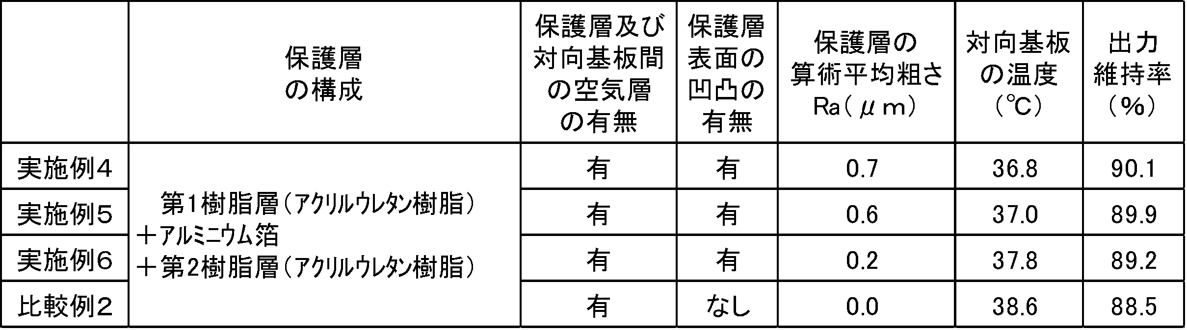
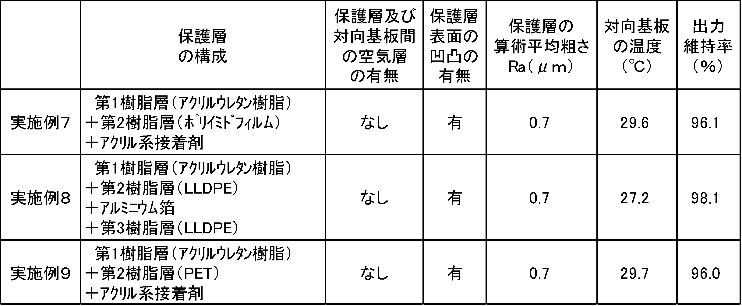
出力維持率は、実施例1~9および比較例1~2で得られた光電変換素子について、200ルクスの白色LEDを照射した状態で出力Wiを測定した。続いて、上記光電変換素子を55℃の恒温槽に受光面を下にした状態で24時間投入してから室温環境に移して受光面を下にした状態で30分間放置した後、200ルクスの白色LEDを照射した状態で出力Wfを測定した。そして、下記式により出力維持率(%)を算出した。結果を表1~3に示す。
出力維持率(%)=100×Wf/Wi
表1に示す結果より、実施例1~3の光電変換素子は、比較例1の光電変換素子に比べ、対向基板の温度が十分に低下し、出力維持率は増加することが分かった。
また表2に示す結果より、実施例4~6の光電変換素子は、比較例2の光電変換素子に比べ、対向基板の温度が十分に低下し、出力維持率は増加することが分かった。
さらに、表3に示す結果より、実施例7~9の光電変換素子でも、対向基板の温度が十分に低下し、出力維持率は増加することが分かった。
以上の結果より、本発明の光電変換素子によれば、周囲の温度が高温状態から低下する場合に、光電変換特性の回復性を向上させることができることが確認された。
11…透明基板
11b…セル設置面(一面)
12A…電極
20…光電変換セル
30…保護層
30a…保護層の透明基板と反対側の面
31…凹凸
50…対向基板
90…導電部材
100…光電変換素子
Y…透明基板の一面に直交する方向
11b…セル設置面(一面)
12A…電極
20…光電変換セル
30…保護層
30a…保護層の透明基板と反対側の面
31…凹凸
50…対向基板
90…導電部材
100…光電変換素子
Y…透明基板の一面に直交する方向
Claims (9)
- 透明基板と、
前記透明基板の一面上に設けられる少なくとも1つの光電変換セルと、
前記透明基板の前記一面側に設けられ、前記光電変換セルを覆って保護する保護層とを備える光電変換素子であって、
前記光電変換セルが、
前記透明基板の前記一面上に設けられる電極と、
前記電極に対向する対向基板とを備え、
前記光電変換素子を前記透明基板の前記一面に直交する方向に見た場合、前記保護層の前記透明基板と反対側の面のうち、少なくとも前記保護層と前記光電変換セルの前記対向基板とが重なり合う部分に凹凸が形成されている、光電変換素子。 - 前記保護層と前記対向基板とが密着している、請求項1に記載の光電変換素子。
- 前記保護層が樹脂層を有し、
前記樹脂層がポリイミド樹脂を含む、請求項1又は2に記載の光電変換素子。 - 前記対向基板が金属基板を有し、
前記保護層の前記樹脂層が前記対向基板の前記金属基板に密着している、請求項3に記載の光電変換素子。 - 前記金属基板に導電部材が接続されており、
前記保護層の前記樹脂層が前記導電部材にも密着している、請求項4に記載の光電変換素子。 - 前記凹凸が、算術平均粗さRaが0.2μm以上である凹凸である、請求項1~5のいずれか一項に記載の光電変換素子。
- 前記凹凸が、算術平均粗さRaが0.3μm以上である凹凸である、請求項6に記載の光電変換素子。
- 前記凹凸が、算術平均粗さRaが15μm以下である凹凸である、請求項1~7のいずれか一項に記載の光電変換素子。
- 前記保護層が黒色である、請求項1~8のいずれか一項に記載の光電変換素子。
Priority Applications (1)
| Application Number | Priority Date | Filing Date | Title |
|---|---|---|---|
| JP2018551628A JP6722769B2 (ja) | 2016-11-15 | 2017-11-13 | 光電変換素子 |
Applications Claiming Priority (2)
| Application Number | Priority Date | Filing Date | Title |
|---|---|---|---|
| JP2016222236 | 2016-11-15 | ||
| JP2016-222236 | 2016-11-15 |
Publications (1)
| Publication Number | Publication Date |
|---|---|
| WO2018092740A1 true WO2018092740A1 (ja) | 2018-05-24 |
Family
ID=62146579
Family Applications (1)
| Application Number | Title | Priority Date | Filing Date |
|---|---|---|---|
| PCT/JP2017/040824 Ceased WO2018092740A1 (ja) | 2016-11-15 | 2017-11-13 | 光電変換素子 |
Country Status (2)
| Country | Link |
|---|---|
| JP (1) | JP6722769B2 (ja) |
| WO (1) | WO2018092740A1 (ja) |
Citations (4)
| Publication number | Priority date | Publication date | Assignee | Title |
|---|---|---|---|---|
| JP2002260746A (ja) * | 2001-02-28 | 2002-09-13 | Toyota Central Res & Dev Lab Inc | 色素増感型太陽電池及び色素増感型太陽電池モジュール |
| JP2007317565A (ja) * | 2006-05-26 | 2007-12-06 | Stanley Electric Co Ltd | 有機光電変換素子 |
| JP2012018924A (ja) * | 2010-07-07 | 2012-01-26 | Toyota Motor Engineering & Manufacturing North America Inc | 回折格子を備えた太陽電池組立体 |
| JP2013207162A (ja) * | 2012-03-29 | 2013-10-07 | Nippon Zeon Co Ltd | 有機光電変換素子 |
-
2017
- 2017-11-13 WO PCT/JP2017/040824 patent/WO2018092740A1/ja not_active Ceased
- 2017-11-13 JP JP2018551628A patent/JP6722769B2/ja not_active Expired - Fee Related
Patent Citations (4)
| Publication number | Priority date | Publication date | Assignee | Title |
|---|---|---|---|---|
| JP2002260746A (ja) * | 2001-02-28 | 2002-09-13 | Toyota Central Res & Dev Lab Inc | 色素増感型太陽電池及び色素増感型太陽電池モジュール |
| JP2007317565A (ja) * | 2006-05-26 | 2007-12-06 | Stanley Electric Co Ltd | 有機光電変換素子 |
| JP2012018924A (ja) * | 2010-07-07 | 2012-01-26 | Toyota Motor Engineering & Manufacturing North America Inc | 回折格子を備えた太陽電池組立体 |
| JP2013207162A (ja) * | 2012-03-29 | 2013-10-07 | Nippon Zeon Co Ltd | 有機光電変換素子 |
Also Published As
| Publication number | Publication date |
|---|---|
| JPWO2018092740A1 (ja) | 2019-10-17 |
| JP6722769B2 (ja) | 2020-07-15 |
Similar Documents
| Publication | Publication Date | Title |
|---|---|---|
| AU2008258967B2 (en) | Dye-sensitized solar cell module and production method thereof | |
| CN102106032B (zh) | 光电转换元件模块、及光电转换元件模块的制造方法 | |
| EP2683020B1 (en) | Dye-sensitized solar cell module | |
| US20110226325A1 (en) | Photoelectric conversion device | |
| WO2009098857A1 (ja) | 色素増感太陽電池 | |
| JP6122156B2 (ja) | 光電変換素子 | |
| JP5451920B1 (ja) | 色素増感太陽電池素子 | |
| CN107924764B (zh) | 光电转换元件 | |
| JP6333343B2 (ja) | 光電変換素子 | |
| JP5465446B2 (ja) | 光電変換素子 | |
| JP5128118B2 (ja) | 湿式太陽電池とその製造方法 | |
| JP5680996B2 (ja) | 色素増感太陽電池モジュール及びその製造方法 | |
| JP6573497B2 (ja) | 光電変換素子 | |
| JP6722769B2 (ja) | 光電変換素子 | |
| JP2018081988A (ja) | 光電変換素子 | |
| JP2021044525A (ja) | 光電変換素子 | |
| EP3029695A1 (en) | Dye-sensitized solar cell element | |
| JP6694371B2 (ja) | 光電変換素子 | |
| JP6598757B2 (ja) | 光電変換素子 | |
| JP5095148B2 (ja) | 作用極用基板及び光電変換素子 | |
| JP5380619B1 (ja) | 色素増感太陽電池素子 | |
| JP6961532B2 (ja) | 光電変換素子 | |
| JP5945012B2 (ja) | 色素増感太陽電池素子 | |
| JP2021150345A (ja) | 光電変換素子及びその製造方法 | |
| JP2017034197A (ja) | 光電変換素子 |
Legal Events
| Date | Code | Title | Description |
|---|---|---|---|
| 121 | Ep: the epo has been informed by wipo that ep was designated in this application |
Ref document number: 17872101 Country of ref document: EP Kind code of ref document: A1 |
|
| ENP | Entry into the national phase |
Ref document number: 2018551628 Country of ref document: JP Kind code of ref document: A |
|
| NENP | Non-entry into the national phase |
Ref country code: DE |
|
| 122 | Ep: pct application non-entry in european phase |
Ref document number: 17872101 Country of ref document: EP Kind code of ref document: A1 |