WO2018092523A1 - 光電変換素子、固体撮像素子および電子装置 - Google Patents
光電変換素子、固体撮像素子および電子装置 Download PDFInfo
- Publication number
- WO2018092523A1 WO2018092523A1 PCT/JP2017/038245 JP2017038245W WO2018092523A1 WO 2018092523 A1 WO2018092523 A1 WO 2018092523A1 JP 2017038245 W JP2017038245 W JP 2017038245W WO 2018092523 A1 WO2018092523 A1 WO 2018092523A1
- Authority
- WO
- WIPO (PCT)
- Prior art keywords
- photoelectric conversion
- subphthalocyanine
- quinacridone
- conversion element
- solid
- Prior art date
- Legal status (The legal status is an assumption and is not a legal conclusion. Google has not performed a legal analysis and makes no representation as to the accuracy of the status listed.)
- Ceased
Links
Images









Classifications
-
- H—ELECTRICITY
- H10—SEMICONDUCTOR DEVICES; ELECTRIC SOLID-STATE DEVICES NOT OTHERWISE PROVIDED FOR
- H10F—INORGANIC SEMICONDUCTOR DEVICES SENSITIVE TO INFRARED RADIATION, LIGHT, ELECTROMAGNETIC RADIATION OF SHORTER WAVELENGTH OR CORPUSCULAR RADIATION
- H10F39/00—Integrated devices, or assemblies of multiple devices, comprising at least one element covered by group H10F30/00, e.g. radiation detectors comprising photodiode arrays
- H10F39/10—Integrated devices
- H10F39/12—Image sensors
- H10F39/191—Photoconductor image sensors
-
- H—ELECTRICITY
- H04—ELECTRIC COMMUNICATION TECHNIQUE
- H04N—PICTORIAL COMMUNICATION, e.g. TELEVISION
- H04N25/00—Circuitry of solid-state image sensors [SSIS]; Control thereof
- H04N25/70—SSIS architectures; Circuits associated therewith
- H04N25/71—Charge-coupled device [CCD] sensors; Charge-transfer registers specially adapted for CCD sensors
-
- H—ELECTRICITY
- H10—SEMICONDUCTOR DEVICES; ELECTRIC SOLID-STATE DEVICES NOT OTHERWISE PROVIDED FOR
- H10F—INORGANIC SEMICONDUCTOR DEVICES SENSITIVE TO INFRARED RADIATION, LIGHT, ELECTROMAGNETIC RADIATION OF SHORTER WAVELENGTH OR CORPUSCULAR RADIATION
- H10F39/00—Integrated devices, or assemblies of multiple devices, comprising at least one element covered by group H10F30/00, e.g. radiation detectors comprising photodiode arrays
- H10F39/10—Integrated devices
- H10F39/12—Image sensors
- H10F39/15—Charge-coupled device [CCD] image sensors
-
- H—ELECTRICITY
- H10—SEMICONDUCTOR DEVICES; ELECTRIC SOLID-STATE DEVICES NOT OTHERWISE PROVIDED FOR
- H10F—INORGANIC SEMICONDUCTOR DEVICES SENSITIVE TO INFRARED RADIATION, LIGHT, ELECTROMAGNETIC RADIATION OF SHORTER WAVELENGTH OR CORPUSCULAR RADIATION
- H10F39/00—Integrated devices, or assemblies of multiple devices, comprising at least one element covered by group H10F30/00, e.g. radiation detectors comprising photodiode arrays
- H10F39/10—Integrated devices
- H10F39/12—Image sensors
- H10F39/18—Complementary metal-oxide-semiconductor [CMOS] image sensors; Photodiode array image sensors
- H10F39/182—Colour image sensors
-
- H—ELECTRICITY
- H10—SEMICONDUCTOR DEVICES; ELECTRIC SOLID-STATE DEVICES NOT OTHERWISE PROVIDED FOR
- H10K—ORGANIC ELECTRIC SOLID-STATE DEVICES
- H10K30/00—Organic devices sensitive to infrared radiation, light, electromagnetic radiation of shorter wavelength or corpuscular radiation
- H10K30/20—Organic devices sensitive to infrared radiation, light, electromagnetic radiation of shorter wavelength or corpuscular radiation comprising organic-organic junctions, e.g. donor-acceptor junctions
-
- H—ELECTRICITY
- H10—SEMICONDUCTOR DEVICES; ELECTRIC SOLID-STATE DEVICES NOT OTHERWISE PROVIDED FOR
- H10K—ORGANIC ELECTRIC SOLID-STATE DEVICES
- H10K30/00—Organic devices sensitive to infrared radiation, light, electromagnetic radiation of shorter wavelength or corpuscular radiation
- H10K30/80—Constructional details
- H10K30/81—Electrodes
-
- H—ELECTRICITY
- H10—SEMICONDUCTOR DEVICES; ELECTRIC SOLID-STATE DEVICES NOT OTHERWISE PROVIDED FOR
- H10K—ORGANIC ELECTRIC SOLID-STATE DEVICES
- H10K39/00—Integrated devices, or assemblies of multiple devices, comprising at least one organic radiation-sensitive element covered by group H10K30/00
- H10K39/30—Devices controlled by radiation
- H10K39/32—Organic image sensors
-
- H—ELECTRICITY
- H10—SEMICONDUCTOR DEVICES; ELECTRIC SOLID-STATE DEVICES NOT OTHERWISE PROVIDED FOR
- H10K—ORGANIC ELECTRIC SOLID-STATE DEVICES
- H10K71/00—Manufacture or treatment specially adapted for the organic devices covered by this subclass
- H10K71/10—Deposition of organic active material
- H10K71/191—Deposition of organic active material characterised by provisions for the orientation or alignment of the layer to be deposited
-
- H—ELECTRICITY
- H10—SEMICONDUCTOR DEVICES; ELECTRIC SOLID-STATE DEVICES NOT OTHERWISE PROVIDED FOR
- H10K—ORGANIC ELECTRIC SOLID-STATE DEVICES
- H10K85/00—Organic materials used in the body or electrodes of devices covered by this subclass
- H10K85/60—Organic compounds having low molecular weight
- H10K85/649—Aromatic compounds comprising a hetero atom
- H10K85/657—Polycyclic condensed heteroaromatic hydrocarbons
- H10K85/6572—Polycyclic condensed heteroaromatic hydrocarbons comprising only nitrogen in the heteroaromatic polycondensed ring system, e.g. phenanthroline or carbazole
-
- H—ELECTRICITY
- H10—SEMICONDUCTOR DEVICES; ELECTRIC SOLID-STATE DEVICES NOT OTHERWISE PROVIDED FOR
- H10K—ORGANIC ELECTRIC SOLID-STATE DEVICES
- H10K30/00—Organic devices sensitive to infrared radiation, light, electromagnetic radiation of shorter wavelength or corpuscular radiation
- H10K30/451—Organic devices sensitive to infrared radiation, light, electromagnetic radiation of shorter wavelength or corpuscular radiation comprising a metal-semiconductor-metal [m-s-m] structure
-
- H—ELECTRICITY
- H10—SEMICONDUCTOR DEVICES; ELECTRIC SOLID-STATE DEVICES NOT OTHERWISE PROVIDED FOR
- H10K—ORGANIC ELECTRIC SOLID-STATE DEVICES
- H10K85/00—Organic materials used in the body or electrodes of devices covered by this subclass
- H10K85/30—Coordination compounds
- H10K85/311—Phthalocyanine
-
- Y—GENERAL TAGGING OF NEW TECHNOLOGICAL DEVELOPMENTS; GENERAL TAGGING OF CROSS-SECTIONAL TECHNOLOGIES SPANNING OVER SEVERAL SECTIONS OF THE IPC; TECHNICAL SUBJECTS COVERED BY FORMER USPC CROSS-REFERENCE ART COLLECTIONS [XRACs] AND DIGESTS
- Y02—TECHNOLOGIES OR APPLICATIONS FOR MITIGATION OR ADAPTATION AGAINST CLIMATE CHANGE
- Y02E—REDUCTION OF GREENHOUSE GAS [GHG] EMISSIONS, RELATED TO ENERGY GENERATION, TRANSMISSION OR DISTRIBUTION
- Y02E10/00—Energy generation through renewable energy sources
- Y02E10/50—Photovoltaic [PV] energy
- Y02E10/549—Organic PV cells
Definitions
- This technology relates to a photoelectric conversion element, a solid-state imaging element, and an electronic device.
- the photoelectric conversion element provided with the organic photoelectric converting layer containing organic materials, such as an organic molecule, a solid-state image sensor, and an electronic device.
- Patent Document 1 an organic photoelectric conversion film having sensitivity to blue light (B), an organic photoelectric conversion film having sensitivity to green light (G), and an organic photoelectric conversion film having sensitivity to red light (R).
- An image sensor using an organic photoelectric conversion film having a multilayer structure in which are sequentially stacked is disclosed. In this image sensor, sensitivity is improved by separately extracting B / G / R signals from one pixel.
- Patent Document 2 discloses an imaging device in which a single-layer organic photoelectric conversion film is formed, one color signal is extracted by the organic photoelectric conversion film, and two color signals are extracted by silicon (Si) bulk spectroscopy.
- Patent Document 3 discloses a solid-state imaging device including quinacridone or a derivative thereof in a photoelectric conversion film. Yes. Further, for example, Non-Patent Document 1 reports an image sensor having improved responsiveness by constituting a photoelectric conversion layer with dimethylquinacridone and subphthalocyanines.
- Patent Document 3 and Non-Patent Document 1 are insufficient as the responsiveness of the photoelectric conversion element, and may not improve the external quantum efficiency.
- the present technology has been made in view of such a situation, and a main object is to provide a photoelectric conversion element with improved responsiveness and external quantum efficiency.
- the present inventors have improved responsiveness and external quantum efficiency by adjusting the molecular orientation of organic molecules contained in the organic photoelectric conversion layer. Successful, this technology was completed.
- an organic photoelectric conversion layer sandwiched between a first electrode and a second electrode is provided, and the organic photoelectric conversion layer includes organic molecules of a quinacridone (QD) derivative and a subphthalocyanine (SubPc) derivative.
- QD quinacridone
- SubPc subphthalocyanine
- a photoelectric conversion element in which at least a quinacridone derivative of organic molecules is randomly oriented.
- the present technology provides a solid-state imaging device in which at least a photoelectric conversion device according to the present technology and a semiconductor substrate are stacked for each of a plurality of pixels arranged one-dimensionally or two-dimensionally.
- the present technology provides an electronic device including the solid-state imaging device according to the present technology.
- the present technology it is possible to provide a photoelectric conversion element with improved responsiveness and external quantum efficiency.
- the effect described here is not necessarily limited, and may be any effect described in the present technology.
- First embodiment organic photoelectric conversion element 1-1.
- Surface irradiation type solid-state imaging device Third Embodiment (Electronic Device) 4).
- Application example to endoscopic surgery system Application examples for moving objects
- FIG. 1 is a cross-sectional view illustrating a configuration example of the organic photoelectric conversion element 10 according to the first embodiment of the present technology.
- the organic photoelectric conversion element 10 includes, from a lower layer to an upper layer, a first electrode (lower electrode) 11, a first buffer layer 12, an organic photoelectric conversion layer 13, a second buffer layer 14, A second electrode (upper electrode) 15 is stacked in this order.
- the organic photoelectric conversion layer 13 contains one or more quinacridone (QD) derivatives and one or more subphthalocyanine (SubPc) derivatives.
- QD quinacridone
- SubPc subphthalocyanine
- the average inclination of the molecules is randomly oriented.
- random orientation means that the angle ⁇ formed by the average orientation of the transition dipole moment of molecules and the normal n of the laminated surface with respect to the surface of the organic photoelectric conversion layer 13 is 50 ° to 60 °.
- Examples of the quinacridone derivative applicable to the organic photoelectric conversion layer 13 include 2,9-diethylquinacridone (EQD), 2,9-di-tert-butylquinacridone (BQD), and N, N′-dimethyl.
- the subphthalocyanine derivative in the organic photoelectric conversion layer 13 exists in an amorphous state, but part or all of the subphthalocyanine derivative also has a random average molecular inclination.
- Examples of the types of subphthalocyanine derivatives applicable to the organic photoelectric conversion layer 13 include boron subphthalocyanine chloride (SubPc-Cl), boron subphthalocyanine-4-chlorophenoxide (SubPc-OPhCl), hexafluoroboron subphthalocyanine chloride ( F6-SubPc-Cl), hexafluoroboron subphthalocyanine-4-chlorophenoxide (F6-SubPc-OPhCl), boron subphthalocyanine fluoride (SubPc-F), boron subphthalocyanine-4-pyridinoxide (SubPc-Opy), boron Examples include, but are not limited to, subphthalocyanine-4-fluorophenoxide (SubPc-OphF), pentafluoroboron subphthalocyanine (SubPc-OC6F5), dodecafluoroboron subphthalocyanine chloride (F12-SubPc-Cl),
- the organic photoelectric conversion layer 13 shows an example in which one kind of quinacridone derivative and one subphthalocyanine derivative is included.
- the present invention is not limited to this, and two or more kinds of quinacridone derivatives or subphthalocyanine derivatives are contained. May be.
- the first electrode 11 and the second electrode 15 are made of, for example, a light transmissive transparent conductive material, specifically, ITO (Indium-Tin-Oxide).
- the first electrode 11 may be made of a tin oxide (SnO 2 ) -based material or a zinc oxide (ZnO) -based material.
- the tin oxide-based material is a tin oxide added with a dopant
- the zinc oxide-based material is, for example, aluminum zinc oxide (AZO) obtained by adding aluminum (Al) as a dopant to zinc oxide, and zinc oxide as a dopant.
- AZO aluminum zinc oxide
- Examples thereof include gallium zinc oxide (GZO) to which gallium (Ga) is added, indium zinc oxide (IZO) to which zinc oxide is added with indium (In) as a dopant.
- GZO gallium zinc oxide
- IZO indium zinc oxide
- IGZO, CuI, InSbO 4 , ZnMgO, CuInO 2 , MgIn 2 O 4 , CdO, ZnSnO 3, and the like can be used.
- the thicknesses of the first electrode 11 and the second electrode 15 may be arbitrary, but are, for example, 50 nm to 500 nm, respectively.
- the first electrode 11 is formed.
- the first electrode 11 is formed by, for example, forming an ITO film by a sputtering method, patterning the ITO film by a photolithography technique, and performing dry etching or wet etching.
- the first buffer layer 12 is formed on the first electrode 11.
- a coating method including a casting method and a spin coating method
- An organic photoelectric conversion layer 13 is formed on the first buffer layer 12.
- a second buffer layer 14 is formed on the photoelectric conversion layer 13.
- a coating method including a casting method and a spin coating method
- the second electrode 15 is formed on the second buffer layer 14 by vacuum deposition or the like, and the organic photoelectric conversion element 10 is manufactured.
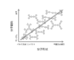
- FIG. 2 is a graph showing the general relationship between the molecular shape and molecular orientation of organic molecules (Source: J. Mater. Chem., 2011, 21, 19187, Fig. 7).
- FIG. 3 is a schematic diagram showing the orientation of the quinacridone derivative constituting the organic photoelectric conversion element 10 of the present embodiment.
- FIG. 3A shows a cross section of the quinacridone derivative
- FIG. 3B shows the quinacridone derivative viewed from the normal direction of the film surface. The orientation of the quinacridone derivative will be described with reference to FIGS.
- the quinacridone derivative is oriented such that the long axis direction of the quinacridone 20 is aligned in the horizontal direction.
- the quinacridone 20 is oriented in the horizontal direction, particularly when the film is formed at a low temperature, depending on the film forming conditions.
- quinacridone 20 is randomly oriented in the film plane.
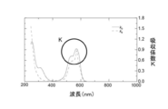
- FIG. 4 is a graph showing the absorption coefficient K obtained from the result of measurement using spectroscopic ellipsometry and fitting using an anisotropic model.
- the solid line graph in FIG. 4 represents the horizontal direction Ko of the absorption coefficient K
- the dotted line graph represents the vertical direction Ke of the absorption coefficient K.
- the circle at the center of FIG. 4 represents the position of the maximum value of the absorption coefficient K.
- the method for obtaining the orientation parameter S will be described with reference to FIG.
- the orientation parameter S is the maximum vertical (Ke) and horizontal (K0) values of the optical constant (absorption coefficient) K obtained by analysis using an anisotropic model based on the spectroscopic ellipsometry measurement results. Can be used to calculate.
- the orientation parameter S the degree of molecular orientation can be determined.
- the orientation parameter S of the quinacridone derivative can be obtained by the following equation (1).
- the measurement method by the above spectroscopic ellipsometry is a known technique, and the present technique is not limited to the above technique, and for example, a known polarization Raman spectroscopy can be used.
- FIG. 5 is a schematic diagram for explaining orientation parameters of particles having shape anisotropy.
- FIG. 5B shows the shape anisotropy.
- the shape anisotropic particles 41 are oriented in the normal n direction or the direction of one plane, the shape anisotropic particles 41 in such an orientation state are included.
- the photoelectric conversion element provided with the photoelectric conversion layer has insufficient responsiveness. This is probably because when the molecules are oriented, there is a time difference between the movement of electrons and holes depending on the direction of the molecules.
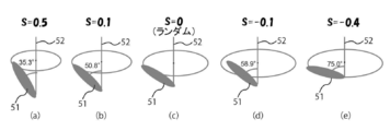
- FIG. 6 is a graph showing the relationship between the orientation parameter S and the average slope of the distribution of quinacridone 51.
- the average slope of the distribution of quinacridone 51 is ⁇ n i cos 2 ⁇ i, where n i is the number of molecules of quinacridone 51 in the organic photoelectric conversion layer 13 and ⁇ i is the slope of the i-th quinacridone 51. Can be sought.
- FIG. 7 is a flowchart showing a method for deriving a crystal grain size by X-ray diffraction (XRD). An example of a method for deriving the crystal grain size of the quinacridone derivative will be described with reference to FIG.
- step S701 XRD measurement is started using an X-ray diffractometer aligned (adjusted) in the parallel method (thin film method).
- the incident angle of X-rays is fixed to 1 ° or less with respect to the sample surface, and the detector angle 2 ⁇ is measured in the range of 3 ° to 35 °.
- step S702 the full width at half maximum (FWHM) B exp is obtained by peak separation using a known Peason VII or pseudo-Forked function.
- step S703 the measurement of commercially available standard samples or grain size 100 nm, finding a B i (spread correction of X-ray) device factor correction.
- the X-ray spread correction B i can be obtained using the following equation (2).
- ⁇ (Bexp 2 ⁇ Bi 2 ) 1/2 (2)
- beta is the spread of diffraction line by crystallite (rad)
- the B i is spread (rad)
- the diffraction line by the device the diffraction line by the device.
- the particle size Dnm can be derived by the following Scherrer equation (3).
- D K ⁇ / ⁇ cos ⁇ (3)
- K is the Scherrer constant of 0.94
- ⁇ is the X-ray wavelength (nm)
- ⁇ is the diffraction line spread (rad)
- ⁇ is the diffraction angle (rad).
- the particle size Dnm is derived by the above method, but the deriving method is not limited to this, and any method may be used as long as the particle size Dnm is obtained.
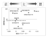
- FIG. 8 is a diagram showing the relationship between the orientation parameter S and the responsiveness according to the type of organic molecules in the case of random orientation. The value of the orientation parameter S that provides good responsiveness will be described with reference to FIG.
- the horizontal axis represents the orientation parameter S
- the vertical axis represents the response (msec).
- the orientation parameter S is 0, the orientation is random, and as the orientation parameter S becomes smaller than 0, the orientation becomes horizontal, and as the orientation parameter S becomes larger than 0, the orientation becomes vertical.
- the responsiveness indicates that the smaller the numerical value, the better. That is, the larger the value, the faster the afterimage disappears and does not remain.
- ⁇ represents a binary system (including two types of organic molecules), and ⁇ represents a ternary system (including three types of organic molecules).
- the responsiveness shows a good value of 100 (msec) or less.
- BQD: F6 which is a binary system has a response of 10.0 (msec)
- QD: BQD: F6 which is a ternary system has a response. Is 7.5 (msec), indicating a very good value.
- FIG. 9 is a diagram showing the relationship between crystal grain size and responsiveness according to the type of organic molecules in the case of random orientation. With reference to FIG. 9, the size of the crystal grain size at which the responsiveness is good will be described.
- the horizontal axis indicates the crystal grain size (nm), and the vertical axis indicates the response (msec).
- ⁇ in FIG. 9 represents a binary system, and ⁇ represents a ternary system.
- the responsiveness becomes better as the crystal grain size goes from both around 1 nm and around 6.5 nm to around 2 to 3 nm.
- the responsiveness shows a good value of 10 (msec) or less.
- the responsiveness of ternary MMQD: BQD: F6 shows a peak of about 2 to 3 (msec).
- the responsiveness of the organic photoelectric conversion element 10 of this embodiment can be improved.
- the quinacridone derivative and the subphthalocyanine derivative are randomly oriented and the crystal grain size of the quinacridone derivative and the subphthalocyanine derivative is about 2 to 5 nm
- the responsiveness of the organic photoelectric conversion element 10 can be improved. it can.
- by reducing the particle size of the quinacridone derivative (5 nm or less) defects in the interface trap and the organic photoelectric conversion layer can be reduced.
- the charge mobility is greatly reduced by the grain boundary (grain boundary) generated in the polycrystalline organic photoelectric conversion layer 13. This is because in the grain boundary, an electron trap and a hole barrier are formed, and the overlap of atomic orbitals is reduced, thereby making it difficult for charges to move. Therefore, in order to improve the charge mobility (carrier mobility), it is important to create a uniform structure in which no grain boundary is formed.
- the molecular orientation of the organic molecules in the organic photoelectric conversion layer 13 becomes strong, the ⁇ orbitals tend to overlap, but the crystals tend to be formed, and a grain boundary is likely to be formed. A boundary is formed.
- the photoelectric conversion element according to the first embodiment of the present technology was manufactured as follows, and the photoelectric conversion efficiency (external quantum efficiency), the responsiveness, and the crystal grain size of the quinacridone derivative were evaluated.
- Example 1 First, the glass substrate with an ITO electrode was washed by UV / ozone treatment.
- the film thickness of the ITO film corresponding to the lower electrode (first electrode) in the glass substrate was 50 nm.
- the glass substrate is put into an organic vapor deposition apparatus, the pressure is reduced to 1 ⁇ 10 ⁇ 5 Pa or less, and N-methyl-2,9-di-tert-butylquinacridone (BMQD) is rotated while rotating the substrate holder.
- BQD 2,9-di-tert-butylquinacridone
- F6-SubPc-Cl hexafluoroboron subphthalocyanine chloride
- AlSiCu was formed into a film with a film thickness of 100 nm on the organic photoelectric conversion layer by a vapor deposition method to form an upper electrode (second electrode).
- a photoelectric conversion element having a 1 mm ⁇ 1 mm photoelectric conversion region was manufactured by the above manufacturing method.
- Example 2 instead of N-methyl-2,9-di-tert-butylquinacridone (BMQD) in Example 1, N-methyl-2,9-dimethylquinacridone (TMQD; Example 2) Hexa in place of N-methylquinacridone (MMQD; Example 3), N-phenylquinacridone (MPQD; Example 4), TMQD and hexafluoroboron subphthalocyanine chloride (F6-SubPc-Cl) in Example 1 Quinacridone instead of fluoroboron subphthalocyanine-4-chlorophenoxide (F6-SubPc-OPh; Example 5), N-methylquinacridone (MMQD) and 2,9-di-tert-butylquinacridone (BQD) of Example 1 (QD; Example 6) was used to produce a photoelectric conversion element using the same method as in Example 1 (see Table 1). Table 1 shows the evaluation results of external quantum efficiency (EQE), responsiveness,
- the external photoelectric conversion efficiency evaluation method was evaluated using a semiconductor parameter analyzer. Specifically, the light current value when the amount of light irradiated from the light source to the photoelectric conversion element through the filter is 1.62 ⁇ W / cm 2 and the bias voltage applied between the electrodes is ⁇ 1 V, and The external photoelectric conversion efficiency was calculated from the dark current value.
- the optical anisotropy was measured using an anisotropy model with a spectroscopic ellipsometer, and the orientation parameter S was calculated from the absorption peak at 500 nm to 600 nm.
- Regarding the orientation direction since optical absorption is detected, it means the orientation in the direction of the transition dipole moment of each molecule, not necessarily the long axis direction of the molecule.
- the spectroscopic ellipsometer was measured at 5 ° intervals of 55 ° to 75 ° in a wavelength range of 245 nm to 1000 nm using Woolum M2000.
- a spectroscopic ellipso sample preparation method can form a 50 nm film on a 1-inch quartz substrate by a vacuum deposition method at a film formation rate of 1 ⁇ / sec.
- the correction of the apparatus coefficient was performed by correcting the X-ray divergence using the full width at half maximum of the Si particle having a sufficiently large particle diameter. As a result, the average half width of the Si particle peak was 0.73 ° (B i ). Then, the device coefficient was corrected using the formula (Bexp 2 ⁇ B i 2 ) 1/2 .
- Example 2 a photoelectric conversion element (Examples 7 to 9) was produced using the same method as in Example 1 except for the configuration of the organic photoelectric conversion layer, and its external quantum efficiency (EQE), responsiveness, and quinacridone derivative The crystal grain size of was evaluated as follows.
- N N′-diphenylquinacridone (DPQD; Example 7), N, N instead of N-methyl-2,9-di-tert-butylquinacridone (BMQD) of Example 1
- BQD 2,9-diphenyl-2,9-di-tert-butylquinacridone
- BQD 2,9-di-tert-butylquinacridone
- a photoelectric conversion device was produced in the same manner as in Example 1 except that quinacridone was used in all of Examples 7 to 9 instead of di-tert-butylquinacridone (BQD) (see Table 2).
- Table 2 shows the evaluation results of Examples 7 to 9 using two types of quinacridone derivatives other than the HR + HH type structure. Note that the evaluation results of EQE and responsiveness are expressed as relative values with the result of Example 1 as the reference value 1.
- Example 3 a photoelectric conversion element (Examples 10 to 11) was produced using the same method as in Example 1 except for the configuration of the organic photoelectric conversion layer, and its external quantum efficiency (EQE), responsiveness, and quinacridone derivative The crystal grain size of was evaluated as follows. However, the film formation rates in Experiment 3 are 0.05 nm / second and 0.05 nm / second.
- Example 10 instead of N-methyl-2,9-di-tert-butylquinacridone (BMQD) of Example 1, N-methylquinacridone (MMQD) (Example 10), N, N′- Dimethylquinacridone (DMQD) (Example 11) was used, and 2,9-di-tert-butylquinacridone (BQD) of Example 1 was not used in all of Examples 10 to 11, and the same as in Example 1.
- the photoelectric conversion element was produced using the method (see Table 3). Table 3 shows the evaluation results of Examples 10 to 11 using one kind of quinacridone derivative other than the HR + HH type structure. Note that the evaluation results of EQE and responsiveness are expressed as relative values with the result of Example 1 as the reference value 1.
- Example 4 As Comparative Examples 1 to 4, as quinacridone derivatives, only quinacridone was used in Comparative Examples 1 to 3, and 2,9-dimethylquinacridone (PR122) and 2,9-di-tert-butylquinacridone (BQD) were used in Comparative Example 4. It was. Further, the subphthalocyanine derivative is boron subphthalocyanine chloride (SubPc-Cl) in Comparative Example 1, hexafluoroboron subphthalocyanine-4-chlorophenoxide (SubPc-OPh) in Comparative Example 2, and hexafluorocarbon in Comparative Examples 3 and 4. Fluoroboron subphthalocyanine chloride (F6-SubPc-Cl) was used.
- SubPc-Cl boron subphthalocyanine chloride
- SubPc-OPh hexafluoroboron subphthalocyanine-4-chlorophenoxide
- F6-SubPc-Cl Fluoroboron subphthal
- Example 4 shows the evaluation results of Comparative Examples 1 to 4 in which the crystal grain size or the orientation parameter S is too large and the response is poor. Note that the evaluation results of EQE and responsiveness are expressed as relative values with the result of Example 1 as the reference value 1.
- the quinacridone derivative was 2,9-di-tert-butylquinacridone (BQD) only in Comparative Example 5, and N, N′-dimethylquinacridone (DMQD) and 2,9- Di-tert-butylquinacridone (BQD), N, N′-diphenylquinacridone (DPQD) and 2,9-di-tert-butylquinacridone (BQD) in Comparative Example 7, and 2,9-diethyl in Comparative Example 8 Quinacridone (EQD) and 2,9-di-tert-butylquinacridone (BQD) were used.
- BQD 2,9-di-tert-butylquinacridone
- hexafluoroboron subphthalocyanine chloride F6-SubPc-Cl
- the photoelectric conversion element was produced using the method similar to Example 1 (refer Table 5).
- Table 5 shows the evaluation results of Comparative Examples 5 to 8 in which the crystal grain size is too small and the response is poor. Note that the evaluation results of EQE and responsiveness are expressed as relative values with the result of Example 1 as the reference value 1.
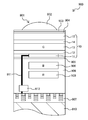
- FIG. 10 is a cross-sectional view illustrating a configuration example of a solid-state image sensor according to a second embodiment to which the present technology is applied.
- a solid-state imaging device 900 according to this embodiment will be described with reference to FIG.
- FIG. 10 shows, as an example, one pixel 901 among a plurality of pixels included in a back-illuminated solid-state imaging device 900 such as a CMOS image sensor.
- the pixel 901 includes an on-chip lens (OCL) 902, a planarization layer 903, a protective layer 904, the organic photoelectric conversion element 10, an insulating film 905, and a semiconductor in the depth direction from the light receiving surface of the solid-state imaging device 900.
- a substrate (silicon substrate) 906 and a multilayer wiring layer 907 are provided.
- a first photodiode 908 and a second photodiode 909 which are two inorganic photoelectric conversion units having a pn junction are formed in the semiconductor substrate 906.
- a support substrate 910 made of silicon, for example, is bonded to the multilayer wiring layer 907.
- the semiconductor substrate 906 On the back side of the semiconductor substrate 906 (upper side of the semiconductor substrate 906 in FIG. 10), a light receiving surface on which light is incident is formed, and on the front side of the semiconductor substrate 906 (lower side of the semiconductor substrate 906 in FIG. 10). A circuit including a readout circuit and the like is formed. That is, the pixel 901 has a light receiving surface on the back surface side of the semiconductor substrate 906 and a circuit formation surface on the front surface side of the semiconductor substrate 906.
- the semiconductor substrate 906 may be composed of either a p-type or an n-type semiconductor, where the first conductivity type is p-type and the second conductivity type is n-type.
- the first photodiode 908 is formed first from the back side of the semiconductor substrate 906 in the depth direction (downward direction in FIG. 10), and then the second photodiode 909 is formed. Is formed. In FIG. 10, the first photodiode 908 is for blue (B), and the second photodiode 909 is for red (R).
- a first electrode (lower electrode) 11, a first buffer layer 12, an organic photoelectric conversion layer 13, and a second buffer layer 14 are disposed on the back surface of the semiconductor substrate 906 on which the first photodiode 908 and the second photodiode 909 are formed.
- the organic photoelectric conversion element 10 in which the second electrode (upper electrode) 15 is stacked in this order is disposed.
- the organic photoelectric conversion device 10 is for green (G).
- the first electrode 11 and the second electrode in the organic photoelectric conversion element 10 may be formed of a transparent conductive film such as an indium tin oxide film or an indium zinc oxide film, for example.
- the organic photoelectric conversion layer 13 is a light absorption layer for photoelectrically converting incident light, and is generally crystalline silicon (Si) at visible wavelengths.
- the organic photoelectric conversion element 10 is green, the first photodiode 908 is blue, and the second photodiode 909 is red as color combinations.
- the organic photoelectric conversion element 10 can be red or blue, and the first photodiode 908 and the second photodiode 909 can be set to other corresponding colors. In this case, the position in the depth direction of the first photodiode 908 and the second photodiode 909 is set according to the color.
- the organic photoelectric conversion element 10UV for ultraviolet light and / or the organic for infrared light may be applied to the solid-state imaging device (backside irradiation type solid-state imaging device and front-side irradiation type solid-state imaging device) according to the second embodiment of the present technology.
- the organic photoelectric conversion element 10UV for ultraviolet light and / or the organic photoelectric conversion element 10IR for infrared light it becomes possible to detect light having a wavelength other than the visible light region.
- a wiring 911 connected to the first electrode 11 and a wiring (not shown) connected to the second electrode 15 are formed.
- Examples of the wiring connected to the wiring 911 and the second electrode 15 include a tungsten (W) plug having a SiO 2 or SiN insulating layer in the periphery in order to suppress a short circuit with Si, a semiconductor layer by ion implantation, or the like. Can be formed.
- the wiring 911 is a p-type semiconductor layer when formed of a semiconductor layer by ion implantation.
- the wiring connected to the second electrode 15 can use an n-type semiconductor layer because the second electrode 15 extracts electrons.
- an n-type region 912 for accumulating charges is formed on the surface side in the semiconductor substrate 906.
- the n-type region 910 functions as a floating diffusion portion of the organic photoelectric conversion element 10.
- a film having a negative fixed charge can be used as the insulating film 905 on the back surface of the semiconductor substrate 906 .
- a film having a negative fixed charge for example, a hafnium oxide film can be used. That is, the insulating film 905 may be formed to have a three-layer structure in which a silicon oxide film, a hafnium oxide film, and a silicon oxide film are sequentially formed from the back surface side of the semiconductor substrate 906.
- the element 10 ⁇ / b> R may be applied to the solid-state imaging device (back-illuminated solid-state imaging device and front-illuminated solid-state imaging device) of the second embodiment according to the present technology.
- an organic photoelectric conversion material containing a phthalocyanine-based dye can be used as the organic photoelectric conversion element 10R that performs photoelectric conversion with red wavelength light.
- organic photoelectric conversion element 10G that performs photoelectric conversion with green wavelength light
- organic photoelectric conversion material containing a rhodamine dye, a melocyanine dye, quinacridone, or the like can be used.
- organic photoelectric conversion element 10B that performs photoelectric conversion with blue wavelength light
- an organic photoelectric conversion material containing a coumarin dye, tris-8-hydroxyquinoline Al (Alq3), a melocyanine dye, or the like can be used.
- the solid-state image sensor according to the second embodiment of the present technology can be applied not only to the above-described back-illuminated solid-state image sensor 900 but also to a front-illuminated solid-state image sensor.
- the back-illuminated solid-state image sensor 900 in which the multilayer wiring layer 910 is formed below the semiconductor substrate 906 is arranged between the organic photoelectric conversion element 10 and the semiconductor substrate 906. The only difference is that the multilayer wiring layer 910 is formed. Since the configuration of the other front-illuminated solid-state image sensor is the same as that of the back-illuminated solid-state image sensor 900, the description thereof is omitted here.
- the electronic apparatus includes the solid-state imaging device according to the second embodiment of the present technology, and the solid-state imaging device is at least for each of a plurality of pixels arranged one-dimensionally or two-dimensionally.
- 1 is an electronic device in which the photoelectric conversion element of the first embodiment according to the present technology and a semiconductor substrate are stacked. Since the electronic device according to the third embodiment of the present technology includes the solid-state imaging device with improved responsiveness and external quantum efficiency, it is possible to improve performance such as image quality of a color image.
- FIG. 11 is a diagram illustrating a usage example of the solid-state imaging device according to the second embodiment of the present technology as an image sensor.
- the solid-state imaging device of the second embodiment described above can be used in various cases for sensing light such as visible light, infrared light, ultraviolet light, and X-rays as follows. That is, as shown in FIG. 11, for example, the field of appreciation for taking images for appreciation, the field of transportation, the field of consumer electronics, the field of medical / healthcare, the field of security, the field of beauty, sports
- the solid-state imaging device according to the second embodiment can be used for devices (for example, the electronic device according to the third embodiment described above) used in the fields of No. 1 and agriculture.
- the solid-state imaging according to the second embodiment is applied to an apparatus for shooting an image provided for viewing, such as a digital camera, a smartphone, or a mobile phone with a camera function.
- An element can be used.
- in-vehicle sensors that capture images of the front, rear, surroundings, and interior of a vehicle for safe driving such as automatic stop and recognition of the driver's condition, traveling vehicles and roads are monitored.
- the solid-state image sensor according to the second embodiment can be used in a device used for traffic, such as a surveillance camera that performs a distance measurement between vehicles, a distance measurement sensor that performs distance measurement between vehicles, and the like.
- a solid-state image sensor in the form can be used.
- the solid-state imaging according to the second embodiment is applied to a device used for medical treatment or health care such as an endoscope or a blood vessel photographing device that receives infrared light.
- a device used for medical treatment or health care such as an endoscope or a blood vessel photographing device that receives infrared light.
- An element can be used.
- the solid-state image sensor according to the second embodiment can be used in devices used for security, such as surveillance cameras for crime prevention and cameras for personal authentication.
- the solid-state image sensor according to the second embodiment can be used in a device used for beauty, such as a skin measuring device that photographs skin and a microscope that photographs the scalp. .
- the solid-state image sensor according to the second embodiment can be used in devices used for sports such as action cameras and wearable cameras for sports applications.
- the solid-state imaging device of the second embodiment can be used in an apparatus used for agriculture, such as a camera for monitoring the state of fields and crops.
- the technology (this technology) according to the present disclosure can be applied to various products.
- an application example to an endoscopic surgery system and an application example to a moving body will be described.
- FIG. 12 is a diagram illustrating an example of a schematic configuration of an endoscopic surgery system to which the technology (present technology) according to the present disclosure can be applied.
- FIG. 12 shows a state in which an operator (doctor) 11131 is performing surgery on a patient 11132 on a patient bed 11133 using an endoscopic surgery system 11000.
- an endoscopic surgery system 11000 includes an endoscope 11100, other surgical instruments 11110 such as an insufflation tube 11111 and an energy treatment instrument 11112, and a support arm device 11120 that supports the endoscope 11100. And a cart 11200 on which various devices for endoscopic surgery are mounted.
- the endoscope 11100 includes a lens barrel 11101 in which a region having a predetermined length from the distal end is inserted into the body cavity of the patient 11132, and a camera head 11102 connected to the proximal end of the lens barrel 11101.
- a lens barrel 11101 in which a region having a predetermined length from the distal end is inserted into the body cavity of the patient 11132, and a camera head 11102 connected to the proximal end of the lens barrel 11101.
- an endoscope 11100 configured as a so-called rigid mirror having a rigid lens barrel 11101 is illustrated, but the endoscope 11100 may be configured as a so-called flexible mirror having a flexible lens barrel. Good.
- An opening into which the objective lens is fitted is provided at the tip of the lens barrel 11101.
- a light source device 11203 is connected to the endoscope 11100, and light generated by the light source device 11203 is guided to the tip of the lens barrel by a light guide extending inside the lens barrel 11101. Irradiation is performed toward the observation target in the body cavity of the patient 11132 through the lens.
- the endoscope 11100 may be a direct endoscope, a perspective mirror, or a side endoscope.
- An optical system and an image sensor are provided inside the camera head 11102, and reflected light (observation light) from the observation target is condensed on the image sensor by the optical system. Observation light is photoelectrically converted by the imaging element, and an electrical signal corresponding to the observation light, that is, an image signal corresponding to the observation image is generated.
- the image signal is transmitted to a camera control unit (CCU: Camera Control Unit) 11201 as RAW data.
- CCU Camera Control Unit
- the CCU 11201 is configured by a CPU (Central Processing Unit), a GPU (Graphics Processing Unit), and the like, and comprehensively controls operations of the endoscope 11100 and the display device 11202. Further, the CCU 11201 receives an image signal from the camera head 11102 and performs various kinds of image processing for displaying an image based on the image signal, such as development processing (demosaic processing), for example.
- a CPU Central Processing Unit
- GPU Graphics Processing Unit
- the display device 11202 displays an image based on an image signal subjected to image processing by the CCU 11201 under the control of the CCU 11201.
- the light source device 11203 is composed of a light source such as an LED (Light Emitting Diode), for example, and supplies irradiation light to the endoscope 11100 when photographing a surgical site or the like.
- a light source such as an LED (Light Emitting Diode), for example, and supplies irradiation light to the endoscope 11100 when photographing a surgical site or the like.
- the input device 11204 is an input interface for the endoscopic surgery system 11000.
- a user can input various information and instructions to the endoscopic surgery system 11000 via the input device 11204.
- the user inputs an instruction to change the imaging conditions (type of irradiation light, magnification, focal length, etc.) by the endoscope 11100.
- the treatment instrument control device 11205 controls the drive of the energy treatment instrument 11112 for tissue ablation, incision, blood vessel sealing, or the like.
- the pneumoperitoneum device 11206 passes gas into the body cavity via the pneumoperitoneum tube 11111.
- the recorder 11207 is an apparatus capable of recording various types of information related to surgery.
- the printer 11208 is a device that can print various types of information related to surgery in various formats such as text, images, or graphs.
- the light source device 11203 that supplies the irradiation light when the surgical site is imaged to the endoscope 11100 can be configured by, for example, a white light source configured by an LED, a laser light source, or a combination thereof.
- a white light source is configured by a combination of RGB laser light sources, the output intensity and output timing of each color (each wavelength) can be controlled with high accuracy. Therefore, the light source device 11203 adjusts the white balance of the captured image. It can be carried out.
- the driving of the light source device 11203 may be controlled so as to change the intensity of the output light every predetermined time. Synchronously with the timing of changing the intensity of the light, the drive of the image sensor of the camera head 11102 is controlled to acquire an image in a time-sharing manner, and the image is synthesized, so that high dynamic without so-called blackout and overexposure A range image can be generated.
- the light source device 11203 may be configured to be able to supply light of a predetermined wavelength band corresponding to special light observation.
- special light observation for example, by utilizing the wavelength dependence of light absorption in body tissue, the surface of the mucous membrane is irradiated by irradiating light in a narrow band compared to irradiation light (ie, white light) during normal observation.
- a so-called narrow band imaging is performed in which a predetermined tissue such as a blood vessel is imaged with high contrast.
- fluorescence observation may be performed in which an image is obtained by fluorescence generated by irradiating excitation light.
- the body tissue is irradiated with excitation light to observe fluorescence from the body tissue (autofluorescence observation), or a reagent such as indocyanine green (ICG) is locally administered to the body tissue and applied to the body tissue. It is possible to obtain a fluorescence image by irradiating excitation light corresponding to the fluorescence wavelength of the reagent.
- the light source device 11203 can be configured to be able to supply narrowband light and / or excitation light corresponding to such special light observation.
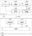
- FIG. 13 is a block diagram showing an example of the functional configuration of the camera head 11102 and CCU 11201 shown in FIG.
- the camera head 11102 includes a lens unit 11401, an imaging unit 11402, a drive unit 11403, a communication unit 11404, and a camera head control unit 11405.
- the CCU 11201 includes a communication unit 11411, an image processing unit 11412, and a control unit 11413.
- the camera head 11102 and the CCU 11201 are connected to each other by a transmission cable 11400 so that they can communicate with each other.
- the lens unit 11401 is an optical system provided at a connection portion with the lens barrel 11101. Observation light taken from the tip of the lens barrel 11101 is guided to the camera head 11102 and enters the lens unit 11401.
- the lens unit 11401 is configured by combining a plurality of lenses including a zoom lens and a focus lens.
- the imaging unit 11402 includes an imaging element.
- One (so-called single plate type) image sensor may be included in the imaging unit 11402, or a plurality (so-called multi-plate type) may be used.
- image signals corresponding to RGB may be generated by each imaging element, and a color image may be obtained by combining them.
- the imaging unit 11402 may be configured to include a pair of imaging elements for acquiring right-eye and left-eye image signals corresponding to 3D (Dimensional) display. By performing the 3D display, the operator 11131 can more accurately grasp the depth of the living tissue in the surgical site.
- 3D 3D
- the imaging unit 11402 is not necessarily provided in the camera head 11102.
- the imaging unit 11402 may be provided inside the lens barrel 11101 immediately after the objective lens.
- the driving unit 11403 is configured by an actuator, and moves the zoom lens and the focus lens of the lens unit 11401 by a predetermined distance along the optical axis under the control of the camera head control unit 11405. Thereby, the magnification and the focus of the image captured by the imaging unit 11402 can be adjusted as appropriate.
- the communication unit 11404 is configured by a communication device for transmitting and receiving various types of information to and from the CCU 11201.
- the communication unit 11404 transmits the image signal obtained from the imaging unit 11402 as RAW data to the CCU 11201 via the transmission cable 11400.
- the communication unit 11404 receives a control signal for controlling driving of the camera head 11102 from the CCU 11201 and supplies the control signal to the camera head control unit 11405.
- the control signal includes, for example, information for designating the frame rate of the captured image, information for designating the exposure value at the time of imaging, and / or information for designating the magnification and focus of the captured image. Contains information about the condition.
- the imaging conditions such as the frame rate, exposure value, magnification, and focus may be appropriately specified by the user, or may be automatically set by the control unit 11413 of the CCU 11201 based on the acquired image signal. Good. In the latter case, a so-called AE (Auto Exposure) function, AF (Auto Focus) function, and AWB (Auto White Balance) function are mounted on the endoscope 11100.
- AE Auto Exposure
- AF Automatic Focus
- AWB Auto White Balance
- the camera head control unit 11405 controls driving of the camera head 11102 based on a control signal from the CCU 11201 received via the communication unit 11404.
- the communication unit 11411 is configured by a communication device for transmitting and receiving various types of information to and from the camera head 11102.
- the communication unit 11411 receives an image signal transmitted from the camera head 11102 via the transmission cable 11400.
- the communication unit 11411 transmits a control signal for controlling driving of the camera head 11102 to the camera head 11102.
- the image signal and the control signal can be transmitted by electrical communication, optical communication, or the like.
- the image processing unit 11412 performs various types of image processing on the image signal that is RAW data transmitted from the camera head 11102.
- the control unit 11413 performs various types of control related to imaging of the surgical site by the endoscope 11100 and display of a captured image obtained by imaging of the surgical site. For example, the control unit 11413 generates a control signal for controlling driving of the camera head 11102.
- control unit 11413 causes the display device 11202 to display a picked-up image showing the surgical part or the like based on the image signal subjected to the image processing by the image processing unit 11412.
- the control unit 11413 may recognize various objects in the captured image using various image recognition techniques.
- the control unit 11413 detects surgical tools such as forceps, specific biological parts, bleeding, mist when using the energy treatment tool 11112, and the like by detecting the shape and color of the edge of the object included in the captured image. Can be recognized.
- the control unit 11413 may display various types of surgery support information superimposed on the image of the surgical unit using the recognition result. Surgery support information is displayed in a superimposed manner and presented to the operator 11131, thereby reducing the burden on the operator 11131 and allowing the operator 11131 to proceed with surgery reliably.
- the transmission cable 11400 for connecting the camera head 11102 and the CCU 11201 is an electric signal cable corresponding to electric signal communication, an optical fiber corresponding to optical communication, or a composite cable thereof.
- communication is performed by wire using the transmission cable 11400.
- communication between the camera head 11102 and the CCU 11201 may be performed wirelessly.
- the technology according to the present disclosure can be applied to the imaging unit 11402 of the camera head 11102 among the configurations described above.
- the solid-state imaging device according to the present technology can be applied to the imaging unit 11402.
- the technology according to the present disclosure can be realized as a device mounted on any type of mobile body such as an automobile, an electric vehicle, a hybrid electric vehicle, a motorcycle, a bicycle, personal mobility, an airplane, a drone, a ship, and a robot.
- FIG. 14 is a block diagram illustrating a schematic configuration example of a vehicle control system that is an example of a mobile control system to which the technology according to the present disclosure can be applied.
- the vehicle control system 12000 includes a plurality of electronic control units connected via a communication network 12001.
- the vehicle control system 12000 includes a drive system control unit 12010, a body system control unit 12020, a vehicle exterior information detection unit 12030, a vehicle interior information detection unit 12040, and an integrated control unit 12050.
- a microcomputer 12051, an audio image output unit 12052, and an in-vehicle network I / F (interface) 12053 are illustrated.
- the drive system control unit 12010 controls the operation of the device related to the drive system of the vehicle according to various programs.
- the drive system control unit 12010 includes a driving force generator for generating a driving force of a vehicle such as an internal combustion engine or a driving motor, a driving force transmission mechanism for transmitting the driving force to wheels, and a steering angle of the vehicle. It functions as a control device such as a steering mechanism that adjusts and a braking device that generates a braking force of the vehicle.
- the body system control unit 12020 controls the operation of various devices mounted on the vehicle body according to various programs.
- the body system control unit 12020 functions as a keyless entry system, a smart key system, a power window device, or a control device for various lamps such as a headlamp, a back lamp, a brake lamp, a blinker, or a fog lamp.
- the body control unit 12020 can be input with radio waves transmitted from a portable device that substitutes for a key or signals from various switches.
- the body system control unit 12020 receives input of these radio waves or signals, and controls a door lock device, a power window device, a lamp, and the like of the vehicle.
- the vehicle outside information detection unit 12030 detects information outside the vehicle on which the vehicle control system 12000 is mounted.
- the imaging unit 12031 is connected to the vehicle exterior information detection unit 12030.
- the vehicle exterior information detection unit 12030 causes the imaging unit 12031 to capture an image outside the vehicle and receives the captured image.
- the vehicle outside information detection unit 12030 may perform an object detection process or a distance detection process such as a person, a car, an obstacle, a sign, or a character on a road surface based on the received image.
- the imaging unit 12031 is an optical sensor that receives light and outputs an electrical signal corresponding to the amount of received light.
- the imaging unit 12031 can output an electrical signal as an image, or can output it as distance measurement information. Further, the light received by the imaging unit 12031 may be visible light or invisible light such as infrared rays.
- the vehicle interior information detection unit 12040 detects vehicle interior information.
- a driver state detection unit 12041 that detects a driver's state is connected to the in-vehicle information detection unit 12040.
- the driver state detection unit 12041 includes, for example, a camera that images the driver, and the vehicle interior information detection unit 12040 determines the degree of fatigue or concentration of the driver based on the detection information input from the driver state detection unit 12041. It may be calculated or it may be determined whether the driver is asleep.
- the microcomputer 12051 calculates a control target value of the driving force generator, the steering mechanism, or the braking device based on the information inside / outside the vehicle acquired by the vehicle outside information detection unit 12030 or the vehicle interior information detection unit 12040, and the drive system control unit A control command can be output to 12010.
- the microcomputer 12051 realizes an ADAS (Advanced Driver Assistance System) function including vehicle collision avoidance or impact mitigation, following traveling based on inter-vehicle distance, vehicle speed maintaining traveling, vehicle collision warning, or vehicle lane departure warning, etc. It is possible to perform cooperative control for the purpose.
- ADAS Advanced Driver Assistance System
- the microcomputer 12051 controls the driving force generator, the steering mechanism, the braking device, and the like based on the information around the vehicle acquired by the vehicle exterior information detection unit 12030 or the vehicle interior information detection unit 12040. It is possible to perform cooperative control for the purpose of automatic driving that autonomously travels without depending on the operation.
- the microcomputer 12051 can output a control command to the body system control unit 12020 based on information outside the vehicle acquired by the vehicle outside information detection unit 12030.
- the microcomputer 12051 controls the headlamp according to the position of the preceding vehicle or the oncoming vehicle detected by the outside information detection unit 12030, and performs cooperative control for the purpose of anti-glare, such as switching from a high beam to a low beam. It can be carried out.
- the sound image output unit 12052 transmits an output signal of at least one of sound and image to an output device capable of visually or audibly notifying information to a vehicle occupant or the outside of the vehicle.
- an audio speaker 12061, a display unit 12062, and an instrument panel 12063 are illustrated as output devices.
- the display unit 12062 may include at least one of an on-board display and a head-up display, for example.
- FIG. 15 is a diagram illustrating an example of an installation position of the imaging unit 12031.
- the vehicle 12100 includes imaging units 12101, 12102, 12103, 12104, and 12105 as the imaging unit 12031.
- the imaging units 12101, 12102, 12103, 12104, and 12105 are provided, for example, at positions such as a front nose, a side mirror, a rear bumper, a back door, and an upper part of a windshield in the vehicle interior of the vehicle 12100.
- the imaging unit 12101 provided in the front nose and the imaging unit 12105 provided in the upper part of the windshield in the vehicle interior mainly acquire an image in front of the vehicle 12100.
- the imaging units 12102 and 12103 provided in the side mirror mainly acquire an image of the side of the vehicle 12100.
- the imaging unit 12104 provided in the rear bumper or the back door mainly acquires an image behind the vehicle 12100.
- the forward images acquired by the imaging units 12101 and 12105 are mainly used for detection of a preceding vehicle or a pedestrian, an obstacle, a traffic light, a traffic sign, a lane, or the like.
- FIG. 15 shows an example of the shooting range of the imaging units 12101 to 12104.
- the imaging range 12111 indicates the imaging range of the imaging unit 12101 provided in the front nose
- the imaging ranges 12112 and 12113 indicate the imaging ranges of the imaging units 12102 and 12103 provided in the side mirrors, respectively
- the imaging range 12114 The imaging range of the imaging part 12104 provided in the rear bumper or the back door is shown. For example, by superimposing the image data captured by the imaging units 12101 to 12104, an overhead image when the vehicle 12100 is viewed from above is obtained.
- At least one of the imaging units 12101 to 12104 may have a function of acquiring distance information.
- at least one of the imaging units 12101 to 12104 may be a stereo camera including a plurality of imaging elements, or may be an imaging element having pixels for phase difference detection.
- the microcomputer 12051 based on the distance information obtained from the imaging units 12101 to 12104, the distance to each three-dimensional object in the imaging range 12111 to 12114 and the temporal change in this distance (relative speed with respect to the vehicle 12100).
- a predetermined speed for example, 0 km / h or more
- the microcomputer 12051 can set an inter-vehicle distance to be secured in advance before the preceding vehicle, and can perform automatic brake control (including follow-up stop control), automatic acceleration control (including follow-up start control), and the like.
- automatic brake control including follow-up stop control
- automatic acceleration control including follow-up start control
- cooperative control for the purpose of autonomous driving or the like autonomously traveling without depending on the operation of the driver can be performed.
- the microcomputer 12051 converts the three-dimensional object data related to the three-dimensional object to other three-dimensional objects such as a two-wheeled vehicle, a normal vehicle, a large vehicle, a pedestrian, and a utility pole based on the distance information obtained from the imaging units 12101 to 12104. It can be classified and extracted and used for automatic avoidance of obstacles.
- the microcomputer 12051 identifies obstacles around the vehicle 12100 as obstacles that are visible to the driver of the vehicle 12100 and obstacles that are difficult to see.
- the microcomputer 12051 determines the collision risk indicating the risk of collision with each obstacle, and when the collision risk is equal to or higher than the set value and there is a possibility of collision, the microcomputer 12051 is connected via the audio speaker 12061 or the display unit 12062. By outputting an alarm to the driver and performing forced deceleration or avoidance steering via the drive system control unit 12010, driving assistance for collision avoidance can be performed.
- At least one of the imaging units 12101 to 12104 may be an infrared camera that detects infrared rays.
- the microcomputer 12051 can recognize a pedestrian by determining whether a pedestrian is present in the captured images of the imaging units 12101 to 12104. Such pedestrian recognition is, for example, whether or not the user is a pedestrian by performing a pattern matching process on a sequence of feature points indicating the outline of an object and a procedure for extracting feature points in the captured images of the imaging units 12101 to 12104 as infrared cameras. It is carried out by the procedure for determining.
- the audio image output unit 12052 When the microcomputer 12051 determines that there is a pedestrian in the captured images of the imaging units 12101 to 12104 and recognizes the pedestrian, the audio image output unit 12052 has a rectangular contour line for emphasizing the recognized pedestrian.
- the display unit 12062 is controlled so as to be superimposed and displayed.
- voice image output part 12052 may control the display part 12062 so that the icon etc. which show a pedestrian may be displayed on a desired position.
- the technology according to the present disclosure can be applied to the imaging unit 12031 (imaging units 12101, 12102, 12103, 12104, and 12105) among the configurations described above.
- the solid-state imaging device according to the present technology can be applied to the imaging unit 12031 (imaging units 12101, 12102, 12103, 12104, and 12105).
- this technique can take the following structures.
- the photoelectric conversion element according to [1] wherein the subphthalocyanine derivative is randomly oriented.
- the quinacridone derivatives include 2,9-diethylquinacridone (EQD), 2,9-di-tert-butylquinacridone (BQD), N, N'-dimethylquinacridone (DMQD), N, N'-diphenylquinacridone (DPQD) N, N'-diphenyl-2,9-di-tert-butylquinacridone (BPQD), N-methylquinacridone (MMQD), N-methyl-2,9-dimethylquinacridone (TMQD), N-methyl-2
- the photoelectric conversion device according to [1] comprising at least two of 9-di-tert-butylquinacridone (BMQD) and N-phenylquinacridone (MPQD).
- the subphthalocyanine derivatives include hexafluoroboron subphthalocyanine chloride (F6-SubPc-Cl), hexafluoroboron subphthalocyanine-4-chlorophenoxide (F6-SubPc-OPh), boron subphthalocyanine chloride (SubPc-Cl), and hexa
- the photoelectric conversion element according to [1] which is any one of fluoroboron subphthalocyanine-4-chlorophenoxide (SubPc-OPh).
- a solid-state imaging device in which at least the photoelectric conversion device according to [1] and a semiconductor substrate are stacked.
- An electronic device comprising the solid-state imaging device according to [8].
Landscapes
- Physics & Mathematics (AREA)
- Engineering & Computer Science (AREA)
- Electromagnetism (AREA)
- Chemical & Material Sciences (AREA)
- Signal Processing (AREA)
- Spectroscopy & Molecular Physics (AREA)
- Multimedia (AREA)
- Materials Engineering (AREA)
- Manufacturing & Machinery (AREA)
- Light Receiving Elements (AREA)
- Solid State Image Pick-Up Elements (AREA)
- Transforming Light Signals Into Electric Signals (AREA)
- Electroluminescent Light Sources (AREA)
Abstract
応答性および外部量子効率を向上させた光電変換素子を提供すること。 第1電極11と第2電極15とに挟まれた有機光電変換層13を備え、有機光電変換層13は、キナクリドン誘導体およびサブフタロシアニン誘導体の有機分子を含み、有機分子のうちの少なくともキナクリドン誘導体がランダム配向である有機光電変換素子10を提供する。
Description
本技術は、光電変換素子、固体撮像素子および電子装置に関する。より詳しくは、有機分子などの有機材料を含む有機光電変換層を備えた光電変換素子、固体撮像素子および電子装置に関する。
近年、CCD(Charge Coupled Device)イメージセンサ、あるいはCMOS(Complementary Metal Oxide Semiconductor)イメージセンサ等の固体撮像装置では、画素サイズの縮小化が進んでいる。これにより、単位画素へ入射するフォトン数が減少することから感度が低下すると共に、S/N比の低下が生じている。また、カラー化のために、赤,緑,青の原色フィルタを2次元配列してなるカラーフィルタを用いた場合、赤画素では、緑と青の光がカラーフィルタによって吸収されるために、感度の低下を招いている。また、各色信号を生成する際に、画素間で補間処理を行うことから、いわゆる偽色が発生する。
そこで、例えば、特許文献1では、青色光(B)に感度を持つ有機光電変換膜、緑色光(G)に感度を持つ有機光電変換膜、赤色光(R)に感度を持つ有機光電変換膜が順次積層された多層構造の有機光電変換膜を用いたイメージセンサが開示されている。このイメージセンサでは、1画素から、B/G/Rの信号を別々に取り出すことで、感度向上が図られている。特許文献2では、1層の有機光電変換膜を形成し、この有機光電変換膜で1色の信号を取り出し、シリコン(Si)バルク分光で2色の信号を取り出す撮像素子が開示されている。特許文献1および特許文献2に記載の所謂積層型の撮像素子(イメージセンサ)では、入射光がほとんど光電変換させて読みだされ、可視光の使用効率は100%に近い。更に、各受光部でR,G,Bの3色の色信号が得られるため、高感度で高解像度(偽色が目立たない)な画像が生成できる。
一方、さらなる感度の向上、即ち外部量子効率(External Quantum Efficiency:EQE)および分光形状の改善を目的として、例えば特許文献3では、キナクリドンあるいはその誘導体を光電変換膜に含む固体撮像素子が開示されている。また、例えば非特許文献1では、光電変換層をジメチルキナクリドンおよびサブフタロシアニン類で構成することで応答性が向上したイメージセンサが報告されている。
J.Phys.Chem.C 2014,118,13424-13431
しかしながら、特許文献3および非特許文献1で提案された技術では、光電変換素子の応答性としては不十分であり、外部量子効率の向上も図れないおそれがある。
そこで、本技術は、このような状況に鑑みてなされたものであり、応答性および外部量子効率を向上させた光電変換素子を提供することを主目的とする。
本発明者らは、上述の目的を解決するために鋭意研究を行った結果、有機光電変換層に含まれる有機分子の分子配向を調整することによって、応答性および外部量子効率を向上することに成功し、本技術を完成するに至った。
すなわち、本技術では、まず、第1電極と第2電極とに挟まれた有機光電変換層を備え、有機光電変換層は、キナクリドン(QD)誘導体およびサブフタロシアニン(SubPc)誘導体の有機分子を含み、有機分子のうちの少なくともキナクリドン誘導体がランダム配向である光電変換素子を提供する。
また、本技術では、1次元または2次元に配列された複数の画素毎に、少なくとも、本技術に係る光電変換素子と、半導体基板とが積層された、固体撮像素子を提供する。
さらに、本技術では、本技術に係る固体撮像素子を備えた、電子装置を提供する。
本技術によれば、応答性および外部量子効率を向上させた光電変換素子を提供することができる。なお、ここに記載された効果は、必ずしも限定されるものではなく、本技術中に記載されたいずれかの効果であってもよい。
以下、本技術を実施するための好適な形態について説明する。以下に説明する実施形態は、本技術の代表的な実施形態の一例を示したものであり、これにより本技術の範囲が狭く解釈されることはない。
なお、説明は以下の順序で行う。
1.第1実施形態(有機光電変換素子)
1-1.有機光電変換素子
1-2.有機光電変換素子の製造方法
1-3.キナクリドン誘導体の配向
1-4.配向性の評価方法
1-5.X線回折による結晶粒径の導出方法
1-6.配向パラメーターSと応答性との関係
1-7.結晶粒径と応答性との関係
1-8.実施例
1-9.比較例
2.第2実施形態(固体撮像素子)
2-1.裏面照射型の固体撮像素子
2-2.表面照射型の固体撮像素子
3.第3実施形態(電子装置)
4.本技術を適用した固体撮像素子の使用例
5.内視鏡手術システムへの応用例
6.移動体への応用例
1.第1実施形態(有機光電変換素子)
1-1.有機光電変換素子
1-2.有機光電変換素子の製造方法
1-3.キナクリドン誘導体の配向
1-4.配向性の評価方法
1-5.X線回折による結晶粒径の導出方法
1-6.配向パラメーターSと応答性との関係
1-7.結晶粒径と応答性との関係
1-8.実施例
1-9.比較例
2.第2実施形態(固体撮像素子)
2-1.裏面照射型の固体撮像素子
2-2.表面照射型の固体撮像素子
3.第3実施形態(電子装置)
4.本技術を適用した固体撮像素子の使用例
5.内視鏡手術システムへの応用例
6.移動体への応用例
<1.第1実施形態(有機光電変換素子)>
本技術に係る第1実施形態の有機光電変換素子について、図1ないし図9を用いて説明する。
本技術に係る第1実施形態の有機光電変換素子について、図1ないし図9を用いて説明する。
[1-1.有機光電変換素子]
図1は、本技術に係る第1実施形態の有機光電変換素子10の構成例を示す断面図である。図1に示すように、有機光電変換素子10は、下層から上層へ、第1電極(下部電極)11と、第1バッファ層12と、有機光電変換層13と、第2バッファ層14と、第2電極(上部電極)15とが、この順で積層されている。有機光電変換層13には、キナクリドン(QD)誘導体とサブフタロシアニン(SubPc)誘導体とがそれぞれ1種類以上含まれている。
図1は、本技術に係る第1実施形態の有機光電変換素子10の構成例を示す断面図である。図1に示すように、有機光電変換素子10は、下層から上層へ、第1電極(下部電極)11と、第1バッファ層12と、有機光電変換層13と、第2バッファ層14と、第2電極(上部電極)15とが、この順で積層されている。有機光電変換層13には、キナクリドン(QD)誘導体とサブフタロシアニン(SubPc)誘導体とがそれぞれ1種類以上含まれている。
有機光電変換層13内のキナクリドン誘導体の一部または全部は、分子の平均の傾きがランダム配向となっている。ここで、「ランダム配向」とは、分子の遷移双極子モーメントの平均方位と有機光電変換層13の面に対する積層面法線nとのなす角度θが50°~60°であることをいう。
また、有機光電変換層13内に適用できるキナクリドン誘導体の種類としては、例えば、2,9-ジエチルキナクリドン(EQD)、2,9-ジ-tert-ブチルキナクリドン(BQD)、N,N’-ジメチルキナクリドン(DMQD)、N,N’-ジフェニルキナクリドン(DPQD)、N,N’-ジフェニル-2,9-ジ-tert-ブチルキナクリドン(BPQD)、N-メチルキナクリドン(MMQD)、N-メチル-2,9-ジメチルキナクリドン(TMQD)、N-メチル-2,9-ジ-tert-ブチルキナクリドン(BMQD)、N-フェニルキナクリドン(MPQD)、2,9-ジ-n-ブチルキナクリドン(2,9-DBQD)、N,N’-ジ-n-ブチルキナクリドン(N,N’-DBQD)などが挙げられるが、この限りではない。
一方、有機光電変換層13内のサブフタロシアニン誘導体は、アモルファスの状態で存在しているが、このサブフタロシアニン誘導体の一部または全部も、分子の平均の傾きがランダム配向となっている。
有機光電変換層13内に適用できるサブフタロシアニン誘導体の種類としては、例えば、ホウ素サブフタロシアニンクロリド(SubPc-Cl)、ホウ素サブフタロシアニン-4-クロロフェノキシド(SubPc-OPhCl)、ヘキサフルオロホウ素サブフタロシアニンクロリド(F6-SubPc-Cl)、ヘキサフルオロホウ素サブフタロシアニン-4-クロロフェノキシド(F6-SubPc-OPhCl)、ホウ素サブフタロシアニンフルオリド(SubPc-F)、ホウ素サブフタロシアニン-4-ピリジノキシド(SubPc-Opy)、ホウ素サブフタロシアニン-4-フルオロフェノキシド(SubPc-OphF)、ペンタフルオロホウ素サブフタロシアニン(SubPc-OC6F5)、ドデカフルオロホウ素サブフタロシアニンクロリド(F12-SubPc-Cl)などが挙げられるが、この限りではない。
本実施形態では、有機光電変換層13にキナクリドン誘導体とサブフタロシアニン誘導体とがそれぞれ1種類含まれている例を示しているが、これに限らずキナクリドン誘導体またはサブフタロシアニン誘導体が2種類以上含まれていてもよい。
第1電極11および第2電極15は、例えば、光透過性の透明導電材料、具体的にはITO(Indium-Tin-Oxide)により構成される。第1電極11は、酸化スズ(SnO2)系材料または酸化亜鉛(ZnO)系材料により構成するようにしてもよい。酸化スズ系材料とは酸化スズにドーパントを添加したものであり、酸化亜鉛系材料とは例えば、酸化亜鉛にドーパントとしてアルミニウム(Al)を添加したアルミニウム亜鉛酸化物(AZO)、酸化亜鉛にドーパントとしてガリウム(Ga)を添加したガリウム亜鉛酸化物(GZO)および酸化亜鉛にドーパントとしてインジウム(In)を添加したインジウム亜鉛酸化物(IZO)等である。この他、IGZO,CuI,InSbO4,ZnMgO,CuInO2,MgIn2O4,CdOおよびZnSnO3等を用いることも可能である。第1電極11および第2電極15の厚みは、任意の厚みでよいが、例えば、それぞれ50nm~500nmである。
[1-2.有機光電変換素子の製造方法]
有機光電変換素子10の製造方法について説明をする。
有機光電変換素子10の製造方法について説明をする。
まず、第1電極11を形成する。第1電極11は、例えば、スパッタ法によりITO膜を成膜した後、これをフォトリソグラフィー技術によりパターニングしてドライエッチングまたはウェットエッチングを行うことにより形成する。
次いで、第1電極11上に、第1バッファ層12を成膜する。第1バッファ層12の成膜には、蒸着法を用いることが望ましいが、塗布法(キャスト法、スピンコート法を含む)等を用いることもできる。第1バッファ層12上には、有機光電変換層13を成膜する。光電変換層13上には、第2バッファ層14を成膜する。第2バッファ層14の成膜には、第1バッファ層12の成膜と同様に、蒸着法を用いることが望ましいが、塗布法(キャスト法、スピンコート法を含む)等を用いることもできる。
最後に、第2バッファ層14上に、第2電極15を真空蒸着法等により成膜し、有機光電変換素子10を製造する。
[1-3.キナクリドン誘導体の配向]
図2は、有機分子の分子形状と分子配向との一般的な関係を表すグラフである(出典:J.Mater.Chem., 2011,21,19187 Fig.7)。図3は、本実施形態の有機光電変換素子10を構成する、キナクリドン誘導体の配向を示す模式図である。図3(a)は、キナクリドン誘導体の断面を示し、図3(b)は、膜面法線方向から見たキナクリドン誘導体を示している。図2および図3を用いて、キナクリドン誘導体の配向について説明する。
図2は、有機分子の分子形状と分子配向との一般的な関係を表すグラフである(出典:J.Mater.Chem., 2011,21,19187 Fig.7)。図3は、本実施形態の有機光電変換素子10を構成する、キナクリドン誘導体の配向を示す模式図である。図3(a)は、キナクリドン誘導体の断面を示し、図3(b)は、膜面法線方向から見たキナクリドン誘導体を示している。図2および図3を用いて、キナクリドン誘導体の配向について説明する。
図3(a)に示すように、キナクリドン誘導体は、一例として、キナクリドン20の長軸方向が水平方向に整列されて配向している。キナクリドン20は、成膜条件にもよるが、特に低温で成膜した場合、水平方向に配向する。また、図3(b)に示すように、キナクリドン誘導体は、一例として、キナクリドン20が膜面内において、ランダム配向されている。
また、図2に示すように、有機分子の分子配向は一般的に分子形状に依存するため、有機分子の形状が平面状または細長い線形状の分子ほど配向しやすいことが知られている。一例として、キナクリドン誘導体の場合は、図3(a)に示すように、水平方向に配向しやすい傾向がある。このように、分子が配向している場合には、分子の方向によって、電子と正孔が移動する時間に差が生じることにより、光電変換素子の応答性が不十分となることが考えられる。したがって、キナクリドン誘導体を含む有機光電変換素子10の応答性を向上させるために、キナクリドン誘導体の配向性と粒径をコントロールする必要がある。
[1-4.配向性の評価方法]
次に、配向性の評価方法について説明する。配向性の評価は、配向パラメーターSを計算し、その配向パラメーターSに基づいて配向の度合いを求めることによって行う。
次に、配向性の評価方法について説明する。配向性の評価は、配向パラメーターSを計算し、その配向パラメーターSに基づいて配向の度合いを求めることによって行う。
図4は、分光エリプソメトリによる測定と異方性モデルを使ってフィッティングした結果から得られた吸収係数Kを示すグラフである。図4中の実線のグラフは吸収係数Kの水平方向Koを表し、点線のグラフは吸収係数Kの垂直方向Keを表している。また、図4中央の円は、吸収係数Kの極大値の位置を表している。図4を用いて、配向パラメーターSの求め方について説明する。配向パラメーターSは、分光エリプソメトリの測定結果により、異方性モデルを使って解析して得られた光学定数(吸収係数)Kの極大の垂直方向(Ke)と水平方向(Ko)の値を用いて計算することができる。配向パラメーターSを計算することにより、分子配向の度合いを求めることができる。
具体的には、有機光電変換層13の積層面法線nの方向と有機光電変換層13内におけるキナクリドンの遷移双極子モーメントの方向とのなす角をθ、有機光電変換層13の多入射角分光エリプソメトリ測定により得られる法線方向および水平方向の吸収係数KをそれぞれKeおよびKoとすると、下記の式(1)により、キナクリドン誘導体の配向パラメーターSを求めることができる。
S=(1/2)・(3cos2θ-1)=(Ke-Ko)/(Ke+2Ko) (1)
上記(1)より、S=1(θ=0)の場合は有機光電変換層13の面に対して遷移双極子モーメントの方向が垂直であり、S=0(3cos2θ-1=0)の場合はランダム配向であり、S=-0.5(θ=1)の場合は有機光電変換層13の面に対して遷移双極子モーメントの方向が平行であることを示す。
S=(1/2)・(3cos2θ-1)=(Ke-Ko)/(Ke+2Ko) (1)
上記(1)より、S=1(θ=0)の場合は有機光電変換層13の面に対して遷移双極子モーメントの方向が垂直であり、S=0(3cos2θ-1=0)の場合はランダム配向であり、S=-0.5(θ=1)の場合は有機光電変換層13の面に対して遷移双極子モーメントの方向が平行であることを示す。
なお、上記の分光エリプソメトリによる測定方法は公知の手法であり、本技術では、上記手法に限らず、例えば、公知の偏光ラマン分光法等を用いることもできる。
図5は、形状異方性のある粒子の配向パラメーターを説明する模式図である。図5(a)は、形状異方性粒子41の長軸方向が、全て法線n方向に整列している状態を示し(S=1の場合)、図5(b)は、形状異方性粒子41の長軸方向が、法線n方向に垂直な有機光電変換層の面内に分布した状態を示す(S=-0.5の場合)。
図5(a)および(b)の場合は、法線n方向または一平面の方向に形状異方性粒子41が配向しているため、このような配向状態の形状異方性粒子41を含む光電変換層を備えた光電変換素子は、応答性が不十分となる。分子が配向状態の場合には、分子の方向によって、電子と正孔が移動するのに時間差が生じるためであると考えられる。
図6は、配向パラメーターSとキナクリドン51の分布の平均的な傾きとの関係を示す図である。図6(a)はS=0.5、図6(b)はS=0.1、図6(c)はS=0(ランダム)、図6(d)はS=-0.1、図6(e)はS=-0.4、の場合を示す。
上記の式(1)により、キナクリドン51の分布の平均の傾きを求めると、例えば、配向パラメーターS=0.5のときはθ=35.3°、S=0.1のときはθ=50.8°、S=-0.1のときはθ=58.9°、S=-0.4のときはθ=75.0°となる。
なお、キナクリドン51の分布の平均の傾きは、有機光電変換層13内のキナクリドン51の分子数をniとし、第i番目のキナクリドン51の傾きをθiとすると、Σnicos2θiで求めることができる。
[1-5.X線回折による結晶粒径の導出方法]
図7は、X線回折(XRD)による結晶粒径の導出方法を示すフロー図である。図7を用いて、キナクリドン誘導体の結晶粒径の導出方法の一例について説明する。
図7は、X線回折(XRD)による結晶粒径の導出方法を示すフロー図である。図7を用いて、キナクリドン誘導体の結晶粒径の導出方法の一例について説明する。
ステップS701において、平行法(薄膜法)にアライメント(調整)したX線回折装置を用いてXRD測定を開始する。例えば、X線の入射角度を試料面に対して1°以下で固定し、検出器の角度2θを3°~35°の範囲で測定する。
ステップS702において、公知のPeasonVIIまたは疑似フォークト関数を用いたピーク分離によって半値全幅(FWHM)Bexpを求める。
ステップS703において、結晶粒径100nm以上の市販の標準試料の測定から、装置係数補正(X線の拡がり補正)Biを求める。X線の拡がり補正Biは、以下の式(2)を用いて求めることができる。
β=(Bexp2-Bi2)1/2 (2)
ここで、βは結晶子による回折線の広がり(rad)、Bexpは測定による回折角度(rad)、Biは装置による回折線の拡がり(rad)、である。
β=(Bexp2-Bi2)1/2 (2)
ここで、βは結晶子による回折線の広がり(rad)、Bexpは測定による回折角度(rad)、Biは装置による回折線の拡がり(rad)、である。
ステップS704において、一例として、以下のシェラーの式(3)により、粒径Dnmを導出することができる。
D=Kλ/β cosθ (3)
ここで、Kはシェラー定数0.94、λはX線の波長(nm)、βは回折線の広がり(rad)、θは回折角度(rad)、である。
D=Kλ/β cosθ (3)
ここで、Kはシェラー定数0.94、λはX線の波長(nm)、βは回折線の広がり(rad)、θは回折角度(rad)、である。
本実施形態では、上記手法により、粒径Dnmを導出しているが、導出方法はこれに限らず、粒径Dnmを求められる手法であればどのようなものであってもよい。
[1-6.配向パラメーターSと応答性との関係]
図8は、ランダム配向の場合の有機分子の種類に応じた、配向パラメーターSと応答性との関係を示す図である。図8を用いて、応答性が良好となる配向パラメーターSの値について説明する。
図8は、ランダム配向の場合の有機分子の種類に応じた、配向パラメーターSと応答性との関係を示す図である。図8を用いて、応答性が良好となる配向パラメーターSの値について説明する。
図8において、横軸は配向パラメーターSを示し、縦軸は応答性(msec)を示している。ここで、配向パラメーターSは0の場合にランダム配向で、配向パラメーターSが0より小さくなるほど水平配向となり、配向パラメーターSが0より大きくなるほど垂直配向となる。また、応答性は、数値が小さいほど良好であることを示す。すなわち、数値が大きいほど残像が早く消えて残らないことを示す。なお、図8中の■は2元系(2種類の有機分子を含む)を表し、◆は3元系(3種類の有機分子を含む)を表している。
図8に示すように、-0.05≦S≦0.15の範囲では、応答性が100(msec)以下の良好な値を示している。具体的には、例えば、配向パラメーターS=0付近では、2元系であるBQD:F6は、応答性が10.0(msec)で、3元系であるQD:BQD:F6は、応答性が7.5(msec)で、非常に良好な値を示している。
[1-7.結晶粒径と応答性との関係]
図9は、ランダム配向の場合の有機分子の種類に応じた、結晶粒径と応答性との関係を示す図である。図9を用いて、応答性が良好となる結晶粒径の大きさについて説明する。
図9は、ランダム配向の場合の有機分子の種類に応じた、結晶粒径と応答性との関係を示す図である。図9を用いて、応答性が良好となる結晶粒径の大きさについて説明する。
図9において、横軸は結晶粒径(nm)を示し、縦軸は応答性(msec)を示している。また、図8と同様に、図9中の■は2元系を表し、◆は3元系を表している。
図9に示すように、結晶粒径が1nm付近および6.5nm付近の両方から2~3nm付近に向かうにつれて応答性が良好になっている。このように、本実施形態では、ランダム配向であって、かつ結晶粒径が約2~5nmの場合に応答性が10(msec)以下の良好な値を示している。特に、約2~3nmに応答性のピークが存在し、この付近で応答性が最も良好となる。具体的には、例えば、結晶粒径が約2.7nm付近では、3元系であるMMQD:BQD:F6の応答性が約2~3(msec)のピークを示している。
このように、本実施形態では、キナクリドン誘導体およびサブフタロシアニン誘導体の配向パラメーターSがS=0付近、すなわちランダム配向である場合、または、キナクリドン誘導体およびサブフタロシアニン誘導体の結晶粒径が約2~5nmの場合に、本実施形態の有機光電変換素子10の応答性を良好にすることができる。特に、キナクリドン誘導体およびサブフタロシアニン誘導体がランダム配向であり、かつ、キナクリドン誘導体およびサブフタロシアニン誘導体の結晶粒径が約2~5nmの場合に、有機光電変換素子10の応答性をより良好にすることができる。さらに、キナクリドン誘導体の粒径を小さくすることにより(5nm以下)、界面トラップや有機光電変換層中の欠陥を低減させることができる。
ここで、多結晶の有機光電変換層13に生じるグレインバウンダリー(結晶粒界)によって電荷移動度は大きく低下する。グレインバウンダリーでは、電子トラップおよびホールバリアが形成され、原子軌道の重なりが減少することにより電荷が移動しにくくなるためである。したがって、電荷移動度(キャリア移動度)を向上させるためには、グレインバウンダリーが形成されない均一な構造を作ることが重要となる。そして、有機光電変換層13内の有機分子の分子配向が強くなるとπ軌道が重なりやすくなるが結晶にもなりやすく、グレインバウダリーが形成され易く、ランダム配向でも結晶粒径が大きい場合にはグレインバウンダリーが形成されてしまう。
しかしながら、図9に示す結晶粒径と応答性との関係から、結晶粒径が5nmよりも小さい微結晶からアモルファスの領域では、明確なグレインバウンダリーが形成されていないと言える。さらに、図8および図9から、結晶粒径が2~3nmで、かつランダム配向の時に高い移動度が得られたと言え、粒径が小さくランダムな構造とすることにより、界面トラップや膜中欠陥を低減することができる。なお、結晶粒径が2nm以下になると、有機分子がアモルファスに近づくことによって電荷移動度が低くなるので、応答性が低下してしまう。
[1-8.実施例]
以下のように、本技術の第1実施形態に係る光電変換素子を作製し、光電変換効率(外部量子効率)、応答性およびキナクリドン誘導体の結晶粒径を評価した。
以下のように、本技術の第1実施形態に係る光電変換素子を作製し、光電変換効率(外部量子効率)、応答性およびキナクリドン誘導体の結晶粒径を評価した。
(実験1)
まず、ITO電極付ガラス基板をUV/オゾン処理にて洗浄した。なお、該ガラス基板における下部電極(第1電極)に相当するITO膜の膜厚は、50nmであった。
まず、ITO電極付ガラス基板をUV/オゾン処理にて洗浄した。なお、該ガラス基板における下部電極(第1電極)に相当するITO膜の膜厚は、50nmであった。
次に、該ガラス基板を有機蒸着装置に投入し、1×10⁻⁵Pa以下に減圧し、基板ホルダを回転させながらN-メチル-2,9-ジ-tert-ブチルキナクリドン(BMQD)と、2,9-ジ-tert-ブチルキナクリドン(BQD)と、ヘキサフルオロホウ素サブフタロシアニンクロリド(F6-SubPc-Cl)を抵抗加熱法によって同時蒸着した。蒸着速度(成膜速度)は、0.025nm/秒と0.025nm/秒と0.05nm/秒とし、合計100nm成膜して有機光電変換層を形成した。
さらに、上記の有機光電変換層上にAlSiCuを蒸着法にて膜厚100nmで成膜し、上部電極(第2電極)を形成した。以上の作製方法により1mm×1mmの光電変換領域を有する光電変換素子を作製した。
この他、実施例2~6として、実施例1のN-メチル-2,9-ジ-tert-ブチルキナクリドン(BMQD)の代わりに、N-メチル-2,9-ジメチルキナクリドン(TMQD;実施例2)、N-メチルキナクリドン(MMQD;実施例3)、N-フェニルキナクリドン(MPQD;実施例4)、TMQDおよび実施例1のヘキサフルオロホウ素サブフタロシアニンクロリド(F6-SubPc-Cl)の代わりにヘキサフルオロホウ素サブフタロシアニン-4-クロロフェノキシド(F6-SubPc-OPh;実施例5)、N-メチルキナクリドン(MMQD)および実施例1の2,9-ジ-tert-ブチルキナクリドン(BQD)の代わりにキナクリドン(QD;実施例6)、を用いて実施例1と同様の方法を用いて光電変換素子を作製した(表1参照)。表1は、HR+HH型構造のキナクリドン誘導体を用いた実施例1~6の外部量子効率(EQE)、応答性およびキナクリドン誘導体の結晶粒径の評価結果を示したものである。
[外部光電変換効率の評価方法]
外部光電変換効率の評価は、半導体パラメータアナライザを用いて行った。具体的には、フィルタを介して光源から光電変換素子に照射される光の光量を1.62μW/cm2とし、電極間に印加されるバイアス電圧を-1Vとした場合の明電流値、および暗電流値から、外部光電変換効率を算出した。
外部光電変換効率の評価は、半導体パラメータアナライザを用いて行った。具体的には、フィルタを介して光源から光電変換素子に照射される光の光量を1.62μW/cm2とし、電極間に印加されるバイアス電圧を-1Vとした場合の明電流値、および暗電流値から、外部光電変換効率を算出した。
[応答性の評価方法]
応答性の評価は、半導体パラメータアナライザを用いて光照射時に観測される明電流値が、光照射を止めてから立ち下がる速さを測定することによって行った。具体的には、フィルタを介して光源から光電変換素子に照射される光の光量を1.62μW/cm2とし、電極間に印加されるバイアス電圧を-1Vとした。この状態で定常電流を観測した後、光照射を止めて、電流が減衰していく様子を観測した。続いて、得られた電流―時間曲線から暗電流値を差し引いた。こうして得られる電流―時間曲線を用い、光照射を止めてからの電流値が、定常状態において観測される電流値の3%にまで減衰するのに要する時間を応答性の指標として算出した。
応答性の評価は、半導体パラメータアナライザを用いて光照射時に観測される明電流値が、光照射を止めてから立ち下がる速さを測定することによって行った。具体的には、フィルタを介して光源から光電変換素子に照射される光の光量を1.62μW/cm2とし、電極間に印加されるバイアス電圧を-1Vとした。この状態で定常電流を観測した後、光照射を止めて、電流が減衰していく様子を観測した。続いて、得られた電流―時間曲線から暗電流値を差し引いた。こうして得られる電流―時間曲線を用い、光照射を止めてからの電流値が、定常状態において観測される電流値の3%にまで減衰するのに要する時間を応答性の指標として算出した。
[配向性の評価方法]
分光エリプソメーターで異方性モデルを用いて光学異方性の測定を行い、500nm~600nmの吸収のピークから配向パラメーターSを算出した。配向パラメーターSは、S=1で完全に垂直配向、S=0でランダム配向、S=-0.5で完全に水平配向を示す。配向方向に関しては、光学的な吸収を検出しているので、必ずしも分子の長軸方向ではなく、各分子の遷移双極子モーメントの方向の配向を意味する。分光エリプソメーターは、ウーラム製M2000を用いて、波長245nm~1000nmの範囲で55°~75°の5°間隔で測定を行った。なお、一例として、分光エリプソの試料作製方法は、1インチの石英基板上に真空蒸着法で、成膜レート1Å/secで50nmを成膜することができる。
分光エリプソメーターで異方性モデルを用いて光学異方性の測定を行い、500nm~600nmの吸収のピークから配向パラメーターSを算出した。配向パラメーターSは、S=1で完全に垂直配向、S=0でランダム配向、S=-0.5で完全に水平配向を示す。配向方向に関しては、光学的な吸収を検出しているので、必ずしも分子の長軸方向ではなく、各分子の遷移双極子モーメントの方向の配向を意味する。分光エリプソメーターは、ウーラム製M2000を用いて、波長245nm~1000nmの範囲で55°~75°の5°間隔で測定を行った。なお、一例として、分光エリプソの試料作製方法は、1インチの石英基板上に真空蒸着法で、成膜レート1Å/secで50nmを成膜することができる。
[粒径の評価方法]
平行法(薄膜法)にアライメントしたX線回折装置(リガク製 RINT-TTRII)で、発散スリット1mm、発散縦スリット5mm、入射角度を0.1°~0.2°に固定して、角度2θを3°~35°の範囲で測定した。バックグランド除去後、PeasonVII関数を用いたピーク分離によって半値幅を求め、装置係数(X線の拡がり)の補正を行ってから、シェラーの式によって半値幅から粒径を算出した。装置係数の補正は、十分に粒径の大きなSi粒子の半値幅を用いて、X線の拡がり補正を実施したところ、Si粒子のピークの半値幅の平均値は0.73°(Bi)で、式(Bexp2-Bi 2)1/2を用いて装置係数の補正を行った。
平行法(薄膜法)にアライメントしたX線回折装置(リガク製 RINT-TTRII)で、発散スリット1mm、発散縦スリット5mm、入射角度を0.1°~0.2°に固定して、角度2θを3°~35°の範囲で測定した。バックグランド除去後、PeasonVII関数を用いたピーク分離によって半値幅を求め、装置係数(X線の拡がり)の補正を行ってから、シェラーの式によって半値幅から粒径を算出した。装置係数の補正は、十分に粒径の大きなSi粒子の半値幅を用いて、X線の拡がり補正を実施したところ、Si粒子のピークの半値幅の平均値は0.73°(Bi)で、式(Bexp2-Bi 2)1/2を用いて装置係数の補正を行った。

表1から、まず、キナクリドン誘導体の結晶粒径が約2.2nm~3.6nmの範囲では、応答性が良好にとなることがわかった。次に、キナクリドン誘導体の結晶粒径が約2.2nm~3.5nmの範囲では、外部量子効率および応答性が共に良好となることがわかった。さらに、配向パラメーターSの絶対値が|S|≦0.05であれば、外部量子効率および応答性が共に良好となることがわかった。
(実験2)
次に、有機光電変換層の構成以外は、上記実施例1と同様の方法を用いて光電変換素子(実施例7~9)を作製し、その外部量子効率(EQE)、応答性およびキナクリドン誘導体の結晶粒径を以下のように評価した。実施例7~9として、実施例1のN-メチル-2,9-ジ-tert-ブチルキナクリドン(BMQD)の代わりに、N,N’-ジフェニルキナクリドン(DPQD;実施例7)、N,N’-ジフェニル-2,9-ジ-tert-ブチルキナクリドン(BPQD;実施例8)、2,9-ジ-tert-ブチルキナクリドン(BQD;実施例9)を用い、実施例1の2,9-ジ-tert-ブチルキナクリドン(BQD)の代わりに実施例7~9の全てでキナクリドンを用いて、実施例1と同様の方法を用いて光電変換素子を作製した(表2参照)。表2は、HR+HH型構造以外の2種類のキナクリドン誘導体を用いた実施例7~9の評価結果を示したものである。なお、EQEおよび応答性の評価結果は、実施例1の結果を基準値1とした相対値で表している。
次に、有機光電変換層の構成以外は、上記実施例1と同様の方法を用いて光電変換素子(実施例7~9)を作製し、その外部量子効率(EQE)、応答性およびキナクリドン誘導体の結晶粒径を以下のように評価した。実施例7~9として、実施例1のN-メチル-2,9-ジ-tert-ブチルキナクリドン(BMQD)の代わりに、N,N’-ジフェニルキナクリドン(DPQD;実施例7)、N,N’-ジフェニル-2,9-ジ-tert-ブチルキナクリドン(BPQD;実施例8)、2,9-ジ-tert-ブチルキナクリドン(BQD;実施例9)を用い、実施例1の2,9-ジ-tert-ブチルキナクリドン(BQD)の代わりに実施例7~9の全てでキナクリドンを用いて、実施例1と同様の方法を用いて光電変換素子を作製した(表2参照)。表2は、HR+HH型構造以外の2種類のキナクリドン誘導体を用いた実施例7~9の評価結果を示したものである。なお、EQEおよび応答性の評価結果は、実施例1の結果を基準値1とした相対値で表している。
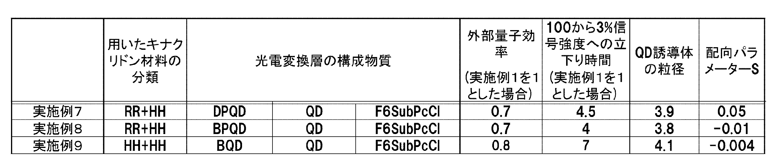
実験2では、実験1と比べてキナクリドン誘導体の結晶粒径を大きくしている。表2から、キナクリドン誘導体の結晶粒径が4.1nm以下の範囲では、外部量子効率および応答性が共に実験1に比べてやや劣るものの、依然として外部量子効率および応答性が共に良好となることがわかった。
(実験3)
次に、有機光電変換層の構成以外は、上記実施例1と同様の方法を用いて光電変換素子(実施例10~11)を作製し、その外部量子効率(EQE)、応答性およびキナクリドン誘導体の結晶粒径を以下のように評価した。ただし、実験3における成膜速度は、0.05nm/秒と0.05nm/秒である。実施例10~11として、実施例1のN-メチル-2,9-ジ-tert-ブチルキナクリドン(BMQD)の代わりに、N-メチルキナクリドン(MMQD)(実施例10)、N,N’-ジメチルキナクリドン(DMQD)(実施例11)を用い、実施例1の2,9-ジ-tert-ブチルキナクリドン(BQD)は実施例10~11の全てで使用せずに、実施例1と同様の方法を用いて光電変換素子を作製した(表3参照)。表3は、HR+HH型構造以外の1種類のキナクリドン誘導体を用いた実施例10~11の評価結果を示したものである。なお、EQEおよび応答性の評価結果は、実施例1の結果を基準値1とした相対値で表している。
次に、有機光電変換層の構成以外は、上記実施例1と同様の方法を用いて光電変換素子(実施例10~11)を作製し、その外部量子効率(EQE)、応答性およびキナクリドン誘導体の結晶粒径を以下のように評価した。ただし、実験3における成膜速度は、0.05nm/秒と0.05nm/秒である。実施例10~11として、実施例1のN-メチル-2,9-ジ-tert-ブチルキナクリドン(BMQD)の代わりに、N-メチルキナクリドン(MMQD)(実施例10)、N,N’-ジメチルキナクリドン(DMQD)(実施例11)を用い、実施例1の2,9-ジ-tert-ブチルキナクリドン(BQD)は実施例10~11の全てで使用せずに、実施例1と同様の方法を用いて光電変換素子を作製した(表3参照)。表3は、HR+HH型構造以外の1種類のキナクリドン誘導体を用いた実施例10~11の評価結果を示したものである。なお、EQEおよび応答性の評価結果は、実施例1の結果を基準値1とした相対値で表している。
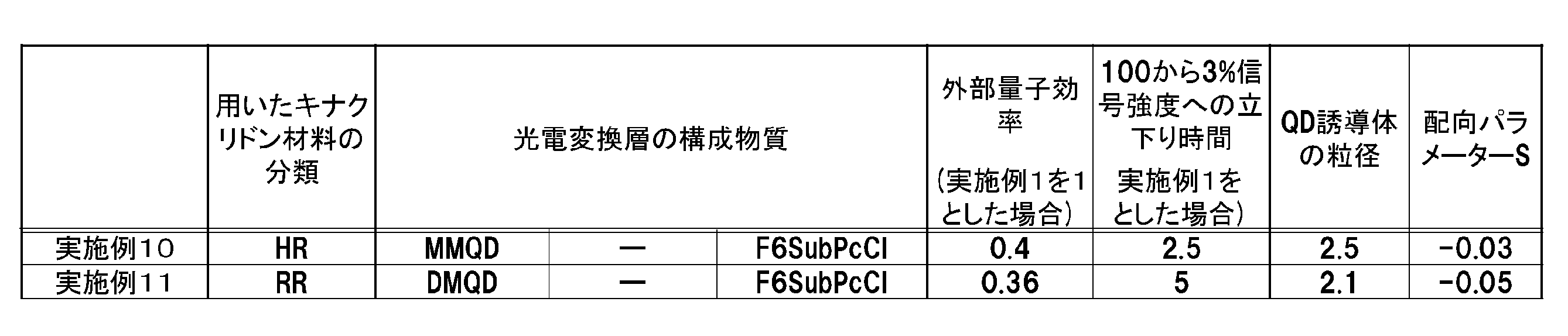
実験3では、1種類のキナクリドン誘導体のみを用いている。表3から、キナクリドン誘導体が1種類の場合でも、キナクリドン誘導体の結晶粒径が約2.5nm以下の範囲で、配向パラメーターSの絶対値が|S|≦0.05であれば、応答性が良好となることがわかった。しかしながら、キナクリドン誘導体が1種類の場合には、キナクリドン誘導体の結晶粒径および配向パラメーターSの値が好条件であっても、外部量子効率が低下することが分かった。
[1-9.比較例]
以下のように、有機光電変換層の構成以外は、上記実施例1と同様の方法を用いて光電変換素子(比較例1~8)を作製し、その外部量子効率(EQE)、応答性およびキナクリドン誘導体の結晶粒径を以下のように評価した。
以下のように、有機光電変換層の構成以外は、上記実施例1と同様の方法を用いて光電変換素子(比較例1~8)を作製し、その外部量子効率(EQE)、応答性およびキナクリドン誘導体の結晶粒径を以下のように評価した。
(実験4)
比較例1~4として、キナクリドン誘導体は、比較例1~3ではキナクリドンのみを、比較例4では2,9-ジメチルキナクリドン(PR122)および2,9-ジ-tert-ブチルキナクリドン(BQD)を用いた。また、サブフタロシアニン誘導体は、比較例1ではホウ素サブフタロシアニンクロリド(SubPc-Cl)を、比較例2ではヘキサフルオロホウ素サブフタロシアニン-4-クロロフェノキシド(SubPc-OPh)を、比較例3および4ではヘキサフルオロホウ素サブフタロシアニンクロリド(F6-SubPc-Cl)を用いた。そして、実施例1と同様の方法を用いて光電変換素子を作製した(表4参照)。表4は、結晶粒径または配向パラメーターSが大き過ぎて応答性が悪い比較例1~4の評価結果を示したものである。なお、EQEおよび応答性の評価結果は、実施例1の結果を基準値1とした相対値で表している。
比較例1~4として、キナクリドン誘導体は、比較例1~3ではキナクリドンのみを、比較例4では2,9-ジメチルキナクリドン(PR122)および2,9-ジ-tert-ブチルキナクリドン(BQD)を用いた。また、サブフタロシアニン誘導体は、比較例1ではホウ素サブフタロシアニンクロリド(SubPc-Cl)を、比較例2ではヘキサフルオロホウ素サブフタロシアニン-4-クロロフェノキシド(SubPc-OPh)を、比較例3および4ではヘキサフルオロホウ素サブフタロシアニンクロリド(F6-SubPc-Cl)を用いた。そして、実施例1と同様の方法を用いて光電変換素子を作製した(表4参照)。表4は、結晶粒径または配向パラメーターSが大き過ぎて応答性が悪い比較例1~4の評価結果を示したものである。なお、EQEおよび応答性の評価結果は、実施例1の結果を基準値1とした相対値で表している。

表4から、キナクリドン誘導体の結晶粒径が4.8nm~6.9nmの範囲、または、配向パラメーターSの絶対値が|S|≦0.15であれば、外部量子効率は良好となることがわかった。しかしながら、実験4の条件の場合には、キナクリドン誘導体の結晶粒径または配向パラメーターSが大き過ぎるため、上記実施例1~11と比べて応答性が極端に低下することが分かった。
(実験5)
比較例5~8として、キナクリドン誘導体は、比較例5では2,9-ジ-tert-ブチルキナクリドン(BQD)のみを、比較例6ではN,N’-ジメチルキナクリドン(DMQD)および2,9-ジ-tert-ブチルキナクリドン(BQD)を、比較例7ではN,N’-ジフェニルキナクリドン(DPQD)および2,9-ジ-tert-ブチルキナクリドン(BQD)を、比較例8では2,9-ジエチルキナクリドン(EQD)および2,9-ジ-tert-ブチルキナクリドン(BQD)を用いた。また、サブフタロシアニン誘導体は、比較例5~8の全てでヘキサフルオロホウ素サブフタロシアニンクロリド(F6-SubPc-Cl)を用いた。そして、実施例1と同様の方法を用いて光電変換素子を作製した(表5参照)。表5は、結晶粒径が小さ過ぎて応答性が悪い比較例5~8の評価結果を示したものである。なお、EQEおよび応答性の評価結果は、実施例1の結果を基準値1とした相対値で表している。
比較例5~8として、キナクリドン誘導体は、比較例5では2,9-ジ-tert-ブチルキナクリドン(BQD)のみを、比較例6ではN,N’-ジメチルキナクリドン(DMQD)および2,9-ジ-tert-ブチルキナクリドン(BQD)を、比較例7ではN,N’-ジフェニルキナクリドン(DPQD)および2,9-ジ-tert-ブチルキナクリドン(BQD)を、比較例8では2,9-ジエチルキナクリドン(EQD)および2,9-ジ-tert-ブチルキナクリドン(BQD)を用いた。また、サブフタロシアニン誘導体は、比較例5~8の全てでヘキサフルオロホウ素サブフタロシアニンクロリド(F6-SubPc-Cl)を用いた。そして、実施例1と同様の方法を用いて光電変換素子を作製した(表5参照)。表5は、結晶粒径が小さ過ぎて応答性が悪い比較例5~8の評価結果を示したものである。なお、EQEおよび応答性の評価結果は、実施例1の結果を基準値1とした相対値で表している。
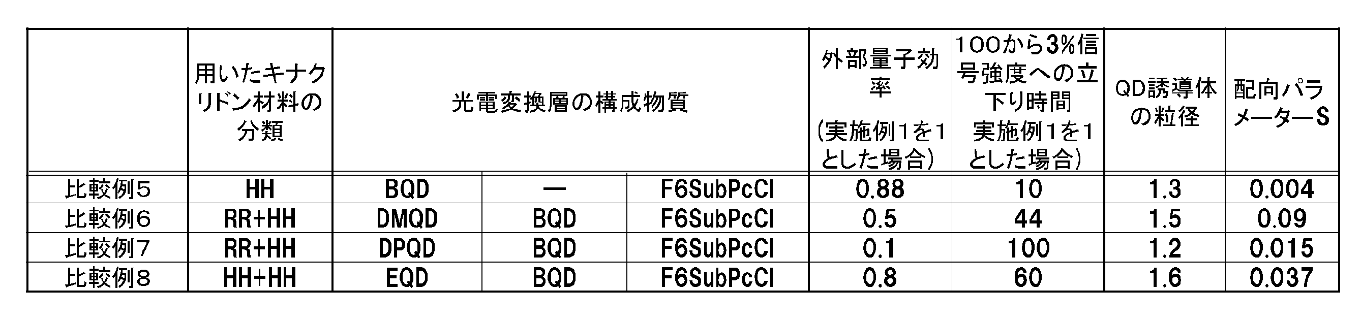
表5の比較例5~8より、キナクリドン誘導体の結晶粒径が1.6nm以下の場合は、配向パラメーターSがS=0に近い値であっても、キナクリドン誘導体の結晶粒径が小さ過ぎるため、上記実施例1~11と比べて応答性が低下することがわかった。
以上の実験1~5の結果より、光電変換素子を構成する光電変換層に、ランダム配向かつ結晶粒径が約2nm~5nmの範囲のキナクリドン誘導体とサブフタロシアニン誘導体とが含まれていることにより、光電変換素子の応答性および外部量子効率が良好になることがわかった。また、実験1~3の結果より、光電変換層に上記キナクリドン誘導体を2種類含むことにより、さらに応答性および外部量子効率を向上させることができることがわかった。
<2.第2実施形態(裏面照射型固体撮像素子)> 図10は、本技術を適用した第2実施形態の固体撮像素子の構成例を示す断面図である。図10を用いて、本実施形態の固体撮像素子900について説明する。
[2-1.裏面照射型の固体撮像素子]
図10は、一例として、CMOSイメージセンサ等の裏面照射型の固体撮像素子900が備える複数の画素のうちの1つの画素901を示している。画素901は、固体撮像素子900の受光表面から深さ方向に、オンチップレンズ(OCL:On-Chip Lens)902、平坦化層903、保護層904、有機光電変換素子10、絶縁膜905、半導体基板(シリコン基板)906、および多層配線層907を有している。また、半導体基板906内には、pn接合を有する2つの無機光電変換部である第1フォトダイオード908および第2フォトダイオード909が形成されている。そして、多層配線層907には、例えば、シリコンで形成された支持基板910が貼り合わせられている。
図10は、一例として、CMOSイメージセンサ等の裏面照射型の固体撮像素子900が備える複数の画素のうちの1つの画素901を示している。画素901は、固体撮像素子900の受光表面から深さ方向に、オンチップレンズ(OCL:On-Chip Lens)902、平坦化層903、保護層904、有機光電変換素子10、絶縁膜905、半導体基板(シリコン基板)906、および多層配線層907を有している。また、半導体基板906内には、pn接合を有する2つの無機光電変換部である第1フォトダイオード908および第2フォトダイオード909が形成されている。そして、多層配線層907には、例えば、シリコンで形成された支持基板910が貼り合わせられている。
半導体基板906の裏面側(図10中の半導体基板906の上側)には、光が入射される受光面が形成され、半導体基板906の表面側(図10中の半導体基板906の下側)には、読み出し回路等を含む回路が形成される。すなわち画素901は、半導体基板906の裏面側に受光面を有し、半導体基板906の表面側に回路形成面を有する。半導体基板906は、例えば、第1導電型をp型、第2導電型をn型として、p型またはn型のいずれの半導体で構成されてもよい。
本実施形態の半導体基板906内では、半導体基板906の裏面側から深さ方向(図10中の下方向)に向かって、まず第1フォトダイオード908が形成され、次に第2フォトダイオード909が形成されている。図10においては、第1フォトダイオード908が青色(B)用となり、第2フォトダイオード909が赤色(R)用となる。
第1フォトダイオード908および第2フォトダイオード909が形成された半導体基板906の裏面上部には、第1電極(下部電極)11、第1バッファ層12、有機光電変換層13、第2バッファ層14、および第2電極(上部電極)15、がこの順で積層された有機光電変換素子10が配されている。本実施形態の固体撮像素子900では、有機光電変換素子10が緑色(G)用となる。有機光電変換素子10内の第1電極11および第2電極は、例えば、酸化インジウム錫膜、酸化インジウム亜鉛膜等の透明導電膜で形成されてよい。なお、有機光電変換層13は、入射光を光電変換するための光吸収層であり、可視波長では結晶質シリコン(Si)であることが一般的である。
色の組み合わせとして、本実施形態の固体撮像素子900では、有機光電変換素子10を緑色、第1フォトダイオード908を青色、第2フォトダイオード909を赤色としたが、その他の色の組み合わせも可能である。例えば、有機光電変換素子10を赤色または青色とし、第1フォトダイオード908および第2フォトダイオード909を、その他の対応する色に設定することができる。この場合、色に応じて第1フォトダイオード908および第2フォトダイオード909の深さ方向の位置が設定される。
さらに、青色用の有機光電変換素子10B、緑色用の有機光電変換素子10Gおよび赤色用の有機光電変換素子10Rに加えて、紫外光用の有機光電変換素子10UVおよび/または赤外光用の有機光電変換素子10IRを、本技術に係る第2の実施形態の固体撮像素子(裏面照射型の固体撮像素子および表面照射型の固体撮像素子)に適用してもよい。紫外光用の有機光電変換素子10UVおよび/または赤外光用の有機光電変換素子10IRを設けることで、可視光領域以外の波長の光を検出することが可能となる。
画素901内には、第1電極11に接続される配線911と第2電極15に接続される配線(図示せず)が形成される。配線911と第2電極15に接続される配線としては、例えば、Siとの短絡を抑制するために、SiO2またはSiN絶縁層を周辺に有するタングステン(W)プラグ、あるいは、イオン注入による半導体層等により形成することができる。本実施形態の固体撮像素子900では、信号電荷を正孔(ホール)としているので、配線911は、イオン注入による半導体層で形成する場合、p型半導体層となる。第2電極15に接続される配線は、第2電極15が電子を引き抜くのでn型半導体層を用いることができる。
本実施形態では、半導体基板906内の表面側に電荷蓄積用のn型領域912が形成される。このn型領域910は、有機光電変換素子10のフローティングディフージョン部として機能する。
半導体基板906の裏面上の絶縁膜905としては、負の固定電荷を有する膜を用いることができる。負の固定電荷を有する膜としては、例えば、ハフニウム酸化膜を用いることができる。すなわち、絶縁膜905は、半導体基板906の裏面側より順次シリコン酸化膜、ハフニウム酸化膜およびシリコン酸化膜を成膜した3層構造となるように形成されてもよい。
また、第1フォトダイオード908および第2フォトダイオード909を用いないで、3つの光電変換素子、すなわち、青色用の有機光電変換素子10B、緑色用の有機光電変換素子10Gおよび赤色用の有機光電変換素子10Rを、本技術に係る第2の実施形態の固体撮像素子(裏面照射型の固体撮像素子および表面照射型の固体撮像素子)に適用してもよい。赤の波長光で光電変換する有機光電変換素子10Rとしては、例えば、フタロシアニン系色素を含む有機光電変換材料を用いることができる。緑の波長光で光電変換する有機光電変換素子10Gとしては、例えば、ローダーミン系色素、メラシアニン系色素、キナクリドン等を含む有機光電変換材料を用いることができる。青の波長光で光電変換する有機光電変換素子10Bとしては、例えば、クマリン系色素、トリス-8-ヒドリキシキノリンAl(Alq3)、メラシアニン系色素等を含む有機光電変換材料を用いることができる。
[2-2.表面照射型の固体撮像素子]
本技術に係る第2実施形態の固体撮像素子は、上述の裏面照射型の固体撮像素子900だけではなく、表面照射型の固体撮像素子にも適用することができる。
本技術に係る第2実施形態の固体撮像素子は、上述の裏面照射型の固体撮像素子900だけではなく、表面照射型の固体撮像素子にも適用することができる。
表面照射型の固体撮像素子の構成例は、半導体基板906の下部に多層配線層910が形成されている裏面照射型の固体撮像素子900に対し、有機光電変換素子10と半導体基板906との間に多層配線層910が形成されるという点のみが異なる。その他の表面照射型の固体撮像素子の構成は、裏面照射型の固体撮像素子900と同様であるため、ここでは説明を省略する。
<3.第3実施形態(電子装置)>
本技術に係る第3実施形態の電子装置は、本技術に係る第2実施形態の固体撮像素子が搭載され、固体撮像素子が、1次元または2次元に配列された複数の画素毎に、少なくとも、本技術に係る第1実施形態の光電変換素子と、半導体基板とが積層された、電子装置である。本技術に係る第3実施形態の電子装置は、応答性および外部量子効率を向上させた固体撮像素子を備えるので、カラー画像の画質等の性能の向上を図ることができる。
本技術に係る第3実施形態の電子装置は、本技術に係る第2実施形態の固体撮像素子が搭載され、固体撮像素子が、1次元または2次元に配列された複数の画素毎に、少なくとも、本技術に係る第1実施形態の光電変換素子と、半導体基板とが積層された、電子装置である。本技術に係る第3実施形態の電子装置は、応答性および外部量子効率を向上させた固体撮像素子を備えるので、カラー画像の画質等の性能の向上を図ることができる。
<4.本技術を適用した固体撮像素子の使用例>
図11は、イメージセンサとしての本技術に係る第2実施形態の固体撮像素子の使用例を示す図である。
図11は、イメージセンサとしての本技術に係る第2実施形態の固体撮像素子の使用例を示す図である。
上述した第2実施形態の固体撮像素子は、例えば、以下のように、可視光や、赤外光、紫外光、X線等の光をセンシングするさまざまなケースに使用することができる。すなわち、図11に示すように、例えば、鑑賞の用に供される画像を撮影する鑑賞の分野、交通の分野、家電の分野、医療・ヘルスケアの分野、セキュリティの分野、美容の分野、スポーツの分野、農業の分野等において用いられる装置(例えば、上述した第3実施形態の電子装置)に、第2実施形態の固体撮像素子を使用することができる。
具体的には、鑑賞の分野においては、例えば、デジタルカメラやスマートフォン、カメラ機能付きの携帯電話機等の、鑑賞の用に供される画像を撮影するための装置に、第2実施形態の固体撮像素子を使用することができる。
交通の分野においては、例えば、自動停止等の安全運転や、運転者の状態の認識等のために、自動車の前方や後方、周囲、車内等を撮影する車載用センサ、走行車両や道路を監視する監視カメラ、車両間等の測距を行う測距センサ等の、交通の用に供される装置に、第2実施形態の固体撮像素子を使用することができる。
家電の分野においては、例えば、ユーザーのジェスチャを撮影して、そのジェスチャに従った機器操作を行うために、テレビ受像機や冷蔵庫、エアーコンディショナ等の家電に供される装置で、第2実施形態の固体撮像素子を使用することができる。
医療・ヘルスケアの分野においては、例えば、内視鏡や、赤外光の受光による血管撮影を行う装置等の、医療やヘルスケアの用に供される装置に、第2実施形態の固体撮像素子を使用することができる。
セキュリティの分野においては、例えば、防犯用途の監視カメラや、人物認証用途のカメラ等の、セキュリティの用に供される装置に、第2実施形態の固体撮像素子を使用することができる。
美容の分野においては、例えば、肌を撮影する肌測定器や、頭皮を撮影するマイクロスコープ等の、美容の用に供される装置に、第2実施形態の固体撮像素子を使用することができる。
スポーツの分野において、例えば、スポーツ用途等向けのアクションカメラやウェアラプルカメラ等の、スポーツの用に供される装置に、第2実施形態の固体撮像素子を使用することができる。
農業の分野においては、例えば、畑や作物の状態を監視するためのカメラ等の、農業の用に供される装置に、第2実施形態の固体撮像素子を使用することができる。
本開示に係る技術(本技術)は、様々な製品へ応用することができる。以下に、内視鏡手術システムへの応用例と移動体への応用例とについて述べる。
<5.内視鏡手術システムへの応用例>
本開示に係る技術は、内視鏡手術システムに適用することができる。
本開示に係る技術は、内視鏡手術システムに適用することができる。
図12は、本開示に係る技術(本技術)が適用され得る内視鏡手術システムの概略的な構成の一例を示す図である。
図12では、術者(医師)11131が、内視鏡手術システム11000を用いて、患者ベッド11133上の患者11132に手術を行っている様子が図示されている。図示するように、内視鏡手術システム11000は、内視鏡11100と、気腹チューブ11111やエネルギー処置具11112等の、その他の術具11110と、内視鏡11100を支持する支持アーム装置11120と、内視鏡下手術のための各種の装置が搭載されたカート11200と、から構成される。
内視鏡11100は、先端から所定の長さの領域が患者11132の体腔内に挿入される鏡筒11101と、鏡筒11101の基端に接続されるカメラヘッド11102と、から構成される。図示する例では、硬性の鏡筒11101を有するいわゆる硬性鏡として構成される内視鏡11100を図示しているが、内視鏡11100は、軟性の鏡筒を有するいわゆる軟性鏡として構成されてもよい。
鏡筒11101の先端には、対物レンズが嵌め込まれた開口部が設けられている。内視鏡11100には光源装置11203が接続されており、当該光源装置11203によって生成された光が、鏡筒11101の内部に延設されるライトガイドによって当該鏡筒の先端まで導光され、対物レンズを介して患者11132の体腔内の観察対象に向かって照射される。なお、内視鏡11100は、直視鏡であってもよいし、斜視鏡又は側視鏡であってもよい。
カメラヘッド11102の内部には光学系及び撮像素子が設けられており、観察対象からの反射光(観察光)は当該光学系によって当該撮像素子に集光される。当該撮像素子によって観察光が光電変換され、観察光に対応する電気信号、すなわち観察像に対応する画像信号が生成される。当該画像信号は、RAWデータとしてカメラコントロールユニット(CCU: Camera Control Unit)11201に送信される。
CCU11201は、CPU(Central Processing Unit)やGPU(Graphics Processing Unit)等によって構成され、内視鏡11100及び表示装置11202の動作を統括的に制御する。さらに、CCU11201は、カメラヘッド11102から画像信号を受け取り、その画像信号に対して、例えば現像処理(デモザイク処理)等の、当該画像信号に基づく画像を表示するための各種の画像処理を施す。
表示装置11202は、CCU11201からの制御により、当該CCU11201によって画像処理が施された画像信号に基づく画像を表示する。
光源装置11203は、例えばLED(Light Emitting Diode)等の光源から構成され、術部等を撮影する際の照射光を内視鏡11100に供給する。
入力装置11204は、内視鏡手術システム11000に対する入力インタフェースである。ユーザは、入力装置11204を介して、内視鏡手術システム11000に対して各種の情報の入力や指示入力を行うことができる。例えば、ユーザは、内視鏡11100による撮像条件(照射光の種類、倍率及び焦点距離等)を変更する旨の指示等を入力する。
処置具制御装置11205は、組織の焼灼、切開又は血管の封止等のためのエネルギー処置具11112の駆動を制御する。気腹装置11206は、内視鏡11100による視野の確保及び術者の作業空間の確保の目的で、患者11132の体腔を膨らめるために、気腹チューブ11111を介して当該体腔内にガスを送り込む。レコーダ11207は、手術に関する各種の情報を記録可能な装置である。プリンタ11208は、手術に関する各種の情報を、テキスト、画像又はグラフ等各種の形式で印刷可能な装置である。
なお、内視鏡11100に術部を撮影する際の照射光を供給する光源装置11203は、例えばLED、レーザ光源又はこれらの組み合わせによって構成される白色光源から構成することができる。RGBレーザ光源の組み合わせにより白色光源が構成される場合には、各色(各波長)の出力強度及び出力タイミングを高精度に制御することができるため、光源装置11203において撮像画像のホワイトバランスの調整を行うことができる。また、この場合には、RGBレーザ光源それぞれからのレーザ光を時分割で観察対象に照射し、その照射タイミングに同期してカメラヘッド11102の撮像素子の駆動を制御することにより、RGBそれぞれに対応した画像を時分割で撮像することも可能である。当該方法によれば、当該撮像素子にカラーフィルタを設けなくても、カラー画像を得ることができる。
また、光源装置11203は、出力する光の強度を所定の時間ごとに変更するようにその駆動が制御されてもよい。その光の強度の変更のタイミングに同期してカメラヘッド11102の撮像素子の駆動を制御して時分割で画像を取得し、その画像を合成することにより、いわゆる黒つぶれ及び白とびのない高ダイナミックレンジの画像を生成することができる。
また、光源装置11203は、特殊光観察に対応した所定の波長帯域の光を供給可能に構成されてもよい。特殊光観察では、例えば、体組織における光の吸収の波長依存性を利用して、通常の観察時における照射光(すなわち、白色光)に比べて狭帯域の光を照射することにより、粘膜表層の血管等の所定の組織を高コントラストで撮影する、いわゆる狭帯域光観察(Narrow Band Imaging)が行われる。あるいは、特殊光観察では、励起光を照射することにより発生する蛍光により画像を得る蛍光観察が行われてもよい。蛍光観察では、体組織に励起光を照射し当該体組織からの蛍光を観察すること(自家蛍光観察)、又はインドシアニングリーン(ICG)等の試薬を体組織に局注するとともに当該体組織にその試薬の蛍光波長に対応した励起光を照射し蛍光像を得ること等を行うことができる。光源装置11203は、このような特殊光観察に対応した狭帯域光及び/又は励起光を供給可能に構成され得る。
図13は、図12に示すカメラヘッド11102及びCCU11201の機能構成の一例を示すブロック図である。
カメラヘッド11102は、レンズユニット11401と、撮像部11402と、駆動部11403と、通信部11404と、カメラヘッド制御部11405と、を有する。CCU11201は、通信部11411と、画像処理部11412と、制御部11413と、を有する。カメラヘッド11102とCCU11201とは、伝送ケーブル11400によって互いに通信可能に接続されている。
レンズユニット11401は、鏡筒11101との接続部に設けられる光学系である。鏡筒11101の先端から取り込まれた観察光は、カメラヘッド11102まで導光され、当該レンズユニット11401に入射する。レンズユニット11401は、ズームレンズ及びフォーカスレンズを含む複数のレンズが組み合わされて構成される。
撮像部11402は、撮像素子で構成される。撮像部11402を構成する撮像素子は、1つ(いわゆる単板式)であってもよいし、複数(いわゆる多板式)であってもよい。撮像部11402が多板式で構成される場合には、例えば各撮像素子によってRGBそれぞれに対応する画像信号が生成され、それらが合成されることによりカラー画像が得られてもよい。あるいは、撮像部11402は、3D(Dimensional)表示に対応する右目用及び左目用の画像信号をそれぞれ取得するための1対の撮像素子を有するように構成されてもよい。3D表示が行われることにより、術者11131は術部における生体組織の奥行きをより正確に把握することが可能になる。なお、撮像部11402が多板式で構成される場合には、各撮像素子に対応して、レンズユニット11401も複数系統設けられ得る。
また、撮像部11402は、必ずしもカメラヘッド11102に設けられなくてもよい。例えば、撮像部11402は、鏡筒11101の内部に、対物レンズの直後に設けられてもよい。
駆動部11403は、アクチュエータによって構成され、カメラヘッド制御部11405からの制御により、レンズユニット11401のズームレンズ及びフォーカスレンズを光軸に沿って所定の距離だけ移動させる。これにより、撮像部11402による撮像画像の倍率及び焦点が適宜調整され得る。
通信部11404は、CCU11201との間で各種の情報を送受信するための通信装置によって構成される。通信部11404は、撮像部11402から得た画像信号をRAWデータとして伝送ケーブル11400を介してCCU11201に送信する。
また、通信部11404は、CCU11201から、カメラヘッド11102の駆動を制御するための制御信号を受信し、カメラヘッド制御部11405に供給する。当該制御信号には、例えば、撮像画像のフレームレートを指定する旨の情報、撮像時の露出値を指定する旨の情報、並びに/又は撮像画像の倍率及び焦点を指定する旨の情報等、撮像条件に関する情報が含まれる。
なお、上記のフレームレートや露出値、倍率、焦点等の撮像条件は、ユーザによって適宜指定されてもよいし、取得された画像信号に基づいてCCU11201の制御部11413によって自動的に設定されてもよい。後者の場合には、いわゆるAE(Auto Exposure)機能、AF(Auto Focus)機能及びAWB(Auto White Balance)機能が内視鏡11100に搭載されていることになる。
カメラヘッド制御部11405は、通信部11404を介して受信したCCU11201からの制御信号に基づいて、カメラヘッド11102の駆動を制御する。
通信部11411は、カメラヘッド11102との間で各種の情報を送受信するための通信装置によって構成される。通信部11411は、カメラヘッド11102から、伝送ケーブル11400を介して送信される画像信号を受信する。
また、通信部11411は、カメラヘッド11102に対して、カメラヘッド11102の駆動を制御するための制御信号を送信する。画像信号や制御信号は、電気通信や光通信等によって送信することができる。
画像処理部11412は、カメラヘッド11102から送信されたRAWデータである画像信号に対して各種の画像処理を施す。
制御部11413は、内視鏡11100による術部等の撮像、及び、術部等の撮像により得られる撮像画像の表示に関する各種の制御を行う。例えば、制御部11413は、カメラヘッド11102の駆動を制御するための制御信号を生成する。
また、制御部11413は、画像処理部11412によって画像処理が施された画像信号に基づいて、術部等が映った撮像画像を表示装置11202に表示させる。この際、制御部11413は、各種の画像認識技術を用いて撮像画像内における各種の物体を認識してもよい。例えば、制御部11413は、撮像画像に含まれる物体のエッジの形状や色等を検出することにより、鉗子等の術具、特定の生体部位、出血、エネルギー処置具11112の使用時のミスト等を認識することができる。制御部11413は、表示装置11202に撮像画像を表示させる際に、その認識結果を用いて、各種の手術支援情報を当該術部の画像に重畳表示させてもよい。手術支援情報が重畳表示され、術者11131に提示されることにより、術者11131の負担を軽減することや、術者11131が確実に手術を進めることが可能になる。
カメラヘッド11102及びCCU11201を接続する伝送ケーブル11400は、電気信号の通信に対応した電気信号ケーブル、光通信に対応した光ファイバ、又はこれらの複合ケーブルである。
ここで、図示する例では、伝送ケーブル11400を用いて有線で通信が行われていたが、カメラヘッド11102とCCU11201との間の通信は無線で行われてもよい。
以上、本開示に係る技術が適用され得る内視鏡手術システムの一例について説明した。本開示に係る技術は、以上説明した構成のうち、カメラヘッド11102の撮像部11402に適用され得る。具体的には、本技術に係る固体撮像素子は、撮像部11402に適用することができる。撮像部11402に、本開示に係る技術を適用することにより、より鮮明な術部画像を得ることができるため、術者が術部を確実に確認することが可能になる。
なお、ここでは、一例として内視鏡手術システムについて説明したが、本開示に係る技術は、その他、例えば、顕微鏡手術システム等に適用されてもよい。
<6.移動体への応用例>
本開示に係る技術は、自動車、電気自動車、ハイブリッド電気自動車、自動二輪車、自転車、パーソナルモビリティ、飛行機、ドローン、船舶、ロボット等のいずれかの種類の移動体に搭載される装置として実現され得る。
本開示に係る技術は、自動車、電気自動車、ハイブリッド電気自動車、自動二輪車、自転車、パーソナルモビリティ、飛行機、ドローン、船舶、ロボット等のいずれかの種類の移動体に搭載される装置として実現され得る。
図14は、本開示に係る技術が適用され得る移動体制御システムの一例である車両制御システムの概略的な構成例を示すブロック図である。
車両制御システム12000は、通信ネットワーク12001を介して接続された複数の電子制御ユニットを備える。図14に示した例では、車両制御システム12000は、駆動系制御ユニット12010、ボディ系制御ユニット12020、車外情報検出ユニット12030、車内情報検出ユニット12040、及び統合制御ユニット12050を備える。また、統合制御ユニット12050の機能構成として、マイクロコンピュータ12051、音声画像出力部12052、及び車載ネットワークI/F(interface)12053が図示されている。
駆動系制御ユニット12010は、各種プログラムにしたがって車両の駆動系に関連する装置の動作を制御する。例えば、駆動系制御ユニット12010は、内燃機関又は駆動用モータ等の車両の駆動力を発生させるための駆動力発生装置、駆動力を車輪に伝達するための駆動力伝達機構、車両の舵角を調節するステアリング機構、及び、車両の制動力を発生させる制動装置等の制御装置として機能する。
ボディ系制御ユニット12020は、各種プログラムにしたがって車体に装備された各種装置の動作を制御する。例えば、ボディ系制御ユニット12020は、キーレスエントリシステム、スマートキーシステム、パワーウィンドウ装置、あるいは、ヘッドランプ、バックランプ、ブレーキランプ、ウィンカー又はフォグランプ等の各種ランプの制御装置として機能する。この場合、ボディ系制御ユニット12020には、鍵を代替する携帯機から発信される電波又は各種スイッチの信号が入力され得る。ボディ系制御ユニット12020は、これらの電波又は信号の入力を受け付け、車両のドアロック装置、パワーウィンドウ装置、ランプ等を制御する。
車外情報検出ユニット12030は、車両制御システム12000を搭載した車両の外部の情報を検出する。例えば、車外情報検出ユニット12030には、撮像部12031が接続される。車外情報検出ユニット12030は、撮像部12031に車外の画像を撮像させるとともに、撮像された画像を受信する。車外情報検出ユニット12030は、受信した画像に基づいて、人、車、障害物、標識又は路面上の文字等の物体検出処理又は距離検出処理を行ってもよい。
撮像部12031は、光を受光し、その光の受光量に応じた電気信号を出力する光センサである。撮像部12031は、電気信号を画像として出力することもできるし、測距の情報として出力することもできる。また、撮像部12031が受光する光は、可視光であっても良いし、赤外線等の非可視光であっても良い。
車内情報検出ユニット12040は、車内の情報を検出する。車内情報検出ユニット12040には、例えば、運転者の状態を検出する運転者状態検出部12041が接続される。運転者状態検出部12041は、例えば運転者を撮像するカメラを含み、車内情報検出ユニット12040は、運転者状態検出部12041から入力される検出情報に基づいて、運転者の疲労度合い又は集中度合いを算出してもよいし、運転者が居眠りをしていないかを判別してもよい。
マイクロコンピュータ12051は、車外情報検出ユニット12030又は車内情報検出ユニット12040で取得される車内外の情報に基づいて、駆動力発生装置、ステアリング機構又は制動装置の制御目標値を演算し、駆動系制御ユニット12010に対して制御指令を出力することができる。例えば、マイクロコンピュータ12051は、車両の衝突回避あるいは衝撃緩和、車間距離に基づく追従走行、車速維持走行、車両の衝突警告、又は車両のレーン逸脱警告等を含むADAS(Advanced Driver Assistance System)の機能実現を目的とした協調制御を行うことができる。
また、マイクロコンピュータ12051は、車外情報検出ユニット12030又は車内情報検出ユニット12040で取得される車両の周囲の情報に基づいて駆動力発生装置、ステアリング機構又は制動装置等を制御することにより、運転者の操作に拠らずに自律的に走行する自動運転等を目的とした協調制御を行うことができる。
また、マイクロコンピュータ12051は、車外情報検出ユニット12030で取得される車外の情報に基づいて、ボディ系制御ユニット12020に対して制御指令を出力することができる。例えば、マイクロコンピュータ12051は、車外情報検出ユニット12030で検知した先行車又は対向車の位置に応じてヘッドランプを制御し、ハイビームをロービームに切り替える等の防眩を図ることを目的とした協調制御を行うことができる。
音声画像出力部12052は、車両の搭乗者又は車外に対して、視覚的又は聴覚的に情報を通知することが可能な出力装置へ音声及び画像のうちの少なくとも一方の出力信号を送信する。図14の例では、出力装置として、オーディオスピーカ12061、表示部12062及びインストルメントパネル12063が例示されている。表示部12062は、例えば、オンボードディスプレイ及びヘッドアップディスプレイの少なくとも一つを含んでいてもよい。
図15は、撮像部12031の設置位置の例を示す図である。
図15では、車両12100は、撮像部12031として、撮像部12101,12102,12103,12104,12105を有する。
撮像部12101,12102,12103,12104,12105は、例えば、車両12100のフロントノーズ、サイドミラー、リアバンパ、バックドア及び車室内のフロントガラスの上部等の位置に設けられる。フロントノーズに備えられる撮像部12101及び車室内のフロントガラスの上部に備えられる撮像部12105は、主として車両12100の前方の画像を取得する。サイドミラーに備えられる撮像部12102,12103は、主として車両12100の側方の画像を取得する。リアバンパ又はバックドアに備えられる撮像部12104は、主として車両12100の後方の画像を取得する。撮像部12101及び12105で取得される前方の画像は、主として先行車両又は、歩行者、障害物、信号機、交通標識又は車線等の検出に用いられる。
なお、図15には、撮像部12101ないし12104の撮影範囲の一例が示されている。撮像範囲12111は、フロントノーズに設けられた撮像部12101の撮像範囲を示し、撮像範囲12112,12113は、それぞれサイドミラーに設けられた撮像部12102,12103の撮像範囲を示し、撮像範囲12114は、リアバンパ又はバックドアに設けられた撮像部12104の撮像範囲を示す。例えば、撮像部12101ないし12104で撮像された画像データが重ね合わせられることにより、車両12100を上方から見た俯瞰画像が得られる。
撮像部12101ないし12104の少なくとも1つは、距離情報を取得する機能を有していてもよい。例えば、撮像部12101ないし12104の少なくとも1つは、複数の撮像素子からなるステレオカメラであってもよいし、位相差検出用の画素を有する撮像素子であってもよい。
例えば、マイクロコンピュータ12051は、撮像部12101ないし12104から得られた距離情報を基に、撮像範囲12111ないし12114内における各立体物までの距離と、この距離の時間的変化(車両12100に対する相対速度)を求めることにより、特に車両12100の進行路上にある最も近い立体物で、車両12100と略同じ方向に所定の速度(例えば、0km/h以上)で走行する立体物を先行車として抽出することができる。さらに、マイクロコンピュータ12051は、先行車の手前に予め確保すべき車間距離を設定し、自動ブレーキ制御(追従停止制御も含む)や自動加速制御(追従発進制御も含む)等を行うことができる。このように運転者の操作に拠らずに自律的に走行する自動運転等を目的とした協調制御を行うことができる。
例えば、マイクロコンピュータ12051は、撮像部12101ないし12104から得られた距離情報を元に、立体物に関する立体物データを、2輪車、普通車両、大型車両、歩行者、電柱等その他の立体物に分類して抽出し、障害物の自動回避に用いることができる。例えば、マイクロコンピュータ12051は、車両12100の周辺の障害物を、車両12100のドライバが視認可能な障害物と視認困難な障害物とに識別する。そして、マイクロコンピュータ12051は、各障害物との衝突の危険度を示す衝突リスクを判断し、衝突リスクが設定値以上で衝突可能性がある状況であるときには、オーディオスピーカ12061や表示部12062を介してドライバに警報を出力することや、駆動系制御ユニット12010を介して強制減速や回避操舵を行うことで、衝突回避のための運転支援を行うことができる。
撮像部12101ないし12104の少なくとも1つは、赤外線を検出する赤外線カメラであってもよい。例えば、マイクロコンピュータ12051は、撮像部12101ないし12104の撮像画像中に歩行者が存在するか否かを判定することで歩行者を認識することができる。かかる歩行者の認識は、例えば赤外線カメラとしての撮像部12101ないし12104の撮像画像における特徴点を抽出する手順と、物体の輪郭を示す一連の特徴点にパターンマッチング処理を行って歩行者か否かを判別する手順によって行われる。マイクロコンピュータ12051が、撮像部12101ないし12104の撮像画像中に歩行者が存在すると判定し、歩行者を認識すると、音声画像出力部12052は、当該認識された歩行者に強調のための方形輪郭線を重畳表示するように、表示部12062を制御する。また、音声画像出力部12052は、歩行者を示すアイコン等を所望の位置に表示するように表示部12062を制御してもよい。
以上、本開示に係る技術が適用され得る車両制御システムの一例について説明した。本開示に係る技術は、以上説明した構成のうち、撮像部12031(撮像部12101、12102、12103、12104及び12105)に適用され得る。具体的には、本技術に係る固体撮像素子は、撮像部12031(撮像部12101、12102、12103、12104及び12105)に適用することができる。撮像部12031(撮像部12101、12102、12103、12104及び12105)に、本開示に係る技術を適用することにより、より見やすい撮影画像を得ることができるため、ドライバの疲労を軽減することが可能になる。
なお、本技術に係る実施形態は、上述した実施形態に限定されるものではなく、本技術の要旨を逸脱しない範囲において種々の変更が可能である。
また、本明細書に記載された効果はあくまでも例示であって限定されるものではなく、また他の効果があってもよい。
また、本技術は、以下のような構成を取ることができる。
[1]
第1電極と第2電極とに挟まれた有機光電変換層を備え、該有機光電変換層は、キナクリドン誘導体およびサブフタロシアニン誘導体の有機分子を含み、
前記有機分子のうちの少なくとも前記キナクリドン誘導体がランダム配向である光電変換素子。
[2]
前記キナクリドン誘導体の結晶粒径が2~5nmである[1]に記載の光電変換素子。
[3]
さらに前記サブフタロシアニン誘導体がランダム配向である[1]に記載の光電変換素子。
[4]
前記ランダム配向は、前記キナクリドン誘導体の遷移双極子モーメントの平均方位と前記有機光電変換層の積層面法線とのなす角度が50°~60°方向の配向である[1]に記載の光電変換素子。
[5]
前記有機分子は、前記キナクリドン誘導体を2種類以上含む[1]に記載の光電変換素子。
[6]
前記キナクリドン誘導体は、2,9-ジエチルキナクリドン(EQD)、2,9-ジ-tert-ブチルキナクリドン(BQD)、N,N’-ジメチルキナクリドン(DMQD)、N,N’-ジフェニルキナクリドン(DPQD)、N,N’-ジフェニル-2,9-ジ-tert-ブチルキナクリドン(BPQD)、N-メチルキナクリドン(MMQD)、N-メチル-2,9-ジメチルキナクリドン(TMQD)、N-メチル-2,9-ジ-tert-ブチルキナクリドン(BMQD)およびN-フェニルキナクリドン(MPQD)のうち、少なくとも2種を含む[1]に記載の光電変換素子。
[7]
前記サブフタロシアニン誘導体は、ヘキサフルオロホウ素サブフタロシアニンクロリド(F6-SubPc-Cl)、ヘキサフルオロホウ素サブフタロシアニン-4-クロロフェノキシド(F6-SubPc-OPh),ホウ素サブフタロシアニンクロリド(SubPc-Cl), および ヘキサフルオロホウ素サブフタロシアニン-4-クロロフェノキシド(SubPc-OPh)のいずれか1種である[1]に記載の光電変換素子。
[8]
1次元または2次元に配列された複数の画素毎に、
少なくとも、[1]に記載の光電変換素子と、半導体基板とが積層された、固体撮像素子。
[9]
[8]に記載の固体撮像素子を備えた、電子装置。
[1]
第1電極と第2電極とに挟まれた有機光電変換層を備え、該有機光電変換層は、キナクリドン誘導体およびサブフタロシアニン誘導体の有機分子を含み、
前記有機分子のうちの少なくとも前記キナクリドン誘導体がランダム配向である光電変換素子。
[2]
前記キナクリドン誘導体の結晶粒径が2~5nmである[1]に記載の光電変換素子。
[3]
さらに前記サブフタロシアニン誘導体がランダム配向である[1]に記載の光電変換素子。
[4]
前記ランダム配向は、前記キナクリドン誘導体の遷移双極子モーメントの平均方位と前記有機光電変換層の積層面法線とのなす角度が50°~60°方向の配向である[1]に記載の光電変換素子。
[5]
前記有機分子は、前記キナクリドン誘導体を2種類以上含む[1]に記載の光電変換素子。
[6]
前記キナクリドン誘導体は、2,9-ジエチルキナクリドン(EQD)、2,9-ジ-tert-ブチルキナクリドン(BQD)、N,N’-ジメチルキナクリドン(DMQD)、N,N’-ジフェニルキナクリドン(DPQD)、N,N’-ジフェニル-2,9-ジ-tert-ブチルキナクリドン(BPQD)、N-メチルキナクリドン(MMQD)、N-メチル-2,9-ジメチルキナクリドン(TMQD)、N-メチル-2,9-ジ-tert-ブチルキナクリドン(BMQD)およびN-フェニルキナクリドン(MPQD)のうち、少なくとも2種を含む[1]に記載の光電変換素子。
[7]
前記サブフタロシアニン誘導体は、ヘキサフルオロホウ素サブフタロシアニンクロリド(F6-SubPc-Cl)、ヘキサフルオロホウ素サブフタロシアニン-4-クロロフェノキシド(F6-SubPc-OPh),ホウ素サブフタロシアニンクロリド(SubPc-Cl), および ヘキサフルオロホウ素サブフタロシアニン-4-クロロフェノキシド(SubPc-OPh)のいずれか1種である[1]に記載の光電変換素子。
[8]
1次元または2次元に配列された複数の画素毎に、
少なくとも、[1]に記載の光電変換素子と、半導体基板とが積層された、固体撮像素子。
[9]
[8]に記載の固体撮像素子を備えた、電子装置。
10 光電変換素子
11 第1電極
12 第1バッファ層
13 有機光電変換層
14 第2バッファ層
15 第2電極
20、51 キナクリドン(QD)
21、22、23、26、27 層
41 形状異方性粒子
52 軸
900 固体撮像素子
901 画素
902 オンチップレンズ(OCL)
903 平坦化層
904 保護層
905 絶縁膜
906 半導体基板
907 多層配線層
908、909 フォトダイオード
910 支持基板
911 配線
912 n型領域
11 第1電極
12 第1バッファ層
13 有機光電変換層
14 第2バッファ層
15 第2電極
20、51 キナクリドン(QD)
21、22、23、26、27 層
41 形状異方性粒子
52 軸
900 固体撮像素子
901 画素
902 オンチップレンズ(OCL)
903 平坦化層
904 保護層
905 絶縁膜
906 半導体基板
907 多層配線層
908、909 フォトダイオード
910 支持基板
911 配線
912 n型領域
Claims (9)
- 第1電極と第2電極とに挟まれた有機光電変換層を備え、該有機光電変換層は、キナクリドン誘導体およびサブフタロシアニン誘導体の有機分子を含み、
前記有機分子のうちの少なくとも前記キナクリドン誘導体がランダム配向である光電変換素子。 - 前記キナクリドン誘導体の結晶粒径が2~5nmである請求項1に記載の光電変換素子。
- さらに前記サブフタロシアニン誘導体がランダム配向である請求項1に記載の光電変換素子。
- 前記ランダム配向は、前記キナクリドン誘導体の遷移双極子モーメントの平均方位と前記有機光電変換層の積層面法線とのなす角度が50°~60°方向の配向である請求項1に記載の光電変換素子。
- 前記有機分子は、前記キナクリドン誘導体を2種類以上含む請求項1に記載の光電変換素子。
- 前記キナクリドン誘導体は、2,9-ジエチルキナクリドン(EQD)、2,9-ジ-tert-ブチルキナクリドン(BQD)、N,N’-ジメチルキナクリドン(DMQD)、N,N’-ジフェニルキナクリドン(DPQD)、N,N’-ジフェニル-2,9-ジ-tert-ブチルキナクリドン(BPQD)、N-メチルキナクリドン(MMQD)、N-メチル-2,9-ジメチルキナクリドン(TMQD)、N-メチル-2,9-ジ-tert-ブチルキナクリドン(BMQD)およびN-フェニルキナクリドン(MPQD)のうち、少なくとも2種を含む請求項1に記載の光電変換素子。
- 前記サブフタロシアニン誘導体は、ヘキサフルオロホウ素サブフタロシアニンクロリド(F6-SubPc-Cl)、ヘキサフルオロホウ素サブフタロシアニン-4-クロロフェノキシド(F6-SubPc-OPh),ホウ素サブフタロシアニンクロリド(SubPc-Cl), および ヘキサフルオロホウ素サブフタロシアニン-4-クロロフェノキシド(SubPc-OPh)のいずれか1種である請求項1に記載の光電変換素子。
- 1次元または2次元に配列された複数の画素毎に、
少なくとも、請求項1に記載の光電変換素子と、半導体基板とが積層された、固体撮像素子。 - 請求項8に記載の固体撮像素子を備えた、電子装置。
Priority Applications (2)
| Application Number | Priority Date | Filing Date | Title |
|---|---|---|---|
| US16/347,638 US10892301B2 (en) | 2016-11-16 | 2017-10-24 | Photo-electric conversion element, solid-state imaging element, and electronic apparatus |
| US17/119,008 US20210118955A1 (en) | 2016-11-16 | 2020-12-11 | Photo-electric conversion element, solid-state imaging element, and electronic apparatus |
Applications Claiming Priority (2)
| Application Number | Priority Date | Filing Date | Title |
|---|---|---|---|
| JP2016222916A JP2018082022A (ja) | 2016-11-16 | 2016-11-16 | 光電変換素子、固体撮像素子および電子装置 |
| JP2016-222916 | 2016-11-16 |
Related Child Applications (2)
| Application Number | Title | Priority Date | Filing Date |
|---|---|---|---|
| US16/347,638 A-371-Of-International US10892301B2 (en) | 2016-11-16 | 2017-10-24 | Photo-electric conversion element, solid-state imaging element, and electronic apparatus |
| US17/119,008 Continuation US20210118955A1 (en) | 2016-11-16 | 2020-12-11 | Photo-electric conversion element, solid-state imaging element, and electronic apparatus |
Publications (1)
| Publication Number | Publication Date |
|---|---|
| WO2018092523A1 true WO2018092523A1 (ja) | 2018-05-24 |
Family
ID=62146036
Family Applications (1)
| Application Number | Title | Priority Date | Filing Date |
|---|---|---|---|
| PCT/JP2017/038245 Ceased WO2018092523A1 (ja) | 2016-11-16 | 2017-10-24 | 光電変換素子、固体撮像素子および電子装置 |
Country Status (3)
| Country | Link |
|---|---|
| US (2) | US10892301B2 (ja) |
| JP (1) | JP2018082022A (ja) |
| WO (1) | WO2018092523A1 (ja) |
Cited By (3)
| Publication number | Priority date | Publication date | Assignee | Title |
|---|---|---|---|---|
| WO2020012842A1 (ja) * | 2018-07-09 | 2020-01-16 | ソニー株式会社 | 光電変換素子 |
| WO2021044262A1 (ja) * | 2019-09-06 | 2021-03-11 | 株式会社半導体エネルギー研究所 | 発光デバイス、表示装置、電子機器、有機化合物及び照明装置 |
| WO2023176852A1 (ja) * | 2022-03-17 | 2023-09-21 | ソニーセミコンダクタソリューションズ株式会社 | 光電変換素子および光検出装置ならびに光検出システム |
Citations (6)
| Publication number | Priority date | Publication date | Assignee | Title |
|---|---|---|---|---|
| JP2006086493A (ja) * | 2004-03-19 | 2006-03-30 | Fuji Photo Film Co Ltd | 光電変換膜、光電変換素子、及び撮像素子、並びに、これらに電場を印加する方法、及び印加した素子 |
| JP2006245285A (ja) * | 2005-03-03 | 2006-09-14 | Fuji Photo Film Co Ltd | 光電変換膜積層型固体撮像素子 |
| JP2013526082A (ja) * | 2010-05-05 | 2013-06-20 | ザ リージェンツ オブ ザ ユニヴァシティ オブ ミシガン | 有機ドナー‐アクセプタヘテロ接合における励起子解離の改善方法 |
| WO2014073446A1 (ja) * | 2012-11-09 | 2014-05-15 | ソニー株式会社 | 光電変換素子および固体撮像装置ならびに電子機器 |
| JP2015138861A (ja) * | 2014-01-22 | 2015-07-30 | ソニー株式会社 | 固体撮像素子および製造方法、並びに電子機器 |
| JP2015233117A (ja) * | 2014-05-13 | 2015-12-24 | ソニー株式会社 | 光電変換膜、固体撮像素子、および電子機器 |
Family Cites Families (1)
| Publication number | Priority date | Publication date | Assignee | Title |
|---|---|---|---|---|
| US7570292B2 (en) | 2004-03-19 | 2009-08-04 | Fujifilm Corporation | Photoelectric conversion film, photoelectric conversion element, imaging element, method of applying electric field thereto and electric field-applied element |
-
2016
- 2016-11-16 JP JP2016222916A patent/JP2018082022A/ja active Pending
-
2017
- 2017-10-24 US US16/347,638 patent/US10892301B2/en active Active
- 2017-10-24 WO PCT/JP2017/038245 patent/WO2018092523A1/ja not_active Ceased
-
2020
- 2020-12-11 US US17/119,008 patent/US20210118955A1/en not_active Abandoned
Patent Citations (6)
| Publication number | Priority date | Publication date | Assignee | Title |
|---|---|---|---|---|
| JP2006086493A (ja) * | 2004-03-19 | 2006-03-30 | Fuji Photo Film Co Ltd | 光電変換膜、光電変換素子、及び撮像素子、並びに、これらに電場を印加する方法、及び印加した素子 |
| JP2006245285A (ja) * | 2005-03-03 | 2006-09-14 | Fuji Photo Film Co Ltd | 光電変換膜積層型固体撮像素子 |
| JP2013526082A (ja) * | 2010-05-05 | 2013-06-20 | ザ リージェンツ オブ ザ ユニヴァシティ オブ ミシガン | 有機ドナー‐アクセプタヘテロ接合における励起子解離の改善方法 |
| WO2014073446A1 (ja) * | 2012-11-09 | 2014-05-15 | ソニー株式会社 | 光電変換素子および固体撮像装置ならびに電子機器 |
| JP2015138861A (ja) * | 2014-01-22 | 2015-07-30 | ソニー株式会社 | 固体撮像素子および製造方法、並びに電子機器 |
| JP2015233117A (ja) * | 2014-05-13 | 2015-12-24 | ソニー株式会社 | 光電変換膜、固体撮像素子、および電子機器 |
Cited By (6)
| Publication number | Priority date | Publication date | Assignee | Title |
|---|---|---|---|---|
| WO2020012842A1 (ja) * | 2018-07-09 | 2020-01-16 | ソニー株式会社 | 光電変換素子 |
| WO2021044262A1 (ja) * | 2019-09-06 | 2021-03-11 | 株式会社半導体エネルギー研究所 | 発光デバイス、表示装置、電子機器、有機化合物及び照明装置 |
| JPWO2021044262A1 (ja) * | 2019-09-06 | 2021-03-11 | ||
| JP7538132B2 (ja) | 2019-09-06 | 2024-08-21 | 株式会社半導体エネルギー研究所 | 有機化合物、発光デバイス用材料、発光デバイス、発光装置、電子機器及び照明装置 |
| US12534459B2 (en) | 2019-09-06 | 2026-01-27 | Semiconductor Energy Laboratory Co., Ltd. | Light-emitting device, display device, electronic device, organic compound, and lighting device |
| WO2023176852A1 (ja) * | 2022-03-17 | 2023-09-21 | ソニーセミコンダクタソリューションズ株式会社 | 光電変換素子および光検出装置ならびに光検出システム |
Also Published As
| Publication number | Publication date |
|---|---|
| US10892301B2 (en) | 2021-01-12 |
| US20190319072A1 (en) | 2019-10-17 |
| JP2018082022A (ja) | 2018-05-24 |
| US20210118955A1 (en) | 2021-04-22 |
Similar Documents
| Publication | Publication Date | Title |
|---|---|---|
| JP7014785B2 (ja) | 光電変換素子および撮像素子 | |
| CN110226228B (zh) | 光接收器件、光接收器件制造方法、摄像器件和电子设备 | |
| US10580821B2 (en) | Light-receiving element, manufacturing method of the same, imaging device, and electronic apparatus | |
| CN109983581A (zh) | 光接收装置、摄像装置和电子设备 | |
| JPWO2020026851A1 (ja) | 撮像素子および撮像装置 | |
| JPWO2020022421A1 (ja) | 光電変換素子 | |
| EP3923331A1 (en) | Imaging device and imaging system | |
| JP7562507B2 (ja) | 固体撮像素子および固体撮像素子の製造方法、並びに固体撮像装置 | |
| JP2018098343A (ja) | 撮像素子、金属薄膜フィルタ、電子機器 | |
| US20210118955A1 (en) | Photo-electric conversion element, solid-state imaging element, and electronic apparatus | |
| WO2018180575A1 (ja) | 固体撮像素子、電子機器、並びに製造方法 | |
| JP2018206837A (ja) | 固体撮像装置および固体撮像装置の製造方法、並びに電子機器 | |
| CN116420234A (zh) | 光电转换元件、光电探测器、光电探测系统、电子设备及移动体 | |
| US20220415958A1 (en) | Solid-state imaging element and electronic device | |
| JPWO2019098315A1 (ja) | 光電変換素子および固体撮像装置 | |
| US12529834B2 (en) | Multilayer film and imaging element | |
| EP3404715B1 (en) | Light receiving element, method for manufacturing light receiving element, image capturing element and electronic device | |
| WO2022131101A1 (ja) | 光電変換素子、光検出装置、光検出システム、電子機器および移動体 | |
| WO2020195935A1 (ja) | 固体撮像素子および固体撮像素子の製造方法、光電変換素子、撮像装置、並びに電子機器 | |
| JP7366936B2 (ja) | 酸化物半導体膜のエッチング方法 | |
| WO2022131090A1 (ja) | 光検出装置、光検出システム、電子機器および移動体 | |
| JP7291082B2 (ja) | 撮像装置 | |
| WO2021246320A1 (ja) | 光電変換素子および撮像装置 | |
| WO2020012842A1 (ja) | 光電変換素子 | |
| US20250185394A1 (en) | Solid-state imaging device and electronic apparatus |
Legal Events
| Date | Code | Title | Description |
|---|---|---|---|
| 121 | Ep: the epo has been informed by wipo that ep was designated in this application |
Ref document number: 17872074 Country of ref document: EP Kind code of ref document: A1 |
|
| NENP | Non-entry into the national phase |
Ref country code: DE |
|
| 122 | Ep: pct application non-entry in european phase |
Ref document number: 17872074 Country of ref document: EP Kind code of ref document: A1 |