WO2018084282A1 - 蛍光体含有フィルムおよびバックライトユニット - Google Patents
蛍光体含有フィルムおよびバックライトユニット Download PDFInfo
- Publication number
- WO2018084282A1 WO2018084282A1 PCT/JP2017/039930 JP2017039930W WO2018084282A1 WO 2018084282 A1 WO2018084282 A1 WO 2018084282A1 JP 2017039930 W JP2017039930 W JP 2017039930W WO 2018084282 A1 WO2018084282 A1 WO 2018084282A1
- Authority
- WO
- WIPO (PCT)
- Prior art keywords
- layer
- phosphor
- film
- light
- meth
- Prior art date
- Legal status (The legal status is an assumption and is not a legal conclusion. Google has not performed a legal analysis and makes no representation as to the accuracy of the status listed.)
- Ceased
Links
Images



Classifications
-
- B—PERFORMING OPERATIONS; TRANSPORTING
- B32—LAYERED PRODUCTS
- B32B—LAYERED PRODUCTS, i.e. PRODUCTS BUILT-UP OF STRATA OF FLAT OR NON-FLAT, e.g. CELLULAR OR HONEYCOMB, FORM
- B32B27/00—Layered products comprising a layer of synthetic resin
- B32B27/18—Layered products comprising a layer of synthetic resin characterised by the use of special additives
- B32B27/20—Layered products comprising a layer of synthetic resin characterised by the use of special additives using fillers, pigments, thixotroping agents
-
- G—PHYSICS
- G02—OPTICS
- G02B—OPTICAL ELEMENTS, SYSTEMS OR APPARATUS
- G02B5/00—Optical elements other than lenses
- G02B5/20—Filters
-
- B—PERFORMING OPERATIONS; TRANSPORTING
- B32—LAYERED PRODUCTS
- B32B—LAYERED PRODUCTS, i.e. PRODUCTS BUILT-UP OF STRATA OF FLAT OR NON-FLAT, e.g. CELLULAR OR HONEYCOMB, FORM
- B32B27/00—Layered products comprising a layer of synthetic resin
- B32B27/06—Layered products comprising a layer of synthetic resin as the main or only constituent of a layer, which is next to another layer of the same or of a different material
-
- B—PERFORMING OPERATIONS; TRANSPORTING
- B32—LAYERED PRODUCTS
- B32B—LAYERED PRODUCTS, i.e. PRODUCTS BUILT-UP OF STRATA OF FLAT OR NON-FLAT, e.g. CELLULAR OR HONEYCOMB, FORM
- B32B27/00—Layered products comprising a layer of synthetic resin
- B32B27/18—Layered products comprising a layer of synthetic resin characterised by the use of special additives
-
- B—PERFORMING OPERATIONS; TRANSPORTING
- B32—LAYERED PRODUCTS
- B32B—LAYERED PRODUCTS, i.e. PRODUCTS BUILT-UP OF STRATA OF FLAT OR NON-FLAT, e.g. CELLULAR OR HONEYCOMB, FORM
- B32B3/00—Layered products comprising a layer with external or internal discontinuities or unevennesses, or a layer of non-planar shape; Layered products comprising a layer having particular features of form
- B32B3/26—Layered products comprising a layer with external or internal discontinuities or unevennesses, or a layer of non-planar shape; Layered products comprising a layer having particular features of form characterised by a particular shape of the outline of the cross-section of a continuous layer; characterised by a layer with cavities or internal voids ; characterised by an apertured layer
- B32B3/30—Layered products comprising a layer with external or internal discontinuities or unevennesses, or a layer of non-planar shape; Layered products comprising a layer having particular features of form characterised by a particular shape of the outline of the cross-section of a continuous layer; characterised by a layer with cavities or internal voids ; characterised by an apertured layer characterised by a layer formed with recesses or projections, e.g. hollows, grooves, protuberances, ribs
-
- C—CHEMISTRY; METALLURGY
- C09—DYES; PAINTS; POLISHES; NATURAL RESINS; ADHESIVES; COMPOSITIONS NOT OTHERWISE PROVIDED FOR; APPLICATIONS OF MATERIALS NOT OTHERWISE PROVIDED FOR
- C09K—MATERIALS FOR MISCELLANEOUS APPLICATIONS, NOT PROVIDED FOR ELSEWHERE
- C09K11/00—Luminescent materials, e.g. electroluminescent or chemiluminescent
- C09K11/02—Use of particular materials as binders, particle coatings or suspension media therefor
-
- C—CHEMISTRY; METALLURGY
- C09—DYES; PAINTS; POLISHES; NATURAL RESINS; ADHESIVES; COMPOSITIONS NOT OTHERWISE PROVIDED FOR; APPLICATIONS OF MATERIALS NOT OTHERWISE PROVIDED FOR
- C09K—MATERIALS FOR MISCELLANEOUS APPLICATIONS, NOT PROVIDED FOR ELSEWHERE
- C09K11/00—Luminescent materials, e.g. electroluminescent or chemiluminescent
- C09K11/08—Luminescent materials, e.g. electroluminescent or chemiluminescent containing inorganic luminescent materials
-
- F—MECHANICAL ENGINEERING; LIGHTING; HEATING; WEAPONS; BLASTING
- F21—LIGHTING
- F21S—NON-PORTABLE LIGHTING DEVICES; SYSTEMS THEREOF; VEHICLE LIGHTING DEVICES SPECIALLY ADAPTED FOR VEHICLE EXTERIORS
- F21S2/00—Systems of lighting devices, not provided for in main groups F21S4/00 - F21S10/00 or F21S19/00, e.g. of modular construction
-
- G—PHYSICS
- G02—OPTICS
- G02F—OPTICAL DEVICES OR ARRANGEMENTS FOR THE CONTROL OF LIGHT BY MODIFICATION OF THE OPTICAL PROPERTIES OF THE MEDIA OF THE ELEMENTS INVOLVED THEREIN; NON-LINEAR OPTICS; FREQUENCY-CHANGING OF LIGHT; OPTICAL LOGIC ELEMENTS; OPTICAL ANALOGUE/DIGITAL CONVERTERS
- G02F1/00—Devices or arrangements for the control of the intensity, colour, phase, polarisation or direction of light arriving from an independent light source, e.g. switching, gating or modulating; Non-linear optics
- G02F1/01—Devices or arrangements for the control of the intensity, colour, phase, polarisation or direction of light arriving from an independent light source, e.g. switching, gating or modulating; Non-linear optics for the control of the intensity, phase, polarisation or colour
- G02F1/13—Devices or arrangements for the control of the intensity, colour, phase, polarisation or direction of light arriving from an independent light source, e.g. switching, gating or modulating; Non-linear optics for the control of the intensity, phase, polarisation or colour based on liquid crystals, e.g. single liquid crystal display cells
- G02F1/133—Constructional arrangements; Operation of liquid crystal cells; Circuit arrangements
- G02F1/1333—Constructional arrangements; Manufacturing methods
- G02F1/1335—Structural association of cells with optical devices, e.g. polarisers or reflectors
- G02F1/1336—Illuminating devices
-
- B—PERFORMING OPERATIONS; TRANSPORTING
- B32—LAYERED PRODUCTS
- B32B—LAYERED PRODUCTS, i.e. PRODUCTS BUILT-UP OF STRATA OF FLAT OR NON-FLAT, e.g. CELLULAR OR HONEYCOMB, FORM
- B32B2307/00—Properties of the layers or laminate
- B32B2307/40—Properties of the layers or laminate having particular optical properties
- B32B2307/422—Luminescent, fluorescent, phosphorescent
-
- B—PERFORMING OPERATIONS; TRANSPORTING
- B32—LAYERED PRODUCTS
- B32B—LAYERED PRODUCTS, i.e. PRODUCTS BUILT-UP OF STRATA OF FLAT OR NON-FLAT, e.g. CELLULAR OR HONEYCOMB, FORM
- B32B2551/00—Optical elements
-
- G—PHYSICS
- G02—OPTICS
- G02F—OPTICAL DEVICES OR ARRANGEMENTS FOR THE CONTROL OF LIGHT BY MODIFICATION OF THE OPTICAL PROPERTIES OF THE MEDIA OF THE ELEMENTS INVOLVED THEREIN; NON-LINEAR OPTICS; FREQUENCY-CHANGING OF LIGHT; OPTICAL LOGIC ELEMENTS; OPTICAL ANALOGUE/DIGITAL CONVERTERS
- G02F1/00—Devices or arrangements for the control of the intensity, colour, phase, polarisation or direction of light arriving from an independent light source, e.g. switching, gating or modulating; Non-linear optics
- G02F1/01—Devices or arrangements for the control of the intensity, colour, phase, polarisation or direction of light arriving from an independent light source, e.g. switching, gating or modulating; Non-linear optics for the control of the intensity, phase, polarisation or colour
- G02F1/13—Devices or arrangements for the control of the intensity, colour, phase, polarisation or direction of light arriving from an independent light source, e.g. switching, gating or modulating; Non-linear optics for the control of the intensity, phase, polarisation or colour based on liquid crystals, e.g. single liquid crystal display cells
- G02F1/133—Constructional arrangements; Operation of liquid crystal cells; Circuit arrangements
- G02F1/1333—Constructional arrangements; Manufacturing methods
- G02F1/1335—Structural association of cells with optical devices, e.g. polarisers or reflectors
- G02F1/1336—Illuminating devices
- G02F1/133614—Illuminating devices using photoluminescence, e.g. phosphors illuminated by UV or blue light
-
- G—PHYSICS
- G02—OPTICS
- G02F—OPTICAL DEVICES OR ARRANGEMENTS FOR THE CONTROL OF LIGHT BY MODIFICATION OF THE OPTICAL PROPERTIES OF THE MEDIA OF THE ELEMENTS INVOLVED THEREIN; NON-LINEAR OPTICS; FREQUENCY-CHANGING OF LIGHT; OPTICAL LOGIC ELEMENTS; OPTICAL ANALOGUE/DIGITAL CONVERTERS
- G02F2202/00—Materials and properties
- G02F2202/10—Materials and properties semiconductor
- G02F2202/108—Materials and properties semiconductor quantum wells
Definitions
- the present invention relates to a phosphor-containing film containing a phosphor that emits fluorescence when irradiated with excitation light, and a backlight unit including the phosphor-containing film as a wavelength conversion member.
- LCDs liquid crystal display devices
- LCDs liquid crystal display devices
- Quantum dots (Quantum Dot, QD, and quantum dots) emitted by converting the wavelength of incident light in order to increase the light utilization efficiency and improve the color reproducibility with the power saving of the LCD backlight. It has been proposed to use a wavelength conversion layer containing a light emitting material (phosphor).
- a quantum dot is an electronic state in which the direction of movement is limited in all three dimensions, and when a semiconductor nanoparticle is three-dimensionally surrounded by a high potential barrier, the nanoparticle is quantum. It becomes a dot.
- Quantum dots exhibit various quantum effects. For example, the “quantum size effect” in which the density of states of electrons (energy level) is discretized appears. According to this quantum size effect, the absorption wavelength and emission wavelength of light can be controlled by changing the size of the quantum dot.
- quantum dots are dispersed in a resin or the like, and are used, for example, as a quantum dot film that performs wavelength conversion and disposed between a backlight and a liquid crystal panel.
- excitation light enters the film containing quantum dots from the backlight, the quantum dots are excited and emit fluorescence.
- white light can be realized by using quantum dots having different light emission characteristics and causing each quantum dot to emit light having a narrow half-value width of red light, green light, or blue light. Since fluorescence by quantum dots has a narrow half-value width, it is possible to make white light obtained by appropriately selecting a wavelength high brightness and to have a design excellent in color reproducibility.
- the wavelength conversion member protects the quantum dot layer by laminating a gas barrier film on both main surfaces of a resin layer (hereinafter also referred to as “quantum dot layer”) containing a quantum dot, which is a wavelength conversion layer containing quantum dots. Configured to do.
- quantum dot layer a resin layer
- both main surfaces of the quantum dot layer are only protected by the gas barrier film, there is a problem that moisture and oxygen enter from the end face not protected by the gas barrier film, and the quantum dots deteriorate. Therefore, it has been proposed to protect the entire periphery of the quantum dot layer with a barrier film.
- Patent Document 1 discloses a quantum point including a quantum point that converts wavelength of excitation light to generate wavelength converted light, a wavelength conversion unit that includes a dispersion medium that disperses the quantum point, and a sealing member that seals the wavelength conversion unit.
- a point wavelength converter is described, a wavelength conversion part is arranged between two sealing sheets that are sealing members, and the wavelength conversion part is heated and thermally adhered around the wavelength conversion part of the sealing sheet. Sealing is described.
- Patent Document 2 discloses a color conversion layer (phosphor layer) that converts at least a part of the color light emitted from the light source part into another color light, and an impermeable sealing sheet that seals the color conversion layer. And a second bonding layer provided in a frame shape so as to surround the planar shape of the color conversion layer along the outer periphery of the phosphor layer.
- a color conversion sheet (phosphor sheet) is described in which the two bonding layers are made of an adhesive material having a water vapor barrier property to prevent water from entering the color conversion layer.
- the wavelength conversion layer containing quantum dots used for LCD is a thin film of about 50 ⁇ m to 350 ⁇ m. It was very difficult to cover the entire surface of such a very thin film with a sealing sheet such as a gas barrier film, and there was a problem that productivity was poor. Such a problem occurs not only in quantum dots but also in a phosphor-containing film including a phosphor that reacts with oxygen and deteriorates.
- a coating process and a curing process are sequentially performed on a long film by a roll-to-roll method, and laminated.
- a method of cutting to a desired size after forming the structure is preferred.
- the phosphor-containing layer is exposed to the outside air at the cut end face, and thus measures against oxygen intrusion from the cut end face are necessary. .
- the present invention has been made in view of the above circumstances, and in a film containing a phosphor such as a quantum dot, it is possible to suppress deterioration of the phosphor, and also to manufacture by a roll-to-roll method.
- An object is to provide a suitable phosphor-containing film.
- an object of this invention is to provide the backlight unit provided with the fluorescent substance containing film by which luminance degradation was suppressed as a wavelength conversion member.
- the phosphor-containing film of the present invention has a first resin layer having a first uneven shape on one main surface and a first uneven shape of the first resin layer between two opposing base film.
- a second resin layer having a second concavo-convex shape on the main surface facing the main surface, and a first rugged shape following the first concavo-convex shape and the second concavo-convex shape between the first resin layer and the second resin layer.
- Each of the two base films is a barrier film in which a barrier layer is laminated on a support film, the first resin layer and the second resin layer include a phosphor, and the third layer is an inorganic material.
- Each of the two substrate films is a barrier film in which a barrier layer is laminated on a support film
- the first resin layer and the second resin layer include a phosphor, A phosphor-containing film in which the third layer is formed of an inorganic material.
- a backlight unit comprising the phosphor-containing film according to any one of (1) to (5) as a wavelength conversion member.
- the phosphor-containing film of the present invention has a first resin layer having a first concavo-convex shape on one main surface and a first concavo-convex shape of the first resin layer between two opposing base film films.
- Each of the two base films is a barrier film in which a barrier layer is laminated on a support film, the first resin layer and the second resin layer include a phosphor, and the third layer is formed of an inorganic material.
- the phosphor-containing film of the present invention is suitable for a production method by a roll-to-roll method, and when producing a phosphor-containing film of a desired size by cutting from a long film, the phosphor inside from the cut end face Since the oxygen intrusion into the region containing oxygen is effectively suppressed, it is not necessary to perform another end face sealing treatment or the like at the time of cutting, and the manufacturing efficiency can be further improved.
- FIG. 1 It is sectional drawing which shows typically an example of the fluorescent substance containing film of this invention. It is a top view of the fluorescent substance containing film shown in FIG. It is a perspective view of the fluorescent substance containing film shown in FIG. It is a figure for demonstrating the depth h of the recessed part of a fluorescent region, and the width t between adjacent fluorescent regions. It is a top view of other examples of a fluorescent substance content film. It is the schematic for demonstrating the manufacturing method of a fluorescent substance containing film. It is schematic structure sectional drawing of the backlight unit provided with the fluorescent substance containing film as a wavelength conversion member.
- a phosphor-containing film according to the present invention and a backlight unit including the phosphor-containing film will be described below with reference to the drawings.
- the scale of each part is appropriately changed and shown for easy visual recognition.
- a numerical range represented by using “to” means a range including numerical values described before and after “to” as a lower limit value and an upper limit value.
- (meth) acrylate is used in the meaning of at least one of acrylate and methacrylate, or any one of them. The same applies to “(meth) acryloyl”.
- the gas barrier means impermeable to gas (gas)
- the water vapor barrier means impermeable to water vapor.
- a layer that is impermeable to both oxygen and water vapor is referred to as a “barrier layer”.
- the phosphor-containing film of the present invention is Between two opposing base film, A first resin layer having a first concavo-convex shape on one main surface; a second resin layer having a second concavo-convex shape on a main surface facing the main surface having the first concavo-convex shape of the first resin layer; And a third layer that follows the first concavo-convex shape and the second concavo-convex shape between the first resin layer and the second resin layer,
- Each of the two substrate films is a barrier film in which a barrier layer is laminated on a support film
- the first resin layer and the second resin layer include a phosphor
- the third layer is a phosphor-containing film formed of an inorganic material.
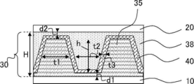
- FIG. 1 is a cross-sectional view (sectional view taken along the line KK ′ of FIG. 2) schematically showing an example of the phosphor-containing film 1 according to the present invention
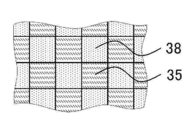
- FIG. 2 is a plan view of FIG.
- FIG. 2 is a perspective view of FIG. 1.
- FIG. 2 only the first fluorescent region and the second fluorescent region in a plan view are shown for explanation, and in FIG. 3, the second base film 20 and the second fluorescent region are not shown. is doing.
- the phosphor-containing film 1 shown in FIG. 1 has a configuration in which a first base film 10, a phosphor-containing layer 30, and a second base film 20 are laminated in this order.
- the phosphor-containing layer 30 has a first fluorescent region 35, a second fluorescent region 38, and a third layer 40 that is stacked between the first fluorescent region 35 and the second fluorescent region 38.
- the first fluorescent region 35 is the first resin layer in the present invention and contains a phosphor.
- the second fluorescent region 38 is the second resin layer in the present invention and contains a phosphor.
- each of the first fluorescent region 35 and the second fluorescent region 38 has an uneven shape on one main surface, and the uneven shape (first unevenness) of the first fluorescent region 35.
- region 38 may fit. That is, in the surface direction (in plan view), the positions of the concave portions of the first fluorescent region 35 and the convex portions of the second fluorescent region 38 coincide with each other, and the convex portions of the first fluorescent region 35 and the second fluorescent region 38 The position of the fluorescent region 38 coincides with the concave portion.
- the third layer follows the fitting portion between the first uneven shape and the second uneven shape between the first fluorescent region 35 and the second fluorescent region 38. It is formed in the shape.
- the third layer is made of an inorganic material and has a gas barrier property.
- the first concavo-convex shape of the first fluorescent region 35 in the plan view of the phosphor-containing film 1 includes a plurality of regular hexagonal concave portions and convex portions, and the closest density. It is the shape arranged by filling. Specifically, a plurality of concave portions and convex portions are formed in a pattern in which six convex portions are arranged around one concave portion. In addition, a groove is formed between adjacent convex portions and is separated from each other. A third layer is also formed in this groove.
- the second uneven shape of the second fluorescent region 38 is a shape in which a plurality of regular hexagonal concave and convex portions are arranged in a close-packed manner, and the first concave and convex shape is a concave and convex portion.
- This is a shape in which the positions of are interchanged. Specifically, a plurality of concave portions and convex portions are formed in a pattern in which six concave portions are arranged around one convex portion.
- the first concavo-convex shape and the second concavo-convex shape having such a shape are laminated so that the positions in the surface direction of one concave portion and the other convex portion coincide with each other. Therefore, as shown in FIG. 2, the first concavo-convex convex portions and the second concavo-convex convex portions are arranged in the closest packing, and a third layer is formed between the convex portions.
- the phosphor-containing film 1 includes a first resin layer having a first concavo-convex shape on one main surface between the first base film 10 and the second base film 20, and 1st unevenness between the 1st resin layer and the 2nd resin layer, the 2nd resin layer which has the 2nd unevenness shape on the principal surface which faces the principal surface which has the 1st unevenness shape of 1 resin layer
- a third layer following the shape and the second concavo-convex shape is included, the first resin layer and the second resin layer include a phosphor, and the third layer is formed of an inorganic material.
- the phosphor region that is, the first phosphor region 35 and the second phosphor region 38 are discretely arranged in the two-dimensional direction through the third layer.
- the fluorescent region other than the fluorescent region that is the cut portion is sealed and surrounded by the third layer, regardless of where the film 1 is cut linearly. Can keep.
- the fluorescent region that is cut and exposed to the outside air loses its original function as a phosphor, but the deactivated fluorescent region becomes a layer that protects the fluorescent region that is not exposed to the outside air from the outside air.
- the depth of the concave portion of the first fluorescent region 35 where the second fluorescent region 38 is arranged is h
- the depth h is It is preferable that they are 1 micrometer or more and 150 micrometers or less.
- the size (width) t1 of the convex portion of the first fluorescent region 35 and the size (width) t2 of the convex portion of the second fluorescent region 38 can be arbitrarily set.
- the size (width) t1 of the convex portion of the fluorescent region 35 is 5 ⁇ m or more and 1000 ⁇ m or less
- the size (width) t2 of the convex portion of the second fluorescent region 38 is 5 ⁇ m or more and 1000 ⁇ m or less.
- the width t1 and the width t2 are widths at a depth position of h / 2, where h is the depth of the concave portion of the first fluorescent region 35.
- a coating process and a curing process are sequentially performed on a long film by a roll-to-roll method.
- a method of cutting to a desired size after forming the laminated structure is preferable.
- the first resin layer having an uneven shape, the second resin layer having an uneven shape, and the third layer following the uneven shape between the first and second resin layers include a phosphor, and the third layer is formed of an inorganic material.
- the phosphor-containing film is cut, it is cut at a portion immediately adjacent to the third layer. Even if the optical component is cut, the area where the fluorescent member is kept sealed can be maximized, and the fluorescent area exposed to the outside air can be minimized. That is, the effective area can be maximized.
- the third layer follows the uneven shape formed by the first resin layer and the second resin layer.
- the third layer that follows the uneven shape seals all or part of the phosphor-containing layer 30 in the thickness direction according to the shape, thereby reducing the amount of oxygen intrusion from the film end and suppressing end deterioration. be able to.
- Clearances d1 and d2 (see FIG. 4) between the third layer and the phosphor-containing layer side surface of the two base films having barrier properties are preferably less than 10 ⁇ m, and more preferably less than 5 ⁇ m. Preferably, it is less than 2 ⁇ m, more preferably less than 0.5 ⁇ m.
- the height (film thickness) H of the phosphor-containing layer 30 can reach the target chromaticity at 1 ⁇ m or more. However, since the influence of the film thickness unevenness on the color becomes large, it is preferable to have a film thickness of a certain level or more. On the other hand, when the film thickness of the fluorescent region is too large, the amount of light absorption increases and the initial luminance may decrease. From these viewpoints, the height H of the phosphor-containing layer 30 is 1 ⁇ m to 150 ⁇ m, preferably 5 ⁇ m to 80 ⁇ m, and more preferably 10 ⁇ m to 50 ⁇ m.
- the width t3 of the third layer is preferably thin from the viewpoint of obtaining a thin phosphor-containing film. On the other hand, a certain width or more is required from the viewpoint of strength and durability. From these viewpoints, the width t3 of the third layer is 0.1 ⁇ m or more and 10 ⁇ m or less, preferably 0.5 ⁇ m or more and 5 ⁇ m or less, and more preferably 0.5 ⁇ m or more and 2 ⁇ m or less.
- the depth h of the concave portion formed in the first fluorescent region is determined by cutting the concave portion of the phosphor-containing film with a microtome to form a cross section and irradiating the phosphor-containing layer with excitation light. Is observed using a confocal laser microscope, 10 recesses are extracted, the depth is measured, and the average value is obtained.
- the width t1 of the convex portion of the first fluorescent region 35 and the width t2 of the convex portion of the second fluorescent region 38 are each excited by forming a cross section by cutting the convex portion of the phosphor-containing film with a microtome.
- this cross section is observed using a confocal laser microscope, ten convex portions are extracted, and the width is measured to obtain an average value.
- the width t3 of the third layer is obtained by cutting the phosphor-containing film with a microtome to form a cross section, observing the cross section with a scanning electron microscope, and obtaining the average value at 10 locations.
- the clearances d1 and d2 between the third layer and the phosphor-containing layer side surface of the two base films having a barrier property are formed by cutting the phosphor-containing film with a microtome and then forming a cross-section. Observed with an electron microscope, the clearance d1 with the first base film is obtained as an average value of 5 places and the clearance d2 with the second base film as a total of 10 places.
- the first fluorescent region 35 is a first resin layer in which the phosphor 31 is dispersed in the binder 33.
- the second fluorescent region 38 is a second resin layer in which the phosphor 36 is dispersed in the binder 39.
- first base film 10 and the second base film 20 are impermeable to oxygen.
- the first base film 10 and the second base film 20 are each a barrier film having a laminated structure of a support film (11, 21) and a barrier layer (12, 22) having an impermeability to oxygen. .
- the size and arrangement pattern of the fluorescent region that is, the first fluorescent region 35 and the second fluorescent region 38 are not particularly limited, and may be appropriately designed according to desired conditions.
- consideration is given to a geometrical constraint for arranging the fluorescent regions apart from each other in plan view, an allowable value of the width of the non-light emitting region generated at the time of cutting, and the like.
- the shortest distance between adjacent fluorescent regions needs to be a distance that can realize an oxygen permeability of the third layer of 10 cc / (m 2 ⁇ day ⁇ atm) or less.
- a desired shape, size, and arrangement pattern may be designed.
- the convex and concave portions of the fluorescent region are regular hexagonal columnar shapes and are regular hexagonal in plan view, but the shape of the fluorescent region is not particularly limited. As shown in FIG. 5, the convex portion and the concave portion may be square in plan view. Alternatively, the convex portion of the fluorescent region may be a polygonal column or a regular polygonal column. Moreover, in the above-mentioned example, although the bottom face of the polygonal column is arrange
- the shape of each fluorescent region may be indefinite. The shape of each fluorescent region may not be the same.
- the area ratio between the first fluorescent region 35 and the second fluorescent region 38 can be freely set.
- the emission wavelengths of the first phosphor included in the first fluorescent region and the second phosphor included in the second fluorescent region 38 are different, it is preferable to adjust the backlight to be white.
- the white point can be adjusted not only by the area ratio of the fluorescent region but also by the concentration of the phosphor in the coating solution.
- the phosphor 31 in the first fluorescent region 35 may be one type or a plurality of types.
- the phosphor 36 in the second fluorescent region 38 may be one type or a plurality of types.
- the first phosphor 31 in the first fluorescence region 35 and the second phosphor 36 in the second fluorescence region 38 have different emission center wavelengths.
- a phosphor having an emission center wavelength in the wavelength band of 520 to 560 nm is used as the first phosphor 31
- a phosphor having an emission center wavelength in the wavelength band of 600 to 680 nm is used as the second phosphor 36. it can.
- the effect of the present invention is remarkably exhibited.
- the effect will be described in detail below.
- the phosphor may be deteriorated due to decomposition of the phosphor itself or desorption of the ligand adsorbed on the phosphor due to heating or the like.
- decomposition products generated during the deterioration of the phosphor and the detached ligand may affect different types of phosphors and promote the deterioration.
- the phosphor When two or more kinds of phosphors having different configurations are used as the phosphor, for example, rare earth doping garnet, silicate, aluminate, phosphate, ceramic phosphor, sulfide phosphor, nitride phosphor, When an inorganic phosphor such as an oxynitride phosphor or a fluoride phosphor and a quantum dot are used in combination, a decomposition product generated when the quantum dot deteriorates or a detached ligand degrades the inorganic phosphor. There is a case. Further, when two types of quantum dots are used as the phosphor, the phosphor may be deteriorated.
- the ligands suitable for each quantum dot are different, there is a case where one of the ligands adsorbs to the other quantum dot to deteriorate the light emission characteristics.
- the detached ligand is adsorbed on each quantum dot and the light emission characteristics are lowered.
- CdSe / ZnS (manufactured by NN-labs, Sigma-Aldrich) is octadecylamine
- CdTe (manufactured by NN-labs) is octadecylphosphonic acid
- InP / ZnS (manufactured by NN-labs).
- the phosphor-containing film 1 includes a first base film 10 and a second base film 20, and has a configuration in which a phosphor-containing layer 30 is sandwiched between two base films 10 and 20.
- the phosphor-containing layer 30 includes a third layer formed of a fluorescent region and an inorganic material, and the fluorescent region includes a first fluorescent region 35 and a second fluorescent region 38.
- the phosphor-containing film of the present invention includes a first fluorescent region 35 and a second fluorescent region 38 as fluorescent regions.
- the first fluorescent region 35 is composed of a phosphor 31 and a binder 33 in which the phosphor 31 is dispersed, and a fluorescent region forming coating solution 32 containing the phosphor 31 and a curable compound is applied. It is formed by curing.
- the second fluorescent region 38 is composed of a fluorescent material 36 and a binder 39 in which the fluorescent material 36 is dispersed, and a fluorescent region forming coating solution 37 containing the fluorescent material 36 and a curable compound is applied, It is formed by curing.
- phosphors can be used as the phosphor that reacts with oxygen and deteriorates when exposed to oxygen.
- phosphors in which semiconductor fine particles are doped with rare earth, and semiconductor nano particles (quantum dots, quantum rods) are also preferably used.
- Phosphors can be used alone, but in order to obtain a desired fluorescence spectrum, a plurality of phosphors having different wavelengths may be used in combination, or a combination of phosphors having different material configurations (for example, A combination of a rare earth-doped garnet and quantum dots may be used.
- being exposed to oxygen means being exposed to an oxygen-containing environment such as the atmosphere, and being deteriorated by reaction with oxygen means that the performance of the phosphor is caused by oxidation of the phosphor.
- the light emission performance is reduced as compared with that before reacting with oxygen.
- the photoelectric conversion efficiency is less than that of oxygen. It means that it is lower than before the reaction.
- a quantum dot is mainly described as an example of a phosphor that deteriorates due to oxygen.
- the phosphor of the present invention is not limited to quantum dots, and other fluorescent dyes that deteriorate due to oxygen, photoelectric conversion materials, and the like.
- the material is not particularly limited as long as it is a material that converts external energy into light or converts light into electricity.
- the phosphor is deteriorated due to decomposition of the phosphor itself or desorption of the ligand adsorbed on the phosphor depending on the structure depending on the structure. There is a case.
- Quantum dot is a fine particle of a compound semiconductor having a size of several nanometers to several tens of nanometers, and at least is excited by incident excitation light to emit fluorescence.
- the phosphor of the present embodiment includes at least one kind of quantum dot and can also include two or more kinds of quantum dots having different emission characteristics.
- Known quantum dots include a quantum dot (A) having an emission center wavelength in a wavelength range of 600 nm to 680 nm, a quantum dot (B) having an emission center wavelength in a wavelength range of 500 nm to less than 600 nm, There is a quantum dot (C) having an emission center wavelength in a wavelength band of 400 nm or more and less than 500 nm.
- the quantum dot (A) is excited by excitation light to emit red light, the quantum dot (B) emits green light, The dot (C) emits blue light.
- red light emitted from the quantum dots (A) and light emitted from the quantum dots (B) are emitted.
- White light can be embodied by green light and blue light transmitted through the phosphor-containing layer.
- ultraviolet light incident on the phosphor-containing layer including the quantum dots (A), (B), and (C) as excitation light, red light emitted from the quantum dots (A), quantum dots (B ) And green light emitted by the quantum dots (C) and white light can be realized.
- quantum dots for example, JP 2012-169271 A paragraphs 0060 to 0066 can be referred to, but are not limited to those described here.
- the quantum dots commercially available products can be used without any limitation.
- the emission wavelength of the quantum dots can usually be adjusted by the composition and size of the particles.
- Quantum dots can be added at, for example, about 0.1 to 10 parts by mass with respect to 100 parts by mass of the total amount of the coating solution.
- Quantum dots may be added in the form of particles in the coating liquid, or may be added in the form of a dispersion dispersed in an organic solvent.
- the addition in the state of a dispersion is preferable from the viewpoint of suppressing the aggregation of the quantum dot particles.
- the organic solvent used for dispersing the quantum dots is not particularly limited.
- quantum dots for example, core-shell type semiconductor nanoparticles are preferable from the viewpoint of improving durability.
- the core II-VI semiconductor nanoparticles, III-V semiconductor nanoparticles, multi-component semiconductor nanoparticles, and the like can be used. Specific examples include CdSe, CdTe, CdS, ZnS, ZnSe, ZnTe, InP, InAs, and InGaP, but are not limited thereto. Among these, CdSe, CdTe, InP, and InGaP are preferable from the viewpoint of emitting visible light with high efficiency.
- the shell CdS, ZnS, ZnO, GaAs, and a composite thereof can be used, but the shell is not limited thereto.
- the emission wavelength of the quantum dots can usually be adjusted by the composition and size of the particles.
- the quantum dots may be spherical particles, may be rod-like particles called quantum rods, and may be tetrapod-type particles. From the viewpoint of narrowing the half width of light emission (full width at half maximum, FWHM) and expanding the color reproduction range of the liquid crystal display device, spherical quantum dots or rod-like quantum dots (that is, quantum rods) are preferable.
- the present invention when two or more types of quantum dots having different configurations or compositions are used, it is preferable to divide them into a first fluorescent region and a second fluorescent region, respectively. Moreover, also when using together 1 or more types of quantum dots, and fluorescent substance other than a quantum dot, it is preferable to divide into a 1st fluorescence area
- the curable compound those having a polymerizable group can be widely employed.
- the kind of polymeric group is not specifically limited, Preferably, it is a (meth) acrylate group, a vinyl group, or an epoxy group, More preferably, it is a (meth) acrylate group, More preferably, it is an acrylate group.
- each polymeric group may be the same and may differ.
- (meth) acrylate compounds such as monofunctional or polyfunctional (meth) acrylate monomers, polymers thereof, prepolymers, and the like are preferable.
- description with "(meth) acrylate” shall be used by the meaning of at least one of an acrylate and a methacrylate, or either. The same applies to “(meth) acryloyl” and the like.
- polymerizable monomer having two polymerizable groups include a bifunctional polymerizable unsaturated monomer having two ethylenically unsaturated bond-containing groups.
- Bifunctional polymerizable unsaturated monomers are suitable for reducing the viscosity of the composition.
- (meth) acrylate compounds that are excellent in reactivity and have no problems such as residual catalyst are preferable.
- the amount of the bifunctional (meth) acrylate monomer used is 5 parts by mass or more from the viewpoint of adjusting the viscosity of the coating liquid to a preferable range with respect to 100 parts by mass of the total amount of the curable compound contained in the coating liquid. It is preferably 10 to 80 parts by mass.
- polymerizable monomer having three or more polymerizable groups examples include polyfunctional polymerizable unsaturated monomers having three or more ethylenically unsaturated bond-containing groups. These polyfunctional polymerizable unsaturated monomers are excellent in terms of imparting mechanical strength. In the present embodiment, (meth) acrylate compounds that are excellent in reactivity and have no problems such as residual catalyst are preferable.
- ECH Epichlorohydrin modified glycerol tri (meth) acrylate
- EO ethylene oxide modified glycerol tri (meth) acrylate
- PO propylene oxide modified glycerol tri (meth) acrylate
- pentaerythritol triacrylate pentaerythritol Tetraacrylate
- EO-modified phosphate triacrylate trimethylolpropane tri (meth) acrylate
- tris (acryloxyethyl) isocyanurate dipentaerythritol hexa (meth) acrylate, dipentaerythritol penta (meth) a Chlorate
- EO-modified glycerol tri (meth) acrylate PO-modified glycerol tri (meth) acrylate, trimethylolpropane tri (meth) acrylate, EO-modified trimethylolpropane tri (meth) acrylate, PO-modified trimethylolpropane tri (Meth) acrylate, dipentaerythritol hexa (meth) acrylate, dipentaerythritol penta (meth) acrylate, pentaerythritol ethoxytetra (meth) acrylate and pentaerythritol tetra (meth) acrylate are preferably used in the present invention.
- the amount of the polyfunctional (meth) acrylate monomer used is 5 parts by mass or more from the viewpoint of the coating strength of the fluorescent-containing layer after curing with respect to 100 parts by mass of the total amount of the curable compound contained in the coating liquid. It is preferable that it is 95 mass parts or less from a viewpoint of gelatinization suppression of a coating liquid.
- Monofunctional- Monofunctional (meth) acrylate monomers include acrylic acid and methacrylic acid, derivatives thereof, and more specifically, monomers having one polymerizable unsaturated bond ((meth) acryloyl group) of (meth) acrylic acid in the molecule Can be mentioned. Specific examples thereof include the following compounds, but the present embodiment is not limited thereto.
- the amount of the monofunctional (meth) acrylate monomer used is 10 parts by mass or more from the viewpoint of adjusting the viscosity of the coating liquid to a preferable range with respect to 100 parts by mass of the total amount of the curable compound contained in the coating liquid. It is preferably 10 to 80 parts by mass.
- -Epoxy compounds, etc.- examples include compounds having a cyclic group such as a cyclic ether group capable of ring-opening polymerization such as an epoxy group and an oxetanyl group. More preferable examples of such a compound include compounds having an epoxy group-containing compound (epoxy compound).
- epoxy compound By using a compound having an epoxy group or an oxetanyl group in combination with a (meth) acrylate compound, the adhesion with the barrier layer tends to be improved.
- Examples of the compound having an epoxy group include polyglycidyl esters of polybasic acids, polyglycidyl ethers of polyhydric alcohols, polyglycidyl ethers of polyoxyalkylene glycols, polyglycidyl ethers of aromatic polyols, and aromatics. Mention may be made, for example, of hydrogenated compounds of polyglycidyl ethers of polyols, urethane polyepoxy compounds and epoxidized polybutadienes. These compounds can be used alone or in combination of two or more thereof.
- the compound having an epoxy group that can be preferably used include, for example, an aliphatic cyclic epoxy compound, bisphenol A diglycidyl ether, bisphenol F diglycidyl ether, bisphenol S diglycidyl ether, brominated bisphenol A diglycidyl ether, Brominated bisphenol F diglycidyl ether, brominated bisphenol S diglycidyl ether, hydrogenated bisphenol A diglycidyl ether, hydrogenated bisphenol F diglycidyl ether, hydrogenated bisphenol S diglycidyl ether, 1,4-butanediol diglycidyl ether, 1,6-hexanediol diglycidyl ether, glycerin triglycidyl ether, trimethylolpropane triglycidyl ether, polyethylene glycol Polyglycidyl ethers of polyether polyols obtained by adding one or more alkylene oxides to aliphatic polyhydric alcohols
- aliphatic cyclic epoxy compounds bisphenol A diglycidyl ether, bisphenol F diglycidyl ether, hydrogenated bisphenol A diglycidyl ether, hydrogenated bisphenol F diglycidyl ether, 1,4-butanediol diglycidyl ether, 1,6-hexanediol diglycidyl ether, glycerin triglycidyl ether, trimethylolpropane triglycidyl ether, neopentyl glycol diglycidyl ether, polyethylene glycol diglycidyl ether, and polypropylene glycol diglycidyl ether are preferred.
- UVR-6216 manufactured by Union Carbide
- glycidol AOEX24
- Cyclomer A200 Celoxide 2021P
- Celoxide 8000 aboveve, Daicel Chemical Industries, Ltd.
- 4-vinylcyclohexene dioxide manufactured by Sigma Aldrich
- Epicoat 828 Epicoat 812
- Epicoat 1031 Epicoat 872
- Epicoat CT508 aboveve, manufactured by Yuka Shell Co., Ltd.
- KRM-2400, KRM-2410, KRM -2408, KRM-2490, KRM-2720, KRM-2750 aboveve, manufactured by Asahi Denka Kogyo Co., Ltd.
- these compounds having an epoxy group or oxetanyl group may be produced by any method.
- Maruzen KK Publishing Co., Ltd., 4th edition Experimental Chemistry Course 20 Organic Synthesis II, 213-, 1992, Ed. By Alfred Hasfner The chemistry OF heterocyclic compounds-Small Ring Heterocycles part3 Oxiranes, John & Wiley and Sons, An Interscience Publication, New York, 1985, Yoshimura, Adhesion, Vol. 29, No. 12, 32, 1985, Yoshimura, Adhesion, Vol. 1986, Yoshimura, Adhesion, Vol. 30, No. 7, 42, 1986, Japanese Patent Application Laid-Open No. 11-1000037, Japanese Patent No. 2906245, Japanese Patent No. 2926262, and the like.
- a vinyl ether compound may be used as the curable compound used in the present embodiment.
- known compounds can be appropriately selected. For example, those described in paragraph No. 0057 of JP-A-2009-73078 can be preferably used.
- vinyl ether compounds are, for example, the method described in Stephen C. Lapin, Polymers Paint Paint, Journal 179 (4237), 321 (1988), that is, the reaction of a polyhydric alcohol or polyhydric phenol with acetylene, or They can be synthesized by the reaction of a polyhydric alcohol or polyhydric phenol and a halogenated alkyl vinyl ether, and these can be used singly or in combination of two or more.
- a silsesquioxane compound having a reactive group described in JP-A-2009-73078 can be used from the viewpoint of reducing the viscosity and increasing the hardness.
- the curable compound that forms the first fluorescent region 35 and the second fluorescent region 38 may be a cationically polymerizable compound or a radically polymerizable compound.
- the polymerizable compound is preferably a radical polymerizable compound
- the photopolymerization initiator is preferably a radical polymerizable curable composition that is a radical polymerization initiator that generates radicals upon light irradiation.
- the curable compound that forms the first fluorescent region 35 and the second fluorescent region 38 may include a silane coupling agent. Since the adhesion with the adjacent third layer and barrier layer is strengthened by the silane coupling agent, even a hydrophobic monomer with poor adhesion can be used in the present invention. This is mainly due to the fact that the silane coupling agent contained in the wavelength conversion layer forms a covalent bond with the surface of the adjacent layer and the constituent components of the layer by hydrolysis reaction or condensation reaction. In addition, when the silane coupling agent has a reactive functional group such as a radical polymerizable group, a monomer component constituting the wavelength conversion layer and a cross-linked structure can also be formed, thereby improving the adhesion between the wavelength conversion layer and the adjacent layer. Can contribute.
- a reactive functional group such as a radical polymerizable group
- silane coupling agent a known silane coupling agent can be used without any limitation.
- a silane coupling agent represented by the general formula (1) described in JP2013-43382A can be exemplified.
- the amount of the additive such as a silane coupling agent is not particularly limited and can be set as appropriate.
- the curable compound that forms the first fluorescent region 35 and the second fluorescent region 38 is not limited to the above-described components, and may be used for other purposes such as an antioxidant within a range that does not impair the effects of the present invention. Ingredients may be included.
- the curable compound that forms the first fluorescent region 35 and the second fluorescent region 38 preferably contains a known antioxidant.
- the content of the antioxidant is, for example, 0.01 to 10% by mass, preferably 0.2 to 5% by mass with respect to the total polymerizable monomer. When using 2 or more types of antioxidant, the total amount becomes the said range.
- the antioxidant suppresses fading caused by heat or light irradiation and fading caused by various oxidizing gases such as ozone, active oxygen, NOx, and SOx (X is an integer).
- oxidizing gases such as ozone, active oxygen, NOx, and SOx
- antioxidants examples include hydrazides, hindered amine antioxidants, nitrogen-containing heterocyclic mercapto compounds, thioether antioxidants, hindered phenol antioxidants, ascorbic acids, zinc sulfate, thiocyanates, Examples include thiourea derivatives, sugars, nitrites, sulfites, thiosulfates, hydroxylamine derivatives, and the like.
- hindered phenol antioxidants and thioether antioxidants are particularly preferable from the viewpoint of preventing coloring of the cured film and reducing the film thickness.
- antioxidants Commercially available products of antioxidants include trade names “Irganox 1010, 1035, 1076, 1222 (above, manufactured by Ciba Geigy Co., Ltd.); ), Trade names ADK STAB AO70, AO80, AO503 (manufactured by ADEKA Corporation) and the like. These may be used alone or in combination.
- the curable compound that forms the first fluorescent region 35 and the second fluorescent region 38 preferably contains a polymerization inhibitor.
- the content of the polymerization inhibitor is 0.001 to 1% by mass, more preferably 0.005 to 0.5% by mass, and still more preferably 0.008 to 0.
- the polymerization inhibitor may be added during production of the polymerizable monomer, or may be added later to the cured composition.
- Preferred polymerization inhibitors include hydroquinone, p-methoxyphenol, di-tert-butyl-p-cresol, pyrogallol, tert-butylcatechol, benzoquinone, 4,4′-thiobis (3-methyl-6-tert-butylphenol) 2,2'-methylenebis (4-methyl-6-tert-butylphenol), N-nitrosophenylhydroxyamine cerium salt, phenothiazine, phenoxazine, 4-methoxynaphthol, 2,2,6,6-tetramethyl Examples include piperidine-1-oxyl free radical, 2,2,6,6-tetramethylpiperidine, 4-hydroxy-2,2,6,6-tetramethylpiperidine-1-oxyl free radical, nitrobenzene, dimethylaniline and the like.
- p-benzoquino 2,2,6,6-tetramethylpiperidine-1-oxyl free radical, 4-hydroxy-2,2,6,6-tetramethylpiperidine-1-oxyl free radical, phenothiazine.
- These polymerization inhibitors suppress the generation of polymer impurities not only during the production of the polymerizable monomer but also during storage of the cured composition, and suppress the deterioration of pattern formation during imprinting.
- the curable compound that forms the first fluorescent region 35 and the second fluorescent region 38 preferably contains inorganic particles.
- the impermeability to oxygen can be increased by containing inorganic particles.
- the inorganic particles include silica particles, alumina particles, zirconium oxide particles, zinc oxide particles, titanium oxide particles, and inorganic layered compounds such as mica and talc.
- the curable compound that forms the first fluorescent region 35 and the second fluorescent region 38 includes a release agent, a silane coupling agent, an ultraviolet absorber, a light stabilizer, and aging as necessary.
- a release agent e.g., a silane coupling agent
- an ultraviolet absorber e.g., a UV absorber
- a light stabilizer e.g., a UV absorber
- aging e.g., UV absorber, a light stabilizer
- the third layer is made of an inorganic material and has a function of suppressing oxygen permeation.
- an inorganic material which comprises a 3rd layer there is no limitation in particular as an inorganic material which comprises a 3rd layer,
- various inorganic compounds such as a metal or an inorganic oxide, nitride, oxynitride, can be used.
- silicon, aluminum, magnesium, titanium, tin, indium and cerium are preferable, and one or two or more of these may be included.
- Specific examples of the inorganic compound include silicon oxide, silicon oxynitride, aluminum oxide, magnesium oxide, titanium oxide, tin oxide, indium oxide alloy, silicon nitride, aluminum nitride, and titanium nitride.
- a metal film such as an aluminum film, a silver film, a tin film, a chromium film, a nickel film, or a titanium film may be provided.
- a glass layer from an organosilane compound by a sol-gel method.
- the third layer can be obtained in a shape that follows the irregularities without any defects.
- the organosilane compound polysilazane or an alkoxysilane compound represented by the following formula (1) is preferable.
- polysilazane is more preferable because an organic component does not remain after conversion to SiO 2 , and high barrier properties are easily obtained.
- the polysilazane As the polysilazane, a commercially available product prepared by adding a catalyst is available, and the Aquamica series (manufactured by AZ Electronic Materials) can be used as it is or diluted with a solvent.
- the Aquamica series manufactured by AZ Electronic Materials
- NP110, NP140, SP140, and UP140 that convert to SiO 2 at a low temperature are more preferable.
- trialkoxysilanes such as trimethoxysilane, triethoxysilane, and tripropoxysilane
- monomethyltrimethoxysilane monomethyltriethoxysilane, monomethyltripropoxys
- Monoalkyldialkoxysilanes such as diethoxysilane, monoethyldipropoxysilane, monopropyldimethoxysilane, monopropyldiethoxysilane, monopropyldipropoxysilane; dimethyldimethoxysilane, dimethyldiethoxysilane, dimethyldipropoxysilane, diethyldimethoxy Silane, diethyldiethoxysilane, diethyldipropoxysilane, dipropyldimethoxysilane, dipropyldiethoxysilane, dipropyldipropoxysilane Dialkyl dialkoxy silane; diphenyldimethoxysilane, such as diphenyl dialkoxysilane such as diphenyl diethoxy silane.
- the third layer preferably has an oxygen permeability of 10 cc / (m 2 ⁇ day ⁇ atm) or less at the shortest distance between the adjacent first fluorescent region 35 and second fluorescent region 38.
- the oxygen permeability at the shortest distance between the first fluorescent region 35 and the second fluorescent region 38 adjacent to each other in the third layer is more preferably 1 cc / (m 2 ⁇ day ⁇ atm) or less, and 10 ⁇ 1 cc. / (M 2 ⁇ day ⁇ atm) or less is more preferable.
- the required minimum distance differs depending on the composition of the third layer.
- the minimum required distance between the first fluorescent region 35 and the second fluorescent region 38 differs depending on the composition of the third layer, but as an example, the minimum distance between adjacent fluorescent regions 35 in the third layer, that is, the first
- the width of the three layers is preferably 0.001 mm to 3 mm, more preferably 0.01 mm to 2 mm, and particularly preferably 0.03 mm to 2 mm. If the width of the third layer is too short, it is difficult to ensure the required oxygen permeability, and if the width of the third layer is too wide, luminance unevenness of the display device is deteriorated, which is not preferable.
- the base films 10 and 20 are preferably films having a function of suppressing oxygen permeation.
- the base films 10 and 20 have the structure which respectively provided the barrier layers 12 and 22 on the one surface of the support films 11 and 21, respectively.
- the presence of the support films 11 and 21 improves the strength of the phosphor-containing film, and enables easy film formation.
- Each of the base films 10 and 20 preferably has a total light transmittance of 80% or more in the visible light region, and more preferably 85% or more.
- the visible light region refers to a wavelength region of 380 to 780 nm, and the total light transmittance indicates an average value of light transmittance over the visible light region.
- Each of the base films 10 and 20 preferably has an oxygen permeability of 1.00 cc / (m 2 ⁇ day ⁇ atm) or less.
- the oxygen permeability is more preferably 0.1 cc / (m 2 ⁇ day ⁇ atm) or less, further preferably 0.01 cc / (m 2 ⁇ day ⁇ atm) or less, and particularly preferably 0.001 cc / (M 2 ⁇ day ⁇ atm) or less.
- the oxygen permeability is a value measured using an oxygen gas permeability measuring apparatus (manufactured by MOCON, OX-TRAN 2/20: trade name) under the conditions of a measurement temperature of 23 ° C. and a relative humidity of 90%. is there.
- the base films 10 and 20 preferably have a function of blocking moisture (water vapor) in addition to a gas barrier function of blocking oxygen.
- the moisture permeability (water vapor permeability) of the base films 10 and 20 is preferably 0.10 g / (m 2 ⁇ day ⁇ atm) or less, preferably 0.01 g / (m 2 ⁇ day ⁇ atm) or less. Is more preferable.
- a flexible belt-like support that is transparent to visible light is preferable.
- transparent to visible light means that the linear transmittance in the visible light region is 80% or more, preferably 85% or more.
- the light transmittance used as a measure of transparency is measured by measuring the total light transmittance and the amount of scattered light using the method described in JIS-K7105, that is, using an integrating sphere light transmittance measuring device. It can be calculated by subtracting the rate.
- the support film preferably has a barrier property against oxygen and moisture.
- Preferred examples of the support film include a polyethylene terephthalate film, a film made of a polymer having a cyclic olefin structure, and a polystyrene film.
- the thickness of the support film is within the range of 10 to 500 ⁇ m, particularly within the range of 15 to 300 ⁇ m, particularly within the range of 15 to 120 ⁇ m, more particularly within the range of 15 to 100 ⁇ m, from the viewpoints of gas barrier properties, impact resistance, etc. Furthermore, it is preferably 25 to 110 ⁇ m, more preferably 25 to 60 ⁇ m.
- the barrier layers 12 and 22 are layers that mainly exhibit gas barrier properties.
- the barrier layers 12 and 22 may include at least one inorganic layer and at least one organic layer. Laminating a plurality of layers in this manner is preferable from the viewpoint of improving light resistance because the barrier property can be further enhanced.
- the number of layers to be stacked increases, the light transmittance of the base film tends to decrease. Therefore, it is desirable to increase the number of layers within a range in which good light transmittance can be maintained.
- the barrier layers 12 and 22 preferably have a total light transmittance in the visible light region of 80% or more and an oxygen permeability of 1.00 cc / (m 2 ⁇ day ⁇ atm) or less. It is preferable.
- the oxygen permeability of the barrier layers 12 and 22 is more preferably 0.1 cc / (m 2 ⁇ day ⁇ atm) or less, particularly preferably 0.01 cc / (m 2 ⁇ day ⁇ atm) or less, and particularly preferably. Is 0.001 cc / (m 2 ⁇ day ⁇ atm) or less. The lower the oxygen permeability, the better, and the higher the total light transmittance in the visible light region, the better.
- the inorganic layer in the barrier layers 12 and 22 is a layer mainly composed of an inorganic material, preferably a layer formed only from an inorganic material.
- the inorganic layer in the barrier layer is preferably a layer having a gas barrier function of blocking oxygen.
- the oxygen permeability of the inorganic layer is preferably 1.00 cc / (m 2 ⁇ day ⁇ atm) or less.
- the oxygen permeability of the inorganic layer can be obtained by attaching a wavelength conversion layer to the detection part of an oxygen meter made by Orbis Fair Laboratories via silicon grease and converting the oxygen permeability from the equilibrium oxygen concentration value. It is also preferable that the inorganic layer has a function of blocking water vapor.
- inorganic layers in the barrier layer may be included in the barrier layer.
- the thickness of the inorganic layer in the base film may be 1 to 500 nm, preferably 5 to 300 nm, and particularly preferably 10 to 150 nm. This is because when the film thickness of the inorganic layer is within the above-described range, it is possible to suppress reflection in the inorganic layer while providing good barrier properties, and to provide a laminated film with higher light transmittance. .
- the inorganic material constituting the inorganic layer in the barrier layer is not particularly limited, and for example, various inorganic compounds such as metals or inorganic oxides, nitrides, oxynitrides, and the like can be used.
- silicon, aluminum, magnesium, titanium, tin, indium and cerium are preferable, and one or two or more of these may be included.
- Specific examples of the inorganic compound include silicon oxide, silicon oxynitride, aluminum oxide, magnesium oxide, titanium oxide, tin oxide, indium oxide alloy, silicon nitride, aluminum nitride, and titanium nitride.
- a metal film such as an aluminum film, a silver film, a tin film, a chromium film, a nickel film, or a titanium film may be provided.
- the inorganic layer having the barrier property is particularly preferably an inorganic layer containing at least one compound selected from silicon nitride, silicon oxynitride, silicon oxide, and aluminum oxide. Since the inorganic layer made of these materials has good adhesion to the organic layer, even when the inorganic layer has pinholes, the organic layer can effectively fill the pinholes and suppress breakage. In addition, it is possible to form an extremely excellent inorganic layer film even in a case where an inorganic layer is further laminated, and to further increase the barrier property.
- the organic layer in the barrier layer is a layer mainly composed of an organic material, and preferably refers to a layer in which the organic material occupies 50% by mass or more, more preferably 80% by mass or more, and particularly 90% by mass or more. .
- JP, 2007-290369, A paragraphs 0020-0042 and JP, 2005-096108, A paragraphs 0074-0105 can be referred to as an organic layer in a barrier layer.
- an organic layer contains a cardo polymer within the range which satisfies said adhesive force conditions. Thereby, the adhesiveness between the organic layer and the adjacent layer, particularly the adhesiveness with the inorganic layer is improved, and a further excellent gas barrier property can be realized.
- the cardo polymer reference can be made to paragraphs 0085 to 0095 of JP-A-2005-096108 described above.
- the thickness of the organic layer is preferably in the range of 0.05 to 10 ⁇ m, and more preferably in the range of 0.5 to 10 ⁇ m.
- the thickness of the organic layer is preferably in the range of 0.5 to 10 ⁇ m, and more preferably in the range of 1 to 5 ⁇ m.
- it is preferably in the range of 0.05 to 5 ⁇ m, more preferably in the range of 0.05 to 1 ⁇ m. This is because when the film thickness of the organic layer formed by the wet coating method or the dry coating method is within the above-described range, the adhesion with the inorganic layer can be further improved.
- the base film can include a light scattering layer.
- the light scattering layer is preferably provided on the surface of the base film that does not contact the phosphor-containing layer 30 of the support film.
- the haze of the phosphor-containing film can be increased, and the emission of the phosphor can be efficiently taken out. Therefore, when a phosphor-containing film is incorporated in a backlight as a wavelength conversion member, a backlight with high luminance can be obtained.
- the thickness of the light scattering layer is preferably in the range of 1 to 15 ⁇ m, more preferably in the range of 1 to 10 ⁇ m, and even more preferably in the range of 1 to 15 ⁇ m from the viewpoint of achieving both light scattering properties and thinning of the light scattering layer.
- the range is 6 ⁇ m.
- the light scattering layer is formed by, for example, applying the polymerizable composition on a suitable substrate, drying the solvent as necessary to remove the solvent, and then polymerizing and curing by light irradiation, heating, or the like. Can do.
- a substrate on which a wavelength conversion layer has already been formed, or a substrate on which a wavelength conversion layer is formed after the light scattering layer is formed can be used as the substrate.
- a wavelength conversion member having a wavelength conversion layer and a light scattering layer can be obtained via the substrate or on the substrate.
- various well-known coating methods mentioned later regarding formation of a wavelength conversion layer are mentioned.
- the curing conditions can be appropriately set according to the type of polymerizable compound used and the composition of the polymerizable composition.
- the light scattering layer is a layer containing light scattering particles in a matrix.
- the particle size of the light scattering particles is 0.1 ⁇ m or more, and is preferably in the range of 0.5 to 15.0 ⁇ m, more preferably in the range of 0.7 to 12.0 ⁇ m from the viewpoint of the scattering effect. preferable. Further, in order to further improve the luminance and adjust the luminance distribution with respect to the viewing angle, two or more kinds of light scattering particles having different particle sizes may be mixed and used.
- the large particle size imparts external scattering properties and anti-Newton ring properties.
- the particle size is preferably in the range of 5.0 ⁇ m to 15.0 ⁇ m, and more preferably in the range of 6.0 ⁇ m to 12.0 ⁇ m.
- the small particle size is preferably in the range of 0.5 ⁇ m to 5.0 ⁇ m, more preferably in the range of 0.7 ⁇ m to 3.0 ⁇ m, from the viewpoint of imparting internal scattering properties. .
- the light scattering particles may be organic particles, inorganic particles, or organic-inorganic composite particles.
- synthetic resin particles can be used as the organic particles.
- Specific examples include silicone resin particles, acrylic resin particles (polymethyl methacrylate (PMMA)), nylon resin particles, styrene resin particles, polyethylene particles, urethane resin particles, benzoguanamine particles, and the like, and particles having a suitable refractive index. From the viewpoint of availability, silicone resin particles and acrylic resin particles are preferable. Also, particles having a hollow structure can be used.
- the refractive index difference ⁇ n between the light scattering particles and the matrix is preferably 0.02 or more, more preferably 0.10 or more, and further preferably 0.20 or more.
- the refractive index of the light scattering particles is, for example, in the range of 1.40 to 1.45, and preferably in the range of 1.42 to 1.45.
- the refractive index here also refers to the above-mentioned average refractive index. The same applies to the “refractive index” described below.
- the light scattering particles are preferably contained in the light scattering layer in a volume fraction of 10 volume% (vol%) to 70 vol%, and 20 vol. More preferably, it is contained in an amount of from 60% to 60% by volume.
- a light-scattering layer As a viewpoint of productivity, etc., forming a light-scattering layer as a cured layer of a polymerizable composition (curable composition) containing light-scattering particles and a polymerizable compound Is preferred.
- a polymerizable composition curable composition
- an appropriate polymerizable compound is selected from commercially available products or those synthesized by a known method in consideration of the refractive index of the material forming the wavelength conversion layer so as to satisfy n1 ⁇ n2. That's fine.
- Preferred polymerizable compounds include, for example, compounds having an ethylenically unsaturated bond in at least one of the terminal and side chains and / or compounds having an epoxy group or oxetane group in at least one of the terminal and side chains.
- a compound having an ethylenically unsaturated bond in at least one of a terminal and a side chain is more preferable.
- Specific examples of the compound having an ethylenically unsaturated bond at at least one of the terminal and the side chain include (meth) acrylate compounds, acrylamide compounds, styrene compounds, maleic anhydride, etc., and (meth) acrylate compounds. Compounds are preferred, and acrylate compounds are more preferred.
- (meth) acrylate compound As the (meth) acrylate compound, (meth) acrylate, urethane (meth) acrylate, polyester (meth) acrylate, epoxy (meth) acrylate and the like are preferable.
- styrene compound styrene, ⁇ -methylstyrene, 4-methylstyrene, divinylbenzene, 4-hydroxystyrene, 4-carboxystyrene and the like are preferable. It is also preferable to use a compound having a fluorene skeleton as the acrylate compound. Specific examples of such compounds include compounds represented by formula (2) described in WO2013 / 047524A1.
- the refractive index adjusting particles are less than 0.1 ⁇ m.
- the refractive index adjusting particles include particles of diamond, titanium oxide, zirconium oxide, lead oxide, lead carbonate, zinc oxide, zinc sulfide, antimony oxide, silicon oxide, aluminum oxide, and the like.
- zirconium oxide and silicon oxide particles are preferable from the viewpoint of little absorption of blue light and ultraviolet light, and zirconium oxide particles are preferable because the refractive index can be adjusted with a small amount.
- the refractive index adjusting particles may be used in an amount capable of adjusting the refractive index, and the content in the light scattering layer is not particularly limited.
- the polymerizable composition for forming the light scattering layer one or more kinds of known additives such as a polymerization initiator and a surfactant, or one or more kinds of solvents for adjusting the viscosity, etc., in an arbitrary amount. It can also be added.
- known additives such as a polymerization initiator and a surfactant, or one or more kinds of solvents for adjusting the viscosity, etc.
- solvents for adjusting the viscosity, etc.
- a first fluorescent region forming coating liquid containing quantum dots (or quantum rods) as a phosphor is prepared. Specifically, components such as quantum dots, curable compounds, thixotropic agents, polymerization initiators, and silane coupling agents dispersed in an organic solvent are mixed in a tank or the like to form a first fluorescent region.
- a coating solution 32 is prepared.
- the fluorescent region forming coating solution may not contain an organic solvent.
- the second fluorescent region forming coating solution 37 is prepared in the same procedure as in the first coating solution preparation step.
- a coating solution containing an inorganic material is prepared.
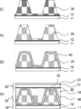
- First fluorescent region forming step Next, a predetermined pattern printing is performed on the barrier layer 12 of the first base film 10 using the first fluorescent region forming coating solution 32 (S1), and if necessary, the solvent is evaporated to obtain the first fluorescent light.
- the region forming coating liquid 32 is cured to form the first fluorescent region 35 (S2).
- the third layer coating solution 37 is applied to the surface of the first fluorescent region 35 and cured (S3). Thereby, the third layer 40 having an impermeability to oxygen is formed.
- a second fluorescent region forming coating solution 37 is applied and filled on the third layer of the concave portion of the first fluorescent region 35.
- the coating film coated with the coating solution 37 that is wound around the backup roller and transported, and wrapped around the laminating roller and transported.
- the second base film is sandwiched between a pasting roller and a backup roller and nipped, thereby pasting (laminating) the second base film on the coating surface side of the coating film.
- the phosphor-containing film of the embodiment can be manufactured by performing the combining step and then curing the coating liquid 37 (S4).
- the phosphor-containing film 1 of the embodiment can be manufactured through the above steps. Note that the first fluorescent region forming step and the second fluorescent region forming step may be performed in reverse order.
- a continuous (long) phosphor-containing film can be obtained by performing the above steps in a roll-to-roll apparatus.
- the obtained phosphor-containing film is cut (cut) by a cutting machine if necessary.
- corrugated pattern in a 1st fluorescence region formation process is demonstrated.
- a step of applying the first fluorescent region forming coating liquid 32 on the base film, a step of pressing the mold against the surface of the coating layer, a step of irradiating the coating film with light A so-called optical imprint method in which a fine uneven pattern is formed through a peeling step can be used.
- the first fluorescent region forming coating solution 32 may be poured between the base film and the mold, and may be photo-cured while pressing the mold. Furthermore, after light irradiation, it may be further heated and cured.
- Such optical imprint lithography can be laminated and multiple patterned, and can be used in combination with thermal imprint.
- pattern formation can also be performed by an inkjet method or a dispenser method.
- the 1st fluorescent region formation coating liquid 32 is apply
- a method of applying the coating liquid 32 on the substrate generally known application methods such as dip coating, air knife coating, curtain coating, wire bar coating, gravure coating, and extrusion coating are used.
- a spin coating method, a slit scanning method, a casting method, an ink jet method, or the like a coating film or droplets can be applied on the base film.
- the first fluorescent region forming coating solution 32 is suitable for a gravure coating method and a casting method.
- the film thickness of the pattern forming layer (coating layer for forming a pattern) composed of the coating film of the coating liquid 32 is about 1 to 150 ⁇ m, although it varies depending on the intended use.
- the coating liquid 32 may be applied by multiple coating.
- you may form other organic layers, such as a planarization layer, between a base film and a pattern formation layer, for example. Thereby, since a pattern formation layer and a base film do not contact directly, adhesion of the dust with respect to a base film, damage to a base film, etc. can be prevented.
- a mold is pressed against the surface of the pattern forming layer.
- a curable compound may be applied to a mold having a pattern and the substrate may be pressed.
- a light transmissive material is selected for at least one of the molding material and / or the base material.
- a curable compound is applied onto a substrate to form a pattern forming layer, a light-transmitting mold is pressed against the surface of the pattern forming layer, and light is irradiated from the back surface of the mold. Curing the curable compound.
- a curable compound can be applied on a light-transmitting substrate, a mold can be pressed against the surface of the coating layer, and light can be irradiated from the back surface of the substrate to cure the curable compound.
- the light irradiation may be performed with the mold attached or after the mold is peeled off, but is preferably performed with the mold in close contact.
- a mold having a pattern to be transferred is used as the mold.
- the pattern on the mold can be formed according to desired processing accuracy by, for example, photolithography, electron beam drawing, or the like, but the mold pattern forming method is not particularly limited.
- the light-transmitting mold material is not particularly limited as long as it has predetermined strength and durability. Specifically, a light transparent resin such as glass, quartz, PMMA, and polycarbonate resin, a transparent metal vapor-deposited film, a flexible film such as polydimethylsiloxane, a photocured film, and a metal film such as SUS are exemplified.
- the non-light-transmitting mold material is not particularly limited as long as it has a predetermined strength.
- Specific examples include ceramic materials, vapor deposition films, magnetic films, reflective films, metal substrates such as Ni, Cu, Cr, and Fe, and substrates such as SiC, silicon, silicon nitride, polysilicon, silicon oxide, and amorphous silicon. Is done.
- the shape of the mold is not particularly limited, and may be either a plate mold or a roll mold. The roll mold is applied particularly when continuous transfer productivity is required.
- the mold may be a mold that has been subjected to a release treatment in order to improve the peelability between the pattern forming layer and the mold surface.
- a release treatment in order to improve the peelability between the pattern forming layer and the mold surface.
- examples of such molds include those that have been treated with a silicon-based or fluorine-based silane coupling agent, such as OPTOOL DSX manufactured by Daikin Industries, Ltd., Novec EGC-1720 manufactured by Sumitomo 3M Co., Ltd. Commercially available release agents can also be suitably used.
- the mold pressure it is usually preferable to perform the mold pressure at 10 atm or less.
- the mold pressure it is preferable to select a region in which uniformity of mold transfer can be ensured within a range in which the remaining film of the pattern forming layer on the mold convex portion is reduced.
- the irradiation amount of light irradiation in the step of irradiating the pattern forming layer with light may be sufficiently larger than the irradiation amount necessary for curing.
- the irradiation amount necessary for curing is appropriately determined by examining the consumption of unsaturated bonds of the curable composition and the tackiness of the cured film.
- the substrate temperature during light irradiation is usually room temperature, but light irradiation may be performed while heating in order to increase the reactivity.
- a preferable degree of vacuum at the time of light irradiation is in the range of 10 ⁇ 1 Pa to 1 atm.
- the light used for curing the pattern forming layer is not particularly limited, and examples thereof include high-energy ionizing radiation, light having a wavelength in the region of near ultraviolet, far ultraviolet, visible, infrared, or radiation.
- high-energy ionizing radiation source for example, an electron beam accelerated by an accelerator such as a cockcroft accelerator, a handagraaf accelerator, a linear accelerator, a betatron, or a cyclotron is industrially most conveniently and economically used.
- an accelerator such as a cockcroft accelerator, a handagraaf accelerator, a linear accelerator, a betatron, or a cyclotron
- radiation such as ⁇ rays, X rays, ⁇ rays, neutron rays, proton rays emitted from radioisotopes or nuclear reactors can also be used.
- the ultraviolet ray source examples include an ultraviolet fluorescent lamp, a low-pressure mercury lamp, a high-pressure mercury lamp, an ultrahigh-pressure mercury lamp, a xenon lamp, a carbon arc lamp, a solar lamp, and an LED (light-emitting diode).
- the radiation includes, for example, microwaves and EUV (extreme ultraviolet).
- laser light used in semiconductor microfabrication such as LED, semiconductor laser light, or 248 nm KrF excimer laser light or 193 nm ArF excimer laser can be suitably used in the present invention. These lights may be monochromatic lights, or may be lights having different wavelengths (mixed lights).
- the exposure illuminance is preferably in the range of 1 mW / cm 2 to 50 mW / cm 2 .
- the exposure dose is preferably in the range of 5 mJ / cm 2 to 1000 mJ / cm 2 . If it is less than 5 mJ / cm 2 , the exposure margin becomes narrow, photocuring becomes insufficient, and problems such as adhesion of unreacted substances to the mold tend to occur.
- the permanent film may be deteriorated due to decomposition of the composition.
- an inert gas such as nitrogen or argon may be flowed to control the oxygen concentration to less than 100 mg / L.
- the pattern formation method may include a step of further curing by applying heat to the cured pattern as necessary after curing the pattern formation layer by light irradiation.
- the heat for heat-curing the composition of the present invention after light irradiation is preferably 150 to 280 ° C, more preferably 200 to 250 ° C.
- the time for applying heat is preferably 5 to 60 minutes, more preferably 15 to 45 minutes.
- the pattern to be formed can take any form, and examples thereof include a lattice mesh pattern in which concave or convex portions are regular tetragons, and a honeycomb pattern in which concave or convex portions are regular hexagons.
- a honeycomb pattern having a regular hexagonal concave portion or convex portion is particularly preferable from the viewpoint of effectively blocking oxygen to the phosphor layer with respect to any cutting form of the present invention.
- FIG. 7 is a schematic diagram showing a side-edge type backlight as an example of a schematic configuration of the backlight unit.
- the backlight unit 102 has a planar shape including a light source 101A that emits primary light (blue light LB) and a light guide plate 101B that guides and emits primary light emitted from the light source 101A.
- the retroreflective member 102B is provided.
- the reflecting plate 102A, the light guide plate 101B, the wavelength conversion member 100, and the retroreflective member 102B are shown separated from each other, but this indicates that they are not optically in close contact. May be laminated.
- the wavelength conversion member 100 emits fluorescence using at least a part of the primary light LB emitted from the planar light source 101C as excitation light, secondary light (green light LG, red light LR) composed of this fluorescence, and wavelength conversion.
- the primary light LB transmitted through the member 100 is emitted.
- a phosphor-containing layer including quantum dots that emit green light LG and quantum dots that emit red light LR by irradiation with blue light LB is sandwiched between first and second base films. It is the fluorescent substance containing film formed by being made.
- LB, LG, and LR emitted from the wavelength conversion member 100 are incident on the retroreflective member 102B, and each incident light is repeatedly reflected between the retroreflective member 102B and the reflecting plate 102A. , It passes through the wavelength conversion member 100 many times. As a result, a sufficient amount of excitation light (blue light LB) is absorbed by the phosphor 31 (here, quantum dots) in the phosphor-containing layer 30 in the wavelength conversion member 100, and a necessary amount of fluorescence (LG, LR). ), And the white light LW is embodied and emitted from the retroreflective member 102B.
- a backlight unit that is a multi-wavelength light source.
- blue light having an emission center wavelength in a wavelength band of 430 to 480 nm and a peak of emission intensity having a half width of 100 nm or less, and an emission center wavelength in a wavelength band of 500 to 600 nm and having a half width of It is preferable to emit green light having an emission intensity peak of 100 nm or less and red light having an emission center wavelength in a wavelength band of 600 nm to 680 nm and a emission intensity peak having a half width of 100 nm or less.
- the wavelength band of blue light emitted from the backlight unit is more preferably 440 nm to 460 nm.
- the wavelength band of the green light emitted from the backlight unit is preferably 520 nm to 560 nm, and more preferably 520 nm to 545 nm.
- the wavelength band of red light emitted from the backlight unit is more preferably 610 nm to 650 nm.
- the half-value widths of the emission intensity of blue light, green light, and red light emitted from the backlight unit are all preferably 80 nm or less, more preferably 50 nm or less, and 40 nm or less. More preferably, it is more preferably 30 nm or less. Among these, it is particularly preferable that the half-value width of each emission intensity of blue light is 25 nm or less.
- the light source 101A is a blue light emitting diode that emits blue light having a light emission center wavelength in a wavelength band of 430 nm to 480 nm, for example, but an ultraviolet light emitting diode that emits ultraviolet light may be used.
- a laser light source other than a light emitting diode can be used.
- a phosphor that emits blue light when irradiated with ultraviolet light, a phosphor that emits green light, and A phosphor that emits red light may be included.
- FIG. 7 illustrates the edge light method using a light guide plate, a reflection plate, or the like as a constituent member.
- the backlight unit is a direct type with a plurality of light sources arranged on the reflection plate and provided with a diffusion plate. It does not matter. Any known light guide plate or diffuser plate can be used without any limitation.
- the retroreflective member 102B may be configured by a known diffusion plate, diffusion sheet, prism sheet (for example, BEF series manufactured by Sumitomo 3M), a light guide, or the like.
- the configuration of the retroreflective member 102B is described in Japanese Patent No. 3416302, Japanese Patent No. 3363565, Japanese Patent No. 4091978, Japanese Patent No. 3448626, and the contents of these publications are incorporated in the present invention.
- the backlight unit of the present invention can be suitably used as a backlight for a liquid crystal display device.
- Example 1 (Preparation of base film 10) A polyethylene terephthalate (PET) film (trade name “Cosmo Shine (registered trademark) A4300”, thickness 50 ⁇ m, manufactured by Toyobo Co., Ltd.) is used as the support film 11, and an organic layer and an inorganic layer are formed on one side of the support by the following procedure. Were sequentially formed.
- PET polyethylene terephthalate
- an inorganic layer (silicon nitride layer) was formed on the surface of the organic layer using a roll-to-roll CVD apparatus.
- Silane gas (flow rate 160 sccm), ammonia gas (flow rate 370 sccm), hydrogen gas (flow rate 590 sccm), and nitrogen gas (flow rate 240 sccm) were used as source gases.
- a high frequency power supply having a frequency of 13.56 MHz was used as the power supply.
- the film forming pressure was 40 Pa, and the reached film thickness was 50 nm.
- an acrylate compound (Viscoat 700HV manufactured by Osaka Organic Synthesis Co., Ltd.) and 40 g of an acrylate compound (8BR500 manufactured by Taisei Fine Chemical Co., Ltd.) were added and further stirred.
- a photopolymerization initiator (Irgacure (registered trademark) 819 manufactured by BASF) and 0.5 g of a fluorosurfactant (FC4430 manufactured by 3M) were further added to form a coating solution (polymerizable composition for forming a light scattering layer). ) was produced.
- the feeding was set so that the PET film surface of the substrate film 10 was a coating surface, and the substrate film 10 was transported to a die coater for coating.
- the wet coating amount was adjusted with a liquid feed pump, and coating was performed at a coating amount of 25 cc / m 2 (the thickness was adjusted to be about 12 ⁇ m with a dry film).
- a base film with a light scattering layer was obtained as a laminated film of the base film 10 and the light scattering layer.
- the following polymerizable composition 1 was prepared, filtered through a polypropylene filter having a pore size of 0.2 ⁇ m, and then dried under reduced pressure for 30 minutes to obtain a first fluorescent region forming coating solution.
- the following polymerizable composition 2 was prepared, filtered through a polypropylene filter having a pore size of 0.2 ⁇ m, and then dried under reduced pressure for 30 minutes to obtain a second fluorescent region forming coating solution.
- Aquamica NP140 manufactured by AZ Electronic Materials
- Quantum dot 2 in toluene dispersion 2 parts by mass Dicyclopentanyl acrylate (FA-513AS (manufactured by Hitachi Chemical Co., Ltd.)) 78.4 parts by mass Tricyclodecane dimethanol diacrylate (A-DCP (manufactured by Shin-Nakamura Chemical Co., Ltd.)) 20 0.0 part by mass Photopolymerization initiator (Irgacure TPO (manufactured by BASF Corporation)) 0.2 parts by mass Silane coupling agent (KBM-5103 (manufactured by Shin-Etsu Chemical Co., Ltd.)) 2.0 parts by mass of antioxidant (trioctyl phosphite (manufactured by Tokyo Chemical Industry Co., Ltd.)) 0.4 mass part
- Quantum dot 1 (CZ520-100, manufactured by NN-Labs) is a core / shell type quantum dot in which the core is made of CdSe and the shell is made of ZnS, the emission center wavelength is 520 nm, and the half width is 30 nm. .
- Octadecylamine is coordinated to the quantum dot 1 as a ligand.
- Quantum dot 2 (INP620-100, manufactured by NN-Labs) is a core / shell type quantum dot in which the core is made of InP and the shell is made of ZnS, the emission center wavelength is 620 nm, and the half width is 40 nm. It is.
- As a ligand, oleylamine and a phosphine derivative are coordinated to the quantum dot 2.
- the first fluorescent region forming coating solution is applied onto the first base film 10 and transferred to the concave portions, followed by photocuring to have a plurality of concave portions.
- a first fluorescent region was formed.
- the recesses were in a square shape of 250 ⁇ m ⁇ 250 ⁇ m, a lattice pattern, the depth of the recesses was 40 ⁇ m, and the width was 50 ⁇ m.
- a 160 W / cm air-cooled metal halide lamp manufactured by Eye Graphics Co., Ltd. was used to cure the resin layer by irradiating ultraviolet rays from the first film side at 2000 mJ / cm 2 .
- the third layer coating solution is applied on the first fluorescent region with a die coater to form a coating film having a thickness of 50 ⁇ m, and then dried and cured by passing through a heating zone at 100 ° C. for 3 minutes.
- a third layer was formed to a thickness of 1 ⁇ m.
- a second fluorescent region forming coating solution is applied on the first base film on which the first fluorescent region and the third layer having a plurality of recesses are formed. After coating and filling the recess with the second fluorescent region forming coating liquid, and pasting the base film with a light scattering layer as the second base film, the second fluorescent region forming coating liquid is photocured.
- a phosphor-containing film was prepared by forming a first fluorescent region having an uneven shape, a second fluorescent region having an uneven shape, and a phosphor-containing layer having a third layer.
- a 160 W / cm air-cooled metal halide lamp manufactured by Eye Graphics Co., Ltd. was used to cure the fluorescent region by irradiating 2000 mJ / cm 2 with ultraviolet rays from the first base film side. Heated at 0 ° C. for 10 minutes. The thickness of the phosphor-containing layer of the obtained phosphor-containing film was 40 ⁇ m.
- t1 was 400 ⁇ m
- t2 was 400 ⁇ m
- t3 was 1 ⁇ m
- d1 and d2 were 0.5 ⁇ m
- h was 37 ⁇ m
- H was 40 ⁇ m.
- Example 2 A phosphor-containing film is produced in the same manner as in Example 1 except that the phosphor contained in the first fluorescent region forming coating solution and the second fluorescent region forming coating solution is a mixture of quantum dots 1 and 2. did.
- a commercially available tablet terminal (trade name “Kindle (registered trademark) Fire HDX 7”, manufactured by Amazon, Inc., hereinafter simply referred to as “Kindle Fire HDX 7”) may be disassembled and back mounted. The light unit was taken out. Instead of QDEF (Quantum Dot Enhancement Film), the phosphor-containing film of Example or Comparative Example cut into a rectangle was incorporated. In this way, a liquid crystal display device was produced. The prepared liquid crystal display device is turned on so that the entire surface is displayed in white, and the luminance is measured with a luminance meter (trade name “SR3”, manufactured by TOPCON) installed at a position of 520 mm perpendicular to the surface of the light guide plate. did.
- SR3 luminance meter
- the prepared phosphor-containing film was heated at 85 ° C. for 1000 hours using a precision thermostat DF411 manufactured by Yamato Scientific Co., Ltd. After that, it was incorporated into Kindle Fire HDX 7 in the same manner as described above, and the luminance was measured. The thermal durability of luminance was evaluated based on the following evaluation criteria.
Landscapes
- Chemical & Material Sciences (AREA)
- Engineering & Computer Science (AREA)
- Physics & Mathematics (AREA)
- Materials Engineering (AREA)
- Organic Chemistry (AREA)
- General Physics & Mathematics (AREA)
- Optics & Photonics (AREA)
- General Engineering & Computer Science (AREA)
- Inorganic Chemistry (AREA)
- Nonlinear Science (AREA)
- Crystallography & Structural Chemistry (AREA)
- Mathematical Physics (AREA)
- Liquid Crystal (AREA)
- Optical Filters (AREA)
- Planar Illumination Modules (AREA)
- Laminated Bodies (AREA)
Abstract
Description
バックライトから量子ドットを含むフィルムに励起光が入射すると、量子ドットが励起され蛍光を発光する。ここで異なる発光特性を有する量子ドットを用い、各量子ドットに赤色光、緑色光もしくは青色光の半値幅の狭い光を発光させることにより白色光を具現化することができる。量子ドットによる蛍光は半値幅が狭いため、波長を適切に選択することで得られる白色光を高輝度にすること、および色再現性に優れる設計にすることが可能である。
しかしながら、量子ドット層の両主面をガスバリアフィルムで保護するのみでは、ガスバリアフィルムで保護されていない端面から水分や酸素が入り込み、量子ドットが劣化するという問題がある。
そのため、量子ドット層の周囲全部をバリアフィルムで保護することが提案されている。
このような問題は、量子ドットに限らず、酸素と反応して劣化する蛍光体を備える蛍光体含有フィルムで同様に生じる。
しかし、この長尺フィルムから所望サイズの蛍光体含有フィルムを裁断して得る際、やはり切断端面において蛍光体含有層が外気に曝露されるため、切断端面からの酸素の侵入に対する対策が必要である。
すなわち、以下の構成により上記課題を達成することができることを見出した。
一方の主面に第1の凹凸形状を有する第1樹脂層と、第1樹脂層の第1の凹凸形状を有する主面に対面する主面に第2の凹凸形状を有する第2樹脂層と、第1樹脂層と第2樹脂層との間に第1の凹凸形状および第2の凹凸形状に追従した第3層とを有し、
2枚の基材フィルムはそれぞれ、支持フィルムにバリア層を積層したバリアフィルムであり、
第1樹脂層および第2樹脂層は蛍光体を含み、
第3層が無機材料で形成される蛍光体含有フィルム。
(3) 第1樹脂層および第2樹脂層それぞれの凹部の深さhが10μm以上150μm以下であり、
第3層の厚みt3が0.1μm以上10μm以下である、(1)又は(2)に記載の蛍光体含有フィルム。
(4) 第3層の酸素透過度が10cc/(m2・day・atm)以下である(1)~(3)のいずれかに記載の蛍光体含有フィルム。
(5) 2枚の基材フィルムそれぞれの酸素透過度が1cc/(m2・day・atm)以下である(1)~(4)のいずれかに記載の蛍光体含有フィルム。
(6) (1)~(5)のいずれかに記載の蛍光体含有フィルムを波長変換部材として備えるバックライトユニット。
本発明の蛍光体含有フィルムはロール・トゥ・ロール方式による製造方法に適し、長尺なフィルムから切断して所望の大きさの蛍光体含有フィルムを製造する際において、切断端面から内部の蛍光体を含む領域への酸素の侵入が効果的に抑制されているので、切断時に他の端面封止処理等を施す必要がなく、さらに製造効率を向上させることができる。
また、本明細書において、『(メタ)アクリレート』とは、アクリレートとメタクリレートとの少なくとも一方、または、いずれかの意味で用いるものとする。『(メタ)アクリロイル』等も同様である。
本発明の蛍光体含有フィルムは、
対向する2枚の基材フィルムの間に、
一方の主面に第1の凹凸形状を有する第1樹脂層と、第1樹脂層の第1の凹凸形状を有する主面に対面する主面に第2の凹凸形状を有する第2樹脂層と、第1樹脂層と第2樹脂層との間に第1の凹凸形状および第2の凹凸形状に追従した第3層を有し、
2枚の基材フィルムはそれぞれ支持フィルムにバリア層を積層したバリアフィルムであり、
第1樹脂層および第2樹脂層は蛍光体を含み、
第3層が無機材料で形成される蛍光体含有フィルムである。
なお、図2においては説明のため、平面視における第1の蛍光領域および第2の蛍光領域のみを示し、図3においては、第2の基材フィルム20および第2の蛍光領域の図示を省略している。
蛍光体含有層30は、第1の蛍光領域35、第2の蛍光領域38、および、第1の蛍光領域35と第2の蛍光領域38との間に積層される第3層40とを有する。
第1の蛍光領域35は、本発明における第1樹脂層であり蛍光体を含有している。また、第2の蛍光領域38は、本発明における第2樹脂層であり蛍光体を含有している。
また、第2の蛍光領域38の第2の凹凸形状は、正六角形状の凹部および凸部が複数、最密充填で配列された形状であり、第1の凹凸形状とは、凹部と凸部の位置が入れ替わった形状である。具体的には、1つの凸部の周りに6つの凹部が配置されるパターンで、複数の凹部および凸部が形成されている。
また、第1の蛍光領域35の凸部の大きさ(幅)t1、および第2の蛍光領域38の凸部の大きさ(幅)t2は任意に設定できるが、一態様として、第1の蛍光領域35の凸部の大きさ(幅)t1が5μm以上1000μm以下、第2の蛍光領域38の凸部の大きさ(幅)t2は5μm以上1000μm以下である。
なお、幅t1および幅t2は、第1の蛍光領域35の凹部の深さをhとした際に、h/2の深さ位置での幅である。
そこで、凹凸形状を有する第1樹脂層と凹凸形状を有する第2樹脂層、および第1第2の樹脂層の間に凹凸形状に追従した第3層を有し、
第1樹脂層および第2樹脂層は蛍光体を含み、第3層が無機材料で形成する構成として、蛍光体含有フィルムを裁断する際に第3層のすぐ隣の部分で裁断することで、光学部品を裁断しても蛍光部材の密閉状態を維持する領域を最大にし、外気に暴露される蛍光領域を最小にできる。すなわち有効面積を最大化できる。
第1の蛍光領域35の凸部の幅t1、および第2の蛍光領域38の凸部の幅t2はそれぞれ、蛍光体含有フィルムの凸部の部分をミクロトームで切断して断面を形成し、励起光を蛍光体含有層に照射して蛍光体を発光させた状態で、この断面を共焦点レーザー顕微鏡を用いて観察し、凸部を10個抽出して幅を測定して平均値として求める。
バインダ33およびバインダ39の酸素透過度が第3層よりも大きい場合、すなわち第1樹脂層および第2樹脂層が酸素を透過しやすいものである場合に、本発明の効果は特に顕著である。
同様に第2の蛍光領域38中の蛍光体36は1種であってもよいし、複数種であってもよい。
以下にその効果を詳述する。
蛍光体として、異なる構成の2種類以上の蛍光体を用いた場合、例えば、希土類ドーピングガーネット、ケイ酸塩、アルミン酸塩、リン酸塩、セラミックス蛍光体、硫化物蛍光体、窒化物蛍光体、酸窒化物蛍光体、フッ化物蛍光体等の無機蛍光体と、量子ドットとを併用した場合、量子ドットの劣化の際に生じた分解物や、脱離したリガンドなどが無機蛍光体を劣化させる場合がある。
また、蛍光体として2種類の量子ドットを用いた場合にも蛍光体の劣化が生じる場合がある。より具体的には、各々の量子ドットに適したリガンドが異なるため、一方のリガンドが他方の量子ドットに吸着することで発光特性を悪化させる場合がある。例えば、アミン化合物をリガンドとする量子ドットとカルボン酸化合物やリン化合物をリガンドとする量子ドットを組み合わせると、脱離したリガンドがお互いの量子ドットに吸着し発光特性を低下させる。市販の量子ドットでは、CdSe/ZnS(NN-labs社製,Sigma-Aldrich社製)はオクタデシルアミンを、CdTe(NN-labs社製)はオクタデシルホスホン酸を、InP/ZnS(NN-labs社製)はオレイルアミンとリン系化合物(構造非開示)をリガンドとしており、これらの量子ドットを組み合わせて波長変換部材を作製し、加熱すると顕著な発光特性の悪化が確認できる。
蛍光体含有層30は、蛍光領域と無機材料で形成される第3層からなり、蛍光領域は第1の蛍光領域35と第2の蛍光領域38とを備える。
本発明の蛍光体含有フィルムは、蛍光領域として、第1の蛍光領域35と第2の蛍光領域38とを備える。
第1の蛍光領域35は、蛍光体31と蛍光体31が分散されてなるバインダ33とから構成されるものであり、蛍光体31および硬化性化合物を含む蛍光領域形成用塗布液32を塗布、硬化して形成される。
第2の蛍光領域38は、蛍光体36と蛍光体36が分散されてなるバインダ39とから構成されるものであり、蛍光体36および硬化性化合物を含む蛍光領域形成用塗布液37を塗布、硬化して形成される。
酸素に暴露されると酸素と反応して劣化する蛍光体としては、公知の各種蛍光体を用いることができる。例えば、希土類ドーピングガーネット、ケイ酸塩、アルミン酸塩、リン酸塩、セラミックス蛍光体、硫化物蛍光体、窒化物蛍光体、酸窒化物蛍光体、フッ化物蛍光体等の無機蛍光体、および、有機蛍光染料および有機蛍光顔料を始めとする有機蛍光物質などである。また、半導体微粒子に希土類をドープした蛍光体、および、半導体のナノ微粒子(量子ドット、量子ロッド)も好適に用いられる。蛍光体は1種単独で用いることもできるが、所望の蛍光スペクトルが得られるように、異なる波長のものを複数混ぜて使用してもよいし、異なる素材構成の蛍光体同士の組み合わせ(例えば、希土類ドーピングガーネットと量子ドットとの組み合わせ)として用いてもよい。
ここで、酸素に暴露されるとは、大気中など酸素を含む環境下に曝されることを意味し、酸素と反応して劣化するとは、蛍光体が酸化されることによりその蛍光体の性能が劣化(低下)することを意味し、主として発光性能が酸素と反応する前と比較して低下することをいうが、蛍光体を光電変換体として利用する場合には、光電変換効率が酸素と反応する前と比較して低下することを意味する。
以下においては、酸素により劣化する蛍光体として、主に量子ドットを例として説明するが、本発明の蛍光体としては、量子ドットに限らず、その他の酸素により劣化する蛍光色素、光電変換材料など、外部からのエネルギーを光に変換する、あるいは光を電気に変換する材料であれば特に限定はされない。
量子ドットは、数nm~数十nmの大きさをもつ化合物半導体の微粒子であり、少なくとも、入射する励起光により励起され蛍光を発光する。
硬化性化合物としては、重合性基を有するものが広く採用できる。重合性基の種類は、特に限定されないが、好ましくは、(メタ)アクリレート基、ビニル基またはエポキシ基であり、より好ましくは、(メタ)アクリレート基であり、さらに好ましくは、アクリレート基である。また、2つ以上の重合性基を有する重合性単量体は、それぞれの重合性基が同一であってもよいし、異なっていても良い。
硬化後の硬化被膜の透明性、密着性等の観点からは、単官能または多官能(メタ)アクリレートモノマー等の(メタ)アクリレート化合物や、そのポリマー、プレポリマー等が好ましい。なお本発明および本明細書において、「(メタ)アクリレート」との記載は、アクリレートとメタクリレートとの少なくとも一方、または、いずれかの意味で用いるものとする。「(メタ)アクリロイル」等も同様である。
重合性基を2つ有する重合性単量体として、エチレン性不飽和結合含有基を2個有する2官能重合性不飽和単量体を挙げることができる。2官能の重合性不飽和単量体は組成物を低粘度にするのに適している。本実施形態では、反応性に優れ、残存触媒などの問題の無い(メタ)アクリレート系化合物が好ましい。
重合性基を3つ以上有する重合性単量体として、エチレン性不飽和結合含有基を3個以上有する多官能重合性不飽和単量体を挙げることができる。これら多官能の重合性不飽和単量体は機械的強度付与の点で優れる。本実施形態では、反応性に優れ、残存触媒などの問題の無い(メタ)アクリレート系化合物が好ましい。
単官能(メタ)アクリレートモノマーとしては、アクリル酸およびメタクリル酸、それらの誘導体、より詳しくは、(メタ)アクリル酸の重合性不飽和結合((メタ)アクリロイル基)を分子内に1個有するモノマーを挙げることができる。それらの具体例として以下に化合物を挙げるが、本実施形態はこれに限定されるものではない。
本実施の形態で用いる重合性単量体として、エポキシ基、オキセタニル基等の開環重合可能な環状エーテル基等の環状基を有する化合物を挙げることができる。そのような化合物としてより好ましくは、エポキシ基を有する化合物(エポキシ化合物)を有する化合物を挙げることができる。エポキシ基やオキセタニル基を有する化合物を、(メタ)アクリレート系化合物と組み合わせて使用することにより、バリア層との密着性が向上する傾向にある。
ビニルエーテル化合物は公知のものを適宜選択することができ、例えば、特開2009-73078号公報の段落番号0057に記載のものを好ましく採用することができる。
重合性化合物がラジカル重合性化合物であり、光重合開始剤が光照射によりラジカルを発生するラジカル重合開始剤であるラジカル重合性硬化性組成物であることが好ましい。
第1の蛍光領域35および第2の蛍光領域38を形成する硬化性化合物は、上述の成分の他に種々の目的に応じて、本発明の効果を損なわない範囲で、酸化防止剤等その他の成分を含んでいてもよい。
第1の蛍光領域35および第2の蛍光領域38を形成する硬化性化合物には、公知の酸化防止剤を含有することが好ましい。酸化防止剤の含有量は、全重合性単量体に対し、例えば、0.01~10質量%であり、好ましくは0.2~5質量%である。2種類以上の酸化防止剤を用いる場合は、その合計量が上記範囲となる。酸化防止剤は、熱や光照射による退色およびオゾン、活性酸素、NOx、SOx(Xは整数)などの各種の酸化性ガスによる退色を抑制するものである。特に本発明では、酸化防止剤を添加することにより、硬化膜の着色防止や、分解による膜厚減少を低減できるという利点がある。このような酸化防止剤としては、ヒドラジド類、ヒンダードアミン系酸化防止剤、含窒素複素環メルカプト系化合物、チオエーテル系酸化防止剤、ヒンダードフェノール系酸化防止剤、アスコルビン酸類、硫酸亜鉛、チオシアン酸塩類、チオ尿素誘導体、糖類、亜硝酸塩、亜硫酸塩、チオ硫酸塩、ヒドロキシルアミン誘導体などを挙げることができる。この中でも、特にヒンダードフェノール系酸化防止剤、チオエーテル系酸化防止剤が硬化膜の着色防止、膜厚減少の観点で好ましい。
第1の蛍光領域35および第2の蛍光領域38を形成する硬化性化合物には、重合禁止剤を含有することが好ましい。重合禁止剤の含有量としては、全重合性単量体に対し、0.001~1質量%であり、より好ましくは0.005~0.5質量%、さらに好ましくは0.008~0.05質量%である、重合禁止剤を適切な量配合することで高い硬化感度を維持しつつ経時による粘度変化が抑制できる。重合禁止剤は重合性単量体の製造時に添加してもよいし、硬化組成物に後から添加してもよい。好ましい重合禁止剤としては、ハイドロキノン、p-メトキシフェノール、ジ-tert-ブチル-p-クレゾール、ピロガロール、tert-ブチルカテコール、ベンゾキノン、4,4’-チオビス(3-メチル-6-tert-ブチルフェノール)、2,2’-メチレンビス(4-メチル-6-tert-ブチルフェノール)、N-ニトロソフェニルヒドロキシアミン第一セリウム塩、フェノチアジン、フェノキサジン、4-メトキシナフトール、2,2,6,6-テトラメチルピペリジン-1-オキシルフリーラジカル、2,2,6,6-テトラメチルピペリジン、4-ヒドロキシ-2,2,6,6-テトラメチルピペリジン-1-オキシルフリーラジカル、ニトロベンゼン、ジメチルアニリン等が挙げられ、好ましくはp-ベンゾキノン、2,2,6,6-テトラメチルピペリジン-1-オキシルフリーラジカル、4-ヒドロキシ-2,2,6,6-テトラメチルピペリジン-1-オキシルフリーラジカル、フェノチアジンである。これら重合禁止剤は重合性単量体の製造時だけでなく、硬化組成物の保存時においてもポリマー不純物の生成を抑制し、インプリント時のパターン形成性の劣化を抑制する。
第3層は、無機材料からなり、酸素の透過を抑制する機能を有する。
中でもゾル-ゲル法により有機シラン化合物からガラス層を形成するのが好ましい。
(式中、R、R1及びnは上記のとおりであり、R1は同一又は異なっていてよく、Rは、nが2のとき相互に同一又は異なっていてよい。)
バリア性の観点から、高密度が期待できるn=3または4が好ましい。
基材フィルム10,20は、酸素の透過を抑制する機能を有するフィルムであることが好ましい。上記の実施形態では、基材フィルム10、20はそれぞれ、支持フィルム11,21の一面にバリア層12,22をそれぞれ備えた構成を有している。かかる態様では、支持フィルム11,21の存在により、蛍光体含有フィルムの強度が向上され、且つ、容易に製膜を実施することが可能となる。
支持フィルム11,21としては、可視光に対して透明である可撓性を有する帯状の支持体が好ましい。ここで可視光に対して透明とは、可視光領域における線透過率が、80%以上、好ましくは85%以上であることをいう。透明の尺度として用いられる光線透過率は、JIS-K7105に記載された方法、すなわち積分球式光線透過率測定装置を用いて全光線透過率および散乱光量を測定し、全光線透過率から拡散透過率を引いて算出することができる。可撓性を有する支持体については、特開2007-290369号公報段落0046~0052、特開2005-096108号公報段落0040~0055を参照できる。
支持フィルムの厚さは、ガスバリア性、耐衝撃性等の観点から、10~500μmの範囲内、中でも15~300μmの範囲内、特に15~120μmの範囲内、より特に15~100μmの範囲内、さらには25~110μm、よりさらには25~60μmであることが好ましい。
バリア層12、22は、主にガスバリア性を発現する層である。
バリア層12、22としては、少なくとも無機層1層と少なくとも1層の有機層を含むものであってもよい。このように複数の層を積層することは、より一層バリア性を高めることができるため、耐光性向上の観点からは好ましい。他方、積層する層の数が増えるほど、基材フィルムの光透過率は低下する傾向があるため、良好な光透過率を維持し得る範囲で、積層数を増やすことが望ましい。
酸素透過度は低いほど好ましく、可視光領域における全光線透過率は高いほど好ましい。
基材フィルムは、ある一態様では、光散乱層を備えることができる。
光散乱層は、基材フィルムにおいて、支持フィルムの蛍光体含有層30と接しない面に設けることが好ましい。光散乱層を設けることで、蛍光体含有フィルムのヘイズを上げることができ、蛍光体の発光を効率よく取り出すことが可能となる。したがって、蛍光体含有フィルムを波長変換部材としてバックライトに組み込んだ際に、輝度の高いバックライトを得ることができる。
光散乱層は、光散乱粒子をマトリックス中に含む層である。光散乱粒子の粒子サイズは、0.1μm以上であり、散乱効果の観点から、0.5~15.0μmの範囲であることが好ましく、0.7~12.0μmの範囲であることがより好ましい。また、輝度の更なる向上や、視野角に対する輝度の分布を調整するために、粒子サイズの異なる二種以上の光散乱粒子を混合して用いてもよい。粒子サイズの大きな粒子を大粒径の粒子、大粒径の粒子より粒子サイズの小さな粒子を小粒径の粒子と呼ぶと、大粒径の粒子は、外部散乱性の付与およびアンチニュートンリング性付与の点から、粒子サイズが5.0μm~15.0μmの範囲であることが好ましく、6.0μm~12.0μmの範囲であることがより好ましい。また、小粒径の粒子は、内部散乱性付与の点から、粒子サイズが0.5μm~5.0μmの範囲であることが好ましく、0.7μm~3.0μmの範囲であることがより好ましい。
光散乱層の形成方法は特に限定されないが、生産性等の観点からは、光散乱粒子および重合性化合物を含む重合性組成物(硬化性組成物)の硬化層として光散乱層を形成することが好ましい。上記重合性化合物としては、n1<n2を満たすように波長変換層を形成する材料の屈折率を考慮して市販品または公知の方法で合成したものの中から適切な重合性化合物を選択して用いればよい。好ましい重合性化合物としては、例えば、エチレン性不飽和結合を末端および側鎖の少なくとも一方に有する化合物、ならびに/または、エポキシ基もしくはオキセタン基を末端および側鎖の少なくとも一方に有する化合物を挙げることができ、エチレン性不飽和結合を末端および側鎖の少なくとも一方に有する化合物がより好ましい。エチレン性不飽和結合を末端および側鎖の少なくとも一方に有する化合物の具体例としては、(メタ)アクリレート系化合物、アクリルアミド系化合物、スチレン系化合物、無水マレイン酸等が挙げられ、(メタ)アクリレート系化合物が好ましく、アクリレート系化合物がより好ましい。(メタ)アクリレート系化合物としては、(メタ)アクリレート、ウレタン(メタ)アクリレートやポリエステル(メタ)アクリレート、エポキシ(メタ)アクリレート等が好ましい。スチレン系化合物としては、スチレン、α-メチルスチレン、4-メチルスチレン、ジビニルベンゼン、4-ヒドロキシスチレン、4-カルボキシスチレン等が好ましい。
また、アクリレート系化合物としてフルオレン骨格を有する化合物を用いることも好ましい。そのような化合物の具体例としては、WO2013/047524A1に記載の式(2)で表される化合物が挙げられる。
屈折率調整粒子としては、例えば、ダイヤモンド、酸化チタン、酸化ジルコニウム、酸化鉛、炭酸鉛、酸化亜鉛、硫化亜鉛、酸化アンチモン、酸化ケイ素、酸化アルミニウム等の粒子が挙げられる。中でも青色光や紫外光の吸収の少ない点で、酸化ジルコニウムや酸化ケイ素の粒子が好ましく、少量で屈折率を調整できることから、酸化ジルコニウムの粒子が好ましい。屈折率調整粒子は、屈折率の調整が可能な量を用いればよく、光散乱層における含有量は特に限定されるものではない。
次に、上記の如く構成された本発明の実施形態の蛍光体含有フィルム1の製造工程の一例について図6を用いて説明する。
第1の塗布液調製工程では、蛍光体として量子ドット(または量子ロッド)を含む第1の蛍光領域形成用塗布液を調製する。具体的には、有機溶媒中に分散された量子ドット、硬化性化合物、チキソトロピー剤、重合開始剤、および、シランカップリング剤などの各成分をタンクなどにより混合し、第1の蛍光領域形成用塗布液32を調製する。なお、蛍光領域形成用塗布液には有機溶媒を含んでいなくても構わない。
次に、第1の基材フィルム10のバリア層12上に第1の蛍光領域形成用塗布液32を用いて所定のパターン印刷を行い(S1)、必要により溶媒を蒸発させ、第1の蛍光領域形成用塗布液32を硬化させて第1の蛍光領域35を形成する(S2)。
第3層用塗布液37を第1の蛍光領域35の表面に塗布し硬化させる(S3)。これにより酸素に対する不透過性を有する第3層40を形成する。
第2の蛍光領域形成用塗布液37を塗布した後、硬化させる前に、バックアップローラに巻き掛けられて搬送される塗布液37を塗布した塗膜フィルムと、貼合ローラに巻き掛けられて搬送される第2の基材フィルムとを、貼合ローラとバックアップローラとで挟み込んでニップすることにより、塗膜フィルムの塗膜面の側に第2の基材フィルムを貼合(ラミネート)する貼合工程を行い、その後、塗布液37を硬化させることにより、実施形態の蛍光体含有フィルムを製造することができる(S4)。
以上の工程により実施形態の蛍光体含有フィルム1を製造することができる。
なお、第1の蛍光領域形成工程と第2の蛍光領域形成工程は逆の順序でもよい。
以上の工程をロール・トゥ・ロール方式の装置において行うより、連続した(長尺の)蛍光体含有フィルムを得ることができる。得られた蛍光体含有フィルムは、必要により切断機により裁断(切断)される。
パターンの形成には、第1の蛍光領域形成用塗布液32を基材フィルム上に塗布する工程と、塗布層表面にモールドを圧接する工程と、塗布膜に光を照射する工程と、モールドを剥離する工程と、を経て微細な凹凸パターンを形成する、いわゆる光インプリント法を用いることができる。
ここで、第1の蛍光領域形成用塗布液32は基材フィルムとモールドの間に流しこみ、モールドを圧接しながら光硬化しても良い。さらに、光照射後にさらに加熱して硬化させても良い。このような光インプリントリソグラフィは、積層化や多重パターニングもでき、熱インプリントと組み合わせて用いることもできる。
また、インクジェット法、ディスペンサー法でパターン形成をすることもできる。
まず、第1の蛍光領域形成用塗布液32を基材フィルム上に塗布する。塗布液32を基材上に塗布する方法としては、一般によく知られた適用方法、例えば、ディップコート法、エアーナイフコート法、カーテンコート法、ワイヤーバーコート法、グラビアコート法、エクストルージョンコート法、スピンコート方法、スリットスキャン法、キャスト法あるいはインクジェット法などを用いることで基材フィルム上に塗膜あるいは液滴を適用することができる。第1の蛍光領域形成用塗布液32はグラビアコート法、キャスト法に適している。また、塗布液32の塗膜からなるパターン形成層(パターンを形成するための塗布層)の膜厚は、使用する用途によって異なるが、1~150μm程度である。また、塗布液32を、多重塗布により塗布してもよい。さらに、基材フィルムとパターン形成層との間には、例えば、平坦化層等の他の有機層などを形成してもよい。これにより、パターン形成層と基材フィルムとが直接接しないことから、基材フィルムに対するごみの付着や基材フィルムの損傷等を防止することができる。
光照射は、モールドを付着させた状態で行ってもよいし、モールド剥離後に行ってもよいが、モールドを密着させた状態で行なうのが好ましい。
光透過性のモールド材は、特に限定されないが、所定の強度、耐久性を有するものであればよい。具体的には、ガラス、石英、PMMA、ポリカーボネート樹脂などの光透明性樹脂、透明金属蒸着膜、ポリジメチルシロキサンなどの柔軟膜、光硬化膜、SUS等の金属膜が例示される。
また、光インプリントリソグラフィにおいては、光照射の際の基板温度は、通常、室温で行われるが、反応性を高めるために加熱をしながら光照射してもよい。光照射の前段階として、真空状態にしておくと、気泡混入防止、酸素混入による反応性低下の抑制、モールドとパターン形成層との密着性向上に効果があるため、真空状態で光照射してもよい。また、パターン形成方法中、光照射時における好ましい真空度は、10-1Paから1気圧の範囲である。
図面を参照して、本発明の蛍光体含有フィルムの一実施形態としての波長変換部材を備えたバックライトユニットについて説明する。図7は、バックライトユニットの概略構成の一例としてサイドエッジ型のバックライトを示す模式図である。
同様の観点から、バックライトユニットが発光する緑色光の波長帯域は、520nm~560nmであることが好ましく、520nm~545nmであることがより好ましい。
また、同様の観点から、バックライトユニットが発光する赤色光の波長帯域は、610nm~650nmであることがより好ましい。
導光板あるいは拡散板としては、公知のものを何ら制限なく使用することができる。
(基材フィルム10の作製)
支持フィルム11としてポリエチレンテレフタレート(PET)フィルム(東洋紡社製、商品名「コスモシャイン(登録商標)A4300」、厚さ50μm)を用いて、支持体の片面側に以下の手順で有機層および無機層を順次形成した。
トリメチロールプロパントリアクリレート(製品名「TMPTA」、ダイセル・オルネクス(株)製)および光重合開始剤(商品名「ESACURE(登録商標) KTO46」、ランベルティ社製、)を用意し、質量比率として95:5となるように秤量し、これらをメチルエチルケトンに溶解させ、固形分濃度15%の塗布液とした。この塗布液を、ダイコーターを用いてロールトウロールにてPETフィルム上に塗布し、50℃の乾燥ゾーンを3分間通過させた。その後、窒素雰囲気下で紫外線を照射(積算照射量約600mJ/cm2)し、紫外線にて硬化させ、巻き取った。支持体上に形成された有機層の厚さは、1μmであった。
次に、ロールトウロールのCVD装置を用いて、有機層の表面に無機層(窒化ケイ素層)を形成した。原料ガスとして、シランガス(流量160sccm)、アンモニアガス(流量370sccm)、水素ガス(流量590sccm)、および窒素ガス(流量240sccm)を用いた。電源として、周波数13.56MHzの高周波電源を用いた。製膜圧力は40Pa、到達膜厚は50nmであった。このようにして支持フィルム11上に形成された有機層の表面に無機層が積層された基材フィルム10を作製した。
基材フィルム10の無機層表面に保護フィルム(サンエー科研製PAC2-30-T)を貼り合せて保護した後、裏面のPETフィルム表面に、以下の方法で光散乱層を形成した。
光散乱粒子として、シリコーン樹脂粒子(モメンティブ社製トスパール120、平均粒子サイズ2.0μm)150gおよびポリメチルメタクリレート(PMMA)粒子(積水化学社製テクポリマー、平均粒子サイズ8μm)40gをメチルイソブチルケトン(MIBK)550gでまず1時間ほど攪拌し、分散させて分散液を得た。
得られた分散液に、アクリレート系化合物(大阪有機合成社製Viscoat700HV)50g、アクリレート系化合物(大成ファインケミカル社製8BR500)40gを加え、更に攪拌した。光重合開始剤(BASF社製イルガキュア(登録商標)819)1.5gおよびフッ素系界面活性剤(3M社製FC4430)0.5gを更に添加して塗布液(光散乱層形成用重合性組成物)を作製した。
上記の基材フィルム10のPETフィルム表面が塗布面になるように、送り出しをセットし、ダイコーターまで搬送し、塗布を行った。湿潤(Wet)塗布量を送液ポンプで調整し、塗布量25cc/m2で塗布を行った(乾燥膜で12μm程度になるように厚みを調整した)。60℃の乾燥ゾーンを3分間で通過させた後に30℃に調整したバックアップロールに巻き付け600mJ/cm2の紫外線で硬化した後に巻き取った。こうして基材フィルム10と光散乱層との積層フィルムとして光散乱層付基材フィルムを得た。
下記の重合性組成物1を調製し、孔径0.2μmのポリプロピレン製フィルタでろ過した後、30分間減圧乾燥することで、第1の蛍光領域形成用塗布液を得た。
下記の重合性組成物2を調製し、孔径0.2μmのポリプロピレン製フィルタでろ過した後、30分間減圧乾燥することで、第2の蛍光領域形成用塗布液を得た。
アクアミカNP140(AZエレクトロニックマテリアルズ社製)をキシレンで適宜希釈することで、第3層の塗布液を得た。
量子ドット1のトルエン分散液(発光極大:520nm)
20.0質量部
ジシクロペンタニルアクリレート(FA-513AS(日立化成(株)社製)) 78.4質量部
トリシクロデカンジメタノールジアクリレート(A-DCP(新中村化学工業(株)製)) 20.0質量部
光重合開始剤(イルガキュアTPO(BASF(株)製)) 0.2質量部
シランカップリング剤(KBM-5103(信越化学工業(株)社製)) 2.0質量部
酸化防止剤(トリオクチルホスファイト(東京化成(株)社製)) 0.4質量部
量子ドット2のトルエン分散液(発光極大:620nm)
2質量部
ジシクロペンタニルアクリレート(FA-513AS(日立化成(株)社
製)) 78.4質量部
トリシクロデカンジメタノールジアクリレート(A-DCP(新中村化学
工業(株)製)) 20.0質量部
光重合開始剤(イルガキュアTPO(BASF(株)製))
0.2質量部
シランカップリング剤(KBM-5103(信越化学工業(株)社製))
2.0質量部
酸化防止剤(トリオクチルホスファイト(東京化成(株)社製))
0.4質量部
なお、量子ドット1および量子ドット2のトルエン分散液の量子ドット濃度は3質量%である。
配位子として、オクタデシルアミンが量子ドット1に配位している。
量子ドット2(INP620-100、NN-ラボズ社製)は、コアがInPで、シェルがZnSで構成されたコア/シェル型の量子ドットであり、発光中心波長が620nmであり、半値幅が40nmである。
配位子として、オレイルアミン、ホスフィン誘導体が量子ドット2に配位している。
-第1の蛍光領域の形成-
ロール・トゥ・トール方式の製造装置を用いて、第1の基材フィルム10の上に第1の蛍光領域形成用塗布液を塗布し凹部を転写した後に光硬化させて、複数の凹部を有する第1の蛍光領域を形成した。ここで、凹部は、250μm×250μmの正方形状で、格子状パターンとし、凹部の深さは40μmとし、幅は50μmとした。また、光硬化には、160W/cmの空冷メタルハライドランプ(アイグラフィックス社製)を用いて、紫外線を第1のフィルム側より2000mJ/cm2照射して樹脂層を硬化させた。
第1の蛍光領域上に第3層の塗布液をダイコーターにて塗布し、50μmの厚さの塗膜を形成、その後、100℃の加熱ゾーンを3分間通過させることで乾燥、硬化させ、第3層を1μmの厚さで製膜した。
ロール・トゥ・トール方式の製造装置を用いて、複数の凹部を有する第1の蛍光領域および第3層が製膜された第1の基材フィルム上に第2の蛍光領域形成用塗布液を塗布し凹部内に第2の蛍光領域形成用塗布液を充填し、第2の基材フィルムとして光散乱層付基材フィルムを貼着した後に第2の蛍光領域形成用塗布液光硬化させて、凹凸形状を有する第1の蛍光領域、凹凸形状を有する第2の蛍光領域、および、第3層を有する蛍光体含有層を形成して蛍光体含有フィルムを作製した。また、光硬化には、160W/cmの空冷メタルハライドランプ(アイグラフィックス社製)を用いて、紫外線を第1の基材フィルム側より2000mJ/cm2照射して蛍光領域を硬化させ、さらに80℃で10分間加熱した。得られた蛍光体含有フィルムの蛍光体含有層の厚みは40μmとした。
その結果、t1は400μm、t2は400μm、t3は1μm、d1およびd2は0.5μm、hは37μm、Hは40μmであった。
第1の蛍光領域形成用塗布液および第2の蛍光領域形成用塗布液に含まれる蛍光体を量子ドット1と2の混合物とした以外は、実施例1と同様にして蛍光体含有フィルムを作製した。
第3層を製膜しなかったこと以外は、実施例2と同様にして蛍光体含有フィルムを作製した。
(輝度の測定)
バックライトユニットに青色光源を備える市販のタブレット端末(商品名「Kindle(登録商標)Fire HDX 7」,Amazon社製,以下、単にKindle Fire HDX 7と記載する場合がある。)を分解し、バックライトユニットを取り出した。QDEF(Quantum Dot Enhancement Film)に代えて矩形に切り出した実施例または比較例の蛍光体含有フィルムを組み込んだ。このようにして液晶表示装置を作製した。作製した液晶表示装置を点灯させ、全面が白表示になるようにし、導光板の面に対して垂直方向520mmの位置に設置した輝度計(商品名「SR3」、TOPCON社製)に輝度を測定した。
上記光耐久試験後のサンプルを光学顕微鏡で観察し、イングレス距離(目視で色度変化または輝度低下が確認できる距離)lmmを評価した。
-評価基準-
A:l≦0.5
B:0.5<l≦1.5
C:1.5<l
作製した蛍光体含有フィルムを、ヤマト科学株式会社製精密恒温器DF411を用い、85℃で1000時間加熱した。その後、上記と同様にしてKindle Fire HDX 7に組み込み、輝度を測定した。
輝度の熱耐久性を、下記評価基準に基づいて評価した。
A:加熱後の輝度の低下が5%未満
B:加熱後の輝度の低下が5%以上10%未満
C:加熱後の輝度の低下が10%以上15%未満
D:加熱後の輝度の低下が15%以上
以下に実施例1、2および比較例1の評価結果を示す。

以上の結果より本発明の効果は明らかである。
10、20 基材フィルム
11、21 支持フィルム
12、22 バリア層
30 蛍光体含有層
31 第1の蛍光領域の蛍光体
32 第1の蛍光領域形成用塗布液
33 第1の蛍光領域のバインダ
35 第1の蛍光領域
36 第2の蛍光領域の蛍光体
37 第2の蛍光領域形成用塗布液
38 第2の蛍光領域
39 第2の蛍光領域のバインダ
40 第3層
100 波長変換部材
101A 光源
101B 導光板
101C 面状光源
102 バックライトユニット
102A 反射板
102B 再帰反射性部材
Claims (6)
- 対向する2枚の基材フィルムの間に、
一方の主面に第1の凹凸形状を有する第1樹脂層と、前記第1樹脂層の第1の凹凸形状を有する主面に対面する主面に第2の凹凸形状を有する第2樹脂層と、第1樹脂層と第2樹脂層との間に前記第1の凹凸形状および前記第2の凹凸形状に追従した第3層とを有し、
前記2枚の基材フィルムはそれぞれ、支持フィルムにバリア層を積層したバリアフィルムであり、
前記第1樹脂層および前記第2樹脂層は蛍光体を含み、
前記第3層が無機材料で形成される蛍光体含有フィルム。 - 前記第1樹脂層および前記第2樹脂層はそれぞれ異なる蛍光体を含む、請求項1に記載の蛍光体含有フィルム。
- 前記第1樹脂層および前記第2樹脂層それぞれの凹部の深さhが10μm以上150μm以下であり、
前記第3層の厚みt3が0.1μm以上10μm以下である、請求項1又は請求項2に記載の蛍光体含有フィルム。 - 前記第3層の酸素透過度が10cc/(m2・day・atm)以下である請求項1~3のいずれか一項に記載の蛍光体含有フィルム。
- 前記2枚の基材フィルムそれぞれの酸素透過度が1cc/(m2・day・atm)以下である請求項1~4のいずれか一項に記載の蛍光体含有フィルム。
- 請求項1~5のいずれか一項に記載の蛍光体含有フィルムを波長変換部材として備えるバックライトユニット。
Priority Applications (3)
| Application Number | Priority Date | Filing Date | Title |
|---|---|---|---|
| KR1020197012701A KR102120739B1 (ko) | 2016-11-07 | 2017-11-06 | 형광체 함유 필름 및 백라이트 유닛 |
| JP2018549096A JP6676184B2 (ja) | 2016-11-07 | 2017-11-06 | 蛍光体含有フィルムおよびバックライトユニット |
| US16/394,684 US20190248119A1 (en) | 2016-11-07 | 2019-04-25 | Phosphor-containing film and backlight unit |
Applications Claiming Priority (4)
| Application Number | Priority Date | Filing Date | Title |
|---|---|---|---|
| JP2016216961 | 2016-11-07 | ||
| JP2016-216961 | 2016-11-07 | ||
| JP2016232787 | 2016-11-30 | ||
| JP2016-232787 | 2016-11-30 |
Related Child Applications (1)
| Application Number | Title | Priority Date | Filing Date |
|---|---|---|---|
| US16/394,684 Continuation US20190248119A1 (en) | 2016-11-07 | 2019-04-25 | Phosphor-containing film and backlight unit |
Publications (1)
| Publication Number | Publication Date |
|---|---|
| WO2018084282A1 true WO2018084282A1 (ja) | 2018-05-11 |
Family
ID=62076802
Family Applications (1)
| Application Number | Title | Priority Date | Filing Date |
|---|---|---|---|
| PCT/JP2017/039930 Ceased WO2018084282A1 (ja) | 2016-11-07 | 2017-11-06 | 蛍光体含有フィルムおよびバックライトユニット |
Country Status (4)
| Country | Link |
|---|---|
| US (1) | US20190248119A1 (ja) |
| JP (1) | JP6676184B2 (ja) |
| KR (1) | KR102120739B1 (ja) |
| WO (1) | WO2018084282A1 (ja) |
Cited By (2)
| Publication number | Priority date | Publication date | Assignee | Title |
|---|---|---|---|---|
| JPWO2022176597A1 (ja) * | 2021-02-18 | 2022-08-25 | ||
| JP2023119216A (ja) * | 2022-02-16 | 2023-08-28 | 三菱ケミカル株式会社 | 半導体ナノ粒子含有組成物、硬化物、カラーフィルタ、及び画像表示装置 |
Citations (9)
| Publication number | Priority date | Publication date | Assignee | Title |
|---|---|---|---|---|
| JP2009076911A (ja) * | 2007-09-20 | 2009-04-09 | Osram Opto Semiconductors Gmbh | オプトエレクトロニクス素子およびオプトエレクトロニクス素子の製造方法 |
| JP2011013567A (ja) * | 2009-07-03 | 2011-01-20 | Sony Corp | 色変換部材および表示装置 |
| JP2014002980A (ja) * | 2012-06-20 | 2014-01-09 | Sharp Corp | 蛍光体発光部、発光装置および蛍光体発光部の製造方法 |
| KR20140030404A (ko) * | 2012-08-28 | 2014-03-12 | 미래나노텍(주) | 패턴화된 형광체를 갖는 광학시트 및 그 제조 방법 |
| JP2014082416A (ja) * | 2012-10-18 | 2014-05-08 | Sharp Corp | 発光装置 |
| JP2015228415A (ja) * | 2014-05-30 | 2015-12-17 | 富士フイルム株式会社 | 波長変換部材、バックライトユニット、偏光板、液晶パネル、および液晶表示装置 |
| KR20170003318A (ko) * | 2015-06-30 | 2017-01-09 | 코오롱인더스트리 주식회사 | 수분 및 산소 차단 효과가 향상된 광학시트 |
| CN106855199A (zh) * | 2017-02-04 | 2017-06-16 | 苏州星烁纳米科技有限公司 | 一种量子点膜及背光模组 |
| CN106903945A (zh) * | 2016-08-05 | 2017-06-30 | 宁波长阳科技股份有限公司 | 一种广色域的量子点膜及其制备方法 |
Family Cites Families (4)
| Publication number | Priority date | Publication date | Assignee | Title |
|---|---|---|---|---|
| NL1016779C2 (nl) | 2000-12-02 | 2002-06-04 | Cornelis Johannes Maria V Rijn | Matrijs, werkwijze voor het vervaardigen van precisieproducten met behulp van een matrijs, alsmede precisieproducten, in het bijzonder microzeven en membraanfilters, vervaardigd met een dergelijke matrijs. |
| JP5418762B2 (ja) | 2008-04-25 | 2014-02-19 | ソニー株式会社 | 発光装置および表示装置 |
| KR100982991B1 (ko) | 2008-09-03 | 2010-09-17 | 삼성엘이디 주식회사 | 양자점 파장변환체, 양자점 파장변환체의 제조방법 및 양자점 파장변환체를 포함하는 발광장치 |
| JP5305157B2 (ja) | 2009-06-30 | 2013-10-02 | 平岡織染株式会社 | 羽虫陰影痕防止性に優れた光天井用膜材、及びその光天井システム |
-
2017
- 2017-11-06 JP JP2018549096A patent/JP6676184B2/ja active Active
- 2017-11-06 KR KR1020197012701A patent/KR102120739B1/ko active Active
- 2017-11-06 WO PCT/JP2017/039930 patent/WO2018084282A1/ja not_active Ceased
-
2019
- 2019-04-25 US US16/394,684 patent/US20190248119A1/en not_active Abandoned
Patent Citations (9)
| Publication number | Priority date | Publication date | Assignee | Title |
|---|---|---|---|---|
| JP2009076911A (ja) * | 2007-09-20 | 2009-04-09 | Osram Opto Semiconductors Gmbh | オプトエレクトロニクス素子およびオプトエレクトロニクス素子の製造方法 |
| JP2011013567A (ja) * | 2009-07-03 | 2011-01-20 | Sony Corp | 色変換部材および表示装置 |
| JP2014002980A (ja) * | 2012-06-20 | 2014-01-09 | Sharp Corp | 蛍光体発光部、発光装置および蛍光体発光部の製造方法 |
| KR20140030404A (ko) * | 2012-08-28 | 2014-03-12 | 미래나노텍(주) | 패턴화된 형광체를 갖는 광학시트 및 그 제조 방법 |
| JP2014082416A (ja) * | 2012-10-18 | 2014-05-08 | Sharp Corp | 発光装置 |
| JP2015228415A (ja) * | 2014-05-30 | 2015-12-17 | 富士フイルム株式会社 | 波長変換部材、バックライトユニット、偏光板、液晶パネル、および液晶表示装置 |
| KR20170003318A (ko) * | 2015-06-30 | 2017-01-09 | 코오롱인더스트리 주식회사 | 수분 및 산소 차단 효과가 향상된 광학시트 |
| CN106903945A (zh) * | 2016-08-05 | 2017-06-30 | 宁波长阳科技股份有限公司 | 一种广色域的量子点膜及其制备方法 |
| CN106855199A (zh) * | 2017-02-04 | 2017-06-16 | 苏州星烁纳米科技有限公司 | 一种量子点膜及背光模组 |
Cited By (4)
| Publication number | Priority date | Publication date | Assignee | Title |
|---|---|---|---|---|
| JPWO2022176597A1 (ja) * | 2021-02-18 | 2022-08-25 | ||
| WO2022176597A1 (ja) * | 2021-02-18 | 2022-08-25 | パナソニックIpマネジメント株式会社 | 波長変換体及びそれを用いた発光装置 |
| JP7539099B2 (ja) | 2021-02-18 | 2024-08-23 | パナソニックIpマネジメント株式会社 | 波長変換体及びそれを用いた発光装置 |
| JP2023119216A (ja) * | 2022-02-16 | 2023-08-28 | 三菱ケミカル株式会社 | 半導体ナノ粒子含有組成物、硬化物、カラーフィルタ、及び画像表示装置 |
Also Published As
| Publication number | Publication date |
|---|---|
| KR20190055242A (ko) | 2019-05-22 |
| JPWO2018084282A1 (ja) | 2019-09-26 |
| US20190248119A1 (en) | 2019-08-15 |
| JP6676184B2 (ja) | 2020-04-08 |
| KR102120739B1 (ko) | 2020-06-09 |
Similar Documents
| Publication | Publication Date | Title |
|---|---|---|
| US10366876B2 (en) | Phosphor-containing film and backlight unit | |
| US11914172B2 (en) | Light absorbing body-containing film and backlight unit | |
| KR102191226B1 (ko) | 형광체 함유 필름 및 백라이트 유닛 | |
| JP6785316B2 (ja) | 波長変換部材およびバックライトユニット | |
| KR102186445B1 (ko) | 형광체 함유 필름 및 백라이트 유닛 | |
| JP6757463B2 (ja) | 蛍光体含有フィルムおよびバックライトユニット | |
| US11136496B2 (en) | Phosphor-containing film and backlight unit | |
| JP6676184B2 (ja) | 蛍光体含有フィルムおよびバックライトユニット |
Legal Events
| Date | Code | Title | Description |
|---|---|---|---|
| 121 | Ep: the epo has been informed by wipo that ep was designated in this application |
Ref document number: 17868094 Country of ref document: EP Kind code of ref document: A1 |
|
| ENP | Entry into the national phase |
Ref document number: 2018549096 Country of ref document: JP Kind code of ref document: A |
|
| ENP | Entry into the national phase |
Ref document number: 20197012701 Country of ref document: KR Kind code of ref document: A |
|
| NENP | Non-entry into the national phase |
Ref country code: DE |
|
| 122 | Ep: pct application non-entry in european phase |
Ref document number: 17868094 Country of ref document: EP Kind code of ref document: A1 |