WO2018084255A1 - 被処理体を処理する方法 - Google Patents
被処理体を処理する方法 Download PDFInfo
- Publication number
- WO2018084255A1 WO2018084255A1 PCT/JP2017/039772 JP2017039772W WO2018084255A1 WO 2018084255 A1 WO2018084255 A1 WO 2018084255A1 JP 2017039772 W JP2017039772 W JP 2017039772W WO 2018084255 A1 WO2018084255 A1 WO 2018084255A1
- Authority
- WO
- WIPO (PCT)
- Prior art keywords
- gas
- layer
- processing
- etched
- plasma
- Prior art date
Links
- 238000000034 method Methods 0.000 title claims abstract description 74
- 239000007789 gas Substances 0.000 claims abstract description 215
- IJGRMHOSHXDMSA-UHFFFAOYSA-N Atomic nitrogen Chemical compound N#N IJGRMHOSHXDMSA-UHFFFAOYSA-N 0.000 claims abstract description 18
- 229910052757 nitrogen Inorganic materials 0.000 claims abstract description 14
- PXGOKWXKJXAPGV-UHFFFAOYSA-N Fluorine Chemical compound FF PXGOKWXKJXAPGV-UHFFFAOYSA-N 0.000 claims abstract description 9
- 229910052731 fluorine Inorganic materials 0.000 claims abstract description 9
- 239000011737 fluorine Substances 0.000 claims abstract description 9
- 229910052710 silicon Inorganic materials 0.000 claims abstract description 6
- 239000010703 silicon Substances 0.000 claims abstract description 6
- 238000005530 etching Methods 0.000 claims description 60
- 150000002500 ions Chemical class 0.000 claims description 13
- 229910052581 Si3N4 Inorganic materials 0.000 claims description 12
- 238000010926 purge Methods 0.000 claims description 12
- HQVNEWCFYHHQES-UHFFFAOYSA-N silicon nitride Chemical compound N12[Si]34N5[Si]62N3[Si]51N64 HQVNEWCFYHHQES-UHFFFAOYSA-N 0.000 claims description 12
- 239000000203 mixture Substances 0.000 abstract description 4
- 150000004767 nitrides Chemical class 0.000 abstract 1
- VYPSYNLAJGMNEJ-UHFFFAOYSA-N Silicium dioxide Chemical compound O=[Si]=O VYPSYNLAJGMNEJ-UHFFFAOYSA-N 0.000 description 16
- 229910052814 silicon oxide Inorganic materials 0.000 description 13
- 239000003507 refrigerant Substances 0.000 description 12
- 101001090150 Equus caballus Sperm histone P2a Proteins 0.000 description 9
- 238000010586 diagram Methods 0.000 description 9
- 229910004298 SiO 2 Inorganic materials 0.000 description 8
- 239000000463 material Substances 0.000 description 7
- 238000000151 deposition Methods 0.000 description 6
- -1 nitrogen ions Chemical class 0.000 description 6
- 101001016600 Equus caballus Sperm histone P2b Proteins 0.000 description 5
- 229910052782 aluminium Inorganic materials 0.000 description 5
- XAGFODPZIPBFFR-UHFFFAOYSA-N aluminium Chemical compound [Al] XAGFODPZIPBFFR-UHFFFAOYSA-N 0.000 description 5
- 230000008021 deposition Effects 0.000 description 5
- 238000009616 inductively coupled plasma Methods 0.000 description 5
- 239000011261 inert gas Substances 0.000 description 4
- 230000002093 peripheral effect Effects 0.000 description 4
- XUIMIQQOPSSXEZ-UHFFFAOYSA-N Silicon Chemical compound [Si] XUIMIQQOPSSXEZ-UHFFFAOYSA-N 0.000 description 3
- 125000004429 atom Chemical group 0.000 description 3
- 230000015572 biosynthetic process Effects 0.000 description 3
- 239000000919 ceramic Substances 0.000 description 3
- 238000003486 chemical etching Methods 0.000 description 3
- 125000004433 nitrogen atom Chemical group N* 0.000 description 3
- 239000010453 quartz Substances 0.000 description 3
- 238000004380 ashing Methods 0.000 description 2
- QVGXLLKOCUKJST-UHFFFAOYSA-N atomic oxygen Chemical compound [O] QVGXLLKOCUKJST-UHFFFAOYSA-N 0.000 description 2
- 239000011248 coating agent Substances 0.000 description 2
- 238000000576 coating method Methods 0.000 description 2
- 239000011810 insulating material Substances 0.000 description 2
- 230000010354 integration Effects 0.000 description 2
- 229910052751 metal Inorganic materials 0.000 description 2
- 239000002184 metal Substances 0.000 description 2
- 239000001301 oxygen Substances 0.000 description 2
- 229910052760 oxygen Inorganic materials 0.000 description 2
- 238000000206 photolithography Methods 0.000 description 2
- 238000001020 plasma etching Methods 0.000 description 2
- RYGMFSIKBFXOCR-UHFFFAOYSA-N Copper Chemical compound [Cu] RYGMFSIKBFXOCR-UHFFFAOYSA-N 0.000 description 1
- 108091081062 Repeated sequence (DNA) Proteins 0.000 description 1
- ATJFFYVFTNAWJD-UHFFFAOYSA-N Tin Chemical compound [Sn] ATJFFYVFTNAWJD-UHFFFAOYSA-N 0.000 description 1
- 239000006227 byproduct Substances 0.000 description 1
- 239000004020 conductor Substances 0.000 description 1
- 239000002826 coolant Substances 0.000 description 1
- 229910052802 copper Inorganic materials 0.000 description 1
- 239000010949 copper Substances 0.000 description 1
- 238000010438 heat treatment Methods 0.000 description 1
- 230000006698 induction Effects 0.000 description 1
- 238000012986 modification Methods 0.000 description 1
- 230000004048 modification Effects 0.000 description 1
- 239000000047 product Substances 0.000 description 1
- 230000007261 regionalization Effects 0.000 description 1
- 238000004544 sputter deposition Methods 0.000 description 1
- 229910001220 stainless steel Inorganic materials 0.000 description 1
- 239000010935 stainless steel Substances 0.000 description 1
Images

Classifications
-
- H—ELECTRICITY
- H01—ELECTRIC ELEMENTS
- H01L—SEMICONDUCTOR DEVICES NOT COVERED BY CLASS H10
- H01L21/00—Processes or apparatus adapted for the manufacture or treatment of semiconductor or solid state devices or of parts thereof
- H01L21/67—Apparatus specially adapted for handling semiconductor or electric solid state devices during manufacture or treatment thereof; Apparatus specially adapted for handling wafers during manufacture or treatment of semiconductor or electric solid state devices or components ; Apparatus not specifically provided for elsewhere
- H01L21/67005—Apparatus not specifically provided for elsewhere
- H01L21/67011—Apparatus for manufacture or treatment
- H01L21/67017—Apparatus for fluid treatment
- H01L21/67063—Apparatus for fluid treatment for etching
- H01L21/67069—Apparatus for fluid treatment for etching for drying etching
-
- H—ELECTRICITY
- H01—ELECTRIC ELEMENTS
- H01J—ELECTRIC DISCHARGE TUBES OR DISCHARGE LAMPS
- H01J37/00—Discharge tubes with provision for introducing objects or material to be exposed to the discharge, e.g. for the purpose of examination or processing thereof
- H01J37/32—Gas-filled discharge tubes
- H01J37/32009—Arrangements for generation of plasma specially adapted for examination or treatment of objects, e.g. plasma sources
- H01J37/32082—Radio frequency generated discharge
- H01J37/32091—Radio frequency generated discharge the radio frequency energy being capacitively coupled to the plasma
-
- H—ELECTRICITY
- H01—ELECTRIC ELEMENTS
- H01J—ELECTRIC DISCHARGE TUBES OR DISCHARGE LAMPS
- H01J37/00—Discharge tubes with provision for introducing objects or material to be exposed to the discharge, e.g. for the purpose of examination or processing thereof
- H01J37/32—Gas-filled discharge tubes
- H01J37/32009—Arrangements for generation of plasma specially adapted for examination or treatment of objects, e.g. plasma sources
- H01J37/32082—Radio frequency generated discharge
- H01J37/321—Radio frequency generated discharge the radio frequency energy being inductively coupled to the plasma
- H01J37/3211—Antennas, e.g. particular shapes of coils
-
- H—ELECTRICITY
- H01—ELECTRIC ELEMENTS
- H01J—ELECTRIC DISCHARGE TUBES OR DISCHARGE LAMPS
- H01J37/00—Discharge tubes with provision for introducing objects or material to be exposed to the discharge, e.g. for the purpose of examination or processing thereof
- H01J37/32—Gas-filled discharge tubes
- H01J37/32009—Arrangements for generation of plasma specially adapted for examination or treatment of objects, e.g. plasma sources
- H01J37/32192—Microwave generated discharge
-
- H—ELECTRICITY
- H01—ELECTRIC ELEMENTS
- H01J—ELECTRIC DISCHARGE TUBES OR DISCHARGE LAMPS
- H01J37/00—Discharge tubes with provision for introducing objects or material to be exposed to the discharge, e.g. for the purpose of examination or processing thereof
- H01J37/32—Gas-filled discharge tubes
- H01J37/32431—Constructional details of the reactor
- H01J37/3244—Gas supply means
- H01J37/32449—Gas control, e.g. control of the gas flow
-
- H—ELECTRICITY
- H01—ELECTRIC ELEMENTS
- H01J—ELECTRIC DISCHARGE TUBES OR DISCHARGE LAMPS
- H01J37/00—Discharge tubes with provision for introducing objects or material to be exposed to the discharge, e.g. for the purpose of examination or processing thereof
- H01J37/32—Gas-filled discharge tubes
- H01J37/32431—Constructional details of the reactor
- H01J37/32715—Workpiece holder
- H01J37/32724—Temperature
-
- H—ELECTRICITY
- H01—ELECTRIC ELEMENTS
- H01L—SEMICONDUCTOR DEVICES NOT COVERED BY CLASS H10
- H01L21/00—Processes or apparatus adapted for the manufacture or treatment of semiconductor or solid state devices or of parts thereof
- H01L21/02—Manufacture or treatment of semiconductor devices or of parts thereof
- H01L21/02104—Forming layers
- H01L21/02107—Forming insulating materials on a substrate
- H01L21/02109—Forming insulating materials on a substrate characterised by the type of layer, e.g. type of material, porous/non-porous, pre-cursors, mixtures or laminates
- H01L21/02112—Forming insulating materials on a substrate characterised by the type of layer, e.g. type of material, porous/non-porous, pre-cursors, mixtures or laminates characterised by the material of the layer
- H01L21/02123—Forming insulating materials on a substrate characterised by the type of layer, e.g. type of material, porous/non-porous, pre-cursors, mixtures or laminates characterised by the material of the layer the material containing silicon
- H01L21/02164—Forming insulating materials on a substrate characterised by the type of layer, e.g. type of material, porous/non-porous, pre-cursors, mixtures or laminates characterised by the material of the layer the material containing silicon the material being a silicon oxide, e.g. SiO2
-
- H—ELECTRICITY
- H01—ELECTRIC ELEMENTS
- H01L—SEMICONDUCTOR DEVICES NOT COVERED BY CLASS H10
- H01L21/00—Processes or apparatus adapted for the manufacture or treatment of semiconductor or solid state devices or of parts thereof
- H01L21/02—Manufacture or treatment of semiconductor devices or of parts thereof
- H01L21/02104—Forming layers
- H01L21/02107—Forming insulating materials on a substrate
- H01L21/02296—Forming insulating materials on a substrate characterised by the treatment performed before or after the formation of the layer
- H01L21/02318—Forming insulating materials on a substrate characterised by the treatment performed before or after the formation of the layer post-treatment
- H01L21/02321—Forming insulating materials on a substrate characterised by the treatment performed before or after the formation of the layer post-treatment introduction of substances into an already existing insulating layer
- H01L21/02329—Forming insulating materials on a substrate characterised by the treatment performed before or after the formation of the layer post-treatment introduction of substances into an already existing insulating layer introduction of nitrogen
- H01L21/02332—Forming insulating materials on a substrate characterised by the treatment performed before or after the formation of the layer post-treatment introduction of substances into an already existing insulating layer introduction of nitrogen into an oxide layer, e.g. changing SiO to SiON
-
- H—ELECTRICITY
- H01—ELECTRIC ELEMENTS
- H01L—SEMICONDUCTOR DEVICES NOT COVERED BY CLASS H10
- H01L21/00—Processes or apparatus adapted for the manufacture or treatment of semiconductor or solid state devices or of parts thereof
- H01L21/02—Manufacture or treatment of semiconductor devices or of parts thereof
- H01L21/04—Manufacture or treatment of semiconductor devices or of parts thereof the devices having potential barriers, e.g. a PN junction, depletion layer or carrier concentration layer
- H01L21/18—Manufacture or treatment of semiconductor devices or of parts thereof the devices having potential barriers, e.g. a PN junction, depletion layer or carrier concentration layer the devices having semiconductor bodies comprising elements of Group IV of the Periodic Table or AIIIBV compounds with or without impurities, e.g. doping materials
- H01L21/30—Treatment of semiconductor bodies using processes or apparatus not provided for in groups H01L21/20 - H01L21/26
- H01L21/302—Treatment of semiconductor bodies using processes or apparatus not provided for in groups H01L21/20 - H01L21/26 to change their surface-physical characteristics or shape, e.g. etching, polishing, cutting
- H01L21/306—Chemical or electrical treatment, e.g. electrolytic etching
- H01L21/3065—Plasma etching; Reactive-ion etching
-
- H—ELECTRICITY
- H01—ELECTRIC ELEMENTS
- H01L—SEMICONDUCTOR DEVICES NOT COVERED BY CLASS H10
- H01L21/00—Processes or apparatus adapted for the manufacture or treatment of semiconductor or solid state devices or of parts thereof
- H01L21/02—Manufacture or treatment of semiconductor devices or of parts thereof
- H01L21/04—Manufacture or treatment of semiconductor devices or of parts thereof the devices having potential barriers, e.g. a PN junction, depletion layer or carrier concentration layer
- H01L21/18—Manufacture or treatment of semiconductor devices or of parts thereof the devices having potential barriers, e.g. a PN junction, depletion layer or carrier concentration layer the devices having semiconductor bodies comprising elements of Group IV of the Periodic Table or AIIIBV compounds with or without impurities, e.g. doping materials
- H01L21/30—Treatment of semiconductor bodies using processes or apparatus not provided for in groups H01L21/20 - H01L21/26
- H01L21/31—Treatment of semiconductor bodies using processes or apparatus not provided for in groups H01L21/20 - H01L21/26 to form insulating layers thereon, e.g. for masking or by using photolithographic techniques; After treatment of these layers; Selection of materials for these layers
- H01L21/3105—After-treatment
- H01L21/311—Etching the insulating layers by chemical or physical means
- H01L21/31105—Etching inorganic layers
- H01L21/31111—Etching inorganic layers by chemical means
- H01L21/31116—Etching inorganic layers by chemical means by dry-etching
-
- H—ELECTRICITY
- H01—ELECTRIC ELEMENTS
- H01L—SEMICONDUCTOR DEVICES NOT COVERED BY CLASS H10
- H01L21/00—Processes or apparatus adapted for the manufacture or treatment of semiconductor or solid state devices or of parts thereof
- H01L21/02—Manufacture or treatment of semiconductor devices or of parts thereof
- H01L21/04—Manufacture or treatment of semiconductor devices or of parts thereof the devices having potential barriers, e.g. a PN junction, depletion layer or carrier concentration layer
- H01L21/18—Manufacture or treatment of semiconductor devices or of parts thereof the devices having potential barriers, e.g. a PN junction, depletion layer or carrier concentration layer the devices having semiconductor bodies comprising elements of Group IV of the Periodic Table or AIIIBV compounds with or without impurities, e.g. doping materials
- H01L21/30—Treatment of semiconductor bodies using processes or apparatus not provided for in groups H01L21/20 - H01L21/26
- H01L21/31—Treatment of semiconductor bodies using processes or apparatus not provided for in groups H01L21/20 - H01L21/26 to form insulating layers thereon, e.g. for masking or by using photolithographic techniques; After treatment of these layers; Selection of materials for these layers
- H01L21/3105—After-treatment
- H01L21/311—Etching the insulating layers by chemical or physical means
- H01L21/31144—Etching the insulating layers by chemical or physical means using masks
-
- H—ELECTRICITY
- H01—ELECTRIC ELEMENTS
- H01L—SEMICONDUCTOR DEVICES NOT COVERED BY CLASS H10
- H01L21/00—Processes or apparatus adapted for the manufacture or treatment of semiconductor or solid state devices or of parts thereof
- H01L21/67—Apparatus specially adapted for handling semiconductor or electric solid state devices during manufacture or treatment thereof; Apparatus specially adapted for handling wafers during manufacture or treatment of semiconductor or electric solid state devices or components ; Apparatus not specifically provided for elsewhere
- H01L21/67005—Apparatus not specifically provided for elsewhere
- H01L21/67011—Apparatus for manufacture or treatment
- H01L21/67098—Apparatus for thermal treatment
- H01L21/67103—Apparatus for thermal treatment mainly by conduction
-
- H—ELECTRICITY
- H01—ELECTRIC ELEMENTS
- H01L—SEMICONDUCTOR DEVICES NOT COVERED BY CLASS H10
- H01L21/00—Processes or apparatus adapted for the manufacture or treatment of semiconductor or solid state devices or of parts thereof
- H01L21/67—Apparatus specially adapted for handling semiconductor or electric solid state devices during manufacture or treatment thereof; Apparatus specially adapted for handling wafers during manufacture or treatment of semiconductor or electric solid state devices or components ; Apparatus not specifically provided for elsewhere
- H01L21/67005—Apparatus not specifically provided for elsewhere
- H01L21/67011—Apparatus for manufacture or treatment
- H01L21/67098—Apparatus for thermal treatment
- H01L21/67109—Apparatus for thermal treatment mainly by convection
-
- H—ELECTRICITY
- H05—ELECTRIC TECHNIQUES NOT OTHERWISE PROVIDED FOR
- H05H—PLASMA TECHNIQUE; PRODUCTION OF ACCELERATED ELECTRICALLY-CHARGED PARTICLES OR OF NEUTRONS; PRODUCTION OR ACCELERATION OF NEUTRAL MOLECULAR OR ATOMIC BEAMS
- H05H1/00—Generating plasma; Handling plasma
- H05H1/24—Generating plasma
- H05H1/46—Generating plasma using applied electromagnetic fields, e.g. high frequency or microwave energy
-
- H—ELECTRICITY
- H01—ELECTRIC ELEMENTS
- H01J—ELECTRIC DISCHARGE TUBES OR DISCHARGE LAMPS
- H01J2237/00—Discharge tubes exposing object to beam, e.g. for analysis treatment, etching, imaging
- H01J2237/32—Processing objects by plasma generation
- H01J2237/33—Processing objects by plasma generation characterised by the type of processing
- H01J2237/334—Etching
Definitions
- Embodiments described herein relate generally to a method for processing an object to be processed.
- a resist mask used for plasma etching is formed by a photolithography technique, and a critical dimension of a pattern formed on the etching target layer depends on a resolution of the resist mask formed by the photolithography technique.
- the resolution of the resist mask has a resolution limit.
- Patent Document 1 by forming a silicon oxide film on a resist mask, the size of the resist mask is adjusted, and the width of the opening provided by the resist mask is reduced.
- Patent Document 1 by forming a silicon oxide film on a resist mask, the size of the resist mask is adjusted, and the width of the opening provided by the resist mask is reduced.
- a method for treating a workpiece includes a layer to be etched, a mask provided on the layer to be etched, and a groove (narrow hole slit) provided in the mask, and the groove reaches the layer to be etched from the surface of the mask.
- the layer to be etched is exposed.
- a plasma of a first processing gas is generated in a processing container of a plasma processing apparatus in which an object to be processed is accommodated, and a mixed layer containing ions contained in the plasma of the first processing gas is formed into a groove.
- the etching target layer includes an oxide of silicon
- the first processing gas includes nitrogen
- the second processing gas includes fluorine.
- the plasma of the second processing gas generated in the third step includes radicals that remove the mixed layer containing silicon nitride.
- a first process gas containing nitrogen is applied to the surface of the etching target layer containing silicon oxide exposed through the groove of the mask.
- a mixed layer containing nitrogen ions is formed by the plasma.
- This mixed layer contains silicon nitride.
- the silicon nitride mixed layer formed in the first step is removed using radicals contained in the plasma of the second processing gas containing fluorine.
- the mixed layer containing silicon nitride is formed in detail in the shape of the opening of the mask groove, and the second gas containing fluorine.
- the mixed layer is removed from the etched layer.
- Etching of the layer to be etched can be performed uniformly regardless of the width of the mask groove and the density of the mask groove pattern. Furthermore, by repeating the sequence including the first step and the third step, the width of the mask groove and the mask groove are maintained in a state where the shape of the opening of the mask groove is maintained in detail. It is possible to etch the etched layer uniformly up to a desired depth regardless of the pattern density.
- a bias voltage may be applied to the plasma of the first process gas to form a mixed layer containing ions in the atomic layer on the surface of the layer to be etched.
- ions nitrogen atom ions contained in the plasma are exposed to the surface of the layer to be etched exposed through the groove of the mask.
- the mixed layer formed on the surface of the layer to be etched can be formed in a shape that matches the shape of the opening of the groove with high detail when viewed from above the groove.
- the second processing gas is a mixed gas including NF 3 gas and O 2 gas, a mixed gas including NF 3 gas, O 2 gas, H 2 gas, and Ar gas, or CH 3 F gas, It may be a mixed gas containing O 2 gas and Ar gas. In this way, a second process gas containing fluorine can be realized.
- FIG. 1 is a flow diagram illustrating a method according to one embodiment.
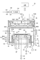
- FIG. 2 is a diagram illustrating an example of a plasma processing apparatus.
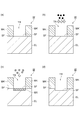
- 3 is a cross-sectional view showing a state of the object to be processed before and after execution of each step shown in FIG. 1, which includes (a) part, (b) part, (c) part, and (d) part. It is.
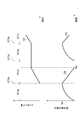
- FIG. 4 is a diagram showing a change in the etching amount with respect to the etching target layer and the thickness of the mixed layer formed in the etching target layer during the execution of the method shown in FIG.
- FIG. 5 is a diagram showing the principle of etching in the method shown in FIG. 1, comprising (a) part, (b) part, and (c) part.
- FIG. 1 is a flow diagram illustrating an embodiment method (method MT).
- a method MT according to an embodiment shown in FIG. 1 is a method for processing an object to be processed (hereinafter also referred to as “wafer”).
- the method MT is an example of a method for etching a wafer.
- a series of steps can be performed using a single plasma processing apparatus (for example, the plasma processing apparatus 10 shown in FIG. 2).
- FIG. 2 is a schematic diagram illustrating the plasma processing apparatus 10 according to an embodiment.
- a plasma processing apparatus 10 shown in FIG. 2 includes an ICP (Inductively Coupled Plasma) type plasma source.
- the plasma processing apparatus 10 includes a processing container 192 formed in a cylindrical shape (for example, a cylindrical shape) made of metal (for example, aluminum).
- the processing container 192 defines a processing space Sp in which plasma processing is performed.
- the shape of the processing container 192 is not limited to a cylindrical shape. For example, a rectangular tube shape (for example, a box shape) may be used.
- the plasma source of the plasma processing apparatus 10 is not limited to the ICP type, and can be, for example, an ECR (Electron Cyclotron Resonance) type, a CCP (Capacitively Coupled Plasma) type, or a type using a microwave. .
- ECR Electro Cyclotron Resonance
- CCP Capacitively Coupled Plasma
- the mounting table PD includes an electrostatic chuck ESC and a lower electrode LE.
- the lower electrode LE includes a first plate 18a and a second plate 18b.
- the processing container 192 defines a processing space Sp.
- the support unit 14 is provided on the bottom of the processing container 192 inside the processing container 192.
- the support part 14 is provided with a substantially cylindrical shape, for example.
- the support part 14 is comprised from an insulating material, for example.
- the insulating material constituting the support portion 14 may contain oxygen like quartz.
- the support portion 14 extends in the vertical direction from the bottom of the processing container 192 in the processing container 192.
- the mounting table PD is provided in the processing container 192.
- the mounting table PD is supported by the support unit 14.
- the mounting table PD holds the wafer W on the upper surface of the mounting table PD.
- the wafer W is an object to be processed.
- the mounting table PD includes a lower electrode LE and an electrostatic chuck ESC.
- the lower electrode LE includes a first plate 18a and a second plate 18b.
- the first plate 18a and the second plate 18b are made of a metal such as aluminum, for example.
- the first plate 18a and the second plate 18b have, for example, a substantially disk shape.
- the second plate 18b is provided on the first plate 18a.
- the second plate 18b is electrically connected to the first plate 18a.
- the electrostatic chuck ESC is provided on the second plate 18b.
- the electrostatic chuck ESC has a structure in which conductive film electrodes are arranged between a pair of insulating layers or between a pair of insulating sheets.
- the DC power supply 22 is electrically connected to the electrode of the electrostatic chuck ESC via the switch 23.
- the electrostatic chuck ESC attracts the wafer W by an electrostatic force generated by a DC voltage from the DC power supply 22. As a result, the electrostatic chuck ESC can hold the wafer W.
- the focus ring FR is disposed on the peripheral edge of the second plate 18b so as to surround the edge of the wafer W and the electrostatic chuck ESC.
- the focus ring FR is provided in order to improve etching uniformity.
- the focus ring FR is made of a material appropriately selected according to the material of the film to be etched, and can be made of, for example, quartz.
- the coolant channel 24 is provided inside the second plate 18b.
- the refrigerant flow path 24 constitutes a temperature adjustment mechanism.
- Refrigerant is supplied to the refrigerant flow path 24 from a chiller unit provided outside the processing container 192 via a pipe 26a.
- the refrigerant supplied to the refrigerant flow path 24 is returned to the chiller unit via the pipe 26b.
- the refrigerant is supplied to the refrigerant flow path 24 so that the refrigerant circulates.
- the gas supply line 28 supplies the heat transfer gas from the heat transfer gas supply mechanism, for example, He gas, between the upper surface of the electrostatic chuck ESC and the back surface of the wafer W.
- the heater HT is a heating element.
- the heater HT is embedded in the second plate 18b.
- the heater power supply HP is connected to the heater HT. By supplying electric power from the heater power supply HP to the heater HT, the temperature of the mounting table PD is adjusted, and the temperature of the wafer W mounted on the mounting table PD is adjusted.
- the heater HT can be incorporated in the electrostatic chuck ESC.
- the plate-like dielectric 194 is disposed opposite the mounting table PD above the mounting table PD.
- the lower electrode LE and the plate-like dielectric 194 are provided substantially parallel to each other.
- a processing space Sp is provided between the plate-like dielectric 194 and the lower electrode LE.
- the processing space Sp is a space region for performing plasma processing on the wafer W.
- a deposition shield 46 is detachably provided along the inner wall of the processing container 192.
- the deposition shield 46 is also provided on the outer periphery of the support portion 14.
- the deposition shield 46 prevents the etching by-product (deposition) from adhering to the processing container 192, and can be configured by coating an aluminum material with ceramics such as Y 2 O 3 .
- the deposition shield can be made of a material containing oxygen such as quartz.
- the exhaust plate 48 is provided on the bottom side of the processing container 192 and between the support portion 14 and the side wall of the processing container 192.
- the exhaust plate 48 can be configured by, for example, coating an aluminum material with ceramics such as Y 2 O 3 .
- the exhaust port 12 e is provided in the processing container 192 below the exhaust plate 48.
- the exhaust device 50 is connected to the exhaust port 12 e via the exhaust pipe 52.
- the exhaust device 50 includes a vacuum pump such as a turbo molecular pump, and can reduce the pressure in the processing container 192 to a desired degree of vacuum.
- the high frequency power source 64 is a power source that generates a second high frequency power for drawing ions into the wafer W, that is, a high frequency bias power, and has a frequency within a range of 400 [kHz] to 40.68 [MHz]. A high frequency bias power of 13 [MHz] is generated.
- the high frequency power supply 64 is connected to the lower electrode LE via the matching unit 68.
- the matching unit 68 is a circuit for matching the output impedance of the high-frequency power source 64 with the input impedance on the load side (lower electrode LE side).
- a plate-like dielectric 194 made of, for example, quartz glass or ceramic is provided on the ceiling of the processing container 192 so as to face the mounting table PD. Specifically, the plate-like dielectric 194 is formed in a disk shape, for example, and is airtightly attached so as to close the opening formed in the ceiling portion of the processing container 192.
- the processing space Sp is a space where plasma is generated by the plasma source.
- the processing space Sp is a space where the wafer W is placed.
- the processing container 192 is provided with a gas supply unit 120 that supplies a first processing gas and a second processing gas described later.
- the gas supply unit 120 supplies the first processing gas and the second processing gas to the processing space Sp described above.
- a gas inlet 121 is formed in the side wall of the processing vessel 192, and a gas supply source 122 is connected to the gas inlet 121 via a gas supply pipe 123.
- a flow rate controller for example, a mass flow controller 124 and an opening / closing valve 126) for controlling the flow rates of the first processing gas and the second processing gas is interposed.
- the first process gas and the second process gas output from the gas supply source 122 are controlled by the mass flow controller 124 to have a preset flow rate, and the gas inlet 121.
- the mass flow controller 124 controls the mass flow controller 124 to have a preset flow rate, and the gas inlet 121.
- the gas supply unit 120 is expressed using a single gas line for the sake of simplicity.
- the gas supply unit 120 includes a plurality of gas types (at least the first processing gas and the first processing gas).
- the second processing gas is provided as a processing gas.
- the gas supply part 120 shown in FIG. 2 is provided with the structure which supplies gas from the side wall part of the processing container 192 as an example, the gas supply part 120 is not restricted to the structure shown in FIG.
- the gas supply unit 120 may be configured to supply gas from the ceiling of the processing container 192.
- a gas introduction port is formed in, for example, the central portion of the plate-like dielectric 194, and gas can be supplied from this gas introduction port.
- An exhaust device 50 that exhausts the atmosphere in the processing container 192 is connected to the bottom of the processing container 192 via an exhaust pipe 52.
- the exhaust device 50 is configured by, for example, a vacuum pump, and can set the pressure in the processing container 192 to a preset pressure.
- a wafer loading / unloading port 134 is provided on the side wall of the processing chamber 192, and a gate valve 136 is provided at the wafer loading / unloading port 134.
- the gate valve 136 is opened, and after the wafer W is mounted on the mounting table PD in the processing container 192 by a transfer mechanism such as a transfer arm (not shown), the gate valve 136 is set. The wafer W is closed and processing of the wafer W is started.
- a planar high-frequency antenna 140 and a shield member 160 that covers the high-frequency antenna 140 are provided on the upper surface (outer surface) of the plate-like dielectric 194 on the ceiling of the processing container 192.
- the high-frequency antenna 140 according to the embodiment includes an inner antenna element 142A disposed at the center of the plate-like dielectric 194 and an outer antenna element 142B disposed so as to surround the outer periphery of the inner antenna element 142A.
- Each of the inner antenna element 142A and the outer antenna element 142B is a conductor such as copper, aluminum, and stainless steel, and has a spiral coil shape.
- Both the inner antenna element 142A and the outer antenna element 142B are sandwiched and integrated with a plurality of sandwiching bodies 144.
- the sandwiching body 144 has, for example, a bar shape.
- the sandwiching body 144 is arranged in a radial pattern so as to project from the vicinity of the center of the inner antenna element 142A to the outside of the outer antenna element 142B.
- the shield member 160 includes an inner shield wall 162A and an outer shield wall 162B.
- the inner shield wall 162A is provided between the inner antenna element 142A and the outer antenna element 142B so as to surround the inner antenna element 142A.
- the outer shield wall 162B is provided so as to surround the outer antenna element 142B, and has a cylindrical shape. Therefore, the upper side surface of the plate-like dielectric 194 is divided into a central portion (central zone) inside the inner shield wall 162A and a peripheral portion (peripheral zone) between the inner shield wall 162A and the outer shield wall 162B. .
- a disc-shaped inner shield plate 164A is provided on the inner antenna element 142A so as to close the opening of the inner shield wall 162A.
- a donut-shaped outer shield plate 164B is provided so as to close an opening between the inner shield wall 162A and the outer shield wall 162B.
- the shape of the shield member 160 is not limited to a cylindrical shape.
- the shape of the shield member 160 can be, for example, another shape such as a rectangular tube shape, or can be adapted to the shape of the processing container 192.
- the processing container 192 has, for example, a substantially cylindrical shape
- the shield member 160 also has a substantially cylindrical shape in accordance with the cylindrical shape.
- the shield member 160 also has a substantially rectangular tube shape.
- the high frequency power supply 150A and the high frequency power supply 150B are separately connected to the inner antenna element 142A and the outer antenna element 142B, respectively. Thereby, high frequency of the same frequency or different frequency can be applied to each of the inner antenna element 142A and the outer antenna element 142B.
- a high frequency of, for example, 27 [MHz] is supplied from the high frequency power supply 150A to the inner antenna element 142A with a preset power [W]
- the processing container is caused by the induced magnetic field formed in the processing container 192.
- the processing gas introduced into 192 is excited, and a donut-shaped plasma can be generated at the center on the wafer W.
- the processing container when a high frequency of, for example, 27 [MHz] or the like is supplied from the high frequency power supply 150B to the outer antenna element 142B with a preset power [W], the processing container is caused by an induction magnetic field formed in the processing container 192. The processing gas introduced into 192 is excited, and another donut-shaped plasma can be generated at the peripheral edge on the wafer W.
- the high frequency output from each of the high frequency power supply 150A and the high frequency power supply 150B is not limited to the above-described frequency, and various high frequencies can be supplied from the high frequency power supply 150A and the high frequency power supply 150B.
- the electrical lengths of the inner antenna element 142A and the outer antenna element 142B need to be adjusted in accordance with the high frequency output from each of the high frequency power supply 150A and the high frequency power supply 150B.
- the height can be adjusted separately by the actuator 168A and the actuator 168B.
- the control unit Cnt is a computer including a processor, a storage unit, an input device, a display device, and the like, and controls each unit of the plasma processing apparatus 10. Specifically, the control unit Cnt is connected to the mass flow controller 124, the opening / closing valve 126, the exhaust device 50, the high frequency power source 150A, the high frequency power source 150B, the high frequency power source 64, the matching unit 68, the heater power source HP, and the chiller unit. .
- the control unit Cnt operates according to a program based on the input recipe and sends out a control signal.
- a control signal from the control unit Cnt at least the selection and flow rate of the gas supplied from the gas supply source 122, the exhaust of the exhaust device 50, and the power supply from the high frequency power supply 150A, the high frequency power supply 150B, and the high frequency power supply 64 It is possible to control the power supply of the heater power supply HP and the refrigerant flow rate and refrigerant temperature from the chiller unit.
- each process of the method (method MT shown in FIG. 1) for processing the target object disclosed in this specification can be executed by operating each part of the plasma processing apparatus 10 under the control of the control unit Cnt. .
- FIG. 3 is a cross-sectional view showing a state of the object to be processed before and after execution of each step shown in FIG. 1, which includes (a) part, (b) part, (c) part, and (d) part. It is.
- FIG. 4 is a diagram showing a change in the etching amount with respect to the etching target layer and the thickness of the mixed layer formed in the etching target layer during the execution of the method shown in FIG.
- FIG. 5 is a diagram showing the principle of etching in the method shown in FIG.
- step ST1 a wafer W shown in FIG. 3A is prepared, and the wafer W is accommodated in the processing container 192 of the plasma processing apparatus 10 and placed on the electrostatic chuck ESC.
- step ST1 the above-described wafer W shown in part (a) of FIG. 3 is prepared as the wafer W shown in FIG. 2, and then each step of sequence SQ and step ST3 is executed.
- a wafer W shown in part (a) of FIG. 3 is provided on a support base (not shown), a layer EL to be etched provided on the support base, and a layer EL to be etched (surface SF of the layer EL to be etched).
- a mask MK, and a trench TR provided in the mask MK.
- the trench TR extends from the surface of the mask MK to the surface SF of the etched layer EL, and exposes the etched layer EL. That is, a part of the surface SF of the layer to be etched EL is exposed through the trench TR.
- the material of the etched layer EL includes an oxide of silicon, and may include, for example, SiO 2 .
- the material of the mask MK can include, for example, TiN.
- a sequence SQ and a series of steps ST3 subsequent to the step ST1 are steps for etching the etching target layer EL.
- the sequence SQ is executed once (unit cycle) or more.
- the sequence SQ is a series of etching that precisely etches a region not covered by the mask MK in the layer to be etched EL with a high selection ratio regardless of the density of the mask MK by a method similar to the ALE (Atomic Layer Etching) method.
- Step ST2a first step
- step ST2b second step
- step ST2c third step
- step ST2d fourth step
- step ST2a plasma of the first processing gas is generated in the processing container 192 of the plasma processing apparatus 10 in which the wafer W is accommodated, and the mixed layer MX containing ions contained in the plasma of the first processing gas is formed. Then, it is formed in the atomic layer of the surface SF of the etched layer EL through the trench TR.
- a bias voltage is applied to the plasma of the first processing gas via the high-frequency power supply 64, and the first processing gas plasma is included in the atomic layer of the surface SF of the etched layer EL.
- a mixed layer MX containing ions may be formed.
- the first processing gas is supplied into the processing container 192, and the first The plasma of the processing gas is generated.
- the first processing gas includes nitrogen, and specifically may include N 2 gas.
- Black circles (black circles) shown in part (b) of FIG. 3 indicate ions (nitrogen atom ions) included in the plasma of the first gas.
- a first processing gas containing N 2 gas is supplied into the processing container 192 from a gas source selected from among a plurality of gas sources of the gas supply source 122.
- the high-frequency power is supplied from the high-frequency power supply 150A and the high-frequency power supply 150B, the high-frequency bias voltage is supplied from the high-frequency power supply 64, and the exhaust device 50 is operated to preset the atmospheric pressure of the processing space Sp in the processing container 192. Set to value.
- the plasma of the first processing gas is generated in the processing container 192, and ions (nitrogen atom ions) contained in the plasma of the first processing gas are attracted in the vertical direction by the high-frequency bias power.
- the surface SF of the etching target layer EL that is in contact with the surface SF of the etching target EL through the trench TR and is exposed through the trench TR is anisotropically modified.
- the anisotropically modified portion of the surface SF of the layer to be etched EL in the process ST2a becomes the mixed layer MX.
- the first gas is N 2 gas and the layer to be etched EL contains silicon oxide (for example, SiO 2 ), the composition of the mixed layer MX can be SiN / SiO 2 (SiON).
- FIG. 5 is a diagram showing the principle of etching in the method (sequence SQ) shown in FIG. 1, which includes the parts (a), (b), and (c).
- white circles (white circles) indicate atoms (for example, atoms constituting SiO 2 ) constituting the layer to be etched EL, and black circles (black circles) indicate the plasma of the first gas.
- the “x” surrounded by a circle indicates a radical contained in the plasma of the second gas described later.
- step ST2a ions of nitrogen atoms (black circles (black circles)) contained in the plasma of the first gas are transferred into the trench TR.
- the mixed layer MX including the atoms constituting the layer to be etched EL and the nitrogen atoms of the first gas is formed on the atomic layer of the surface SF of the layer to be etched EL exposed by the trench TR by the step ST2a. (See also (c) part of FIG. 3 together with (a) part of FIG. 5).
- step ST2a nitrogen atoms are supplied to the atomic layer (atomic layer of silicon oxide) on the surface SF of the etched layer EL, and silicon nitride A mixed layer MX (SiN / SiO 2 ) containing can be formed in the atomic layer of the surface SF.
- step ST2b the processing space Sp in the processing container 192 is purged. Specifically, the first processing gas supplied in step ST2a is exhausted.
- an inert gas such as a rare gas (eg, Ar gas) may be supplied to the processing container 192 as a purge gas. That is, the purge in the step ST2b may be either a gas purge for flowing an inert gas into the processing container 192 or a purge by evacuation.
- step ST2c subsequent to step ST2b, plasma of the second processing gas is generated in the processing container 192, and the mixed layer MX is removed by chemical etching using radicals contained in the plasma.
- step ST2c as shown in part (c) of FIG. 3, the wafer W after the formation of the mixed layer MX in step ST2a is placed on the electrostatic chuck ESC in the processing container 192.
- a second processing gas is supplied, and plasma of the second processing gas is generated.
- the plasma of the second processing gas generated in the step ST2c includes radicals that remove the mixed layer MX containing silicon nitride. “X” surrounded by a circle shown in part (c) of FIG. 3 indicates radicals contained in the plasma of the second gas.
- the second processing gas includes fluorine, and may be a mixed gas including, for example, NF 3 gas and O 2 gas.
- the second processing gas is also a mixed gas containing NF 3 gas, O 2 gas, H 2 gas, and Ar gas, and a mixed gas containing CH 3 F gas, O 2 gas, and Ar gas.
- the second processing gas is supplied into the processing container 192 from a gas source selected from the gas sources of the gas supply source 122, and high-frequency power is supplied from the high-frequency power source 150A and the high-frequency power source 150B.
- the atmospheric pressure of the processing space Sp in the processing container 192 is set to a preset value. In this manner, plasma of the second processing gas is generated in the processing container 192.
- the radicals in the plasma of the second processing gas generated in step ST2c come into contact with the mixed layer MX on the surface SF of the layer to be etched EL through the trench TR.
- the radical ST of the second process gas is supplied to the mixed layer MX formed on the surface SF of the etched layer EL by the process ST2c, and the mixed layer MX is chemically etched. Can be removed from the etched layer EL.
- the mixed layer MX formed on the surface SF of the etched layer EL is caused by radicals contained in the plasma of the second processing gas. It can be removed from the surface SF of the etched layer EL.
- step ST2d subsequent to step ST2c, the processing space Sp in the processing container 192 is purged. Specifically, the second processing gas supplied in step ST2c is exhausted.
- an inert gas such as a rare gas (eg, Ar gas) may be supplied to the processing container 192 as a purge gas.
- the purge in step ST2d may be either a gas purge for flowing an inert gas into the processing container 192 or a purge by evacuation.
- step ST3 it is determined whether or not to end the execution of the sequence SQ. Specifically, in step ST3, it is determined whether or not the number of executions of the sequence SQ has reached a preset number.
- the determination of the number of execution times of the sequence SQ is to determine the etching amount for the etching target layer EL (the depth of the groove formed in the etching target layer EL by etching).
- the sequence SQ can be repeatedly executed so that the etching target layer EL is etched until the etching amount with respect to the etching target layer EL reaches a preset value. As the number of executions of the sequence SQ increases, the etching amount for the etching target layer EL also increases (substantially linearly increases).
- the product of the thickness of the layer EL to be etched (the thickness of the mixed layer MX formed in one step ST2a) and the number of executions of the sequence SQ is determined in advance by executing the sequence SQ once (unit cycle).
- the number of executions of the sequence SQ can be determined so as to be a set value.
- a graph G1 in FIG. 4 shows a change in an etching amount (arbitrary unit) with respect to the etching target layer EL generated during the execution of the sequence SQ
- a graph G2 in FIG. 4 shows an etching target layer EL generated during the execution of the sequence SQ.
- the change of the thickness (arbitrary unit) of the mixed layer MX formed in FIG. The horizontal axis of FIG.
- the execution of the step ST2a is performed until the thickness of the mixed layer MX reaches a preset value TH as shown in the graph G2.
- the value TH of the thickness of the mixed layer MX formed in the step ST2a is the value of the bias power applied by the high frequency power supply 64 and the unit time of the ions contained in the plasma of the first gas with respect to the layer to be etched EL. Can be determined by the amount of dose and the execution time of the process ST2a.
- the execution of the step ST2c removes all the mixed layer MX formed in the step ST2a as shown in the graph G1 and the graph G2. It is done until it is done.
- the mixed layer MX is completely removed by chemical etching before the timing TM is reached during the execution of the process ST2b.
- the timing TM can be determined by the etching rate of chemical etching performed in step ST2c.
- the timing TM is generated during the execution of the process ST2b. Between the timing TM and the end of the process ST2b, the etched layer EL of the silicon oxide after the removal of the mixed layer MX is not etched by the plasma of the second processing gas (self-limited).
- the etching rate of etching with respect to silicon oxide (for example, SiO 2 ) constituting the etched layer EL is the nitridation of silicon contained in the mixed layer MX. Compared to the etching rate of etching with respect to an object (for example, SiN), it is extremely small.
- step ST3 When it is determined in step ST3 that the number of executions of the sequence SQ has not reached the preset number (step ST3: NO), the execution of the sequence SQ is repeated again. On the other hand, when it is determined in step ST3 that the number of executions of the sequence SQ has reached the preset number (step ST3: YES), the execution of the sequence SQ is ended.
- the sequence SQ and the series of steps ST3 are performed by repeatedly executing the sequence SQ using the mask MK to remove the layer to be etched EL for each atomic layer, thereby increasing the pattern density of the mask MK and the width of the trench TR. Regardless of (value), this is a step of precisely etching the layer to be etched EL.
- the sequence SQ is repeated a predetermined number of times, so that the layer to be etched EL is provided with the trench TR provided by the mask MK regardless of the pattern density of the mask MK and the width (value) of the trench TR.
- the layer to be etched EL can be removed for each atomic layer by a method similar to the ALE method.
- the first process for the etched layer EL is performed while maintaining a relatively large etching amount of silicon nitride relative to the silicon oxide in the etched layer EL. It has been found by the inventors that the amount of sputtering by gas plasma can be sufficiently reduced.
- the second processing gas may be a mixed gas of NF 3 gas, O 2 gas, H 2 gas, and Ar gas.
- the following process conditions can be used in step ST2c.
- the value [W] of the high frequency power of the high frequency power source 64 0 [W] (13 [MHz])
- Second processing gas mixed gas containing NF 3 gas and O 2 gas
- the ICP type plasma source has been described as an example.
- the plasma source of the plasma processing apparatus 10 is not limited to the ICP type, and a CCP type can also be used.
- examples of main process conditions of the process ST2a and the process ST2c when the plasma source of the plasma processing apparatus 10 is the CCP type will be described.
- ashing may be further performed under the following process conditions after step ST2c.
- Second processing gas O 2 gas Flow rate of second processing gas [sccm]: 750 [sccm] Processing time [s]: 60 [s]
- step ST2a of the sequence SQ that is repeatedly executed, first, nitrogen is contained with respect to the surface SF of the etched layer EL including the silicon oxide exposed through the trench TR of the mask MK.
- the mixed layer MX containing nitrogen ions is formed by the plasma of the first processing gas.
- the mixed layer MX contains silicon nitride.
- step ST2c of sequence SQ the silicon nitride mixed layer MX formed in step ST2a is removed using radicals contained in the plasma of the second processing gas containing fluorine.
- step ST2a in which the first gas containing nitrogen is used, the mixed layer MX containing silicon nitride is formed along the shape of the opening of the trench TR of the mask MK in detail, and the second layer containing fluorine.
- step ST2c in which a gas is used, the mixed layer MX is removed from the etched layer EL. Therefore, it is possible to etch the etched layer EL in a state where the shape of the opening of the trench TR of the mask MK is maintained in detail while avoiding the formation of deposits on the opening and side surfaces of the trench TR of the mask MK.
- the etched layer EL can be etched uniformly regardless of the width of the trench TR of the mask MK and the density of the pattern of the trench TR of the mask MK. Further, the sequence SQ including the steps ST2a and ST2c is repeatedly executed, so that the shape of the opening of the trench TR of the mask MK is maintained in detail, and the width of the trench TR and the mask MK of the mask MK are maintained.
- the layer to be etched EL can be etched uniformly to a desired depth regardless of the density of the trench TR pattern.
- SYMBOLS 10 Plasma processing apparatus, 120 ... Gas supply part, 121 ... Gas introduction port, 122 ... Gas supply source, 123 ... Gas supply piping, 124 ... Mass flow controller, 126 ... Open / close valve, 12e ... Exhaust port, 134 ... Wafer carry-in / out port DESCRIPTION OF SYMBOLS 136 ... Gate valve, 14 ... Support part, 140 ... High frequency antenna, 142A ... Inner antenna element, 142B ... Outer antenna element, 144 ... Holding body, 150A ... High frequency power source, 150B ... High frequency power source, 160 ... Shield member, 162A ... Inner shield wall, 162B ...
- outer shield wall 164A ... inner shield plate, 164B ... outer shield plate, 168A ... actuator, 168B ... actuator, 18a ... first plate, 18b ... second plate, 192 ... processing vessel, 194 ... plate Dielectric, 22 ... DC power supply, 23 ... switch, 4 ... refrigerant flow path, 26a ... piping, 26b ... piping, 28 ... gas supply line, 46 ... depot shield, 48 ... exhaust plate, 50 ... exhaust device, 52 ... exhaust pipe, 64 ... high frequency power supply, 68 ...
Landscapes
- Engineering & Computer Science (AREA)
- Physics & Mathematics (AREA)
- Plasma & Fusion (AREA)
- Chemical & Material Sciences (AREA)
- Condensed Matter Physics & Semiconductors (AREA)
- General Physics & Mathematics (AREA)
- Manufacturing & Machinery (AREA)
- Computer Hardware Design (AREA)
- Microelectronics & Electronic Packaging (AREA)
- Power Engineering (AREA)
- Analytical Chemistry (AREA)
- Chemical Kinetics & Catalysis (AREA)
- General Chemical & Material Sciences (AREA)
- Inorganic Chemistry (AREA)
- Electromagnetism (AREA)
- Spectroscopy & Molecular Physics (AREA)
- Drying Of Semiconductors (AREA)
- High Energy & Nuclear Physics (AREA)
- Health & Medical Sciences (AREA)
- Toxicology (AREA)
- Plasma Technology (AREA)
Priority Applications (5)
| Application Number | Priority Date | Filing Date | Title |
|---|---|---|---|
| CN201780068805.1A CN109923648B (zh) | 2016-11-07 | 2017-11-02 | 处理被处理体的方法 |
| KR1020237028539A KR20230127373A (ko) | 2016-11-07 | 2017-11-02 | 피처리체를 처리하는 방법 |
| KR1020197013091A KR102571380B1 (ko) | 2016-11-07 | 2017-11-02 | 피처리체를 처리하는 방법 |
| US16/347,697 US11081360B2 (en) | 2016-11-07 | 2017-11-02 | Method for processing workpiece |
| US17/362,285 US20210327719A1 (en) | 2016-11-07 | 2021-06-29 | Method for processing workpiece |
Applications Claiming Priority (2)
| Application Number | Priority Date | Filing Date | Title |
|---|---|---|---|
| JP2016217163A JP6763750B2 (ja) | 2016-11-07 | 2016-11-07 | 被処理体を処理する方法 |
| JP2016-217163 | 2016-11-07 |
Related Child Applications (2)
| Application Number | Title | Priority Date | Filing Date |
|---|---|---|---|
| US16/347,697 A-371-Of-International US11081360B2 (en) | 2016-11-07 | 2017-11-02 | Method for processing workpiece |
| US17/362,285 Continuation US20210327719A1 (en) | 2016-11-07 | 2021-06-29 | Method for processing workpiece |
Publications (1)
| Publication Number | Publication Date |
|---|---|
| WO2018084255A1 true WO2018084255A1 (ja) | 2018-05-11 |
Family
ID=62076951
Family Applications (1)
| Application Number | Title | Priority Date | Filing Date |
|---|---|---|---|
| PCT/JP2017/039772 WO2018084255A1 (ja) | 2016-11-07 | 2017-11-02 | 被処理体を処理する方法 |
Country Status (6)
| Country | Link |
|---|---|
| US (2) | US11081360B2 (zh) |
| JP (1) | JP6763750B2 (zh) |
| KR (2) | KR20230127373A (zh) |
| CN (1) | CN109923648B (zh) |
| TW (1) | TWI759348B (zh) |
| WO (1) | WO2018084255A1 (zh) |
Families Citing this family (2)
| Publication number | Priority date | Publication date | Assignee | Title |
|---|---|---|---|---|
| JP7066565B2 (ja) * | 2018-07-27 | 2022-05-13 | 東京エレクトロン株式会社 | プラズマ処理方法およびプラズマ処理装置 |
| US10950428B1 (en) * | 2019-08-30 | 2021-03-16 | Mattson Technology, Inc. | Method for processing a workpiece |
Citations (3)
| Publication number | Priority date | Publication date | Assignee | Title |
|---|---|---|---|---|
| JP2001210627A (ja) * | 1999-11-16 | 2001-08-03 | Matsushita Electric Ind Co Ltd | エッチング方法、半導体装置及びその製造方法 |
| JP2016015382A (ja) * | 2014-07-01 | 2016-01-28 | 東京エレクトロン株式会社 | エッチング方法、エッチング装置及び記憶媒体 |
| JP2016127285A (ja) * | 2015-01-06 | 2016-07-11 | ラム リサーチ コーポレーションLam Research Corporation | 活性化を使用しない、シリコン酸化物のための異方性原子層エッチング |
Family Cites Families (13)
| Publication number | Priority date | Publication date | Assignee | Title |
|---|---|---|---|---|
| KR100276736B1 (ko) * | 1993-10-20 | 2001-03-02 | 히가시 데쓰로 | 플라즈마 처리장치 |
| US5786276A (en) * | 1997-03-31 | 1998-07-28 | Applied Materials, Inc. | Selective plasma etching of silicon nitride in presence of silicon or silicon oxides using mixture of CH3F or CH2F2 and CF4 and O2 |
| US5942446A (en) * | 1997-09-12 | 1999-08-24 | Taiwan Semiconductor Manufacturing Company, Ltd. | Fluorocarbon polymer layer deposition predominant pre-etch plasma etch method for forming patterned silicon containing dielectric layer |
| KR100480610B1 (ko) | 2002-08-09 | 2005-03-31 | 삼성전자주식회사 | 실리콘 산화막을 이용한 미세 패턴 형성방법 |
| JP2013258244A (ja) * | 2012-06-12 | 2013-12-26 | Tokyo Electron Ltd | エッチング方法及びプラズマ処理装置 |
| JP5982223B2 (ja) * | 2012-08-27 | 2016-08-31 | 東京エレクトロン株式会社 | プラズマ処理方法、及びプラズマ処理装置 |
| US8956980B1 (en) * | 2013-09-16 | 2015-02-17 | Applied Materials, Inc. | Selective etch of silicon nitride |
| JP2015084396A (ja) * | 2013-09-19 | 2015-04-30 | 東京エレクトロン株式会社 | エッチング方法 |
| JP6277004B2 (ja) * | 2014-01-31 | 2018-02-07 | 株式会社日立ハイテクノロジーズ | ドライエッチング方法 |
| US9548303B2 (en) * | 2014-03-13 | 2017-01-17 | Taiwan Semiconductor Manufacturing Company, Ltd. | FinFET devices with unique fin shape and the fabrication thereof |
| US9142459B1 (en) * | 2014-06-30 | 2015-09-22 | Applied Materials, Inc. | Wafer dicing using hybrid laser scribing and plasma etch approach with mask application by vacuum lamination |
| JP6366454B2 (ja) * | 2014-10-07 | 2018-08-01 | 東京エレクトロン株式会社 | 被処理体を処理する方法 |
| JP6339963B2 (ja) * | 2015-04-06 | 2018-06-06 | 東京エレクトロン株式会社 | エッチング方法 |
-
2016
- 2016-11-07 JP JP2016217163A patent/JP6763750B2/ja active Active
-
2017
- 2017-10-31 TW TW106137484A patent/TWI759348B/zh active
- 2017-11-02 KR KR1020237028539A patent/KR20230127373A/ko not_active Application Discontinuation
- 2017-11-02 US US16/347,697 patent/US11081360B2/en active Active
- 2017-11-02 CN CN201780068805.1A patent/CN109923648B/zh active Active
- 2017-11-02 WO PCT/JP2017/039772 patent/WO2018084255A1/ja active Application Filing
- 2017-11-02 KR KR1020197013091A patent/KR102571380B1/ko active IP Right Grant
-
2021
- 2021-06-29 US US17/362,285 patent/US20210327719A1/en active Pending
Patent Citations (3)
| Publication number | Priority date | Publication date | Assignee | Title |
|---|---|---|---|---|
| JP2001210627A (ja) * | 1999-11-16 | 2001-08-03 | Matsushita Electric Ind Co Ltd | エッチング方法、半導体装置及びその製造方法 |
| JP2016015382A (ja) * | 2014-07-01 | 2016-01-28 | 東京エレクトロン株式会社 | エッチング方法、エッチング装置及び記憶媒体 |
| JP2016127285A (ja) * | 2015-01-06 | 2016-07-11 | ラム リサーチ コーポレーションLam Research Corporation | 活性化を使用しない、シリコン酸化物のための異方性原子層エッチング |
Also Published As
| Publication number | Publication date |
|---|---|
| KR20230127373A (ko) | 2023-08-31 |
| CN109923648A (zh) | 2019-06-21 |
| US11081360B2 (en) | 2021-08-03 |
| TW201829835A (zh) | 2018-08-16 |
| US20190259627A1 (en) | 2019-08-22 |
| KR20190075952A (ko) | 2019-07-01 |
| US20210327719A1 (en) | 2021-10-21 |
| TWI759348B (zh) | 2022-04-01 |
| JP2018078138A (ja) | 2018-05-17 |
| JP6763750B2 (ja) | 2020-09-30 |
| CN109923648B (zh) | 2023-06-23 |
| KR102571380B1 (ko) | 2023-08-25 |
Similar Documents
| Publication | Publication Date | Title |
|---|---|---|
| US11380551B2 (en) | Method of processing target object | |
| US11145518B2 (en) | Method and apparatus for etching target object | |
| US20200185238A1 (en) | Apparatus for selectively etching first region made of silicon nitride against second region made of silicon oxide | |
| US9911607B2 (en) | Method of processing target object | |
| US11462412B2 (en) | Etching method | |
| KR20230129345A (ko) | 플라즈마 처리 장치 및 에칭 방법 | |
| US20210327719A1 (en) | Method for processing workpiece | |
| JP2019186501A (ja) | エッチングする方法及びプラズマ処理装置 | |
| CN109075068B (zh) | 蚀刻方法 |
Legal Events
| Date | Code | Title | Description |
|---|---|---|---|
| 121 | Ep: the epo has been informed by wipo that ep was designated in this application |
Ref document number: 17867438 Country of ref document: EP Kind code of ref document: A1 |
|
| ENP | Entry into the national phase |
Ref document number: 20197013091 Country of ref document: KR Kind code of ref document: A |
|
| NENP | Non-entry into the national phase |
Ref country code: DE |
|
| 122 | Ep: pct application non-entry in european phase |
Ref document number: 17867438 Country of ref document: EP Kind code of ref document: A1 |