WO2018084255A1 - 被処理体を処理する方法 - Google Patents
被処理体を処理する方法 Download PDFInfo
- Publication number
- WO2018084255A1 WO2018084255A1 PCT/JP2017/039772 JP2017039772W WO2018084255A1 WO 2018084255 A1 WO2018084255 A1 WO 2018084255A1 JP 2017039772 W JP2017039772 W JP 2017039772W WO 2018084255 A1 WO2018084255 A1 WO 2018084255A1
- Authority
- WO
- WIPO (PCT)
- Prior art keywords
- gas
- layer
- processing
- etched
- plasma
- Prior art date
Links
- 238000000034 method Methods 0.000 title claims abstract description 74
- 239000007789 gas Substances 0.000 claims abstract description 215
- IJGRMHOSHXDMSA-UHFFFAOYSA-N Atomic nitrogen Chemical compound N#N IJGRMHOSHXDMSA-UHFFFAOYSA-N 0.000 claims abstract description 18
- 229910052757 nitrogen Inorganic materials 0.000 claims abstract description 14
- PXGOKWXKJXAPGV-UHFFFAOYSA-N Fluorine Chemical compound FF PXGOKWXKJXAPGV-UHFFFAOYSA-N 0.000 claims abstract description 9
- 229910052731 fluorine Inorganic materials 0.000 claims abstract description 9
- 239000011737 fluorine Substances 0.000 claims abstract description 9
- 229910052710 silicon Inorganic materials 0.000 claims abstract description 6
- 239000010703 silicon Substances 0.000 claims abstract description 6
- 238000005530 etching Methods 0.000 claims description 60
- 150000002500 ions Chemical class 0.000 claims description 13
- 229910052581 Si3N4 Inorganic materials 0.000 claims description 12
- 238000010926 purge Methods 0.000 claims description 12
- HQVNEWCFYHHQES-UHFFFAOYSA-N silicon nitride Chemical compound N12[Si]34N5[Si]62N3[Si]51N64 HQVNEWCFYHHQES-UHFFFAOYSA-N 0.000 claims description 12
- 239000000203 mixture Substances 0.000 abstract description 4
- 150000004767 nitrides Chemical class 0.000 abstract 1
- VYPSYNLAJGMNEJ-UHFFFAOYSA-N Silicium dioxide Chemical compound O=[Si]=O VYPSYNLAJGMNEJ-UHFFFAOYSA-N 0.000 description 16
- 229910052814 silicon oxide Inorganic materials 0.000 description 13
- 239000003507 refrigerant Substances 0.000 description 12
- 101001090150 Equus caballus Sperm histone P2a Proteins 0.000 description 9
- 238000010586 diagram Methods 0.000 description 9
- 229910004298 SiO 2 Inorganic materials 0.000 description 8
- 239000000463 material Substances 0.000 description 7
- 238000000151 deposition Methods 0.000 description 6
- -1 nitrogen ions Chemical class 0.000 description 6
- 101001016600 Equus caballus Sperm histone P2b Proteins 0.000 description 5
- 229910052782 aluminium Inorganic materials 0.000 description 5
- XAGFODPZIPBFFR-UHFFFAOYSA-N aluminium Chemical compound [Al] XAGFODPZIPBFFR-UHFFFAOYSA-N 0.000 description 5
- 230000008021 deposition Effects 0.000 description 5
- 238000009616 inductively coupled plasma Methods 0.000 description 5
- 239000011261 inert gas Substances 0.000 description 4
- 230000002093 peripheral effect Effects 0.000 description 4
- XUIMIQQOPSSXEZ-UHFFFAOYSA-N Silicon Chemical compound [Si] XUIMIQQOPSSXEZ-UHFFFAOYSA-N 0.000 description 3
- 125000004429 atom Chemical group 0.000 description 3
- 230000015572 biosynthetic process Effects 0.000 description 3
- 239000000919 ceramic Substances 0.000 description 3
- 238000003486 chemical etching Methods 0.000 description 3
- 125000004433 nitrogen atom Chemical group N* 0.000 description 3
- 239000010453 quartz Substances 0.000 description 3
- 238000004380 ashing Methods 0.000 description 2
- QVGXLLKOCUKJST-UHFFFAOYSA-N atomic oxygen Chemical compound [O] QVGXLLKOCUKJST-UHFFFAOYSA-N 0.000 description 2
- 239000011248 coating agent Substances 0.000 description 2
- 238000000576 coating method Methods 0.000 description 2
- 239000011810 insulating material Substances 0.000 description 2
- 230000010354 integration Effects 0.000 description 2
- 229910052751 metal Inorganic materials 0.000 description 2
- 239000002184 metal Substances 0.000 description 2
- 239000001301 oxygen Substances 0.000 description 2
- 229910052760 oxygen Inorganic materials 0.000 description 2
- 238000000206 photolithography Methods 0.000 description 2
- 238000001020 plasma etching Methods 0.000 description 2
- RYGMFSIKBFXOCR-UHFFFAOYSA-N Copper Chemical compound [Cu] RYGMFSIKBFXOCR-UHFFFAOYSA-N 0.000 description 1
- 108091081062 Repeated sequence (DNA) Proteins 0.000 description 1
- ATJFFYVFTNAWJD-UHFFFAOYSA-N Tin Chemical compound [Sn] ATJFFYVFTNAWJD-UHFFFAOYSA-N 0.000 description 1
- 239000006227 byproduct Substances 0.000 description 1
- 239000004020 conductor Substances 0.000 description 1
- 239000002826 coolant Substances 0.000 description 1
- 229910052802 copper Inorganic materials 0.000 description 1
- 239000010949 copper Substances 0.000 description 1
- 238000010438 heat treatment Methods 0.000 description 1
- 230000006698 induction Effects 0.000 description 1
- 238000012986 modification Methods 0.000 description 1
- 230000004048 modification Effects 0.000 description 1
- 239000000047 product Substances 0.000 description 1
- 230000007261 regionalization Effects 0.000 description 1
- 238000004544 sputter deposition Methods 0.000 description 1
- 229910001220 stainless steel Inorganic materials 0.000 description 1
- 239000010935 stainless steel Substances 0.000 description 1
Images

Classifications
-
- H—ELECTRICITY
- H01—ELECTRIC ELEMENTS
- H01L—SEMICONDUCTOR DEVICES NOT COVERED BY CLASS H10
- H01L21/00—Processes or apparatus adapted for the manufacture or treatment of semiconductor or solid state devices or of parts thereof
- H01L21/67—Apparatus specially adapted for handling semiconductor or electric solid state devices during manufacture or treatment thereof; Apparatus specially adapted for handling wafers during manufacture or treatment of semiconductor or electric solid state devices or components ; Apparatus not specifically provided for elsewhere
- H01L21/67005—Apparatus not specifically provided for elsewhere
- H01L21/67011—Apparatus for manufacture or treatment
- H01L21/67017—Apparatus for fluid treatment
- H01L21/67063—Apparatus for fluid treatment for etching
- H01L21/67069—Apparatus for fluid treatment for etching for drying etching
-
- H—ELECTRICITY
- H01—ELECTRIC ELEMENTS
- H01J—ELECTRIC DISCHARGE TUBES OR DISCHARGE LAMPS
- H01J37/00—Discharge tubes with provision for introducing objects or material to be exposed to the discharge, e.g. for the purpose of examination or processing thereof
- H01J37/32—Gas-filled discharge tubes
- H01J37/32009—Arrangements for generation of plasma specially adapted for examination or treatment of objects, e.g. plasma sources
- H01J37/32082—Radio frequency generated discharge
- H01J37/32091—Radio frequency generated discharge the radio frequency energy being capacitively coupled to the plasma
-
- H—ELECTRICITY
- H01—ELECTRIC ELEMENTS
- H01J—ELECTRIC DISCHARGE TUBES OR DISCHARGE LAMPS
- H01J37/00—Discharge tubes with provision for introducing objects or material to be exposed to the discharge, e.g. for the purpose of examination or processing thereof
- H01J37/32—Gas-filled discharge tubes
- H01J37/32009—Arrangements for generation of plasma specially adapted for examination or treatment of objects, e.g. plasma sources
- H01J37/32082—Radio frequency generated discharge
- H01J37/321—Radio frequency generated discharge the radio frequency energy being inductively coupled to the plasma
- H01J37/3211—Antennas, e.g. particular shapes of coils
-
- H—ELECTRICITY
- H01—ELECTRIC ELEMENTS
- H01J—ELECTRIC DISCHARGE TUBES OR DISCHARGE LAMPS
- H01J37/00—Discharge tubes with provision for introducing objects or material to be exposed to the discharge, e.g. for the purpose of examination or processing thereof
- H01J37/32—Gas-filled discharge tubes
- H01J37/32009—Arrangements for generation of plasma specially adapted for examination or treatment of objects, e.g. plasma sources
- H01J37/32192—Microwave generated discharge
-
- H—ELECTRICITY
- H01—ELECTRIC ELEMENTS
- H01J—ELECTRIC DISCHARGE TUBES OR DISCHARGE LAMPS
- H01J37/00—Discharge tubes with provision for introducing objects or material to be exposed to the discharge, e.g. for the purpose of examination or processing thereof
- H01J37/32—Gas-filled discharge tubes
- H01J37/32431—Constructional details of the reactor
- H01J37/3244—Gas supply means
- H01J37/32449—Gas control, e.g. control of the gas flow
-
- H—ELECTRICITY
- H01—ELECTRIC ELEMENTS
- H01J—ELECTRIC DISCHARGE TUBES OR DISCHARGE LAMPS
- H01J37/00—Discharge tubes with provision for introducing objects or material to be exposed to the discharge, e.g. for the purpose of examination or processing thereof
- H01J37/32—Gas-filled discharge tubes
- H01J37/32431—Constructional details of the reactor
- H01J37/32715—Workpiece holder
- H01J37/32724—Temperature
-
- H—ELECTRICITY
- H01—ELECTRIC ELEMENTS
- H01L—SEMICONDUCTOR DEVICES NOT COVERED BY CLASS H10
- H01L21/00—Processes or apparatus adapted for the manufacture or treatment of semiconductor or solid state devices or of parts thereof
- H01L21/02—Manufacture or treatment of semiconductor devices or of parts thereof
- H01L21/02104—Forming layers
- H01L21/02107—Forming insulating materials on a substrate
- H01L21/02109—Forming insulating materials on a substrate characterised by the type of layer, e.g. type of material, porous/non-porous, pre-cursors, mixtures or laminates
- H01L21/02112—Forming insulating materials on a substrate characterised by the type of layer, e.g. type of material, porous/non-porous, pre-cursors, mixtures or laminates characterised by the material of the layer
- H01L21/02123—Forming insulating materials on a substrate characterised by the type of layer, e.g. type of material, porous/non-porous, pre-cursors, mixtures or laminates characterised by the material of the layer the material containing silicon
- H01L21/02164—Forming insulating materials on a substrate characterised by the type of layer, e.g. type of material, porous/non-porous, pre-cursors, mixtures or laminates characterised by the material of the layer the material containing silicon the material being a silicon oxide, e.g. SiO2
-
- H—ELECTRICITY
- H01—ELECTRIC ELEMENTS
- H01L—SEMICONDUCTOR DEVICES NOT COVERED BY CLASS H10
- H01L21/00—Processes or apparatus adapted for the manufacture or treatment of semiconductor or solid state devices or of parts thereof
- H01L21/02—Manufacture or treatment of semiconductor devices or of parts thereof
- H01L21/02104—Forming layers
- H01L21/02107—Forming insulating materials on a substrate
- H01L21/02296—Forming insulating materials on a substrate characterised by the treatment performed before or after the formation of the layer
- H01L21/02318—Forming insulating materials on a substrate characterised by the treatment performed before or after the formation of the layer post-treatment
- H01L21/02321—Forming insulating materials on a substrate characterised by the treatment performed before or after the formation of the layer post-treatment introduction of substances into an already existing insulating layer
- H01L21/02329—Forming insulating materials on a substrate characterised by the treatment performed before or after the formation of the layer post-treatment introduction of substances into an already existing insulating layer introduction of nitrogen
- H01L21/02332—Forming insulating materials on a substrate characterised by the treatment performed before or after the formation of the layer post-treatment introduction of substances into an already existing insulating layer introduction of nitrogen into an oxide layer, e.g. changing SiO to SiON
-
- H—ELECTRICITY
- H01—ELECTRIC ELEMENTS
- H01L—SEMICONDUCTOR DEVICES NOT COVERED BY CLASS H10
- H01L21/00—Processes or apparatus adapted for the manufacture or treatment of semiconductor or solid state devices or of parts thereof
- H01L21/02—Manufacture or treatment of semiconductor devices or of parts thereof
- H01L21/04—Manufacture or treatment of semiconductor devices or of parts thereof the devices having potential barriers, e.g. a PN junction, depletion layer or carrier concentration layer
- H01L21/18—Manufacture or treatment of semiconductor devices or of parts thereof the devices having potential barriers, e.g. a PN junction, depletion layer or carrier concentration layer the devices having semiconductor bodies comprising elements of Group IV of the Periodic Table or AIIIBV compounds with or without impurities, e.g. doping materials
- H01L21/30—Treatment of semiconductor bodies using processes or apparatus not provided for in groups H01L21/20 - H01L21/26
- H01L21/302—Treatment of semiconductor bodies using processes or apparatus not provided for in groups H01L21/20 - H01L21/26 to change their surface-physical characteristics or shape, e.g. etching, polishing, cutting
- H01L21/306—Chemical or electrical treatment, e.g. electrolytic etching
- H01L21/3065—Plasma etching; Reactive-ion etching
-
- H—ELECTRICITY
- H01—ELECTRIC ELEMENTS
- H01L—SEMICONDUCTOR DEVICES NOT COVERED BY CLASS H10
- H01L21/00—Processes or apparatus adapted for the manufacture or treatment of semiconductor or solid state devices or of parts thereof
- H01L21/02—Manufacture or treatment of semiconductor devices or of parts thereof
- H01L21/04—Manufacture or treatment of semiconductor devices or of parts thereof the devices having potential barriers, e.g. a PN junction, depletion layer or carrier concentration layer
- H01L21/18—Manufacture or treatment of semiconductor devices or of parts thereof the devices having potential barriers, e.g. a PN junction, depletion layer or carrier concentration layer the devices having semiconductor bodies comprising elements of Group IV of the Periodic Table or AIIIBV compounds with or without impurities, e.g. doping materials
- H01L21/30—Treatment of semiconductor bodies using processes or apparatus not provided for in groups H01L21/20 - H01L21/26
- H01L21/31—Treatment of semiconductor bodies using processes or apparatus not provided for in groups H01L21/20 - H01L21/26 to form insulating layers thereon, e.g. for masking or by using photolithographic techniques; After treatment of these layers; Selection of materials for these layers
- H01L21/3105—After-treatment
- H01L21/311—Etching the insulating layers by chemical or physical means
- H01L21/31105—Etching inorganic layers
- H01L21/31111—Etching inorganic layers by chemical means
- H01L21/31116—Etching inorganic layers by chemical means by dry-etching
-
- H—ELECTRICITY
- H01—ELECTRIC ELEMENTS
- H01L—SEMICONDUCTOR DEVICES NOT COVERED BY CLASS H10
- H01L21/00—Processes or apparatus adapted for the manufacture or treatment of semiconductor or solid state devices or of parts thereof
- H01L21/02—Manufacture or treatment of semiconductor devices or of parts thereof
- H01L21/04—Manufacture or treatment of semiconductor devices or of parts thereof the devices having potential barriers, e.g. a PN junction, depletion layer or carrier concentration layer
- H01L21/18—Manufacture or treatment of semiconductor devices or of parts thereof the devices having potential barriers, e.g. a PN junction, depletion layer or carrier concentration layer the devices having semiconductor bodies comprising elements of Group IV of the Periodic Table or AIIIBV compounds with or without impurities, e.g. doping materials
- H01L21/30—Treatment of semiconductor bodies using processes or apparatus not provided for in groups H01L21/20 - H01L21/26
- H01L21/31—Treatment of semiconductor bodies using processes or apparatus not provided for in groups H01L21/20 - H01L21/26 to form insulating layers thereon, e.g. for masking or by using photolithographic techniques; After treatment of these layers; Selection of materials for these layers
- H01L21/3105—After-treatment
- H01L21/311—Etching the insulating layers by chemical or physical means
- H01L21/31144—Etching the insulating layers by chemical or physical means using masks
-
- H—ELECTRICITY
- H01—ELECTRIC ELEMENTS
- H01L—SEMICONDUCTOR DEVICES NOT COVERED BY CLASS H10
- H01L21/00—Processes or apparatus adapted for the manufacture or treatment of semiconductor or solid state devices or of parts thereof
- H01L21/67—Apparatus specially adapted for handling semiconductor or electric solid state devices during manufacture or treatment thereof; Apparatus specially adapted for handling wafers during manufacture or treatment of semiconductor or electric solid state devices or components ; Apparatus not specifically provided for elsewhere
- H01L21/67005—Apparatus not specifically provided for elsewhere
- H01L21/67011—Apparatus for manufacture or treatment
- H01L21/67098—Apparatus for thermal treatment
- H01L21/67103—Apparatus for thermal treatment mainly by conduction
-
- H—ELECTRICITY
- H01—ELECTRIC ELEMENTS
- H01L—SEMICONDUCTOR DEVICES NOT COVERED BY CLASS H10
- H01L21/00—Processes or apparatus adapted for the manufacture or treatment of semiconductor or solid state devices or of parts thereof
- H01L21/67—Apparatus specially adapted for handling semiconductor or electric solid state devices during manufacture or treatment thereof; Apparatus specially adapted for handling wafers during manufacture or treatment of semiconductor or electric solid state devices or components ; Apparatus not specifically provided for elsewhere
- H01L21/67005—Apparatus not specifically provided for elsewhere
- H01L21/67011—Apparatus for manufacture or treatment
- H01L21/67098—Apparatus for thermal treatment
- H01L21/67109—Apparatus for thermal treatment mainly by convection
-
- H—ELECTRICITY
- H05—ELECTRIC TECHNIQUES NOT OTHERWISE PROVIDED FOR
- H05H—PLASMA TECHNIQUE; PRODUCTION OF ACCELERATED ELECTRICALLY-CHARGED PARTICLES OR OF NEUTRONS; PRODUCTION OR ACCELERATION OF NEUTRAL MOLECULAR OR ATOMIC BEAMS
- H05H1/00—Generating plasma; Handling plasma
- H05H1/24—Generating plasma
- H05H1/46—Generating plasma using applied electromagnetic fields, e.g. high frequency or microwave energy
-
- H—ELECTRICITY
- H01—ELECTRIC ELEMENTS
- H01J—ELECTRIC DISCHARGE TUBES OR DISCHARGE LAMPS
- H01J2237/00—Discharge tubes exposing object to beam, e.g. for analysis treatment, etching, imaging
- H01J2237/32—Processing objects by plasma generation
- H01J2237/33—Processing objects by plasma generation characterised by the type of processing
- H01J2237/334—Etching
Definitions
- Embodiments described herein relate generally to a method for processing an object to be processed.
- a resist mask used for plasma etching is formed by a photolithography technique, and a critical dimension of a pattern formed on the etching target layer depends on a resolution of the resist mask formed by the photolithography technique.
- the resolution of the resist mask has a resolution limit.
- Patent Document 1 by forming a silicon oxide film on a resist mask, the size of the resist mask is adjusted, and the width of the opening provided by the resist mask is reduced.
- Patent Document 1 by forming a silicon oxide film on a resist mask, the size of the resist mask is adjusted, and the width of the opening provided by the resist mask is reduced.
- a method for treating a workpiece includes a layer to be etched, a mask provided on the layer to be etched, and a groove (narrow hole slit) provided in the mask, and the groove reaches the layer to be etched from the surface of the mask.
- the layer to be etched is exposed.
- a plasma of a first processing gas is generated in a processing container of a plasma processing apparatus in which an object to be processed is accommodated, and a mixed layer containing ions contained in the plasma of the first processing gas is formed into a groove.
- the etching target layer includes an oxide of silicon
- the first processing gas includes nitrogen
- the second processing gas includes fluorine.
- the plasma of the second processing gas generated in the third step includes radicals that remove the mixed layer containing silicon nitride.
- a first process gas containing nitrogen is applied to the surface of the etching target layer containing silicon oxide exposed through the groove of the mask.
- a mixed layer containing nitrogen ions is formed by the plasma.
- This mixed layer contains silicon nitride.
- the silicon nitride mixed layer formed in the first step is removed using radicals contained in the plasma of the second processing gas containing fluorine.
- the mixed layer containing silicon nitride is formed in detail in the shape of the opening of the mask groove, and the second gas containing fluorine.
- the mixed layer is removed from the etched layer.
- Etching of the layer to be etched can be performed uniformly regardless of the width of the mask groove and the density of the mask groove pattern. Furthermore, by repeating the sequence including the first step and the third step, the width of the mask groove and the mask groove are maintained in a state where the shape of the opening of the mask groove is maintained in detail. It is possible to etch the etched layer uniformly up to a desired depth regardless of the pattern density.
- a bias voltage may be applied to the plasma of the first process gas to form a mixed layer containing ions in the atomic layer on the surface of the layer to be etched.
- ions nitrogen atom ions contained in the plasma are exposed to the surface of the layer to be etched exposed through the groove of the mask.
- the mixed layer formed on the surface of the layer to be etched can be formed in a shape that matches the shape of the opening of the groove with high detail when viewed from above the groove.
- the second processing gas is a mixed gas including NF 3 gas and O 2 gas, a mixed gas including NF 3 gas, O 2 gas, H 2 gas, and Ar gas, or CH 3 F gas, It may be a mixed gas containing O 2 gas and Ar gas. In this way, a second process gas containing fluorine can be realized.
- FIG. 1 is a flow diagram illustrating a method according to one embodiment.
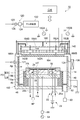
- FIG. 2 is a diagram illustrating an example of a plasma processing apparatus.
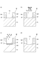
- 3 is a cross-sectional view showing a state of the object to be processed before and after execution of each step shown in FIG. 1, which includes (a) part, (b) part, (c) part, and (d) part. It is.
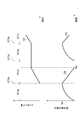
- FIG. 4 is a diagram showing a change in the etching amount with respect to the etching target layer and the thickness of the mixed layer formed in the etching target layer during the execution of the method shown in FIG.
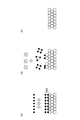
- FIG. 5 is a diagram showing the principle of etching in the method shown in FIG. 1, comprising (a) part, (b) part, and (c) part.
- FIG. 1 is a flow diagram illustrating an embodiment method (method MT).
- a method MT according to an embodiment shown in FIG. 1 is a method for processing an object to be processed (hereinafter also referred to as “wafer”).
- the method MT is an example of a method for etching a wafer.
- a series of steps can be performed using a single plasma processing apparatus (for example, the plasma processing apparatus 10 shown in FIG. 2).
- FIG. 2 is a schematic diagram illustrating the plasma processing apparatus 10 according to an embodiment.
- a plasma processing apparatus 10 shown in FIG. 2 includes an ICP (Inductively Coupled Plasma) type plasma source.
- the plasma processing apparatus 10 includes a processing container 192 formed in a cylindrical shape (for example, a cylindrical shape) made of metal (for example, aluminum).
- the processing container 192 defines a processing space Sp in which plasma processing is performed.
- the shape of the processing container 192 is not limited to a cylindrical shape. For example, a rectangular tube shape (for example, a box shape) may be used.
- the plasma source of the plasma processing apparatus 10 is not limited to the ICP type, and can be, for example, an ECR (Electron Cyclotron Resonance) type, a CCP (Capacitively Coupled Plasma) type, or a type using a microwave. .
- ECR Electro Cyclotron Resonance
- CCP Capacitively Coupled Plasma
- the mounting table PD includes an electrostatic chuck ESC and a lower electrode LE.
- the lower electrode LE includes a first plate 18a and a second plate 18b.
- the processing container 192 defines a processing space Sp.
- the support unit 14 is provided on the bottom of the processing container 192 inside the processing container 192.
- the support part 14 is provided with a substantially cylindrical shape, for example.
- the support part 14 is comprised from an insulating material, for example.
- the insulating material constituting the support portion 14 may contain oxygen like quartz.
- the support portion 14 extends in the vertical direction from the bottom of the processing container 192 in the processing container 192.
- the mounting table PD is provided in the processing container 192.
- the mounting table PD is supported by the support unit 14.
- the mounting table PD holds the wafer W on the upper surface of the mounting table PD.
- the wafer W is an object to be processed.
- the mounting table PD includes a lower electrode LE and an electrostatic chuck ESC.
- the lower electrode LE includes a first plate 18a and a second plate 18b.
- the first plate 18a and the second plate 18b are made of a metal such as aluminum, for example.
- the first plate 18a and the second plate 18b have, for example, a substantially disk shape.
- the second plate 18b is provided on the first plate 18a.
- the second plate 18b is electrically connected to the first plate 18a.
- the electrostatic chuck ESC is provided on the second plate 18b.
- the electrostatic chuck ESC has a structure in which conductive film electrodes are arranged between a pair of insulating layers or between a pair of insulating sheets.
- the DC power supply 22 is electrically connected to the electrode of the electrostatic chuck ESC via the switch 23.
- the electrostatic chuck ESC attracts the wafer W by an electrostatic force generated by a DC voltage from the DC power supply 22. As a result, the electrostatic chuck ESC can hold the wafer W.
- the focus ring FR is disposed on the peripheral edge of the second plate 18b so as to surround the edge of the wafer W and the electrostatic chuck ESC.
- the focus ring FR is provided in order to improve etching uniformity.
- the focus ring FR is made of a material appropriately selected according to the material of the film to be etched, and can be made of, for example, quartz.
- the coolant channel 24 is provided inside the second plate 18b.
- the refrigerant flow path 24 constitutes a temperature adjustment mechanism.
- Refrigerant is supplied to the refrigerant flow path 24 from a chiller unit provided outside the processing container 192 via a pipe 26a.
- the refrigerant supplied to the refrigerant flow path 24 is returned to the chiller unit via the pipe 26b.
- the refrigerant is supplied to the refrigerant flow path 24 so that the refrigerant circulates.
- the gas supply line 28 supplies the heat transfer gas from the heat transfer gas supply mechanism, for example, He gas, between the upper surface of the electrostatic chuck ESC and the back surface of the wafer W.
- the heater HT is a heating element.
- the heater HT is embedded in the second plate 18b.
- the heater power supply HP is connected to the heater HT. By supplying electric power from the heater power supply HP to the heater HT, the temperature of the mounting table PD is adjusted, and the temperature of the wafer W mounted on the mounting table PD is adjusted.
- the heater HT can be incorporated in the electrostatic chuck ESC.
- the plate-like dielectric 194 is disposed opposite the mounting table PD above the mounting table PD.
- the lower electrode LE and the plate-like dielectric 194 are provided substantially parallel to each other.
- a processing space Sp is provided between the plate-like dielectric 194 and the lower electrode LE.
- the processing space Sp is a space region for performing plasma processing on the wafer W.
- a deposition shield 46 is detachably provided along the inner wall of the processing container 192.
- the deposition shield 46 is also provided on the outer periphery of the support portion 14.
- the deposition shield 46 prevents the etching by-product (deposition) from adhering to the processing container 192, and can be configured by coating an aluminum material with ceramics such as Y 2 O 3 .
- the deposition shield can be made of a material containing oxygen such as quartz.
- the exhaust plate 48 is provided on the bottom side of the processing container 192 and between the support portion 14 and the side wall of the processing container 192.
- the exhaust plate 48 can be configured by, for example, coating an aluminum material with ceramics such as Y 2 O 3 .
- the exhaust port 12 e is provided in the processing container 192 below the exhaust plate 48.
- the exhaust device 50 is connected to the exhaust port 12 e via the exhaust pipe 52.
- the exhaust device 50 includes a vacuum pump such as a turbo molecular pump, and can reduce the pressure in the processing container 192 to a desired degree of vacuum.
- the high frequency power source 64 is a power source that generates a second high frequency power for drawing ions into the wafer W, that is, a high frequency bias power, and has a frequency within a range of 400 [kHz] to 40.68 [MHz]. A high frequency bias power of 13 [MHz] is generated.
- the high frequency power supply 64 is connected to the lower electrode LE via the matching unit 68.
- the matching unit 68 is a circuit for matching the output impedance of the high-frequency power source 64 with the input impedance on the load side (lower electrode LE side).
- a plate-like dielectric 194 made of, for example, quartz glass or ceramic is provided on the ceiling of the processing container 192 so as to face the mounting table PD. Specifically, the plate-like dielectric 194 is formed in a disk shape, for example, and is airtightly attached so as to close the opening formed in the ceiling portion of the processing container 192.
- the processing space Sp is a space where plasma is generated by the plasma source.
- the processing space Sp is a space where the wafer W is placed.
- the processing container 192 is provided with a gas supply unit 120 that supplies a first processing gas and a second processing gas described later.
- the gas supply unit 120 supplies the first processing gas and the second processing gas to the processing space Sp described above.
- a gas inlet 121 is formed in the side wall of the processing vessel 192, and a gas supply source 122 is connected to the gas inlet 121 via a gas supply pipe 123.
- a flow rate controller for example, a mass flow controller 124 and an opening / closing valve 126) for controlling the flow rates of the first processing gas and the second processing gas is interposed.
- the first process gas and the second process gas output from the gas supply source 122 are controlled by the mass flow controller 124 to have a preset flow rate, and the gas inlet 121.
- the mass flow controller 124 controls the mass flow controller 124 to have a preset flow rate, and the gas inlet 121.
- the gas supply unit 120 is expressed using a single gas line for the sake of simplicity.
- the gas supply unit 120 includes a plurality of gas types (at least the first processing gas and the first processing gas).
- the second processing gas is provided as a processing gas.
- the gas supply part 120 shown in FIG. 2 is provided with the structure which supplies gas from the side wall part of the processing container 192 as an example, the gas supply part 120 is not restricted to the structure shown in FIG.
- the gas supply unit 120 may be configured to supply gas from the ceiling of the processing container 192.
- a gas introduction port is formed in, for example, the central portion of the plate-like dielectric 194, and gas can be supplied from this gas introduction port.
- An exhaust device 50 that exhausts the atmosphere in the processing container 192 is connected to the bottom of the processing container 192 via an exhaust pipe 52.
- the exhaust device 50 is configured by, for example, a vacuum pump, and can set the pressure in the processing container 192 to a preset pressure.
- a wafer loading / unloading port 134 is provided on the side wall of the processing chamber 192, and a gate valve 136 is provided at the wafer loading / unloading port 134.
- the gate valve 136 is opened, and after the wafer W is mounted on the mounting table PD in the processing container 192 by a transfer mechanism such as a transfer arm (not shown), the gate valve 136 is set. The wafer W is closed and processing of the wafer W is started.
- a planar high-frequency antenna 140 and a shield member 160 that covers the high-frequency antenna 140 are provided on the upper surface (outer surface) of the plate-like dielectric 194 on the ceiling of the processing container 192.
- the high-frequency antenna 140 according to the embodiment includes an inner antenna element 142A disposed at the center of the plate-like dielectric 194 and an outer antenna element 142B disposed so as to surround the outer periphery of the inner antenna element 142A.
- Each of the inner antenna element 142A and the outer antenna element 142B is a conductor such as copper, aluminum, and stainless steel, and has a spiral coil shape.
- Both the inner antenna element 142A and the outer antenna element 142B are sandwiched and integrated with a plurality of sandwiching bodies 144.
- the sandwiching body 144 has, for example, a bar shape.
- the sandwiching body 144 is arranged in a radial pattern so as to project from the vicinity of the center of the inner antenna element 142A to the outside of the outer antenna element 142B.
- the shield member 160 includes an inner shield wall 162A and an outer shield wall 162B.
- the inner shield wall 162A is provided between the inner antenna element 142A and the outer antenna element 142B so as to surround the inner antenna element 142A.
- the outer shield wall 162B is provided so as to surround the outer antenna element 142B, and has a cylindrical shape. Therefore, the upper side surface of the plate-like dielectric 194 is divided into a central portion (central zone) inside the inner shield wall 162A and a peripheral portion (peripheral zone) between the inner shield wall 162A and the outer shield wall 162B. .
- a disc-shaped inner shield plate 164A is provided on the inner antenna element 142A so as to close the opening of the inner shield wall 162A.
- a donut-shaped outer shield plate 164B is provided so as to close an opening between the inner shield wall 162A and the outer shield wall 162B.
- the shape of the shield member 160 is not limited to a cylindrical shape.
- the shape of the shield member 160 can be, for example, another shape such as a rectangular tube shape, or can be adapted to the shape of the processing container 192.
- the processing container 192 has, for example, a substantially cylindrical shape
- the shield member 160 also has a substantially cylindrical shape in accordance with the cylindrical shape.
- the shield member 160 also has a substantially rectangular tube shape.
- the high frequency power supply 150A and the high frequency power supply 150B are separately connected to the inner antenna element 142A and the outer antenna element 142B, respectively. Thereby, high frequency of the same frequency or different frequency can be applied to each of the inner antenna element 142A and the outer antenna element 142B.
- a high frequency of, for example, 27 [MHz] is supplied from the high frequency power supply 150A to the inner antenna element 142A with a preset power [W]
- the processing container is caused by the induced magnetic field formed in the processing container 192.
- the processing gas introduced into 192 is excited, and a donut-shaped plasma can be generated at the center on the wafer W.
- the processing container when a high frequency of, for example, 27 [MHz] or the like is supplied from the high frequency power supply 150B to the outer antenna element 142B with a preset power [W], the processing container is caused by an induction magnetic field formed in the processing container 192. The processing gas introduced into 192 is excited, and another donut-shaped plasma can be generated at the peripheral edge on the wafer W.
- the high frequency output from each of the high frequency power supply 150A and the high frequency power supply 150B is not limited to the above-described frequency, and various high frequencies can be supplied from the high frequency power supply 150A and the high frequency power supply 150B.
- the electrical lengths of the inner antenna element 142A and the outer antenna element 142B need to be adjusted in accordance with the high frequency output from each of the high frequency power supply 150A and the high frequency power supply 150B.
- the height can be adjusted separately by the actuator 168A and the actuator 168B.
- the control unit Cnt is a computer including a processor, a storage unit, an input device, a display device, and the like, and controls each unit of the plasma processing apparatus 10. Specifically, the control unit Cnt is connected to the mass flow controller 124, the opening / closing valve 126, the exhaust device 50, the high frequency power source 150A, the high frequency power source 150B, the high frequency power source 64, the matching unit 68, the heater power source HP, and the chiller unit. .
- the control unit Cnt operates according to a program based on the input recipe and sends out a control signal.
- a control signal from the control unit Cnt at least the selection and flow rate of the gas supplied from the gas supply source 122, the exhaust of the exhaust device 50, and the power supply from the high frequency power supply 150A, the high frequency power supply 150B, and the high frequency power supply 64 It is possible to control the power supply of the heater power supply HP and the refrigerant flow rate and refrigerant temperature from the chiller unit.
- each process of the method (method MT shown in FIG. 1) for processing the target object disclosed in this specification can be executed by operating each part of the plasma processing apparatus 10 under the control of the control unit Cnt. .
- FIG. 3 is a cross-sectional view showing a state of the object to be processed before and after execution of each step shown in FIG. 1, which includes (a) part, (b) part, (c) part, and (d) part. It is.
- FIG. 4 is a diagram showing a change in the etching amount with respect to the etching target layer and the thickness of the mixed layer formed in the etching target layer during the execution of the method shown in FIG.
- FIG. 5 is a diagram showing the principle of etching in the method shown in FIG.
- step ST1 a wafer W shown in FIG. 3A is prepared, and the wafer W is accommodated in the processing container 192 of the plasma processing apparatus 10 and placed on the electrostatic chuck ESC.
- step ST1 the above-described wafer W shown in part (a) of FIG. 3 is prepared as the wafer W shown in FIG. 2, and then each step of sequence SQ and step ST3 is executed.
- a wafer W shown in part (a) of FIG. 3 is provided on a support base (not shown), a layer EL to be etched provided on the support base, and a layer EL to be etched (surface SF of the layer EL to be etched).
- a mask MK, and a trench TR provided in the mask MK.
- the trench TR extends from the surface of the mask MK to the surface SF of the etched layer EL, and exposes the etched layer EL. That is, a part of the surface SF of the layer to be etched EL is exposed through the trench TR.
- the material of the etched layer EL includes an oxide of silicon, and may include, for example, SiO 2 .
- the material of the mask MK can include, for example, TiN.
- a sequence SQ and a series of steps ST3 subsequent to the step ST1 are steps for etching the etching target layer EL.
- the sequence SQ is executed once (unit cycle) or more.
- the sequence SQ is a series of etching that precisely etches a region not covered by the mask MK in the layer to be etched EL with a high selection ratio regardless of the density of the mask MK by a method similar to the ALE (Atomic Layer Etching) method.
- Step ST2a first step
- step ST2b second step
- step ST2c third step
- step ST2d fourth step
- step ST2a plasma of the first processing gas is generated in the processing container 192 of the plasma processing apparatus 10 in which the wafer W is accommodated, and the mixed layer MX containing ions contained in the plasma of the first processing gas is formed. Then, it is formed in the atomic layer of the surface SF of the etched layer EL through the trench TR.
- a bias voltage is applied to the plasma of the first processing gas via the high-frequency power supply 64, and the first processing gas plasma is included in the atomic layer of the surface SF of the etched layer EL.
- a mixed layer MX containing ions may be formed.
- the first processing gas is supplied into the processing container 192, and the first The plasma of the processing gas is generated.
- the first processing gas includes nitrogen, and specifically may include N 2 gas.
- Black circles (black circles) shown in part (b) of FIG. 3 indicate ions (nitrogen atom ions) included in the plasma of the first gas.
- a first processing gas containing N 2 gas is supplied into the processing container 192 from a gas source selected from among a plurality of gas sources of the gas supply source 122.
- the high-frequency power is supplied from the high-frequency power supply 150A and the high-frequency power supply 150B, the high-frequency bias voltage is supplied from the high-frequency power supply 64, and the exhaust device 50 is operated to preset the atmospheric pressure of the processing space Sp in the processing container 192. Set to value.
- the plasma of the first processing gas is generated in the processing container 192, and ions (nitrogen atom ions) contained in the plasma of the first processing gas are attracted in the vertical direction by the high-frequency bias power.
- the surface SF of the etching target layer EL that is in contact with the surface SF of the etching target EL through the trench TR and is exposed through the trench TR is anisotropically modified.
- the anisotropically modified portion of the surface SF of the layer to be etched EL in the process ST2a becomes the mixed layer MX.
- the first gas is N 2 gas and the layer to be etched EL contains silicon oxide (for example, SiO 2 ), the composition of the mixed layer MX can be SiN / SiO 2 (SiON).
- FIG. 5 is a diagram showing the principle of etching in the method (sequence SQ) shown in FIG. 1, which includes the parts (a), (b), and (c).
- white circles (white circles) indicate atoms (for example, atoms constituting SiO 2 ) constituting the layer to be etched EL, and black circles (black circles) indicate the plasma of the first gas.
- the “x” surrounded by a circle indicates a radical contained in the plasma of the second gas described later.
- step ST2a ions of nitrogen atoms (black circles (black circles)) contained in the plasma of the first gas are transferred into the trench TR.
- the mixed layer MX including the atoms constituting the layer to be etched EL and the nitrogen atoms of the first gas is formed on the atomic layer of the surface SF of the layer to be etched EL exposed by the trench TR by the step ST2a. (See also (c) part of FIG. 3 together with (a) part of FIG. 5).
- step ST2a nitrogen atoms are supplied to the atomic layer (atomic layer of silicon oxide) on the surface SF of the etched layer EL, and silicon nitride A mixed layer MX (SiN / SiO 2 ) containing can be formed in the atomic layer of the surface SF.
- step ST2b the processing space Sp in the processing container 192 is purged. Specifically, the first processing gas supplied in step ST2a is exhausted.
- an inert gas such as a rare gas (eg, Ar gas) may be supplied to the processing container 192 as a purge gas. That is, the purge in the step ST2b may be either a gas purge for flowing an inert gas into the processing container 192 or a purge by evacuation.
- step ST2c subsequent to step ST2b, plasma of the second processing gas is generated in the processing container 192, and the mixed layer MX is removed by chemical etching using radicals contained in the plasma.
- step ST2c as shown in part (c) of FIG. 3, the wafer W after the formation of the mixed layer MX in step ST2a is placed on the electrostatic chuck ESC in the processing container 192.
- a second processing gas is supplied, and plasma of the second processing gas is generated.
- the plasma of the second processing gas generated in the step ST2c includes radicals that remove the mixed layer MX containing silicon nitride. “X” surrounded by a circle shown in part (c) of FIG. 3 indicates radicals contained in the plasma of the second gas.
- the second processing gas includes fluorine, and may be a mixed gas including, for example, NF 3 gas and O 2 gas.
- the second processing gas is also a mixed gas containing NF 3 gas, O 2 gas, H 2 gas, and Ar gas, and a mixed gas containing CH 3 F gas, O 2 gas, and Ar gas.
- the second processing gas is supplied into the processing container 192 from a gas source selected from the gas sources of the gas supply source 122, and high-frequency power is supplied from the high-frequency power source 150A and the high-frequency power source 150B.
- the atmospheric pressure of the processing space Sp in the processing container 192 is set to a preset value. In this manner, plasma of the second processing gas is generated in the processing container 192.
- the radicals in the plasma of the second processing gas generated in step ST2c come into contact with the mixed layer MX on the surface SF of the layer to be etched EL through the trench TR.
- the radical ST of the second process gas is supplied to the mixed layer MX formed on the surface SF of the etched layer EL by the process ST2c, and the mixed layer MX is chemically etched. Can be removed from the etched layer EL.
- the mixed layer MX formed on the surface SF of the etched layer EL is caused by radicals contained in the plasma of the second processing gas. It can be removed from the surface SF of the etched layer EL.
- step ST2d subsequent to step ST2c, the processing space Sp in the processing container 192 is purged. Specifically, the second processing gas supplied in step ST2c is exhausted.
- an inert gas such as a rare gas (eg, Ar gas) may be supplied to the processing container 192 as a purge gas.
- the purge in step ST2d may be either a gas purge for flowing an inert gas into the processing container 192 or a purge by evacuation.
- step ST3 it is determined whether or not to end the execution of the sequence SQ. Specifically, in step ST3, it is determined whether or not the number of executions of the sequence SQ has reached a preset number.
- the determination of the number of execution times of the sequence SQ is to determine the etching amount for the etching target layer EL (the depth of the groove formed in the etching target layer EL by etching).
- the sequence SQ can be repeatedly executed so that the etching target layer EL is etched until the etching amount with respect to the etching target layer EL reaches a preset value. As the number of executions of the sequence SQ increases, the etching amount for the etching target layer EL also increases (substantially linearly increases).
- the product of the thickness of the layer EL to be etched (the thickness of the mixed layer MX formed in one step ST2a) and the number of executions of the sequence SQ is determined in advance by executing the sequence SQ once (unit cycle).
- the number of executions of the sequence SQ can be determined so as to be a set value.
- a graph G1 in FIG. 4 shows a change in an etching amount (arbitrary unit) with respect to the etching target layer EL generated during the execution of the sequence SQ
- a graph G2 in FIG. 4 shows an etching target layer EL generated during the execution of the sequence SQ.
- the change of the thickness (arbitrary unit) of the mixed layer MX formed in FIG. The horizontal axis of FIG.
- the execution of the step ST2a is performed until the thickness of the mixed layer MX reaches a preset value TH as shown in the graph G2.
- the value TH of the thickness of the mixed layer MX formed in the step ST2a is the value of the bias power applied by the high frequency power supply 64 and the unit time of the ions contained in the plasma of the first gas with respect to the layer to be etched EL. Can be determined by the amount of dose and the execution time of the process ST2a.
- the execution of the step ST2c removes all the mixed layer MX formed in the step ST2a as shown in the graph G1 and the graph G2. It is done until it is done.
- the mixed layer MX is completely removed by chemical etching before the timing TM is reached during the execution of the process ST2b.
- the timing TM can be determined by the etching rate of chemical etching performed in step ST2c.
- the timing TM is generated during the execution of the process ST2b. Between the timing TM and the end of the process ST2b, the etched layer EL of the silicon oxide after the removal of the mixed layer MX is not etched by the plasma of the second processing gas (self-limited).
- the etching rate of etching with respect to silicon oxide (for example, SiO 2 ) constituting the etched layer EL is the nitridation of silicon contained in the mixed layer MX. Compared to the etching rate of etching with respect to an object (for example, SiN), it is extremely small.
- step ST3 When it is determined in step ST3 that the number of executions of the sequence SQ has not reached the preset number (step ST3: NO), the execution of the sequence SQ is repeated again. On the other hand, when it is determined in step ST3 that the number of executions of the sequence SQ has reached the preset number (step ST3: YES), the execution of the sequence SQ is ended.
- the sequence SQ and the series of steps ST3 are performed by repeatedly executing the sequence SQ using the mask MK to remove the layer to be etched EL for each atomic layer, thereby increasing the pattern density of the mask MK and the width of the trench TR. Regardless of (value), this is a step of precisely etching the layer to be etched EL.
- the sequence SQ is repeated a predetermined number of times, so that the layer to be etched EL is provided with the trench TR provided by the mask MK regardless of the pattern density of the mask MK and the width (value) of the trench TR.
- the layer to be etched EL can be removed for each atomic layer by a method similar to the ALE method.
- the first process for the etched layer EL is performed while maintaining a relatively large etching amount of silicon nitride relative to the silicon oxide in the etched layer EL. It has been found by the inventors that the amount of sputtering by gas plasma can be sufficiently reduced.
- the second processing gas may be a mixed gas of NF 3 gas, O 2 gas, H 2 gas, and Ar gas.
- the following process conditions can be used in step ST2c.
- the value [W] of the high frequency power of the high frequency power source 64 0 [W] (13 [MHz])
- Second processing gas mixed gas containing NF 3 gas and O 2 gas
- the ICP type plasma source has been described as an example.
- the plasma source of the plasma processing apparatus 10 is not limited to the ICP type, and a CCP type can also be used.
- examples of main process conditions of the process ST2a and the process ST2c when the plasma source of the plasma processing apparatus 10 is the CCP type will be described.
- ashing may be further performed under the following process conditions after step ST2c.
- Second processing gas O 2 gas Flow rate of second processing gas [sccm]: 750 [sccm] Processing time [s]: 60 [s]
- step ST2a of the sequence SQ that is repeatedly executed, first, nitrogen is contained with respect to the surface SF of the etched layer EL including the silicon oxide exposed through the trench TR of the mask MK.
- the mixed layer MX containing nitrogen ions is formed by the plasma of the first processing gas.
- the mixed layer MX contains silicon nitride.
- step ST2c of sequence SQ the silicon nitride mixed layer MX formed in step ST2a is removed using radicals contained in the plasma of the second processing gas containing fluorine.
- step ST2a in which the first gas containing nitrogen is used, the mixed layer MX containing silicon nitride is formed along the shape of the opening of the trench TR of the mask MK in detail, and the second layer containing fluorine.
- step ST2c in which a gas is used, the mixed layer MX is removed from the etched layer EL. Therefore, it is possible to etch the etched layer EL in a state where the shape of the opening of the trench TR of the mask MK is maintained in detail while avoiding the formation of deposits on the opening and side surfaces of the trench TR of the mask MK.
- the etched layer EL can be etched uniformly regardless of the width of the trench TR of the mask MK and the density of the pattern of the trench TR of the mask MK. Further, the sequence SQ including the steps ST2a and ST2c is repeatedly executed, so that the shape of the opening of the trench TR of the mask MK is maintained in detail, and the width of the trench TR and the mask MK of the mask MK are maintained.
- the layer to be etched EL can be etched uniformly to a desired depth regardless of the density of the trench TR pattern.
- SYMBOLS 10 Plasma processing apparatus, 120 ... Gas supply part, 121 ... Gas introduction port, 122 ... Gas supply source, 123 ... Gas supply piping, 124 ... Mass flow controller, 126 ... Open / close valve, 12e ... Exhaust port, 134 ... Wafer carry-in / out port DESCRIPTION OF SYMBOLS 136 ... Gate valve, 14 ... Support part, 140 ... High frequency antenna, 142A ... Inner antenna element, 142B ... Outer antenna element, 144 ... Holding body, 150A ... High frequency power source, 150B ... High frequency power source, 160 ... Shield member, 162A ... Inner shield wall, 162B ...
- outer shield wall 164A ... inner shield plate, 164B ... outer shield plate, 168A ... actuator, 168B ... actuator, 18a ... first plate, 18b ... second plate, 192 ... processing vessel, 194 ... plate Dielectric, 22 ... DC power supply, 23 ... switch, 4 ... refrigerant flow path, 26a ... piping, 26b ... piping, 28 ... gas supply line, 46 ... depot shield, 48 ... exhaust plate, 50 ... exhaust device, 52 ... exhaust pipe, 64 ... high frequency power supply, 68 ...
Landscapes
- Engineering & Computer Science (AREA)
- Physics & Mathematics (AREA)
- Plasma & Fusion (AREA)
- Chemical & Material Sciences (AREA)
- Condensed Matter Physics & Semiconductors (AREA)
- General Physics & Mathematics (AREA)
- Manufacturing & Machinery (AREA)
- Computer Hardware Design (AREA)
- Microelectronics & Electronic Packaging (AREA)
- Power Engineering (AREA)
- Analytical Chemistry (AREA)
- Chemical Kinetics & Catalysis (AREA)
- General Chemical & Material Sciences (AREA)
- Inorganic Chemistry (AREA)
- Electromagnetism (AREA)
- Spectroscopy & Molecular Physics (AREA)
- Drying Of Semiconductors (AREA)
- High Energy & Nuclear Physics (AREA)
- Plasma Technology (AREA)
- Health & Medical Sciences (AREA)
- Toxicology (AREA)
Abstract
一実施形態では、シリコンの酸化物を含む被エッチング層と被エッチング層上に設けられたマスクとマスクに設けられ被エッチング層を露出する溝とを備えた被処理体を処理する一実施形態に係る方法において、窒素を含む第1の処理ガスのプラズマを生成し該プラズマに含まれるイオンを含む混合層を被エッチング層の露出面の原子層に形成して、フッ素を含む第2の処理ガスのプラズマを生成し該プラズマに含まれるラジカルによって混合層を除去するシーケンスを繰り返し実行し、被エッチング層を原子層毎に除去することによって被エッチング層をエッチングする。第2の処理ガスのプラズマは、シリコンの窒化物を含む混合層を除去するラジカルを含む。
Description
本発明の実施形態は、被処理体を処理する方法に関するものである。
プラズマ処理装置を用いた被処理体のプラズマ処理の一種として、プラズマエッチングがある。プラズマエッチングに用いられるレジストマスクは、フォトリソグラフィ技術によって形成され、被エッチング層に形成されるパターンの限界寸法は、フォトリソグラフィ技術によって形成されるレジストマスクの解像度に依存する。しかし、レジストマスクの解像度には解像限界がある。電子デバイスの高集積化に対する要求が益々高まっており、レジストマスクの解像限界よりも小さい寸法のパターンを形成することが要求されるようになっている。このため、特許文献1に記載されているように、レジストマスク上にシリコン酸化膜を形成することによって、当該レジストマスクの寸法を調整し、当該レジストマスクによって提供される開口の幅を縮小する技術が提案されている。このため、特許文献1に記載されているように、レジストマスク上にシリコン酸化膜を形成することによって、当該レジストマスクの寸法を調整し、当該レジストマスクによって提供される開口の幅を縮小する技術が提案されている。
一方、近年の電子デバイスの高集積化に伴う微細化によって、被処理体上のパターン形成のうち積層構造に含まれる有機膜等に対するエッチングを進めて行く場合において、高精度の最小線幅(CD:Critical Dimension)の制御が要求される。従来では、10[nm]以下の細穴スリットをSiO2膜に垂直に設ける場合には、堆積性のCxFy系ガスを用いることによって、マスクとの選択比を得ている。しかしながら、CxFy系ガスに起因して生じる堆積物が細穴スリットの開口の閉塞を引き起こし得る。従って、CxFy系ガスを用いてSiO2膜に10[nm]以下の細穴スリットを形成する場合には、エッチング量(エッチングによって形成されるスリットの深さ)と選択比とのトレードオフが生じ得る。従って、シリコンの酸化物を含む被処理体に対するエッチングにおいて、マスクとの選択比を良好に維持しつつ細穴スリットを形成する技術が望まれている。
一態様においては、被処理体を処理する方法が提供される。被処理体は被エッチング層と該被エッチング層上に設けられたマスクと該マスクに設けられた溝(細穴スリット)とを備え、該溝は該マスクの表面から該被エッチング層に至り該被エッチング層を露出する。該方法は、被処理体が収容されているプラズマ処理装置の処理容器内において第1の処理ガスのプラズマを生成し、該第1の処理ガスのプラズマに含まれるイオンを含む混合層を、溝を介して被エッチング層の表面の原子層に形成する第1の工程と、第1の工程の実行後に、処理容器内の空間をパージする第2の工程と、第2の工程の実行後に、処理容器内において第2の処理ガスのプラズマを生成し、該第2の処理ガスのプラズマに含まれるラジカルによって混合層を除去する第3の工程と、第3の工程の実行後に、処理容器内の空間をパージする第4の工程と、を含むシーケンスを繰り返し実行し、被エッチング層を原子層毎に除去することによって、該被エッチング層をエッチングする。被エッチング層は、シリコンの酸化物を含み、第1の処理ガスは、窒素を含み、第2の処理ガスは、フッ素を含む。そして、第3の工程において生成される第2の処理ガスのプラズマは、シリコンの窒化物を含む混合層を除去するラジカルを含む。
上記方法において、繰返し実行されるシーケンスの第1の工程では、まず、マスクの溝を介して露出されたシリコンの酸化物を含む被エッチング層の表面に対して、窒素を含む第1の処理ガスのプラズマによって、窒素イオンを含有する混合層を形成する。この混合層は、シリコンの窒化物を含有することとなる。そして、当該シーケンスの第3の工程では、第1の工程で形成されたシリコンの窒化物の混合層がフッ素を含む第2の処理ガスのプラズマに含まれるラジカルを用いて除去される。このように、窒素を含む第1のガスが用いられる第1の工程においてシリコンの窒化物を含む混合層がマスクの溝の開口の形状に詳細に沿って形成され、フッ素を含む第2のガスが用いられる第3の工程において当該混合層が被エッチング層から除去される。従って、マスクの溝の開口および側面に対する堆積物の形成を回避しつつ、マスクの溝の開口の形状が詳細に維持された状態で被エッチング層に対するエッチングが可能となる。マスクの溝の幅やマスクの溝のパターンの疎密に依らず均一に、被エッチング層に対するエッチングが可能となる。更に、このような第1の工程および第3の工程を含むシーケンスが繰り返し実行されることによって、マスクの溝の開口の形状が詳細に維持された状態で、マスクの溝の幅やマスクの溝のパターンの疎密に依らず均一に、所望とする深さに至るまで被エッチング層に対するエッチングが可能となる。
一実施形態において、第1の工程では、第1の処理ガスのプラズマにバイアス電圧を印加して、被エッチング層の表面の原子層にイオンを含む混合層を形成し得る。このように、第1の処理ガスのプラズマにバイアス電圧が印可されるので、当該プラズマに含まれるイオン(窒素原子のイオン)がマスクの溝を介して露出された被エッチング層の表面に対して異方的に供給され得る。このため、被エッチング層の表面に形成される混合層は、溝の上から見て溝の開口の形状と高詳細に一致する形状に形成可能となる。
一実施形態において、第2の処理ガスは、NF3ガスおよびO2ガスを含む混合ガス、NF3ガス、O2ガス、H2ガスおよびArガスを含む混合ガス、または、CH3Fガス、O2ガスおよびArガスを含む混合ガスであり得る。このように、フッ素を含有する第2の処理ガスが実現され得る。
以上説明したように、シリコンの酸化物を含む被処理体に対するエッチングにおいて、マスクとの選択比を良好に維持しつつ細穴スリットを形成する技術が提供される。
以下、図面を参照して種々の実施形態について詳細に説明する。なお、各図面において同一または相当の部分に対しては同一の符号を附すこととする。以下、図1を参照して、プラズマ処理装置10を用いて実施することができるエッチング方法(方法MT)について説明する。図1は、一実施形態の方法(方法MT)を示す流れ図である。図1に示す一実施形態の方法MTは、被処理体(以下、「ウエハ」ということがある)を処理する方法である。方法MTは、ウエハをエッチングする方法の一例である。一実施形態の方法MTでは、一連の工程を単一のプラズマ処理装置(例えば、図2に示すプラズマ処理装置10)を用いて実行することが可能である。
図2は、一実施形態のプラズマ処理装置10を示す概要図である。図2に示すプラズマ処理装置10は、ICP(Inductively Coupled Plasma)型のプラズマ源を備える。プラズマ処理装置10は、金属製(例えばアルミニウム製)の筒状(例えば円筒状)に形成された処理容器192を備える。処理容器192は、プラズマ処理が行われる処理空間Spを画成する。なお、処理容器192の形状は円筒状に限られるものではない。例えば角筒状(例えば箱状)であってもよい。また、プラズマ処理装置10のプラズマ源は、ICP型に限るものではなく、例えば、ECR(Electron Cyclotron Resonance)型、CCP(Capacitively Coupled Plasma)型や、マイクロ波を用いたもの等であることができる。
処理容器192の底部には、ウエハWを載置するための載置台PDが設けられている。載置台PDは、静電チャックESC、下部電極LEを備える。下部電極LEは、第1プレート18a、第2プレート18bを備える。処理容器192は、処理空間Spを画成する。
支持部14は、処理容器192の内側において、処理容器192の底部上に設けられる。支持部14は、例えば、略円筒状の形状を備える。支持部14は、例えば、絶縁材料から構成される。支持部14を構成する絶縁材料は、石英のように酸素を含み得る。支持部14は、処理容器192内において、処理容器192の底部から鉛直方向に延在する。
載置台PDは、処理容器192内に設けられる。載置台PDは、支持部14によって支持される。載置台PDは、載置台PDの上面において、ウエハWを保持する。ウエハWは、被処理体である。載置台PDは、下部電極LEおよび静電チャックESCを備える。
下部電極LEは、第1プレート18aおよび第2プレート18bを含む。第1プレート18aおよび第2プレート18bは、例えばアルミニウム等の金属から構成される。第1プレート18aおよび第2プレート18bは、例えば、略円盤状の形状を備える。第2プレート18bは、第1プレート18a上に設けられる。第2プレート18bは、第1プレート18aに電気的に接続される。
静電チャックESCは、第2プレート18b上に設けられる。静電チャックESCは、一対の絶縁層の間、または、一対の絶縁シートの間において、導電膜の電極が配置された構造を備える。直流電源22は、スイッチ23を介して、静電チャックESCの電極に電気的に接続される。静電チャックESCは、直流電源22からの直流電圧によって生じる静電力によって、ウエハWを吸着する。これによって、静電チャックESCは、ウエハWを保持することができる。
フォーカスリングFRは、ウエハWのエッジおよび静電チャックESCを囲むように、第2プレート18bの周縁部上に配置される。フォーカスリングFRは、エッチングの均一性を向上させるために設けられる。フォーカスリングFRは、エッチング対象の膜の材料によって適宜選択される材料から構成されており、例えば、石英から構成され得る。
冷媒流路24は、第2プレート18bの内部に設けられる。冷媒流路24は、温調機構を構成する。冷媒流路24には、処理容器192の外部に設けられるチラーユニットから配管26aを介して冷媒が供給される。冷媒流路24に供給される冷媒は、配管26bを介してチラーユニットに戻される。このように、冷媒流路24には、冷媒が循環するように、供給される。この冷媒の温度を制御することによって、静電チャックESCによって支持されるウエハWの温度が制御される。ガス供給ライン28は、伝熱ガス供給機構からの伝熱ガス、例えばHeガスを、静電チャックESCの上面とウエハWの裏面との間に供給する。
ヒータHTは、加熱素子である。ヒータHTは、例えば、第2プレート18b内に埋め込まれる。ヒータ電源HPは、ヒータHTに接続される。ヒータ電源HPからヒータHTに電力が供給されることによって、載置台PDの温度が調整され、そして、載置台PD上に載置されるウエハWの温度が調整される。なお、ヒータHTは、静電チャックESCに内蔵され得る。
板状誘電体194は、載置台PDの上方において、載置台PDと対向配置される。下部電極LEと板状誘電体194とは、互いに略平行に設けられる。板状誘電体194と下部電極LEとの間には、処理空間Spが提供される。処理空間Spは、プラズマ処理をウエハWに行うための空間領域である。
プラズマ処理装置10では、処理容器192の内壁に沿ってデポシールド46が着脱自在に設けられている。デポシールド46は、支持部14の外周にも設けられている。デポシールド46は、処理容器192にエッチング副生物(デポ)が付着することを防止するものであり、アルミニウム材にY2O3等のセラミックスを被覆することにより構成され得る。デポシールドは、Y2O3の他に、例えば、石英のように酸素を含む材料から構成され得る。
排気プレート48は、処理容器192の底部側であって、且つ、支持部14と処理容器192の側壁との間に設けられている。排気プレート48は、例えば、アルミニウム材にY2O3等のセラミックスを被覆することによって構成され得る。排気口12eは、排気プレート48の下方において、処理容器192に設けられている。排気装置50は、排気管52を介して排気口12eに接続される。排気装置50は、ターボ分子ポンプ等の真空ポンプを備えており、処理容器192内の空間を所望の真空度まで減圧することができる。高周波電源64は、ウエハWにイオンを引き込むための第2の高周波電力、すなわち高周波バイアス電力を発生する電源であり、400[kHz]~40.68[MHz]の範囲内の周波数、一例においては13[MHz]の高周波バイアス電力を発生する。高周波電源64は、整合器68を介して下部電極LEに接続される。整合器68は、高周波電源64の出力インピーダンスと負荷側(下部電極LE側)の入力インピーダンスとを整合させるための回路である。
処理容器192の天井部には、例えば石英ガラスやセラミック等で構成された板状誘電体194が載置台PDに対向するように設けられている。具体的には、板状誘電体194は、例えば円板状に形成され、処理容器192の天井部に形成された開口を塞ぐように気密に取り付けられている。処理空間Spは、プラズマ源によってプラズマが生成される空間である。処理空間Spは、ウエハWが載置される空間である。
処理容器192には、後述の第1の処理ガスおよび第2の処理ガスを供給するガス供給部120が設けられている。ガス供給部120は、上述した処理空間Spへ、第1の処理ガスおよび第2の処理ガスを供給する。処理容器192の側壁部にはガス導入口121が形成されており、ガス導入口121にはガス供給配管123を介してガス供給源122が接続されている。ガス供給配管123の途中には第1の処理ガスおよび第2の処理ガスの流量を制御する流量制御器(例えば、マスフローコントローラ124、および、開閉バルブ126)が介在している。このようなガス供給部120によれば、ガス供給源122から出力される第1の処理ガスおよび第2の処理ガスは、マスフローコントローラ124によって予め設定された流量に制御されて、ガス導入口121から処理容器192の処理空間Spへ供給される。
なお、図2では説明を簡単にするため、ガス供給部120を一系統のガスラインを用いて表現しているが、ガス供給部120は、複数のガス種(少なくとも、第1の処理ガスおよび第2の処理ガス)を処理ガスとして供給する構成を備える。また、図2に示すガス供給部120は、一例として、処理容器192の側壁部からガスを供給する構成を備えているが、ガス供給部120は、図2に示す構成に限られない。例えば、ガス供給部120は、処理容器192の天井部からガスを供給する構成を備えることもできる。ガス供給部120がこのような構成を備える場合には、例えば、板状誘電体194の例えば中央部にガス導入口が形成され、このガス導入口からガスが供給され得る。
処理容器192の底部には、処理容器192内の雰囲気を排出する排気装置50が排気管52を介して接続されている。排気装置50は、例えば真空ポンプによって構成され、処理容器192内の圧力を予め設定された圧力にし得る。
処理容器192の側壁部にはウエハ搬出入口134が設けられており、ウエハ搬出入口134にはゲートバルブ136が設けられている。例えばウエハWが搬入される際には、ゲートバルブ136が開かれ、図示しない搬送アーム等の搬送機構によってウエハWが処理容器192内の載置台PD上に載置された後に、ゲートバルブ136が閉じられて、ウエハWの処理が開始される。
処理容器192の天井部には、板状誘電体194の上側面(外側面)に、平面状の高周波アンテナ140と、高周波アンテナ140を覆うシールド部材160とが設けられる。一実施形態における高周波アンテナ140は、板状誘電体194の中央部に配置されている内側アンテナ素子142Aと、内側アンテナ素子142Aの外周を囲むように配置されている外側アンテナ素子142Bとを備える。内側アンテナ素子142A、外側アンテナ素子142Bのそれぞれは、例えば、銅、アルミニウム、ステンレス等の導体であり、渦巻きコイル状の形状を備える。
内側アンテナ素子142A、外側アンテナ素子142Bは、共に、複数の挟持体144に挟持されて一体となっている。挟持体144は、例えば、棒状の形状を備えている。挟持体144は、内側アンテナ素子142Aの中央付近から外側アンテナ素子142Bの外側に張り出すように放射線状に配置されている。
シールド部材160は、内側シールド壁162Aと外側シールド壁162Bとを備える。内側シールド壁162Aは、内側アンテナ素子142Aを囲むように、内側アンテナ素子142Aと外側アンテナ素子142Bとの間に設けられている。外側シールド壁162Bは、外側アンテナ素子142Bを囲むように設けられており、筒状の形状を備える。従って、板状誘電体194の上側面は、内側シールド壁162Aの内側の中央部(中央ゾーン)と、内側シールド壁162Aと外側シールド壁162Bとの間の周縁部(周縁ゾーン)とに分けられる。
内側アンテナ素子142A上には、内側シールド壁162Aの開口を塞ぐように円板状の内側シールド板164Aが設けられている。外側アンテナ素子142B上には、内側シールド壁162Aと外側シールド壁162Bとの間の開口を塞ぐようにドーナツ板状の外側シールド板164Bが設けられている。
シールド部材160の形状は、円筒状に限られるものではない。シールド部材160の形状は、例えば、角筒状等の他の形状であることができ、または、処理容器192の形状に合わせられたものであることができる。ここでは、処理容器192が例えば略円筒状の形状を備えるので、当該円筒形状に合わせてシールド部材160も略円筒状の形状を備える。処理容器192が略角筒状の形状を備えている場合には、シールド部材160も略角筒状の形状を備える。
内側アンテナ素子142A、外側アンテナ素子142Bのそれぞれには、高周波電源150A、高周波電源150Bのそれぞれが別々に接続されている。これにより、内側アンテナ素子142A、外側アンテナ素子142Bのそれぞれには、同じ周波数または異なる周波数の高周波を印加できる。例えば、高周波電源150Aから例えば27[MHz]等の周波数の高周波が予め設定されたパワー[W]で内側アンテナ素子142Aに供給されると、処理容器192内に形成された誘導磁界によって、処理容器192内に導入された処理ガスが励起され、ウエハW上の中央部にドーナツ型のプラズマが生成され得る。また、高周波電源150Bから例えば27[MHz]等の周波数の高周波が予め設定されたパワー[W]で外側アンテナ素子142Bに供給されると、処理容器192内に形成された誘導磁界によって、処理容器192内に導入された処理ガスが励起され、ウエハW上の周縁部に別のドーナツ型のプラズマが生成され得る。高周波電源150A、高周波電源150Bのそれぞれから出力される高周波は、上述した周波数に限られるものではなく、様々な周波数の高周波が、高周波電源150A、高周波電源150Bのそれぞれから供給され得る。なお、高周波電源150A、高周波電源150Bのそれぞれから出力される高周波に応じて、内側アンテナ素子142A、外側アンテナ素子142Bの電気的長さを調整する必要がある。内側シールド板164A、外側シールド板164Bのそれぞれでは、アクチュエータ168A、アクチュエータ168Bによって別々に高さが調整できる。
制御部Cntは、プロセッサ、記憶部、入力装置、表示装置等を備えるコンピュータであり、プラズマ処理装置10の各部を制御する。具体的に、制御部Cntは、マスフローコントローラ124、開閉バルブ126、排気装置50、高周波電源150A、高周波電源150B、高周波電源64、整合器68、ヒータ電源HP、および、チラーユニットに接続されている。
制御部Cntは、入力されたレシピに基づくプログラムに従って動作し、制御信号を送出する。制御部Cntからの制御信号によって、少なくとも、ガス供給源122から供給されるガスの選択および流量と、排気装置50の排気と、高周波電源150A、高周波電源150B、および、高周波電源64からの電力供給と、ヒータ電源HPの電力供給と、チラーユニットからの冷媒流量および冷媒温度とを制御することが可能である。なお、本明細書において開示される被処理体を処理する方法(図1に示す方法MT)の各工程は、制御部Cntによる制御によってプラズマ処理装置10の各部を動作させることによって、実行され得る。
図1に戻って、方法MTについての説明を続ける。以下の説明では、図1と共に、図2、図3、図4、図5を参照して説明する。図3は、(a)部、(b)部、(c)部、および、(d)部を備え、図1に示す各工程の実行前および実行後の被処理体の状態を示す断面図である。図4は、図1に示す方法の実行中における、被エッチング層に対するエッチング量と被エッチング層に形成される混合層の厚みとの変化を示す図である。図5は、図1に示す方法におけるエッチングの原理を示す図である。
工程ST1では、図3の(a)部に示すウエハWが準備され、ウエハWがプラズマ処理装置10の処理容器192内に収容され、静電チャックESC上に載置される。工程ST1において図2に示すウエハWとして図3の(a)部に示す上記のウエハWを準備した後に、シーケンスSQおよび工程ST3の各工程を実行する。図3の(a)部に示すウエハWは、図示しない支持基体と、この支持基体上に設けられた被エッチング層ELと、被エッチング層EL上(被エッチング層ELの表面SF)に設けられたマスクMKと、マスクMKに設けられた溝TRとを備える。溝TRは、マスクMKの表面から被エッチング層ELの表面SFに至り、被エッチング層ELを露出している。すなわち、被エッチング層ELの表面SFの一部は、溝TRを介して、露出されている。被エッチング層ELの材料は、シリコンの酸化物を含んでおり、例えば、SiO2を含み得る。マスクMKの材料は、例えばTiN等を含み得る。
工程ST1に引き続くシーケンスSQおよび工程ST3の一連の工程は、被エッチング層ELをエッチングする工程である。まず、工程ST1に引き続きシーケンスSQを一回(単位サイクル)以上実行する。シーケンスSQは、ALE(Atomic Layer Etching)法と同様の方法によって、被エッチング層ELのうちマスクMKで覆われていない領域を、マスクMKの疎密によらず高選択比で精密にエッチングする一連の工程であり、シーケンスSQにおいて順次実行される工程ST2a(第1の工程)、工程ST2b(第2の工程)、工程ST2c(第3の工程)、工程ST2d(第4の工程)を含む。
工程ST2aは、ウエハWが収容されているプラズマ処理装置10の処理容器192内において第1の処理ガスのプラズマを生成し、該第1の処理ガスのプラズマに含まれるイオンを含む混合層MXを、溝TRを介して被エッチング層ELの表面SFの原子層に形成する。例えば、工程ST2aでは、第1の処理ガスのプラズマに高周波電源64を介してバイアス電圧を印加して、被エッチング層ELの表面SFの原子層に対し、第1の処理ガスのプラズマに含まれるイオンを含む混合層MXを形成し得る。工程ST2aにおいて、図3の(b)部に示すように、ウエハWが静電チャックESC上に載置されている状態で、処理容器192内に第1の処理ガスを供給し、当該第1の処理ガスのプラズマを生成する。第1の処理ガスは、窒素を含み、具体的にはN2ガスを含み得る。図3の(b)部に示す黒塗りの円(黒丸)は、第1のガスのプラズマに含まれるイオン(窒素原子のイオン)を示している。具体的には、ガス供給源122の複数のガスソースのうち選択したガスソースからN2ガスを含む第1の処理ガスを処理容器192内に供給する。そして、高周波電源150Aおよび高周波電源150Bから高周波電力を供給し、高周波電源64から高周波バイアス電圧を供給し、排気装置50を動作させることによって処理容器192内の処理空間Spの気圧を予め設定された値に設定する。このようにして、第1の処理ガスのプラズマが処理容器192内において生成され、第1の処理ガスのプラズマに含まれるイオン(窒素原子のイオン)が、高周波バイアス電力による鉛直方向への引き込みよって、溝TRを介して被エッチング層ELの表面SFに接触し、溝TRを介して露出されている被エッチング層ELの表面SFが異方的に改質される。このように工程ST2aにおいて被エッチング層ELの表面SFのうち異方的に改質された箇所が、混合層MXとなる。第1のガスがN2ガスであり被エッチング層ELがシリコンの酸化物(例えばSiO2)を含むので、混合層MXの組成は、SiN/SiO2(SiON)であり得る。
図5は、(a)部、(b)部、および、(c)部を備え、図1に示す方法(シーケンスSQ)におけるエッチングの原理を示す図である。図5において、白抜きの円(白丸)は、被エッチング層ELを構成する原子(例えばSiO2を構成する原子)を示しており、黒塗りの円(黒丸)は、第1のガスのプラズマに含まれるイオン(窒素原子のイオン)を示しており、円で囲まれた「×」は、後述の第2のガスのプラズマに含まれるラジカルを示している。図5の(a)部および図3の(b)部に示すように、工程ST2aによって、第1のガスのプラズマに含まれる窒素原子のイオン(黒塗りの円(黒丸))が、溝TRを介して被エッチング層ELの表面SFの原子層に異方的に供給される。このように、工程ST2aによって、被エッチング層ELを構成する原子と第1のガスの窒素原子とを含む混合層MXが、溝TRによって露出されている被エッチング層ELの表面SFの原子層に形成される(図5の(a)部と共に図3の(c)部も参照)。
以上のように、第1のガスがN2ガスを含むので、工程ST2aにおいて、被エッチング層ELの表面SFの原子層(シリコンの酸化物の原子層)に窒素原子が供給され、シリコンの窒化物を含有する混合層MX(SiN/SiO2)が表面SFの原子層に形成され得る。
工程ST2aに引き続く工程ST2bでは、処理容器192内の処理空間Spをパージする。具体的には、工程ST2aにおいて供給された第1の処理ガスが排気される。工程ST2bでは、パージガスとして希ガス(例えばArガス等)といった不活性ガスを処理容器192に供給してもよい。すなわち、工程ST2bのパージは、不活性ガスを処理容器192内に流すガスパージ、または真空引きによるパージの何れであってもよい。
工程ST2bに引き続く工程ST2cでは、処理容器192内において第2の処理ガスのプラズマを生成し、該プラズマに含まれるラジカルを用いたケミカルエッチングによって、混合層MXを除去する。工程ST2cにおいて、図3の(c)部に示すように、工程ST2aにおいて混合層MXが形成された後のウエハWが静電チャックESC上に載置されている状態で、処理容器192内に第2の処理ガスを供給し、第2の処理ガスのプラズマを生成する。工程ST2cにおいて生成される第2の処理ガスのプラズマは、シリコンの窒化物を含む混合層MXを除去するラジカルを含む。図3の(c)部に示す円で囲まれた「×」は、第2のガスのプラズマに含まれるラジカルを示している。第2の処理ガスは、フッ素を含み、例えば、NF3ガスおよびO2ガスを含む混合ガスであり得る。なお、第2の処理ガスは、NF3ガス、O2ガス、H2ガス、および、Arガスを含む混合ガスや、CH3Fガス、O2ガス、および、Arガスを含む混合ガスでもあり得る。具体的には、ガス供給源122の複数のガスソースのうち選択したガスソースから上記の第2の処理ガスが処理容器192内に供給され、高周波電源150Aおよび高周波電源150Bから高周波電力が供給され、排気装置50を動作させることによって処理容器192内の処理空間Spの気圧が予め設定された値に設定される。このようにして、第2の処理ガスのプラズマが処理容器192内において生成される。工程ST2cにおいて生成された第2の処理ガスのプラズマ中のラジカルは、溝TRを介して被エッチング層ELの表面SFの混合層MXに接触する。図5の(b)部に示すように、工程ST2cによって、被エッチング層ELの表面SFに形成された混合層MXに第2の処理ガスの原子のラジカルが供給されて混合層MXがケミカルエッチングによって被エッチング層ELから除去され得る。
以上のように、図3の(d)部に示すように、工程ST2cにおいて、被エッチング層ELの表面SFに形成された混合層MXは、第2の処理ガスのプラズマに含まれるラジカルによって、被エッチング層ELの表面SFから除去され得る。
工程ST2cに引き続く工程ST2dでは、処理容器192内の処理空間Spをパージする。具体的には、工程ST2cにおいて供給された第2の処理ガスが排気される。工程ST2dでは、パージガスとして希ガス(例えばArガス等)といった不活性ガスを処理容器192に供給してもよい。すなわち、工程ST2dのパージは、不活性ガスを処理容器192内に流すガスパージ、または真空引きによるパージの何れであってもよい。
シーケンスSQに引き続く工程ST3では、シーケンスSQの実行を終了するか否かを判定する。具体的には、工程ST3では、シーケンスSQの実行回数が予め設定された回数に達したか否かを判定する。シーケンスSQの実行回数の決定は、被エッチング層ELに対するエッチング量(エッチングによって被エッチング層ELに形成される溝の深さ)を決定することである。シーケンスSQは、被エッチング層ELに対するエッチング量が予め設定された値に至るまで被エッチング層ELがエッチングされるように、繰り返し実行され得る。シーケンスSQの実行回数の増加に伴って、被エッチング層ELに対するエッチング量も増加(ほぼ線形的に増加)する。従って、1回(単位サイクル)のシーケンスSQの実行によってエッチングされる被エッチング層ELの厚み(1回の工程ST2aで形成される混合層MXの厚み)とシーケンスSQの実行回数との積が予め設定された値となるように、シーケンスSQの実行回数が決定され得る。
図4を参照して、シーケンスSQの実行中において生じる被エッチング層ELに対するエッチング量の変化と被エッチング層ELに形成される混合層MXの厚みの変化とについて説明する。図4のグラフG1は、シーケンスSQの実行中において生じる被エッチング層ELに対するエッチング量(任意単位)の変化を示しており、図4のグラフG2は、シーケンスSQの実行中において生じる被エッチング層ELに形成される混合層MXの厚み(任意単位)の変化を示している。図4の横軸は、シーケンスSQの実行中の時間を表しているが、工程ST2bの実行時間および工程ST2dの実行時間は図示簡略化のために省略されている。図4に示すように、1回(単位サイクル)のシーケンスSQの実行において、工程ST2aの実行は、グラフG2に示すように、混合層MXの厚みが予め設定された値THになるまで行われる。工程ST2aにおいて形成される混合層MXの厚みの値THは、高周波電源64によって印加されるバイアス電力の値と、第1のガスのプラズマに含まれているイオンの被エッチング層ELに対する単位時間当たりのドーズ(dose)量と、工程ST2aの実行時間とによって決定され得る。
また、図4に示すように、1回(単位サイクル)のシーケンスSQの実行において、工程ST2cの実行は、グラフG1およびグラフG2に示すように、工程ST2aで形成された混合層MXが全て除去されるまで行われる。工程ST2bの実行中においてタイミングTMに至るまでに、混合層MXがケミカルエッチングによって全て除去される。タイミングTMは、工程ST2cにおいて行われるケミカルエッチングのエッチングレートによって決定され得る。タイミングTMは、工程ST2bの実行中に生じる。タイミングTMから工程ST2bの終了までの間において、混合層MXの除去後におけるシリコンの酸化物の被エッチング層ELは、第2の処理ガスのプラズマによってはエッチングされない(セルフ・リミテッド)。すなわち、第2の処理ガスのプラズマに含まれるラジカルを用いた場合、被エッチング層ELを構成するシリコンの酸化物(例えばSiO2)に対するエッチングのエッチングレートは、混合層MXに含まれるシリコンの窒化物(例えばSiN)に対するエッチングのエッチングレートに比較して極めて小さい。
工程ST3においてシーケンスSQの実行回数が予め設定された回数に達していないと判定される場合には(工程ST3:NO)、シーケンスSQの実行が再び繰り返される。一方、工程ST3においてシーケンスSQの実行回数が予め設定された回数に達していると判定される場合には(工程ST3:YES)、シーケンスSQの実行が終了される。シーケンスSQおよび工程ST3の一連の工程は、マスクMKを用いてシーケンスSQを繰り返し実行して被エッチング層ELを原子層毎に除去することによって、マスクMKのパターンの粗密や溝TRの幅の程度(値)によらずに、被エッチング層ELを精密にエッチングする工程である。すなわち、シーケンスSQが予め設定された回数だけ繰り返されることによって、被エッチング層ELが、マスクMKのパターンの粗密や溝TRの幅の程度(値)によらずに、マスクMKが提供する溝TRの幅と同一および均一な幅で詳細にエッチングされ、また、マスクMKに対する選択比も向上される。以上のように、シーケンスSQおよび工程ST3の一連の工程は、ALE法と同様の方法によって、被エッチング層ELを原子層毎に除去することができる。
以下、工程ST2a、工程ST2cのそれぞれの主なプロセス条件の実施例を示す。
<工程ST2a>
・処理容器192内の圧力[mTorr]:30[mTorr]
・高周波電源150Aおよび高周波電源150Bの高周波電力の値[W]:0[W](27[MHz])
・高周波電源64の高周波電力の値[W]:0~200[W](13[MHz])
・第1の処理ガス:N2ガス
・第1の処理ガスの流量[sccm]:500[sccm]
・処理時間[s]:10~60[s]
高周波電源64の高周波電力の値は、20~100[W]が好適であり得る。高周波電源64の高周波電力の値がこの範囲にある場合、被エッチング層ELにおいてシリコンの酸化物に対するシリコンの窒化物のエッチング量を比較的に多く維持しつつ、被エッチング層ELに対する第1の処理ガスのプラズマによるスパッタ量を十分に低減し得ることが発明者によって見出された。
<工程ST2c>
・処理容器192内の圧力[mTorr]:50~400[mTorr]
・高周波電源150Aおよび高周波電源150Bの高周波電力の値[W]:0~800[W](27[MHz])
・高周波電源64の高周波電力の値[W]:0[W](13[MHz])
・第2の処理ガス:NF3ガスおよびO2ガスを含む混合ガス
・第2の処理ガスの流量[sccm]:120[sccm](NF3ガス)、40[sccm](O2ガス)
・処理時間[s]:10~50[s]
なお、処理容器192内の圧力が高いほど、シリコンの酸化物に対するシリコンの窒化物のエッチング量(選択比)が多く(高く)なり、さらに、エッチングによって混合層MXが全て除去された後には、工程ST2cを継続しても被エッチング層ELに対するエッチング量が少なくなる、という現象が発明者によって見出された。
また、工程ST2cにおいて、第2の処理ガスは、NF3ガス、O2ガス、H2ガスおよびArガスの混合ガスであり得る。この第2の処理ガスを用いた場合、工程ST2cでは、以下のプロセス条件が利用され得る。
・処理容器192内の圧力[mTorr]:350[mTorr]
・高周波電源150Aおよび高周波電源150Bの高周波電力の値[W]:200[W](27[MHz])
・高周波電源64の高周波電力の値[W]:0[W](13[MHz])
・第2の処理ガス:NF3ガスおよびO2ガスを含む混合ガス
・第2の処理ガスの流量[sccm]:45[sccm](NF3ガス)、300[sccm](O2ガス)、40[sccm](H2ガス)、100[sccm](Arガス)
・処理時間[s]:10[s]
・処理容器192内の圧力[mTorr]:350[mTorr]
・高周波電源150Aおよび高周波電源150Bの高周波電力の値[W]:200[W](27[MHz])
・高周波電源64の高周波電力の値[W]:0[W](13[MHz])
・第2の処理ガス:NF3ガスおよびO2ガスを含む混合ガス
・第2の処理ガスの流量[sccm]:45[sccm](NF3ガス)、300[sccm](O2ガス)、40[sccm](H2ガス)、100[sccm](Arガス)
・処理時間[s]:10[s]
<シーケンスSQ>
・繰り返し回数:20~50回
なお、シーケンスSQの繰り返し回数が多いほど、被エッチング層ELに対するエッチング量も多くなる。
・繰り返し回数:20~50回
なお、シーケンスSQの繰り返し回数が多いほど、被エッチング層ELに対するエッチング量も多くなる。
上記した一実施形態に係るプラズマ処理装置10では、ICP型のプラズマ源を例示して説明したが、プラズマ処理装置10のプラズマ源としてはICP型に限らず、CCP型も用い得る。以下、プラズマ処理装置10のプラズマ源がCCP型の場合における工程ST2a、工程ST2cのそれぞれの主なプロセス条件の実施例を示す。
<工程ST2a>
・処理容器192内の圧力[mTorr]:10[mTorr]
・処理容器192の天井部に設けられる高周波電源の高周波電力の値[W]:500[W](60[MHz])
・高周波電源64の高周波電力の値[W]:100[W](13[MHz])
・第1の処理ガス:N2ガス
・第1の処理ガスの流量[sccm]:500[sccm]
・処理時間[s]:60[s]
<工程ST2c>
・処理容器192内の圧力[mTorr]:50[mTorr]
・処理容器192の天井部に設けられる高周波電源の高周波電力の値[W]:1000[W](60[MHz])
・高周波電源64の高周波電力の値[W]:0~100[W](13[MHz])
・第2の処理ガス:CH3Fガス、O2ガスおよびArガスを含む混合ガス
・第2の処理ガスの流量[sccm]:25[sccm](CH3Fガス)、20[sccm](O2ガス)、700[sccm](Arガス)
・処理時間[s]:60[s]
エッチングによって混合層MXが全て除去された後には、工程ST2cを継続しても被エッチング層ELに対するエッチング量は少ない。なお、シーケンスSQにおいて、工程ST2cの後に下記のプロセス条件でアッシング処理を更に行う場合がある。
<アッシング処理>
・処理容器192内の圧力[mTorr]:100[mTorr]
・処理容器192の天井部に設けられる高周波電源の高周波電力の値[W]:600[W](60[MHz])
・高周波電源64の高周波電力の値[W]:0[W](13[MHz])
・第2の処理ガス:O2ガス
・第2の処理ガスの流量[sccm]:750[sccm]
・処理時間[s]:60[s]
<アッシング処理>
・処理容器192内の圧力[mTorr]:100[mTorr]
・処理容器192の天井部に設けられる高周波電源の高周波電力の値[W]:600[W](60[MHz])
・高周波電源64の高周波電力の値[W]:0[W](13[MHz])
・第2の処理ガス:O2ガス
・第2の処理ガスの流量[sccm]:750[sccm]
・処理時間[s]:60[s]
上記の方法MTにおいて、繰返し実行されるシーケンスSQの工程ST2aでは、まず、マスクMKの溝TRを介して露出されたシリコンの酸化物を含む被エッチング層ELの表面SFに対して、窒素を含む第1の処理ガスのプラズマによって、窒素イオンを含有する混合層MXを形成する。混合層MXは、シリコンの窒化物を含有することとなる。そして、シーケンスSQの工程ST2cでは、工程ST2aで形成されたシリコンの窒化物の混合層MXがフッ素を含む第2の処理ガスのプラズマに含まれるラジカルを用いて除去される。このように、窒素を含む第1のガスが用いられる工程ST2aにおいてシリコンの窒化物を含む混合層MXがマスクMKの溝TRの開口の形状に詳細に沿って形成され、フッ素を含む第2のガスが用いられる工程ST2cにおいて混合層MXが被エッチング層ELから除去される。従って、マスクMKの溝TRの開口および側面に対する堆積物の形成を回避しつつ、マスクMKの溝TRの開口の形状が詳細に維持された状態で被エッチング層ELに対するエッチングが可能となる。マスクMKの溝TRの幅やマスクMKの溝TRのパターンの疎密に依らず均一に、被エッチング層ELに対するエッチングが可能となる。更に、このような工程ST2aおよび工程ST2cを含むシーケンスSQが繰り返し実行されることによって、マスクMKの溝TRの開口の形状が詳細に維持された状態で、マスクMKの溝TRの幅やマスクMKの溝TRのパターンの疎密に依らず均一に、所望とする深さに至るまで被エッチング層ELに対するエッチングが可能となる。
さらに、第1の処理ガスのプラズマにバイアス電圧が印可される場合には、当該プラズマに含まれるイオン(窒素原子のイオン)がマスクMKの溝TRを介して露出された被エッチング層ELの表面SFに対して異方的に供給され得る。このため、被エッチング層ELの表面SFに形成される混合層MXは、溝TRの上から見て溝TRの開口の形状と高詳細に一致する形状に形成可能となる。
以上、好適な実施の形態において本発明の原理を図示し説明してきたが、本発明は、そのような原理から逸脱することなく配置および詳細において変更され得ることは、当業者によって認識される。本発明は、本実施の形態に開示された特定の構成に限定されるものではない。従って、特許請求の範囲およびその精神の範囲から来る全ての修正および変更に権利を請求する。
10…プラズマ処理装置、120…ガス供給部、121…ガス導入口、122…ガス供給源、123…ガス供給配管、124…マスフローコントローラ、126…開閉バルブ、12e…排気口、134…ウエハ搬出入口、136…ゲートバルブ、14…支持部、140…高周波アンテナ、142A…内側アンテナ素子、142B…外側アンテナ素子、144…挟持体、150A…高周波電源、150B…高周波電源、160…シールド部材、162A…内側シールド壁、162B…外側シールド壁、164A…内側シールド板、164B…外側シールド板、168A…アクチュエータ、168B…アクチュエータ、18a…第1プレート、18b…第2プレート、192…処理容器、194…板状誘電体、22…直流電源、23…スイッチ、24…冷媒流路、26a…配管、26b…配管、28…ガス供給ライン、46…デポシールド、48…排気プレート、50…排気装置、52…排気管、64…高周波電源、68…整合器、Cnt…制御部、EL…被エッチング層、ESC…静電チャック、FR…フォーカスリング、G1…グラフ、G2…グラフ、HP…ヒータ電源、HT…ヒータ、LE…下部電極、MK…マスク、MT…方法、MX…混合層、PD…載置台、SF…表面、Sp…処理空間、SQ…シーケンス、TH…値、TM…タイミング、TR…溝、W…ウエハ。
Claims (5)
- 被処理体を処理する方法であって、該被処理体は被エッチング層と該被エッチング層上に設けられたマスクと該マスクに設けられた溝とを備え、該溝は該マスクの表面から該被エッチング層に至り該被エッチング層を露出し、該方法は、
前記被処理体が収容されているプラズマ処理装置の処理容器内において第1の処理ガスのプラズマを生成し、該第1の処理ガスのプラズマに含まれるイオンを含む混合層を、前記溝を介して前記被エッチング層の表面の原子層に形成する第1の工程と、
前記第1の工程の実行後に、前記処理容器内の空間をパージする第2の工程と、
前記第2の工程の実行後に、前記処理容器内において第2の処理ガスのプラズマを生成し、該第2の処理ガスのプラズマに含まれるラジカルによって前記混合層を除去する第3の工程と、
前記第3の工程の実行後に、前記処理容器内の空間をパージする第4の工程と、
を含むシーケンスを繰り返し実行し、前記被エッチング層を原子層毎に除去することによって、該被エッチング層をエッチングし、
前記被エッチング層は、シリコンの酸化物を含み、
前記第1の処理ガスは、窒素を含み、
前記第2の処理ガスは、フッ素を含み、
前記第3の工程において生成される前記第2の処理ガスのプラズマは、シリコンの窒化物を含む前記混合層を除去する前記ラジカルを含む、
方法。 - 前記第1の工程では、前記第1の処理ガスのプラズマにバイアス電圧を印加して、前記被エッチング層の表面の原子層に前記イオンを含む前記混合層を形成する、
請求項1に記載の方法。 - 前記第2の処理ガスは、NF3ガスおよびO2ガスを含む混合ガスである、
請求項1または請求項2に記載の方法。 - 前記第2の処理ガスは、NF3ガス、O2ガス、H2ガスおよびArガスを含む混合ガスである、
請求項1または請求項2に記載の方法。 - 前記第2の処理ガスは、CH3Fガス、O2ガスおよびArガスを含む混合ガスである、
請求項1または請求項2に記載の方法。
Priority Applications (5)
| Application Number | Priority Date | Filing Date | Title |
|---|---|---|---|
| KR1020237028539A KR20230127373A (ko) | 2016-11-07 | 2017-11-02 | 피처리체를 처리하는 방법 |
| KR1020197013091A KR102571380B1 (ko) | 2016-11-07 | 2017-11-02 | 피처리체를 처리하는 방법 |
| US16/347,697 US11081360B2 (en) | 2016-11-07 | 2017-11-02 | Method for processing workpiece |
| CN201780068805.1A CN109923648B (zh) | 2016-11-07 | 2017-11-02 | 处理被处理体的方法 |
| US17/362,285 US20210327719A1 (en) | 2016-11-07 | 2021-06-29 | Method for processing workpiece |
Applications Claiming Priority (2)
| Application Number | Priority Date | Filing Date | Title |
|---|---|---|---|
| JP2016217163A JP6763750B2 (ja) | 2016-11-07 | 2016-11-07 | 被処理体を処理する方法 |
| JP2016-217163 | 2016-11-07 |
Related Child Applications (2)
| Application Number | Title | Priority Date | Filing Date |
|---|---|---|---|
| US16/347,697 A-371-Of-International US11081360B2 (en) | 2016-11-07 | 2017-11-02 | Method for processing workpiece |
| US17/362,285 Continuation US20210327719A1 (en) | 2016-11-07 | 2021-06-29 | Method for processing workpiece |
Publications (1)
| Publication Number | Publication Date |
|---|---|
| WO2018084255A1 true WO2018084255A1 (ja) | 2018-05-11 |
Family
ID=62076951
Family Applications (1)
| Application Number | Title | Priority Date | Filing Date |
|---|---|---|---|
| PCT/JP2017/039772 WO2018084255A1 (ja) | 2016-11-07 | 2017-11-02 | 被処理体を処理する方法 |
Country Status (6)
| Country | Link |
|---|---|
| US (2) | US11081360B2 (ja) |
| JP (1) | JP6763750B2 (ja) |
| KR (2) | KR20230127373A (ja) |
| CN (1) | CN109923648B (ja) |
| TW (1) | TWI759348B (ja) |
| WO (1) | WO2018084255A1 (ja) |
Families Citing this family (2)
| Publication number | Priority date | Publication date | Assignee | Title |
|---|---|---|---|---|
| JP7066565B2 (ja) * | 2018-07-27 | 2022-05-13 | 東京エレクトロン株式会社 | プラズマ処理方法およびプラズマ処理装置 |
| US10950428B1 (en) * | 2019-08-30 | 2021-03-16 | Mattson Technology, Inc. | Method for processing a workpiece |
Citations (3)
| Publication number | Priority date | Publication date | Assignee | Title |
|---|---|---|---|---|
| JP2001210627A (ja) * | 1999-11-16 | 2001-08-03 | Matsushita Electric Ind Co Ltd | エッチング方法、半導体装置及びその製造方法 |
| JP2016015382A (ja) * | 2014-07-01 | 2016-01-28 | 東京エレクトロン株式会社 | エッチング方法、エッチング装置及び記憶媒体 |
| JP2016127285A (ja) * | 2015-01-06 | 2016-07-11 | ラム リサーチ コーポレーションLam Research Corporation | 活性化を使用しない、シリコン酸化物のための異方性原子層エッチング |
Family Cites Families (13)
| Publication number | Priority date | Publication date | Assignee | Title |
|---|---|---|---|---|
| US5571366A (en) * | 1993-10-20 | 1996-11-05 | Tokyo Electron Limited | Plasma processing apparatus |
| US5786276A (en) * | 1997-03-31 | 1998-07-28 | Applied Materials, Inc. | Selective plasma etching of silicon nitride in presence of silicon or silicon oxides using mixture of CH3F or CH2F2 and CF4 and O2 |
| US5942446A (en) * | 1997-09-12 | 1999-08-24 | Taiwan Semiconductor Manufacturing Company, Ltd. | Fluorocarbon polymer layer deposition predominant pre-etch plasma etch method for forming patterned silicon containing dielectric layer |
| KR100480610B1 (ko) | 2002-08-09 | 2005-03-31 | 삼성전자주식회사 | 실리콘 산화막을 이용한 미세 패턴 형성방법 |
| JP2013258244A (ja) * | 2012-06-12 | 2013-12-26 | Tokyo Electron Ltd | エッチング方法及びプラズマ処理装置 |
| JP5982223B2 (ja) * | 2012-08-27 | 2016-08-31 | 東京エレクトロン株式会社 | プラズマ処理方法、及びプラズマ処理装置 |
| US8956980B1 (en) * | 2013-09-16 | 2015-02-17 | Applied Materials, Inc. | Selective etch of silicon nitride |
| JP2015084396A (ja) * | 2013-09-19 | 2015-04-30 | 東京エレクトロン株式会社 | エッチング方法 |
| JP6277004B2 (ja) * | 2014-01-31 | 2018-02-07 | 株式会社日立ハイテクノロジーズ | ドライエッチング方法 |
| US9548303B2 (en) * | 2014-03-13 | 2017-01-17 | Taiwan Semiconductor Manufacturing Company, Ltd. | FinFET devices with unique fin shape and the fabrication thereof |
| US9142459B1 (en) * | 2014-06-30 | 2015-09-22 | Applied Materials, Inc. | Wafer dicing using hybrid laser scribing and plasma etch approach with mask application by vacuum lamination |
| JP6366454B2 (ja) * | 2014-10-07 | 2018-08-01 | 東京エレクトロン株式会社 | 被処理体を処理する方法 |
| JP6339963B2 (ja) * | 2015-04-06 | 2018-06-06 | 東京エレクトロン株式会社 | エッチング方法 |
-
2016
- 2016-11-07 JP JP2016217163A patent/JP6763750B2/ja active Active
-
2017
- 2017-10-31 TW TW106137484A patent/TWI759348B/zh active
- 2017-11-02 WO PCT/JP2017/039772 patent/WO2018084255A1/ja active Application Filing
- 2017-11-02 KR KR1020237028539A patent/KR20230127373A/ko not_active Application Discontinuation
- 2017-11-02 US US16/347,697 patent/US11081360B2/en active Active
- 2017-11-02 CN CN201780068805.1A patent/CN109923648B/zh active Active
- 2017-11-02 KR KR1020197013091A patent/KR102571380B1/ko active IP Right Grant
-
2021
- 2021-06-29 US US17/362,285 patent/US20210327719A1/en active Pending
Patent Citations (3)
| Publication number | Priority date | Publication date | Assignee | Title |
|---|---|---|---|---|
| JP2001210627A (ja) * | 1999-11-16 | 2001-08-03 | Matsushita Electric Ind Co Ltd | エッチング方法、半導体装置及びその製造方法 |
| JP2016015382A (ja) * | 2014-07-01 | 2016-01-28 | 東京エレクトロン株式会社 | エッチング方法、エッチング装置及び記憶媒体 |
| JP2016127285A (ja) * | 2015-01-06 | 2016-07-11 | ラム リサーチ コーポレーションLam Research Corporation | 活性化を使用しない、シリコン酸化物のための異方性原子層エッチング |
Also Published As
| Publication number | Publication date |
|---|---|
| CN109923648B (zh) | 2023-06-23 |
| US20210327719A1 (en) | 2021-10-21 |
| US11081360B2 (en) | 2021-08-03 |
| US20190259627A1 (en) | 2019-08-22 |
| KR20230127373A (ko) | 2023-08-31 |
| JP6763750B2 (ja) | 2020-09-30 |
| KR20190075952A (ko) | 2019-07-01 |
| CN109923648A (zh) | 2019-06-21 |
| TWI759348B (zh) | 2022-04-01 |
| TW201829835A (zh) | 2018-08-16 |
| JP2018078138A (ja) | 2018-05-17 |
| KR102571380B1 (ko) | 2023-08-25 |
Similar Documents
| Publication | Publication Date | Title |
|---|---|---|
| US11380551B2 (en) | Method of processing target object | |
| US11145518B2 (en) | Method and apparatus for etching target object | |
| US20200185238A1 (en) | Apparatus for selectively etching first region made of silicon nitride against second region made of silicon oxide | |
| US9911607B2 (en) | Method of processing target object | |
| US11462412B2 (en) | Etching method | |
| KR20230129345A (ko) | 플라즈마 처리 장치 및 에칭 방법 | |
| US20210327719A1 (en) | Method for processing workpiece | |
| JP2019186501A (ja) | エッチングする方法及びプラズマ処理装置 | |
| CN109075068B (zh) | 蚀刻方法 |
Legal Events
| Date | Code | Title | Description |
|---|---|---|---|
| 121 | Ep: the epo has been informed by wipo that ep was designated in this application |
Ref document number: 17867438 Country of ref document: EP Kind code of ref document: A1 |
|
| ENP | Entry into the national phase |
Ref document number: 20197013091 Country of ref document: KR Kind code of ref document: A |
|
| NENP | Non-entry into the national phase |
Ref country code: DE |
|
| 122 | Ep: pct application non-entry in european phase |
Ref document number: 17867438 Country of ref document: EP Kind code of ref document: A1 |