WO2018083741A1 - レーザ照射装置 - Google Patents
レーザ照射装置 Download PDFInfo
- Publication number
- WO2018083741A1 WO2018083741A1 PCT/JP2016/082483 JP2016082483W WO2018083741A1 WO 2018083741 A1 WO2018083741 A1 WO 2018083741A1 JP 2016082483 W JP2016082483 W JP 2016082483W WO 2018083741 A1 WO2018083741 A1 WO 2018083741A1
- Authority
- WO
- WIPO (PCT)
- Prior art keywords
- laser
- spot diameter
- power
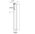
- throughput
- power consumption
- Prior art date
- Legal status (The legal status is an assumption and is not a legal conclusion. Google has not performed a legal analysis and makes no representation as to the accuracy of the status listed.)
- Ceased
Links
Images






Classifications
-
- B—PERFORMING OPERATIONS; TRANSPORTING
- B23—MACHINE TOOLS; METAL-WORKING NOT OTHERWISE PROVIDED FOR
- B23K—SOLDERING OR UNSOLDERING; WELDING; CLADDING OR PLATING BY SOLDERING OR WELDING; CUTTING BY APPLYING HEAT LOCALLY, e.g. FLAME CUTTING; WORKING BY LASER BEAM
- B23K26/00—Working by laser beam, e.g. welding, cutting or boring
-
- H—ELECTRICITY
- H01—ELECTRIC ELEMENTS
- H01S—DEVICES USING THE PROCESS OF LIGHT AMPLIFICATION BY STIMULATED EMISSION OF RADIATION [LASER] TO AMPLIFY OR GENERATE LIGHT; DEVICES USING STIMULATED EMISSION OF ELECTROMAGNETIC RADIATION IN WAVE RANGES OTHER THAN OPTICAL
- H01S3/00—Lasers, i.e. devices using stimulated emission of electromagnetic radiation in the infrared, visible or ultraviolet wave range
-
- H—ELECTRICITY
- H01—ELECTRIC ELEMENTS
- H01S—DEVICES USING THE PROCESS OF LIGHT AMPLIFICATION BY STIMULATED EMISSION OF RADIATION [LASER] TO AMPLIFY OR GENERATE LIGHT; DEVICES USING STIMULATED EMISSION OF ELECTROMAGNETIC RADIATION IN WAVE RANGES OTHER THAN OPTICAL
- H01S3/00—Lasers, i.e. devices using stimulated emission of electromagnetic radiation in the infrared, visible or ultraviolet wave range
- H01S3/10—Controlling the intensity, frequency, phase, polarisation or direction of the emitted radiation, e.g. switching, gating, modulating or demodulating
-
- H—ELECTRICITY
- H05—ELECTRIC TECHNIQUES NOT OTHERWISE PROVIDED FOR
- H05K—PRINTED CIRCUITS; CASINGS OR CONSTRUCTIONAL DETAILS OF ELECTRIC APPARATUS; MANUFACTURE OF ASSEMBLAGES OF ELECTRICAL COMPONENTS
- H05K3/00—Apparatus or processes for manufacturing printed circuits
- H05K3/10—Apparatus or processes for manufacturing printed circuits in which conductive material is applied to the insulating support in such a manner as to form the desired conductive pattern
Definitions
- This specification discloses a laser irradiation apparatus.
- Patent Document 1 a laser irradiation apparatus that performs baking by irradiating a conductive paste applied on a substrate with a laser.
- This device changes the spot diameter according to the line width of the conductive paste and also changes the output (power) of the laser light source in accordance with the change of the spot diameter, so that the energy (power) per unit area regardless of the spot diameter.
- the laser is irradiated so that the density is equal.
- the productivity increases as the throughput (processing capacity per unit time) increases, but the power consumption increases too much and the power cost may increase.
- the smaller the power consumption the lower the power cost, but the throughput may be lowered and the productivity may be lowered.
- the laser irradiation apparatus has been made to solve the above-described problem, and has a main purpose to enable setting of laser irradiation conditions that achieve an appropriate balance between both throughput and power consumption. To do.
- the laser irradiation apparatus of the present disclosure is A laser irradiation apparatus for irradiating a target portion of a substrate with a laser, A head having a laser light source; A stage on which the substrate is placed; A vertical movement device capable of adjusting the laser spot diameter irradiated to the target portion of the substrate by relatively moving the stage and the head in the vertical direction; In accordance with each of a plurality of adjustable laser spot diameters, a throughput and power consumption when irradiating a laser beam over the entire portion of the substrate to be processed are obtained, and the throughput and the power consumption are displayed in association with each other.
- the vertical movement device adjusts the diameter of the laser spot irradiated to the processing target portion of the substrate by relatively moving the stage and the head in the vertical direction.
- the control device obtains the throughput and power consumption when irradiating the laser over the entire processing target portion of the base material in accordance with each of a plurality of adjustable laser spot diameters.
- the control device displays the throughput and power consumption derived according to each of the plurality of laser spot diameters in association with each other on the display device. Thereby, the operator can select a well-balanced one from the correspondence relationship between the throughput displayed on the display device and the power consumption. As a result, it is possible to set the laser irradiation conditions so that both throughput and power consumption are in an appropriate balance.
- the part to be processed may be a part that needs a baking process, a part that needs a surface treatment, or a part that needs a heat curing process or a light curing process.
- a numerical value may be displayed or a graph may be displayed.
- FIG. 1 is a configuration diagram showing an outline of the configuration of a wiring substrate manufacturing apparatus 10.
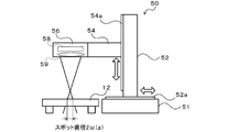
- FIG. FIG. 2 is a configuration diagram showing an outline of a configuration of a laser irradiation apparatus 50.
- FIG. 3 is an explanatory diagram showing an electrical connection relationship of the control device 70.
- Explanatory drawing which shows the mode of wiring layer formation.
- Explanatory drawing which shows the mode of wiring layer formation.
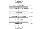
- the flowchart which shows an example of a baking process.
- Explanatory drawing which shows the relationship between spot diameter 2omega (z) and defocus distance z.
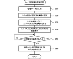
- the flowchart which shows an example of a laser irradiation condition setting process.
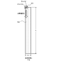
- Explanatory drawing which shows the relationship between the laser spot 60 and the conductive pattern 62.
- FIG. 5 is an explanatory diagram showing a correspondence relationship between throughput and power consumption displayed on a display.
- FIG. 1 is a configuration diagram showing an outline of the configuration of the wiring substrate manufacturing apparatus 10
- FIG. 2 is a configuration diagram showing an outline of the configuration of the laser irradiation apparatus 50
- FIG. 3 is an electrical diagram of the control apparatus 70. It is explanatory drawing which shows a proper connection relationship. Note that the front-rear direction in FIG. 1 is the X-axis direction, the left-right direction is the Y-axis direction, and the up-down direction is the Z-axis direction.
- the wiring substrate manufacturing apparatus 10 includes a stage 12, a transport device 20, a resin layer forming unit 30, a wiring layer forming unit 40, and a control device 70 (see FIG. 3).
- the resin layer forming unit 30 and the wiring layer forming unit 40 are arranged side by side along the transport direction (Y-axis direction) of the stage 12.
- the stage 12 is a work table used when the resin layer forming unit 30 and the wiring layer forming unit 40 perform work.
- the transport device 20 includes a pair of Y-axis guide rails 22 extending in the Y-axis direction, and a belt drive device 24 (see FIG. 3) that drives the timing belt, and transmits the timing belt.
- the stage 12 is reciprocated along the Y-axis guide rail 22 by the motive power.
- the resin layer forming unit 30 is for forming a resin layer on the stage 12 when the stage 12 is transported into the work area of the resin layer forming unit 30.
- the resin layer forming unit 30 includes an ink head 32 that can eject UV curable resin ink, and a UV light irradiation device that can irradiate the resin ink discharged from the ink head 32 with UV light. 34.
- the ink head 32 is, for example, a line head in which a plurality of nozzles are arranged so as to cover the entire width of the print area on the stage 12 (length in the X-axis direction).
- the ink head 32 applies (prints) a rectangular resin layer by discharging resin ink from the nozzles while conveying the stage 12 in the Y-axis direction by the conveying device 20.
- the UV light irradiation device 34 is configured to be able to irradiate linear UV light in the X-axis direction.
- the UV light irradiation device 34 is applied by irradiating the rectangular resin layer applied to the stage 12 with line-shaped (X-axis direction) UV light while transporting the stage 12 in the Y-axis direction.
- the cured resin layers are sequentially cured.
- a mercury lamp or a metal halide lamp can be used as the UV light irradiation device 34.
- the resin layer forming unit 30 thus repeats the application of the resin layer by the ink head 32 and the curing of the resin layer by the UV light irradiation device 34 a plurality of times, thereby laminating the resin layers, and having a predetermined thickness. A resin base material is produced.
- the wiring layer forming unit 40 is for forming a wiring layer on a resin base material formed on the stage 12 when the stage 12 is transported into the work area of the wiring layer forming unit 40.
- the wiring layer forming unit 40 includes an ink head 42 capable of discharging conductive particle-containing ink in which conductive particles such as metal nanoparticles are dispersed in a dispersant, and conductive particle-containing ink discharged from the ink head 42.
- the laser irradiation apparatus 50 of this embodiment which irradiates a laser beam is provided.
- the ink head 42 is, for example, a line head in which a plurality of nozzles are arranged so as to cover the entire width of the printing area.
- the ink head 42 applies (prints) the conductive particle-containing ink onto the base material by discharging the conductive particle-containing ink from the corresponding nozzle while the stage 12 is transported in the Y-axis direction by the transport device 20.
- a pattern to which conductive particle-containing ink is applied is referred to as a conductive pattern.
- the laser irradiation apparatus 50 of the present embodiment includes an X-axis slider 52 that can move in the X-axis direction, a Z-axis slider 54 that can move in the Z-axis direction, and a Z-axis slider 54. And a laser head 56 attached to the head.
- the laser head 56 incorporates a laser light source (laser oscillator) 58 that irradiates a laser beam in a spot shape in the Z-axis direction via the optical system 59.
- a laser light source laser oscillator
- the maximum value of the power P is 300 [W]
- the power resolution R p is 3 [W] (1% of full scale)
- the wavelength ⁇ is 1062 [nm]
- at the focal point at the focal point.
- the spot diameter 2 ⁇ 0 is 22 [ ⁇ m] ( ⁇ 0 is a spot radius).
- the conductive particle-containing ink applied on the substrate is made conductive by heating and decomposing the dispersing agent around the conductive particles by the laser irradiated by the laser light source 58.
- the conductive pattern made conductive by laser irradiation is referred to as wiring.
- the X-axis slider 52 moves along an X-axis guide rail 52a (see FIG. 2) provided on the pedestal 51, and the Z-axis slider 54 is moved along a Z-axis guide rail 54a (see FIG. 2) provided on the X-axis slider 52. ).
- the X-axis slider 52 is driven by an X-axis actuator 53 (see FIG. 3), and the Z-axis slider 54 is driven by a Z-axis actuator 55 (see FIG. 3).
- the laser head 56 attached to the Z-axis slider 54 can move in the X-axis direction and the Z-axis direction.
- the stage 12 is movable in the Y-axis direction along the Y-axis guide rail 22.
- the laser light source 58 can move to any position (X-axis direction and Y-axis) on the stage 12 (base material) by moving the laser head 56 in the X-axis direction and Z-axis direction and moving the stage 12 in the Y-axis direction. It is possible to irradiate a laser at an arbitrary height (position in the Z-axis direction).
- the laser irradiation device 50 moves the laser head 56 in the Z-axis direction to change the distance between the laser head 56 (laser light source 58) and the stage 12, thereby increasing the laser irradiation height.
- the spot diameter 2 ⁇ (z) is the smallest when the position of the laser head 56 in the Z-axis direction is at a position where the optical system 59 is in focus, and the spot diameter 2 ⁇ (z) becomes larger as the distance from the spot increases.
- the wiring layer forming unit 40 repeats the application of the conductive particle-containing ink by the ink head 42 and the conduction (firing) of the conductive particle-containing ink by the laser irradiation device 50 a plurality of times. Lamination is performed to form wiring on the resin substrate.
- the control device 70 includes a CPU 71, a ROM 72, a HDD 73, a RAM 74, and an input / output interface 75 as shown in FIG. These are electrically connected via a bus 76.
- Various detection signals from a position detection sensor for detecting each position of the stage 12 and the laser head 56 (laser light source 58) are input to the control device 70 via the input / output interface 75.
- the control device 70 outputs various control signals to the belt driving device 24, the ink head 32, the UV light irradiation device 34, the ink head 42, the laser light source 58, the X-axis actuator 53, the Z-axis actuator 55, the display 80, and the like. It is output via the input / output interface 75.
- FIG. 4 and FIG. 5 are explanatory diagrams showing the state of wiring layer formation.
- the wiring layer is formed by repeating discharge (printing) of conductive particle-containing ink and laser irradiation (firing) as described above.
- the stage 12 on which the resin base material is placed is moved in the Y-axis direction along the Y-axis guide rail 22 and the conductive particle-containing ink is ejected from the corresponding nozzle of the ink head 42 according to the wiring pattern. (See FIG. 4).
- the laser head 56 on which the laser light source 58 is mounted is moved in the X-axis direction in accordance with the wiring pattern while the laser light source 58 is irradiated with the laser downward. This is performed by moving the stage 12 in the Y-axis direction (see FIG. 5).
- FIG. 6 is a flowchart illustrating an example of the baking process. This process is performed after the conductive particles-containing ink is applied on the substrate by the ink head 42 to form a conductive pattern.
- the CPU 71 of the control device 70 When starting the firing process, the CPU 71 of the control device 70 first sets a defocus distance z that is a distance from the focal point of the optical system 59 (S110). In setting the defocus distance z, a preset spot diameter 2 ⁇ (z) is read. The spot diameter 2 ⁇ (z) is set based on the laser irradiation condition input by the operator. This point will be described later. If the shape of the laser beam is regarded as a hyperbola as shown in FIG. 7, the defocus distance z from the focal point and the spot radius ⁇ (z) satisfy the relationship of Expression (1). The wavelength ⁇ and the spot radius ⁇ 0 at the focal point are constants determined by the specifications of the laser irradiation apparatus 50 as described above. Therefore, if the spot radius ⁇ (z) is determined, the defocus distance z from the focal point is calculated from the equation (1).
- the CPU 71 drives and controls the Z-axis actuator 55 so as to obtain the set defocus distance z, and moves the laser head 56 in the Z-axis direction (S120). Subsequently, the CPU 71 sets the power P of the laser light source 58 (S130). Here, the power P is set so that the power density F of the laser spot is within the required power density range D p ⁇ ⁇ .
- the required power density range D p ⁇ ⁇ indicates an upper limit value D p + ⁇ and a lower limit value D p ⁇ of the power density required for firing the conductive particle-containing ink applied on the substrate (resin). It is determined by the thermal conductivity of the substrate, the thickness of the conductive particle-containing ink applied to the substrate, the decomposition temperature of the dispersant contained in the conductive particle-containing ink, and the like.
- the power density F of the laser spot irradiated from the laser light source 58 is below the lower limit value D p - ⁇ of the required power density, the firing of the conductive particle-containing ink becomes insufficient.
- the CPU 71 sets the power P so as to satisfy the formula (2).
- the power P is finally set in consideration of the power resolution R p corresponding to the minimum unit (one scale) when setting the power P.
- the CPU 71 drives and controls the belt driving device 24 and the X-axis actuator 53 to move the laser head 56 to the irradiation start position of the laser spot (S140). Then, the CPU 71 drives and controls the laser light source 58 so that the laser is irradiated with the power P set in S130 (S150), and the belt is driven so that the laser is scanned over the entire conductive pattern at a preset scanning speed V.
- the device 24 and the X-axis actuator 53 are driven and controlled (S160), and the firing process is terminated.
- the scanning speed V is set to a speed that allows the upper and lower limit width 2 ⁇ of the required power density range to be as wide as possible.
- FIG. 8 is a flowchart illustrating an example of laser irradiation condition setting processing. This process is performed before the baking process.
- the CPU 71 of the control device 70 When starting the laser irradiation condition setting process, the CPU 71 of the control device 70 first inputs various data (S210). Examples of the various data include the required power density range D p ⁇ ⁇ , the scanning speed V, the wavelength ⁇ , the maximum value of the power P, the power resolution R p , and the like.
- the required power density range D p ⁇ ⁇ is as described above. Here, it is assumed that 150 ⁇ 15 [W / mm 2 ] is input as the required power density range D p ⁇ ⁇ .
- the upper limit value D p + ⁇ of the required power density range is 165 [W / mm 2 ]
- the lower limit value D p - ⁇ is 135 [W / mm 2 ]
- the upper and lower limit width 2 ⁇ is 30 [W / Mm 2 ].
- 100 [mm / s] is input as the scanning speed V.
- 1062 [nm], 300 [W], and 3 [W] are input as the maximum value of the wavelength ⁇ and the power P and the power resolution R p , respectively.
- the CPU 71 obtains a settable range of the spot diameter 2 ⁇ (z) (S220). Specifically, a lower limit value and an upper limit value of the spot diameter 2 ⁇ (z) are calculated. First, calculation of the lower limit value will be described.
- the power density resolution R F is a value obtained by dividing the power resolution R P by the laser spot area. If the power density resolution R F is within the upper and lower limit widths 2 ⁇ of the required power density range (that is, the expression (4) is satisfied), the power density capable of firing the conductive particle-containing ink can be set without fail. From the formulas (3) and (4), the spot diameter 2 ⁇ (z) is 0.357 [mm] or more. Therefore, the CPU 71 sets the lower limit value of the spot diameter 2 ⁇ (z) to 0.357 [mm].
- R F R P / ⁇ 2 (z) (3)
- R F ⁇ 2 ⁇ 30 (4)
- the power P for setting the power density F to the upper limit value 165 [W / mm 2 ] of the required power density range is calculated by the equation (5). .5 [W].
- the power density F at this time is determined by the equation (5), it is 150 [W / mm 2 ], which falls within the required power density range.
- P ⁇ 2 (z) ⁇ F (5)
- the maximum spot diameter 2 ⁇ (z) at which the conductive pattern can be laser-fired is 135 [W / mm 2 ] which is the lower limit value as the power density F and 300 [W] which is the maximum value as the power P in Equation (5). Is calculated as 1.68 [mm]. Therefore, the CPU 71 sets the upper limit value of the spot diameter 2 ⁇ (z) to 1.68 [mm]. From the above, the settable range of the spot diameter 2 ⁇ (z) is set to 0.357 [mm] or more and 1.68 [mm] or less.
- the CPU 71 calculates throughput and power consumption according to the spot diameter 2 ⁇ (z) (step S230).
- the throughput is a firing processing capacity per unit time, and is a function of the spot diameter 2 ⁇ (z), and is a parameter that increases as the spot diameter 2 ⁇ (z) increases.
- the throughput is directly proportional to the spot diameter 2 ⁇ (z).
- the power consumption E is expressed by the product of the power P [W] and the irradiation time T [sec] as shown in Equation (6).
- the irradiation time T includes the length L [mm] in the longitudinal direction of the conductive pattern 62 shown in FIGS. 9 to 11, the effective spot diameter 2 ⁇ e (z) of the laser spot 60, the scanning speed V [mm / s], and the number of scans n. From [times], it can be obtained from equation (7).
- the effective spot diameter 2 ⁇ e (z) is represented by the product of the spot diameter 2 ⁇ (z) and the effective spot diameter ratio.
- the effective spot diameter ratio is a ratio indicating how much of the spot diameter 2 ⁇ (z) is an effective spot diameter that can be fired.
- n is an integer obtained by rounding up the fractional length of the value obtained by dividing the short direction length w [mm] of the conductive pattern 62 by the effective spot diameter 2 ⁇ e (z).
- E PT (6)
- T ⁇ (L ⁇ 2 ⁇ e (z)) / V ⁇ ⁇ n (7)
- the length L in the longitudinal direction and the length w in the short direction of the conductive pattern 62 are 5 [mm] and 0.6 [mm], respectively, and the effective spot diameter ratio is 0.5 (50%).
- the maximum value of the power P is 300 [W]
- the scanning speed V is 100 [mm / s]
- the lower limit value of the power density F is 135 [W / mm 2 ]
- the upper limit value is 165 [W].
- the lower limit of the spot diameter 2 ⁇ (z) is 0.357 [mm]
- the upper limit is 1.68 [mm].
- the scanning time n is halved and the irradiation time T is halved.
- the power P needs to be quadrupled.
- the power consumption E is doubled. Therefore, in order to reduce the power consumption E, it is better to make the spot diameter 2 ⁇ (z) as small as possible. That is, it is preferable to set the spot diameter 2 ⁇ (z) to the above-described lower limit value 0.357 [mm].
- the power consumption E at this time is assumed to be E1.
- the power consumption E1 is calculated as follows with reference to FIG.
- the power consumption E1 is 2.9 [J].
- the effective spot diameter ⁇ e (z) is not less than the lower limit of 0.178 [mm], and the effective spot diameter 2 ⁇ e is 1 / n times the length W of the conductive pattern 62 in the short direction.
- the power consumption E at this time is E2.
- the power consumption E2 is calculated as follows with reference to FIG.
- the effective spot diameter 2 ⁇ e (z) is less than the lower limit of 0.178 [mm]. Therefore, when the effective spot diameter 2 ⁇ e (z) is 0.2 [mm], the minimum effective spot diameter 2 ⁇ e (z) is obtained, and the number of scans n is three.
- the irradiation time T is 0.145 [sec] from the equation (7).
- the smaller one of the power consumption E1 and E2 is the minimum power consumption.
- the spot diameter 2 ⁇ (z) that has the smallest power consumption is the most advantageous spot diameter 2 ⁇ (z) of power consumption.
- 0.4 [mm] which is the spot diameter 2 ⁇ (z) of the power consumption E2 is set as the spot diameter 2 ⁇ (z) when the power consumption is minimum.
- the maximum throughput is 100 [%].
- the number of scans is 1 [times].
- the spot diameter 2 ⁇ (z) is 0.4 [mm]
- the power consumption is 2.6 [J] which is the minimum.
- the throughput at this time is 24 [%]. That is, the correspondence between the throughput and the power consumption is 100 [%] when the throughput is maximum, 4.8 [times] of the reference value, and the throughput is when the power consumption is minimum.
- power consumption is the reference value.
- the correspondence when the throughput is smaller than the maximum and the power consumption is larger than the minimum is calculated by selecting one or more spot diameters 2 ⁇ (z) from the settable range of the spot diameter 2 ⁇ (z). For example, if 0.7 [mm], 1.0 [mm], and 1.2 [mm] are selected as the spot diameter 2 ⁇ (z), the correspondence between the throughput and the power consumption at each spot diameter 2 ⁇ (z) The relationship is as shown in Table 1.
- the CPU 71 displays the correspondence between the throughput and power consumption on the display 80 (S240).
- An example is shown in FIG. FIG. 12 shows a state in which the correspondence relationship between the throughput and the power consumption is displayed on the display 80 for each of the conditions 1 to 5.
- Conditions 1 to 5 are correspondences when the spot diameter 2 ⁇ is 0.4 [mm], 0.7 [mm], 1.0 [mm], 1.2 [mm], and 1.68 [mm], respectively. is there.
- the display 80 displays so that the operator can select and set a condition by placing the cursor on one of the conditions 1 to 5.
- the CPU 71 determines whether or not any of the correspondences has been selected and set by the operator (S250), and if not selected and set, returns to S250 again. On the other hand, if selected and set, the CPU 71 determines the spot diameter 2 ⁇ (z) based on the selected and set correspondence (S260), and ends the laser irradiation condition setting process. For example, if condition 4 is selected and set, the CPU 71 sets the spot diameter 2 ⁇ (z) to 1.2 [mm].
- the laser head 56 of the laser irradiation apparatus 50 of the present embodiment corresponds to a “head” of the laser irradiation apparatus of the present disclosure
- the stage 12 corresponds to a “stage”
- the Z-axis slider 54 and the Z-axis actuator 55 are “
- the control device 70 corresponds to a “control device”
- the display 80 corresponds to a “display device”.
- 8 corresponds to the “first correspondence”
- the correspondence between the throughput and power consumption in the condition 1 corresponds to the “second correspondence”.
- the correspondence relationship between the throughput and the power consumption in the conditions 2 to 4 corresponds to the “third correspondence relationship”.
- the laser irradiation apparatus 50 of the present embodiment described above is used when firing the entire conductor pattern by irradiating the entire conductor pattern with a laser in accordance with each of a plurality of adjustable spot diameters 2 ⁇ (z).
- the throughput and power consumption are derived.
- the throughput derived in accordance with each of the plurality of laser spot diameters 2 ⁇ (z) and the power consumption are displayed on the display 80 in association with each other.
- the operator can select a well-balanced one from the correspondence relationship between the throughput and the power consumption displayed on the display 80.
- the operator can select a balanced relationship between throughput and power consumption on the screen of the display 80.
- the correspondence relationship when the throughput is maximum (condition 5)
- the correspondence relationship when the power consumption is minimum (condition 1)
- the power consumption that is smaller than the maximum throughput is displayed.
- Correspondence relationships (conditions 2 to 4) in the case of being larger than the minimum are displayed. For this reason, the operator can select one having a good balance from among the correspondence relationships displayed on the screen of the display 80.
- the spot diameter is 2 ⁇ (z) within the settable range (within the range from the lower limit value to the upper limit value)
- the power for realizing the power density necessary for firing the conductive pattern regardless of the power setting resolution. Setting is possible. Therefore, the conductive pattern can be appropriately fired by irradiating the laser within the power density range.
- the correspondence relationship between the throughput and the power consumption in the conditions 1 to 5 is displayed on the display 80 as a table.
- the present invention is not particularly limited thereto, and may be displayed as a graph, for example.
- the laser is irradiated using a galvano scanner or a polygon mirror. It may be.
- the case where the conductive pattern is irradiated with laser and baked is exemplified as an example of laser irradiation on the target portion of the base material, but the present invention is not particularly limited thereto.
- surface treatment may be performed by irradiating the surface of the substrate with laser, or uncured resin may be irradiated with laser to cure the resin.
- the spot diameter 2 ⁇ (z) is adjusted by moving the Z-axis slider 54 on which the laser head 56 is mounted in the Z-axis direction.
- the working stage may be provided on the upper surface of the stage 12.
- the spot diameter 2 ⁇ (z) may be adjusted by forming a resin layer or a wiring layer on the work stage and moving the work stage in the Z-axis direction with respect to the laser head 56.
- the laser irradiation apparatus of the present disclosure may be configured as follows.
- the control device displays a screen on the display device that allows an operator to select and set an arbitrary correspondence relationship from the correspondence relationship between the throughput and the power consumption displayed on the display device. It may be displayed. In this way, the operator can select and set the correspondence relationship between the well-balanced throughput and power consumption on the screen of the display device.
- the control device has, as the correspondence relationship between the throughput and the power consumption, at least a first correspondence relationship that is the correspondence relationship when the throughput is maximum, and the power consumption.
- the display unit displays the second correspondence, which is the correspondence when the minimum, and the third correspondence, which is the correspondence when the throughput is smaller than the maximum and the power consumption is greater than the minimum. May be. In this way, the operator can select one having a good balance from the first to third correspondence relationships displayed on the screen of the display device.
- the third correspondence relationship may be displayed as only one set, or may be displayed as a plurality of sets.
- the laser light source is capable of changing a power setting with a predetermined power resolution
- the control device acquires a power density range required for processing of the processing target part
- the power density which is a lower limit value of the power density range
- the power density is derived as a lower limit value of the spot diameter by deriving a laser spot diameter whose power density resolution obtained by dividing the predetermined power resolution by the area of the laser spot matches the upper and lower limit width of the power density range.
- the laser spot diameter when the product of the lower limit value and the laser spot area becomes the upper limit value of the laser power is derived as the spot diameter upper limit value, and within the range from the spot diameter lower limit value to the spot diameter upper limit value, the vertical A plurality of laser spot diameters that can be adjusted by the direction moving device may be selected. If the laser spot diameter is within the range from the spot diameter lower limit value to the spot diameter upper limit value, the power setting for realizing the power density necessary for the processing of the processing target can be performed regardless of the resolution of the power setting. Therefore, the processing of the processing target part can be appropriately performed by irradiating the laser within the power density range.
- the throughput is a parameter that is a function of the laser spot diameter and increases as the laser spot diameter increases, and the power consumption is used to irradiate the laser to the entire processing target. It may be the product of the irradiation time required and the laser power when irradiating the target part with laser.
- the present invention can be used in a technique for irradiating a target portion of a substrate with a laser.
Landscapes
- Engineering & Computer Science (AREA)
- Physics & Mathematics (AREA)
- Electromagnetism (AREA)
- Plasma & Fusion (AREA)
- Optics & Photonics (AREA)
- Manufacturing & Machinery (AREA)
- Microelectronics & Electronic Packaging (AREA)
- Mechanical Engineering (AREA)
- Manufacturing Of Printed Wiring (AREA)
- Laser Beam Processing (AREA)
Abstract
本開示のレーザ照射装置は、基材の被処理部にレーザを照射するレーザ照射装置であって、レーザ光源を有するヘッドと、前記基材が載置されるステージと、前記ステージと前記ヘッドとを垂直方向に相対移動させて前記基材の前記被処理部に照射されるレーザスポット直径を調整可能な垂直方向移動装置と、調整可能な複数のレーザスポット直径の各々に応じて、前記基材の前記被処理部の全体にわたってレーザを照射する際のスループット及び消費電力を求め、前記スループットと前記消費電力とを対応づけて表示装置に表示する制御装置と、を備える。
Description
本明細書は、レーザ照射装置を開示する。
従来より、基板上に塗布された導電ペーストにレーザを照射することにより焼成するレーザ照射装置が提案されている(例えば、特許文献1)。この装置は、導電ペーストの線幅に応じてスポット直径を変化させると共にスポット直径の変化に合わせてレーザ光源の出力(パワー)を変化させることにより、スポット直径に拘わらず単位面積当りのエネルギ(パワー密度)が等しくなるようレーザを照射する。
この種のレーザ照射装置では、スループット(単位時間当たりの処理能力)が大きいほど生産性は向上するが、消費電力が大きくなりすぎて電力コストが高額になることがあった。一方、消費電力が小さいほど電力コストは低減するが、スループットが低くなり生産性が低下することがあった。こうしたことから、スループットと消費電力の両方が適切なバランスとなるようにレーザ照射条件を設定することが好ましいが、この点については今まで考慮されていなかった。
本開示のレーザ照射装置は、上述した課題を解決するためになされたものであり、スループットと消費電力の両方が適切なバランスとなるようなレーザ照射条件を設定できるようにすることを主目的とする。
本開示のレーザ照射装置は、
基材の被処理部にレーザを照射するレーザ照射装置であって、
レーザ光源を有するヘッドと、
前記基材が載置されるステージと、
前記ステージと前記ヘッドとを垂直方向に相対移動させて前記基材の前記被処理部に照射されるレーザスポット直径を調整可能な垂直方向移動装置と、
調整可能な複数のレーザスポット直径の各々に応じて、前記基材の前記被処理部の全体にわたってレーザを照射する際のスループット及び消費電力を求め、前記スループットと前記消費電力とを対応づけて表示装置に表示する制御装置と、
を備えたものである。
基材の被処理部にレーザを照射するレーザ照射装置であって、
レーザ光源を有するヘッドと、
前記基材が載置されるステージと、
前記ステージと前記ヘッドとを垂直方向に相対移動させて前記基材の前記被処理部に照射されるレーザスポット直径を調整可能な垂直方向移動装置と、
調整可能な複数のレーザスポット直径の各々に応じて、前記基材の前記被処理部の全体にわたってレーザを照射する際のスループット及び消費電力を求め、前記スループットと前記消費電力とを対応づけて表示装置に表示する制御装置と、
を備えたものである。
本開示のレーザ照射装置では、垂直方向移動装置は、ステージとヘッドとを垂直方向に相対移動させて基材の被処理部に照射されるレーザスポット直径を調整する。また、制御装置は、調整可能な複数のレーザスポット直径の各々に応じて、基材の被処理部の全体にわたってレーザを照射する際のスループット及び消費電力を求める。そして、制御装置は、複数のレーザスポット直径の各々に応じて導出されたスループットと消費電力とを対応づけて表示装置に表示する。これにより、オペレータは、表示装置に表示されたスループットと消費電力との対応関係の中から、バランスがよいものを選出することができる。その結果、スループットと消費電力の両方が適切なバランスとなるようなレーザ照射条件を設定することができる。
なお、被処理部は、焼成処理が必要な部分であってもよいし、表面処理が必要な部分であってもよいし、熱硬化処理又は光硬化処理が必要な部分であってもよい。スループットと消費電力とを対応づけて表示装置に表示する際、数値を表示してもよいし、グラフを表示してもよい。
本開示のレーザ照射装置の好適な実施形態を、図面を参照しながら以下に説明する。図1は、配線基材製造装置10の構成の概略を示す構成図であり、図2は、レーザ照射装置50の構成の概略を示す構成図であり、図3は、制御装置70の電気的な接続関係を示す説明図である。なお、図1中の前後方向がX軸方向であり、左右方向がY軸方向であり、上下方向がZ軸方向である。
配線基材製造装置10は、図1に示すように、ステージ12と、搬送装置20と、樹脂層形成ユニット30と、配線層形成ユニット40と、制御装置70(図3参照)とを備える。樹脂層形成ユニット30と配線層形成ユニット40は、ステージ12の搬送方向(Y軸方向)に沿って並べて設置されている。
ステージ12は、樹脂層形成ユニット30と配線層形成ユニット40とがそれぞれ作業を行う際の作業台である。
搬送装置20は、図1に示すように、Y軸方向に延びる一対のY軸ガイドレール22と、タイミングベルトを駆動するベルト駆動装置24(図3参照)とを備え、タイミングベルトを介して伝達される動力によってステージ12をY軸ガイドレール22に沿って往復動させる。
樹脂層形成ユニット30は、ステージ12が樹脂層形成ユニット30の作業エリア内に搬送されているときに、ステージ12上に樹脂層を形成するものである。この樹脂層形成ユニット30は、図1に示すように、UV硬化性の樹脂インクを吐出可能なインクヘッド32と、インクヘッド32から吐出された樹脂インクにUV光を照射可能なUV光照射装置34とを備える。
インクヘッド32は、例えば、ステージ12上の印刷領域の幅(X軸方向の長さ)を全てカバーするように複数のノズルが配列されたラインヘッドである。このインクヘッド32は、搬送装置20によりステージ12をY軸方向に搬送しながらノズルから樹脂インクを吐出することにより、矩形形状の樹脂層を塗布(印刷)する。
UV光照射装置34は、X軸方向にライン状のUV光を照射可能に構成されている。このUV光照射装置34は、ステージ12をY軸方向に搬送しながらステージ12に塗布された矩形形状の樹脂層にライン状(X軸方向)のUV光を照射していくことにより、塗布された樹脂層を順次硬化させる。UV光照射装置34は、例えば、水銀ランプやメタルハライドランプ等を用いることができる。
樹脂層形成ユニット30は、こうしてインクヘッド32による樹脂層の塗布とUV光照射装置34による樹脂層の硬化とを複数回に亘って繰り返すことで、樹脂層を積層していき、所定厚さの樹脂基材を作製する。
配線層形成ユニット40は、ステージ12が配線層形成ユニット40の作業エリア内に搬送されているときに、ステージ12上に形成された樹脂基材に配線層を形成するものである。この配線層形成ユニット40は、金属ナノ粒子等の導電性粒子が分散剤に分散された導電性粒子含有インクを吐出可能なインクヘッド42と、インクヘッド42から吐出された導電性粒子含有インクにレーザビームを照射する本実施形態のレーザ照射装置50とを備える。
インクヘッド42は、例えば、印刷領域の幅を全てカバーするように複数のノズルが配列されたラインヘッドである。このインクヘッド42は、搬送装置20によりステージ12をY軸方向に搬送しながら対応するノズルから導電性粒子含有インクを吐出することで、基材上に導電性粒子含有インクを塗布(印刷)する。本実施形態では、導電性粒子含有インクが塗布されたパターンを導電パターンと称する。
本実施形態のレーザ照射装置50は、図1および図2に示すように、X軸方向に移動可能なX軸スライダ52と、Z軸方向に移動可能なZ軸スライダ54と、Z軸スライダ54に取り付けられたレーザヘッド56とを備える。
レーザヘッド56には、レーザ光線を光学系59を介してZ軸方向にスポット状に照射するレーザ光源(レーザ発振器)58が内蔵されている。なお、レーザ光源58としては、ここでは、パワーPの最大値が300[W],パワー分解能Rpが3[W](フルスケールの1%),波長λが1062[nm],焦点でのスポット直径2ω0が22[μm](ω0はスポット半径)の仕様のものを用いるものとした。基材上に塗布された導電性粒子含有インクは、レーザ光源58によって照射されたレーザによって導電性粒子の周囲の分散剤が加熱されて分解されることで、導電化する。本実施形態では、導電パターンがレーザ照射によって導電化されたものを配線と称する。
X軸スライダ52は、台座51に設けられたX軸ガイドレール52a(図2参照)に沿って移動し、Z軸スライダ54は、X軸スライダ52に設けられたZ軸ガイドレール54a(図2参照)に沿って移動する。また、X軸スライダ52は、X軸アクチュエータ53(図3参照)により駆動され、Z軸スライダ54は、Z軸アクチュエータ55(図3参照)により駆動される。これにより、Z軸スライダ54に取り付けられたレーザヘッド56は、X軸方向およびZ軸方向に移動できるようになっている。上述したように、ステージ12は、Y軸ガイドレール22に沿ってY軸方向に移動可能である。したがって、レーザ光源58は、レーザヘッド56のX軸方向およびZ軸方向の移動とステージ12のY軸方向の移動とによって、ステージ12(基材)上の任意の位置(X軸方向およびY軸方向の位置)に、任意の高さ(Z軸方向の位置)からレーザを照射できるようになっている。
また、レーザ照射装置50は、図2に示すように、レーザヘッド56をZ軸方向に移動させてレーザヘッド56(レーザ光源58)とステージ12との距離を変更することにより、レーザ照射高さを変化させて、スポット直径2ω(z)(ω(z)はスポット半径)を変化させることができる。スポット直径2ω(z)は、レーザヘッド56のZ軸方向位置が光学系59の焦点が合う位置にあるときが最も小さくなり、そこから上下に離れるほど大きくなる。
配線層形成ユニット40は、こうしてインクヘッド42による導電性粒子含有インクの塗布とレーザ照射装置50による導電性粒子含有インクの導電化(焼成)とを複数回に亘って繰り返すことで、配線層を積層していき、樹脂基材上に配線を形成する。
制御装置70は、図3に示すように、CPU71とROM72とHDD73とRAM74と入出力インタフェース75とを備える。これらは、バス76を介して電気的に接続されている。制御装置70には、ステージ12やレーザヘッド56(レーザ光源58)の各位置を検知する位置検知センサなどからの各種検知信号が入出力インタフェース75を介して入力されている。また、制御装置70からは、ベルト駆動装置24やインクヘッド32,UV光照射装置34,インクヘッド42,レーザ光源58,X軸アクチュエータ53,Z軸アクチュエータ55,ディスプレイ80などへの各種制御信号が入出力インタフェース75を介して出力されている。
次に、こうして構成された実施例の配線基材製造装置10の動作、特に樹脂層形成ユニット30により形成された樹脂層(樹脂基材)上に配線層を形成する際の動作について説明する。
図4及び図5は、配線層形成の様子を示す説明図である。図示するように、配線層の形成は、上述したように、導電性粒子含有インクの吐出(印刷)とレーザ照射(焼成)とを繰り返すことにより行われる。印刷は、樹脂基材が載置されたステージ12をY軸ガイドレール22に沿ってY軸方向に移動させながら、配線パターンに合わせてインクヘッド42の対応するノズルから導電性粒子含有インクを吐出することにより行われる(図4参照)。また、レーザ焼成は、レーザ光源58からレーザを下方に向けて照射させた状態で、配線パターンに合わせてレーザ光源58を搭載するレーザヘッド56をX軸方向へ移動させると共に樹脂基材が載置されたステージ12をY軸方向へ移動させることにより行われる(図5参照)。
レーザ焼成について更に詳細に説明する。図6は、焼成処理の一例を示すフローチャートである。この処理は、インクヘッド42により基材上に導電性粒子含有インクが塗布されて導電パターンが形成された後に実行される。
制御装置70のCPU71は、焼成処理を開始すると、まず、光学系59の焦点からの距離であるデフォーカス距離zを設定する(S110)。デフォーカス距離zを設定するにあたり、予め設定されたスポット直径2ω(z)を読み込む。スポット直径2ω(z)は、オペレータによって入力されたレーザ照射条件に基づいて設定されるが、この点は後述する。レーザ光線の形状を図7に示すような双曲線とみなすと、焦点からのデフォーカス距離zとスポット半径ω(z)は、式(1)の関係を満たす。波長λや焦点でのスポット半径ω0は上述したようにレーザ照射装置50の仕様によって決まる定数である。そのため、スポット半径ω(z)が決まれば、式(1)より焦点からのデフォーカス距離zが算出される。

続いて、CPU71は、設定したデフォーカス距離zが得られるようZ軸アクチュエータ55を駆動制御してレーザヘッド56をZ軸方向に移動させる(S120)。続いて、CPU71は、レーザ光源58のパワーPを設定する(S130)。ここでは、レーザスポットのパワー密度Fが要求パワー密度範囲Dp±α内となるように、パワーPを設定する。パワー密度FはパワーPをレーザスポット面積πω2(z)で除した値である(F=P/πω2(z))。要求パワー密度範囲Dp±αは、基材(樹脂)上に塗布された導電性粒子含有インクの焼成に必要とされるパワー密度の上限値Dp+αと下限値Dp-αとを示すものであり、基材の熱伝導率や基材に塗布された導電性粒子含有インクの厚み、導電性粒子含有インクに含まれる分散剤の分解温度などによって定められる。レーザ光源58から照射されたレーザスポットのパワー密度Fが要求パワー密度の下限値Dp-αを下回ると、導電性粒子含有インクの焼成は不十分となる。また、パワー密度Fが、要求パワー密度の上限値Dp+αを上回ると、下地の基材が過剰に加熱されて基材にダメージを与えるおそれがある。したがって、レーザ焼成を行う場合、パワー密度Fを要求パワー密度範囲Dp±α内に収めることが必要であり、式(2)はこの条件を数式化したものである。そのため、CPU71は、パワーPを式(2)を満たすように設定する。パワーPは、最終的には、パワーPを設定する際の最小単位(ひと目盛り分)に相当するパワー分解能Rpを考慮して設定される。

続いて、CPU71は、ベルト駆動装置24とX軸アクチュエータ53とを駆動制御してレーザスポットの照射開始位置にレーザヘッド56を移動させる(S140)。そして、CPU71は、S130で設定したパワーPでレーザが照射されるようレーザ光源58を駆動制御し(S150)、予め設定された走査速度Vでレーザが導電パターンの全域にわたって走査されるようベルト駆動装置24とX軸アクチュエータ53とを駆動制御して(S160)、焼成処理を終了する。なお、走査速度Vは、例えば、要求パワー密度範囲の上下限幅2αをできる限り広くとれるような速度に設定される。
次に、レーザ照射条件設定処理について説明する。図8は、レーザ照射条件設定処理の一例を示すフローチャートである。この処理は、焼成処理の前に実行される。
制御装置70のCPU71は、レーザ照射条件設定処理を開始すると、まず、各種データの入力を行う(S210)。各種データとは、例えば、要求パワー密度範囲Dp±αや走査速度V,波長λ,パワーPの最大値,パワー分解能Rpなどである。要求パワー密度範囲Dp±αについては、既に説明したとおりである。ここでは、要求パワー密度範囲Dp±αとして150±15[W/mm2]が入力されたものとする。この場合、要求パワー密度範囲の上限値Dp+αは、165[W/mm2]となり、下限値Dp-αは、135[W/mm2]となり、上下限幅2αは、30[W/mm2]となる。走査速度Vは、ここでは、100[mm/s]が入力されたものとする。波長λとパワーPの最大値とパワー分解能Rpは、上述した通り、それぞれ1062[nm],300[W],3[W]が入力されたものとする。
次に、CPU71は、スポット直径2ω(z)の設定可能範囲を求める(S220)。具体的には、スポット直径2ω(z)の下限値と上限値とを算出する。まず、下限値の算出について説明する。式(3)に示すように、パワー密度分解能RFは、パワー分解能RPをレーザスポット面積で除した値である。このパワー密度分解能RFが要求パワー密度範囲の上下限幅2α以内(つまり式(4)を満たす)であれば、導電性粒子含有インクを焼成可能なパワー密度に必ず設定することができる。式(3)と式(4)からスポット直径2ω(z)は0.357[mm]以上となる。そのため、CPU71は、スポット直径2ω(z)の下限値を0.357[mm]とする。
RF=RP/πω2(z) …(3)
RF≦2α=30 …(4)
RF=RP/πω2(z) …(3)
RF≦2α=30 …(4)
スポット直径2ω(z)が0.357[mm]のとき、パワー密度Fを要求パワー密度範囲の上限値165[W/mm2]とするためのパワーPは、式(5)により算出すると16.5[W]となる。このパワーPをパワー分解能RP(=3[W])で割って余りを切り捨てると、パワー設定は5[%]つまり15[W]となる。このときのパワー密度Fを式(5)により求めると、150[W/mm2]となり、要求パワー密度範囲内に入る。
P=πω2(z)・F …(5)
P=πω2(z)・F …(5)
続いて、スポット直径2ω(z)の上限値の算出について説明する。導電パターンをレーザ焼成可能な最大のスポット直径2ω(z)は、式(5)に、パワー密度Fとして下限値である135[W/mm2]、パワーPとして最大値である300[W]を代入して解くことにより、1.68[mm]と算出される。そのため、CPU71は、スポット直径2ω(z)の上限値を1.68[mm]とする。以上のことから、スポット直径2ω(z)の設定可能範囲は0.357[mm]以上1.68[mm]以下と設定される。
次に、CPU71は、スポット直径2ω(z)に応じてスループット及び消費電力を算出する(ステップS230)。
スループットは、単位時間当たりの焼成処理能力であり、スポット直径2ω(z)の関数であってスポット直径2ω(z)が大きいほど大きくなるパラメータである。ここでは、スループットはスポット直径2ω(z)に正比例するものとする。スループットはスポット直径2ω(z)が設定可能範囲の上限値のときに最大となるため、そのときの値を100[%]として各スポット直径2ω(z)のスループットを数値化するものとする。例えば、スポット直径2ω(z)が設定可能範囲の下限値のときのスループットは最小の21%(=(0.357/1.68)×100)となる。
消費電力Eは、式(6)のようにパワーP[W]と照射時間T[sec]との積で表される。照射時間Tは、図9~図11に示す導電パターン62の長手方向長さL[mm]とレーザスポット60の有効スポット直径2ωe(z)と走査速度V[mm/s]と走査回数n[回]から、式(7)より求めることができる。ここで、有効スポット直径2ωe(z)はスポット直径2ω(z)と有効スポット直径比との積で表される。有効スポット直径比はスポット直径2ω(z)の中でどれだけの割合が焼成できる有効なスポット直径かを表す比率である。また、走査回数nは、導電パターン62の短手方向長さw[mm]を有効スポット直径2ωe(z)で除した値の小数点以下を切り上げた整数である。
E=PT …(6)
T={(L-2ωe(z))/V}×n …(7)
E=PT …(6)
T={(L-2ωe(z))/V}×n …(7)
ここで、導電パターン62の長手方向長さL及び短手方向長さwをそれぞれ5[mm],0.6[mm]とし、有効スポット径比を0.5(50%)とする。また、上述したように、パワーPの最大値は300[W]、走査速度Vは100[mm/s]、パワー密度Fの下限値は135[W/mm2]、上限値は165[W/mm2]、スポット直径2ω(z)の下限値は0.357[mm]、上限値は1.68[mm]とする。
スポット直径2ω(z)が2倍になると、走査回数nが半分になるため照射時間Tが半分になるが、パワー密度Fを同一にするためにはパワーPを4倍にする必要があるため、消費電力Eは2倍になる。よって、消費電力Eを小さくするためには、スポット直径2ω(z)をできるだけ小さくした方がよい。つまり、スポット直径2ω(z)を上述した下限値0.357[mm]に設定するのが好ましい。このときの消費電力EをE1とする。消費電力E1は、図9を参照し、以下のようにして算出される。有効スポット直径2ωe(z)は0.178[mm]、走査回数nは4[回]となるため、式(7)より照射時間Tは0.193[sec]となる。また、パワー密度Fを要求パワー密度範囲の下限値である135[W/mm2]とすると、式(5)より、パワーPは13.5[W]となる。パワー分解能Rpは3[w]のため、パワー設定は5[%]となる。このとき、パワーPは15[W]となる。すると、式(6)から消費電力E1は2.9[J]となる。
一方、有効スポット直径2ωe(z)のうち導電パターン62から外れている部分が少ないほど、消費電力が小さくなる。そのため、有効スポット径ωe(z)は、下限値である0.178[mm]以上で、且つ、導電パターン62の短手方向の長さWの1/n倍となる有効スポット直径2ωe(z)のうち、最小の有効スポット直径2ωe(z)となるように設定するのが好ましい。このときの消費電力EをE2とする。消費電力E2は、図10を参照し、以下のようにして算出される。導電パターン62の短手方向長さw(=0.6[mm])の1/n倍の値は、n=1のとき0.6[mm]、n=2のとき0.3[mm]、n=3のとき0.2[mm]、n=4のとき0.15[mm]となる。nが4以上になると、有効スポット直径2ωe(z)が下限値である0.178[mm]未満になる。そのため、有効スポット直径2ωe(z)が0.2[mm]のとき最小の有効スポット直径2ωe(z)となり、走査回数nは3回となる。照射時間Tは式(7)から0.145[sec]となる。パワー密度Fを要求パワー密度範囲の下限値である135[W/mm2]とすると、式(5)からパワーPは17[W]となる。パワー分解能Rpは1[%](=3[w])のため、パワー設定を6[%]にする。このとき、パワーPは18[W]となる。すると、式(6)から消費電力E2は2.6[J]となる。
消費電力E1,E2のうち小さい方が最小の消費電力となる。その最小の消費電力となった方のスポット直径2ω(z)が消費電力の最も有利なスポット直径2ω(z)となる。上述した例では、消費電力E2の方が小さいため、消費電力E2のスポット直径2ω(z)である0.4[mm]を、消費電力が最小のときのスポット直径2ω(z)とする。
上述したようにスポット直径2ω(z)が1.68[mm]のときスループットが最大の100[%]となる。このとき、図11に示すように走査回数は1[回]である。また、消費電力は式(5)~(7)を用いて算出すると12.5[J]となり、最小の消費電力である2.6[J]を基準値(=1)とすると、4.8[倍]となる。一方、スポット直径2ω(z)が0.4[mm]のとき消費電力が最小の2.6[J]となる。このときのスループットは24[%]となる。つまり、スループットと消費電力との対応関係は、スループットが最大の場合にはスループットが100[%]、消費電力が基準値の4.8[倍]となり、消費電力が最小の場合にはスループットが24[%]、消費電力が基準値となる。また、スループットが最大よりも小さく消費電力が最小よりも大きい場合の対応関係は、スポット直径2ω(z)の設定可能範囲内から1つ以上のスポット直径2ω(z)を選出して算出する。例えば、スポット直径2ω(z)として0.7[mm]、1.0[mm]、1.2[mm]が選出されたとすると、各スポット直径2ω(z)におけるスループットと消費電力との対応関係は表1に示すようになる。
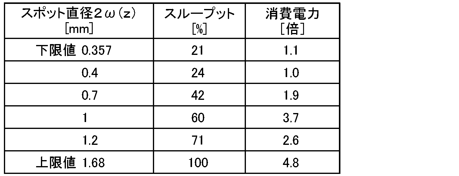
さて、図8に戻り、CPU71は、各スポット直径2ω(z)に応じてスループット及び消費電力を算出した後、スループットと消費電力との対応関係をディスプレイ80に表示する(S240)。その一例を図12に示す。図12には条件1~5のそれぞれにつきスループットと消費電力との対応関係をディスプレイ80に表示した様子を示す。条件1~5はそれぞれスポット直径2ωが0.4[mm]、0.7[mm]、1.0[mm]、1.2[mm]、1.68[mm]のときの対応関係である。ディスプレイ80には、オペレータが条件1~5のいずれかにカーソルを合わせてその条件を選択設定できるように表示される。
続いて、CPU71は、いずれかの対応関係がオペレータによって選択設定されたか否かを判定し(S250)、選択設定されていなければ再びS250に戻る。一方、選択設定されたならば、CPU71は、選択設定された対応関係に基づいてスポット直径2ω(z)を決定し(S260)、レーザ照射条件設定処理を終了する。例えば、条件4が選択設定されたならば、CPU71はスポット直径2ω(z)を1.2[mm]に設定する。
ここで、本実施形態のレーザ照射装置50の主要な要素と本開示のレーザ照射装置の主要な要素との対応関係について説明する。即ち、本実施形態のレーザ照射装置50のレーザヘッド56が本開示のレーザ照射装置の「ヘッド」に相当し、ステージ12が「ステージ」に相当し、Z軸スライダ54及びZ軸アクチュエータ55が「垂直方向移動装置」に相当し、制御装置70が「制御装置」に相当し、ディスプレイ80が「表示装置」に相当する。また、図8の条件5のスループットと消費電力との対応関係が「第1の対応関係」に相当し、条件1のスループットと消費電力との対応関係が「第2の対応関係」に相当し、条件2~4のスループットと消費電力との対応関係が「第3の対応関係」に相当する。
以上説明した本実施形態のレーザ照射装置50は、調整可能な複数のスポット直径2ω(z)の各々に応じて、導体パターンの全体にレーザを照射することにより導体パターンの全体を焼成する際のスループット及び消費電力を導出する。そして、複数のレーザスポット直径2ω(z)の各々に応じて導出されたスループットと消費電力とを対応づけてディスプレイ80に表示する。これにより、オペレータは、ディスプレイ80に表示されたスループットと消費電力との対応関係の中から、バランスがよいものを選出することができる。その結果、スループットと消費電力の両方が適切なバランスとなるようなレーザ照射条件を設定することができる。
また、オペレータはディスプレイ80の画面上でバランスのよいスループットと消費電力との対応関係を選択することができる。特に、スループットと消費電力との対応関係として、スループットが最大の場合の対応関係(条件5)と、消費電力が最小の場合の対応関係(条件1)と、スループットが最大よりも小さく消費電力が最小よりも大きい場合の対応関係(条件2~4)とが表示される。そのため、オペレータはディスプレイ80の画面上に表示されたこれらの対応関係の中からバランスがよいものを選出することができる。
更に、設定可能範囲内(下限値から上限値までの範囲内)のスポット直径2ω(z)であれば、パワー設定の分解能に拘わらず導電パターンの焼成に必要なパワー密度を実現するためのパワー設定が可能となる。そのため、パワー密度範囲内でレーザを照射することにより、導電パターンの焼成を適切に行うことができる。
なお、本発明は上述した実施形態に何ら限定されることはなく、本発明の技術的範囲に属する限り種々の態様で実施し得ることはいうまでもない。
例えば、上述した実施形態では、ディスプレイ80に条件1~5のスループットと消費電力との対応関係をテーブルで表示したが、特にこれに限定されるものではなく、例えばグラフで表示してもよい。
上述した実施形態では、ステージ12をY軸方向に移動させながらレーザを照射する場合を例示したが、特にこれに限定するものではなく、例えばガルバノスキャナやポリゴンミラーなどを用いてレーザを照射するようにしてもよい。
上述した実施形態では、基材の被処理部にレーザ照射する一例として、導電パターンにレーザ照射して焼成する場合を例示したが、特にこれに限定されるものではない。例えば、基材の表面にレーザ照射して表面処理を行うようにしてもよいし、未硬化樹脂にレーザ照射してその樹脂を硬化させてもよい。
上述した実施形態では、レーザヘッド56を搭載したZ軸スライダ54をZ軸方向に移動させることによりスポット直径2ω(z)を調整するようにしたが、これに代えて又は加えて、昇降機構付きの作業用ステージをステージ12の上面に設けてもよい。この場合、作業用ステージ上で樹脂層や配線層を形成するようにし、作業用ステージをレーザヘッド56に対してZ軸方向に移動させることによりスポット直径2ω(z)を調整してもよい。
本開示のレーザ照射装置は、以下のように構成してもよい。
本開示のレーザ照射装置において、前記制御装置は、前記表示装置に表示された前記スループットと前記消費電力との対応関係の中からオペレータが任意の対応関係を選択設定可能な画面を前記表示装置に表示してもよい。こうすれば、オペレータは表示装置の画面上でバランスのよいスループットと消費電力との対応関係を選択設定することができる。
本開示のレーザ照射装置において、前記制御装置は、前記スループットと前記消費電力との対応関係として、少なくとも、前記スループットが最大の場合の前記対応関係である第1の対応関係と、前記消費電力が最小の場合の前記対応関係である第2の対応関係と、前記スループットが最大よりも小さく前記消費電力が最小よりも大きい場合の前記対応関係である第3の対応関係とを前記表示装置に表示してもよい。こうすれば、オペレータは表示装置の画面上に表示された第1~第3の対応関係の中からバランスがよいものを選出することができる。なお、第3の対応関係は、1組だけ表示されてもよいし、複数組表示されてもよい。
本開示のレーザ照射装置において、前記レーザ光源は、所定のパワー分解能でパワー設定を変更可能であり、前記制御装置は、前記被処理部の処理に必要とされるパワー密度範囲を取得し、前記所定のパワー分解能をレーザスポットの面積で除したパワー密度分解能が前記パワー密度範囲の上下限幅に一致するレーザスポット直径をスポット直径下限値として導出し、前記パワー密度範囲の下限値であるパワー密度下限値とレーザスポット面積との積がレーザパワーの上限値になるときのレーザスポット直径をスポット直径上限値として導出し、前記スポット直径下限値から前記スポット直径上限値までの範囲内で、前記垂直方向移動装置によって調整可能な複数のレーザスポット直径を選出してもよい。スポット直径下限値からスポット直径上限値までの範囲内のレーザスポット直径であれば、パワー設定の分解能に拘わらず被処理部の処理に必要なパワー密度を実現するためのパワー設定が可能となる。そのため、パワー密度範囲内でレーザを照射することにより、被処理部の処理を適切に行うことができる。
本開示のレーザ照射装置において、前記スループットは、レーザスポット直径の関数であってレーザスポット直径が大きいほど大きくなるパラメータであり、前記消費電力は、前記被処理部の全体にわたってレーザを照射するのに要する照射時間と前記被処理部にレーザを照射する際のレーザパワーとの積であってもよい。
本発明は、基材の被処理部にレーザを照射する技術に利用可能である。
10 配線基材製造装置、12 ステージ、20 搬送装置、22 Y軸ガイドレール、24 ベルト駆動装置、30 樹脂層形成ユニット、32 インクヘッド、34 UV光照射装置、40 配線層形成ユニット、42 インクヘッド、50 レーザ照射装置、51 台座、52 X軸スライダ、52a X軸ガイドレール、53 X軸アクチュエータ、54 Z軸スライダ、54a Z軸ガイドレール、55 Z軸アクチュエータ、56 レーザヘッド、58 レーザ光源、59 光学系、60 レーザスポット、62 導電パターン、70 制御装置、71 CPU、72 ROM、73 HDD、74 RAM、75 入出力インタフェース、76 バス、80 ディスプレイ。
Claims (5)
- 基材の被処理部にレーザを照射するレーザ照射装置であって、
レーザ光源を有するヘッドと、
前記基材が載置されるステージと、
前記ステージと前記ヘッドとを垂直方向に相対移動させて前記基材の前記被処理部に照射されるレーザスポット直径を調整可能な垂直方向移動装置と、
調整可能な複数のレーザスポット直径の各々に応じて、前記基材の前記被処理部の全体にわたってレーザを照射する際のスループット及び消費電力を求め、前記スループットと前記消費電力とを対応づけて表示装置に表示する制御装置と、
を備えたレーザ照射装置。 - 前記制御装置は、前記表示装置に表示された前記スループットと前記消費電力との対応関係の中からオペレータが任意の対応関係を選択設定可能な画面を前記表示装置に表示する、
請求項1に記載のレーザ照射装置。 - 前記制御装置は、前記スループットと前記消費電力との対応関係として、少なくとも、前記スループットが最大の場合の前記対応関係である第1の対応関係と、前記消費電力が最小の場合の前記対応関係である第2の対応関係と、前記スループットが最大よりも小さく前記消費電力が最小よりも大きい場合の前記対応関係である第3の対応関係とを前記表示装置に表示する、
請求項1又は2に記載のレーザ照射装置。 - 前記レーザ光源は、所定のパワー分解能でパワー設定を変更可能であり、
前記制御装置は、前記被処理部の処理に必要とされるパワー密度範囲を取得し、前記所定のパワー分解能をレーザスポットの面積で除したパワー密度分解能が前記パワー密度範囲の上下限幅に一致するレーザスポット直径をスポット直径下限値として導出し、前記パワー密度範囲の下限値であるパワー密度下限値とレーザスポット面積との積がレーザパワーの上限値になるときのレーザスポット直径をスポット直径上限値として導出し、前記スポット直径下限値から前記スポット直径上限値までの範囲内で、前記垂直方向移動装置によって調整可能な複数のレーザスポット直径を選出する、
請求項1~3のいずれか1項に記載のレーザ照射装置。 - 前記スループットは、レーザスポット直径の関数であってレーザスポット直径が大きいほど大きくなるパラメータであり、
前記消費電力は、前記被処理部の全体にわたってレーザを照射するのに要する照射時間と前記被処理部にレーザを照射する際のレーザパワーとの積である、
請求項1~4のいずれか1項に記載のレーザ照射装置。
Priority Applications (2)
| Application Number | Priority Date | Filing Date | Title |
|---|---|---|---|
| JP2018548490A JP6670946B2 (ja) | 2016-11-01 | 2016-11-01 | レーザ照射装置 |
| PCT/JP2016/082483 WO2018083741A1 (ja) | 2016-11-01 | 2016-11-01 | レーザ照射装置 |
Applications Claiming Priority (1)
| Application Number | Priority Date | Filing Date | Title |
|---|---|---|---|
| PCT/JP2016/082483 WO2018083741A1 (ja) | 2016-11-01 | 2016-11-01 | レーザ照射装置 |
Publications (1)
| Publication Number | Publication Date |
|---|---|
| WO2018083741A1 true WO2018083741A1 (ja) | 2018-05-11 |
Family
ID=62075885
Family Applications (1)
| Application Number | Title | Priority Date | Filing Date |
|---|---|---|---|
| PCT/JP2016/082483 Ceased WO2018083741A1 (ja) | 2016-11-01 | 2016-11-01 | レーザ照射装置 |
Country Status (2)
| Country | Link |
|---|---|
| JP (1) | JP6670946B2 (ja) |
| WO (1) | WO2018083741A1 (ja) |
Citations (5)
| Publication number | Priority date | Publication date | Assignee | Title |
|---|---|---|---|---|
| JP2008062259A (ja) * | 2006-09-06 | 2008-03-21 | Keyence Corp | レーザ加工装置、レーザ加工方法及びレーザ加工プログラム |
| JP2008221765A (ja) * | 2007-03-15 | 2008-09-25 | Oki Data Corp | 印刷装置 |
| JP2012008911A (ja) * | 2010-06-28 | 2012-01-12 | Casio Electronics Co Ltd | 印刷制御装置 |
| JP2013038251A (ja) * | 2011-08-09 | 2013-02-21 | Fanuc Ltd | 電力計算手段を備えたガスレーザ装置 |
| WO2014038241A1 (ja) * | 2012-09-05 | 2014-03-13 | 三菱電機株式会社 | レーザ加工装置 |
-
2016
- 2016-11-01 WO PCT/JP2016/082483 patent/WO2018083741A1/ja not_active Ceased
- 2016-11-01 JP JP2018548490A patent/JP6670946B2/ja not_active Expired - Fee Related
Patent Citations (5)
| Publication number | Priority date | Publication date | Assignee | Title |
|---|---|---|---|---|
| JP2008062259A (ja) * | 2006-09-06 | 2008-03-21 | Keyence Corp | レーザ加工装置、レーザ加工方法及びレーザ加工プログラム |
| JP2008221765A (ja) * | 2007-03-15 | 2008-09-25 | Oki Data Corp | 印刷装置 |
| JP2012008911A (ja) * | 2010-06-28 | 2012-01-12 | Casio Electronics Co Ltd | 印刷制御装置 |
| JP2013038251A (ja) * | 2011-08-09 | 2013-02-21 | Fanuc Ltd | 電力計算手段を備えたガスレーザ装置 |
| WO2014038241A1 (ja) * | 2012-09-05 | 2014-03-13 | 三菱電機株式会社 | レーザ加工装置 |
Also Published As
| Publication number | Publication date |
|---|---|
| JP6670946B2 (ja) | 2020-03-25 |
| JPWO2018083741A1 (ja) | 2019-09-19 |
Similar Documents
| Publication | Publication Date | Title |
|---|---|---|
| JP6615903B2 (ja) | レーザ照射装置 | |
| US11718022B2 (en) | Methods and apparatus for selectively combining particulate material | |
| CN104972121B (zh) | 三维造型装置 | |
| US10882137B2 (en) | Three-dimensional manufacturing method and three-dimensional manufacturing apparatus | |
| US10726635B2 (en) | Three-dimensional shape data editing apparatus, three-dimensional modeling apparatus, three-dimensional modeling system, and non-transitory computer readable medium storing three-dimensional shape data editing program | |
| AU2016273983A1 (en) | 3D printing device for producing a spatially extended product | |
| CN105939837A (zh) | 对用于增材制造系统的切片数据进行处理 | |
| CN108712956B (zh) | 形成三维物体 | |
| CN107521093A (zh) | 用于热塑料选择性激光烧结的行式激光成像器 | |
| JP6441955B2 (ja) | 配線基板作製方法および配線基板作製装置 | |
| JP2015139957A (ja) | 三次元造形装置および三次元造形方法 | |
| US12594716B2 (en) | Shaping method and shaping device | |
| US20240153846A1 (en) | Systems for thermal management and methods thereof | |
| JP2020026577A (ja) | 三次元造形物を製造する方法、三次元造形装置 | |
| JP6586725B2 (ja) | 印刷装置、印刷システム、印刷物の製造方法、およびプログラム | |
| JP5361916B2 (ja) | レーザスクライブ方法 | |
| JP6670946B2 (ja) | レーザ照射装置 | |
| JPWO2017006412A1 (ja) | 造形装置および造形方法 | |
| JPWO2016075822A1 (ja) | 配線基板作製方法および配線基板作製装置 | |
| WO2017221347A1 (ja) | 回路形成方法、および回路形成装置 | |
| JP5584560B2 (ja) | レーザスクライブ方法 | |
| JP2015193217A (ja) | 印刷装置、印刷システム、印刷物の製造方法、およびプログラム | |
| JP2015036234A (ja) | 三次元造形装置および三次元造形方法 | |
| JP2006165402A (ja) | はんだ付け装置とはんだ付け方法 | |
| JP6751135B2 (ja) | 積層体作製装置 |
Legal Events
| Date | Code | Title | Description |
|---|---|---|---|
| 121 | Ep: the epo has been informed by wipo that ep was designated in this application |
Ref document number: 16920647 Country of ref document: EP Kind code of ref document: A1 |
|
| ENP | Entry into the national phase |
Ref document number: 2018548490 Country of ref document: JP Kind code of ref document: A |
|
| NENP | Non-entry into the national phase |
Ref country code: DE |
|
| 122 | Ep: pct application non-entry in european phase |
Ref document number: 16920647 Country of ref document: EP Kind code of ref document: A1 |