WO2018074204A1 - 撮像カメラおよび多眼撮像装置 - Google Patents
撮像カメラおよび多眼撮像装置 Download PDFInfo
- Publication number
- WO2018074204A1 WO2018074204A1 PCT/JP2017/035786 JP2017035786W WO2018074204A1 WO 2018074204 A1 WO2018074204 A1 WO 2018074204A1 JP 2017035786 W JP2017035786 W JP 2017035786W WO 2018074204 A1 WO2018074204 A1 WO 2018074204A1
- Authority
- WO
- WIPO (PCT)
- Prior art keywords
- imaging camera
- holding member
- substrate
- imaging
- recess
- Prior art date
- Legal status (The legal status is an assumption and is not a legal conclusion. Google has not performed a legal analysis and makes no representation as to the accuracy of the status listed.)
- Ceased
Links
Images


Classifications
-
- H—ELECTRICITY
- H04—ELECTRIC COMMUNICATION TECHNIQUE
- H04N—PICTORIAL COMMUNICATION, e.g. TELEVISION
- H04N13/00—Stereoscopic video systems; Multi-view video systems; Details thereof
- H04N13/20—Image signal generators
- H04N13/204—Image signal generators using stereoscopic image cameras
- H04N13/239—Image signal generators using stereoscopic image cameras using two two-dimensional [2D] image sensors having a relative position equal to or related to the interocular distance
-
- G—PHYSICS
- G02—OPTICS
- G02B—OPTICAL ELEMENTS, SYSTEMS OR APPARATUS
- G02B7/00—Mountings, adjusting means, or light-tight connections, for optical elements
- G02B7/02—Mountings, adjusting means, or light-tight connections, for optical elements for lenses
-
- G—PHYSICS
- G03—PHOTOGRAPHY; CINEMATOGRAPHY; ANALOGOUS TECHNIQUES USING WAVES OTHER THAN OPTICAL WAVES; ELECTROGRAPHY; HOLOGRAPHY
- G03B—APPARATUS OR ARRANGEMENTS FOR TAKING PHOTOGRAPHS OR FOR PROJECTING OR VIEWING THEM; APPARATUS OR ARRANGEMENTS EMPLOYING ANALOGOUS TECHNIQUES USING WAVES OTHER THAN OPTICAL WAVES; ACCESSORIES THEREFOR
- G03B19/00—Cameras
- G03B19/02—Still-picture cameras
- G03B19/04—Roll-film cameras
- G03B19/07—Roll-film cameras having more than one objective
-
- G—PHYSICS
- G03—PHOTOGRAPHY; CINEMATOGRAPHY; ANALOGOUS TECHNIQUES USING WAVES OTHER THAN OPTICAL WAVES; ELECTROGRAPHY; HOLOGRAPHY
- G03B—APPARATUS OR ARRANGEMENTS FOR TAKING PHOTOGRAPHS OR FOR PROJECTING OR VIEWING THEM; APPARATUS OR ARRANGEMENTS EMPLOYING ANALOGOUS TECHNIQUES USING WAVES OTHER THAN OPTICAL WAVES; ACCESSORIES THEREFOR
- G03B35/00—Stereoscopic photography
- G03B35/08—Stereoscopic photography by simultaneous recording
-
- H—ELECTRICITY
- H04—ELECTRIC COMMUNICATION TECHNIQUE
- H04N—PICTORIAL COMMUNICATION, e.g. TELEVISION
- H04N23/00—Cameras or camera modules comprising electronic image sensors; Control thereof
- H04N23/50—Constructional details
- H04N23/54—Mounting of pick-up tubes, electronic image sensors, deviation or focusing coils
-
- H—ELECTRICITY
- H04—ELECTRIC COMMUNICATION TECHNIQUE
- H04N—PICTORIAL COMMUNICATION, e.g. TELEVISION
- H04N23/00—Cameras or camera modules comprising electronic image sensors; Control thereof
- H04N23/50—Constructional details
- H04N23/55—Optical parts specially adapted for electronic image sensors; Mounting thereof
-
- H—ELECTRICITY
- H04—ELECTRIC COMMUNICATION TECHNIQUE
- H04N—PICTORIAL COMMUNICATION, e.g. TELEVISION
- H04N2213/00—Details of stereoscopic systems
- H04N2213/001—Constructional or mechanical details
Definitions
- the present invention relates to an imaging camera and a multi-lens imaging apparatus, for example, a coupling structure of a lens component and an imaging element.
- Patent Document 1 Japanese Patent Application Laid-Open No. 2014-179795 discloses a solid-state imaging device having a protrusion on a wiring board.
- the protrusion is formed along the adhesion region at a predetermined distance from the adhesion region between the holder and the wiring board, and an adhesive for bonding the holder to the wiring substrate is applied.
- Patent Document 2 Japanese Patent Laid-Open No. 2008-191552 shows an adhesive connection part between parts in which the edge part of the other part is abutted against one part and bonded with an adhesive. .
- Concave portions are formed on both sides in the thickness direction of the tip of the edge portion, the abutting convex portions between the concave portions are bonded to one part with an adhesive, and the concave portions on both sides are formed of the adhesive. Accommodates extra parts.
- Patent Document 1 and Patent Document 2 described above show the configuration of an imaging camera in which a holder for holding a lens and a wiring board on which an imaging element is mounted are fixed with an adhesive.
- a fixing material such as an adhesive hangs or separates at the time of manufacture, thereby causing contamination of the imaging element, cracks, and a decrease in adhesive strength. There is a fear.
- the present invention has been made in view of such circumstances, and one of its purposes is to provide an imaging camera and a multi-lens imaging device capable of suppressing dripping of a fixing material generated during manufacturing.
- An imaging camera includes a substrate on which an imaging device is mounted, an optical lens that forms a subject image on the imaging device, a holding member that holds the optical lens and surrounds the periphery of the imaging device, and a substrate. And a fixing member for fixing the holding member.
- the holding member is a circumferential surface facing the substrate, and has a coupling surface fixed to the substrate via a fixing material.
- One section in the circumferential direction of the coupling surface includes a corner, and the holding member has a recess at the corner that opens to the image sensor side.
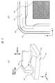
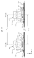
- FIG. 2A is a plan view showing an example of an outer shape in a state where the imaging camera of FIG. 1A is assembled
- FIG. 2B is a cross-sectional view showing a structural example between AA ′ in FIG.
- FIG. (A) is a perspective view which shows an example of the shape of a recessed part and a fixing material in the imaging camera of FIG. 1 (a) and FIG.1 (b), (b) expanded a part of (a). It is a top view.
- FIG.3 (a) and FIG.3 (b) is a figure used as the 1st comparative example of Drawing 3 (a) and Drawing 3 (b), respectively.
- (A), (b) and (c) is sectional drawing explaining the mechanism by which the shape of Fig.3 (a) and FIG.3 (b) is obtained.
- (A) is a perspective view which shows the detailed structural example of the holding member of Fig.3 (a)
- (b) is a perspective view which shows the 2nd comparative example of (a).
- A) is the perspective view which shows the structural example around a holding member in the imaging camera by Embodiment 2 of this invention
- (b) is the top view which expanded a part of (a).
- (A) is a perspective view which shows the structural example around a holding member in the imaging camera by Embodiment 3 of this invention
- (b) is the top view which expanded a part of (a).
- Each of (a) and (b) is a cross-sectional view showing an example of the structure around the holding member in the imaging camera according to Embodiment 4 of the present invention.
- It is a perspective view which shows the schematic structural example of the multiview imaging device by Embodiment 5 of this invention.
- It is sectional drawing which shows the typical structural example of the multiview imaging device of FIG. It is sectional drawing used as the comparative example of FIG.
- the constituent elements are not necessarily indispensable unless otherwise specified and apparently essential in principle. Needless to say.
- the shapes, positional relationships, etc. of the components, etc. when referring to the shapes, positional relationships, etc. of the components, etc., the shapes are substantially the same unless otherwise specified, or otherwise apparent in principle. And the like are included. The same applies to the above numerical values and ranges.
- FIG. 1A is a perspective view illustrating a schematic configuration example of the imaging camera according to Embodiment 1 of the present invention
- FIG. 1B illustrates a structural example of the holding member in FIG. It is a top view
- FIG. 2A is a plan view showing an example of an outer shape in a state where the imaging camera of FIG. 1A is assembled
- FIG. 2B is a structure between AA ′ in FIG. It is sectional drawing which shows an example.
- the 1A includes an optical lens 110, a holding member 120, a substrate 130, an imaging element 140, and a fixing material 150.
- the imaging camera 100 illustrated in FIG. The optical lens 110 is held and fixed by the holding member 120 and integrated with the holding member 120.
- the image sensor 140 is mounted on the substrate 130, and a fixing material 150 that fixes the substrate 130 and the holding member 120 is applied around the image sensor 140 on the substrate 130.
- the image sensor 140 is typically a CMOS image sensor, a CCD image sensor, or the like.
- the holding member 120 is a circumferential surface facing the substrate 130, and has a bottom surface portion (bonding surface) 121 that is fixed to the substrate 130 via a fixing material 150.
- a corner 122 is included in one section of the bottom surface 121 in the circumferential direction.
- the holding member 120 has a concave portion 124 that opens to the imaging element 140 side at the corner portion 122.
- the bottom surface portion 121 includes four corner portions 122, and the recessed portion 124 is provided in each of the four corner portions 122.
- the bottom surface portion (bonding surface) 121 of the holding member 120 is in contact with the fixing material 150, and the holding member 120 is an image sensor.
- the substrate 140 is fixed to the substrate 130 via the fixing member 150 in a state of surrounding the 140.
- the holding member 120 and the substrate 130 are such that the optical axis 160 of the optical lens 110 integrated with the holding member 120 is substantially perpendicular to the imaging surface of the imaging device 140, and the focal point of the optical lens 110 is on the imaging device 140. It is fixed in a state of almost matching.
- the fixing material 150 is applied to the substrate 130 in a molten state at the time of manufacture, and is solidified in a state where the fixing positions of the holding member 120 and the substrate 130 are fixed, thereby fixing the holding member 120 and the substrate 130.
- any material that solidifies from a melted state such as an adhesive, a resin, and solder, can be considered.
- the optical lens 110 forms visual information (subject image) obtained from the outside world on the image sensor 130, whereby the imaging camera 100 obtains an image of the outside world.
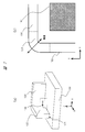
- FIG. 3A is a perspective view showing an example of the shape of the recess and the fixing material in the imaging camera of FIGS. 1A and 1B
- FIG. 3B is a perspective view of FIG. It is the top view to which a part of was expanded.
- 4 (a) and 4 (b) are diagrams respectively showing a first comparative example of FIGS. 3 (a) and 3 (b).
- 5 (a), 5 (b), and 5 (c) are cross-sectional views illustrating the mechanism by which the shapes of FIGS. 3 (a) and 3 (b) are obtained.
- the positional relationship between 110 and the image sensor 140 is ideal.
- the manufacturing process of the imaging camera 100 includes a step of adjusting the positional relationship between the optical lens 110 and the imaging element 140 and a step of solidifying the fixing material 150 that has been in a molten state at the adjustment position. Including. As a result, desired optical performance can be obtained.
- the fixing material 150 in the melt state has a surface tension. May accumulate at the corners of the holding member 120 ′. Such a phenomenon is due to a capillary phenomenon, and the inner wall located at the corner of the holding member 120 ′ functions like a thin tube.
- the fixing material 150 accumulated in the corners hangs down, so that the fixing material 150 adheres to the imaging element 140, and the attached fixing material 150 becomes the imaging element. 140 may cause contamination or cracking due to thermal stress. Furthermore, since the fixing material 150 accumulates at the corners, the application amount of the fixing material 150 may decrease at the side portions other than the corners of the holding member 120 ′. As a result, the fixing member 150 may be thinned or separated at the side portion of the holding member 120 ′, which may cause a reduction in fixing strength.
- the holding member 120 has a concave portion 124 that opens to the imaging element 140 side at the corner.
- the corner fixing member 150 has a shape stored inside the recess 124, and accordingly, the corner member is prevented from being accumulated in the corner more than the volume of the recess 124.
- the mechanism by which the corner fixing member 150 is stored inside the recess 124 can be explained by the wetting and spreading behavior of the fixing member 150 in the holding member 120.
- the concave portion 124 sucks the fixing material 150 by capillary action, and is shown in FIG. 5B.
- Such a wet shape of the fixing material 150 is temporarily formed.
- the fixing material 150 in a situation where the fixing material 150 is attached to the upper wall W1 of the recess 124, the fixing material 150 has its own surface tension, the surface tension of the holding member 120, and the fixing material 150. And the interfacial tension between the holding member 120 and the wet contact spread determined in a state where the wet contact angle is generally maintained. However, in order for the fixing member 150 to spread out over the edge EG1 of the upper wall W1, as shown in FIG. 5 (c), the fixing member 150 having a larger contact angle than the situation of FIG. 5 (b). It is necessary to spread wet through the shape.
- the fixing member 150 In order to wet and spread through such a shape of the fixing material 150, it is necessary to supply a large amount of the fixing material 150 and a driving force of strong wetting and spreading compared with the situation of FIG. For this reason, the fixing member 150 whose corners are wetted by capillary action cannot get over the edge EG1 of the recess 124 formed in the corners. As a result, the fixing material 150 is sucked into the recess 124 and further stored inside the recess 124.
- the size h2 in the height direction of the recess 124 is larger than the size h1 in the height direction of the fixing material 150 when applied to the substrate 130. If the size h2 of the recess 124 is smaller than the size h1 of the fixing material 150, the fixing material 150 exceeds the edge EG1 at the moment when the holding member 120 is pressed against the fixing material 150 as shown in FIG. This is because there is a risk of losing. ⁇ Main effects of the first embodiment >>
- FIG. 6A is a perspective view showing a detailed structural example of the holding member in FIG. 3A
- FIG. 6B is a perspective view showing a second comparative example in FIG. 6A. is there.
- the recess 124 forms a space that is closed by the wall except for the image sensor 140 side in a state where the holding member 120 is fixed to the substrate 130.
- the recess 124 includes a top wall W1, side walls W2a and W2b, and a back wall W3.
- the upper wall W1 is a wall with respect to the direction perpendicular to the surface of the substrate 130 (Z-axis direction).
- the side walls W ⁇ b> 2 a and W ⁇ b> 2 b are walls with respect to the circumferential direction R of the bottom surface portion (coupling surface) 121.
- the back wall W ⁇ b> 3 is a wall in the direction from the inner peripheral side to the outer peripheral side of the bottom surface part 121.
- the wetting of the fixing material is suppressed so as not to exceed the edge EG1 of the upper wall W1 as described in FIG. 5C. Furthermore, wetting of the fixing material is suppressed so as not to exceed the edge EG2 of the side walls W2a and W2b for the same reason.
- the fixing material is stored inside the recess 124 by the two deterrence forces.
- the fixing material 150 can be prevented from being thinned or separated. If the fixing member 150 can be prevented from being thinned or separated, the positional relationship between the holding member 120 (and thus the optical lens 110) and the substrate 130 can be kept constant, and the bonding strength between the holding member 120 and the substrate 130 can be kept constant. Can also keep well.
- FIG. 6B unlike the structure of FIG. 6A, a holding member 120 ′′ having a concave portion on the entire inner periphery of the bottom surface portion is shown in addition to the corner portion. 4A and 4B, wetting and spreading are performed starting from the corners in the same manner as in the case of Fig. 4. In this case, unlike the case of Fig. 4A, the wetting and spreading of the fixing material is caused by the wall W1 on the upper surface. It is suppressed by “edge EG1”.
- each of the side walls W2a and W2b exerts a force directed in the direction perpendicular to the wall as shown in FIG. 6A. It can be received as a force in the pulling direction.
- the bonding strength particularly shear strength
- the holding member 120 and the substrate 130. May be increased.
- FIG. 7A is a perspective view showing a structural example around the holding member in the imaging camera according to Embodiment 2 of the present invention
- FIG. 7B is an enlarged view of a part of FIG. It is a top view.
- the imaging camera according to the second embodiment is different from the imaging camera according to the first embodiment in the shape of the recess 124 included in the holding member 120.
- the concave portion 124 provided in the corner portion 122 is formed with the inner periphery of the circular bottom surface portion (coupling surface) 121 in a state where the holding member 120 is fixed to the substrate 130.
- a tunnel-like space penetrating the outer periphery is formed.
- the fixing member 150 images the corner portion 124 as compared with the first embodiment. Since it becomes difficult to accumulate on the element 140 side, the drooping of the fixing material 150 toward the imaging element 140 may be further suppressed. However, depending on the material of the fixing member 150 and the like, external light may leak to the image sensor 140 side through the concave portion 124. From this viewpoint, the structure of the first embodiment is desirable. (Embodiment 3) ⁇ Details around the holding member and the fixing material (modified example) >>
- FIG. 8A is a perspective view showing an example of the structure around the holding member in the imaging camera according to Embodiment 3 of the present invention
- FIG. 8B is an enlarged view of a part of FIG. 8A. It is a top view.
- the imaging camera of the third embodiment is compared with the imaging camera of the first embodiment at one corner 122 of the holding member 120. The difference is that a plurality of (here, three) recesses 124a, 124b, and 124c are provided.
- one recess 124 provided at a corner as shown in FIGS. 3A and 3B functions as a single capillary that sucks the fixing material 150, , It plays a role of confining inside the recess 124.
- the volume of the concave portion 124 is determined in consideration of how much of the total amount of the fixing material 150 is distributed to the side portion.
- the volume required by the recess 124 is increased, for example, it may be necessary to widen the interval between the side walls W2a and W2b shown in FIG.
- each of the recesses 124a, 124b, and 124c functions as a thin capillary tube, and can strongly suck the fixing material 150, and in addition, the sucked fixing material 150 can be confined inside itself with a strong force.
- the plurality of recesses are more due to capillary action than in the first embodiment. Since the fixing material 150 is positively sucked and stored inside the recess, it is possible to further suppress the drooping of the fixing material 150 toward the image sensor 140 side. Further, even when the overall volume of the recess is increased to some extent, it is possible to cope with it, so that the degree of freedom in determining the volume of the recess can be increased. (Embodiment 4) ⁇ Details around the holding member and the fixing material (modified example) >>
- FIG. 9A and FIG. 9B are cross-sectional views showing an example of the structure around the holding member in the imaging camera according to Embodiment 4 of the present invention.
- the imaging camera according to the fourth embodiment differs from the imaging camera according to the first embodiment in the shape of the recess 124 included in the holding member 120.
- the recess 124 is further provided with a second recess 125.
- the concave portion 124 and the second concave portion 125 form a stepped step when viewed in a plane (XZ plane) perpendicular to the plane of the substrate 130.
- the fixing member 150 can be more reliably recessed than the case of the first embodiment. Can be stored inside. Specifically, as described in FIG. 5A and the like, for example, when the size h1 of the fixing material 150 in the height direction is larger than the size h2 of the concave portion 124 in the height direction due to some factor, the fixing is performed. The material 150 may exceed the edge EG1. On the other hand, in FIG. 9A (the same applies to FIG. 9B), by providing the second recess 125, the top walls W11 and W12 and the edges EG11 and EG12 are arranged stepwise. Even if the fixing material 150 exceeds the edge EG11, the edge EG12 can suppress the wetting of the fixing material. (Embodiment 5) ⁇ Configuration of multi-eye imaging device>
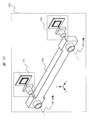
- FIG. 10 is a perspective view showing a schematic configuration example of the multi-lens imaging apparatus according to the fifth embodiment of the present invention.
- a multi-lens imaging device 400 illustrated in FIG. 10 includes an imaging camera 100, a second imaging camera 200, and a housing 300.
- the second imaging camera 200 has a structure equivalent to that of the imaging camera 100.
- the housing 300 fixes the imaging camera 100 and the second imaging camera 200 at positions separated by a predetermined distance so that the optical axes 160 of each other are substantially parallel.
- the multi-eye imaging device 400 detects a coincidence point between images acquired by the imaging camera 100 and the second imaging camera 200, and synthesizes both images to generate a distance image including three-dimensional information of the outside world. For this reason, when the distance information of the outside world is acquired by the multi-lens imaging device 400, it is desirable that the optical characteristics of the imaging cameras included in the multi-lens imaging device 400 match.
- defocus temperature characteristic As an example of the optical characteristics of the imaging camera related to the acquisition of distance information, there is a focus position response characteristic with respect to temperature (hereinafter, defocus temperature characteristic). For example, when the defocus temperature characteristics are greatly different in each imaging camera included in the multi-lens imaging device 400, the resolution of the image acquired by each imaging camera varies when the external temperature changes. In such a state, it becomes difficult to detect the coincidence point of the images obtained by the respective imaging cameras, so that the calculation accuracy of the distance in the generated distance image is lowered.
- Such optical characteristics such as defocus temperature characteristics depend on the structure and configuration of an optical lens, a holding member, a fixing material, an imaging element, and a substrate included in the imaging camera.
- the fixing material applied in the melt state at the time of manufacture causes a variation in shape by accumulating at the corners of the holding member, as described above, and thus can be a main factor of variations in optical characteristics. Therefore, it is beneficial to apply the configurations described in Embodiments 1 to 4 to the imaging camera 100 and the second imaging camera 200, respectively.
- FIG. 11 is a cross-sectional view showing a schematic structural example of the multi-lens imaging device of FIG. 10, and FIG. 12 is a cross-sectional view as a comparative example of FIG.
- both the imaging camera 100 ′ and the second imaging camera 200 ′ are provided with the holding member 120 ′ shown in FIGS. 4 (a) and 4 (b).
- the optical axis 160 is not parallel between the imaging camera 100 ′ and the second imaging camera 200 ′, and the positional relationship between the optical lens 110 and the imaging element 140 is also different from each other. Can happen.
- misalignment occurs when the holding member 120 ′ is pressed against the fixing material 150, and the amount of the fixing material 150 accumulated differs at the two corners.
- the amount of the fixing material 150 in the side portion of the holding member 120 ′ may be different for each side portion, and the optical axis 160 may be inclined.
- the adhesive force at the two corners may change with the outside temperature.
- the optical axis 160 is not tilted at the time of manufacture, there is a possibility that the tilt may occur with a change in the outside temperature.
- the accumulation amount of the fixing material 150 at each corner can be kept substantially constant according to the volume of the recess 124 as described in each embodiment. .
- the amount of the fixing material 150 at the side portion of the holding member 120 can be kept substantially constant at each side portion, and the adhesive force at each corner portion can also be kept substantially constant regardless of the external temperature.
- the optical axes 160 of the imaging camera 100 and the second imaging camera 200 can be kept substantially parallel, and the coincidence points of the images obtained by the respective imaging cameras can be easily obtained. It becomes possible to detect.
- the multi-lens imaging device of the fifth embodiment in addition to obtaining the same effect as in the first to fourth embodiments, it is possible to suppress variation in the shape of the fixing material in each imaging camera. It is possible to prevent the distance calculation accuracy of the multi-lens imaging device from deteriorating due to factors such as temperature changes.
- the present invention made by the present inventor has been specifically described based on the embodiment.
- the present invention is not limited to the embodiment, and various modifications can be made without departing from the scope of the invention.
- the above-described embodiment has been described in detail for easy understanding of the present invention, and is not necessarily limited to one having all the configurations described.
- a part of the configuration of one embodiment can be replaced with the configuration of another embodiment, and the configuration of another embodiment can be added to the configuration of one embodiment. .
- the planar shape formed by the inner periphery of the bottom surface portion (coupling surface) of the holding member is a quadrangle having four corner portions is taken as an example.
- the planar shape is not limited to a quadrangle, and may be a shape having one or more corners.
- the corner portion is a portion where two lines intersect at an angle ⁇ (0 ⁇ ⁇ 180 °).
- Imaging camera 110 Optical lens 120 Holding member 121 Bottom surface part (bonding surface) 122 corner 123 side 124, 124a, 124b, 124c recess 125 second recess 130 substrate 140 imaging element 150 fixing material 160 optical axis 200 second imaging camera 300 housing 400 multi-lens imaging device EG1, EG2, EG11, EG12 Edge W1, W2a, W2b, W3, W11, W12 Wall
Landscapes
- Physics & Mathematics (AREA)
- Engineering & Computer Science (AREA)
- Multimedia (AREA)
- Signal Processing (AREA)
- General Physics & Mathematics (AREA)
- Optics & Photonics (AREA)
- Lens Barrels (AREA)
- Studio Devices (AREA)
- Cameras In General (AREA)
- Stereoscopic And Panoramic Photography (AREA)
- Transforming Light Signals Into Electric Signals (AREA)
Priority Applications (1)
| Application Number | Priority Date | Filing Date | Title |
|---|---|---|---|
| EP17861330.3A EP3531697B1 (en) | 2016-10-21 | 2017-10-02 | Imaging camera and multi-eye imaging device |
Applications Claiming Priority (2)
| Application Number | Priority Date | Filing Date | Title |
|---|---|---|---|
| JP2016-206790 | 2016-10-21 | ||
| JP2016206790A JP6535646B2 (ja) | 2016-10-21 | 2016-10-21 | 撮像カメラおよび多眼撮像装置 |
Publications (1)
| Publication Number | Publication Date |
|---|---|
| WO2018074204A1 true WO2018074204A1 (ja) | 2018-04-26 |
Family
ID=62018452
Family Applications (1)
| Application Number | Title | Priority Date | Filing Date |
|---|---|---|---|
| PCT/JP2017/035786 Ceased WO2018074204A1 (ja) | 2016-10-21 | 2017-10-02 | 撮像カメラおよび多眼撮像装置 |
Country Status (3)
| Country | Link |
|---|---|
| EP (1) | EP3531697B1 (enExample) |
| JP (1) | JP6535646B2 (enExample) |
| WO (1) | WO2018074204A1 (enExample) |
Cited By (1)
| Publication number | Priority date | Publication date | Assignee | Title |
|---|---|---|---|---|
| CN112236993A (zh) * | 2018-05-30 | 2021-01-15 | 日本电产科宝株式会社 | 摄像装置 |
Citations (4)
| Publication number | Priority date | Publication date | Assignee | Title |
|---|---|---|---|---|
| JP2006086672A (ja) * | 2004-09-15 | 2006-03-30 | Nidec Copal Corp | 撮像モジュール |
| JP2009224857A (ja) * | 2008-03-13 | 2009-10-01 | Hitachi Maxell Ltd | カメラモジュール及び撮像装置 |
| JP2012155102A (ja) * | 2011-01-25 | 2012-08-16 | Sharp Corp | ステレオカメラユニットおよびその製造方法、電子情報機器 |
| US20160337561A1 (en) * | 2015-05-11 | 2016-11-17 | Samsung Electro-Mechanics Co., Ltd. | Electronic module and method of manufacturing the same |
Family Cites Families (4)
| Publication number | Priority date | Publication date | Assignee | Title |
|---|---|---|---|---|
| JP2007110594A (ja) * | 2005-10-17 | 2007-04-26 | Hitachi Maxell Ltd | カメラモジュール |
| JP2008153720A (ja) * | 2006-12-14 | 2008-07-03 | Hitachi Maxell Ltd | カメラモジュール及び撮像装置 |
| JP5296130B2 (ja) * | 2011-03-22 | 2013-09-25 | シャープ株式会社 | 光学モジュール及び光学モジュールの製造方法 |
| DE102012106834A1 (de) * | 2012-07-27 | 2014-01-30 | Conti Temic Microelectronic Gmbh | Verfahren zur Ausrichtung zweier Bildaufnahmeelemente eines Stereokamerasystems |
-
2016
- 2016-10-21 JP JP2016206790A patent/JP6535646B2/ja active Active
-
2017
- 2017-10-02 WO PCT/JP2017/035786 patent/WO2018074204A1/ja not_active Ceased
- 2017-10-02 EP EP17861330.3A patent/EP3531697B1/en active Active
Patent Citations (4)
| Publication number | Priority date | Publication date | Assignee | Title |
|---|---|---|---|---|
| JP2006086672A (ja) * | 2004-09-15 | 2006-03-30 | Nidec Copal Corp | 撮像モジュール |
| JP2009224857A (ja) * | 2008-03-13 | 2009-10-01 | Hitachi Maxell Ltd | カメラモジュール及び撮像装置 |
| JP2012155102A (ja) * | 2011-01-25 | 2012-08-16 | Sharp Corp | ステレオカメラユニットおよびその製造方法、電子情報機器 |
| US20160337561A1 (en) * | 2015-05-11 | 2016-11-17 | Samsung Electro-Mechanics Co., Ltd. | Electronic module and method of manufacturing the same |
Cited By (1)
| Publication number | Priority date | Publication date | Assignee | Title |
|---|---|---|---|---|
| CN112236993A (zh) * | 2018-05-30 | 2021-01-15 | 日本电产科宝株式会社 | 摄像装置 |
Also Published As
| Publication number | Publication date |
|---|---|
| JP6535646B2 (ja) | 2019-06-26 |
| EP3531697B1 (en) | 2025-06-18 |
| JP2018067869A (ja) | 2018-04-26 |
| EP3531697A1 (en) | 2019-08-28 |
| EP3531697A4 (en) | 2020-08-26 |
Similar Documents
| Publication | Publication Date | Title |
|---|---|---|
| US8045044B2 (en) | Camera module comprising three members | |
| US8810722B2 (en) | Camera module lens holder | |
| US7154156B2 (en) | Solid-state imaging device and method for producing the same | |
| US20140023430A1 (en) | Attachment Techniques | |
| TW201347524A (zh) | 微型相機模組 | |
| JP7449920B2 (ja) | 半導体装置 | |
| CN203705714U (zh) | 影像提取模块 | |
| US9748293B1 (en) | Image sensor packages with folded cover-glass sealing interface | |
| TW201806045A (zh) | 攝像元件、製造方法、及電子機器 | |
| US20180247962A1 (en) | Image sensor package structure and packaging method thereof | |
| TW200405115A (en) | Camera module, holder for use in a camera module, camera system and method of manufacturing a camera module | |
| US9111827B2 (en) | Manufacturing method of solid-state imaging apparatus, solid-state imaging apparatus, and electronic imaging apparatus | |
| JP2015146380A (ja) | 撮像ユニット及び撮像装置 | |
| US20140036146A1 (en) | Camera module and electronic device including the same | |
| WO2018074204A1 (ja) | 撮像カメラおよび多眼撮像装置 | |
| WO2016084394A1 (ja) | 撮像装置 | |
| US20140267893A1 (en) | Image pickup unit and method for manufacturing the same | |
| JP2011022444A (ja) | 接合光学素子 | |
| WO2014192933A1 (ja) | 積層型レンズアレイユニット及び撮像装置 | |
| KR20130096902A (ko) | 자동초점 카메라 모듈 및 그 제조방법 | |
| JP3606756B2 (ja) | 固体撮像装置 | |
| JP7554285B2 (ja) | パッケージおよびセラミックス基板 | |
| JP5919072B2 (ja) | レンズ駆動装置の製造方法 | |
| JP2007194271A (ja) | 撮像素子の実装構造 | |
| JPH0546046U (ja) | 固体撮像装置 |
Legal Events
| Date | Code | Title | Description |
|---|---|---|---|
| 121 | Ep: the epo has been informed by wipo that ep was designated in this application |
Ref document number: 17861330 Country of ref document: EP Kind code of ref document: A1 |
|
| NENP | Non-entry into the national phase |
Ref country code: DE |
|
| ENP | Entry into the national phase |
Ref document number: 2017861330 Country of ref document: EP Effective date: 20190521 |
|
| WWG | Wipo information: grant in national office |
Ref document number: 2017861330 Country of ref document: EP |