WO2018070641A2 - 유기 광전자 소자용 화합물, 유기 광전자 소자 및 표시 장치 - Google Patents
유기 광전자 소자용 화합물, 유기 광전자 소자 및 표시 장치 Download PDFInfo
- Publication number
- WO2018070641A2 WO2018070641A2 PCT/KR2017/006974 KR2017006974W WO2018070641A2 WO 2018070641 A2 WO2018070641 A2 WO 2018070641A2 KR 2017006974 W KR2017006974 W KR 2017006974W WO 2018070641 A2 WO2018070641 A2 WO 2018070641A2
- Authority
- WO
- WIPO (PCT)
- Prior art keywords
- group
- substituted
- formula
- unsubstituted
- compound
- Prior art date
- Legal status (The legal status is an assumption and is not a legal conclusion. Google has not performed a legal analysis and makes no representation as to the accuracy of the status listed.)
- Ceased
Links
- 0 Cc1ccc(C)c(*)c1 Chemical compound Cc1ccc(C)c(*)c1 0.000 description 7
- RVKLVLVNPAZGQA-UHFFFAOYSA-N CCC(CNCC)[I+]C Chemical compound CCC(CNCC)[I+]C RVKLVLVNPAZGQA-UHFFFAOYSA-N 0.000 description 1
- WPCZTFJHMFEXMW-UHFFFAOYSA-N C[BrH]c1ccccc1-c(cccc1)c1-c1c2[s]c(cccc3)c3c2ccc1 Chemical compound C[BrH]c1ccccc1-c(cccc1)c1-c1c2[s]c(cccc3)c3c2ccc1 WPCZTFJHMFEXMW-UHFFFAOYSA-N 0.000 description 1
- IMKBHYVHLCEULU-UHFFFAOYSA-N Cc1c(c2ccccc2[o]2)c2c(c(cccc2)c2c2ccccc22)c2c1 Chemical compound Cc1c(c2ccccc2[o]2)c2c(c(cccc2)c2c2ccccc22)c2c1 IMKBHYVHLCEULU-UHFFFAOYSA-N 0.000 description 1
- DXLQNXJOQRRAHE-UHFFFAOYSA-N Cc1cc2c(ccc3c4[o]c5c3cccc5)c4c(cccc3)c3c2cc1 Chemical compound Cc1cc2c(ccc3c4[o]c5c3cccc5)c4c(cccc3)c3c2cc1 DXLQNXJOQRRAHE-UHFFFAOYSA-N 0.000 description 1
- VVQSFNYDRZXLCN-UHFFFAOYSA-N c(cc1)cc2c1[s]c1c2ccc2c(cccc3)c3c(cccc3)c3c12 Chemical compound c(cc1)cc2c1[s]c1c2ccc2c(cccc3)c3c(cccc3)c3c12 VVQSFNYDRZXLCN-UHFFFAOYSA-N 0.000 description 1
Classifications
-
- C—CHEMISTRY; METALLURGY
- C09—DYES; PAINTS; POLISHES; NATURAL RESINS; ADHESIVES; COMPOSITIONS NOT OTHERWISE PROVIDED FOR; APPLICATIONS OF MATERIALS NOT OTHERWISE PROVIDED FOR
- C09K—MATERIALS FOR MISCELLANEOUS APPLICATIONS, NOT PROVIDED FOR ELSEWHERE
- C09K11/00—Luminescent materials, e.g. electroluminescent or chemiluminescent
- C09K11/06—Luminescent materials, e.g. electroluminescent or chemiluminescent containing organic luminescent materials
-
- C—CHEMISTRY; METALLURGY
- C07—ORGANIC CHEMISTRY
- C07D—HETEROCYCLIC COMPOUNDS
- C07D405/00—Heterocyclic compounds containing both one or more hetero rings having oxygen atoms as the only ring hetero atoms, and one or more rings having nitrogen as the only ring hetero atom
- C07D405/02—Heterocyclic compounds containing both one or more hetero rings having oxygen atoms as the only ring hetero atoms, and one or more rings having nitrogen as the only ring hetero atom containing two hetero rings
- C07D405/04—Heterocyclic compounds containing both one or more hetero rings having oxygen atoms as the only ring hetero atoms, and one or more rings having nitrogen as the only ring hetero atom containing two hetero rings directly linked by a ring-member-to-ring-member bond
-
- C—CHEMISTRY; METALLURGY
- C07—ORGANIC CHEMISTRY
- C07D—HETEROCYCLIC COMPOUNDS
- C07D307/00—Heterocyclic compounds containing five-membered rings having one oxygen atom as the only ring hetero atom
- C07D307/77—Heterocyclic compounds containing five-membered rings having one oxygen atom as the only ring hetero atom ortho- or peri-condensed with carbocyclic rings or ring systems
-
- C—CHEMISTRY; METALLURGY
- C07—ORGANIC CHEMISTRY
- C07D—HETEROCYCLIC COMPOUNDS
- C07D333/00—Heterocyclic compounds containing five-membered rings having one sulfur atom as the only ring hetero atom
- C07D333/50—Heterocyclic compounds containing five-membered rings having one sulfur atom as the only ring hetero atom condensed with carbocyclic rings or ring systems
-
- C—CHEMISTRY; METALLURGY
- C07—ORGANIC CHEMISTRY
- C07D—HETEROCYCLIC COMPOUNDS
- C07D405/00—Heterocyclic compounds containing both one or more hetero rings having oxygen atoms as the only ring hetero atoms, and one or more rings having nitrogen as the only ring hetero atom
- C07D405/02—Heterocyclic compounds containing both one or more hetero rings having oxygen atoms as the only ring hetero atoms, and one or more rings having nitrogen as the only ring hetero atom containing two hetero rings
- C07D405/10—Heterocyclic compounds containing both one or more hetero rings having oxygen atoms as the only ring hetero atoms, and one or more rings having nitrogen as the only ring hetero atom containing two hetero rings linked by a carbon chain containing aromatic rings
-
- C—CHEMISTRY; METALLURGY
- C07—ORGANIC CHEMISTRY
- C07D—HETEROCYCLIC COMPOUNDS
- C07D405/00—Heterocyclic compounds containing both one or more hetero rings having oxygen atoms as the only ring hetero atoms, and one or more rings having nitrogen as the only ring hetero atom
- C07D405/14—Heterocyclic compounds containing both one or more hetero rings having oxygen atoms as the only ring hetero atoms, and one or more rings having nitrogen as the only ring hetero atom containing three or more hetero rings
-
- C—CHEMISTRY; METALLURGY
- C07—ORGANIC CHEMISTRY
- C07D—HETEROCYCLIC COMPOUNDS
- C07D409/00—Heterocyclic compounds containing two or more hetero rings, at least one ring having sulfur atoms as the only ring hetero atoms
- C07D409/02—Heterocyclic compounds containing two or more hetero rings, at least one ring having sulfur atoms as the only ring hetero atoms containing two hetero rings
- C07D409/04—Heterocyclic compounds containing two or more hetero rings, at least one ring having sulfur atoms as the only ring hetero atoms containing two hetero rings directly linked by a ring-member-to-ring-member bond
-
- C—CHEMISTRY; METALLURGY
- C07—ORGANIC CHEMISTRY
- C07D—HETEROCYCLIC COMPOUNDS
- C07D409/00—Heterocyclic compounds containing two or more hetero rings, at least one ring having sulfur atoms as the only ring hetero atoms
- C07D409/02—Heterocyclic compounds containing two or more hetero rings, at least one ring having sulfur atoms as the only ring hetero atoms containing two hetero rings
- C07D409/10—Heterocyclic compounds containing two or more hetero rings, at least one ring having sulfur atoms as the only ring hetero atoms containing two hetero rings linked by a carbon chain containing aromatic rings
-
- C—CHEMISTRY; METALLURGY
- C07—ORGANIC CHEMISTRY
- C07D—HETEROCYCLIC COMPOUNDS
- C07D409/00—Heterocyclic compounds containing two or more hetero rings, at least one ring having sulfur atoms as the only ring hetero atoms
- C07D409/14—Heterocyclic compounds containing two or more hetero rings, at least one ring having sulfur atoms as the only ring hetero atoms containing three or more hetero rings
-
- C—CHEMISTRY; METALLURGY
- C09—DYES; PAINTS; POLISHES; NATURAL RESINS; ADHESIVES; COMPOSITIONS NOT OTHERWISE PROVIDED FOR; APPLICATIONS OF MATERIALS NOT OTHERWISE PROVIDED FOR
- C09K—MATERIALS FOR MISCELLANEOUS APPLICATIONS, NOT PROVIDED FOR ELSEWHERE
- C09K11/00—Luminescent materials, e.g. electroluminescent or chemiluminescent
- C09K11/02—Use of particular materials as binders, particle coatings or suspension media therefor
- C09K11/025—Use of particular materials as binders, particle coatings or suspension media therefor non-luminescent particle coatings or suspension media
-
- H—ELECTRICITY
- H10—SEMICONDUCTOR DEVICES; ELECTRIC SOLID-STATE DEVICES NOT OTHERWISE PROVIDED FOR
- H10K—ORGANIC ELECTRIC SOLID-STATE DEVICES
- H10K50/00—Organic light-emitting devices
- H10K50/10—OLEDs or polymer light-emitting diodes [PLED]
- H10K50/11—OLEDs or polymer light-emitting diodes [PLED] characterised by the electroluminescent [EL] layers
-
- H—ELECTRICITY
- H10—SEMICONDUCTOR DEVICES; ELECTRIC SOLID-STATE DEVICES NOT OTHERWISE PROVIDED FOR
- H10K—ORGANIC ELECTRIC SOLID-STATE DEVICES
- H10K85/00—Organic materials used in the body or electrodes of devices covered by this subclass
- H10K85/60—Organic compounds having low molecular weight
- H10K85/649—Aromatic compounds comprising a hetero atom
- H10K85/654—Aromatic compounds comprising a hetero atom comprising only nitrogen as heteroatom
-
- H—ELECTRICITY
- H10—SEMICONDUCTOR DEVICES; ELECTRIC SOLID-STATE DEVICES NOT OTHERWISE PROVIDED FOR
- H10K—ORGANIC ELECTRIC SOLID-STATE DEVICES
- H10K85/00—Organic materials used in the body or electrodes of devices covered by this subclass
- H10K85/60—Organic compounds having low molecular weight
- H10K85/649—Aromatic compounds comprising a hetero atom
- H10K85/657—Polycyclic condensed heteroaromatic hydrocarbons
- H10K85/6574—Polycyclic condensed heteroaromatic hydrocarbons comprising only oxygen in the heteroaromatic polycondensed ring system, e.g. cumarine dyes
-
- H—ELECTRICITY
- H10—SEMICONDUCTOR DEVICES; ELECTRIC SOLID-STATE DEVICES NOT OTHERWISE PROVIDED FOR
- H10K—ORGANIC ELECTRIC SOLID-STATE DEVICES
- H10K85/00—Organic materials used in the body or electrodes of devices covered by this subclass
- H10K85/60—Organic compounds having low molecular weight
- H10K85/649—Aromatic compounds comprising a hetero atom
- H10K85/657—Polycyclic condensed heteroaromatic hydrocarbons
- H10K85/6576—Polycyclic condensed heteroaromatic hydrocarbons comprising only sulfur in the heteroaromatic polycondensed ring system, e.g. benzothiophene
-
- H—ELECTRICITY
- H10—SEMICONDUCTOR DEVICES; ELECTRIC SOLID-STATE DEVICES NOT OTHERWISE PROVIDED FOR
- H10K—ORGANIC ELECTRIC SOLID-STATE DEVICES
- H10K99/00—Subject matter not provided for in other groups of this subclass
-
- C—CHEMISTRY; METALLURGY
- C09—DYES; PAINTS; POLISHES; NATURAL RESINS; ADHESIVES; COMPOSITIONS NOT OTHERWISE PROVIDED FOR; APPLICATIONS OF MATERIALS NOT OTHERWISE PROVIDED FOR
- C09K—MATERIALS FOR MISCELLANEOUS APPLICATIONS, NOT PROVIDED FOR ELSEWHERE
- C09K2211/00—Chemical nature of organic luminescent or tenebrescent compounds
- C09K2211/10—Non-macromolecular compounds
- C09K2211/1018—Heterocyclic compounds
- C09K2211/1025—Heterocyclic compounds characterised by ligands
- C09K2211/1088—Heterocyclic compounds characterised by ligands containing oxygen as the only heteroatom
-
- C—CHEMISTRY; METALLURGY
- C09—DYES; PAINTS; POLISHES; NATURAL RESINS; ADHESIVES; COMPOSITIONS NOT OTHERWISE PROVIDED FOR; APPLICATIONS OF MATERIALS NOT OTHERWISE PROVIDED FOR
- C09K—MATERIALS FOR MISCELLANEOUS APPLICATIONS, NOT PROVIDED FOR ELSEWHERE
- C09K2211/00—Chemical nature of organic luminescent or tenebrescent compounds
- C09K2211/10—Non-macromolecular compounds
- C09K2211/1018—Heterocyclic compounds
- C09K2211/1025—Heterocyclic compounds characterised by ligands
- C09K2211/1092—Heterocyclic compounds characterised by ligands containing sulfur as the only heteroatom
-
- H—ELECTRICITY
- H10—SEMICONDUCTOR DEVICES; ELECTRIC SOLID-STATE DEVICES NOT OTHERWISE PROVIDED FOR
- H10K—ORGANIC ELECTRIC SOLID-STATE DEVICES
- H10K2101/00—Properties of the organic materials covered by group H10K85/00
- H10K2101/10—Triplet emission
-
- H—ELECTRICITY
- H10—SEMICONDUCTOR DEVICES; ELECTRIC SOLID-STATE DEVICES NOT OTHERWISE PROVIDED FOR
- H10K—ORGANIC ELECTRIC SOLID-STATE DEVICES
- H10K2102/00—Constructional details relating to the organic devices covered by this subclass
-
- H—ELECTRICITY
- H10—SEMICONDUCTOR DEVICES; ELECTRIC SOLID-STATE DEVICES NOT OTHERWISE PROVIDED FOR
- H10K—ORGANIC ELECTRIC SOLID-STATE DEVICES
- H10K2102/00—Constructional details relating to the organic devices covered by this subclass
- H10K2102/10—Transparent electrodes, e.g. using graphene
- H10K2102/101—Transparent electrodes, e.g. using graphene comprising transparent conductive oxides [TCO]
- H10K2102/103—Transparent electrodes, e.g. using graphene comprising transparent conductive oxides [TCO] comprising indium oxides, e.g. ITO
-
- H—ELECTRICITY
- H10—SEMICONDUCTOR DEVICES; ELECTRIC SOLID-STATE DEVICES NOT OTHERWISE PROVIDED FOR
- H10K—ORGANIC ELECTRIC SOLID-STATE DEVICES
- H10K2102/00—Constructional details relating to the organic devices covered by this subclass
- H10K2102/301—Details of OLEDs
- H10K2102/351—Thickness
-
- H—ELECTRICITY
- H10—SEMICONDUCTOR DEVICES; ELECTRIC SOLID-STATE DEVICES NOT OTHERWISE PROVIDED FOR
- H10K—ORGANIC ELECTRIC SOLID-STATE DEVICES
- H10K50/00—Organic light-emitting devices
- H10K50/10—OLEDs or polymer light-emitting diodes [PLED]
- H10K50/14—Carrier transporting layers
- H10K50/15—Hole transporting layers
- H10K50/156—Hole transporting layers comprising a multilayered structure
-
- H—ELECTRICITY
- H10—SEMICONDUCTOR DEVICES; ELECTRIC SOLID-STATE DEVICES NOT OTHERWISE PROVIDED FOR
- H10K—ORGANIC ELECTRIC SOLID-STATE DEVICES
- H10K50/00—Organic light-emitting devices
- H10K50/10—OLEDs or polymer light-emitting diodes [PLED]
- H10K50/14—Carrier transporting layers
- H10K50/16—Electron transporting layers
-
- H—ELECTRICITY
- H10—SEMICONDUCTOR DEVICES; ELECTRIC SOLID-STATE DEVICES NOT OTHERWISE PROVIDED FOR
- H10K—ORGANIC ELECTRIC SOLID-STATE DEVICES
- H10K50/00—Organic light-emitting devices
- H10K50/10—OLEDs or polymer light-emitting diodes [PLED]
- H10K50/18—Carrier blocking layers
-
- H—ELECTRICITY
- H10—SEMICONDUCTOR DEVICES; ELECTRIC SOLID-STATE DEVICES NOT OTHERWISE PROVIDED FOR
- H10K—ORGANIC ELECTRIC SOLID-STATE DEVICES
- H10K50/00—Organic light-emitting devices
- H10K50/80—Constructional details
- H10K50/805—Electrodes
- H10K50/81—Anodes
-
- H—ELECTRICITY
- H10—SEMICONDUCTOR DEVICES; ELECTRIC SOLID-STATE DEVICES NOT OTHERWISE PROVIDED FOR
- H10K—ORGANIC ELECTRIC SOLID-STATE DEVICES
- H10K50/00—Organic light-emitting devices
- H10K50/80—Constructional details
- H10K50/805—Electrodes
- H10K50/82—Cathodes
-
- H—ELECTRICITY
- H10—SEMICONDUCTOR DEVICES; ELECTRIC SOLID-STATE DEVICES NOT OTHERWISE PROVIDED FOR
- H10K—ORGANIC ELECTRIC SOLID-STATE DEVICES
- H10K71/00—Manufacture or treatment specially adapted for the organic devices covered by this subclass
-
- H—ELECTRICITY
- H10—SEMICONDUCTOR DEVICES; ELECTRIC SOLID-STATE DEVICES NOT OTHERWISE PROVIDED FOR
- H10K—ORGANIC ELECTRIC SOLID-STATE DEVICES
- H10K71/00—Manufacture or treatment specially adapted for the organic devices covered by this subclass
- H10K71/10—Deposition of organic active material
- H10K71/16—Deposition of organic active material using physical vapour deposition [PVD], e.g. vacuum deposition or sputtering
- H10K71/164—Deposition of organic active material using physical vapour deposition [PVD], e.g. vacuum deposition or sputtering using vacuum deposition
-
- H—ELECTRICITY
- H10—SEMICONDUCTOR DEVICES; ELECTRIC SOLID-STATE DEVICES NOT OTHERWISE PROVIDED FOR
- H10K—ORGANIC ELECTRIC SOLID-STATE DEVICES
- H10K85/00—Organic materials used in the body or electrodes of devices covered by this subclass
- H10K85/60—Organic compounds having low molecular weight
- H10K85/649—Aromatic compounds comprising a hetero atom
- H10K85/657—Polycyclic condensed heteroaromatic hydrocarbons
- H10K85/6572—Polycyclic condensed heteroaromatic hydrocarbons comprising only nitrogen in the heteroaromatic polycondensed ring system, e.g. phenanthroline or carbazole
Definitions
- a compound for organic optoelectronic devices an organic optoelectronic device, and a display device.
- organic optoelectronic diode (organic c optoelectronic diode) is a device that can switch between electrical and optical energy.
- Organic optoelectronic devices can be divided into two types according to the principle of operation.
- One is an optoelectronic device in which excitons formed by light energy are separated into electrons and holes, and the electrons and holes are transferred to other electrodes, respectively, to generate electrical energy.
- It is a light emitting device that generates light energy from electrical energy.
- Examples of the organic optoelectronic device may be an organic photoelectric device, an organic light emitting device, an organic solar cell and an organic photosensitive drum.
- the organic light emitting device converts electrical energy into light by applying a current to the organic light emitting material, and has a structure in which an organic layer is inserted between an anode and a cathode.
- the organic layer may include a light emitting layer and an auxiliary layer, and the auxiliary layer may include, for example, a hole injection layer, a hole transport layer, an electron blocking layer, an electron transport layer, and an electron injection layer to increase efficiency and stability of the organic light emitting diode. And at least one layer selected from a hole blocking layer.
- the performance of the organic light emitting device is greatly influenced by the characteristics of the organic layer, and in particular, by the organic materials included in the organic layer.
- the organic light emitting diode in order for the organic light emitting diode to be applied to a large flat panel display, it is necessary to develop an organic material capable of increasing the mobility of holes and electrons and increasing electrochemical stability.
- One embodiment provides a compound for an organic optoelectronic device capable of implementing high efficiency and long life organic optoelectronic devices.
- Another embodiment provides an organic optoelectronic device including the compound.
- Another embodiment provides a display device including the organic optoelectronic device.
- a compound for an organic optoelectronic device represented by Chemical Formula 1 is provided.
- X is 0 or S
- R 1 to R 5 are each independently hydrogen, deuterium, a substituted or unsubstituted C1 to C5 alkyl group, or a substituted or unsubstituted C6 to C18 aryl group,
- L 1 and L 2 are each independently a single bond, a substituted or unsubstituted C6 to C20 arylene group, or a substituted or unsubstituted C2 to C30 heteroarylene group,
- a 1 and A 2 are each independently hydrogen, deuterium, a substituted or unsubstituted C6 to C18 aryl group, or a substituted or unsubstituted C2 to C30 heterocyclic group,
- Z 1 to Z 5 are each independently N or CR a ,
- At least one of Z 1 to Z 5 is N,
- R a are each independently hydrogen, deuterium, a substituted or unsubstituted C1 to C5 alkyl group, or a substituted or unsubstituted C6 to C18 aryl group,
- R a are each independently present or adjacent groups are linked to form a substituted or unsubstituted aliphatic, aromatic or heteroaromatic monocyclic or polycyclic ring,
- n are each independently one of an integer from 0 to 2
- substituted means that at least one hydrogen is substituted with deuterium, cyano group, C1 to C20 alkyl group, C6 to C30 aryl group, or C2 to C30 heteroaryl group.
- an organic optoelectronic device comprising an anode and a cathode facing each other, and at least one organic layer positioned between the anode and the cathode, the organic layer comprising the compound for an organic optoelectronic device described above do.
- a display device including the organic optoelectronic device is provided.
- FIG. 1 and 2 are cross-sectional views illustrating an organic light emitting diode according to an embodiment.
- substituted 1 at least one of a hydrogen atom, a halogen group, a hydroxyl group, an amino group, a substituted or unsubstituted C1 to C30 amine group, a nitro group, a substituent or a substituent Or an unsubstituted C1 to C40 silyl group, C1 to C30 alkyl group, C1 to C10 alkylsilyl group, C6 to C30 arylsilyl group, C3 to C30 cycloalkyl group, C3 to C30 heterocycloalkyl group, C6 to C30 aryl group, C2 to It is substituted with a C30 heteroaryl group, a C1 to C20 alkoxy group, a C1 to C10 trifluoroalkyl group, a cyano group, or a combination thereof.
- substituted is at least one of a hydrogen atom of the substituent or compound, C1 to C30 alkyl group, C1 to C10 alkylsilyl group, C6 to C30 arylsilyl group C3 to C30 cycloalkyl group, C3 to C30 hetero It means substituted with a cycloalkyl group, a C6 to C30 aryl group, a C2 to C30 heteroaryl group.
- substituted means that at least one hydrogen of the substituent or compound is substituted with deuterium, C1 to C20 alkyl group, C6 to C30 aryl group or C2 to C30 heteroaryl group.
- substituted means that at least one hydrogen of the substituent or compound is deuterium, C1 to C5 alkyl group, C6 to C18 aryl group, pyridinyl group, pyrimidinyl group, triazinyl group, quinoly Substituted with a nil group, isoquinolinyl group, quinazolinyl group, benzoquinolinyl group, benzoisoquinolinyl group, or benzoquinazolinyl group it means.
- substituted means that at least one hydrogen of the substituent or compound is deuterium, methyl, ethyl, propaneyl, butyl, phenyl, biphenyl, terphenyl, naphthyl, triphenyl, pyri Mean substituted by a diyl group, a pyrimidinyl group, a triazinyl group, a quinolinyl group, an isoquinolinyl group, a quinazolinyl group, a benzoquinolinyl group, a benzoisoquinolinyl group, or a benzoquinazolinyl group.
- hetero means one to three hetero atoms selected from the group consisting of N, 0, S, P, and Si in one functional group, unless otherwise defined, and the remainder is carbon. .
- an "alkyl group” means an aliphatic hydrocarbon group.
- the alkyl group may be a "saturated alkyl group” that does not contain any double or triple bonds. have.
- the alkyl group may be an alkyl group of C1 to C30. More specifically, the alkyl group may be a C1 to C20 alkyl group or a C1 to C10 alkyl group.
- a C1 to C4 alkyl group means one to four carbon atoms in the alkyl chain, and methyl, ethyl, propyl, iso-propyl, n-butyl, iso-butyl, sec-butyl and t-butyl Selected from the group consisting of:
- alkyl group examples include methyl group, ethyl group, propyl group, isopropyl group, butyl group, isobutyl group, t-butyl group, pentyl group, nucleosil group, cyclopropyl group, cyclobutyl group, cyclopentyl group and cyclonuclear group And the like.
- an "aryl group” refers to a group of groups having one or more hydrocarbon aromatic moieties.
- hydrocarbon aromatic moieties are linked through sigma bonds, such as biphenyl groups, terphenyl groups, quarterphenyl groups, etc.
- It may also comprise a non-aromatic fused ring in which two or more hydrocarbon aromatic moieties are fused directly or indirectly.
- a fluorenyl group may be mentioned. have.
- Aryl groups include monocyclic, polycyclic or fused ring polycyclic (ie, rings having adjacent pairs of carbon atoms) functional groups.
- heterocyclic group is a higher concept including a heteroaryl group, and N, 0 instead of carbon (C) in a ring compound such as an aryl group, a cycloalkyl group, a fused ring thereof, or a combination thereof. It means that it contains at least one hetero atom selected from the group consisting of S, P and Si.
- the heterocyclic group may include one or more heteroatoms for each or each ring.
- heteroaryl group 1 is N, 0, S, P and in the aryl group
- heteroaryl group may be directly connected through a sigma bond, or when the heteroaryl group includes two or more rings, two or more rings may be fused to each other.
- the heteroaryl group is a fused ring, each ring may include 1 to 3 heteroatoms.
- heterocyclic group examples include pyridinyl, pyrimidinyl, pyrazinyl, pyridazinyl, triazinyl, quinolinyl, isoquinolinyl, quinazolinyl, benzoquinolinyl and benzoiso A quinolinyl group, a benzoquinazolinyl group, and the like.
- a substituted or unsubstituted C6 to C30 aryl group and / or a substituted or unsubstituted C2 to C30 heterocyclic group a substituted or unsubstituted phenyl group, a substituted or unsubstituted naphthyl group, a substituted or unsubstituted anthra Cenyl group, substituted or unsubstituted phenanthrenyl group, substituted or unsubstituted naphthacenyl group, substituted or unsubstituted pyrenyl group, substituted or unsubstituted biphenyl group, substituted or unsubstituted P-terphenyl group, substituted or unsubstituted Substituted m-terphenyl group, substituted or unsubstituted 0-terphenyl group, substituted or unsubstituted chrysenyl group, substituted or unsubstituted trip
- the compound for an organic optoelectronic device according to one embodiment is represented by the following formula (1).
- X is 0 or S
- R 1 to R 5 are each independently hydrogen, deuterium, substituted or unsubstituted C1 To C5 alkyl group, or a substituted or unsubstituted C6 to C18 aryl group,
- L 1 and L 2 are each independently a single bond, a substituted or unsubstituted C6 to C20 arylene group, or a substituted or unsubstituted C2 to C30 heteroarylene group,
- a 1 and A 2 are each independently hydrogen, deuterium, a substituted or unsubstituted C6 to C18 aryl group, or a substituted or unsubstituted C2 to C30 heterocyclic group,
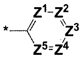
- At least one of A 1 and A 2 includes a moiety represented by the following formula A,
- Z 1 to Z 5 are each independently N or CR a ,
- At least one of Z 1 to Z 5 is N,
- Ra is each independently hydrogen, deuterium, a substituted or unsubstituted C1 to C5 alkyl group, or a substituted or unsubstituted C6 to C18 aryl group,
- R a are each independently present or adjacent groups are linked to form a substituted or unsubstituted aliphatic, aromatic or heteroaromatic monocyclic or polycyclic ring,
- Substituted means that at least one hydrogen is substituted with deuterium, cyano group, C1 to C20 alkyl group, C6 to C30 aryl group, or C2 to C30 heteroaryl group.
- the "substituted" at least one hydrogen is deuterium, C1 to C20.
- Alkyl group C6 to C30 aryl group, pyridinyl group, pyrimidinyl group, triazinyl group, quinolinyl group, isoqui Mean substituted by a nolinyl group, a quinazolinyl group, a benzoquinolinyl group, a benzoisoquinolinyl group, or benzoquinazolinyl.
- the "substituted” means that at least one hydrogen is deuterium, phenyl group, biphenyl group, naphthyl group, pyridinyl group, pyrimidinyl group, triazinyl group, quinolinyl group, isoquinolinyl group, quinazolinyl group, benzoqui Nolinyl group, benzoisoquinolinyl group, or Mean substituted by a benzoquinazolinyl group.
- the present invention provides a compound for an organic optoelectronic device in which an ET unit, that is, a substituent having high electron mobility, is connected to a compound in which benzofuran or benzothiophene is fused to triphenylene, thereby achieving long life, low driving and high efficiency.
- the device can be implemented.
- the glass transition temperature (Tg) is increased to increase the stability of the compound during the process and prevent degradation when applied to the device.
- the glass transition temperature (Tg) may be related to the thermal stability of the compound and the device to which it is applied. That is, the compound for an organic optoelectronic device having a high glass transition temperature (Tg), when applied to the organic light emitting device in the form of a thin film, the temperature in a subsequent process, such as an encapsulat ion process after depositing the compound for the organic optoelectronic device Can be prevented from deteriorating and the lifespan characteristics of the compound and the device can be ensured.
- the LUM0 electron cloud of the ET group can be extended to triphenylene by substituting the ET unit for the triphenylene moiety, so that the LUM0 energy level is relatively lower than that of the compound substituted with the ET group for the benzofuran (or benzothiophene) moiety. Since the polarity of the nitrogen contained in the ET unit can interact with the electrode, it is possible to implement a low driving voltage due to easy charge injection and high mobility.
- a 1 and A 2 are each independently hydrogen, deuterium, a substituted or unsubstituted C6 to C18 aryl group, or a substituted or unsubstituted C2 to C30 heterocyclic group,
- a 1 And A 2 may be represented by Chemical Formula A.
- At least two of Z 1 to Z 5 in Formula A may be N.
- Formula A is specifically represented by Formula A1, Formula A2, Formula A3, and It may be represented by one of formula A4.
- Z 1 , Z 3 , Z 5 , and Z 6 to Z 15 are each independently N or CR a , and at least one of Z 1 , Z 3 , Z 5 , and Z 6 to Z 15 of Formula A1 is N, and At least one of Z 1 and Z 5 of Formulas A2 to A4 is N,
- n are each independently one of an integer of 0 to 2
- R a to R e are each independently hydrogen, deuterium, a substituted or unsubstituted C1 to C5 alkyl group, or a substituted or unsubstituted C6 to C18 aryl group,
- At least two of Z 1 , Z 3 , Z 5 , and Z 6 to Z 15 of Formula A1 may be N.
- At least two of Z 1 and Z 5 of Formulas A2 to A4 may be N.
- Formula A is a phenyl group substituted with an ET unit, a substituted or unsubstituted pyridinyl group, a substituted or unsubstituted pyrimidinyl group, a substituted or unsubstituted triazinyl group, a substituted or unsubstituted quinolinyl group, a substituted or Unsubstituted isoquinolinyl group, substituted or unsubstituted quinazolinyl group, substituted or unsubstituted benzoquinolinyl group, substituted or unsubstituted benzoisoquinolinyl group, or substituted or unsubstituted benzoquinazolinyl group have.
- substituted 11 means that at least one hydrogen is substituted with a phenyl group, a biphenyl group, a naphthyl group, a pyridinyl group, or a pyrimidinyl group.
- the ET unit means an N-containing hexagonal ring-containing moiety except for a carbazolyl group, and includes a pyridinyl group, a pyrimidinyl group, a triazinyl group, a quinolinyl group, an isoquinolinyl group, a quinazolinyl group, and a benzoquinoline Nyl group, benzoisoquinolinyl group, A benzoquinazolinyl group etc. are mentioned. More specifically, it may be a pyrimidinyl group, a triazinyl group, a quinazolinyl group, or a benzoquinazolinyl group.
- Formula A may be selected from substituents listed in Group I below.
- Formula A is a substituted or unsubstituted pyrimidinyl group, a substituted or unsubstituted triazinyl group, a substituted or unsubstituted quinazolinyl group, or a substituted or unsubstituted benzoquinazolinyl It may be a flag. '
- Formula 1 may be represented by, for example, Formula 1-1, or Formula 1- ⁇ .
- a 1 and A 2 in Formulas 1-1 and 1- ⁇ are each independently hydrogen, deuterium, or a substituted or unsubstituted C6 to C18 aryl group .
- L 1 and L 2 may be each independently a single bond, or a substituted or unsubstituted C6 to C20 arylene group, specifically a single bond, or a substituted or unsubstituted C6 to C18 It may be an arylene group, such as a single bond, a substituted or unsubstituted phenylene group, or a substituted or unsubstituted biphenylene group.
- R a may be hydrogen, or a substituted or unsubstituted C6 to C18 aryl group
- R a is each independently present, and Formula 1 may be represented by any one of Formula 1-Al-al, Formula 1-Al_a2, Formula 1-Al-bl, and Formula 1-Al-b2.
- R al to R a4 are each independently hydrogen, deuterium, substituted or unsubstituted C1.
- C5 alkyl group or substituted or unsubstituted C6 to C12 aryl group specifically hydrogen, deuterium, substituted or unsubstituted C1 to C5 alkyl group, or substituted or unsubstituted phenyl group, substituted or unsubstituted biphenyl group
- it may be hydrogen, a phenyl group, or a biphenyl group.
- R a may be connected to adjacent groups to form a substituted or unsubstituted aliphatic, aromatic or heteroaromatic monocyclic or polycyclic ring.
- heteroaromatic polycyclic rings include substituted or unsubstituted quinolinyl groups, substituted or unsubstituted isoquinolinyl groups, substituted or unsubstituted quinazolinyl groups, substituted or unsubstituted benzoquinolines And a phenyl group, a substituted or unsubstituted benzoisoquinolinyl group, a substituted or unsubstituted benzoquinazolinyl group, and the like.
- Examples thereof include the following chemical formulas l-A2-a, formula l-A2-b, formula l_A3_a, and formula l. It may be represented by any one of -A3-b, formula (1-A4-a), and formula (1_A4-b).
- R a to R e are each independently hydrogen, deuterium, a substituted or unsubstituted C1 to C5 alkyl group, or a substituted or unsubstituted C6 to C12 aryl group, Specifically, it may be hydrogen, deuterium, a substituted or unsubstituted C1 to C5 alkyl group, or a substituted or unsubstituted phenyl group, a substituted or unsubstituted biphenyl group, for example, hydrogen, a phenyl group, or a biphenyl group.
- R 1 to R 5 may be hydrogen, deuterium or substituted or unsubstituted C6 to C12 aryl group, specifically, hydrogen, substituted or unsubstituted phenyl group, substituted or unsubstituted biphenyl group Or a substituted or unsubstituted naphthyl group, for example, all may be hydrogen, or either may be a phenyl group or a naphthyl group.
- Compound for an organic optoelectronic device is the formula l-Al-al, Formula l-Al-a2, Formula 1-A1— bl, Formula l-Al-b2, Formula l-A2-a , Formula l-A2-b, Formula l-A4-a, and Formula l_A4-b may be represented by one of the above Formulas, and most particularly, the above Formula l-Al-al, Formula l-Al-a2, Formula l-A2 It may be represented by any one of -a, and the formula 1-A4_a.
- the compound for an organic optoelectronic device represented by Chemical Formula 1 may be selected from, for example, the compounds listed in Group 1, but is not limited thereto.
- the aforementioned compound for organic optoelectronic devices may be applied to organic optoelectronic devices, and may be applied to organic optoelectronic devices alone or in combination with other organic optoelectronic devices.
- the compound for an organic optoelectronic device described above is used together with another compound for an organic optoelectronic device, it may be applied in the form of a composition.
- the compound for an organic optoelectronic device may further include a dopant.
- the dopant may be a red, green or blue dopant.
- the dopant is a material that is lightly mixed to emit light. Materials such as metal complexes that emit light by multiple iple excitat ion ° fl that excite above the triplet state can be used.
- the dopant may be, for example, an inorganic, organic or organic compound, and may be included in one kind or two or more kinds.
- An example of the dopant may be a phosphorescent dopant, and an example of the phosphorescent dopant may be Ir, Pt, 0s, Ti, Zr, Hf, Eu, Tb, Tm, Fe, Co, Ni, Ru, Rh, Pd or the like.
- the organometallic compound containing a combination is mentioned.
- the phosphorescent dopant may be, for example, a compound represented by Chemical Formula Z, but is not limited thereto.
- M is a metal
- L and X are the same or different from each other and a ligand to form a complex with M.
- M may be, for example, Ir, Pt, 0s, Ti, Zr, Hf, Eu, Tb, Tm, Fe, Co, Ni, Ru, Rh, Pd or a combination thereof, wherein L and X are for example bidentate It may be a ligand.
- an organic optoelectronic device may include an anode and a cathode facing each other, and at least one organic layer disposed between the anode and the cathode, and the organic layer may include the compound for an organic optoelectronic device described above. have.
- the organic layer may include a light emitting layer
- the compound for an organic optoelectronic device of the present invention may be included as a host of the light emitting layer, for example, a green host.
- the organic layer may include a light emitting layer and at least one auxiliary layer selected from a hole injection layer, a hole transport layer, an electron blocking layer, an electron transport layer, an electron injection layer, and a hole blocking layer, and the auxiliary layer may be a compound for the organic optoelectronic device. It may include.
- the auxiliary layer may further include an electron transport auxiliary layer adjacent to the emission layer, and the electron transport auxiliary layer may include the compound for the organic optoelectronic device.
- the organic optoelectronic device is not particularly limited as long as the device can switch electrical energy and light energy, and examples thereof include an organic photoelectric device, an organic light emitting device, an organic solar cell, and an organic photosensitive drum.
- FIG. 1 and 2 are cross-sectional views illustrating an organic light emitting diode according to an embodiment.
- an organic light emitting diode 100 includes an anode 120 and a cathode 110 facing each other, and an organic layer 105 positioned between the anode 120 and the cathode 110. Include.
- the anode 120 may be made of, for example, a high work function conductor to facilitate hole injection, for example, metal, metal oxide and / or conductive polymer.
- the anode 120 is, for example, a metal such as nickel, platinum, vanadium, cream, copper, zinc, gold or an alloy thereof; Metal oxides such as zinc oxide, indium oxide, indium tin oxide (IT0), indium zinc oxide (IZ0); Combinations of oxides with metals such as ZnO and A1 or Sn0 2 and Sb; Conductive polymers such as poly (3-methylthiophene), poly (3,4- (ethylene-1,2-dioxy) thiophene) (polyehtylenedioxythiophene: PEDT), polypyrrole and polyaniline, and the like. It is not limited.
- the cathode 110 may be made of a low work function conductor, for example, to facilitate electron injection, and may be made of metal, metal oxide and / or conductive polymer, for example.
- Cathode 110 is, for example magnesium, calcium, sodium, potassium, titanium, indium, yttrium, lithium, gadolinium, aluminum, silver, tin, or metal alloys thereof, such as lead, seseum, barium '; Multilayer structure materials such as, but not limited to, LiF / Al, Li0 2 / Al, LiF / Ca, LiF / Al, and BaF 2 / Ca.
- the organic layer 105 contains the above-mentioned compound for organic optoelectronic devices Light emitting layer 130.
- the organic light emitting diode 200 further includes a hole auxiliary layer 140 in addition to the light emitting layer 130.
- the hole auxiliary layer 140 may further increase hole injection and / or hole mobility between the anode 120 and the light emitting layer 130 and block electrons.
- the hole auxiliary layer 140 may be, for example, a hole transport layer, a hole injection layer, and / or an electron blocking layer, and may include at least one layer.
- the organic layer 105 of FIG. 1 or 2 may further include an electron injection layer, an electron transport layer, an electron transport auxiliary layer, a hole transport layer, a hole transport auxiliary layer, a hole injection layer, or a combination thereof. have.
- the compound for an organic optoelectronic device of the present invention may be included in these organic layers.
- the organic light emitting diodes 100 and 200 may form an anode or a cathode on a substrate, and then may be dried, such as evaporat ion, sputtering plasma plating, or ion plating; or spin coating. After forming an organic layer by a wet film method such as dipping, f low coating, or the like, a cathode or an anode may be formed thereon.
- the above-described organic light emitting device may be applied to an organic light emitting display device. [Form for implementation of invention]
- a compound set forth as more specific examples of the compounds of the present invention was synthesized through the steps ⁇ .
- intermediate 1-2 (27 g, 84.8 ⁇ ol) was dissolved in 0.1 L of chloroform, and then bromine (3.01 g, 18.9 mmol) was added thereto and reacted.
- bromine 3.01 g, 18.9 mmol
- sodium thiosulfate (6.62 g, 41.9 ⁇ ol) saturated in water was added to the reaction solution, and extracted with dichloromethane (DCM), followed by removal of water with anhydrous MgS0 4 , followed by filtration and concentration under reduced pressure. The obtained residue was separated and purified through flash column chromatography to obtain Intermediate 1-3 (21.2 g, 63%).
- An organic light emitting device was manufactured using compound A-1 obtained in Synthesis Example 24 as a host and Ir (PPy) 3 as a dopant.
- IT0 As a positive electrode, IT0 was used at a thickness of 1000 A, and as a negative electrode, aluminum (A1) was used at a thickness of 1000 A.
- the manufacturing method of the organic light emitting device the anode is cut into a size of 50 ⁇ X 50 mm X 0.7 IT IT0 glass substrate having a sheet resistance value of 15 ⁇ / cin 2 in acetone, isopropyl alcohol and pure water After ultrasonic cleaning for 15 minutes each, UV ozone cleaning was used for 30 minutes.
- Bis (2-methyl-8-quinol inolate) -4- (phenylphenol ato) aluminum (BAlq) was deposited on the emission layer to form a hole blocking layer having a thickness of 50 A. Subsequently, Alq 3 was deposited under the same vacuum deposition conditions to form an electron transport layer having a thickness of 200 A.
- An organic photoelectric device was manufactured by sequentially depositing LiF and A1 as a cathode on the electron transport layer.
- the structure of the organic photoelectric device is ⁇ / NPB (80 nm) / EML (Compound A-1 (93 weight%) + Ir (PPy) 3 (7 weight%), 30 nm) / BAlq (5 nm) / Alq3 ( 20 nm) / LiF (1 nm) I Al (100 nm).
- the luminance was measured by using a luminance meter (Minol ta Cs-1000A) while increasing the voltage from 0V to 10V to obtain a result. '
- the current efficiency (cd / A) of the same current density (10 mA / cm 2 ) was calculated using the brightness, current density, and voltage measured from (1) and (2).
- the drive voltage of each device was measured at 15 mA / cm 2 using a current-voltmeter (Kei thley 2400).
- Compound A-72 obtained in Synthesis Example 29 was used as a host, and an organic light emitting diode was manufactured using acetyl acetonat obi s (2-phenyl quinol inato) ir idium (Ir (pq) 2acac) as a dopant.
- IT0 As a positive electrode, IT0 was used at a thickness of 1500 A, and as a negative electrode, aluminum (A1) was used at a thickness of 1000 A.
- the method of manufacturing the organic light emitting device the anode is cut in the size of 50 mm x 50 mm x 0.7 ⁇ glass substrate having a sheet resistance value of 15 ⁇ ⁇ in each of acetone, isopropyl alcohol and pure water. After ultrasonic cleaning for minutes, UV ozone cleaning was used for 30 minutes.
- HT-l N- (biphenyl-4-yl) -N- (4- (9-pheny 1 -9H ⁇ car apelo 1 -3-y 1) phenyl) biphenyl -4-amine
- the phosphorescent dopant acetylacetonatobi s (2-pheny 1 qu i no 1 inato) ir idium (Ir (pq) 2acac) was deposited simultaneously.
- the deposition amount of the phosphorescent dopant was deposited so as to be 7% by weight.
- a bis (2-methyl-8-quinol ino 1 at e) -4- (phenylphenol at o) aluminum (BAlq) was deposited on the light emitting layer using the same vacuum deposition conditions to form a hole blocking layer having a thickness of 50 A. Formed. Subsequently, Tr i s (8-hydroxyquinol inato) aluminum ( ⁇ 1) was deposited under the same vacuum deposition conditions to form an electron transport layer having a thickness of 250 A. An organic photoelectric device was manufactured by sequentially depositing LiF and A1 as a cathode on the electron transport layer.
- the structure of the organic photoelectric device is ⁇ / DNTPD (60 nm) / HT-1 (30 nm) / EML (Compound A-72 (93 weight + Ir (pq) 2 acac (7 weight%), 30 nm) / Balq (5 nm) / Alq 3 (25 nm) / LiF (1 nm) I Al (100 nm).
- An organic light emitting diode was manufactured according to the same method as Example 8 except for using 4, 4′-di (9-carbazol-9-yl) biphenyl (CBP) instead of Compound A-72 of Synthesis Example 29. Rating ⁇
- the present invention may be manufactured in various forms, not limited to the above embodiments, and those skilled in the art to which the present invention pertains may change the technical spirit or essential features of the present invention without changing the technical spirit or essential features of the present invention. It will be appreciated that it may be implemented in a form. Therefore, it should be understood that the embodiments described above are exemplary in all respects and not restrictive.
Landscapes
- Chemical & Material Sciences (AREA)
- Organic Chemistry (AREA)
- Engineering & Computer Science (AREA)
- Materials Engineering (AREA)
- Physics & Mathematics (AREA)
- Spectroscopy & Molecular Physics (AREA)
- Optics & Photonics (AREA)
- Electroluminescent Light Sources (AREA)
- Pyridine Compounds (AREA)
Abstract
화학식 1로 표현되는 유기 광전자 소자용 화합물, 이를 적용한 유기 광전자 소자 및 표시 장치에 관한 것이다. 상기 화학식 1에 대한 상세 내용은 명세서에서 정의한 바와 같다.
Description
【명세서】
【발명의 명칭】
유기 광전자 소자용 화합물, 유기 광전자 소자 및 표시 장치
【기술분야】
유기 광전자 소자용 화합물, 유기 광전자 소자 및 표시 장치에 관한 것이다.
[배경기술】
유기 광전자 소자 (organi c optoelectroni c diode)는 전기 에너지와 광 에너지를 상호 전환할수 있는 소자이다.
유기 광전자 소자는 동작 원리에 따라 크게 두 가지로 나눌 수 있다. 하나는 광 에너지에 의해 형성된 엑시톤 (exci ton)이 전자와 정공으로 분리되고 상기 전자와 정공이 각각 다른 전극으로 전달되면서 전기 에너지를 발생하는 광전 소자이고, 다른 하나는 전극에 전압 또는 전류를 공급하여 전기 에너지로부터 광 에너지를 발생하는 발광 소자이다.
유기 광전자 소자의 예로는 유기 광전 소자, 유기 발광 소자, 유기 태양 전지 및 유기 감광체 드럼 (organi c photo conductor drum) 등을 들 수 있다.
이 중, 유기 발광 소자 (organic l ight emi tt ing diode , OLED)는 근래 평판 표시 장치 ( f lat panel di splay device)의 수요 증가에 따라 크게 주목받고 있다. 상기 유기 발광 소자는 유기 발광 재료에 전류를 가하여 전기 에너지를 빛으로 전환시키는 소자로서, 통상ᅵ 양극 (anode)과 음극 (cathode) 사이에 유기 층이 삽입된 구조로 이루어져 있다. 여기서 유기 층은 발광층과 선택적으로 보조층을 포함할 수 있으며, 상기 보조층은 예컨대 유기발광소자의 효율과 안정성을 높이기 위한 정공 주입 층, 정공 수송 층, 전자 차단 층, 전자 수송 층, 전자 주입 층 및 정공 차단 층에서 선택된 적어도 1층을 포함할수 있다.
유기 발광 소자의 성능은 상기 유기 층의 특성에 의해 영향을 많이 받으며, 그 중에서도 상기 유기 층에 포함된 유기 재료에 의해 영향을 많이 받는다.
특히 상기 유기 발광 소자가 대형 평판 표시 장치에 적용되기 위해서는 정공 및 전자의 이동성을 높이는 동시에 전기화학적 안정성을 높일 수 있는 유기 재료의 개발이 필요하다.
【발명의 상세한 설명】
【기술적 과제】
일 구현예는 고효율 및 장수명 유기 광전자 소자를 구현할 수 있는 유기 광전자 소자용 화합물을 제공한다.
다른 구현예는 상기 화합물을 포함하는 유기 광전자 소자를 제공한다.
또 다른 구현예는 상기 유기 광전자 소자를 포함하는 표시 장치를 제공한다.
【기술적 해결방법】
일 구현예에 따르면, 하기 화학식 1로 표현되는 유기 광전자 소자용 화합물을 제공한다.

상기 화학식 1에서,
X는 0또는 S이고,
R1 내지 R5는 각각 독립적으로 수소, 중수소, 치환 또는 비치환된 C1 내지 C5 알킬기, 또는 치환또는 비치환된 C6 내지 C18 아릴기이고,
L1및 L2는 각각 독립적으로 단일결합,치환또는 비치환된 C6내지 C20 아릴렌기, 또는 치환또는 비치환된 C2 내지 C30 헤테로아릴렌기이고,
A1및 A2는 각각 독립적으로 수소,중수소, 치환 또는 비치환된 C6내지 C18 아릴기, 또는 치환또는 비치환된 C2 내지 C30 헤테로고리기이고,
A1 및 A2 중 적어도 하나는 하기 화학식 A로 표현되는 '모이어티를
포함하고,
[화학식 A]
21 Z2
* // N Z3 상기 화학식 A에서,
Z1 내지 Z5은 각각 독립적으로 N또는 CRa이고,
Z1 내지 Z5 중 적어도 하나는 N이고,
Ra는 각각 독립적으로 수소, 중수소, 치환 또는 비치환된 C1 내지 C5 알킬기, 또는 치환또는 비치환된 C6 내지 C18 아릴기이고,
Ra는 각각 독립적으로 존재하거나 인접한 기끼리 연결되어 치환 또는 비치환된 지방족, 방향족 또는 헤테로방향족의 단환식 또는 다환식 고리를 형성하고,
m 및 n은 각각 독립적으로 0 내지 2의 정수 중 하나이고,
*은 상기 화학식 1의 L1 또는 L2와 연결되는 지점이고,
상기 "치환''이란, 적어도 하나의 수소가 중수소, 시아노기, C1 내지 C20 알킬기, C6 내지 C30 아릴기, 또는 C2 내지 C30 헤테로아릴기로 치환된 것을 의미한다.
다른 구현예에 따르면, 서로 마주하는 양극과 음극, 그리고 상기 양극과 상기 음극사이에 위치하는 적어도 한 층의 유기층을 포함하고, 상기 유기층은 전술한 유기 광전자 소자용 화합물을 포함하는 유기 광전자 소자를 제공한다.
또 다른 구현예에 따르면 상기 유기 광전자 소자를 포함하는 표시 장치를 제공한다.
【발명의 효과】
고효율 장수명 유기 광전자소자를 구현할 수 있다.
【도면의 간단한 설명】
도 1 및 도 2는 일 구현예에 따른 유기 발광 소자를 도시한 단면도이다ᅳ
<부호의 설명 >
100 200 : 유기 발광 소자
105: 유기층
110: o그
百ᅳ 1
120: 이 α:그
ᅳ I
130: 발광층
140: 정공 보조층
【발명의 실시를 위한 최선의 형태】
이하, 본 발명의 구현예를 상세히 설명하기로 한다. 다만, 이는 예시로서 제시되는 것으로, 이에 의해 본 발명이 제한되지는 않으며 본 발명은 후술할 청구범위의 범주에 의해 정의될 뿐이다.
본 명세서에서 "치환1 '이란 별도의 정의가 없는 한, 치환기 또는 화합물 중의 적어도 하나의 수소가중수소, 할로겐기, 히드록실기, 아미노기, 치환 또는 비치환된 C1 내지 C30 아민기, 니트로기, 치환 또는 비치환된 C1 내지 C40실릴기, C1내지 C30 알킬기, C1내지 C10 알킬실릴기, C6내지 C30 아릴실릴기, C3내지 C30시클로알킬기, C3내지 C30헤테로시클로알킬기, C6 내지 C30아릴기 , C2내지 C30헤테로아릴기, C1내지 C20 알콕시기, C1내지 C10 트리플루오로알킬기, 시아노기, 또는 이들의 조합으로 치환된 것을 의미한다.
본 발명의 일 예에서, "치환"은 치환기 또는 화합물 중의 적어도 하나의 수소가중수소 , C1내지 C30알킬기, C1내지 C10알킬실릴기, C6내지 C30아릴실릴기 C3내지 C30시클로알킬기 , C3내지 C30헤테로시클로알킬기, C6 내지 C30 아릴기, C2 내지 C30 헤테로아릴기로 치환된 것을 의미한다. 또한, 본 발명의 구체적인 일 예에서, "치환 "은 치환기 또는 화합물 중의 적어도 하나의 수소가 중수소, C1내지 C20알킬기, C6내지 C30아릴기 또는 C2 내지 C30 헤테로아릴기로 치환된 것을 의미한다. 또한, 본 발명의 구체적인 일 예에서, "치환 "은 치환기 또는 화합물 중의 적어도 하나의 수소가 중수소, C1 내지 C5 알킬기, C6 내지 C18 아릴기, 피리디닐기, 피리미디닐기, 트리아지닐기, 퀴놀리닐기, 이소퀴놀리닐기, 퀴나졸리닐기, 벤조퀴놀리닐기, 벤조이소퀴놀리닐기, 또는 벤조퀴나졸리닐기로 치환된 것을
의미한다. 또한, 본 발명의 구체적인 일 예에서, "치환 "은 치환기 또는 화합물 중의 적어도 하나의 수소가 중수소, 메틸기, 에틸기, 프로판일기, 부틸기, 페닐기, 바이페닐기, 터페닐기, 나프틸기, 트리페닐기, 피리디닐기, 피리미디닐기, 트리아지닐기, 퀴놀리닐기, 이소퀴놀리닐기, 퀴나졸리닐기, 벤조퀴놀리닐기, 벤조이소퀴놀리닐기, 또는 벤조퀴나졸리닐기로 치환된 것을 의미한다.
본 명세서에서 "헤테로 "란 별도의 정의가 없는 한, 하나의 작용기 내에 N, 0, S, P및 Si로 이루어진 군에서 선택되는 헤테로 원자를 1내지 3개 함유하고, 나머지는 탄소인 것을 의미한다.
본 명세서에서 "알킬 (alkyl )기' '이란 별도의 정의가 없는 한, 지방족 탄화수소기를 의미한다. 알킬기는 어떠한 이중결합이나 삼중결합을 포함하고 있지 않은 "포화 알킬 (saturated alkyl )기' '일 수 있다.
상기 알킬기는 C1 내지 C30인 알킬기일 수 있다. 보다 구체적으로 알킬기는 C1 내지 C20 알킬기 또는 C1 내지 C10 알킬기일 수도 있다. 예를 들어, C1내지 C4알킬기는 알킬쇄에 1내지 4개의 탄소원자가 포함되는 것을 의미하며, 메틸, 에틸, 프로필, 이소-프로필, n-부틸, 이소-부틸, sec-부틸 및 t-부틸로 이루어진 군에서 선택됨을 나타낸다.
상기 알킬기는 구체적인 예를 들어 메틸기, 에틸기, 프로필기, 이소프로필기 부틸기, 이소부틸기, t-부틸기, 펜틸기, 핵실기, 시클로프로필기, 시클로부틸기, 시클로펜틸기, 시클로핵실기 등을 의미한다. 본 명세서에서 "아릴 (aryl )기''는 탄화수소 방향족 모이어티를 하나 이상 갖는 그룹을 총괄하는 개념으로서 ,
탄화수소 방향족 모이어티의 모든 원소가 P-오비탈을 가지면서, 이들 p_오비탈이 공액 (conjUgat i0n)을 형성하고 있는 형태, 예컨대 페닐기, 나프틸기 등을 포함하고,
2이상의 탄화수소 방향족 모이어티들이 시그마 결합을 통하여 연결된 형태, 예컨대 바이페닐기, 터페닐기, 쿼터페닐기 등을 포함하며,
2 이상의 탄화수소 방향족 모이어티들이 직접 또는 간접적으로 융합된 비방향족 융합 고리도 포함할 수 있다. 예컨대, 플루오레닐기 등을 들 수
있다.
아릴기는 모노시클릭, 폴리시클릭 또는 융합 고리 폴리시클릭 (즉, 탄소원자들의 인접한 쌍들을 나워 가지는 고리) 작용기를 포함한다.
본 명세서에서 "헤테로고리기 (heterocycl i c group) "는 헤테로아릴기를 포함하는 상위 개념으로서, 아릴기, 시클로알킬기, 이들의 융합고리 또는 이들의 조합과 같은 고리 화합물 내에 탄소 (C) 대신 N, 0, S , P 및 Si로 이루어진 군에서 선택되는 헤테로 원자를 적어도 한 개를 함유하는 것을 의미한다. 상기 헤테로고리기가 융합고리인 경우, 상기 헤테로고리기 전체 또는 각각의 고리마다 헤테로 원자를 한 개 이상 포함할 수 있다.
일 예로 "헤테로아릴 (heteroaryl )기1'는 아릴기 내에 N , 0, S, P 및
Si로 이루어진 군에서 선택되는 헤테로 원자를 적어도 한 개를 함유하는 것을 의미한다. 2 이상의 헤테로아릴기는 시그마 결합을 통하여 직접 연결되거나, 상기 헤테로아릴기가 2 이상의 고리를 포함할 경우, 2 이상의 고리들은 서로 융합될 수 있다. 상기 헤테로아릴기가 융합고리인 경우, 각각의 고리마다상기 헤테로 원자를 1 내지 3개 포함할 수 있다.
상기 헤테로고리기는 구체적인 예를 들어, 피리디닐기, 피리미디닐기, 피라지닐기, 피리다지닐기, 트리아지닐기, 퀴놀리닐기, 이소퀴놀리닐기, 퀴나졸리닐기, 벤조퀴놀리닐기, 벤조이소퀴놀리닐기, 벤조퀴나졸리닐기 등을 포함할 수 있다.
보다 구체적으로, 치환 또는 비치환된 C6 내지 C30 아릴기 및 /또는 치환또는 비치환된 C2내지 C30헤테로고리기는, 치환또는 비치환된 페닐기 , 치환또는 비치환된 나프틸기, 치환 또는 비치환된 안트라세닐기, 치환또는 비치환된 페난트레닐기, 치환 또는 비치환된 나프타세닐기, 치환 또는 비치환된 피레닐기, 치환 또는 비치환된 바이페닐기, 치환 또는 비치환된 P-터페닐기, 치환 또는 비치환된 m-터페닐기, 치환 또는 비치환된 0-터페닐기, 치환 또는 비치환된 크리세닐기, 치환 또는 비치환된 트리페닐렌기, 치환 또는 비치환된 페릴레닐기, 치환 또는 비치환된 플루오레닐기, 치환또는 비치환된 인데닐기, 치환 또는 비치환된 퓨라닐기, 치환 또는 비치환된 티오페닐기, 치환 또는 비치환된 피를릴기, 치환 또는
비치환된 피라졸릴기, 치환 또는 비치환된 이미다졸일기, 치환 ΪΧ느
τ 비치환된 트리아졸일기, 치환 또는 비치환된 옥사졸일기, 치환 ΤΧ느 비치환된 티아졸일기, 치환 또는 비치환된 옥사디아졸일기, 치환 CJ 느 비치환된 티아디아졸일기, 치환 또는 비치환된 피리딜기, 치환 t :느ᄂ_ 비치환된 피리미디닐기, 치환 또는 비치환된 피라지닐기, 치환 댜느 비치환된 트리아지닐기, 치환 또는 비치환된 벤조퓨라닐기, 치환 IX느 비치환된 벤조티오페닐기, 치환또는 비치환된 벤즈이미다졸일기, 치환 또는 비치환된 인돌일기, 치환 또는 비치환된 퀴놀리닐기, 치환 또는 비치환된 이소퀴놀리닐기, 치환 또는 비치환된 퀴나졸리닐기, 치환 또는 비치환된 퀴나졸리닐기, 치환 또는 비치환된 벤조퀴놀리닐기, 치환 또는 비치환된 벤조이소퀴놀리닐기, 치환 또는 비치환된 벤조퀴나졸리닐기, 치환 또는 비치환된 나프티리디닐기, 치환 또는 비치환된 벤즈옥사진일기, 치환 또는 비치환된 벤즈티아진일기 치환 또는 비치환된 아크리디닐기, 치환 또는 비치환된 페나진일기, 치환 또는 비치환된 페노티아진일기, 치환 또는 비치환된 페녹사진일기, 치환 또는 비치환된 디벤조퓨란일기, 또는 치환 또는 비치환된 디벤조티오펜일기, 또는 이들의 조합일 수 있으나, 이에 제한되지는 않는다.
이하 일 구현예에 따른 유기 광전자 소자용 화합물을 설명한다.
ᅳ 일 구현예에 따른 유기 광전자 소자용 화합물은 하기 화학식 1로 표현된다.

상기 화학식 1에서,
X는 0또는 S이고,
R1 내지 R5는 각각 독립적으로 수소, 중수소, 치환 또는 비치환된 C1
내지 C5 알킬기, 또는 치환또는 비치환된 C6 내지 C18 아릴기이고,
L1및 L2는 각각 독립작으로 단일결합,치환또는 비치환된 C6내지 C20 아릴렌기, 또는 치환또는 비치환된 C2 내지 C30 헤테로아릴렌기이고,
A1및 A2는 각각 독립적으로 수소, 중수소, 치환또는 비치환된 C6내지 C18 아릴기, 또는 치환또는 비치환된 C2 내지 C30 헤테로고리기이고,
A1 및 A2 중 적어도 하나는 하기 화학식 A로 표현되는 모이어티를 포함하고,
[화학식 A]
*ᅳ 、 3 상기 화학식 A에서,
Z1 내지 Z5은 각각 독립적으로 N또는 CRa이고,
Z1 내지 Z5 중 적어도 하나는 N이고,
Ra는 각각 독립적으로 수소, 중수소, 치환 또는 비치환된 C1 내지 C5 알킬기, 또는 치환 또는 비치환된 C6 내지 C18 아릴기이고,
Ra는 각각 독립적으로 존재하거나 인접한 기끼리 연결되어 치환 또는 비치환된 지방족, 방향족 또는 헤테로방향족의 단환식 또는 다환식 고리를 형성하고,
*은 상기 화학식 1의 L1또는 L2와 연결되는 지점이고,
상기 "치환"이란, 적어도 하나의 수소가 중수소, 시아노기, C1 내지 C20 알킬기, C6 내지 C30 아릴기, 또는 C2 내지 C30 헤테로아릴기로 치환된 것을 의미한다. 본 발명의 구체적인 일예에서, 상기 "치환 "이란, 적어도 하나의 수소가 중수소, C1내지 C20.알킬기, C6내지 C30아릴기, 피리디닐기, 피리미디닐기, 트리아지닐기, 퀴놀리닐기, 이소퀴놀리닐기, 퀴나졸리닐기, 벤조퀴놀리닐기, 벤조이소퀴놀리닐기, 또는 벤조퀴나졸리닐로 치환된 것을 의미한다.
예컨대, 상기 "치환"이란, 적어도 하나의 수소가 중수소, 페닐기, 바이페닐기,나프틸기,피리디닐기,피리미디닐기,트리아지닐기,퀴놀리닐기, 이소퀴놀리닐기, 퀴나졸리닐기, 벤조퀴놀리닐기, 벤조이소퀴놀리닐기, 또는
벤조퀴나졸리닐기로 치환된 것을 의미한다.
본 발명은 트리페닐렌에 벤조퓨란 또는 벤조티오펜이 융합된 화합물에 ET유닛 (Electron transfer uni t ) , 즉 전자 이동도가높은 치환기가 연결된 유기 광전자 소자용 화합물을 제공함으로써 장수명, 저구동 및 고효율의 소자를 구현할 수 있다.
본 발명에 따른 화합물은 트리페닐렌에 벤조퓨란 또는 벤조티오펜이 융합됨으로써, 유리전이온도 (Tg)가높아져 소자에 적용 시 공정 중 화합물의 안정성을 높이고 열화를 방지할 수 있다. 유리전이온도 (Tg)는 화합물 및 이를 적용한 소자의 열안정성과 관련될 수 있다. 즉 높은 유리전이온도 (Tg)를 가지는 유기 광전자 소자용 화합물은, 유기발광소자에 박막 형태로 적용되었을 때, 상기 유기 광전자 소자용 화합물을 증착한후에 이루어지는 후속 공정 , 예컨대 봉지 (encapsulat ion) 공정에서 온도에 의해 열화되는 것이 방지되어 화합물 및 소자의 수명 특성을 확보할 수 있다. 또한, ET 유닛이 트리페닐렌 모이어티에 치환됨으로써 ET기의 LUM0 전자 구름이 트리페닐렌까지 확장될 수 있으므로, 벤조퓨란 (또는 벤조티오펜) 모이어티에 ET기가 치환된 화합물 대비 상대적으로 낮은 LUM0 에너지 레벨을 가질 수 있고, ET 유닛에 포함된 질소의 극성기로 인하여 전극과 상호작용이 가능하기 때문에 전하의 주입이 용이하고 이동도가 높음으로 인하여 저구동 전압을 구현할 수 있다.
뿐만 아니라, 분자 구조의 입체 장해성으로 인하여 분자 사이의 상호 작용이 작아져 결정화가 억제되므로, 이를 포함하는 유기 EL 소자의 수율 향상 및 장수명의 효과를 확보할 수 있다.
본 발명의 일 실시예에서, 상기 A1 및 A2는 각각 독립적으로 수소, 중수소, 치환 또는 비치환된 C6 내지 C18 아릴기, 또는 치환 또는 비치환된 C2내지 C30헤테로고리기일 수 있고 , Α1및 Α2중 적어도 하나가상기 화학식 Α로 표현될 수 있다.
본 발명의 일 실시예에서, 화학식 A에서 Z1 내지 Z5 중 적어도 두개는 N일 수 있다.
상기 화학식 A는 구체적으로 하기 화학식 A1 ,화학식 A2 , 화학식 A3및
화학식 A4 중 하나로 표현될 수 있다.
[화학식 A1] [화학식 A2] [화학식 A3] [화학식 A4]

상기 화학식 Al 내지 화학식 A4에서,
Z1 , Z3 , Z5 , 및 Z6 내지 Z15은 각각 독립적으로 N또는 CRa이고, 상기 화학식 A1의 Z1 , Z3 , Z5 , 및 Z6 내지 Z15중 적어도 하나는 N이고, 상기 화학식 A2 내지 A4의 Z1 및 Z5 중 적어도 하나는 N이고,
m 및 n은 각각 독립적으로 0 내지 2의 정수 중 하나이고,
Ra 내지 Re는 각각 독립적으로 수소, 중수소, 치환 또는 비치환된 C1 내지 C5 알킬기 또는 치환또는 비치환된 C6 내지 C18 아릴기이고,
*은 상기 화학식 1의 L1또는 L2와 연결되는 지점이다.
본 발명의 구체적인 일 실시예에서 ,상기 화학식 A1의 Z1 , Z3 , Z5 ,및 Z6 내지 Z15 중 적어도 둘은 N일 수 있다. 、
본 발명의 구체적인 다른 일 실시예에서 ,상기 화학식 A2내지 A4의 Z1 및 Z5 중 적어도 둘은 N일 수 있다.
상기 화학식 A는 예컨대 ET 유닛으로 치환된 페닐기, 치환 또는 비치환된 피리디닐기, 치환 또는 비치환된 피리미디닐기, 치환 또는 비치환된 트리아지닐기, 치환 또는 비치환된 퀴놀리닐기, 치환 또는 비치환된 이소퀴놀리닐기, 치환 또는 비치환된 퀴나졸리닐기, 치환 또는 비치환된 벤조퀴놀리닐기, 치환 또는 비치환된 벤조이소퀴놀리닐기, 또는 치환 또는 비치환된 벤조퀴나졸리닐기일 수 있다. 이 때 "치환 11이란, 적어도 하나의 수소가 페닐기, 바이페닐기, 나프틸기, 피리디닐기, 또는 피리미디닐기로 치환된 것을 의미한다.
한편, ET유닛이란 카바졸일기를 제외한 N함유 6각환 함유 모이어티를 의미하는 것으로서, 피리디닐기, 피리미디닐기, 트리아지닐기, 퀴놀리닐기, 이소퀴놀리닐기, 퀴나졸리닐기, 벤조퀴놀리닐기, 벤조이소퀴놀리닐기,
벤조퀴나졸리닐기 등을 들 수 있다. 보다 구체적으로, 피리미디닐기, 트리아지닐기, 퀴나졸리닐기 또는 벤조퀴나졸리닐기 일 수 있다.
본 발명의 구체적인 일 실시예에서, 상기 화학식 A는 하기 그룹 I에 나열된 치환기에서 선택될 수 있다.
[그룹 I
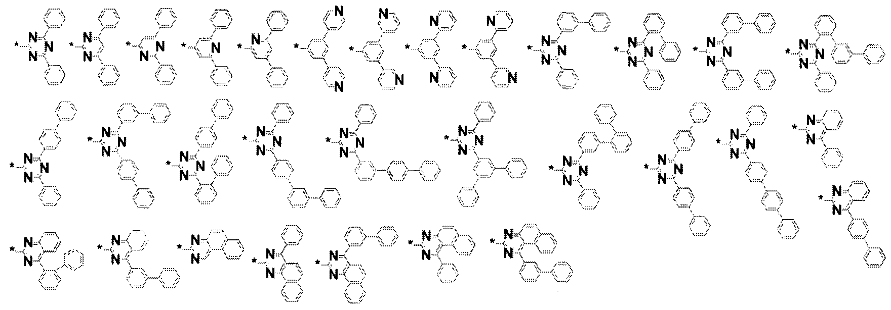
상기 그룹 I에서 , *은 상기 화학식 1의 L1 또는 L2와 연결되는 지점이다.
본 발명의 가장 구체적인 일 실시예에서 상기 화학식 A는 치환 또는 비치환된 피리미디닐기, 치환 또는 비치환된 트리아지닐기, 치환 또는 비치환된 퀴나졸리닐기, 또는 치환 또는 비치환된 벤조퀴나졸리닐기일 수 있다. '
한편, 화학식 A의 치환 위치에 따라 상기 화학식 1은 예컨대 하기 화학식 1- 1, 또는 화학식 1- Π로 표현될 수 있다.
[ 1- 1

상기 화학식 1- I ,및 화학식 l- Π에서, Α1및 X, Z1내지 l\ R1내지 그리고 L1 및 L2은 전술한 바와 같고,
상기 화학식 1- 1, 및 화학식 1- Π의 A1및 A2는 각각 독립적으로 수소, 중수소, 또는 치환 또는 비치환된 C6 내지 C18 아릴기일. 수 있다.
구체적으로, 수소, 중수소, 치환 또는 비치환된 페닐기, 치환 또는 비치환된 바이페닐기, 또는 치환또는 비치환된 나프틸기일 수 있고, 더욱 구체적으로 수소 또는 페닐기일 수 있다.
본 발명의 일 실시예에서, 상기 L1및 L2는 각각 독립적으로 단일결합, 또는 치환 또는 비치환된 C6 내지 C20 아릴렌기일 수 있고, 구체적으로 단일결합, 또는 치환 또는 비치환된 C6 내지 C18 아릴렌기일 수 있으며, 예컨대 단일결합, 치환 또는 비치환된 페닐렌기, 또는 치환 또는 비치환된 바이페닐렌기일 수 있다.
본 발명의 구체적인 일 실시예에서, 상기 Ra는 수소, 또는 치환 또는 비치환된 C6 내지 C18 아릴기일 수 있고,
Ra는 각각 독립적으로 존재하여 상기 화학식 1은 예컨대 하기 화학식 1-Al-al , 화학식 1-Al_a2, 화학식 1-Al-bl, 및 화학식 l-Al-b2 중 어느 하나로 표현될 수 있다.

상기 화학식 화학식 1-Al-al, 화학식 l_Al-a2, 화학식 l-Al-bl , 및 화학식 l-Al-b2에서, X, L1 및 L2, R1 내지 R5, m 및 n은 전술한 바와 같고, Ral 내지 Ra4는 각각 독립적으로 수소, 중수소, 치환또는 비치환된 C1
내지 C5 알킬기, 또는 치환 또는 비치환된 C6 내지 C12 아릴기이고, 구체적으로 수소, 중수소, 치환 또는 비치환된 C1내지 C5알킬기, 또는 치환 또는 비치환된 페닐기, 치환 또는 비치환된 바이페닐기일 수 있으며, 예컨대 수소, 페닐기, 또는 바이페닐기일 수 있다.
또한, Ra는 인접한 기끼리 연결되어 치환 또는 비치환된 지방족, 방향족 또는 헤테로방향족의 단환식 또는 다환식 고리를 형성할 수 있다.
"인접한 기끼리 연결1 '되는 경우란, Ra가 연결된 페닐기와 Ra 중 인접하고 있는 어느 2개의 치환기가 서로 융합하여 치환 또는 비치환된 지방족, 방향족 또는 헤테로방향족의 단환식 또는 다환식 고리를 형성하는 것을 의미한다. 헤테로방향족 다환식 고리의 예로는 치환 또는 비치환된 퀴놀리닐기, 치환 또는 비치환된 이소퀴놀리닐기, 치환 또는 비치환된 퀴나졸리닐기, 치환 또는 비치환된 벤조퀴놀리닐기, 치환 또는 비치환된 벤조이소퀴놀리닐기, 치환 또는 비치환된 벤조퀴나졸리닐기 등을 들 수 있으며, 예컨대 하기 화학삭 l-A2-a, 화학식 l-A2-b, 화학식 l_A3_a, 화학식 l-A3-b, 화학식 l-A4-a, 및 화학식 l_A4-b 중 어느 하나로 표현될 수 있다.
[화학식 l-A2-a] [화학식 1— A2-b] [화학식 -A3-a]

상기 화학식 l-A2-a, 화학식 l-A2-b, 화학삭 1-A3_a, 화학식 l_A3_b, 화학식 l-A4-a, 및 화학식 l-A4-b에서, X, L1 및 L2, 그리고 R1 내지 R5는 전술한 바와 같고,
Ra 내지 Re는 각각 독립적으로 수소, 중수소, 치환 또는 비치환된 C1 내지 C5 알킬기, 또는 치환 또는 비치환된 C6 내지 C12 아릴기이고,
구체적으로 수소, 중수소, 치환또는 비치환된 C1내지 C5알킬기, 또는 치환 또는 비치환된 페닐기, 치환또는 비치환된 바이페닐기일 수 있으며, 예컨대, 수소, 페닐기, 또는 바이페닐기일 수 있다.
본 발명의 일 실시예에서, R1내지 R5는 수소, 중수소 또는 치환또는 비치환된 C6 내지 C12 아릴기일 수 있고, 구체적으로, 수소, 치환 또는 비치환된 페닐기, 치환또는 비치환된 바이페닐기, 또는 치환또는 비치환된 나프틸기일 수 있으며, 예컨대, 모두 수소이거나 어느 하나가 페닐기 또는 나프틸기일 수 있다.
본 발명의 구체적인 일 실시예에 따른 유기 광전자 소자용 화합물은 상기 화학식 l-Al-al , 화학식 l-Al-a2, 화학식 1-A1— bl , 화학식 l-Al-b2 , 화학식 l-A2-a, 화학식 l-A2-b, 화학식 l-A4-a, 및 화학식 l_A4-b 중 어느 하나로 표현될 수 있고, 가장 구체적으로 상기 화학식 l-Al-al, 화학식 l-Al-a2, 화학식 l-A2-a, 및 화학식 1-A4_a 중 어느 하나로 표현될 수 있다. 상기 화학식 1로 표현되는 유기 광전자 소자용 화합물은 예컨대 하기 그룹 1에 나열된 화합물에서 선택될 수 있으나, 이에 한정되는 것은 아니다.
[그룹 1]

[A-16] [A-17] [A-18] [A— 19] [A-20]

[A-47] [A-48] [A-49] [A-50] [A-51]

[A-76] [A— 77] [A-78] [A-79] [A-80]
 //:/ O s-6900ZJ0SMl>d8Ϊ0ΖAV


상기 유기 광전자 소자용 화합물은 도펀트를 더 포함할 수 있다. 상기 도펀트는 적색, 녹색 또는 청색의 도편트일 수 있다.
상기 도펀트는 미량 흔합되어 발광을 일으키는 물질로, 일반적으로
삼중항 상태 이상으로 여기시키는 다중항 여기 (mult iple excitat ion)°fl 의해 발광하는 금속 착체 (metal complex)와 같은 물질이 사용될 수 있다. 상기 도펀트는 예컨대 무기,유기,유무기 화합물일 수 있으며, 1종 또는 2종 이상 포함될 수 있다.
상기 도펀트의 일 예로 인광 도펀트를 들 수 있으며, 인광 도편트의 예로는 Ir , Pt , 0s , Ti , Zr , Hf , Eu, Tb, Tm, Fe , Co, Ni, Ru, Rh, Pd또는 이들의 조합을 포함하는 유기 금속화합물을 들 수 있다. 상기 인광 도펀트는 예컨대 하기 화학식 Z로 표현되는 화합물을 사용할 수 있으나, 이에 한정되는 것은 아니다.
[화학식 Z]
L2MX
상기 화학식 Z에서, M은 금속이고, L 및 X는 서로 같거나 다르며 M과 착화합물을 형성하는 리간드이다.
상기 M은 예컨대 Ir , Pt , 0s , Ti , Zr , Hf , Eu, Tb, Tm, Fe , Co , Ni , Ru, Rh, Pd 또는 이들의 조합일 수 있고, 상기 L 및 X는 예컨대 바이덴테이트 리간드일 수 있다.
이하 전술한 유기 광전자 소자용 화합물을 적용한 유기 광전자 소자를 설명한다.
또 다른 구현예에 따른 유기 광전자 소자는 서로 마주하는 양극과 음극, 그리고 상기 양극과 상기 음극 사이에 위치하는 적어도 한 층의 유기층을 포함하고, 상기 유기층은 전술한 유기 광전자 소자용 화합물을 포함할 수 있다.
일 예로 상기 유기층은 발광층을 포함하고, 본 발명의 유기 광전자 소자용 화합물은 상기 발광층의 호스트, 예컨대 그린 호스트로서 포함될 수 있다.
또한, 상기 유기층은 발광층, 및 정공주입층, 정공수송층, 전자차단층, 전자수송층, 전자주입층 및 정공차단층에서 선택된 적어도 하나의 보조층을 포함하고, 상기 보조층은 상기 유기 광전자 소자용 화합물을 포함할 수 있다.
상기 보조층은 발광층에 인접한 전자수송보조층을 더 포함하고, 상기 전자수송보조층은 상기 유기 광전자소자용 화합물을 포함할 수 있다.
상기 유기 광전자 소자는 전기 에너지와 광 에너지를 상호 전환할 수 있는 소자이면 특별히 한정되지 않으며, 예컨대 유기 광전 소자, 유기 발광 소자, 유기 태양 전지 및 유기 감광체 드럼 등을 들 수 있다.
여기서는 유기 광전자 소자의 일 예인 유기 발광 소자를 도면을 참고하여 설명한다.
도 1 및 도 2는 일 구현예에 따른 유기 발광 소자를 보여주는 단면도이다.
도 1을 참고하면, 일 구현예에 따른 유기 발광 소자 (100)는 서로 마주하는 양극 (120)과 음극 (110), 그리고 양극 (120)과 음극 (110) 사이에 위치하는 유기층 (105)을 포함한다.
양극 (120)은 예컨대 정공 주입이 원활하도록 일 함수가 높은 도전체로 만들어질 수 있으며, 쎄컨대 금속, 금속 산화물 및 /또는 도전성 고분자로 만들어질 수 있다. 양극 (120)은 예컨대 니켈, 백금, 바나듐,크름, 구리 , 아연, 금과 같은 금속 또는 이들의 합금; 아연산화물, 인듐산화물, 인듐주석산화물 ( IT0) , 인듐아연산화물 ( IZ0)과 같은 금속 산화물; ZnO와 A1 또는 Sn02와 Sb와 같은 금속과 산화물의 조합; 폴리 (3-메틸티오펜), 폴리 (3,4- (에틸렌 -1 , 2-디옥시 )티오펜) (polyehtylenedioxythiophene : PEDT), 폴리피를 및 폴리아닐린과 같은 도전성 고분자 등을 들 수 있으나, 이에 한정되는 것은 아니다.
음극 (110)은 예컨대 전자 주입이 원활하도록 、일 함수가 낮은 도전체로 만들어질 수 있으며, 예컨대 금속, 금속 산화물 및 /또는 도전성 고분자로 만들어질 수 있다. 음극 (110)은 예컨대 마그네슘, 칼슘, 나트륨, 칼륨,타이타늄, 인듐, 이트륨,리튬,가돌리늄, 알루미늄,은,주석,납,세슴, 바륨 등과 같은 금속 또는 이들의 합금'; LiF/Al , Li02/Al , LiF/Ca, LiF/Al 및 BaF2/Ca과 같은 다층 구조 물질을 들 수 있으나, 이에 한정되는 것은 아니다ᅳ
유기층 (105)은 전술한 유기 광전자 소자용 화합물을 포함하는
발광층 ( 130)을 포함한다.
도 2는 다른 구현예에 따른 유기 발광소자를 보여주는 단면도이다. 도 2를 참고하면, 유기 발광 소자 (200)는 발광층 (130) 외에 정공 보조층 ( 140)을 더 포함한다. 정공 보조층 ( 140)은 양극 ( 120)과 발광층 ( 130) 사이의 정공 주입 및 /또는 정공 이동성을 더욱 높이고 전자를 차단할 수 있다. 정공 보조층 ( 140)은 예컨대 정공 수송층, 정공 주입층 및 /또는 전자 차단층일 수 있으며, 적어도 1층을 포함할 수 있다.
도 1 또는 도 2의 유기층 ( 105)은 도시하지는 않았지만, 전자주입층, 전자수송층, 전자수송보조층, 정공수송층, 정공수송보조층, 정공주입층 또는 이들의 조합층을 추가로 더 포함할 수 있다. 본 발명의 유기 광전자 소자용 화합물은 이들 유기층에 포함될 수 있다. 유기 발광 소자 ( 100, 200)는 기판 위에 양극 또는 음극을 형성한 후, 진공증착법 (evaporat ion) , 스퍼터링 (sput ter ing 플라즈마 도금 및 이온도금과 같은 건식성막법 ; 또는 스핀코팅 (spin coat ing) , 침지법 (dipping) , 유동코팅법 ( f low coat ing)과 같은 습식성막법 등으로 유기층을 형성한 후, 그 위에 음극 또는 양극을 형성하여 제조할수 있다.
전술한유기 발광 소자는 유기 발광 표시 장치에 적용될 수 있다. 【발명의 실시를 위한 형태】
이하에서는 본 발명의 구체적인 실시예들을 제시한다. 다만, 하기에 기재된 실시예들은 본 발명을 구체적으로 예시하거나 설명하기 위한 것에 불과하며, 이로서 본 발명이 제한되어서는 아니된다.
이하, 실시예 및 합성예에서 사용된 출발물질 및 반웅물질은 특별한 언급이 없는 한, Sigma-Aldr i ch 社 또는 TCI 社에서 구입하였거나, 공지된 방법을 통해 합성하였다.
(유기 광전자소자용화합물의 제조)
본 발명의 화합물의 보다 구체적인 예로서 제시된 화합물을 하기 ■ 단계를 통해 합성하였다.
(제 1유기 광전자소자용화합물)
합성예 1: 증간체 1-1의 합
 질소 환경에서 tokyo chemical industry(hUp://w .tci chemicals .com/)사에서 구입한 d i benzo fur an-4-bor on i c acid(50 g, 236 隱 ol)을 tetrahydrofuran(THF) 0.8 L에 녹인 후, 여기에 Mascot (Asia) Company Limited에서 구입한 2,2'-dibromobiphenyl(110 g, 354 醒 ol)와 tetrakis(triphenylphosphine)pal ladium(2.72 g, 2.86 mmol)을 넣고 교반시켰다. 물에 포화된 potassuim carbonate(81.5 g, 59.0 隱 ol)을 넣고 80 °C에서 12시간 동안 가열하여 환류 시켰다. 반웅 완료 후 반웅액에 물을 넣고 dichloromethane(DCM)로 추출한 다음 무수 MgS04로 수분을 제거한 후, 필터하고 감압 농축하였다. 이렇게 얻어진 잔사를 flash column chromatography로 분리 정제하여 중간체 1-1(49.7 g, 53 %)를 얻었다.
HRMS (70 eV, EI+): m/z calcd for C24H15BK): 398.0306, found: 398.
Elemental Analysis: C, 72 ; H, 4 % 합성예 2: 중간체 1-2의 합성

1-1 I -2
질소 환경에서 중간체 1-1(50 g, 236誦 ol)을 xylene 0.5 L에 녹인 후, 여기에 bis(dibenzyl ideneacetone)pal ladium(0)(3.48 g, 6.05 隱 ol)와 triphenylphosphine(6.35 g, 2.42 mmol )그리고 cesium carbonate(47.3 g, 145 mmol)을 넣고 140 °C에서 27시간 동안 가열하여 환류 시켰다. 반응 완료 후
반웅액에 물을 넣고 dichloromethane(DCM)로 추출한 다음 무수 MgS04로 수분을 제거한 후, 필터하고 감압 농축하였다. 이렇게 얻어진 잔사를 flash column chromatography로 분리 정제하여 중간체 1-2(27.6 g, 72 %)를 얻었다.
HRMS (70 eV, EI+): m/z calcd for C24H140: 318.1045, found: 318. Elemental Analysis: C, 91 ; H, 4 %

1 -2 1 -3
질소 환경에서 중간체 1-2(27 g, 84.8 隱 ol)을 chloroform 0.1 L에 녹인 후, 여기에 bromine(3.01 g, 18.9mmol)올 넣고 반웅 시켰다. 반웅 완료 후 반웅액에 물에 포화된 sodium thiosulfate(6.62 g, 41.9 腿 ol) 넣고 dichloromethane(DCM)로 추출한 다음 무수 MgS04로 수분을 제거한 후, 필터하고 감압 농축하였다. 이렇게 얻어진 잔사를 flash column chromatography로 분리 정제하여 중간체 1-3(21.2 g, 63 %)를 얻었다.
HRMS (70 eV, EI+): m/z calcd for C24H13BrO: 396.0150, found: 396.
Elemental Analysis: C, 73 %; H, 3 %

질소 환경에서 중간체 I-3(20g, 50.3隱 ol)을 dimethyl foramide(DMF) 0.6 L에 녹인 후, 여기에 bis(pinacolato)diboron (15.3 g, 60.4 隱 ol)와 (1, -bis (diphenylphosphine)f err ocene)dichl or opal ladium(II) (0.41 g, 0.5
睡 ol) 그리고 potassium acetate(14.8 g, 151瞧 ol)을 넣고 150 °C에서 3시간 동안 가열하여 환류 시켰다. 반응 완료 후 반웅액에 물을 넣고 흔합물을 필터한 후, 진공오븐에서 건조하였다. 이렇게 얻어진 잔사를 flash column chromatography로 분리 정제하여 중간체 1-4(19.9 g, 89 %)를 얻었다.
HRMS (70 eV, EI+): m/z calcd for C30H25B03: 444.1897, found: 444.
Elemental Analysis: C, 81 %; H, 6 % 합성예 5: 중간체 1-5의

합성예 1과 동일한 방법으로 tokyo chemical industry(http://ww. tcichemicals.com/)사에서 구입한 d i benzo t h i ophene-4-bor on i c acid(50 g, 219誦 )와 Mascot (Asia) Company Limited에서 구입한 2,2'-dibromobiphenyl (102 g, 329 隱 ol)을 사용하여 중간체 1-5(54.6 g, 60 ¾>)를 얻었다.
HRMS (70 eV, EI+): m/z calcd for C24H15BrS: 414.0078, found: 414.
Elemental Analysis: C, 69 %; H, 4 % 합성예 6: 중간체 1-6의 합성

I - 5 I - 6
합성예 2와 동일한 방법으로 중간체 1-5(50 g, 120隱 ol)를 사용하여 중간체 1-6(34.2 g, 85 %)을 얻었다.
HRMS (70 eV, EI+): m/z calcd for C24H14S: 334.0816, found: 334. Elemental Analysis: C, 86 ; H, 4 %

1 -6 1 -7
합성예 3과 동일한 방법으로 중간체 1-6(32 g, 95.7醒 ol)을 사용하여 중간체 1-7(28.5 g, 72 «을 얻었다.
HRMS (70 eV, EI+): m/z calcd for C24H13BrS: 411.9921, found: 412. Elemental Analysis: C, 70 %; H, 3 % 간체 1-8의 합

1 -7 1 -8
합성예 4와 동일한 방법으로 중간체 1-7(28 g, 67.7mmol)을사용하여 중간체 1-8(29.6 gᅳ 95 %)을 얻었다.
HRMS (70 eV, EI+): m/z calcd for C30H25B02S: 460.1668, found: 460. Elemental Analysis: C, 78 %; H, 5 % 합성예 9; 중간체 1-9의

1-9
합성예 1과 동일한 방법으로 P&H tech(http://ww.phtech.co.kr/)사에서 구입한
2,4-dichloroquinazol ine(100 g, 502隱 ol)와 b i heny 1 -3-bor on i c acid(89.5
452隱 ol)을사용하여 중간체 1-9(77.3 g, 54 %)를 얻었다.
HRMS (70 eV, EI+): m/z calcd for C20H13C1N2: 316.0767, found: 316. Elemental Analysis: C, 76 %; H, 4 %

합성예 1과 동일한 방법으로 P&H tech(http://www.phtech.co.kr/)사에서 구입한 2,4-dichloroquinazol ine(100 g, 502隱이 )와 phenylboronic acid(55.1 g, 452 隱 ol)을 사용하여 중간체 1-10(65.3 g, 60 을 얻었다.
HRMS (70 eV, EI+): m/z calcd for C14H9C1N2: 240.0454, found: 240.
Elemental Analysis: C, 70 %; H, 4 % 1

1 -10 11
합성예 1과 동일한 방법으로 중간체 1-10(60 g, 249 腿 ol)과 3-chlorophenylboronic acid(42.8 g, 274隱 ol)을 사용하여 중간체 1-11(74.9 g, 95 ¾)을 얻었다.
HRMS (70 eV, EI+): m/z calcd for C20H13C1N2: 316.0767, found: 316. Elemental Analysis: C, 76 %; H, 4 % 합성예 12: 중간체 1-12의 합성

-12
합성예 4와 동일한 방법으로 중간체 1-11(70 g, 221薩 ol)을 사용하여 중간체 1-12(60.5 g, 67 %)를 얻었다.
HRMS (70 eV, EI+): m/z calcd for C26H25BN202: 408.2009, found: 408. Elemental Analysis: C, 76 %; H, 6 % 간체 1-13의 합성

1 - 13
공개특허 KR10-2015-0140127의 합성법을 참고하여 중간체 1-13을 합성하였다.
HRMS (70 eV, EI+): m/z calcd for C24H15BrN2: 410.0419, found: 410. Elemental Analysis: C, 70 %; H, 4 % 합성예 14: 중간체 1-14의 합성

1 - 14
합성예 1과 동일한 방법으로 sigma a ldrich(http: //www. si gmaaldrich.com/ )사에서 구입한
2-br omo-4-ch 1 or o- 1- i odobenzene ( 50 g, 158 mmol)과 d i benzo f ur an-4-bor on i c acid(40.1 g, 189 mmol)을사용하여 중간체 1-14(22.8 g, 40 %)를 얻었다.
HRMS (70 eV, EI+): m/z calcd for C18H10BrC10: 355.9604, found: 356.
Elemental Analysis: C, 60 %; H, 3 %
합성예 15: 중간체 1-15의

1-14 1-15
합성예 4와 동일한 방법으로 중간체 1-14(22.8 g, 63.8 隱 ol)를 사용하여 중간체 1-15(6.7 g, 26 %)를 얻었다.
HRMS (70 eV, EI+): m/z calcd for C24H22BC103: 404.1351, found: 404. Elemental Analysis: C, 71 ; H, 5 %

1-15 1-16
합성예 1과 동일한 방법으로 중간체 1-15(6.7 g, 16.6 誦 ol)와 1-br omo-2- i odobenzene (5.62 g, 19.9隱 ol)을 사용하여 중간체 1-16(7.06 g, 98 «올 얻었다.
HRMS (70 eV, EI+): m/z calcd for C24H14BrC10: 431.9917, found: 432. Elemental Analysis: C, 66 %; H, 3 % ' 합성예 17: 중간체 1-17의 합성

1 -16 1 -17
합성예 2와동일한 방법으로 중간체 1-16(7 g, 16.1匪 ol)을 사용하여 중간체 1-17(4.73 g, 83 ¾>)을 얻었다.
HRMS (70 eV, EI+): m/z calcd for C24H13C10: 352.0655, found: 352.
Elemental Analysis: C, 82 %; H, 4 %

1-17 1-18
합성예 4와 동일한 방법으로 중간체 1-17(4.5 g, 12.8 誦 ol)을 사용하여 중간체 1-18(3.91 g, 69 %)를 얻었다.
HRMS (70 eV, EI+): m/z calcd for C30H25B03: 444.1897, found: 444. Elemental Analysis: C, 81 %; H, 6 % 합성예 19: 중간체 1-19의 합성
sigma 구입한
 mmol )과 d i benzo t h i ophene-4-bor on i c acid(43.1 g, 189 mm이)을 사용하여 중간체 1-19(30.1 g, 51 D를 얻었다.
HRMS (70 eV, EI+): m/z calcd for C18H10BrClS: 371.9375, found: 372.
Elemental Analysis: C, 58 %; H, 3 % 합성예 20: 중간체 1-20

1-19 I -20
합성예 4와 동일한 방법으로 중간체 1-19(29 g, 77.6 隱 ol)를 사용하여 중간체 1-20(12.1 g, 37 «을 얻었다.
HRMS (70 eV, EI+): m/z calcd for C24H22BC102S: 420.1122, found: 420. Elemental Analysis: C, 71 %; H, 5 % 합성예 21: 중간체 1-21의 합성

1-20 1-21
합성예 1과 동일한 방법으로 중간체 1-20(11.5 g, 27.3 隱 ol)과 1-br omo-2- i odobenzene (8.51 g, 30.1 mmol)을 사용하여 중간체 1-21(11.7 g, 95 %)을 얻었다.
HRMS (70 eV, EI+): m/z calcd for C24H14BrClS: 447.9688, found: 448. Elemental Analysis: C, 64 %; H, 3 % 합성예 22: 중간체 1-22의 합성
Pd(dba)2

'-21 I -22
합성예 2와 동일한 방법으로 중간체 1-21(11 g, 24.5 隱 ol)을 사용하여 중간체 1-22(7.67 g, 85 ¾>)을 얻었다.
HRMS (70 eV, EI+): m/z calcd for C24H13C1S: 368.0426, found: 368. Elemental Analysis: C, 78 ', H, 4 % 합성예 23: 중간체 1-23의 합성

I -22 I -23
합성예 4와 동일한 방법으로 중간체 1-22(7 g, 19.0mmol)를 사용하여 중간체 1-23(6.47 g, 74 %)를 얻었다.
HRMS (70 eV, EI+): m/z calcd for C30H25B02S: 460.1668, found: 460. Elemental Analysis: C, 78 %; H, 5 % 합

1-4 A-1
합성예 1과 동일한 방법으로 중간체 1-4(10 g, 22.5 隱 ol)와 tokyo chemical industry(http://w . tcichemicals.com/)에서 구입한
2-chloro-4,6-diphenyl-l,3,5-triazine(6.02 g, 22.5 腿 ol)을 사용하여 화합물 A-K11.3 g, 91 %)을 얻었다.
HRMS (70 eV, EI+): m/z calcd for C39H23N30: 549.1841, found: 549.
Elemental Analysis: C, 85 %; H, 4 %

1-4 A-2
합성예 1과 동일한 방법으로 중간체 1-4(10 g, 22.5 匪 ol)와 tokyo chemical industry(http://w . tcichemicals.com/)어 1서 구입한
2-ch 1 or 0-4 , 6-d i heny 1 py r i m i d i ne (6.0 g, 22.5 mmol)을 사용하여 화합물 A-2(11.7 g, 95 %)을 얻었다.
HRMS (70 eV, EI+): m/z calcd for C40H24N20: 548.1889, found: 548. Elemental Analysis: C, 88 %; H, 4 %

1-4 A-9 합성예 1과 동일한 방법으로 중간체 1—4(10 g, 22.5 mmol)와 richest group(http: 11 www . r i chest-group . com/ )에서 구입한 2- ( b i heny 1 -3-y 1 ) -4-ch 1 or ο-6-pheny l-l,3,5-triazine(7.74 g, 22.5誦이 )을 사용하여 화합물 A-9U2.7 g, 90 %)를 얻었다.
HRMS (70 eV, EI+): m/z calcd for C45H27N30: 625.2154, found: 625.
Elemental Analysis: C, 86 %; H, 4 %

A -21
합성예 1과 동일한 방법으로 중간체 1-4(10 g, 22.5隱 ol)와 richest group(http://w .r ichest_group.com/)에서 구입한 2- ( 3-br omopheny 1 ) -4 , 6-d i pheny 1 - 1 , 3 , 5- 1 r i az ι ne ( 8.74 g, 22.5 mmol)을 사용하여 화합물 A-21 (13.4 g, 95 %)을 얻었다.
. HRMS (70 eV, EI+): m/z calcd for C45H27N30: 625.2154, found: 625.
Elemental Analysis: C, 86 %; H, 4 % 합성예 28: 화합물 A-5의 합성

A -54
합성예 1과 동일한 방법으로 중간체 1-8(10 g, 21.7 mmol)와 richest group(http://w . richestᅳ group, com/)에서 구입한 2- ( 3-bromopheny 1 ) -4 , 6-d i pheny 1 - 1 , 3 , 5-t r i az i ne ( 8.43 g, 21.7 mmol)을 사용하여 화합물 A— 54(13.4 g, 96 %)를 얻었다.
HRMS (70 eV, EI+):' m/z calcd for C45H27N3S: 641.1926, found: 641.
Elemental Analysis: C, 84 %; H, 4 %

1-4 A-72
합성예 1과 동일한 방법으로 중간체 1-4(10 g, 22.5 隱 ol)와 중간체 1-9(7.13 g, 22.5 mmol)를 사용하여 화합물 A_72(12.3 g, 91 %)를 얻었다.
HRMS (70 eV, EI+): m/z calcd for C44H26N20: 598.2045, found: 598. Elemental Analysis: C, 88 %; H, 4 % '

1-3 A-75
합성예 1과 동일한 방법으로 중간체 1-3(10 g, 25.2 mmol)와 중간체 1-12(10.3 g, 25.2隱 ol)를 사용하여 화합물 A-75(13.3 g, 88 %)를 얻었다.
HRMS (70 eV, EI+): m/z calcd for C44H26N20: 598.2045, found: 598.
Elemental Analysis: C, 88 %; H, 4 %

ι-' A-91
합성예 1과 동일한 방법으로 중간체 1-7(10 g, 24.2 隱 ol)과 중간체
1-12(9.88 g, 24.2 mmol)를 사용하여 화합물 A-91(13.7 g, 92 %)을 얻었다.
HRMS (70 eV, EI+): m/z calcd for C44H26N2S: 614.1817, found: 614. Elemental Analysis: C, 86 %; H, 4 %

A -106
합성예 1과 동일한 방법으로 중간체 1-4(10 g, 22.5 隱 ol)와 중간체 1-13(9.25 g, 22.5 mmol)을사용하여 화합물 A-106(13.6 g, 93 %)을 얻었다.
HRMS (70 eV, EI+): m/z calcd for C48H28N20: 648.2202, found: 648. Elemental Analysis: C, 89 %; H, 4 %

B-9
합성예 1과 동일한 방법으로 중간체 1-18(3 g, 6.75瞧 ol)와 richest group(http://ww. richest一 group. com/)에서 구입한
2- ( 3-br omopheny 1 ) -4 , 6-d i pheny 1 - 1 , 3 , 5- 1 r i az i ne ( 2.62 g, 6.75 mmol)을 사용하여 화합물 B-9(3.93 g, 93 %)를 얻었다.
HRMS (70 eV, EI+): m/z calcd for C45H27N30: 625.2154, found: 625.
Elemental Analysis: C, 86 %; H, 4 %

B-29
합성예 1과 동일한 방법으로 중간체 1-23(5 g, 10.9隱 ol)과 richest group (ht tp: / /www . r i chest -grou . com/) °11 λ 구입한 2- ( 3-br omopheny 1 ) -4 , 6-d i pheny 1 - 1 , 3 , 5- 1 r i az i ne ( 4.22 g, 10.9 隱 ol)을 사용하여 화합물 B-29 (6.23 g, 89 %)를 얻었다.
HRMS (70 eV, EI+): m/z calcd for C45H27N3S: 641.1926, found: 641.
Elemental Analysis: C, 84 %; H, 4 % 유기 발광소자의 제작 (Green)
실시예 1
합성예 24에서 얻은 화합물 A-1을 호스트로 사용하고, Ir(PPy)3를 도편트로 사용하여 유기발광소자를 제작하였다.
양극으로는 IT0를 1000 A의 두께로 사용하였고, 음극으로는 알루미늄 (A1)을 1000 A의 두께로 사용하였다. 구체적으로, 유기발광소자의 제조방법을 설명하면, 양극은 15 Ω/cin2의 면저항값을 가진 IT0 유리 기판을 50隱 X 50 mm X 0.7 醒의 크기로 잘라서 아세톤과 이소프로필알코올과 순수물 속에서 각 15분 동안 초음파세정한후, 30분 동안 UV오존 세정하여 사용하였다.
상기 기판 상부에 진공도 650xlO_7Pa, 증착속도 0.1 내지 0.3 nm/s의 조건으로 '
N4,N4 ' -di ( naphtha len-l-yl )-N4,N4 ' -di pheny 1 b i pheny 1ᅳ 4, 4 '一 d i am i ne ( PB) (80 nm)를 증착하여 800 A의 정공수송층을 형성하였다. 이어서, 동일한 진공 증착조건에서 합성예 24에서 얻은 화합물 A-1을 이용하여 막 두께 300 A의 발광층을 형성하였고, 이 때, 인광 도펀트인 Ir(PPy)3을 동시에 증착하였다. 이 때, 인광 도편트의 증착속도를 조절하여, 발광층의 전체량을 100 중량 %로 하였을 때, 인광 도펀트의 배합량이 7 중량 %가 되도록 증착하였다.
상기 발광층 상부에 동일한 진공 증착조건을 이용하여 Bi s(2-methyl-8-quinol inolate)-4-(phenylphenol ato)aluminium (BAlq)를 증착하여 막 두께 50 A의 정공저지층을 형성하였다. 이어서, 동일한 진공 증착조건에서 Alq3를 증착하여, 막 두께 200 A의 전자수송층을 형성하였다. 상기 전자수송층 상부에 음극으로서 LiF와 A1을 순차적으로 증착하여 유기광전소자를 제작하였다.
상기 유기광전소자의 구조는 ΠΌ/ NPB (80 nm)/ EML (화합물 A-1 (93 중량 %) + Ir (PPy)3(7중량 %), 30 nm)/ BAlq (5 nm)/ Alq3 (20 nm)/ LiF ( 1 nm) I Al ( 100 nm) 의 구조로 제작하였다. 실시예 2내지 실시예 7
하기 표 1에 기재된 화합물을 실시예 1의 화합물 A-1 대신 사용한 것을 제외하고 상기 실시예 1과 동일한 방법으로 실시예 2 내지 7의 각각의 유기발광소자를 제조하였다. 비교예 1 내지 비교예 4
합성예 24에서 얻은 화합물 A-1 대신
4, 4 l -di (9-carbazol-9-yl )biphenyl (CBP) , 하기 Host 1, Host 2, 및 Host 3의 화합물을 각각 사용한 것을 제외하고 상기 실시예 1과 동일한 방법으로 비교예 1 내지 비교예 4각각의 유기발광소자를 제조하였다.

Host 1 Host 2 Host 3
평가 I
실시예 1 내지 7과 비교예 1 내지 4에 따른 유기발광소자의 전압에 따른 전류밀도 변화, 휘도 변화, 발광효율 및 구동전압을 측정하였다. 구체적인 측정방법은 하기와 같고, 그 결과는 표 과 같다.
( 1) 전압변화에 따른 전류밀도의 변화 측정
제조된 유기발광소자에 대해, 전압을 0V 부터 10V까지 상승시키면서 전류-전압계 (Kei thley 2400)를 이용하여 단위소자에 흐르는 전류값을 측정하고, 측정된 전류값을 면적으로 나누어 결과를 얻었다.
(2) 전압변화에 따、른 휘도변화 측정
제조된 ,유기발광소자에 대해, 전압을 0V 부터 10V까지 상승시키면서 휘도계 (Minol ta Cs-1000A)를 이용하여 그 때의 휘도를 측정하여 결과를 얻었다. '
(3) 발광효율 측정
상기 ( 1) 및 (2)로부터 측정된 휘도와 전류밀도 및 전압을 이용하여 동일 전류밀도 (10 mA/cm2)의 전류 효율 (cd/A) 을 계산하였다.
(4) 구동전압측정
전류-전압계 (Kei thley 2400)를 이용하여 15 mA/cm2에서 각 소자의 구동전압을 측정하였다.
[표 1]
No . 화합물 구동전압 (V) 색 (EL color) 효율 (cd/A) 실시예 1 A-1 3.44 Green 89.5 실시예 2 A-2 3.46 Green 89.9 실시예 3 A-9 3.48 Green 90.0 실시예 4 A-21 3.50 Green 90 , 1
실시예 5 A-54 3.52 Green 91.5 실시예 6 B-9 3.51 Green 89.2 실시예 7 B-29 3.49 Green 88.9 비교예 1 CBP 4.80 Green 31.4
비교예 2 Host 1 3.65 Green 79.8 비교예 3 Host 2 4.32 Green 80.2
비교예 4 Host 3 4. 10 Green 85.0 상기 표 1의 결과에 따르면, 실시예 1 내지 실시예 7의 소자결과가 비교예 1 내지 비교예 4의 소자결과에 비해 구동전압이 확연하게 낮아지고, 효율 역시 동등이상으로 향상되었음을 확인 할 수 있었다. 유기 발광소자의 제작 (Red)
실시예 8
합성예 29에서 얻은 화합물 A-72를 호스트로 사용하고, acetyl acetonat obi s(2-phenyl quinol inato) ir idium ( Ir (pq)2acac)를 도펀트로 사용하여 유기발광소자를 제작하였다.
양극으로는 IT0를 1500 A의 두께로 사용하였고, 음극으로는 알루미늄 (A1 )을 1000 A의 두께로 사용하였다. 구체적으로, 유기발광소자의 제조방법을 설명하면, 양극은 15 Ω Λιί의 면저항값을 가진 ΠΌ 유리 기판을 50mm X 50 mm x 0.7 謹의 크기로 잘라서 아세톤과 이소프로필알코올과 순수물 속에서 각 15분 동안초음파세정한후, 30분 동안 UV오존 세정하여 사용하였다.
상기 기판상부에 진공도 650 X 10— 7Pa, 증착속도 0. 1 내지 0.3 nm/s의 조건으로
4, 4 'ᅳ b i s [N_ [ 4ᅳ {N, Nᅳ b i s ( 3ᅳ met hy 1 heny 1 )amino }-pheny 1 ] -N-pheny lamino]bip henyl [DNTPD]를 진공 증착하여 600A두께의 정공 주입층을 형성하였다. 이어서 동일한 진공 증착조건에서
HT-l(N-(biphenyl-4-yl ) -N- ( 4- ( 9-pheny 1 -9H~car bazo 1 -3-y 1 )phenyl )biphenyl
-4-amine)을 진공 증착으로 300 A 두께의 정공 수송층을 형성하였다. 다음으로, 동일한 진공 증착조건에서 합성예 29에서 얻은 화합물 A-72를 이용하여 막 두께 .300 A의 발광층을 형성하였고, 이 때, 인광 도펀트인 acetylacetonatobi s( 2-pheny 1 qu i no 1 inato) ir idium ( Ir(pq)2acac)을 동시에 증착하였다. 이 때, 인광도편트의 증착속도를 조절하여, 발광층의 전체량을 100 중량 %로 하였을 때, 인광 도편트의 배합량이 7 중량 %가 되도록 증착하였다.
상기 발광층 상부에 동일한 진공 증착조건을 이용하여 Bi s(2-methyl-8-quinol ino 1 at e)-4-(phenylphenol at o) aluminium (BAlq)를 증착하여 막 두께 50 A의 정공저지층을 형성하였다. 이어서, 동일한 진공 증착조건에서 Tr i s(8-hydroxyquinol inato)aluminium (Α1 )를 증착하여, 막 두께 250 Α의 전자수송층을 형성하였다. 상기 전자수송층 상부에 음극으로서 LiF와 A1을 순차적으로 증착하여 유기광전소자를 제작하였다.
상기 유기광전소자의 구조는 ΠΌ/ DNTPD (60 nm)/ HT-1 (30 nm)/ EML (화합물 A-72 (93중량 + Ir(pq)2acac(7중량 %) , 30 nm)/ Balq (5 nm)/ Alq3 (25 nm)/ LiF ( 1 nm) I Al ( 100 nm) 의 구조로 제작하였다. 실시예 9내지 실시예 11
합성예 29의 화합물 A-72 대신 하기 표 2에 기재된 화합물을 사용한 것을 제외하고는 상기 실시예 8과 동일한 방법으로 실시예 9 내지 실시예 11의 유기발광소자를 각각 제조하였다. 비교예 5
합성예 29의 화합물 A-72 대신 4, 4 ' -di (9-carbazol-9-yl )biphenyl (CBP)를 사용한 것을 제외하고는 실시예 8과 동일한 방법으로 유기발광소자를 제조하였다. 평가 Π
실시예 8 내지 11과 비교예 5에 따른 유기발광소자의 전압에 따른
전류밀도 변화, 휘도 변화, 발광효율 및 구동전압을 상기 평가 I과 동일한 방법으로 측정하여 그 결과를 하기 표 2에 나타내었다.

본 발명은 상기 실시예들에 한정되는 ¾이 아니라 서로 다른 다양한 형태로 제조될 수 있으며, 본 발명이 속하는 기술분야에서 통상의 지식을 가진 자는 본 발명의 기술적 사상이나 필수적인 특징을 변경하지 않고서 다른 구체적인 형태로 실시될 수 있다는 것을 이해할 수 있을 것이다. 그러므로 이상에서 기술한 실시예들은 모든 면에서 예시적인 것이며 한정적이 아닌 것으로 이해해야만 한다.
Claims
【청구의 범위】
【청구항 1】
하기 화학식 1로 표현되는 유기 광전자 소자용 화합물:

상기 화학식 1에서,
X는 0또는 S이고,
R1 내지 R5는 각각 독립적으로 수소, 중수소, 치환 또는 비치환된 C1 내지 C5 알킬기, 또는 치환 또는 비치환된 C6 내지 C18 아릴기이고,
L1및 L2는 각각 독립적으로 단일결합,치환 또는 비치환된 C6내지 C20 아릴렌기 또는 치환또는 비치환된 C2 내지 C30 헤테로아릴렌기이고,
A1및 A2는 각각 독립적으로 수소,중수소, 치환또는 비치환된 C6내지 C18 아릴기, 또는 치환또는 비치환된 C2 내지 C30 헤테로고리기이고,
A1 및 A2 중 적어도 하나는 하기 화학식 A로 표현되는 모이어티를 포함하고,
상기 화학식 A에서,
Z1 내지 Z5은 각각 독립적으로 N또는 CRa이고,
Z1 내지 Z5 중 적어도 하나는 N이고,
Ra는 각각 독립적으로 수소, 중수소, 치환 또는 비치환된 C1 내지 C5 알킬기, 또는 치환또는 비치환된 C6 내지 C18 아릴기이고,
Ra는 각각 독립적으로 존재하거나 인접한 기끼리 연결되어 치환 또는 비치환된 지방족, 방향족 또는 헤테로방향족의 단환식 또는 다환식 고리를
형성하고,
*은 상기 화학식 1의 L1 또는 L2와 연결되는 지점이고,
상기 "치환''이란, 적어도 하나의 수소가 중수소, 시아노기, C1 내지
C20 알킬기, C6 내지 C30 아릴기, 또는 C2 내지 C30 헤테로아릴기로 치환된 것을 의미한다.
【청구항 2】
게 1항에 있어서,
상기 화학식 A는 하기 화학식 A1 , 화학식 A2 , 화학식 A3 및 화학식 A4 중 하나로 표현되는 유기 광전자 소자용 화합물:
[화학식 A1] [화학식 A2] [화학식 A3] [화학식 A4]

상기 화학식 Al 내지 화학식 A4에서,
Z1 , Z3 , Z5 , 및 Z6 내지 Z15은 각각 독립적으로 N또는 CRa이고, 상기 화학식 A1의 Z1 , Z3 , Z5 , 및 Z6 내지 Z15중 적어도 하나는 N이고, 상기 화학식 A2 내지 A4의 Z1 및 Z5 중 적어도 하나는 N이고,
m 및 n은 각각 독립적으로 0 내지 2의 정수 중 하나이고,
Ra 내지 Re는 각각 독립적으로 수소, 중수소, 치환 또는 비치환된 C1 내지 C5 알킬기, 또는 치환 또는 비치환된 C6 내지 C18 아릴기이고,
*은 상기 화학식 1의 L1 또는 L2와 연결되는 지점이다.
【청구항 3】
제 1항에 있어서,
상기 A1 및 A2는 각각 독립적으로 수소, 중수소, 치환 또는 비치환된 페닐기,치환또는 비치환된 바이페닐기, 치환또는 비치환된 나프틸기, 치환 또는 비치환된 피리디닐기, 치환 또는 비치환된 피리미디닐기, 치환 또는 비치환된 트리아지닐기, 치환 또는 비치환된 퀴놀리닐기, 치환 또는 비치환된 이소퀴놀리닐기, 치환 또는 비치환된 퀴나졸리닐기, 치환 또는
비치환된 벤조퀴놀리닐기, 치환 또는 비치환된 벤조이소퀴놀리닐기, 또는 치환 또는 비치환된 벤조퀴나졸리닐기이고,
A1및 A2중 적어도 하나는 치환 또는 비치환된 피리디닐기, 치환또는 비치환된 피리미디닐기, 치환 또는 비치환된 트리아지닐기, 치환 또는 비치환된 퀴놀리닐기, 치환 또는 비치환된 이소퀴놀리닐기, 치환 또는 비치환된 퀴나졸리닐기, 치환 또는 비치환된 벤조퀴놀리닐기, 치환 또는 비치환된 벤조이소퀴놀리닐기, 또는 치환또는 비치환된 벤조퀴나졸리닐기인 유기 광전자 소자용 화합물.
【청구항 4]
거 U항에 있어서,
상기 화학식 A는 하기 그룹 I에 나열된 치환기에서 선택되는 유기 광전자 소자용 화합물:
[그룹 I ]

상기 그룹 I에서 , *은 상기 화학식 1의 L1 또는 L2와 연결되는 지점이다.
【청구항 5]
거 U항에 있어서,
하기 화학식 l-Al-al, 화학식 1-Al_a2, 화학식 l_Al_bl , 화학식 l-Al-b2, 화학식 l-A2-a, 화학식 l-A2-b, 화학식 l_A3-a, 화학식 l-A3-b, 화학식 l-A4-a, 및 화학식 l-A4-b 중 어느 하나로 표현되는 유기 광전자 소자용 화합물:
[화학식 1-Al-al] [화학식 l-Al-a2] [화학식 1-Al-bl] [화학식 l-Al-b2]
[화

[화학식 l-A3-b] [화학식 l-A4-a] [화학식 l-A4-b]

상기 화학식 l-Al-al , 화학식 l-Al-a2, 화학식 1-Al-bl , 화학식 l-Al-b2, 화학식 1-A2— a, 화학식 l-A2-b, 화학식 l_A3-a, 화학식 l_A3-b, 화학식 1-A4— a, 및 화학식 l-A4-b에서,
X는 0또는 S이고,
R1내지 R5, a, Ral내지 Ra4, Rb, Rc, Rd, 및 Re는 각각 독립적으로 수소, 중수소, 치환또는 비치환된 C1내지 C5알킬기 , 또는 치환또는 비치환된 C6 내지 C12 아릴기이고,
L1 및 L2는 각각 독립적으로 단일결합, 또는 치환 또는 비치환된 C6 내지 C12 아릴렌기이고,
m 및 n은 0 또는 2의 정수이다.
【청구항 6】
게 1항에 있어서,
하기 그룹 1에 나열된 화합물에서 선택되는 유기 광전자 소자용 화합물:
[그룹 1]
[A-1] [A-2] [A-3] [A-4] [A-5]


[A-66] [A-67] [A-68] [A-69] [A-70]

[A-96] [A— 97] [A-98] [A-99] [A-100]


[B-56] [B-57] [B-58] [B-59] [B-60]

【청구항 7】
서로 마주하는 양극과 음극, 그리고
상기 양극과 상기 음극 사이에 위치하는 적어도 한 층의 유기층을 포함하고,
상기 유기층은 제 1항 내지 제 6항 중 어느 한 항에 따른 유기 광전자 소자용 화합물을 포함하는 유기 광전자 소자.
【청구항 8】
거 17항에 있어서,
상기 유기층은 발광층을 포함하고,
상기 유기 광전자 소자용 화합물은 상기 발광층의 호스트로서 포함되는 유기 광전자 소자.
【청구항 9】
제 8항에 있어서,
상기 유기층은 정공주입층, 정공수송층, 전자차단층, 전자수송층, 전자주입층 및 정공차단층에서 선택된 적어도 하나의 보조층을 더 포함하고,
상기 보조층은 상기 발광충에 인접한 전자수송보조층을 더 포함하고 상기 전자수송보조층은 상기 유기 광전자 소자용 화합물을 포함하는 유기 광전자 소자.
【청구항 10】
제 7항에 따른 유기 광전자 소자를 포함하는 표시장치 .
Priority Applications (2)
| Application Number | Priority Date | Filing Date | Title |
|---|---|---|---|
| CN201780063078.XA CN109890937B (zh) | 2016-10-12 | 2017-06-30 | 用于有机光电子装置的化合物、有机光电子装置和显示装置 |
| US16/336,964 US10944059B2 (en) | 2016-10-12 | 2017-06-30 | Compound for organic optoelectronic device, organic optoelectronic device, and display device |
Applications Claiming Priority (2)
| Application Number | Priority Date | Filing Date | Title |
|---|---|---|---|
| KR1020160131991A KR101970000B1 (ko) | 2016-10-12 | 2016-10-12 | 유기 광전자 소자용 화합물, 유기 광전자 소자 및 표시 장치 |
| KR10-2016-0131991 | 2016-10-12 |
Publications (2)
| Publication Number | Publication Date |
|---|---|
| WO2018070641A2 true WO2018070641A2 (ko) | 2018-04-19 |
| WO2018070641A3 WO2018070641A3 (ko) | 2018-08-09 |
Family
ID=61905729
Family Applications (1)
| Application Number | Title | Priority Date | Filing Date |
|---|---|---|---|
| PCT/KR2017/006974 Ceased WO2018070641A2 (ko) | 2016-10-12 | 2017-06-30 | 유기 광전자 소자용 화합물, 유기 광전자 소자 및 표시 장치 |
Country Status (4)
| Country | Link |
|---|---|
| US (1) | US10944059B2 (ko) |
| KR (1) | KR101970000B1 (ko) |
| CN (1) | CN109890937B (ko) |
| WO (1) | WO2018070641A2 (ko) |
Cited By (3)
| Publication number | Priority date | Publication date | Assignee | Title |
|---|---|---|---|---|
| WO2019013509A1 (ko) * | 2017-07-10 | 2019-01-17 | 주식회사 엘지화학 | 신규한 헤테로 고리 화합물 및 이를 이용한 유기발광 소자 |
| US11236075B2 (en) * | 2018-12-17 | 2022-02-01 | Luminescence Technology Corp. | Organic compound and organic electroluminescence device using the same |
| WO2022163734A1 (ja) * | 2021-01-29 | 2022-08-04 | 出光興産株式会社 | 化合物、有機エレクトロルミネッセンス素子用材料、有機エレクトロルミネッセンス素子及び電子機器 |
Families Citing this family (11)
| Publication number | Priority date | Publication date | Assignee | Title |
|---|---|---|---|---|
| KR101018402B1 (ko) * | 2008-09-11 | 2011-02-28 | 한국원자력연구원 | 고온의 용융염에 대한 전기화학적 및 분광학적 측정을 위한극소형 전기화학 반응셀 |
| KR102020029B1 (ko) * | 2017-07-10 | 2019-09-10 | 주식회사 엘지화학 | 신규한 헤테로 고리 화합물 및 이를 이용한 유기발광 소자 |
| US11296282B2 (en) * | 2018-12-17 | 2022-04-05 | Luminescence Technology Corp. | Organic compound and organic electroluminescence device using the same |
| US11108001B2 (en) * | 2019-01-17 | 2021-08-31 | Luminescence Technology Corp. | Organic compound and organic electroluminescence device using the same |
| EP3992190A4 (en) | 2019-06-28 | 2023-07-19 | Samsung SDI Co., Ltd. | COMPOUND FOR ORGANIC OPTOELECTRONIC DIODE, COMPOSITION FOR ORGANIC OPTOELECTRONIC DIODE, ORGANIC OPTOELECTRONIC DIODE AND INDICATOR |
| KR102442580B1 (ko) * | 2020-04-09 | 2022-09-13 | 주식회사 엘지화학 | 신규한 화합물 및 이를 이용한 유기 발광 소자 |
| KR102600624B1 (ko) * | 2020-04-28 | 2023-11-08 | 삼성에스디아이 주식회사 | 유기 광전자 소자용 화합물, 유기 광전자 소자용 조성물, 유기 광전자 소자 및 표시 장치 |
| KR102479342B1 (ko) * | 2020-05-13 | 2022-12-20 | 주식회사 엘지화학 | 신규한 화합물 및 이를 이용한 유기 발광 소자 |
| TWI792166B (zh) * | 2021-01-29 | 2023-02-11 | 機光科技股份有限公司 | 有機化合物和以其作為材料的紅光有機發光裝置 |
| CN113444112A (zh) * | 2021-06-25 | 2021-09-28 | 上海钥熠电子科技有限公司 | 杂环化合物及其在有机电致发光器件中的应用 |
| CN116730996A (zh) * | 2022-03-01 | 2023-09-12 | 宁波卢米蓝新材料有限公司 | 一种有机化合物、有机电致发光材料及其应用 |
Family Cites Families (7)
| Publication number | Priority date | Publication date | Assignee | Title |
|---|---|---|---|---|
| JP3995402B2 (ja) | 2000-07-31 | 2007-10-24 | 三井化学株式会社 | 炭化水素化合物および有機電界発光素子 |
| US7651791B2 (en) | 2005-12-15 | 2010-01-26 | Idemitsu Kosan Co., Ltd. | Material for organic electroluminescence device and electroluminescence device employing the same |
| US8968887B2 (en) * | 2010-04-28 | 2015-03-03 | Universal Display Corporation | Triphenylene-benzofuran/benzothiophene/benzoselenophene compounds with substituents joining to form fused rings |
| KR101866851B1 (ko) * | 2010-12-24 | 2018-06-14 | 에스에프씨 주식회사 | 이형고리 화합물 및 이를 포함하는 유기전계발광소자 |
| JP5804797B2 (ja) | 2011-06-28 | 2015-11-04 | キヤノン株式会社 | ベンゾトリフェニレノフラン化合物およびそれを有する有機発光素子 |
| KR102078365B1 (ko) | 2013-07-01 | 2020-04-03 | 삼성디스플레이 주식회사 | 유기 발광 장치 |
| KR101627761B1 (ko) * | 2013-07-10 | 2016-06-07 | 제일모직 주식회사 | 유기 화합물, 유기 광전자 소자 및 표시 장치 |
-
2016
- 2016-10-12 KR KR1020160131991A patent/KR101970000B1/ko active Active
-
2017
- 2017-06-30 US US16/336,964 patent/US10944059B2/en active Active
- 2017-06-30 WO PCT/KR2017/006974 patent/WO2018070641A2/ko not_active Ceased
- 2017-06-30 CN CN201780063078.XA patent/CN109890937B/zh active Active
Cited By (4)
| Publication number | Priority date | Publication date | Assignee | Title |
|---|---|---|---|---|
| WO2019013509A1 (ko) * | 2017-07-10 | 2019-01-17 | 주식회사 엘지화학 | 신규한 헤테로 고리 화합물 및 이를 이용한 유기발광 소자 |
| US11236075B2 (en) * | 2018-12-17 | 2022-02-01 | Luminescence Technology Corp. | Organic compound and organic electroluminescence device using the same |
| WO2022163734A1 (ja) * | 2021-01-29 | 2022-08-04 | 出光興産株式会社 | 化合物、有機エレクトロルミネッセンス素子用材料、有機エレクトロルミネッセンス素子及び電子機器 |
| JPWO2022163734A1 (ko) * | 2021-01-29 | 2022-08-04 |
Also Published As
| Publication number | Publication date |
|---|---|
| KR20180040296A (ko) | 2018-04-20 |
| US20190229275A1 (en) | 2019-07-25 |
| US10944059B2 (en) | 2021-03-09 |
| WO2018070641A3 (ko) | 2018-08-09 |
| KR101970000B1 (ko) | 2019-04-17 |
| CN109890937B (zh) | 2022-07-01 |
| CN109890937A (zh) | 2019-06-14 |
Similar Documents
| Publication | Publication Date | Title |
|---|---|---|
| US11450813B2 (en) | Organic optoelectronic diode and display device | |
| CN108148047B (zh) | 用于有机光电装置的化合物、用于有机光电装置的组合物及有机光电装置及显示装置 | |
| US9543524B2 (en) | Compounds and organic electronic device using same | |
| US10944059B2 (en) | Compound for organic optoelectronic device, organic optoelectronic device, and display device | |
| US10276804B2 (en) | Compound for organic optoelectronic element, organic optoelectronic element comprising same, and display device | |
| CN109196075B (zh) | 用于有机光电装置的化合物、用于有机光电装置的组合物、有机光电装置及显示设备 | |
| TWI649316B (zh) | 用於有機光電裝置的化合物、用於有機光電裝置的組成物以及有機光電裝置及顯示裝置 | |
| US20150144937A1 (en) | Compound for organic optoelectronic device, organic light emitting diode comprising same, and display device comprising organic light emitting diode | |
| WO2018004096A9 (ko) | 유기 광전자 소자용 화합물, 유기 광전자 소자용 조성물, 유기 광전자 소자 및 표시 장치 | |
| WO2015105251A1 (ko) | 유기 화합물, 유기 광전자 소자 및 표시 장치 | |
| CN111009612B (zh) | 用于有机光电装置的组合物、有机光电装置及显示装置 | |
| WO2014104535A1 (ko) | 유기광전자소자용 화합물, 이를 포함하는 유기발광소자 및 상기 유기발광소자를 포함하는 표시장치 | |
| WO2018062659A1 (ko) | 유기 광전자 소자용 화합물, 유기 광전자 소자용 조성물, 유기 광전자 소자 및 표시 장치 | |
| WO2018097461A1 (ko) | 유기 광전자 소자 및 표시 장치 | |
| WO2018093026A1 (ko) | 유기 광전자 소자 및 표시장치 | |
| KR102600624B1 (ko) | 유기 광전자 소자용 화합물, 유기 광전자 소자용 조성물, 유기 광전자 소자 및 표시 장치 | |
| WO2015186882A1 (ko) | 유기 화합물, 유기 광전자 소자 및 표시 장치 | |
| KR101900370B1 (ko) | 유기 광전자 소자용 화합물, 이를 포함하는 유기 광전자 소자 및 표시장치 | |
| CN112592333B (zh) | 用于有机光电装置的化合物、有机光电装置及显示装置 | |
| US10516114B2 (en) | Compound for organic optoelectric device, composition for organic optoelectric device and organic optoelectric device and display device | |
| CN115322179B (zh) | 用于有机光电装置的化合物、用于有机光电装置的组合物、有机光电装置和显示装置 | |
| KR102162401B1 (ko) | 유기 광전자 소자용 조성물, 유기 광전자 소자 및 표시 장치 | |
| US10270042B2 (en) | Compound for organic optoelectric device and organic optoelectric device and display device | |
| US10032999B2 (en) | Compound for organic optoelectric device, composition for organic optoelectric device and organic optoelectric device and display device | |
| CN115960089B (zh) | 用于有机光电装置的化合物、有机光电装置及显示装置 |
Legal Events
| Date | Code | Title | Description |
|---|---|---|---|
| 121 | Ep: the epo has been informed by wipo that ep was designated in this application |
Ref document number: 17859397 Country of ref document: EP Kind code of ref document: A2 |
|
| NENP | Non-entry into the national phase |
Ref country code: DE |
|
| 122 | Ep: pct application non-entry in european phase |
Ref document number: 17859397 Country of ref document: EP Kind code of ref document: A2 |