WO2018055840A1 - レーザ照射装置、レーザ照射方法、及び半導体装置の製造方法 - Google Patents
レーザ照射装置、レーザ照射方法、及び半導体装置の製造方法 Download PDFInfo
- Publication number
- WO2018055840A1 WO2018055840A1 PCT/JP2017/020641 JP2017020641W WO2018055840A1 WO 2018055840 A1 WO2018055840 A1 WO 2018055840A1 JP 2017020641 W JP2017020641 W JP 2017020641W WO 2018055840 A1 WO2018055840 A1 WO 2018055840A1
- Authority
- WO
- WIPO (PCT)
- Prior art keywords
- processed
- region
- unit
- transport unit
- laser
- Prior art date
- Legal status (The legal status is an assumption and is not a legal conclusion. Google has not performed a legal analysis and makes no representation as to the accuracy of the status listed.)
- Ceased
Links
Images











Classifications
-
- B—PERFORMING OPERATIONS; TRANSPORTING
- B23—MACHINE TOOLS; METAL-WORKING NOT OTHERWISE PROVIDED FOR
- B23K—SOLDERING OR UNSOLDERING; WELDING; CLADDING OR PLATING BY SOLDERING OR WELDING; CUTTING BY APPLYING HEAT LOCALLY, e.g. FLAME CUTTING; WORKING BY LASER BEAM
- B23K26/00—Working by laser beam, e.g. welding, cutting or boring
- B23K26/0006—Working by laser beam, e.g. welding, cutting or boring taking account of the properties of the material involved
-
- B—PERFORMING OPERATIONS; TRANSPORTING
- B23—MACHINE TOOLS; METAL-WORKING NOT OTHERWISE PROVIDED FOR
- B23K—SOLDERING OR UNSOLDERING; WELDING; CLADDING OR PLATING BY SOLDERING OR WELDING; CUTTING BY APPLYING HEAT LOCALLY, e.g. FLAME CUTTING; WORKING BY LASER BEAM
- B23K26/00—Working by laser beam, e.g. welding, cutting or boring
- B23K26/02—Positioning or observing the workpiece, e.g. with respect to the point of impact; Aligning, aiming or focusing the laser beam
- B23K26/06—Shaping the laser beam, e.g. by masks or multi-focusing
- B23K26/073—Shaping the laser spot
- B23K26/0732—Shaping the laser spot into a rectangular shape
-
- B—PERFORMING OPERATIONS; TRANSPORTING
- B23—MACHINE TOOLS; METAL-WORKING NOT OTHERWISE PROVIDED FOR
- B23K—SOLDERING OR UNSOLDERING; WELDING; CLADDING OR PLATING BY SOLDERING OR WELDING; CUTTING BY APPLYING HEAT LOCALLY, e.g. FLAME CUTTING; WORKING BY LASER BEAM
- B23K26/00—Working by laser beam, e.g. welding, cutting or boring
- B23K26/02—Positioning or observing the workpiece, e.g. with respect to the point of impact; Aligning, aiming or focusing the laser beam
- B23K26/06—Shaping the laser beam, e.g. by masks or multi-focusing
- B23K26/073—Shaping the laser spot
- B23K26/0738—Shaping the laser spot into a linear shape
-
- B—PERFORMING OPERATIONS; TRANSPORTING
- B23—MACHINE TOOLS; METAL-WORKING NOT OTHERWISE PROVIDED FOR
- B23K—SOLDERING OR UNSOLDERING; WELDING; CLADDING OR PLATING BY SOLDERING OR WELDING; CUTTING BY APPLYING HEAT LOCALLY, e.g. FLAME CUTTING; WORKING BY LASER BEAM
- B23K26/00—Working by laser beam, e.g. welding, cutting or boring
- B23K26/08—Devices involving relative movement between laser beam and workpiece
- B23K26/0823—Devices involving rotation of the workpiece
-
- B—PERFORMING OPERATIONS; TRANSPORTING
- B23—MACHINE TOOLS; METAL-WORKING NOT OTHERWISE PROVIDED FOR
- B23K—SOLDERING OR UNSOLDERING; WELDING; CLADDING OR PLATING BY SOLDERING OR WELDING; CUTTING BY APPLYING HEAT LOCALLY, e.g. FLAME CUTTING; WORKING BY LASER BEAM
- B23K26/00—Working by laser beam, e.g. welding, cutting or boring
- B23K26/08—Devices involving relative movement between laser beam and workpiece
- B23K26/083—Devices involving movement of the workpiece in at least one axial direction
-
- B—PERFORMING OPERATIONS; TRANSPORTING
- B23—MACHINE TOOLS; METAL-WORKING NOT OTHERWISE PROVIDED FOR
- B23K—SOLDERING OR UNSOLDERING; WELDING; CLADDING OR PLATING BY SOLDERING OR WELDING; CUTTING BY APPLYING HEAT LOCALLY, e.g. FLAME CUTTING; WORKING BY LASER BEAM
- B23K26/00—Working by laser beam, e.g. welding, cutting or boring
- B23K26/352—Working by laser beam, e.g. welding, cutting or boring for surface treatment
-
- B—PERFORMING OPERATIONS; TRANSPORTING
- B23—MACHINE TOOLS; METAL-WORKING NOT OTHERWISE PROVIDED FOR
- B23K—SOLDERING OR UNSOLDERING; WELDING; CLADDING OR PLATING BY SOLDERING OR WELDING; CUTTING BY APPLYING HEAT LOCALLY, e.g. FLAME CUTTING; WORKING BY LASER BEAM
- B23K37/00—Auxiliary devices or processes, not specially adapted for a procedure covered by only one of the other main groups of this subclass
- B23K37/04—Auxiliary devices or processes, not specially adapted for a procedure covered by only one of the other main groups of this subclass for holding or positioning work
- B23K37/047—Auxiliary devices or processes, not specially adapted for a procedure covered by only one of the other main groups of this subclass for holding or positioning work moving work to adjust its position between soldering, welding or cutting steps
-
- B—PERFORMING OPERATIONS; TRANSPORTING
- B65—CONVEYING; PACKING; STORING; HANDLING THIN OR FILAMENTARY MATERIAL
- B65G—TRANSPORT OR STORAGE DEVICES, e.g. CONVEYORS FOR LOADING OR TIPPING, SHOP CONVEYOR SYSTEMS OR PNEUMATIC TUBE CONVEYORS
- B65G49/00—Conveying systems characterised by their application for specified purposes not otherwise provided for
- B65G49/05—Conveying systems characterised by their application for specified purposes not otherwise provided for for fragile or damageable materials or articles
- B65G49/06—Conveying systems characterised by their application for specified purposes not otherwise provided for for fragile or damageable materials or articles for fragile sheets, e.g. glass
-
- B—PERFORMING OPERATIONS; TRANSPORTING
- B65—CONVEYING; PACKING; STORING; HANDLING THIN OR FILAMENTARY MATERIAL
- B65G—TRANSPORT OR STORAGE DEVICES, e.g. CONVEYORS FOR LOADING OR TIPPING, SHOP CONVEYOR SYSTEMS OR PNEUMATIC TUBE CONVEYORS
- B65G49/00—Conveying systems characterised by their application for specified purposes not otherwise provided for
- B65G49/05—Conveying systems characterised by their application for specified purposes not otherwise provided for for fragile or damageable materials or articles
- B65G49/06—Conveying systems characterised by their application for specified purposes not otherwise provided for for fragile or damageable materials or articles for fragile sheets, e.g. glass
- B65G49/063—Transporting devices for sheet glass
- B65G49/064—Transporting devices for sheet glass in a horizontal position
- B65G49/065—Transporting devices for sheet glass in a horizontal position supported partially or completely on fluid cushions, e.g. a gas cushion
-
- H—ELECTRICITY
- H01—ELECTRIC ELEMENTS
- H01S—DEVICES USING THE PROCESS OF LIGHT AMPLIFICATION BY STIMULATED EMISSION OF RADIATION [LASER] TO AMPLIFY OR GENERATE LIGHT; DEVICES USING STIMULATED EMISSION OF ELECTROMAGNETIC RADIATION IN WAVE RANGES OTHER THAN OPTICAL
- H01S3/00—Lasers, i.e. devices using stimulated emission of electromagnetic radiation in the infrared, visible or ultraviolet wave range
- H01S3/0007—Applications not otherwise provided for
-
- H—ELECTRICITY
- H10—SEMICONDUCTOR DEVICES; ELECTRIC SOLID-STATE DEVICES NOT OTHERWISE PROVIDED FOR
- H10P—GENERIC PROCESSES OR APPARATUS FOR THE MANUFACTURE OR TREATMENT OF DEVICES COVERED BY CLASS H10
- H10P14/00—Formation of materials, e.g. in the shape of layers or pillars
- H10P14/20—Formation of materials, e.g. in the shape of layers or pillars of semiconductor materials
- H10P14/34—Deposited materials, e.g. layers
- H10P14/3402—Deposited materials, e.g. layers characterised by the chemical composition
- H10P14/3404—Deposited materials, e.g. layers characterised by the chemical composition being Group IVA materials
- H10P14/3411—Silicon, silicon germanium or germanium
-
- H—ELECTRICITY
- H10—SEMICONDUCTOR DEVICES; ELECTRIC SOLID-STATE DEVICES NOT OTHERWISE PROVIDED FOR
- H10P—GENERIC PROCESSES OR APPARATUS FOR THE MANUFACTURE OR TREATMENT OF DEVICES COVERED BY CLASS H10
- H10P14/00—Formation of materials, e.g. in the shape of layers or pillars
- H10P14/20—Formation of materials, e.g. in the shape of layers or pillars of semiconductor materials
- H10P14/38—Formation of materials, e.g. in the shape of layers or pillars of semiconductor materials characterised by treatments done after the formation of the materials
- H10P14/3802—Crystallisation or recrystallisation of non-monocrystalline semiconductor materials, e.g. regrowth
- H10P14/3808—Crystallisation or recrystallisation of non-monocrystalline semiconductor materials, e.g. regrowth using laser beams
-
- H—ELECTRICITY
- H10—SEMICONDUCTOR DEVICES; ELECTRIC SOLID-STATE DEVICES NOT OTHERWISE PROVIDED FOR
- H10P—GENERIC PROCESSES OR APPARATUS FOR THE MANUFACTURE OR TREATMENT OF DEVICES COVERED BY CLASS H10
- H10P14/00—Formation of materials, e.g. in the shape of layers or pillars
- H10P14/20—Formation of materials, e.g. in the shape of layers or pillars of semiconductor materials
- H10P14/38—Formation of materials, e.g. in the shape of layers or pillars of semiconductor materials characterised by treatments done after the formation of the materials
- H10P14/3802—Crystallisation or recrystallisation of non-monocrystalline semiconductor materials, e.g. regrowth
- H10P14/382—Scanning of a beam
-
- H—ELECTRICITY
- H10—SEMICONDUCTOR DEVICES; ELECTRIC SOLID-STATE DEVICES NOT OTHERWISE PROVIDED FOR
- H10P—GENERIC PROCESSES OR APPARATUS FOR THE MANUFACTURE OR TREATMENT OF DEVICES COVERED BY CLASS H10
- H10P34/00—Irradiation with electromagnetic or particle radiation of wafers, substrates or parts of devices
- H10P34/40—Irradiation with electromagnetic or particle radiation of wafers, substrates or parts of devices with high-energy radiation
- H10P34/42—Irradiation with electromagnetic or particle radiation of wafers, substrates or parts of devices with high-energy radiation with electromagnetic radiation, e.g. laser annealing
-
- H—ELECTRICITY
- H10—SEMICONDUCTOR DEVICES; ELECTRIC SOLID-STATE DEVICES NOT OTHERWISE PROVIDED FOR
- H10P—GENERIC PROCESSES OR APPARATUS FOR THE MANUFACTURE OR TREATMENT OF DEVICES COVERED BY CLASS H10
- H10P72/00—Handling or holding of wafers, substrates or devices during manufacture or treatment thereof
- H10P72/04—Apparatus for manufacture or treatment
- H10P72/0431—Apparatus for thermal treatment
- H10P72/0436—Apparatus for thermal treatment mainly by radiation
-
- H—ELECTRICITY
- H10—SEMICONDUCTOR DEVICES; ELECTRIC SOLID-STATE DEVICES NOT OTHERWISE PROVIDED FOR
- H10P—GENERIC PROCESSES OR APPARATUS FOR THE MANUFACTURE OR TREATMENT OF DEVICES COVERED BY CLASS H10
- H10P72/00—Handling or holding of wafers, substrates or devices during manufacture or treatment thereof
- H10P72/06—Apparatus for monitoring, sorting, marking, testing or measuring
- H10P72/0606—Position monitoring, e.g. misposition detection or presence detection
-
- H—ELECTRICITY
- H10—SEMICONDUCTOR DEVICES; ELECTRIC SOLID-STATE DEVICES NOT OTHERWISE PROVIDED FOR
- H10P—GENERIC PROCESSES OR APPARATUS FOR THE MANUFACTURE OR TREATMENT OF DEVICES COVERED BY CLASS H10
- H10P72/00—Handling or holding of wafers, substrates or devices during manufacture or treatment thereof
- H10P72/30—Handling or holding of wafers, substrates or devices during manufacture or treatment thereof for conveying, e.g. between different workstations
-
- H—ELECTRICITY
- H10—SEMICONDUCTOR DEVICES; ELECTRIC SOLID-STATE DEVICES NOT OTHERWISE PROVIDED FOR
- H10P—GENERIC PROCESSES OR APPARATUS FOR THE MANUFACTURE OR TREATMENT OF DEVICES COVERED BY CLASS H10
- H10P72/00—Handling or holding of wafers, substrates or devices during manufacture or treatment thereof
- H10P72/30—Handling or holding of wafers, substrates or devices during manufacture or treatment thereof for conveying, e.g. between different workstations
- H10P72/32—Handling or holding of wafers, substrates or devices during manufacture or treatment thereof for conveying, e.g. between different workstations between different workstations
- H10P72/3208—Changing the direction of the conveying path
-
- H—ELECTRICITY
- H10—SEMICONDUCTOR DEVICES; ELECTRIC SOLID-STATE DEVICES NOT OTHERWISE PROVIDED FOR
- H10P—GENERIC PROCESSES OR APPARATUS FOR THE MANUFACTURE OR TREATMENT OF DEVICES COVERED BY CLASS H10
- H10P72/00—Handling or holding of wafers, substrates or devices during manufacture or treatment thereof
- H10P72/30—Handling or holding of wafers, substrates or devices during manufacture or treatment thereof for conveying, e.g. between different workstations
- H10P72/33—Handling or holding of wafers, substrates or devices during manufacture or treatment thereof for conveying, e.g. between different workstations into and out of processing chamber
- H10P72/3302—Mechanical parts of transfer devices
-
- H—ELECTRICITY
- H10—SEMICONDUCTOR DEVICES; ELECTRIC SOLID-STATE DEVICES NOT OTHERWISE PROVIDED FOR
- H10P—GENERIC PROCESSES OR APPARATUS FOR THE MANUFACTURE OR TREATMENT OF DEVICES COVERED BY CLASS H10
- H10P72/00—Handling or holding of wafers, substrates or devices during manufacture or treatment thereof
- H10P72/30—Handling or holding of wafers, substrates or devices during manufacture or treatment thereof for conveying, e.g. between different workstations
- H10P72/33—Handling or holding of wafers, substrates or devices during manufacture or treatment thereof for conveying, e.g. between different workstations into and out of processing chamber
- H10P72/3314—Continuous loading and unloading into and out of a processing chamber, e.g. transporting belts within processing chambers
-
- H—ELECTRICITY
- H10—SEMICONDUCTOR DEVICES; ELECTRIC SOLID-STATE DEVICES NOT OTHERWISE PROVIDED FOR
- H10P—GENERIC PROCESSES OR APPARATUS FOR THE MANUFACTURE OR TREATMENT OF DEVICES COVERED BY CLASS H10
- H10P72/00—Handling or holding of wafers, substrates or devices during manufacture or treatment thereof
- H10P72/30—Handling or holding of wafers, substrates or devices during manufacture or treatment thereof for conveying, e.g. between different workstations
- H10P72/36—Handling or holding of wafers, substrates or devices during manufacture or treatment thereof for conveying, e.g. between different workstations using air tracks
-
- H—ELECTRICITY
- H10—SEMICONDUCTOR DEVICES; ELECTRIC SOLID-STATE DEVICES NOT OTHERWISE PROVIDED FOR
- H10P—GENERIC PROCESSES OR APPARATUS FOR THE MANUFACTURE OR TREATMENT OF DEVICES COVERED BY CLASS H10
- H10P72/00—Handling or holding of wafers, substrates or devices during manufacture or treatment thereof
- H10P72/30—Handling or holding of wafers, substrates or devices during manufacture or treatment thereof for conveying, e.g. between different workstations
- H10P72/36—Handling or holding of wafers, substrates or devices during manufacture or treatment thereof for conveying, e.g. between different workstations using air tracks
- H10P72/3602—Handling or holding of wafers, substrates or devices during manufacture or treatment thereof for conveying, e.g. between different workstations using air tracks with angular orientation of the workpieces
-
- H—ELECTRICITY
- H10—SEMICONDUCTOR DEVICES; ELECTRIC SOLID-STATE DEVICES NOT OTHERWISE PROVIDED FOR
- H10P—GENERIC PROCESSES OR APPARATUS FOR THE MANUFACTURE OR TREATMENT OF DEVICES COVERED BY CLASS H10
- H10P72/00—Handling or holding of wafers, substrates or devices during manufacture or treatment thereof
- H10P72/70—Handling or holding of wafers, substrates or devices during manufacture or treatment thereof for supporting or gripping
- H10P72/76—Handling or holding of wafers, substrates or devices during manufacture or treatment thereof for supporting or gripping using mechanical means, e.g. clamps or pinches
-
- H—ELECTRICITY
- H10—SEMICONDUCTOR DEVICES; ELECTRIC SOLID-STATE DEVICES NOT OTHERWISE PROVIDED FOR
- H10P—GENERIC PROCESSES OR APPARATUS FOR THE MANUFACTURE OR TREATMENT OF DEVICES COVERED BY CLASS H10
- H10P72/00—Handling or holding of wafers, substrates or devices during manufacture or treatment thereof
- H10P72/70—Handling or holding of wafers, substrates or devices during manufacture or treatment thereof for supporting or gripping
- H10P72/76—Handling or holding of wafers, substrates or devices during manufacture or treatment thereof for supporting or gripping using mechanical means, e.g. clamps or pinches
- H10P72/7604—Handling or holding of wafers, substrates or devices during manufacture or treatment thereof for supporting or gripping using mechanical means, e.g. clamps or pinches the wafers being placed on a susceptor, stage or support
- H10P72/7618—Handling or holding of wafers, substrates or devices during manufacture or treatment thereof for supporting or gripping using mechanical means, e.g. clamps or pinches the wafers being placed on a susceptor, stage or support characterised by a movable susceptor, stage or support, others than those only rotating on their own vertical axis, e.g. susceptors on a rotating carrousel
-
- H—ELECTRICITY
- H10—SEMICONDUCTOR DEVICES; ELECTRIC SOLID-STATE DEVICES NOT OTHERWISE PROVIDED FOR
- H10P—GENERIC PROCESSES OR APPARATUS FOR THE MANUFACTURE OR TREATMENT OF DEVICES COVERED BY CLASS H10
- H10P72/00—Handling or holding of wafers, substrates or devices during manufacture or treatment thereof
- H10P72/70—Handling or holding of wafers, substrates or devices during manufacture or treatment thereof for supporting or gripping
- H10P72/78—Handling or holding of wafers, substrates or devices during manufacture or treatment thereof for supporting or gripping using vacuum or suction, e.g. Bernoulli chucks
-
- B—PERFORMING OPERATIONS; TRANSPORTING
- B23—MACHINE TOOLS; METAL-WORKING NOT OTHERWISE PROVIDED FOR
- B23K—SOLDERING OR UNSOLDERING; WELDING; CLADDING OR PLATING BY SOLDERING OR WELDING; CUTTING BY APPLYING HEAT LOCALLY, e.g. FLAME CUTTING; WORKING BY LASER BEAM
- B23K2101/00—Articles made by soldering, welding or cutting
- B23K2101/36—Electric or electronic devices
- B23K2101/40—Semiconductor devices
-
- B—PERFORMING OPERATIONS; TRANSPORTING
- B23—MACHINE TOOLS; METAL-WORKING NOT OTHERWISE PROVIDED FOR
- B23K—SOLDERING OR UNSOLDERING; WELDING; CLADDING OR PLATING BY SOLDERING OR WELDING; CUTTING BY APPLYING HEAT LOCALLY, e.g. FLAME CUTTING; WORKING BY LASER BEAM
- B23K2103/00—Materials to be soldered, welded or cut
- B23K2103/50—Inorganic materials other than metals or composite materials
-
- B—PERFORMING OPERATIONS; TRANSPORTING
- B23—MACHINE TOOLS; METAL-WORKING NOT OTHERWISE PROVIDED FOR
- B23K—SOLDERING OR UNSOLDERING; WELDING; CLADDING OR PLATING BY SOLDERING OR WELDING; CUTTING BY APPLYING HEAT LOCALLY, e.g. FLAME CUTTING; WORKING BY LASER BEAM
- B23K2103/00—Materials to be soldered, welded or cut
- B23K2103/50—Inorganic materials other than metals or composite materials
- B23K2103/56—Inorganic materials other than metals or composite materials being semiconducting
-
- B—PERFORMING OPERATIONS; TRANSPORTING
- B65—CONVEYING; PACKING; STORING; HANDLING THIN OR FILAMENTARY MATERIAL
- B65G—TRANSPORT OR STORAGE DEVICES, e.g. CONVEYORS FOR LOADING OR TIPPING, SHOP CONVEYOR SYSTEMS OR PNEUMATIC TUBE CONVEYORS
- B65G2249/00—Aspects relating to conveying systems for the manufacture of fragile sheets
- B65G2249/04—Arrangements of vacuum systems or suction cups
-
- B—PERFORMING OPERATIONS; TRANSPORTING
- B65—CONVEYING; PACKING; STORING; HANDLING THIN OR FILAMENTARY MATERIAL
- B65G—TRANSPORT OR STORAGE DEVICES, e.g. CONVEYORS FOR LOADING OR TIPPING, SHOP CONVEYOR SYSTEMS OR PNEUMATIC TUBE CONVEYORS
- B65G49/00—Conveying systems characterised by their application for specified purposes not otherwise provided for
- B65G49/05—Conveying systems characterised by their application for specified purposes not otherwise provided for for fragile or damageable materials or articles
Definitions
- the present invention relates to a laser irradiation apparatus, a laser irradiation method, and a semiconductor device manufacturing method, for example, a laser irradiation apparatus, a laser irradiation method, and a semiconductor device manufacturing method including a transfer unit that transfers an object to be processed.
- Patent Document 1 discloses a laser annealing apparatus that transports a substrate using a transport unit and irradiates the substrate with laser light while the substrate is levitated using a levitation unit.
- Patent Document 2 discloses a laser processing apparatus that performs processing by irradiating a workpiece with laser light.
- the substrate is transported using the transport unit while the substrate is levitated using the levitation unit, and the substrate is irradiated with laser light.
- the substrate is gripped using the transport unit.
- stress is transmitted from the transport unit to the substrate when transporting the substrate.
- the transport unit passes through the irradiation position of the laser beam
- the substrate bends in the vicinity of the position where the transport unit holds the substrate, and the laser beam
- DOE Depth of Focus
- a laser irradiation apparatus includes a transport unit that transports an object to be processed.
- the transport unit transports the object to be processed while maintaining a position where the transport unit does not overlap with the laser light irradiation position.
- a laser irradiation apparatus a laser irradiation method, and a semiconductor device manufacturing method capable of suppressing the occurrence of unevenness in laser light irradiation.
- FIG. 2 is a cross-sectional view taken along a cutting line II-II of the laser irradiation apparatus shown in FIG. It is a top view for demonstrating the other structure of the laser irradiation apparatus concerning a comparative example.
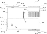
- 1 is a plan view for explaining a laser irradiation apparatus according to a first embodiment;
- FIG. 5 is a cross-sectional view taken along a cutting line VV of the laser irradiation apparatus shown in FIG.
- FIG. 5 is a cross-sectional view taken along a cutting line VI-VI of the laser irradiation apparatus shown in FIG. FIG.
- FIG. 3 is a plan view showing the operation of the laser irradiation apparatus according to the first exemplary embodiment.
- FIG. 3 is a plan view showing the operation of the laser irradiation apparatus according to the first exemplary embodiment.
- FIG. 3 is a plan view showing the operation of the laser irradiation apparatus according to the first exemplary embodiment.
- FIG. 3 is a plan view showing the operation of the laser irradiation apparatus according to the first exemplary embodiment.
- FIG. 3 is a plan view showing the operation of the laser irradiation apparatus according to the first exemplary embodiment.
- FIG. 3 is a plan view showing the operation of the laser irradiation apparatus according to the first exemplary embodiment.
- FIG. 3 is a plan view showing the operation of the laser irradiation apparatus according to the first exemplary embodiment.
- FIG. 6 is a plan view illustrating another configuration example of the laser irradiation apparatus according to the first embodiment.
- FIG. 6 is a plan view illustrating another configuration example of the laser irradiation apparatus according to the first embodiment.
- FIG. 6 is a plan view illustrating another configuration example of the laser irradiation apparatus according to the first embodiment.
- FIG. 6 is a plan view illustrating another configuration example of the laser irradiation apparatus according to the first embodiment.
- FIG. 6 is a plan view illustrating another configuration example of the laser irradiation apparatus according to the first embodiment.
- FIG. 12 is a cross-sectional view taken along a cutting line XII-XII of the laser irradiation apparatus shown in FIG.
- FIG. 6 is a plan view for explaining a laser irradiation apparatus according to a second exemplary embodiment.
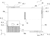
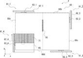
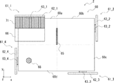
- FIG. 6 is a plan view showing the operation of the laser irradiation apparatus according to the second exemplary embodiment.
- FIG. 6 is a plan view showing the operation of the laser irradiation apparatus according to the second exemplary embodiment.
- FIG. 6 is a plan view showing the operation of the laser irradiation apparatus according to the second exemplary embodiment.
- FIG. 6 is a plan view showing the operation of the laser irradiation apparatus according to the second exemplary embodiment.
- FIG. 6 is a plan view showing the operation of the laser irradiation apparatus according to the second exemplary embodiment.
- FIG. 6 is a plan view showing the operation of the laser irradiation apparatus according to the second exemplary embodiment.
- FIG. 6 is a plan view showing the operation of the laser irradiation apparatus according to the second exemplary embodiment.
- FIG. 6 is a plan view showing the operation of the laser irradiation apparatus according to the second exemplary embodiment.
- FIG. 6 is a plan view showing the operation of the laser irradiation apparatus according to the second exemplary embodiment.
- FIG. 6 is a plan view showing the operation of the laser irradiation apparatus according to the second exemplary embodiment.
- FIG. 6 is a plan view showing the operation of the laser irradiation apparatus according to the second exemplary embodiment.
- FIG. 1 is a plan view for explaining a laser irradiation apparatus according to a comparative example.
- 2 is a cross-sectional view of the laser irradiation apparatus shown in FIG. 1 taken along a cutting line II-II.
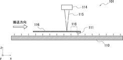
- the laser irradiation apparatus 101 includes a levitation unit 110, a transport unit 111, and a laser light source 114.
- the levitation unit 110 is configured to eject gas from the surface of the levitation unit 110, and the gas ejected from the surface of the levitation unit 110 is blown to the lower surface of the workpiece 116.
- the object to be processed 116 floats.
- the workpiece 116 is a glass substrate.
- the transport unit 111 transports the target object 111 in the transport direction (x-axis direction) while holding the downstream end of the target object 116 in the transport direction.
- the transport unit 111 includes a suction cup type vacuum suction mechanism and a vacuum suction mechanism including a porous body. This vacuum suction mechanism is connected to an exhaust port (not shown), and the exhaust port is connected to an ejector, a vacuum pump, or the like. Therefore, since the negative pressure for sucking the gas acts on the vacuum suction mechanism, the workpiece 116 can be held using the vacuum suction mechanism.
- the transport unit 111 transports the target object 116 in the transport direction using a moving mechanism (not shown) while holding the target object 116.
- the object 116 is irradiated with a laser beam 115 (hereinafter, a laser beam irradiation position is also indicated by reference numeral 115).
- the laser irradiation apparatus is a laser annealing apparatus.
- an excimer laser or the like can be used for the laser generator 114.
- the laser beam supplied from the laser generator 114 becomes a line shape in an optical system (not shown), and a laser beam 115 (line beam) whose line 116, specifically, the focal point extends in the y-axis direction on the object 116 is processed.
- Is irradiated see FIG. 1).
- the object to be processed 116 is an amorphous film formed on a substrate, for example, and the amorphous film is crystallized by irradiating the amorphous film with laser light 115 and annealing. Can do.
- the lower surface of the object to be processed 116 is held using the transport unit 111 while the object to be processed 116 is levitated using the levitating unit 110, and the object to be processed is processed.
- the body 116 is transported in the transport direction.
- the transport unit 111 holds the entire end of the workpiece 116 on the downstream side in the transport direction from the lower surface side of the workpiece 116.
- the stress is transmitted from the transport unit 111 to the object to be processed 116 when the object to be processed 116 is transported, so that the object to be processed 116 is easily bent.
- the conveyance unit 111 is configured to pass the laser irradiation position 115, the workpiece 116 bends in the vicinity of the position where the conveyance unit 111 holds the workpiece 116, and the laser in the workpiece 116.
- unevenness occurs in the irradiation of the laser light because it is out of the depth of focus (DOF) of the light.
- the conveyance unit 111 is configured to pass the laser irradiation position 115, the workpiece 116 bends in a region indicated by reference numeral 118 of the workpiece 116, and the focal depth of the laser light on the workpiece 116 ( There is a problem that unevenness occurs in the irradiation of laser light.
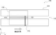
- the transport unit 121 holds the target object 116 along the transport direction of the target object 116 near the center of the target object 116. It occurs in the same way. That is, as in the laser irradiation apparatus 102 illustrated in FIG. 3, stress is easily transmitted from the transfer unit 121 to the target object 116 when the target object 116 is transferred at a position where the transfer unit 121 holds the target object 116. Therefore, the object 116 is easily bent in the thickness direction (z-axis direction) of the object 116 in the vicinity of the region denoted by reference numeral 119 of the object 116.
- the conveyance unit 121 when the conveyance unit 121 is configured to pass the laser irradiation position 115, the workpiece 116 bends in the region indicated by reference numeral 119 of the workpiece 116, and the focal depth of the laser beam on the workpiece 116 ( There is a problem that unevenness occurs in the irradiation of laser light.
- the levitation unit 110 in order to provide the transport unit 121 at the center of the levitation unit 110, the levitation unit 110 is divided at the center to provide a gap 112 through which the transport unit 121 passes. ing.
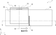
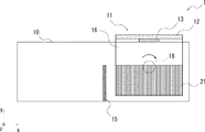
- FIG. 4 is a plan view for explaining the laser irradiation apparatus according to the first embodiment.
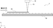
- FIG. 5 is a cross-sectional view of the laser irradiation apparatus shown in FIG. 4 taken along the cutting line VV.
- 6 is a cross-sectional view of the laser irradiation apparatus shown in FIG. 4 taken along section line VI-VI.
- the laser irradiation apparatus 1 includes a floating unit 10, a transport unit 11, and a laser light source 14.
- the levitation unit 10 is configured to eject gas from the surface of the levitation unit 10, and the gas ejected from the surface of the levitation unit 10 is sprayed on the lower surface of the workpiece 16.
- the workpiece 16 is lifted.
- the workpiece 16 is a glass substrate.
- the levitation unit 10 adjusts the flying height so that the workpiece 16 does not come into contact with another mechanism (not shown) disposed above the workpiece 16.
- the transport unit 11 transports the workpiece 16 that is floating in the transport direction (x-axis direction). As shown in FIGS. 4 and 6, the transport unit 11 includes a holding mechanism 12 and a moving mechanism 13.
- the holding mechanism 12 holds the workpiece 16.
- the holding mechanism 12 can be configured using a suction cup type vacuum suction mechanism or a vacuum suction mechanism including a porous body.
- the holding mechanism 12 vacuum adsorption mechanism
- the holding mechanism 12 vacuum adsorption mechanism
- the exhaust port is connected to an ejector, a vacuum pump, or the like. Therefore, since the negative pressure for sucking the gas acts on the holding mechanism 12, the workpiece 16 can be held using the holding mechanism 12.
- the holding mechanism 12 has a surface (upper surface) opposite to the surface (upper surface) irradiated with the laser light of the object 16, that is, the surface of the object 16 to float.
- the workpiece 16 is held by sucking the surface facing the unit 10. Further, the holding mechanism 12 holds the end of the workpiece 16 in the y-axis direction (that is, the end in the direction perpendicular to the transport direction of the workpiece 16).
- the moving mechanism 13 included in the transport unit 11 is connected to the holding mechanism 12.
- the moving mechanism 13 is configured to be able to move the holding mechanism 12 in the transport direction (x-axis direction).
- the transport unit 11 (holding mechanism 12 and moving mechanism 13) is provided on the end side in the y-axis direction of the floating unit 10, and the moving mechanism 13 holds the workpiece 16 with the holding mechanism 12 while the moving mechanism 13 moves in the transport direction.
- the workpiece 16 is transported by moving to.
- the moving mechanism 13 is configured to slide the end of the floating unit 10 in the y-axis direction along the x-axis, and the moving mechanism 13 moves the end of the floating unit 10 to x By sliding along the axis, the workpiece 16 is transported along the x-axis. At this time, the conveyance speed of the workpiece 16 can be controlled by controlling the movement speed of the movement mechanism 13.
- the object 16 is irradiated with a laser beam 15 (hereinafter, the laser beam irradiation position is also indicated by reference numeral 15).
- the laser irradiation apparatus is a laser annealing apparatus.
- an excimer laser or the like can be used for the laser generation apparatus 14.
- the laser light supplied from the laser generator 14 becomes a line shape in an optical system (not shown), and a laser beam 15 (line beam) whose line 16 is formed on the object 16 to be processed, specifically, the focal point extends in the y-axis direction. Is irradiated (see FIG. 4).
- the irradiation position of the laser beam 15 on the workpiece 16 extends in a direction (y-axis direction) perpendicular to the conveyance direction (x-axis direction) of the workpiece 16.
- the object to be processed 16 is an amorphous film formed on a substrate, for example, and the amorphous film is crystallized by irradiating the amorphous film with a laser beam 15 and annealing. Can do.
- the workpiece 16 is held by using the transfer unit 11 while holding the lower surface of the workpiece 16 while the workpiece 16 is levitated using the levitation unit 10. It is transported in the transport direction.
- the transport unit 11 included in the laser irradiation apparatus 1 holds a position where the transport unit 11 does not overlap the laser irradiation position 15 in plan view (that is, when viewed from the z-axis direction) when the workpiece 16 is transported.
- the workpiece 16 is conveyed. That is, as shown in FIG.
- the position where the conveyance unit 11 holds the object 16 is the laser irradiation position 15. I try not to overlap.
- the planar shape of the workpiece 16 is a quadrangle (rectangular shape) having four sides, and the transport unit 11 (holding mechanism 12) holds only one of the four sides of the workpiece 16.
- the transport unit 11 (holding mechanism 12) holds a position where the laser beam is not irradiated during the period in which the workpiece 16 is transported.
- the position where the transport unit 11 holds the workpiece 16 (corresponding to the position of the holding mechanism 12) and the laser irradiation position 15 can be separated. Therefore, the influence of the deflection of the object 16 during laser irradiation can be reduced.
- the target object when stress is transmitted from the transport unit 11 to the target object 16 during transport of the target object 16, the target object is located near the position where the transport unit 11 holds the target object 16 (corresponding to the position of the holding mechanism 12). 16 extends in the thickness direction (z-axis direction). Therefore, when the laser beam 15 is irradiated to this position, there is a problem that the laser beam 15 is deviated from the focal depth (DOF) of the laser beam 16 and the laser beam irradiation is uneven (FIGS. 1 to 5). (See comparative example shown in 3).
- the position where the transport unit 11 holds the workpiece 16 does not overlap the laser irradiation position 15.
- the holding mechanism 12 is configured to hold the end of the workpiece 16 in the y-axis direction.
- the laser irradiation position 15 is arranged so as to be separated from the transport unit 11.
- the laser irradiation position 15 is arranged so as to extend from the y-axis direction negative end of the levitation unit 10 to the vicinity of the center of the levitation unit 10. The length at is about half the length of the floating unit 10 (object 16) in the y-axis direction.
- the position where the transport unit 11 holds the object 16 (corresponding to the position of the holding mechanism 12) and the laser irradiation position 15 can be separated, and the object to be processed at the time of laser irradiation.
- the effect of 16 deflections can be reduced.
- the laser beam 115 is also irradiated on the workpiece 116 just above the transport unit 111, and this also causes unevenness in the irradiation of the laser beam 115.
- the position where the transport unit 11 holds the workpiece 16 does not overlap the laser irradiation position 15. Yes.
- unevenness in laser light irradiation can be suppressed.
- the transport unit 121 is provided in the central portion of the levitation unit 110, the levitation unit 110 is divided at the central portion and the transport unit 121 passes therethrough. It was necessary to provide the gap 112.
- the transport unit 11 is provided at the end of the floating unit 10 in the y-axis direction, it is not necessary to divide the floating unit 10.
- the object 16 can be irradiated with the laser beam 15 by conveying the object 16 in the conveying direction.
- the length of the laser irradiation position 15 in the y-axis direction is about half the length of the workpiece 16 in the y-axis direction.
- the laser irradiation position 15 is arranged on the minus side in the y-axis direction of the levitation unit 10, and when the object 16 passes through the laser irradiation position 15, the laser is applied to a half region in the y-axis direction of the object 16. Light is irradiated.
- the object 16 is reciprocally conveyed to the plus side and the minus side in the x-axis direction, and the object 16 is irradiated with the laser beam 15 in a plurality of times.
- the entire surface of the body 16 can be irradiated with laser light.
- the horizontal surface (xy plane) of the object 16 is held on the downstream side in the conveying direction (x-axis direction) of the levitation unit 10 as shown in FIG. 7A.
- a rotation mechanism 18 that rotates the workpiece 16 by 180 degrees is provided. That is, the laser irradiation apparatus 1 uses the transport unit 11 to transport the object 16 in the transport direction, irradiates the object 16 with the laser light 15, and then uses the rotation mechanism 18 to 180 the object 16 to be processed.
- the entire surface of the target object 16 can be irradiated with the laser beam 15 by rotating the target object 16 in the direction opposite to the transport direction and irradiating the target object 16 with the laser beam 15.
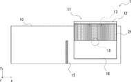
- FIGS. 7A to 7F the operation in this case will be described in detail with reference to FIGS. 7A to 7F.
- the laser beam 15 is irradiated onto the object 16 using the laser irradiation apparatus 1, first, the lower surface of the end of the object 16 in the y-axis direction (facing the levitation unit 10). Side surface) is held using the holding mechanism 12 of the transport unit 11. After that, as shown in FIG. 7B, in the state where the holding mechanism 12 holds the object 16 to be processed, the moving mechanism 13 of the transport unit 11 is moved to the plus side in the x-axis direction, and the object 16 is moved in the x-axis direction plus. To the side. Thereby, the laser beam 15 is irradiated to the half region of the workpiece 16 (the region irradiated with the laser beam is denoted by reference numeral 21).
- the moving mechanism 13 of the transport unit 11 is moved to the minus side in the x-axis direction, and the object to be processed 16 is minus in the x-axis direction. To the side. Thereby, the laser beam 15 is irradiated to the other half region of the workpiece 16. Then, by conveying the object 16 to the position shown in FIG. 7F, the entire surface of the object 16 can be irradiated with laser light.
- the operations shown in FIGS. 7A to 7F may be repeated a plurality of times. As described above, by repeating the operations shown in FIGS. 7A to 7F a plurality of times, the object 16 can pass through the laser irradiation position 15 a plurality of times. The laser beam can be irradiated once.
- the laser irradiation position 15 is arranged so as to extend from the end on the minus side in the y-axis direction of the levitation unit 10 to the vicinity of the center of the levitation unit 10.
- the laser irradiation position 25 may be arranged from the minus side end in the y-axis direction of the levitation unit 10 to the plus side end. Good. By arranging the laser irradiation position 25 in this manner, the area of the laser beam 15 irradiated to the object to be processed 16 can be increased, and the object 16 can be efficiently irradiated with the laser beam 15. .
- the position where the transport unit 11 holds the workpiece 16 (corresponding to the position of the holding mechanism 12) and the laser irradiation position 25 are arranged so as to be separated from each other.
- the laser irradiation position 25 is arranged at a position where there is no influence of the deflection generated in the target object 16 when the transport unit 11 transports the target object 16.
- the transport unit 31 is provided with a plurality of holding mechanisms 32_1 to 32_4, and the end of the object 16 is processed using each holding mechanism 32_1 to 32_4. May be held.
- the four holding mechanisms 32_1 to 32_4 are arranged so as to be separated from each other, and the end of the workpiece 16 is held using these four holding mechanisms 32_1 to 32_4.
- the transport unit 41 is provided with two holding mechanisms 42_1 and 42_2, and the end of the workpiece 16 is held using the holding mechanisms 42_1 and 42_2. May be.
- the two holding mechanisms 42_1 and 42_2 are arranged so as to be separated from each other, the holding mechanism 42_1 is upstream in the transport direction of the object 16 and the holding mechanism 42_2 is downstream in the transport direction of the object 16 Each side is configured to be held.
- the area when the holding mechanisms 42_1 and 42_2 hold the object to be processed 16 in other words, the area where the holding mechanisms 42_1 and 42_2 and the object 16 are in contact can be reduced. Further, it is possible to reduce the influence of the stress acting on the workpiece 16 from the holding mechanisms 42_1 and 42_2.
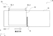
- the holding mechanisms 52_1 and 52_2 of the transport unit 51 are configured to hold both surfaces (upper surface and lower surface) of the object 16 to be processed. May be.
- the two holding mechanisms 52_1 and 52_2 are arranged so as to be separated from each other, the holding mechanism 52_1 is upstream of the workpiece 16 in the transport direction, and the holding mechanism 52_2 is the workpiece 16 of the workpiece 16. It is configured to grip each downstream side in the transport direction.
- the holding mechanisms 52_1 and 52_2 are connected to the moving mechanism 53, and the moving mechanisms 53 move so that the holding mechanisms 52_1 and 52_2 convey the object 16 to be processed.
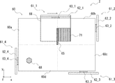
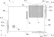
- FIG. 13 is a plan view for explaining the laser irradiation apparatus 2 according to the second embodiment.
- the levitation unit 60 includes four regions 60a to 60d (rectangular regions surrounded by solid lines and broken lines), and the object 66 is processed by these four regions. A case where 60a to 60d are sequentially conveyed and processed will be described. Since the configuration other than this is the same as that of the laser irradiation apparatus 1 described in the first embodiment, redundant description will be omitted as appropriate.
- the laser irradiation apparatus 2 includes a levitation unit 60 and transport units 61_1 to 61_4.
- the levitation unit 60 is configured to eject gas from the surface of the levitation unit 60.
- the gas ejected from the surface of the levitation unit 60 is blown onto the lower surface of the object to be processed 66, so that the object to be processed 66 is Surface.
- the levitation unit 60 includes four areas 60a to 60d.
- the floating unit 60 has a rectangular shape when viewed in plan, and each of the transport units 61_1 to 61_4 transports the object 66 along each side of the floating unit 60.
- the transport unit 61_1 is provided on the side on the plus side in the y-axis direction of the levitation unit 60, and includes a holding mechanism 62_1 and a moving mechanism 63_1. Then, while the workpiece 66 is held by the holding mechanism 62_1, the moving mechanism 63_1 moves to the plus side in the x-axis direction, so that the workpiece 66 can be transported from the region 60a to the region 60b.
- the transport unit 61_2 is provided on the plus side of the levitation unit 60 in the x-axis direction, and includes a holding mechanism 62_2 and a moving mechanism 63_2. Then, the object 66 can be transported from the region 60b to the region 60c by moving the moving mechanism 63_2 to the minus side in the y-axis direction while holding the object 66 by the holding mechanism 62_2.
- the transport unit 61_3 is provided on the negative side of the flying unit 60 in the y-axis direction, and includes a holding mechanism 62_3 and a moving mechanism 63_3. Then, while the workpiece 66 is held by the holding mechanism 62_3, the moving mechanism 63_3 moves to the minus side in the x-axis direction, so that the workpiece 66 can be transported from the region 60c to the region 60d.
- the transport unit 61_4 is provided on the negative side of the levitation unit 60 in the x-axis direction, and includes a holding mechanism 62_4 and a moving mechanism 63_4. Then, while the workpiece 66 is held by the holding mechanism 62_4, the moving mechanism 63_4 moves to the positive side in the y-axis direction, so that the workpiece 66 can be transported from the region 60d to the region 60a.
- the laser irradiation position 65 is provided between the region 60a and the region 60b. Accordingly, the laser beam 65 is irradiated to the object 66 when the object 66 is transported from the region 60a to the region 60b.
- the length of the laser irradiation position 65 in the y-axis direction is about half the length of the workpiece 66 in the y-axis direction. Therefore, when the object to be processed 66 passes through the laser irradiation position 65, the laser beam is irradiated to a half region of the object to be processed 66 in the y-axis direction.
- the target object 60 is conveyed in the order of the regions 60a, 60b, 60c, and 60d, and the target object 66 is irradiated with the laser beam 65 in a plurality of times.
- the entire surface of 66 can be irradiated with laser light.
- the object to be processed is held while the horizontal surface (xy plane) of the object to be processed 66 is held in the region 60d of the levitation unit 60 as shown in FIG.
- a rotation mechanism 68 for rotating 66 by 180 degrees is provided. That is, the object to be processed 66 is transferred from the region 60a to the region 60b using the transfer unit 61_1 and irradiated with the laser beam 65, and then the object to be processed 66 is transferred using the transfer units 61_2 to 61_4. Meanwhile, the object to be processed is rotated 180 degrees using the rotation mechanism 68.
- the object 66 is again conveyed from the region 60a to the region 60b using the conveyance unit 61_1, and the object 66 is irradiated with the laser beam 65, so that the entire surface of the object 66 is irradiated with the laser beam 65. can do.
- these operations will be described in detail with reference to FIGS. 14A to 14J.
- the laser beam 65 is irradiated to the object to be processed 66 using the laser irradiation apparatus 2, first, as shown in FIG. 14A, the lower surface of the end in the y-axis direction of the object to be processed 66 is held by the transport unit 61_1. Holding is performed using the mechanism 62_1. Thereafter, as shown in FIG. 14B, in a state where the holding mechanism 62_1 holds the object to be processed 66, the moving mechanism 63_1 of the transport unit 61_1 is moved to the plus side in the x-axis direction, and the object to be processed 66 is plus in the x-axis direction. To the side. Thereby, the laser beam 65 is irradiated to the half region of the workpiece 66 (the region irradiated with the laser beam is indicated by reference numeral 71).
- the holding mechanism for holding the object 66 is changed from the holding mechanism 62_1 to the holding mechanism 62_2. Further, the transport unit 61_1 is returned to the original position (area 60a).
- the moving mechanism 63_2 of the transport unit 61_2 is moved to the negative side in the y-axis direction so that the object 66 is negative in the y-axis direction. To the side.
- the holding mechanism for holding the object 66 is changed from the holding mechanism 62_2 to the holding mechanism 62_3. Further, the transport unit 61_2 is returned to the original position (area 60b). Thereafter, with the holding mechanism 62_3 holding the workpiece 66, the moving mechanism 63_3 of the transport unit 61_3 is moved to the minus side in the x-axis direction to transport the workpiece 66 to the minus side in the x-axis direction.
- the rotating mechanism 68 is rotated 180 degrees in a state where the workpiece 66 is placed on the rotating mechanism 68.
- the object to be processed 66 rotates 180 degrees, and the region 71 irradiated with the laser light of the object to be processed 66 changes from the y axis direction minus side to the y axis direction plus side, as shown in FIG. 14G.
- the object 66 is held using the holding mechanism 62_4.
- the moving mechanism 63_4 of the transport unit 61_4 is moved to the y-axis direction plus side to transport the workpiece 66 to the y-axis direction plus side.
- the holding mechanism for holding the object 66 is changed from the holding mechanism 62_4 to the holding mechanism 62_1. Further, the transport unit 61_4 is returned to the original position (area 60d).
- the moving mechanism 63_1 of the transport unit 61_1 is moved to the plus side in the x-axis direction, and the object to be processed 66 is plus in the x-axis direction.
- the laser beam 65 is irradiated to the other half region of the object to be processed 66 (the region irradiated with the laser beam is indicated by reference numeral 71).
- the to-be-processed object 66 can be irradiated to the whole surface of the to-be-processed object 66 by conveying the to-be-processed object 66 to the area
- the operations shown in FIGS. 14A to 14J may be repeated a plurality of times. As described above, by repeating the operations shown in FIGS. 14A to 14J a plurality of times, the object to be processed 66 can pass through the laser irradiation position 65 a plurality of times. The laser beam can be irradiated once.
- the location where the rotation mechanism 68 is provided is the region 60c of the levitation unit 60. It may be other than. That is, after passing through the laser irradiation position 65 and before passing through the laser irradiation position 65 again, the object 66 has only to be rotated 180 degrees, and therefore the rotation mechanism 68 is provided at any of the floating units 60a to 60d. If it is.
- the object to be processed 60 is conveyed in the order of the regions 60a, 60b, 60c, and 60d and the object 66 is irradiated with the laser beam 65.
- the object to be processed can be circulated and conveyed.
- the rotation mechanism 68 is preferably provided in a region other than the regions 60a and 60b.
- the rotation mechanism 68 is preferably provided in the region 60d.
- the laser beam 65 is irradiated to the target object 66 when the target object 66 is transferred using the transfer unit 61_1. Therefore, after the transfer unit 61_1 moves to the region 60b, The object to be processed cannot be irradiated with the laser beam 65 until it returns to the region 60a again.
- a transport unit that transports the object to be processed 66 from the region 60a to the region 60b is provided separately from the transport unit 61_1, and the object to be processed 66 is transported alternately using a plurality of transport units. Even during the time until the transport unit 61_1 returns from the region 60b to the region 60a, the workpiece can be irradiated with the laser beam 65 using another transport unit. Therefore, the throughput of the laser irradiation apparatus 2 can be further improved.
- the positions where the transport units 61_1 to 61_4 hold the workpiece 16 do not overlap the laser irradiation position 65. ing.
- the position where the transfer units 61_1 to 61_4 hold the object to be processed 66 and the laser irradiation position 65 can be separated from each other, and the object to be processed 66 is transferred from the transfer units 61_1 to 61_4 when the object 66 is transferred.
- the influence of the deflection of the object to be processed 66 due to the stress being transmitted to the object to be processed 66 that is, the influence of the deflection of the object to be processed 66 during the laser irradiation can be reduced.
- the amorphous film formed over the substrate can be irradiated with laser light to crystallize the amorphous film.
- the semiconductor device is a semiconductor device including a TFT (Thin Film Transistor).
- the amorphous silicon film can be irradiated with laser light to be crystallized to form a polysilicon film.
- FIG. 15 is a cross-sectional view for explaining an example of a semiconductor device manufacturing method.
- the laser irradiation apparatus according to the present embodiment described above is suitable for manufacturing a TFT array substrate.
- a method for manufacturing a semiconductor device having a TFT will be described.
- a gate electrode 202 is formed on a glass substrate 201.
- a metal thin film containing aluminum or the like can be used for the gate electrode 202.
- a gate insulating film 203 is formed on the gate electrode 202.
- the gate insulating film 203 is formed so as to cover the gate electrode 202.
- an amorphous silicon film 204 is formed on the gate insulating film 203 as shown in Step C of FIG.
- the amorphous silicon film 204 is disposed so as to overlap the gate electrode 202 with the gate insulating film 203 interposed therebetween.
- the gate insulating film 203 is a silicon nitride film (SiN x ), a silicon oxide film (SiO 2 film), or a laminated film thereof. Specifically, the gate insulating film 203 and the amorphous silicon film 204 are continuously formed by a CVD (Chemical Vapor Deposition) method.
- CVD Chemical Vapor Deposition
- the amorphous silicon film 204 is crystallized by irradiating the amorphous silicon film 204 with laser light using the laser irradiation apparatus described above to form a polysilicon film 205. .
- a polysilicon film 205 in which silicon is crystallized is formed on the gate insulating film 203.
- the influence of the deflection of the substrate 201 at the time of laser irradiation can be reduced, and the focus of the laser light irradiated on the amorphous silicon film 204 is reduced. It is possible to suppress the deviation from the depth (DOF). Accordingly, a uniformly crystallized polysilicon film 205 can be formed.
- an interlayer insulating film 206, a source electrode 207a, and a drain electrode 207b are formed on the polysilicon film 205.
- the interlayer insulating film 206, the source electrode 207a, and the drain electrode 207b can be formed using a general photolithography method or a film formation method.
- a semiconductor device including a TFT can be manufactured.
- description is abbreviate
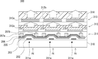
- FIG. 16 is a cross-sectional view for explaining the outline of the organic EL display, and shows a simplified pixel circuit of the organic EL display.
- An organic EL display 300 shown in FIG. 16 is an active matrix display device in which a TFT is disposed in each pixel PX.
- the organic EL display 300 includes a substrate 310, a TFT layer 311, an organic layer 312, a color filter layer 313, and a sealing substrate 314.
- FIG. 16 shows a top emission type organic EL display in which the sealing substrate 314 side is the viewing side.
- the following description shows one configuration example of the organic EL display, and the present embodiment is not limited to the configuration described below.
- the semiconductor device according to the present embodiment may be used in a bottom emission type organic EL display.
- the substrate 310 is a glass substrate or a metal substrate.
- a TFT layer 311 is provided on the substrate 310.
- the TFT layer 311 includes a TFT 311a disposed in each pixel PX. Further, the TFT layer 311 includes a wiring connected to the TFT 311a.
- the TFT 311a, wiring, and the like constitute a pixel circuit. Note that the TFT layer 311 corresponds to the TFT described in FIG. 16, and includes a gate electrode 202, a gate insulating film 203, a polysilicon film 205, an interlayer insulating film 206, a source electrode 207a, and a drain electrode 207b.
- the organic layer 312 has an organic EL light emitting element 312a arranged for each pixel PX.
- the organic EL light emitting element 312a has, for example, a stacked structure in which an anode, a hole injection layer, a hole transport layer, a light emitting layer, an electron transport layer, an electron injection layer, and a cathode are stacked.
- the anode is a metal electrode
- the cathode is a transparent conductive film such as ITO (Indium Tin Oxide).
- the organic layer 312 is provided with a partition 312b for separating the organic EL light emitting element 312a between the pixels PX.
- a color filter layer 313 is provided on the organic layer 312.
- the color filter layer 313 is provided with a color filter 313a for performing color display. That is, each pixel PX is provided with a resin layer colored in R (red), G (green), or B (blue) as the color filter 313a.
- R red
- G green
- B blue
- the color filter layer 313 may be omitted in the case of a three-color system in which the organic layer 312 is provided with organic EL light-emitting elements that emit RGB colors.
- the sealing substrate 314 is a transparent substrate such as a glass substrate, and is provided to prevent deterioration of the organic EL light emitting element of the organic layer 312.
- the current flowing through the organic EL light emitting element 312a of the organic layer 312 varies depending on the display signal supplied to the pixel circuit. Therefore, the amount of light emitted from each pixel PX can be controlled by supplying a display signal corresponding to the display image to each pixel PX. Thereby, a desired image can be displayed.
- an organic EL display has been described as an example of a device using a semiconductor device including a TFT.
- the semiconductor device including a TFT may be a liquid crystal display, for example.
- the laser irradiation apparatus concerning this Embodiment was applied to the laser annealing apparatus was demonstrated above.
- the laser irradiation apparatus according to this embodiment can be applied to apparatuses other than the laser annealing apparatus.
- Laser irradiation device 10 Floating unit 11, 31, 41, 51 Transport unit 12, 32_1 to 32_4, 42_1, 42_2, 52_1, 52_2 Holding mechanism 13, 53 Moving mechanism 14 Laser light source 15, 25, Laser Light, laser irradiation position 16 Object to be processed 18 Rotating mechanism 60 Floating unit 61_1 to 61_4 Transport unit 62_1 to 62_4 Holding mechanism 63_1 to 63_4 Moving mechanism 65 Laser light, laser irradiation position 66 Object to be processed 68 Rotating mechanism
Landscapes
- Physics & Mathematics (AREA)
- Optics & Photonics (AREA)
- Engineering & Computer Science (AREA)
- Plasma & Fusion (AREA)
- Mechanical Engineering (AREA)
- Electromagnetism (AREA)
- Combustion & Propulsion (AREA)
- Chemical & Material Sciences (AREA)
- Laser Beam Processing (AREA)
- Recrystallisation Techniques (AREA)
- Container, Conveyance, Adherence, Positioning, Of Wafer (AREA)
- Bipolar Integrated Circuits (AREA)
- Health & Medical Sciences (AREA)
- Toxicology (AREA)
- Robotics (AREA)
Abstract
一実施の形態にかかるレーザ照射装置(1)は、レーザ光を発生させるレーザ発生装置(14)と、レーザ光が照射される被処理体(16)を浮上させる浮上ユニット(10)と、浮上している被処理体16を搬送する搬送ユニット(11)と、を備える。搬送ユニット(11)は、搬送ユニット(11)がレーザ光の照射位置(15)と重畳しない位置を保持して被処理体(16)を搬送する。一実施の形態にかかるレーザ照射装置(1)により、レーザ光の照射にムラが生じることを抑制することができる。
Description
本発明はレーザ照射装置、レーザ照射方法、及び半導体装置の製造方法に関し、例えば被処理体を搬送する搬送ユニットを備えるレーザ照射装置、レーザ照射方法、及び半導体装置の製造方法に関する。
シリコン基板やガラス基板などに形成された非晶質膜にレーザ光を照射して非晶質膜を結晶化させるレーザアニール装置が知られている。特許文献1には、浮上ユニットを用いて基板を浮上させながら、搬送ユニットを用いて基板を搬送して、基板にレーザ光を照射するレーザアニール装置が開示されている。また、特許文献2には、加工対象物にレーザ光を照射して加工を行うレーザ加工装置が開示されている。
特許文献1に開示されている技術では、浮上ユニットを用いて基板を浮上させながら、搬送ユニットを用いて基板を搬送して、基板にレーザ光を照射している。搬送ユニットを用いて基板を搬送する際は、搬送ユニットを用いて基板を把持するが、この搬送ユニットが基板を把持している位置では、基板の搬送時に搬送ユニットから基板に応力が伝わるため基板がたわみやすい。このため、特許文献1に開示されている技術のように、搬送ユニットがレーザ光の照射位置を通過するような場合は、搬送ユニットが基板を把持している位置付近において基板がたわみ、レーザ光の焦点深度(DOF:Depth of Focus)から外れてしまい、レーザ光の照射にムラが生じるという問題がある。
その他の課題と新規な特徴は、本明細書の記述および添付図面から明らかになるであろう。
一実施の形態にかかるレーザ照射装置は、被処理体を搬送する搬送ユニットを備える。搬送ユニットは、搬送ユニットがレーザ光の照射位置と重畳しない位置を保持して被処理体を搬送する。
前記一実施の形態によれば、レーザ光の照射にムラが生じることを抑制することが可能なレーザ照射装置、レーザ照射方法、及び半導体装置の製造方法を提供することができる。
<レーザ照射装置(比較例)の説明>
まず、比較例にかかるレーザ照射装置について説明する。
図1は、比較例にかかるレーザ照射装置を説明するための平面図である。図2は、図1に示すレーザ照射装置の切断線II-IIにおける断面図である。図1、図2に示すように、レーザ照射装置101は、浮上ユニット110、搬送ユニット111、及びレーザ光源114を備える。
まず、比較例にかかるレーザ照射装置について説明する。
図1は、比較例にかかるレーザ照射装置を説明するための平面図である。図2は、図1に示すレーザ照射装置の切断線II-IIにおける断面図である。図1、図2に示すように、レーザ照射装置101は、浮上ユニット110、搬送ユニット111、及びレーザ光源114を備える。
図2に示すように、浮上ユニット110は、浮上ユニット110の表面からガスを噴出するように構成されており、浮上ユニット110の表面から噴出されたガスが被処理体116の下面に吹き付けられることで、被処理体116が浮上する。例えば、被処理体116はガラス基板である。
搬送ユニット111は、被処理体116の搬送方向下流側の端部を保持して、被処理体111を搬送方向(x軸方向)に搬送する。例えば、搬送ユニット111は、吸盤型の真空吸着機構や多孔質体を備える真空吸着機構を備えている。この真空吸着機構は、排気ポート(不図示)に接続されており、排気ポートはエジェクタや真空ポンプなどに接続されている。よって、真空吸着機構にはガスを吸引するための負圧が作用するため、真空吸着機構を用いて被処理体116を保持することができる。搬送ユニット111は、被処理体116を保持しながら、移動機構(不図示)を用いて被処理体116を搬送方向に搬送する。
被処理体116にはレーザ光115(以下、レーザ光の照射位置も符号115で示す)が照射される。例えば、レーザ照射装置はレーザアニール装置であり、この場合はレーザ発生装置114にエキシマレーザ等を用いることができる。レーザ発生装置114から供給されたレーザ光は、光学系(不図示)においてライン状となり、被処理体116にはライン状、具体的には焦点がy軸方向に伸びるレーザ光115(ラインビーム)が照射される(図1参照)。また、被処理体116は、例えば基板上に形成された非晶質膜であり、この非晶質膜にレーザ光115を照射してアニール処理することで、非晶質膜を結晶化させることができる。
図1、図2に示す比較例にかかるレーザ照射装置では、浮上ユニット110を用いて被処理体116を浮上させながら、搬送ユニット111を用いて被処理体116の下面を保持して、被処理体116を搬送方向に搬送している。このとき、搬送ユニット111は、被処理体116の搬送方向下流側の端部全体を、被処理体116の下面側から保持している。
ここで、搬送ユニット111が被処理体116を保持している位置では、被処理体116の搬送時に搬送ユニット111から被処理体116に応力が伝わるため被処理体116がたわみやすい。このため、搬送ユニット111がレーザ照射位置115を通過するように構成した場合は、搬送ユニット111が被処理体116を保持している位置付近において被処理体116がたわみ、被処理体116におけるレーザ光の焦点深度(DOF:Depth of Focus)から外れてしまい、レーザ光の照射にムラが生じるという問題があった。
具体的には、図1、図2に示すように、搬送ユニット111が被処理体116を保持している位置では、被処理体116の搬送時に搬送ユニット111から被処理体116に応力が伝わりやすく、このため被処理体116の符号118で示す領域付近において、被処理体116が被処理体116の厚さ方向(z軸方向)にたわみやすい。このため、搬送ユニット111がレーザ照射位置115を通過するように構成した場合は、被処理体116の符号118で示す領域において被処理体116がたわみ、被処理体116におけるレーザ光の焦点深度(DOF)から外れてしまい、レーザ光の照射にムラが生じるという問題があった。
このような問題は、図3に示すレーザ照射装置102のように、搬送ユニット121が、被処理体116の中央部付近において被処理体116の搬送方向に沿って被処理体116を保持している場合にも同様に発生する。つまり、図3に示すレーザ照射装置102のように、搬送ユニット121が被処理体116を保持している位置では、被処理体116の搬送時に搬送ユニット121から被処理体116に応力が伝わりやすく、このため被処理体116の符号119で示す領域付近において、被処理体116が被処理体116の厚さ方向(z軸方向)にたわみやすい。このため、搬送ユニット121がレーザ照射位置115を通過するように構成した場合は、被処理体116の符号119で示す領域において被処理体116がたわみ、被処理体116におけるレーザ光の焦点深度(DOF)から外れてしまい、レーザ光の照射にムラが生じるという問題があった。なお、図3に示すレーザ照射装置102では、搬送ユニット121を浮上ユニット110の中央部に設けるために、浮上ユニット110を中央部において分割して、搬送ユニット121が通過するための隙間112を設けている。
以下の実施の形態では、このような問題を解決することが可能なレーザ照射装置、レーザ照射方法、及び半導体装置の製造方法について説明する。
<実施の形態1>
以下、図面を用いて実施の形態1にかかるレーザ照射装置について説明する。図4は、実施の形態1にかかるレーザ照射装置を説明するための平面図である。図5は、図4に示すレーザ照射装置の切断線V-Vにおける断面図である。図6は、図4に示すレーザ照射装置の切断線VI-VIにおける断面図である。
以下、図面を用いて実施の形態1にかかるレーザ照射装置について説明する。図4は、実施の形態1にかかるレーザ照射装置を説明するための平面図である。図5は、図4に示すレーザ照射装置の切断線V-Vにおける断面図である。図6は、図4に示すレーザ照射装置の切断線VI-VIにおける断面図である。
図4~図6に示すように、レーザ照射装置1は、浮上ユニット10、搬送ユニット11、及びレーザ光源14を備える。図5に示すように、浮上ユニット10は、浮上ユニット10の表面からガスを噴出するように構成されており、浮上ユニット10の表面から噴出されたガスが被処理体16の下面に吹き付けられることで、被処理体16が浮上する。例えば、被処理体16はガラス基板である。被処理体16が搬送される際、浮上ユニット10は被処理体16の上側に配置されている他の機構(不図示)に被処理体16が接触しないように浮上量を調整している。
搬送ユニット11は、浮上している被処理体16を搬送方向(x軸方向)に搬送する。図4、図6に示すように、搬送ユニット11は、保持機構12と移動機構13とを備える。保持機構12は、被処理体16を保持する。例えば、保持機構12は、吸盤型の真空吸着機構や多孔質体を備える真空吸着機構を用いて構成することができる。保持機構12(真空吸着機構)は、排気ポート(不図示)に接続されており、排気ポートはエジェクタや真空ポンプなどに接続されている。よって、保持機構12にはガスを吸引するための負圧が作用するため、保持機構12を用いて被処理体16を保持することができる。
本実施の形態では、図6に示すように、保持機構12は、被処理体16のレーザ光が照射される面(上面)と逆側の面(下面)、つまり、被処理体16の浮上ユニット10と対向する側の面を吸引することで、被処理体16を保持している。また、保持機構12は、被処理体16のy軸方向における端部(つまり、被処理体16の搬送方向と垂直な方向における端部)を保持している。
搬送ユニット11が備える移動機構13は保持機構12と連結されている。移動機構13は、保持機構12を搬送方向(x軸方向)に移動可能に構成されている。搬送ユニット11(保持機構12及び移動機構13)は、浮上ユニット10のy軸方向の端部側に設けられており、保持機構12で被処理体16を保持しつつ、移動機構13が搬送方向に移動することで被処理体16が搬送される。
図4に示すように、例えば、移動機構13は浮上ユニット10のy軸方向の端部をx軸に沿ってスライドするように構成されており、移動機構13が浮上ユニット10の端部をx軸に沿ってスライドすることで、被処理体16がx軸に沿って搬送される。このとき、移動機構13の移動速度を制御することで、被処理体16の搬送速度を制御することができる。
図4、図5に示すように、被処理体16にはレーザ光15(以下、レーザ光の照射位置も符号15で示す)が照射される。例えば、レーザ照射装置はレーザアニール装置であり、この場合はレーザ発生装置14にエキシマレーザ等を用いることができる。レーザ発生装置14から供給されたレーザ光は、光学系(不図示)においてライン状となり、被処理体16にはライン状、具体的には焦点がy軸方向に伸びるレーザ光15(ラインビーム)が照射される(図4参照)。換言すると、レーザ光15の被処理体16上における照射位置は被処理体16の搬送方向(x軸方向)と垂直な方向(y軸方向)に伸びている。また、被処理体16は、例えば基板上に形成された非晶質膜であり、この非晶質膜にレーザ光15を照射してアニール処理することで、非晶質膜を結晶化させることができる。
図4~図6に示すレーザ照射装置1では、浮上ユニット10を用いて被処理体16を浮上させながら、搬送ユニット11を用いて被処理体16の下面を保持して、被処理体16を搬送方向に搬送している。このとき、レーザ照射装置1が備える搬送ユニット11は、被処理体16を搬送した際に、平面視において(つまりz軸方向からみて)、搬送ユニット11がレーザ照射位置15と重畳しない位置を保持して被処理体16を搬送している。つまり、図4に示すように、被処理体16を搬送方向に搬送した際に、搬送ユニット11が被処理体16を保持する位置(保持機構12の位置に対応)が、レーザ照射位置15と重畳しないようにしている。
例えば、被処理体16の平面形状は4辺を有する四角形(矩形状)であり、搬送ユニット11(保持機構12)は、被処理体16の4辺中の1辺のみを保持している。そして、搬送ユニット11(保持機構12)は、被処理体16が搬送されている期間においてレーザ光が照射されない位置を保持している。
例えば、被処理体16の平面形状は4辺を有する四角形(矩形状)であり、搬送ユニット11(保持機構12)は、被処理体16の4辺中の1辺のみを保持している。そして、搬送ユニット11(保持機構12)は、被処理体16が搬送されている期間においてレーザ光が照射されない位置を保持している。
このような構成とすることで、搬送ユニット11が被処理体16を保持する位置(保持機構12の位置に対応)とレーザ照射位置15とを離間させることができる。よって、レーザ照射時における被処理体16のたわみの影響を低減させることができる。
つまり、被処理体16の搬送時に搬送ユニット11から被処理体16に応力が伝わると、搬送ユニット11が被処理体16を保持する位置(保持機構12の位置に対応)付近において、被処理体16が厚さ方向(z軸方向)にわたむ。よって、この位置にレーザ光15が照射されると、被処理体16におけるレーザ光の焦点深度(DOF)から外れてしまい、レーザ光の照射にムラが生じるという問題があった(図1~図3に示した比較例参照)。
これに対して本実施の形態では、搬送ユニット11が被処理体16を保持する位置(保持機構12の位置に対応)が、レーザ照射位置15と重畳しないようにしている。具体的には、図4に示すように、保持機構12が、被処理体16のy軸方向における端部を保持するように構成している。また、レーザ照射位置15が搬送ユニット11から離れるように配置している。図4に示す例では、レーザ照射位置15が、浮上ユニット10のy軸方向マイナス側の端部から浮上ユニット10の中央部付近に伸びるように配置しており、レーザ照射位置15のy軸方向における長さは、浮上ユニット10(被処理体16)のy軸方向における長さの半分程度の長さとしている。
このような構成とすることで、搬送ユニット11が被処理体16を保持する位置(保持機構12の位置に対応)とレーザ照射位置15とを離間させることができ、レーザ照射時における被処理体16のたわみの影響を低減させることができる。
よって、レーザ光の照射にムラが生じることを抑制することが可能なレーザ照射装置を提供することができる。
また、図1に示した比較例にかかるレーザ照射装置101では、搬送ユニット111の直上の被処理体116にもレーザ光115が照射されるため、これによってもレーザ光115の照射にムラが生じる場合があった。これに対して本実施の形態では、図4に示すように、搬送ユニット11が被処理体16を保持する位置(保持機構12の位置に対応)が、レーザ照射位置15と重畳しないようにしている。よって、レーザ光の照射にムラが生じることを抑制することができる。
また、図3に示した比較例にかかるレーザ照射装置102では、搬送ユニット121を浮上ユニット110の中央部に設けているため、浮上ユニット110を中央部において分割し、搬送ユニット121が通過するための隙間112を設ける必要があった。これに対して本実施の形態では、図4に示すように、搬送ユニット11を浮上ユニット10のy軸方向の端部に設けているので、浮上ユニット10を分割する必要がない。
次に、本実施の形態にかかるレーザ照射装置1が被処理体16にレーザ光を照射する場合の動作について説明する。図4に示すレーザ照射装置1では、被処理体16を搬送方向に搬送することで被処理体16にレーザ光15を照射することができる。図4に示すレーザ照射装置1では、レーザ照射位置15のy軸方向における長さは、被処理体16のy軸方向における長さの半分程度の長さである。レーザ照射位置15は、浮上ユニット10のy軸方向マイナス側に配置されており、被処理体16がレーザ照射位置15を通過した際に、被処理体16のy軸方向の半分の領域にレーザ光が照射される。
図4に示すレーザ照射装置1では、x軸方向のプラス側とマイナス側に被処理体16を往復搬送し、複数回に分けて被処理体16にレーザ光15を照射することで、被処理体16の全面にレーザ光を照射することができる。
このように被処理体16を往復搬送する場合は、図7Aに示すように、浮上ユニット10の搬送方向(x軸方向)下流側に、被処理体16の水平面(xy平面)を保持しながら被処理体16を180度回転させる回転機構18を設ける。つまり、レーザ照射装置1は、搬送ユニット11を用いて被処理体16を搬送方向に搬送して被処理体16にレーザ光15を照射した後、回転機構18を用いて被処理体16を180度回転させ、被処理体16を搬送方向と逆方向に搬送して被処理体16にレーザ光15を照射することで、被処理体16の全面にレーザ光を照射することができる。以下、この場合の動作について図7A~図7Fを用いて詳細に説明する。
図7Aに示すように、レーザ照射装置1を用いて被処理体16にレーザ光15を照射する場合は、まず、被処理体16のy軸方向の端部の下面(浮上ユニット10と対向する側の面)を、搬送ユニット11の保持機構12を用いて保持する。その後、図7Bに示すように、保持機構12が被処理体16を保持した状態で、搬送ユニット11の移動機構13をx軸方向プラス側に移動させて、被処理体16をx軸方向プラス側に搬送する。これにより、被処理体16の半分の領域にレーザ光15が照射される(レーザ光が照射されている領域を符号21で示す)。
その後、図7Cに示すように、被処理体16がx軸方向プラス側に搬送されて、回転機構18の上に到達した後、保持機構12の保持状態を解放して、保持機構12が被処理体16を保持していない状態とする。そして、回転機構18の上に被処理体16が載っている状態で、回転機構18を180度回転させる。これにより被処理体16が180度回転して、図7Dに示すように、被処理体16のレーザ光が照射された領域21がy軸方向マイナス側からy軸方向プラス側になる。その後、被処理体16のy軸方向の端部の下面を、搬送ユニット11の保持機構12を用いて保持する。
そして、図7Eに示すように、保持機構12が被処理体16を保持した状態で、搬送ユニット11の移動機構13をx軸方向マイナス側に移動させて、被処理体16をx軸方向マイナス側に搬送する。これにより、被処理体16の他方の半分の領域にレーザ光15が照射される。そして、図7Fに示す位置まで被処理体16を搬送することで、被処理体16の全面にレーザ光を照射することができる。
なお、本実施の形態では、図7A~図7Fに示した動作を複数回繰り返すようにしてもよい。このように、図7A~図7Fに示した動作を複数回繰り返すことで、被処理体16がレーザ照射位置15を複数回通過するようにすることができ、被処理体16の同一箇所に複数回レーザ光を照射することができる。
上記で説明したレーザ照射装置1では、図4に示したように、レーザ照射位置15が、浮上ユニット10のy軸方向マイナス側の端部から浮上ユニット10の中央部付近に伸びるように配置し、レーザ照射位置15のy軸方向における長さが浮上ユニット10(被処理体16)のy軸方向における長さの半分程度の長さとした場合について説明した。
しかし本実施の形態では、図8に示すレーザ照射装置1_1のように、浮上ユニット10のy軸方向のマイナス側の端部からプラス側の端部に渡ってレーザ照射位置25を配置してもよい。このようにレーザ照射位置25を配置することで、被処理体16に照射されるレーザ光15の面積を広くすることができ、被処理体16に効率的にレーザ光15を照射することができる。
なお、この場合も、搬送ユニット11が被処理体16を保持する位置(保持機構12の位置に対応)とレーザ照射位置25とが離間するように配置する。換言すると、搬送ユニット11が被処理体16を搬送した際に被処理体16に発生するたわみの影響がない位置に、レーザ照射位置25を配置する。
また、本実施の形態では、図9に示すレーザ照射装置1_2のように、搬送ユニット31に複数の保持機構32_1~32_4を設け、各々の保持機構32_1~32_4を用いて被処理体16の端部を保持するようにしてもよい。図9に示す場合は、4つの保持機構32_1~32_4を互いに離間するように配置し、これら4つの保持機構32_1~32_4を用いて被処理体16の端部を保持している。
このような構成とすることで、保持機構32_1~32_4が被処理体16を保持する際の面積、換言すると、保持機構32_1~32_4と被処理体16とが接触する面積を低減させることができ、保持機構32_1~32_4から被処理体16に働く応力の影響を低減させることができる。
また、図10に示すレーザ照射装置1_3のように、搬送ユニット41に2つの保持機構42_1、42_2を設け、各々の保持機構42_1、42_2を用いて被処理体16の端部を保持するようにしてもよい。図10に示す場合は、2つの保持機構42_1、42_2を互いに離間するように配置し、保持機構42_1が被処理体16の搬送方向上流側を、保持機構42_2が被処理体16の搬送方向下流側をそれぞれ保持するように構成している。
このような構成とすることで、保持機構42_1、42_2が被処理体16を保持する際の面積、換言すると、保持機構42_1、42_2と被処理体16とが接触する面積を低減させることができ、保持機構42_1、42_2から被処理体16に働く応力の影響を低減させることができる。
また、本実施の形態では、図11、図12に示すレーザ照射装置1_4のように、搬送ユニット51の保持機構52_1、52_2が被処理体16の両面(上面および下面)を把持するように構成してもよい。図11、図12に示す例では、2つの保持機構52_1、52_2を互いに離間するように配置し、保持機構52_1が被処理体16の搬送方向上流側を、保持機構52_2が被処理体16の搬送方向下流側をそれぞれ把持するように構成している。図12に示すように、保持機構52_1、52_2は移動機構53と連結されており、移動機構53が移動することで、保持機構52_1、52_2が被処理体16を搬送する。
以上で説明した本実施の形態により、レーザ光の照射にムラが生じることを抑制することが可能なレーザ照射装置およびレーザ照射方法を提供することができる。
<実施の形態2>
次に、実施の形態2について説明する。図13は、実施の形態2にかかるレーザ照射装置2を説明するための平面図である。本実施の形態にかかるレーザ照射装置2では、浮上ユニット60が4つの領域60a~60d(実線と破線で囲まれた矩形状の領域)を備えており、被処理体66がこれらの4つの領域60a~60dを順次搬送されて処理される場合について説明する。これ以外の構成については、実施の形態1で説明したレーザ照射装置1と同様であるので、重複した説明は適宜、省略する。
次に、実施の形態2について説明する。図13は、実施の形態2にかかるレーザ照射装置2を説明するための平面図である。本実施の形態にかかるレーザ照射装置2では、浮上ユニット60が4つの領域60a~60d(実線と破線で囲まれた矩形状の領域)を備えており、被処理体66がこれらの4つの領域60a~60dを順次搬送されて処理される場合について説明する。これ以外の構成については、実施の形態1で説明したレーザ照射装置1と同様であるので、重複した説明は適宜、省略する。
図13に示すように、レーザ照射装置2は、浮上ユニット60および搬送ユニット61_1~61_4を備える。浮上ユニット60は、浮上ユニット60の表面からガスを噴出するように構成されており、浮上ユニット60の表面から噴出されたガスが被処理体66の下面に吹き付けられることで、被処理体66が浮上する。また、浮上ユニット60は4つの領域60a~60dを備える。
図13に示すように、浮上ユニット60は平面視した際の形状が矩形状であり、各々の搬送ユニット61_1~61_4は、浮上ユニット60の各々の辺に沿って被処理体66を搬送するように設けられている。具体的には、搬送ユニット61_1は浮上ユニット60のy軸方向プラス側の辺に設けられており、保持機構62_1と移動機構63_1とを備える。そして、保持機構62_1で被処理体66を保持しつつ、移動機構63_1がx軸方向プラス側に移動することで、被処理体66を領域60aから領域60bに搬送することができる。
搬送ユニット61_2は浮上ユニット60のx軸方向プラス側の辺に設けられており、保持機構62_2と移動機構63_2とを備える。そして、保持機構62_2で被処理体66を保持しつつ、移動機構63_2がy軸方向マイナス側に移動することで、被処理体66を領域60bから領域60cに搬送することができる。
搬送ユニット61_3は浮上ユニット60のy軸方向マイナス側の辺に設けられており、保持機構62_3と移動機構63_3とを備える。そして、保持機構62_3で被処理体66を保持しつつ、移動機構63_3がx軸方向マイナス側に移動することで、被処理体66を領域60cから領域60dに搬送することができる。
搬送ユニット61_4は浮上ユニット60のx軸方向マイナス側の辺に設けられており、保持機構62_4と移動機構63_4とを備える。そして、保持機構62_4で被処理体66を保持しつつ、移動機構63_4がy軸方向プラス側に移動することで、被処理体66を領域60dから領域60aに搬送することができる。
図13に示すレーザ照射装置2では、レーザ照射位置65が領域60aと領域60bとの間に設けられている。よって、被処理体66が領域60aから領域60bに搬送される際にレーザ光65が被処理体66に照射される。
ここで、図13に示すレーザ照射装置2では、レーザ照射位置65のy軸方向における長さは、被処理体66のy軸方向における長さの半分程度の長さである。よって、被処理体66がレーザ照射位置65を通過した際に、被処理体66のy軸方向の半分の領域にレーザ光が照射される。
図13に示すレーザ照射装置2では、被処理体60を領域60a、60b、60c、60dの順に搬送し、複数回に分けて被処理体66にレーザ光65を照射することで、被処理体66の全面にレーザ光を照射することができる。
このように被処理体66の全面にレーザ光を照射する場合は、図13に示すように、浮上ユニット60の領域60dに、被処理体66の水平面(xy平面)を保持しながら被処理体66を180度回転させる回転機構68を設ける。つまり、搬送ユニット61_1を用いて被処理体66を領域60aから領域60bに搬送して被処理体66にレーザ光65を照射した後、搬送ユニット61_2~61_4を用いて被処理体66を搬送させつつ、回転機構68を用いて被処理体を180度回転させる。そして、再度、搬送ユニット61_1を用いて被処理体66を領域60aから領域60bに搬送して被処理体66にレーザ光65を照射することで、被処理体66の全面にレーザ光65を照射することができる。以下、これらの動作について図14A~図14Jを用いて詳細に説明する。
レーザ照射装置2を用いて被処理体66にレーザ光65を照射する場合は、まず、図14Aに示すように、被処理体66のy軸方向の端部の下面を、搬送ユニット61_1の保持機構62_1を用いて保持する。その後、図14Bに示すように、保持機構62_1が被処理体66を保持した状態で、搬送ユニット61_1の移動機構63_1をx軸方向プラス側に移動させて、被処理体66をx軸方向プラス側に搬送する。これにより、被処理体66の半分の領域にレーザ光65が照射される(レーザ光が照射されている領域を符号71で示す)。
図14Cに示すように、被処理体66が浮上ユニット60の領域60bに到達すると、被処理体66を保持する保持機構を保持機構62_1から保持機構62_2に変更する。また、搬送ユニット61_1を元の位置(領域60a)に戻す。
その後、図14Dに示すように、保持機構62_2が被処理体66を保持した状態で、搬送ユニット61_2の移動機構63_2をy軸方向マイナス側に移動させて、被処理体66をy軸方向マイナス側に搬送する。
図14Eに示すように、被処理体66が浮上ユニット60の領域60cに到達すると、被処理体66を保持する保持機構を保持機構62_2から保持機構62_3に変更する。また、搬送ユニット61_2を元の位置(領域60b)に戻す。その後、保持機構62_3が被処理体66を保持した状態で、搬送ユニット61_3の移動機構63_3をx軸方向マイナス側に移動させて、被処理体66をx軸方向マイナス側に搬送する。
そして、図14Fに示すように、被処理体66が浮上ユニット60の領域60dに搬送されて、回転機構68の上に到達した後、保持機構62_3の保持状態を解放して、保持機構62_3が被処理体66を保持していない状態とする。保持機構62_3が被処理体66を解放した後、搬送ユニット61_3は元の位置(領域60d)に戻る。
そして、回転機構68の上に被処理体66が載っている状態で、回転機構68を180度回転させる。これにより被処理体66が180度回転して、図14Gに示すように、被処理体66のレーザ光が照射された領域71がy軸方向マイナス側からy軸方向プラス側になる。その後、被処理体66を保持機構62_4を用いて保持する。そして、保持機構62_4が被処理体66を保持した状態で、搬送ユニット61_4の移動機構63_4をy軸方向プラス側に移動させて、被処理体66をy軸方向プラス側に搬送する。
図14Hに示すように、被処理体66が浮上ユニット60の領域60aに到達すると、被処理体66を保持する保持機構を保持機構62_4から保持機構62_1に変更する。また、搬送ユニット61_4を元の位置(領域60d)に戻す。
その後、図14Iに示すように、保持機構62_1が被処理体66を保持した状態で、搬送ユニット61_1の移動機構63_1をx軸方向プラス側に移動させて、被処理体66をx軸方向プラス側に搬送する。これにより、被処理体66の他方の半分の領域にレーザ光65が照射される(レーザ光が照射されている領域を符号71で示す)。
そして、図14Jに示すように、領域60bまで被処理体66を搬送することで、被処理体66の全面にレーザ光を照射することができる。
なお、本実施の形態では、図14A~図14Jに示した動作を複数回繰り返すようにしてもよい。このように、図14A~図14Jに示した動作を複数回繰り返すことで、被処理体66がレーザ照射位置65を複数回通過するようにすることができ、被処理体66の同一箇所に複数回レーザ光を照射することができる。
なお、上記で説明したレーザ照射装置2では、回転機構68を浮上ユニット60の領域60dに設けた場合につて説明したが、本実施の形態では回転機構68を設ける場所は浮上ユニット60の領域60c以外であってもよい。すなわち、レーザ照射位置65を通過した後、再度レーザ照射位置65を通過する前に被処理体66を180度回転させればよいので、回転機構68を設ける場所は浮上ユニット60a~60dのいずれかであればよい。
また、本実施の形態にかかるレーザ照射装置2では、被処理体60を領域60a、60b、60c、60dの順に搬送して被処理体66にレーザ光65を照射しているので、同時に複数枚の被処理体を循環させて搬送することができる。
つまり、本実施の形態にかかるレーザ照射装置2では、被処理体66にレーザ光65を照射している間に、別の被処理体を搬送したり、回転機構68で回転させたり、被処理体を出し入れしたりすることができる。よって、被処理体66にレーザ光65を照射した後、すぐに他の被処理体にレーザ光65を照射することができるので、レーザ光65が被処理体に照射されない時間を削減することができる。すなわち、本実施の形態では、レーザ照射装置2のスループットを向上させることができる。なお、この場合は、回転機構68を領域60a、60b以外の領域に設けることが好ましく、例えば、回転機構68を領域60dに設けることが好ましい。
また、図13に示した構成では、搬送ユニット61_1を用いて被処理体66を搬送する際に被処理体66にレーザ光65が照射されるので、搬送ユニット61_1が領域60bに移動した後、再び領域60aに戻るまでの間は被処理体にレーザ光65を照射することができない。しかし、例えば、搬送ユニット61_1とは別に、領域60aから領域60bに被処理体66を搬送する搬送ユニットを設け、複数の搬送ユニットを用いて交互に被処理体66を搬送するようにすることで、搬送ユニット61_1が領域60bから領域60aに戻るまでの時間においても別の搬送ユニットを用いて被処理体にレーザ光65を照射することができる。よって、レーザ照射装置2のスループットを更に向上させることができる。
以上で説明したように、本実施の形態においても、搬送ユニット61_1~61_4が被処理体16を保持する位置(保持機構62_1~62_4の位置に対応)が、レーザ照射位置65と重畳しないようにしている。このような構成とすることで、搬送ユニット61_1~61_4が被処理体66を保持する位置とレーザ照射位置65とを離間させることができ、被処理体66の搬送時に搬送ユニット61_1~61_4から被処理体66に応力が伝わることによる被処理体66のたわみの影響、つまり、レーザ照射時における被処理体66のたわみの影響を低減させることができる。
よって、レーザ光の照射にムラが生じることを抑制することが可能なレーザ照射装置を提供することができる。
<その他の実施の形態>
次に、その他の実施の形態として、上記で説明したレーザ照射装置を用いた半導体装置の製造方法について説明する。本実施の形態では、レーザ照射装置としてレーザアニール装置を用いることで、基板上に形成した非晶質膜にレーザ光を照射して非晶質膜を結晶化させることができる。例えば、半導体装置はTFT(Thin Film transistor)を備える半導体装置であり、この場合はアモルファスシリコン膜にレーザ光を照射して結晶化させてポリシリコン膜を形成することができる。
次に、その他の実施の形態として、上記で説明したレーザ照射装置を用いた半導体装置の製造方法について説明する。本実施の形態では、レーザ照射装置としてレーザアニール装置を用いることで、基板上に形成した非晶質膜にレーザ光を照射して非晶質膜を結晶化させることができる。例えば、半導体装置はTFT(Thin Film transistor)を備える半導体装置であり、この場合はアモルファスシリコン膜にレーザ光を照射して結晶化させてポリシリコン膜を形成することができる。
(半導体装置の製造方法)
図15は、半導体装置の製造方法の一例を説明するための断面図である。上記で説明した本実施の形態にかかるレーザ照射装置は、TFTアレイ基板の製造に好適である。以下、TFTを有する半導体装置の製造方法について説明する。
図15は、半導体装置の製造方法の一例を説明するための断面図である。上記で説明した本実施の形態にかかるレーザ照射装置は、TFTアレイ基板の製造に好適である。以下、TFTを有する半導体装置の製造方法について説明する。
まず、図15のステップAに示すように、ガラス基板201上に、ゲート電極202を形成する。ゲート電極202は、例えば、アルミニウムなどを含む金属薄膜を用いることができる。次に、図15のステップBに示すように、ゲート電極202の上に、ゲート絶縁膜203を形成する。ゲート絶縁膜203は、ゲート電極202を覆うように形成される。その後、図15のステップCに示すように、ゲート絶縁膜203の上に、アモルファスシリコン膜204を形成する。アモルファスシリコン膜204は、ゲート絶縁膜203を介して、ゲート電極202と重複するように配置されている。
ゲート絶縁膜203は、窒化シリコン膜(SiNx)、酸化シリコン膜(SiO2膜)、又はこれらの積層膜等などである。具体的には、CVD(Chemical Vapor Deposition)法により、ゲート絶縁膜203とアモルファスシリコン膜204とを連続成膜する。
そして、図15のステップDに示すように、上記で説明したレーザ照射装置を用いてアモルファスシリコン膜204にレーザ光を照射してアモルファスシリコン膜204を結晶化させて、ポリシリコン膜205を形成する。これにより、シリコンが結晶化したポリシリコン膜205がゲート絶縁膜203上に形成される。
このとき、上記で説明した本実施の形態にかかるレーザ照射装置を用いることで、レーザ照射時における基板201のたわみの影響を低減させることができ、アモルファスシリコン膜204に照射されるレーザ光の焦点深度(DOF)から外れてしまうことを抑制することができる。よって、均一に結晶化されたポリシリコン膜205を形成することができる。
その後、図15のステップEに示すように、ポリシリコン膜205の上に層間絶縁膜206、ソース電極207a、及びドレイン電極207bを形成する。層間絶縁膜206、ソース電極207a、及びドレイン電極207bは、一般的なフォトリソグラフィー法や成膜法を用いて形成することができる。
上記で説明した半導体装置の製造方法を用いることで、TFTを備える半導体装置を製造することができる。なお、これ以降の製造工程については、最終的に製造するデバイスによって異なるので説明を省略する。
(有機ELディスプレイ)
次に、TFTを備える半導体装置を用いたデバイスの一例として、有機ELディスプレイについて説明する。図16は、有機ELディスプレイの概要を説明するための断面図であり、有機ELディスプレイの画素回路を簡略化して示している。図16に示す有機ELディスプレイ300は、各画素PXにTFTが配置されたアクティブマトリクス型の表示装置である。
次に、TFTを備える半導体装置を用いたデバイスの一例として、有機ELディスプレイについて説明する。図16は、有機ELディスプレイの概要を説明するための断面図であり、有機ELディスプレイの画素回路を簡略化して示している。図16に示す有機ELディスプレイ300は、各画素PXにTFTが配置されたアクティブマトリクス型の表示装置である。
有機ELディスプレイ300は、基板310、TFT層311、有機層312、カラーフィルタ層313、及び封止基板314を備えている。図16では、封止基板314側が視認側となるトップエミッション方式の有機ELディスプレイを示している。なお、以下の説明は、有機ELディスプレイの一構成例を示すものであり、本実施の形態は、以下に説明される構成に限られるものではない。例えば、本実施の形態にかかる半導体装置は、ボトムエミッション方式の有機ELディスプレイに用いられていてもよい。
基板310は、ガラス基板又は金属基板である。基板310の上には、TFT層311が設けられている。TFT層311は、各画素PXに配置されたTFT311aを有している。さらに、TFT層311は、TFT311aに接続される配線等を有している。TFT311a、及び配線等が画素回路を構成する。なお、TFT層311は、図16で説明したTFTに対応しており、ゲート電極202、ゲート絶縁膜203、ポリシリコン膜205、層間絶縁膜206、ソース電極207a、及びドレイン電極207bを有する。
TFT層311の上には、有機層312が設けられている。有機層312は、画素PXごとに配置された有機EL発光素子312aを有している。有機EL発光素子312aは、例えば、陽極、正孔注入層、正孔輸送層、発光層、電子輸送層、電子注入層、及び陰極が積層された積層構造を有している。トップエミッション方式の場合、陽極は金属電極であり、陰極はITO(Indium Tin Oxide)等の透明導電膜である。さらに、有機層312には、画素PX間において、有機EL発光素子312aを分離するための隔壁312bが設けられている。
有機層312の上には、カラーフィルタ層313が設けられている。カラーフィルタ層313は、カラー表示を行うためのカラーフィルタ313aが設けられている。すなわち、各画素PXには、R(赤色)、G(緑色)、又はB(青色)に着色された樹脂層がカラーフィルタ313aとして設けられている。有機層312から放出された白色光は、カラーフィルタ313aを通過すると、RGBの色の光に変換される。なお、有機層312に、RGBの各色を発光する有機EL発光素子が設けられている3色方式の場合、カラーフィルタ層313を省略してもよい。
カラーフィルタ層313の上には、封止基板314が設けられている。封止基板314は、ガラス基板などの透明基板であり、有機層312の有機EL発光素子の劣化を防ぐために設けられている。
有機層312の有機EL発光素子312aに流れる電流は、画素回路に供給される表示信号によって変化する。よって、表示画像に応じた表示信号を各画素PXに供給することで、各画素PXでの発光量を制御することができる。これにより、所望の画像を表示することができる。
なお、上記では、TFTを備える半導体装置を用いたデバイスの一例として、有機ELディスプレイについて説明したが、TFTを備える半導体装置は、例えば液晶ディスプレイであってもよい。また、上記では、本実施の形態にかかるレーザ照射装置をレーザアニール装置に適用した場合について説明した。しかし、本実施の形態にかかるレーザ照射装置は、レーザアニール装置以外の装置にも適用することができる。
以上、本発明者によってなされた発明を実施の形態に基づき具体的に説明したが、本発明は前記実施の形態に限定されるものではなく、その要旨を逸脱しない範囲で種々変更可能であることはいうまでもない。
この出願は、2016年9月21日に出願された日本出願特願2016-183676を基礎とする優先権を主張し、その開示の全てをここに取り込む。
1、1_1~1_4、2 レーザ照射装置
10 浮上ユニット
11、31、41、51 搬送ユニット
12、32_1~32_4、42_1、42_2、52_1、52_2 保持機構
13、53 移動機構
14 レーザ光源
15、25、 レーザ光、レーザ照射位置
16 被処理体
18 回転機構
60 浮上ユニット
61_1~61_4 搬送ユニット
62_1~62_4 保持機構
63_1~63_4 移動機構
65 レーザ光、レーザ照射位置
66 被処理体
68 回転機構
10 浮上ユニット
11、31、41、51 搬送ユニット
12、32_1~32_4、42_1、42_2、52_1、52_2 保持機構
13、53 移動機構
14 レーザ光源
15、25、 レーザ光、レーザ照射位置
16 被処理体
18 回転機構
60 浮上ユニット
61_1~61_4 搬送ユニット
62_1~62_4 保持機構
63_1~63_4 移動機構
65 レーザ光、レーザ照射位置
66 被処理体
68 回転機構
Claims (28)
- レーザ光を発生させるレーザ発生装置と、
前記レーザ光が照射される被処理体を浮上させる浮上ユニットと、
前記浮上している被処理体を搬送する搬送ユニットと、を備えるレーザ照射装置であって、
前記搬送ユニットは、平面視した際に前記搬送ユニットが前記レーザ光の照射位置と重畳しない位置を保持して前記被処理体を搬送し、
前記浮上ユニットには、前記被処理体の水平面を保持しながら前記被処理体を回転させる回転機構が設けられており、
前記レーザ照射装置は、前記搬送ユニットを用いて前記被処理体を搬送して前記被処理体に前記レーザ光を照射した後、前記回転機構を用いて前記被処理体を回転させ、再度、前記被処理体を搬送して前記被処理体に前記レーザ光を照射する、
レーザ照射装置。 - 前記回転機構は、前記被処理体の水平面を保持しながら前記被処理体を180度回転させるように構成されており、
前記レーザ照射装置は、前記搬送ユニットを用いて前記被処理体を搬送方向に搬送して前記被処理体に前記レーザ光を照射した後、前記回転機構を用いて前記被処理体を180度回転させ、前記被処理体を前記搬送方向と逆方向に搬送して前記被処理体に前記レーザ光を照射する、
請求項1に記載のレーザ照射装置。 - 前記レーザ光は、前記被処理体が搬送された際に前記被処理体の搬送方向と垂直な方向の一部に照射され、
前記搬送ユニットは、前記被処理体の前記搬送方向と垂直な方向における端部を保持して前記被処理体を搬送する、請求項1に記載のレーザ照射装置。 - 前記搬送ユニットは、
前記被処理体を保持する保持機構と、
前記保持機構と連結され、前記浮上ユニットの搬送方向と垂直な方向における端部において前記搬送方向に移動する移動機構と、を備え、
前記保持機構で前記被処理体を保持しつつ、前記移動機構が前記搬送方向に移動することで前記被処理体が搬送される、
請求項1に記載のレーザ照射装置。 - 前記保持機構は、前記被処理体の前記レーザ光が照射される面と逆側の面を吸引することで前記被処理体を保持する、請求項4に記載のレーザ照射装置。
- 前記保持機構は、前記被処理体の両面を把持することで前記被処理体を保持する、請求項4に記載のレーザ照射装置。
- レーザ光を発生させるレーザ発生装置と、
前記レーザ光が照射される被処理体を浮上させる浮上ユニットと、
前記浮上している被処理体を搬送する搬送ユニットと、を備えるレーザ照射装置であって、
前記浮上ユニットは、前記被処理体が搬送される第1乃至第4の領域を備え、
前記搬送ユニットは、
前記被処理体を前記第1の領域から前記第2の領域に搬送する第1の搬送ユニットと、
前記被処理体を前記第2の領域から前記第3の領域に搬送する第2の搬送ユニットと、
前記被処理体を前記第3の領域から前記第4の領域に搬送する第3の搬送ユニットと、
前記被処理体を前記第4の領域から前記第1の領域に搬送する第4の搬送ユニットと、を備え、
前記被処理体が前記第1の領域から前記第2の領域に搬送される際に前記レーザ光が前記被処理体に照射され、
前記第1の搬送ユニットは、平面視した際に前記第1の搬送ユニットが前記レーザ光の照射位置と重畳しない位置を保持して前記被処理体を搬送する、
レーザ照射装置。 - 前記浮上ユニットを平面視した際の形状は矩形状であり、
前記第1の搬送ユニットは前記浮上ユニットの第1の辺に沿って移動することで、前記被処理体を前記第1の領域から前記第2の領域に搬送し、
前記第2の搬送ユニットは前記浮上ユニットの第2の辺に沿って移動することで、前記被処理体を前記第2の領域から前記第3の領域に搬送し、
前記第3の搬送ユニットは前記浮上ユニットの第3の辺に沿って移動することで、前記被処理体を前記第3の領域から前記第4の領域に搬送し、
前記第4の搬送ユニットは前記浮上ユニットの第4の辺に沿って移動することで、前記被処理体を前記第4の領域から前記第1の領域に搬送する、
請求項7に記載のレーザ照射装置。 - 前記レーザ光は、前記被処理体が前記第1の領域から前記第2の領域に搬送された際に前記被処理体の一部に照射され、
前記浮上ユニットの前記第1乃至第4の領域のいずれかには前記被処理体の水平面を保持しながら前記被処理体を180度回転させる回転機構が設けられており、
前記レーザ照射装置は、
前記第1の搬送ユニットを用いて前記被処理体を前記第1の領域から前記第2の領域に搬送して前記被処理体に前記レーザ光を照射し、
前記第2乃至第4の搬送ユニットを用いて前記被処理体を搬送させつつ、前記回転機構を用いて前記被処理体を180度回転させ、
前記第1の搬送ユニットを用いて前記被処理体を前記第1の領域から前記第2の領域に搬送して前記被処理体に前記レーザ光を照射する、
請求項7に記載のレーザ照射装置。 - 前記第1の搬送ユニットは、
前記被処理体を保持する保持機構と、
前記保持機構と連結され、前記浮上ユニットの搬送方向と垂直な方向における端部において前記搬送方向に移動する移動機構と、を備え、
前記保持機構で前記被処理体を保持しつつ、前記移動機構が前記搬送方向に移動することで前記被処理体が搬送される、
請求項7に記載のレーザ照射装置。 - 前記保持機構は、前記被処理体の前記レーザ光が照射される面と逆側の面を吸引することで前記被処理体を保持する、請求項10に記載のレーザ照射装置。
- 前記保持機構は、前記被処理体の両面を把持することで前記被処理体を保持する、請求項11に記載のレーザ照射装置。
- レーザ光を発生させるレーザ発生装置と、
前記レーザ光が照射される被処理体を浮上させる浮上ユニットと、
前記被処理体を搬送する搬送ユニットと、を備えるレーザ照射装置であって、
前記被処理体の平面形状は4辺を有する四角形であり、
前記搬送ユニットは前記被処理体を保持する保持機構を有し、
前記保持機構は、前記被処理体の前記4辺中の1辺のみを保持し、
前記保持機構は、前記被処理体が搬送されている期間において前記レーザ光が照射されない位置にある、
レーザ照射装置。 - 前記保持機構は、前記被処理体の前記レーザ光が照射される面と逆側の面を吸引することで前記被処理体を保持する、請求項13に記載のレーザ照射装置。
- 前記保持機構は、前記被処理体の両面を把持することで前記被処理体を保持する、請求項13に記載のレーザ照射装置。
- 被処理体を浮上ユニットを用いて浮上させながら搬送ユニットを用いて前記被処理体を搬送して前記被処理体にレーザ光を照射するレーザ照射方法であって、
前記搬送ユニットは、平面視した際に前記搬送ユニットが前記レーザ光の照射位置と重畳しない位置を保持して前記被処理体を搬送し、
前記被処理体に前記レーザ光を照射する際、前記搬送ユニットを用いて前記被処理体を搬送して前記被処理体に前記レーザ光を照射した後、前記浮上ユニットに設けられている回転機構を用いて前記被処理体の水平面を保持しながら前記被処理体を回転させ、再度、前記被処理体を搬送して前記被処理体に前記レーザ光を照射する、
レーザ照射方法。 - 前記被処理体に前記レーザ光を照射する際、前記搬送ユニットを用いて前記被処理体を搬送方向に搬送して前記被処理体に前記レーザ光を照射した後、前記浮上ユニットに設けられている回転機構を用いて前記被処理体の水平面を保持しながら前記被処理体を180度回転させ、前記被処理体を前記搬送方向と逆方向に搬送して前記被処理体に前記レーザ光を照射する、請求項16に記載のレーザ照射方法。
- 前記レーザ光は、前記被処理体が搬送された際に前記被処理体の搬送方向と垂直な方向の一部に照射され、
前記搬送ユニットは、前記被処理体の前記搬送方向と垂直な方向における端部を保持して前記被処理体を搬送する、請求項16に記載のレーザ照射方法。 - 前記搬送ユニットが備える保持機構は、前記被処理体の前記レーザ光が照射される面と逆側の面を吸引することで前記被処理体を保持する、請求項16に記載のレーザ照射方法。
- 前記搬送ユニットが備える保持機構は、前記被処理体の両面を把持することで前記被処理体を保持する、請求項16に記載のレーザ照射方法。
- 被処理体を浮上ユニットを用いて浮上させながら第1乃至第4の搬送ユニットを用いて前記被処理体を搬送して前記被処理体にレーザ光を照射するレーザ照射方法であって、
前記第1の搬送ユニットを用いて前記被処理体を第1の領域から第2の領域に搬送し、
前記第2の搬送ユニットを用いて前記被処理体を前記第2の領域から第3の領域に搬送し、
前記第3の搬送ユニットを用いて前記被処理体を前記第3の領域から第4の領域に搬送し、
前記第4の搬送ユニットを用いて前記被処理体を前記第4の領域から前記第1の領域に搬送し、
前記被処理体が前記第1の領域から前記第2の領域に搬送される際に前記レーザ光が前記被処理体に照射され、
前記第1の搬送ユニットは、平面視した際に前記第1の搬送ユニットが前記レーザ光の照射位置と重畳しない位置を保持して前記被処理体を搬送する、
レーザ照射方法。 - 前記浮上ユニットを平面視した際の形状は矩形状であり、
前記第1の搬送ユニットは前記浮上ユニットの第1の辺に沿って移動することで、前記被処理体を前記第1の領域から前記第2の領域に搬送し、
前記第2の搬送ユニットは前記浮上ユニットの第2の辺に沿って移動することで、前記被処理体を前記第2の領域から前記第3の領域に搬送し、
前記第3の搬送ユニットは前記浮上ユニットの第3の辺に沿って移動することで、前記被処理体を前記第3の領域から前記第4の領域に搬送し、
前記第4の搬送ユニットは前記浮上ユニットの第4の辺に沿って移動することで、前記被処理体を前記第4の領域から前記第1の領域に搬送する、
請求項21に記載のレーザ照射方法。 - 被処理体を浮上ユニットを用いて浮上させながら搬送ユニットを用いて前記被処理体を搬送して前記被処理体にレーザ光を照射するレーザ照射方法であって、
前記被処理体の平面形状は4辺を有する四角形であり、
前記搬送ユニットは前記被処理体を保持する保持機構を有し、
前記保持機構は、前記被処理体の前記4辺中の1辺のみを保持するとともに、前記被処理体が搬送されている期間において前記被処理体の前記レーザ光が照射されない位置を保持する、
レーザ照射方法。 - 前記保持機構は、前記被処理体の前記レーザ光が照射される面と逆側の面を吸引することで前記被処理体を保持する、請求項23に記載のレーザ照射方法。
- 前記保持機構は、前記被処理体の両面を把持することで前記被処理体を保持する、請求項23に記載のレーザ照射方法。
- (a)基板上に非晶質膜を形成するステップと、
(b)前記非晶質膜にレーザ光を照射して前記非晶質膜を結晶化させるステップと、を含む半導体装置の製造方法であって、
前記(b)のステップは、前記基板を浮上ユニットを用いて浮上させながら搬送ユニットを用いて前記基板を搬送して前記非晶質膜にレーザ光を照射するステップであり、
前記搬送ユニットは、平面視した際に前記搬送ユニットが前記レーザ光の照射位置と重畳しない位置を保持して前記基板を搬送し、
前記基板に前記レーザ光を照射する際、前記搬送ユニットを用いて前記基板を搬送して前記基板に前記レーザ光を照射した後、前記浮上ユニットに設けられている回転機構を用いて前記基板の水平面を保持しながら前記基板を回転させ、再度、前記基板を搬送して前記基板に前記レーザ光を照射する、
半導体装置の製造方法。 - (a)基板上に非晶質膜を形成するステップと、
(b)前記非晶質膜にレーザ光を照射して前記非晶質膜を結晶化させるステップと、を含む半導体装置の製造方法であって、
前記(b)のステップは、前記基板を浮上ユニットを用いて浮上させながら第1乃至第4の搬送ユニットを用いて前記基板を搬送して前記非晶質膜にレーザ光を照射するステップであり、
前記第1の搬送ユニットを用いて前記基板を第1の領域から第2の領域に搬送し、
前記第2の搬送ユニットを用いて前記基板を前記第2の領域から第3の領域に搬送し、
前記第3の搬送ユニットを用いて前記基板を前記第3の領域から第4の領域に搬送し、
前記第4の搬送ユニットを用いて前記基板を前記第4の領域から前記第1の領域に搬送し、
前記基板を前記第1の領域から前記第2の領域に搬送した際に前記レーザ光を前記基板に照射し、
前記第1の搬送ユニットは、平面視した際に前記第1の搬送ユニットが前記レーザ光の照射位置と重畳しない位置を保持して前記基板を搬送する、
半導体装置の製造方法。 - (a)基板上に非晶質膜を形成するステップと、
(b)前記非晶質膜にレーザ光を照射して前記非晶質膜を結晶化させるステップと、を含む半導体装置の製造方法であって、
前記(b)のステップは、前記基板を浮上ユニットを用いて浮上させながら搬送ユニットを用いて前記基板を搬送して前記非晶質膜にレーザ光を照射するステップであり、
前記基板の平面形状は4辺を有する四角形であり、
前記搬送ユニットは前記基板を保持する保持機構を有し、
前記保持機構は、前記基板の前記4辺中の1辺のみを保持するとともに、前記基板が搬送されている期間において前記基板の前記レーザ光が照射されない位置を保持する、
半導体装置の製造方法。
Priority Applications (4)
| Application Number | Priority Date | Filing Date | Title |
|---|---|---|---|
| KR1020197009593A KR20190051007A (ko) | 2016-09-21 | 2017-06-02 | 레이저 조사 장치, 레이저 조사 방법, 및 반도체 장치의 제조 방법 |
| CN201780055165.0A CN109690739B (zh) | 2016-09-21 | 2017-06-02 | 激光照射装置、激光照射方法以及半导体器件制造方法 |
| US16/327,842 US11355343B2 (en) | 2016-09-21 | 2017-06-02 | Laser irradiation apparatus, laser irradiation method, and method of manufacturing semiconductor device |
| SG11201901520QA SG11201901520QA (en) | 2016-09-21 | 2017-06-02 | Laser irradiation apparatus, laser irradiation method, and method of manufacturing semiconductor device |
Applications Claiming Priority (2)
| Application Number | Priority Date | Filing Date | Title |
|---|---|---|---|
| JP2016-183676 | 2016-09-21 | ||
| JP2016183676A JP6887234B2 (ja) | 2016-09-21 | 2016-09-21 | レーザ照射装置、レーザ照射方法、及び半導体装置の製造方法 |
Publications (1)
| Publication Number | Publication Date |
|---|---|
| WO2018055840A1 true WO2018055840A1 (ja) | 2018-03-29 |
Family
ID=61690311
Family Applications (1)
| Application Number | Title | Priority Date | Filing Date |
|---|---|---|---|
| PCT/JP2017/020641 Ceased WO2018055840A1 (ja) | 2016-09-21 | 2017-06-02 | レーザ照射装置、レーザ照射方法、及び半導体装置の製造方法 |
Country Status (7)
| Country | Link |
|---|---|
| US (1) | US11355343B2 (ja) |
| JP (1) | JP6887234B2 (ja) |
| KR (1) | KR20190051007A (ja) |
| CN (1) | CN109690739B (ja) |
| SG (1) | SG11201901520QA (ja) |
| TW (1) | TW201814811A (ja) |
| WO (1) | WO2018055840A1 (ja) |
Cited By (2)
| Publication number | Priority date | Publication date | Assignee | Title |
|---|---|---|---|---|
| WO2019138659A1 (ja) * | 2018-01-11 | 2019-07-18 | 株式会社日本製鋼所 | レーザ処理装置、レーザ処理方法及び半導体装置の製造方法 |
| WO2024214213A1 (ja) * | 2023-04-12 | 2024-10-17 | Jswアクティナシステム株式会社 | 搬送装置、レーザ照射装置、搬送方法、及び半導体装置の製造方法 |
Families Citing this family (4)
| Publication number | Priority date | Publication date | Assignee | Title |
|---|---|---|---|---|
| KR102702310B1 (ko) | 2019-04-29 | 2024-09-04 | 삼성전자주식회사 | 마이크로 led 전사 방법 및 이에 의해 제조된 디스플레이 모듈 |
| KR102725001B1 (ko) * | 2022-06-08 | 2024-11-01 | 에이피시스템 주식회사 | 레이저 처리장치 |
| JPWO2024009470A1 (ja) * | 2022-07-07 | 2024-01-11 | ||
| JP2024116774A (ja) * | 2023-02-16 | 2024-08-28 | Jswアクティナシステム株式会社 | 搬送装置、レーザ照射装置、搬送方法、及び有機elディスプレイ装置の製造方法 |
Citations (6)
| Publication number | Priority date | Publication date | Assignee | Title |
|---|---|---|---|---|
| JP2004179653A (ja) * | 2002-11-15 | 2004-06-24 | Semiconductor Energy Lab Co Ltd | 半導体膜の作製方法及び半導体装置の作製方法、並びにレーザー処理装置 |
| JP2006505953A (ja) * | 2002-11-06 | 2006-02-16 | ウルトラテック インク | レーザ走査装置および熱処理方法 |
| JP2009010161A (ja) * | 2007-06-28 | 2009-01-15 | Sumitomo Heavy Ind Ltd | レーザ加工装置、及び、レーザ加工方法 |
| JP2012503311A (ja) * | 2008-09-17 | 2012-02-02 | アプライド マテリアルズ インコーポレイテッド | 基板のアニールにおける熱量の管理 |
| JP2012182273A (ja) * | 2011-03-01 | 2012-09-20 | Hitachi High-Technologies Corp | ガラス基板インライン検査方法及びその装置 |
| WO2013069056A1 (ja) * | 2011-11-09 | 2013-05-16 | パナソニック株式会社 | 薄膜形成基板及び薄膜形成方法 |
Family Cites Families (16)
| Publication number | Priority date | Publication date | Assignee | Title |
|---|---|---|---|---|
| JPH02161721A (ja) * | 1988-12-14 | 1990-06-21 | Sony Corp | 光cvd装置 |
| JP3054310B2 (ja) * | 1994-03-09 | 2000-06-19 | 株式会社半導体エネルギー研究所 | 半導体デバイスのレーザー処理方法 |
| JP4974416B2 (ja) | 2001-01-30 | 2012-07-11 | 株式会社半導体エネルギー研究所 | レーザアニール装置 |
| US7232715B2 (en) | 2002-11-15 | 2007-06-19 | Semiconductor Energy Laboratory Co., Ltd. | Method for fabricating semiconductor film and semiconductor device and laser processing apparatus |
| JP4116465B2 (ja) * | 2003-02-20 | 2008-07-09 | 株式会社日立製作所 | パネル型表示装置とその製造方法および製造装置 |
| JP2006135251A (ja) * | 2004-11-09 | 2006-05-25 | Hitachi Ltd | レーザ結晶化装置 |
| TW200741883A (en) * | 2006-04-21 | 2007-11-01 | Zeiss Carl Laser Optics Gmbh | Apparatus for laser annealing of large substrates and method for laser annealing for large substrates |
| US8314369B2 (en) | 2008-09-17 | 2012-11-20 | Applied Materials, Inc. | Managing thermal budget in annealing of substrates |
| JP5843292B2 (ja) * | 2013-03-21 | 2016-01-13 | 株式会社日本製鋼所 | アニール処理半導体基板の製造方法、走査装置およびレーザ処理装置 |
| JP6560198B2 (ja) * | 2014-05-12 | 2019-08-14 | 株式会社日本製鋼所 | レーザアニール装置、レーザアニール処理用連続搬送路およびレーザアニール処理方法 |
| JP6854605B2 (ja) * | 2016-08-29 | 2021-04-07 | 株式会社日本製鋼所 | レーザ照射装置、レーザ照射方法、及び半導体装置の製造方法 |
| JP6764305B2 (ja) * | 2016-10-04 | 2020-09-30 | 株式会社日本製鋼所 | レーザ照射装置、半導体装置の製造方法、及び、レーザ照射装置の動作方法 |
| JP6829118B2 (ja) * | 2017-03-16 | 2021-02-10 | 株式会社日本製鋼所 | レーザ照射装置、レーザ照射方法、及び半導体装置の製造方法 |
| JP6983578B2 (ja) * | 2017-08-25 | 2021-12-17 | 株式会社日本製鋼所 | レーザ照射装置、レーザ照射方法、及び半導体装置の製造方法 |
| JP7083645B2 (ja) * | 2018-01-11 | 2022-06-13 | Jswアクティナシステム株式会社 | レーザ処理装置、レーザ処理方法及び半導体装置の製造方法 |
| JP2021019036A (ja) * | 2019-07-18 | 2021-02-15 | 株式会社日本製鋼所 | レーザ照射装置、レーザ照射方法、及び半導体装置の製造方法 |
-
2016
- 2016-09-21 JP JP2016183676A patent/JP6887234B2/ja active Active
-
2017
- 2017-06-02 KR KR1020197009593A patent/KR20190051007A/ko not_active Withdrawn
- 2017-06-02 US US16/327,842 patent/US11355343B2/en active Active
- 2017-06-02 WO PCT/JP2017/020641 patent/WO2018055840A1/ja not_active Ceased
- 2017-06-02 CN CN201780055165.0A patent/CN109690739B/zh active Active
- 2017-06-02 SG SG11201901520QA patent/SG11201901520QA/en unknown
- 2017-09-01 TW TW106129992A patent/TW201814811A/zh unknown
Patent Citations (6)
| Publication number | Priority date | Publication date | Assignee | Title |
|---|---|---|---|---|
| JP2006505953A (ja) * | 2002-11-06 | 2006-02-16 | ウルトラテック インク | レーザ走査装置および熱処理方法 |
| JP2004179653A (ja) * | 2002-11-15 | 2004-06-24 | Semiconductor Energy Lab Co Ltd | 半導体膜の作製方法及び半導体装置の作製方法、並びにレーザー処理装置 |
| JP2009010161A (ja) * | 2007-06-28 | 2009-01-15 | Sumitomo Heavy Ind Ltd | レーザ加工装置、及び、レーザ加工方法 |
| JP2012503311A (ja) * | 2008-09-17 | 2012-02-02 | アプライド マテリアルズ インコーポレイテッド | 基板のアニールにおける熱量の管理 |
| JP2012182273A (ja) * | 2011-03-01 | 2012-09-20 | Hitachi High-Technologies Corp | ガラス基板インライン検査方法及びその装置 |
| WO2013069056A1 (ja) * | 2011-11-09 | 2013-05-16 | パナソニック株式会社 | 薄膜形成基板及び薄膜形成方法 |
Cited By (3)
| Publication number | Priority date | Publication date | Assignee | Title |
|---|---|---|---|---|
| WO2019138659A1 (ja) * | 2018-01-11 | 2019-07-18 | 株式会社日本製鋼所 | レーザ処理装置、レーザ処理方法及び半導体装置の製造方法 |
| US12011777B2 (en) | 2018-01-11 | 2024-06-18 | Jsw Aktina System Co., Ltd | Laser processing apparatus, laser processing method, and method for manufacturing semiconductor device |
| WO2024214213A1 (ja) * | 2023-04-12 | 2024-10-17 | Jswアクティナシステム株式会社 | 搬送装置、レーザ照射装置、搬送方法、及び半導体装置の製造方法 |
Also Published As
| Publication number | Publication date |
|---|---|
| SG11201901520QA (en) | 2019-03-28 |
| KR20190051007A (ko) | 2019-05-14 |
| TW201814811A (zh) | 2018-04-16 |
| CN109690739A (zh) | 2019-04-26 |
| US11355343B2 (en) | 2022-06-07 |
| JP6887234B2 (ja) | 2021-06-16 |
| JP2018049897A (ja) | 2018-03-29 |
| CN109690739B (zh) | 2023-11-10 |
| US20190198326A1 (en) | 2019-06-27 |
Similar Documents
| Publication | Publication Date | Title |
|---|---|---|
| WO2018055840A1 (ja) | レーザ照射装置、レーザ照射方法、及び半導体装置の製造方法 | |
| JP6854605B2 (ja) | レーザ照射装置、レーザ照射方法、及び半導体装置の製造方法 | |
| US12138710B2 (en) | Laser processing apparatus and method of manufacturing semiconductor device | |
| US11676831B2 (en) | Laser irradiation apparatus, laser irradiation method, and method for manufacturing semiconductor device | |
| JP6764305B2 (ja) | レーザ照射装置、半導体装置の製造方法、及び、レーザ照射装置の動作方法 | |
| CN111066123B (zh) | 激光照射装置、激光照射方法以及半导体器件制造方法 | |
| JP2018064048A (ja) | レーザ照射装置、レーザ照射方法、及び半導体装置の製造方法 | |
| JP7763792B2 (ja) | 搬送装置、搬送方法、及び半導体装置の製造方法 | |
| KR20160049382A (ko) | 레이저 박리 장치 및 표시 장치의 제조 방법 | |
| JP7083645B2 (ja) | レーザ処理装置、レーザ処理方法及び半導体装置の製造方法 | |
| JP6917691B2 (ja) | レーザ照射装置、レーザ照射方法、及び半導体装置の製造方法 | |
| WO2018179201A1 (ja) | 吸着装置、運搬装置、elデバイス製造装置 | |
| JP7412111B2 (ja) | レーザ処理装置及び半導体装置の製造方法 | |
| JP6775449B2 (ja) | レーザ照射装置、レーザ照射方法、及び半導体装置の製造方法 | |
| JP2021077904A (ja) | レーザ照射装置 |
Legal Events
| Date | Code | Title | Description |
|---|---|---|---|
| 121 | Ep: the epo has been informed by wipo that ep was designated in this application |
Ref document number: 17852621 Country of ref document: EP Kind code of ref document: A1 |
|
| NENP | Non-entry into the national phase |
Ref country code: DE |
|
| ENP | Entry into the national phase |
Ref document number: 20197009593 Country of ref document: KR Kind code of ref document: A |
|
| 122 | Ep: pct application non-entry in european phase |
Ref document number: 17852621 Country of ref document: EP Kind code of ref document: A1 |