WO2018047407A1 - バスバーの接続方法、プリント基板、及びスイッチ装置 - Google Patents
バスバーの接続方法、プリント基板、及びスイッチ装置 Download PDFInfo
- Publication number
- WO2018047407A1 WO2018047407A1 PCT/JP2017/017625 JP2017017625W WO2018047407A1 WO 2018047407 A1 WO2018047407 A1 WO 2018047407A1 JP 2017017625 W JP2017017625 W JP 2017017625W WO 2018047407 A1 WO2018047407 A1 WO 2018047407A1
- Authority
- WO
- WIPO (PCT)
- Prior art keywords
- circuit board
- printed circuit
- bus bar
- semiconductor switch
- switch element
- Prior art date
- Legal status (The legal status is an assumption and is not a legal conclusion. Google has not performed a legal analysis and makes no representation as to the accuracy of the status listed.)
- Ceased
Links
Images


Classifications
-
- H—ELECTRICITY
- H01—ELECTRIC ELEMENTS
- H01R—ELECTRICALLY-CONDUCTIVE CONNECTIONS; STRUCTURAL ASSOCIATIONS OF A PLURALITY OF MUTUALLY-INSULATED ELECTRICAL CONNECTING ELEMENTS; COUPLING DEVICES; CURRENT COLLECTORS
- H01R12/00—Structural associations of a plurality of mutually-insulated electrical connecting elements, specially adapted for printed circuits, e.g. printed circuit boards [PCB], flat or ribbon cables, or like generally planar structures, e.g. terminal strips, terminal blocks; Coupling devices specially adapted for printed circuits, flat or ribbon cables, or like generally planar structures; Terminals specially adapted for contact with, or insertion into, printed circuits, flat or ribbon cables, or like generally planar structures
- H01R12/50—Fixed connections
- H01R12/51—Fixed connections for rigid printed circuits or like structures
- H01R12/55—Fixed connections for rigid printed circuits or like structures characterised by the terminals
- H01R12/58—Fixed connections for rigid printed circuits or like structures characterised by the terminals terminals for insertion into holes
-
- H—ELECTRICITY
- H03—ELECTRONIC CIRCUITRY
- H03K—PULSE TECHNIQUE
- H03K17/00—Electronic switching or gating, i.e. not by contact-making and –breaking
- H03K17/51—Electronic switching or gating, i.e. not by contact-making and –breaking characterised by the components used
- H03K17/56—Electronic switching or gating, i.e. not by contact-making and –breaking characterised by the components used by the use, as active elements, of semiconductor devices
- H03K17/687—Electronic switching or gating, i.e. not by contact-making and –breaking characterised by the components used by the use, as active elements, of semiconductor devices the devices being field-effect transistors
- H03K17/6871—Electronic switching or gating, i.e. not by contact-making and –breaking characterised by the components used by the use, as active elements, of semiconductor devices the devices being field-effect transistors the output circuit comprising more than one controlled field-effect transistor
- H03K17/6874—Electronic switching or gating, i.e. not by contact-making and –breaking characterised by the components used by the use, as active elements, of semiconductor devices the devices being field-effect transistors the output circuit comprising more than one controlled field-effect transistor in a symmetrical configuration
-
- H—ELECTRICITY
- H05—ELECTRIC TECHNIQUES NOT OTHERWISE PROVIDED FOR
- H05K—PRINTED CIRCUITS; CASINGS OR CONSTRUCTIONAL DETAILS OF ELECTRIC APPARATUS; MANUFACTURE OF ASSEMBLAGES OF ELECTRICAL COMPONENTS
- H05K1/00—Printed circuits
- H05K1/02—Details
-
- H—ELECTRICITY
- H05—ELECTRIC TECHNIQUES NOT OTHERWISE PROVIDED FOR
- H05K—PRINTED CIRCUITS; CASINGS OR CONSTRUCTIONAL DETAILS OF ELECTRIC APPARATUS; MANUFACTURE OF ASSEMBLAGES OF ELECTRICAL COMPONENTS
- H05K1/00—Printed circuits
- H05K1/18—Printed circuits structurally associated with non-printed electric components
- H05K1/181—Printed circuits structurally associated with non-printed electric components associated with surface mounted components
-
- H—ELECTRICITY
- H05—ELECTRIC TECHNIQUES NOT OTHERWISE PROVIDED FOR
- H05K—PRINTED CIRCUITS; CASINGS OR CONSTRUCTIONAL DETAILS OF ELECTRIC APPARATUS; MANUFACTURE OF ASSEMBLAGES OF ELECTRICAL COMPONENTS
- H05K3/00—Apparatus or processes for manufacturing printed circuits
- H05K3/30—Assembling printed circuits with electric components, e.g. with resistors
- H05K3/32—Assembling printed circuits with electric components, e.g. with resistors electrically connecting electric components or wires to printed circuits
- H05K3/34—Assembling printed circuits with electric components, e.g. with resistors electrically connecting electric components or wires to printed circuits by soldering
- H05K3/3405—Edge mounted components, e.g. terminals
-
- B—PERFORMING OPERATIONS; TRANSPORTING
- B60—VEHICLES IN GENERAL
- B60R—VEHICLES, VEHICLE FITTINGS, OR VEHICLE PARTS, NOT OTHERWISE PROVIDED FOR
- B60R16/00—Electric or fluid circuits specially adapted for vehicles and not otherwise provided for; Arrangement of elements of electric or fluid circuits specially adapted for vehicles and not otherwise provided for
- B60R16/02—Electric or fluid circuits specially adapted for vehicles and not otherwise provided for; Arrangement of elements of electric or fluid circuits specially adapted for vehicles and not otherwise provided for electric constitutive elements
- B60R16/03—Electric or fluid circuits specially adapted for vehicles and not otherwise provided for; Arrangement of elements of electric or fluid circuits specially adapted for vehicles and not otherwise provided for electric constitutive elements for supply of electrical power to vehicle subsystems or for
-
- H—ELECTRICITY
- H01—ELECTRIC ELEMENTS
- H01R—ELECTRICALLY-CONDUCTIVE CONNECTIONS; STRUCTURAL ASSOCIATIONS OF A PLURALITY OF MUTUALLY-INSULATED ELECTRICAL CONNECTING ELEMENTS; COUPLING DEVICES; CURRENT COLLECTORS
- H01R12/00—Structural associations of a plurality of mutually-insulated electrical connecting elements, specially adapted for printed circuits, e.g. printed circuit boards [PCB], flat or ribbon cables, or like generally planar structures, e.g. terminal strips, terminal blocks; Coupling devices specially adapted for printed circuits, flat or ribbon cables, or like generally planar structures; Terminals specially adapted for contact with, or insertion into, printed circuits, flat or ribbon cables, or like generally planar structures
- H01R12/50—Fixed connections
- H01R12/51—Fixed connections for rigid printed circuits or like structures
- H01R12/53—Fixed connections for rigid printed circuits or like structures connecting to cables except for flat or ribbon cables
-
- H—ELECTRICITY
- H03—ELECTRONIC CIRCUITRY
- H03K—PULSE TECHNIQUE
- H03K2217/00—Indexing scheme related to electronic switching or gating, i.e. not by contact-making or -breaking covered by H03K17/00
- H03K2217/0009—AC switches, i.e. delivering AC power to a load
-
- H—ELECTRICITY
- H05—ELECTRIC TECHNIQUES NOT OTHERWISE PROVIDED FOR
- H05K—PRINTED CIRCUITS; CASINGS OR CONSTRUCTIONAL DETAILS OF ELECTRIC APPARATUS; MANUFACTURE OF ASSEMBLAGES OF ELECTRICAL COMPONENTS
- H05K1/00—Printed circuits
- H05K1/02—Details
- H05K1/0213—Electrical arrangements not otherwise provided for
- H05K1/0263—High current adaptations, e.g. printed high current conductors or using auxiliary non-printed means; Fine and coarse circuit patterns on one circuit board
-
- H—ELECTRICITY
- H05—ELECTRIC TECHNIQUES NOT OTHERWISE PROVIDED FOR
- H05K—PRINTED CIRCUITS; CASINGS OR CONSTRUCTIONAL DETAILS OF ELECTRIC APPARATUS; MANUFACTURE OF ASSEMBLAGES OF ELECTRICAL COMPONENTS
- H05K2201/00—Indexing scheme relating to printed circuits covered by H05K1/00
- H05K2201/10—Details of components or other objects attached to or integrated in a printed circuit board
- H05K2201/10007—Types of components
- H05K2201/10166—Transistor
-
- H—ELECTRICITY
- H05—ELECTRIC TECHNIQUES NOT OTHERWISE PROVIDED FOR
- H05K—PRINTED CIRCUITS; CASINGS OR CONSTRUCTIONAL DETAILS OF ELECTRIC APPARATUS; MANUFACTURE OF ASSEMBLAGES OF ELECTRICAL COMPONENTS
- H05K2201/00—Indexing scheme relating to printed circuits covered by H05K1/00
- H05K2201/10—Details of components or other objects attached to or integrated in a printed circuit board
- H05K2201/10227—Other objects, e.g. metallic pieces
- H05K2201/10272—Busbars, i.e. thick metal bars mounted on the printed circuit board [PCB] as high-current conductors
-
- H—ELECTRICITY
- H05—ELECTRIC TECHNIQUES NOT OTHERWISE PROVIDED FOR
- H05K—PRINTED CIRCUITS; CASINGS OR CONSTRUCTIONAL DETAILS OF ELECTRIC APPARATUS; MANUFACTURE OF ASSEMBLAGES OF ELECTRICAL COMPONENTS
- H05K2201/00—Indexing scheme relating to printed circuits covered by H05K1/00
- H05K2201/10—Details of components or other objects attached to or integrated in a printed circuit board
- H05K2201/10227—Other objects, e.g. metallic pieces
- H05K2201/10409—Screws
-
- H—ELECTRICITY
- H05—ELECTRIC TECHNIQUES NOT OTHERWISE PROVIDED FOR
- H05K—PRINTED CIRCUITS; CASINGS OR CONSTRUCTIONAL DETAILS OF ELECTRIC APPARATUS; MANUFACTURE OF ASSEMBLAGES OF ELECTRICAL COMPONENTS
- H05K2201/00—Indexing scheme relating to printed circuits covered by H05K1/00
- H05K2201/10—Details of components or other objects attached to or integrated in a printed circuit board
- H05K2201/10431—Details of mounted components
- H05K2201/10507—Involving several components
- H05K2201/10522—Adjacent components
Definitions
- the present invention relates to a method for connecting a bus bar to a printed circuit board, a printed circuit board to which the bus bar is connected, and a switch device using the printed circuit board to which the bus bar is connected.
- an auxiliary battery (usually a lead storage battery) is mounted on a vehicle, and the auxiliary battery supplies power to a starter motor and various electrical components (see, for example, Patent Document 1).
- a mechanical relay is generally used as a switch for turning on / off the auxiliary battery.
- semiconductor switches for example, MOSFETs (Metal-Oxide-Semiconductor-Field-Effect-Transistors) that have less noise than mechanical relays.
- Semiconductor switches must be mounted on a circuit board and used. In general, a circuit board equipped with a semiconductor switch is connected to the auxiliary battery and the power supply line with a bus bar, so that it can withstand a large current.
- the bus bar is connected to the circuit board by soldering. Stresses such as vibration, impact, and distortion during assembly are applied to the soldering location. Especially in in-vehicle applications, large vibrations and impacts frequently occur. If excessive stress is continuously applied to the soldered part for a long period of time, solder cracks are likely to occur, and eventually there may be a disconnection.
- the present invention has been made in view of such circumstances, and an object thereof is to provide a technique for firmly connecting a bus bar to a circuit board.
- a printed circuit board is a printed circuit board to which a bus bar is connected, the bus bar is soldered to a wiring pattern, and the bus bar is screwed to the printed circuit board. Has been.
- the bus bar can be firmly connected to the circuit board.
- FIG. 1 is a schematic cross-sectional view of a printed circuit board according to an embodiment of the present invention.
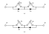
- 4A and 4B are diagrams showing a circuit configuration of the bidirectional switch device. It is a figure for demonstrating the vehicle power supply system using the bidirectional
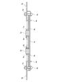
- FIG. 1 is a plan view schematically showing the surface of a printed circuit board 1 according to an embodiment of the present invention.
- a first semiconductor switch element 2a and a second semiconductor switch element 2b are mounted on the surface of the printed circuit board 1 according to the present embodiment.
- the first semiconductor switch element 2a and the second semiconductor switch element 2b are arranged side by side in the longitudinal direction of the printed circuit board 1, and constitute a series circuit. Since a parasitic diode is formed between the source and the drain of the MOSFET, the current flowing from the source terminal cannot be cut off even when the MOSFET is off. When it is desired to cut off bidirectional current, it is common to configure a bidirectional switch by connecting two MOSFETs in series in opposite directions.
- the first bus bar 3a and the second bus bar 3b are connected to both ends in the longitudinal direction of the printed circuit board 1, respectively.
- the first bus bar 3 a and the second bus bar 3 b are each soldered to the wiring pattern of the printed circuit board 1 and screwed to the printed circuit board 1.
- the first soldering portion 6a of the printed circuit board 1 is formed with two holes into which bent portions formed on the left and right of the front end portion of the first bus bar 3a are inserted.
- the bent portions formed on the left and right of the front end portion of the first bus bar 3a are bent at a right angle with respect to the main body portion of the first bus bar 3a, and are formed in the two holes of the first soldering portion 6a of the printed circuit board 1. Installed.
- FIG. 2 is a plan view schematically showing the back surface of the printed circuit board 1 according to the embodiment of the present invention.
- the two bent portions of the first bus bar 3a attached to the two holes of the first soldering portion 6a of the printed circuit board 1 are fixed to the two holes by soldering.
- tip of two bending parts has protruded the back surface.
- the first bolt 4a is passed through the screw hole of the first bus bar 3a and the first screw hole of the printed circuit board 1, and the first bolt 4a.
- the tip of is fastened with the first nut 5a.
- the two holes of the first soldering portion 6a of the printed circuit board 1 and the first screw holes are formed at positions corresponding to the positions of the two bent portions of the first bus bar 3a and the screw holes of the first bus bar 3a.
- the first bolt 4 a is inserted from the back surface of the printed circuit board 1, and is fixed by the first nut 5 a on the front surface of the printed circuit board 1.
- the first bolt 4a may be inserted from the front surface of the printed circuit board 1 and fixed by the first nut 5a on the back surface of the printed circuit board 1.
- the first bolt 4a may be fixed to the first screw hole of the printed circuit board 1 by soldering instead of the first nut 5a. Further, the contact strength may be increased by further soldering from above the first nut 5a.
- the second soldering portion 6b of the printed circuit board 1 is formed with two holes into which the bent portions formed on the left and right of the front end portion of the second bus bar 3b are inserted.
- the two bent portions of the second bus bar 3b are fixed to the two holes of the second soldering portion 6b of the printed circuit board 1 by soldering.
- the second bolt 4b is passed through the screw hole of the second bus bar 3b and the second screw hole of the printed circuit board 1, and the tip of the second bolt 4b is fastened by the second nut 5b.
- the first bolt 4a and the second bolt 4b are made of a conductive material such as copper.
- FIG. 3 is a schematic cross-sectional view of the printed circuit board 1 according to the embodiment of the present invention.
- a wiring pattern is formed on the printed circuit board 1.
- the wiring pattern is formed of a conductive material such as copper foil.
- the first soldering portion 6a and the first drain terminal 7a of the first semiconductor switch element 2a are electrically connected via the first conductive layer 9a.
- the first conductive layer 9a extends to the first screw hole of the printed circuit board 1 and is electrically connected to the first bolt 4a. Copper plating may be applied to the inner wall surface of the first screw hole. Insulating layers are formed above and below the first conductive layer 9a.
- the front and back surfaces of the printed board 1 are covered with a protective film.
- the second soldering portion 6b and the second drain terminal 7b of the second semiconductor switch element 2b are electrically connected via the second conductive layer 9b.
- the second conductive layer 9b extends to the second screw hole of the printed circuit board 1 and is electrically connected to the second bolt 4b. Copper plating may also be applied to the inner wall surface of the second screw hole. Insulating layers are formed above and below the second conductive layer 9b.
- the first source terminal 8a of the first semiconductor switch element 2a and the second source terminal 8b of the second semiconductor switch element 2b are electrically connected via the third conductive layer 9c. Insulating layers are formed above and below the third conductive layer 9c.
- the first conductive layer 9a, the second conductive layer 9b, and the third conductive layer 9c are separated from each other by an insulating wall and are electrically separated.
- the printed circuit board 1 has a wiring pattern for supplying power to the first semiconductor switch element 2a and the second semiconductor switch element 2b, and a drive signal to the gate terminals of the first semiconductor switch element 2a and the second semiconductor switch element 2b. A wiring pattern for supply is also formed, but is omitted in FIGS.
- FIG. 4A shows a circuit configuration of the first semiconductor switch element 2a and the second semiconductor switch element 2b mounted on the printed circuit board 1 shown in FIGS.
- the drain terminal of the first semiconductor switch element 2a is connected to the first bus bar 3a
- the drain terminal of the second semiconductor switch element 2b is connected to the second bus bar 3b
- the source terminal of the first semiconductor switch element 2a and the second semiconductor switch The source terminal of the element 2b is connected.
- a first parasitic diode Da is formed between the source and drain of the first semiconductor switch element 2a
- a second parasitic diode Db is formed between the source and drain of the second semiconductor switch element 2b
- the first parasitic diode Da The anode and the anode of the second parasitic diode Db face each other.
- a high level drive signal (ON signal) is input to the gate terminals of the first semiconductor switch element 2a and the second semiconductor switch element 2b.
- a low-level drive signal (OFF signal) is input to the gate terminals of the first semiconductor switch element 2a and the second semiconductor switch element 2b. Since the anodes of the first parasitic diode Da and the second parasitic diode Db face each other, the current passing through the first parasitic diode Da and the second parasitic diode Db does not flow in either direction.
- FIG. 4B shows a circuit configuration in which the directions of the first semiconductor switch element 2a and the second semiconductor switch element 2b in FIG. 4A are reversed.
- the source terminal of the first semiconductor switch element 2a is connected to the first bus bar 3a
- the source terminal of the second semiconductor switch element 2b is connected to the second bus bar 3b
- the drain terminal of the first semiconductor switch element 2a and the second semiconductor switch The drain terminal of the element 2b is connected.
- a first parasitic diode Da is formed between the source and drain of the first semiconductor switch element 2a
- a second parasitic diode Db is formed between the source and drain of the second semiconductor switch element 2b
- the cathode of the first parasitic diode Da The cathodes of the second parasitic diode Db are facing each other. Therefore, when the first semiconductor switch element 2a and the second semiconductor switch element 2b are in the OFF state, the current passing through the first parasitic diode Da and the second parasitic diode Db does not flow in either direction.
- the present embodiment it is possible to improve the connection strength between the bus bar and the printed board by soldering the bus bar to the printed board and screwing it.
- the bus bar and the printed circuit board are fixed only by soldering, the mechanical strength is insufficient and a countermeasure against stress is required.
- a countermeasure against stress it is conceivable to use a flexible bus bar or to make the bus bar itself a harness.
- the former increases the cost greatly, and the latter has a too large harness diameter.
- the current carrying area can be increased by bringing the conductive bolts used for screwing into contact with the wiring pattern. Therefore, a larger current can be passed. Further, when the current value does not change, the resistance value decreases, so that heat generation can be suppressed. Thermal stress on the solder can also be reduced, improving reliability.
- the positions of the screw holes of the first bus bar 3a / second bus bar 3b and the first screw holes / second screw holes of the printed circuit board 1 are prevented from shifting. be able to.
- the screw holes of the first bus bar 3a / second bus bar 3b and the positions of the first screw holes / second screw holes of the printed circuit board 1 may be slightly shifted. Further, when soldering is performed first, there may be a gap between the first bus bar 3a / second bus bar 3b and the printed circuit board 1.
- the first bus bar 3a / second bus bar 3b When the first bus bar 3a / second bus bar 3b is screwed to the printed circuit board 1 with a part of the first bus bar 3a / second bus bar 3b floating with respect to the printed circuit board 1, the first bus bar 3a / second bus bar The first bus bar 3a / second bus bar 3b is deformed so that 3b is pressed against the printed circuit board 1. In this state, a stress corresponding to the displacement of the first bus bar 3a / second bus bar 3b is applied to the soldered portion.
- the screwing is performed first and the soldering is performed later, the formation of a gap between the first bus bar 3a / second bus bar 3b and the printed circuit board 1 can be suppressed, and the soldering portion Can be prevented from being stressed.
- the above-described bidirectional switch device is suitable for in-vehicle use because it is resistant to vibration, impact, and high temperature environment and can switch a large current.
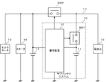
- FIG. 5 is a diagram for explaining a vehicle power supply system using the bidirectional switch device according to the embodiment of the present invention.
- the vehicle power supply system includes a lead storage battery 13 and a sub battery system 10 that reinforces the lead storage battery 13.
- a starter 14, an alternator 15, and an electrical component 16 are mounted as members related thereto.
- the starter 14 is a motor for starting the engine.
- the starter 14 is rotated by the electric power supplied from the lead storage battery 13 and starts the engine.
- an ignition switch (not shown) is turned on by the driver's operation, electric power is supplied from the lead storage battery 13 to the starter 14 via the feeder line L1, and the starter 14 is started.
- the alternator 15 generates electricity by the rotational energy of the crankshaft of the engine.
- the alternator 15 supplies the generated power to the lead storage battery 13 and / or the sub-battery system 10 via the feeder line L1.
- the electrical component 16 is a generic name indicating various electric loads (auxiliaries) mounted in a vehicle such as a headlight, a power steering, an oil pump, a car navigation system, and an audio.
- the starter 14 and the alternator 15 are drawn separately from the electrical component 16.
- the electrical component 16 is driven by electric power supplied from the lead storage battery 13 and / or the sub battery system 10 via the feeder line L1.
- the lead storage battery 13 is a main battery for storing the power generated by the alternator 15 and supplying power to the starter 14 and the electrical component 16.
- the sub-battery system 10 includes a nickel metal hydride storage battery 11, a management device 12, and a first switch device SW1.
- the nickel metal hydride storage battery 11 is a sub-battery for storing the electric power generated by the alternator 15 and supplying power to the electrical component 16.
- the capacity of the nickel hydride storage battery 11 is designed to be smaller than the capacity of the lead storage battery 13.
- the lead storage battery 13 and the nickel metal hydride storage battery 11 are connected in parallel.
- the lead storage battery 13 is relatively inexpensive, can operate in a relatively wide temperature range, has advantages such as high output, and is widely used as a storage battery for vehicles. However, there are disadvantages such as low charge / discharge energy efficiency, weakness against overdischarge, and short cycle life.
- the nickel metal hydride storage battery 11 has advantages such as relatively high charge / discharge energy efficiency, strong overcharge and overdischarge, a wide use temperature range, a wide SOC (State (Of Charge) range, and a relatively long cycle life. .
- a lithium ion storage battery may be used instead of the nickel metal hydride storage battery 11.
- a lithium ion storage battery is a high-performance storage battery with high energy density and charge / discharge energy efficiency. However, strict voltage / temperature management is required. Further, instead of the nickel metal hydride storage battery 11, a capacitor such as an electric double layer capacitor or a lithium ion capacitor may be used.
- the first switch device SW1 is inserted between the positive electrode of the nickel metal hydride storage battery 11 and the power supply line L1.
- the second switch device SW2 is inserted between the connection point of the lead storage battery 13 and the connection point of the nickel metal hydride storage battery 11 of the power supply line L1.
- the bidirectional switch device according to the above embodiment is used for the first switch device SW1 and / or the second switch device SW2.
- the first bus bar 3a fixed to the printed circuit board 1 is connected to the power supply line L1
- the second bus bar 3b fixed to the printed circuit board 1 is described as the positive electrode of the nickel metal hydride storage battery 11. .
- the first bus bar 3a fixed to the printed circuit board 1 is connected to the connection point on the nickel metal hydride storage battery 11 side of the power supply line L1, and the second bus bar 3b fixed to the printed circuit board 1 is connected. It connects with the connection point by the side of the lead storage battery 13 of the feeder L1.
- the management device 12 monitors the voltage, current, and temperature of the nickel metal hydride storage battery 11, manages the state of the nickel metal hydride storage battery 11, and controls charging and discharging of the nickel metal hydride storage battery 11. Specifically, based on the voltage, current, and temperature, SOC (State Of Charge) management and SOH (State Of Health) management of the nickel metal hydride storage battery 11 are performed. Moreover, if the management apparatus 12 detects an overvoltage, an undervoltage, an overcurrent, or temperature abnormality, it will turn off 1st switch apparatus SW1 and will stop charging / discharging. When it is desired to electrically disconnect the lead storage battery 13 and the nickel metal hydride storage battery 11, the management device 12 turns off the second switch device SW2 and disconnects them.
- a mechanical relay Since a bidirectional current flows through the first switch device SW1 and the second switch device SW2, a mechanical relay is generally used. However, since mechanical relays have physical contacts, noise is generated during switching. Therefore, noise during switching can be suppressed by using the bidirectional switch device including the first semiconductor switch element 2a and the second semiconductor switch element 2b described above. In addition, the bidirectional switch device has a strong connection to the bus bar and the printed circuit board, and is resistant to vibration and impact. Therefore, even if the mechanical relay is replaced with a semiconductor switch, reliability equivalent to that of the mechanical relay can be ensured.
- a plurality of series circuits of the first semiconductor switch element 2a and the second semiconductor switch element 2b may be arranged in parallel on the printed circuit board 1 to increase the current capacity of the semiconductor switch.
- the printed circuit board 1 is composed of a multilayer substrate, and a first soldering portion in which the first drain terminal 7a of the first semiconductor switch element 2a and the bent portion of the first bus bar 3a are mounted with a plurality of insulated conductive layers. 6a may be made conductive. Similarly, other conductive portions may be made conductive by a plurality of conductive layers. In this case, the energization area increases and the current capacity increases.
- the printed circuit board 1 on which the bidirectional switch in which the first semiconductor switch element 2a and the second semiconductor switch element 2b are connected in series is mounted has been described.
- the present technology can also be applied to the printed circuit board 1 on which a unidirectional switch composed of one semiconductor switch element is mounted.
- the first bus bar 3a is connected to the drain terminal of the semiconductor switch element
- the second bus bar 3b is connected to the source terminal.
- MOSFET Insulated Gate Bipolar Transistors
- the electronic component mounted on the printed circuit board 1 to which the first bus bar 3a and / or the second bus bar 3b is connected is not limited to a semiconductor switch element.
- the present technology can also be applied to the printed circuit board 1 on which other electronic components such as an amplifier are mounted.
- [Item 1] A method of connecting the bus bars (3a, 3b) for connecting the bus bars (3a, 3b) to the wiring pattern of the printed circuit board (1), Screwing the bus bars (3a, 3b) to the printed circuit board (1); Soldering the bus bars (3a, 3b) to the wiring pattern of the printed circuit board (1) after the bus bars (3a, 3b) are screwed to the printed circuit board (1);
- a bus bar (3a, 3b) connection method characterized by comprising: According to this, the connection between the bus bars (3a, 3b) and the printed circuit board (1) can be strengthened. Further, it is possible to prevent the positional deviation between the screw holes of the bus bars (3a, 3b) and the screw holes of the printed circuit board (1), which may occur when soldering first.
- the printed circuit board (1) characterized by the above-mentioned. According to this, the connection between the bus bars (3a, 3b) and the printed circuit board (1) can be strengthened.
- the bolts (4a, 4b) passing through the holes of the bus bars (3a, 3b) and the holes of the printed circuit board (1) are fastened with nuts (5a, 5b); Item 3.
- a switch device characterized by that. According to this, it is possible to construct a bidirectional switch device in which the connection between the bus bars (3a, 3b) and the printed circuit board (1) is strong.
- the first bus bar (3a) is connected to a power supply line (L1) for supplying power to loads (14, 16) in the vehicle,
- the switch device according to item 5 wherein the second bus bar (3b) is connected to a power storage device (11) mounted in the vehicle. According to this, it can utilize for a vehicle-mounted power supply system.
Landscapes
- Engineering & Computer Science (AREA)
- Microelectronics & Electronic Packaging (AREA)
- Manufacturing & Machinery (AREA)
- Structure Of Printed Boards (AREA)
- Connection Or Junction Boxes (AREA)
- Manufacturing Of Printed Wiring (AREA)
- Structures For Mounting Electric Components On Printed Circuit Boards (AREA)
- Mechanical Engineering (AREA)
Abstract
バスバーを回路基板に強固に接続するために、バスバー(3a/3b)が接続されたプリント基板(1)において、配線パターンにバスバーが半田付けされており、かつ当該バスバー(3a/3b)が当該プリント基板(1)にネジ止めされている。バスバー(3a/3b)の孔とプリント基板(1)の孔を貫通したボルト(4a/4b)の先端部が、ナット(5a/5b)で締結されていてもよい。プリント基板(1)の孔は、当該配線パターンと導通していてもよい。
Description
本発明は、プリント基板へのバスバーの接続方法、バスバーが接続されたプリント基板、及びバスバーが接続されたプリント基板を使用したスイッチ装置に関する。
現在、車両には補機バッテリ(通常、鉛蓄電池)が搭載されており、補機バッテリは、スタータモータや各種の電装品に電力を供給する(例えば、特許文献1参照)。補機バッテリをオン/オフするためのスイッチには、メカリレーを使用することが一般的である。近年、メカリレーと比較して騒音が小さい半導体スイッチ(例えば、MOSFET(Metal-Oxide-Semiconductor Field-Effect Transistor)を使用することが試みられている。半導体スイッチは、回路基板に実装して使用する必要がある。半導体スイッチを搭載した回路基板は補機バッテリと給電線にそれぞれバスバーで接続し、大電流に耐えうる堅牢な設計にすることが一般的である。
通常、バスバーは回路基板に半田付けで接続される。半田付け箇所には振動、衝撃、組み付け時の歪み等のストレスが加わる。特に車載用途では、大きな振動や衝撃が頻繁に発生する。過大なストレスが半田付け箇所に長期間継続的に加わると、半田クラックが発生しやすくなり、最終的に断線に至るケースもある。
本発明はこうした状況に鑑みなされたものであり、その目的は、バスバーを回路基板に強固に接続する技術を提供することにある。
上記課題を解決するために、本発明のある態様のプリント基板は、バスバーが接続されたプリント基板であって、配線パターンにバスバーが半田付けされており、かつ当該バスバーが当該プリント基板にネジ止めされている。
なお、以上の構成要素の任意の組み合わせ、本発明の表現を方法、装置、システムなどの間で変換したものもまた、本発明の態様として有効である。
本発明によれば、バスバーを回路基板に強固に接続することができる。
図1は、本発明の実施の形態に係るプリント基板1の表面の概略を示す平面図である。本実施の形態に係るプリント基板1の表面には、第1半導体スイッチ素子2a及び第2半導体スイッチ素子2bが実装される。以下、半導体スイッチ素子としてMOSFETを使用する例を説明する。第1半導体スイッチ素子2a及び第2半導体スイッチ素子2bは、プリント基板1の長手方向に並べて配置され、直列回路を構成する。MOSFETはソース-ドレイン間に寄生ダイオードが形成されるため、MOSFETがオフ状態でもソース端子から流入する電流を遮断することができない。双方向の電流を遮断したい場合、2つのMOSFETを逆向きに直列接続して、双方向スイッチを構成することが一般的である。
プリント基板1の長手方向の両端に、第1バスバー3a及び第2バスバー3bがそれぞれ接続される。第1バスバー3a及び第2バスバー3bはそれぞれプリント基板1の配線パターンに半田付けされるとともに、プリント基板1にネジ止めされる。プリント基板1の第1半田付け部6aには、第1バスバー3aの先端部の左右に形成された折曲部が挿入される、2つの孔が形成されている。第1バスバー3aの先端部の左右に形成された折曲部は、第1バスバー3aの本体部に対して直角に折り曲げられており、プリント基板1の第1半田付け部6aの2つの孔に装着される。
図2は、本発明の実施の形態に係るプリント基板1の裏面の概略を示す平面図である。プリント基板1の第1半田付け部6aの2つの孔に装着された、第1バスバー3aの2つの折曲部は、半田付けにより当該2つの孔に固定される。なお図2に示すように2つの折曲部の先端は、裏面をはみ出している。
第1バスバー3aの折曲部が第1半田付け部6aに固定された後、第1バスバー3aのネジ孔とプリント基板1の第1ネジ孔に第1ボルト4aが貫通され、第1ボルト4aの先端が第1ナット5aで締結される。プリント基板1の第1半田付け部6aの2つの孔、及び第1ネジ孔は、第1バスバー3aの2つの折曲部、及び第1バスバー3aのネジ孔の位置に対応した位置に形成される。図1、図2に示す例では、プリント基板1の裏面から第1ボルト4aが挿入され、プリント基板1の表面で第1ナット5aにより固定される。なお反対に、プリント基板1の表面から第1ボルト4aが挿入され、プリント基板1の裏面で第1ナット5aにより固定されてもよい。
なお第1ナット5aの代わりに半田付けにより、第1ボルト4aをプリント基板1の第1ネジ孔に固定してもよい。また第1ナット5aの上からさらに半田付けをして、接触強度を高めてもよい。
同様にプリント基板1の第2半田付け部6bには、第2バスバー3bの先端部の左右に形成された折曲部が挿入される、2つの孔が形成される。第2バスバー3bの2つの折曲部は、プリント基板1の第2半田付け部6bの2つの孔に半田付けにより固定される。その後、第2バスバー3bのネジ孔とプリント基板1の第2ネジ孔に第2ボルト4bが貫通され、第2ボルト4bの先端が第2ナット5bで締結される。第1ボルト4a及び第2ボルト4bには、銅などの導電材で生成されたものを使用する。
図3は、本発明の実施の形態に係るプリント基板1の概略断面図である。プリント基板1には、配線パターンが形成されている。配線パターンは、銅箔などの導電材で形成される。第1半田付け部6aと第1半導体スイッチ素子2aの第1ドレイン端子7aは、第1導電層9aを経由して導通している。第1導電層9aはプリント基板1の第1ネジ孔まで延びており、第1ボルト4aと導通している。第1ネジ孔の内壁面には、銅めっきが施されてもよい。第1導電層9aの上下には絶縁層が形成されている。プリント基板1の表面および裏面は保護皮膜により覆われている。
同様に、第2半田付け部6bと第2半導体スイッチ素子2bの第2ドレイン端子7bは、第2導電層9bを経由して導通している。第2導電層9bはプリント基板1の第2ネジ孔まで延びており、第2ボルト4bと導通している。第2ネジ孔の内壁面にも、銅めっきが施されてもよい。第2導電層9bの上下には絶縁層が形成されている。
第1半導体スイッチ素子2aの第1ソース端子8aと第2半導体スイッチ素子2bの第2ソース端子8bは、第3導電層9cを経由して導通している。第3導電層9cの上下には絶縁層が形成されている。また第1導電層9a、第2導電層9b、及び第3導電層9cのそれぞれの間は絶縁壁で隔てられており、電気的に分離されている。なおプリント基板1には、第1半導体スイッチ素子2a及び第2半導体スイッチ素子2bに電源を供給するための配線パターン、第1半導体スイッチ素子2a及び第2半導体スイッチ素子2bのゲート端子に駆動信号を供給するための配線パターンも形成されるが、図1~図3では省略して描いている。
図4(a)、(b)は、双方向スイッチ装置の回路構成を示す図である。図4(a)は、図1~図3に示したプリント基板1に実装された第1半導体スイッチ素子2a及び第2半導体スイッチ素子2bの回路構成を示している。第1半導体スイッチ素子2aのドレイン端子が第1バスバー3aに接続され、第2半導体スイッチ素子2bのドレイン端子が第2バスバー3bに接続され、第1半導体スイッチ素子2aのソース端子と第2半導体スイッチ素子2bのソース端子が接続される。
第1半導体スイッチ素子2aのソース-ドレイン間には第1寄生ダイオードDaが形成され、第2半導体スイッチ素子2bのソース-ドレイン間には第2寄生ダイオードDbが形成され、第1寄生ダイオードDaのアノードと第2寄生ダイオードDbのアノードが向き合っている。
当該双方向スイッチ装置がオン状態に制御されるとき、第1半導体スイッチ素子2a及び第2半導体スイッチ素子2bのゲート端子に、ハイレベルの駆動信号(ON信号)が入力される。一方、当該双方向スイッチ装置がオフ状態に制御されるとき、第1半導体スイッチ素子2a及び第2半導体スイッチ素子2bのゲート端子に、ローレベルの駆動信号(OFF信号)が入力される。第1寄生ダイオードDaと第2寄生ダイオードDbのアノード同士が向き合う形態になっているため、第1寄生ダイオードDa及び第2寄生ダイオードDbを経由する電流が、いずれの方向にも流れることはない。
図4(b)は、図4(a)の第1半導体スイッチ素子2a及び第2半導体スイッチ素子2bのそれぞれの向きを逆にした回路構成である。第1半導体スイッチ素子2aのソース端子が第1バスバー3aに接続され、第2半導体スイッチ素子2bのソース端子が第2バスバー3bに接続され、第1半導体スイッチ素子2aのドレイン端子と第2半導体スイッチ素子2bのドレイン端子が接続される。
第1半導体スイッチ素子2aのソース-ドレイン間に第1寄生ダイオードDaが形成され、第2半導体スイッチ素子2bのソース-ドレイン間に第2寄生ダイオードDbが形成され、第1寄生ダイオードDaのカソードと第2寄生ダイオードDbのカソードが向き合っている。従って第1半導体スイッチ素子2a及び第2半導体スイッチ素子2bのオフ状態時に、第1寄生ダイオードDa及び第2寄生ダイオードDbを経由する電流が、いずれの方向にも流れることはない。
以上説明したように本実施の形態によれば、バスバーをプリント基板に半田付けするとともにネジ止めすることにより、バスバーとプリント基板との接続強度を向上させることができる。バスバーとプリント基板を半田付けのみで固定する場合、機械的強度が不充分であり、応力対策が必要である。応力対策として、フレキシブルバスバーを使用することや、バスバー自体をハーネスにすることが考えられるが、前者は大きなコスト増となり、後者はハーネス径が太くなり過ぎる。
また、バスバーとプリント基板をネジ止めのみで固定する場合、バスバーとプリント基板の配線パターンとの電気的な接続が不充分となる。また、バスバーとプリント基板とのネジ止めは、バスバー(金属)同士のネジ止めよりトルクが低くなる。
これに対して本実施の形態によれば、バスバーとプリント基板を半田付けとネジ止めの両方で接続することにより、両者の電気的な接続を確保しつつ、機械的強度を確保することができる。
また、ネジ止めに使用する導電性のボルトと配線パターンを接触させることにより、電流の通電面積を増加させることができる。従って、より大きな電流を流すことができるようになる。また電流値が変わらない場合、抵抗値が低下するため、発熱を抑えることができる。半田への熱ストレスも軽減でき、信頼性が向上する。
また、ネジ止めを先に、半田付けを後に行うことにより、第1バスバー3a/第2バスバー3bのネジ孔とプリント基板1の第1ネジ孔/第2ネジ孔の位置がずれることを防止することができる。半田付けを先に行う場合、第1バスバー3a/第2バスバー3bのネジ孔とプリント基板1の第1ネジ孔/第2ネジ孔の位置が微妙にずれことが発生し得る。また、半田付けを先に行う場合、第1バスバー3a/第2バスバー3bとプリント基板1との間に隙間ができるおそれもある。第1バスバー3a/第2バスバー3bの一部がプリント基板1に対して浮いた状態で、第1バスバー3a/第2バスバー3bをプリント基板1にネジ止めすると、第1バスバー3a/第2バスバー3bがプリント基板1に押さえつけられるように、第1バスバー3a/第2バスバー3bが変形することになる。この状態では、第1バスバー3a/第2バスバー3bの変位に対応した応力が半田付け部分にかかる。これに対して、ネジ止めを先に、半田付けを後に行うようにすると、第1バスバー3a/第2バスバー3bとプリント基板1との間に隙間が形成されることを抑制でき、半田付け部分に応力がかかることを防止できる。
以下、上述の双方向スイッチ装置の適用例を説明する。上述の双方向スイッチ装置は、振動や衝撃、高温環境に強く、大電流をスイッチングすることができるため、車載用途に好適である。
図5は、本発明の実施の形態に係る双方向スイッチ装置を使用した、車両電源システムを説明するための図である。車両電源システムは、鉛蓄電池13と、鉛蓄電池13を補強するサブバッテリシステム10を備える。鉛蓄電池13及びサブバッテリシステム10が搭載される車両には、それらに関連する部材として、スタータ14、オルタネータ15及び電装品16が搭載される。
スタータ14はエンジン始動用のモータである。スタータ14は、鉛蓄電池13から供給される電力により回転し、エンジンを始動させる。運転者の操作によりイグニッションスイッチ(不図示)がオンされると、鉛蓄電池13から給電線L1を介してスタータ14に電力が供給され、スタータ14が始動する。オルタネータ15は、エンジンのクランク軸の回転エネルギーにより発電する。オルタネータ15は、発電した電力を給電線L1を介して、鉛蓄電池13及び/又はサブバッテリシステム10に供給する。
電装品16は、ヘッドライト、パワーステアリング、オイルポンプ、カーナビゲーションシステム、オーディオなどの車両内に搭載される各種電気負荷(補機)を示す総称である。なお本明細書では説明の便宜上、スタータ14、オルタネータ15は電装品16と別に描いている。電装品16は、鉛蓄電池13及び/又はサブバッテリシステム10から給電線L1を介して供給される電力により駆動される。
鉛蓄電池13は、オルタネータ15により発電された電力を蓄え、スタータ14及び電装品16に給電するためのメインバッテリである。サブバッテリシステム10は、ニッケル水素蓄電池11、管理装置12、及び第1スイッチ装置SW1を含む。ニッケル水素蓄電池11は、オルタネータ15により発電された電力を蓄え、電装品16に給電するためのサブバッテリである。ニッケル水素蓄電池11の容量は、鉛蓄電池13の容量より小さく設計される。鉛蓄電池13とニッケル水素蓄電池11は並列接続される。
鉛蓄電池13は比較的安価、比較的広い温度範囲で動作可能、高出力などの長所があり、車両用の蓄電池として広く普及している。ただし充放電エネルギー効率が低い、過放電に弱い、サイクル寿命が短いなどの短所がある。ニッケル水素蓄電池11は、充放電エネルギー効率が比較的高い、過充電および過放電に強い、使用温度範囲が広い、SOC(State Of Charge)範囲が広い、サイクル寿命が比較的長いなどの長所がある。
なお、ニッケル水素蓄電池11の代わりにリチウムイオン蓄電池を用いてもよい。リチウムイオン蓄電池は、エネルギー密度および充放電エネルギー効率が高く、高性能な蓄電池である。ただし、厳格な電圧・温度管理が必要となる。またニッケル水素蓄電池11の代わりに、電気二重層キャパシタ、リチウムイオンキャパシタ等のキャパシタを用いてもよい。
ニッケル水素蓄電池11の正極と給電線L1との間に、第1スイッチ装置SW1が挿入される。給電線L1の、鉛蓄電池13の接続点とニッケル水素蓄電池11の接続点の間に、第2スイッチ装置SW2が挿入される。第1スイッチ装置SW1及び/又は第2スイッチ装置SW2に、上記実施の形態に係る双方向スイッチ装置を使用する。第1スイッチ装置SW1に使用する場合、プリント基板1に固定された第1バスバー3aを給電線L1に接続し、プリント基板1に固定された第2バスバー3bをニッケル水素蓄電池11の正極に説明する。第2スイッチ装置SW2に使用する場合、プリント基板1に固定された第1バスバー3aを給電線L1のニッケル水素蓄電池11側の接続点に接続し、プリント基板1に固定された第2バスバー3bを給電線L1の鉛蓄電池13側の接続点に接続する。
管理装置12は、ニッケル水素蓄電池11の電圧、電流、及び温度を監視して、ニッケル水素蓄電池11の状態を管理し、ニッケル水素蓄電池11の充放電を制御する。具体的には電圧、電流、及び温度をもとに、ニッケル水素蓄電池11のSOC(State Of Charge)管理、及びSOH(State Of Health)管理を行う。また管理装置12は、過電圧、過小電圧、過電流または温度異常を検出すると、第1スイッチ装置SW1をターンオフして充放電を停止させる。また、鉛蓄電池13とニッケル水素蓄電池11を電気的に遮断したいとき、管理装置12は第2スイッチ装置SW2をターンオフして両者を解列する。
第1スイッチ装置SW1及び第2スイッチ装置SW2には双方向の電流が流れるため、メカリレーが使用されることが一般的であった。しかしながら、メカリレーには物理的な接点があるため、スイッチング時に騒音が発生する。そこで上述した第1半導体スイッチ素子2a及び第2半導体スイッチ素子2bを備える双方向スイッチ装置を使用することにより、スイッチング時の騒音を抑えることができる。また当該双方向スイッチ装置は、バスバーとプリント基板の接続部分が強化されており振動や衝撃に強い。従って、メカリレーを半導体スイッチに置き換えても、メカリレーと同等の信頼性を確保することができる。
以上、本発明を実施の形態をもとに説明した。実施の形態は例示であり、それらの各構成要素や各処理プロセスの組み合わせにいろいろな変形例が可能なこと、またそうした変形例も本発明の範囲にあることは当業者に理解されるところである。
例えば、第1半導体スイッチ素子2aと第2半導体スイッチ素子2bの直列回路を、プリント基板1上に複数並列に配置して、半導体スイッチの電流容量を増加させてもよい。またプリント基板1を多層基板で構成し、絶縁された複数の導電層で第1半導体スイッチ素子2aの第1ドレイン端子7aと、第1バスバー3aの折曲部が装着された第1半田付け部6aを導通させてもよい。他の導通箇所も同様に、複数の導電層で導通させてもよい。この場合、通電面積が増加し、電流容量が増加する。
上述の実施の形態では、第1半導体スイッチ素子2aと第2半導体スイッチ素子2bが直列接続された双方向スイッチが実装されたプリント基板1を説明した。この点、1つの半導体スイッチ素子で構成される単方向スイッチが実装されたプリント基板1にも本技術を適用可能である。その場合、第1バスバー3aを半導体スイッチ素子のドレイン端子に接続し、第2バスバー3bをソース端子に接続する。
上述の実施の形態では、第1半導体スイッチ素子2a及び第2半導体スイッチ素子2bにMOSFETを使用する例を説明した。この点、MOSFETの代わりにIGBT(Insulated Gate Bipolar Transistor)等の他の半導体スイッチ素子を使用してもよい。
また、第1バスバー3a及び/又は第2バスバー3bが接続されたプリント基板1に実装される電子部品は、半導体スイッチ素子に限らない。アンプなどの他の電子部品が実装されるプリント基板1にも本技術を適用可能である。
なお、実施の形態は、以下の項目によって特定されてもよい。
[項目1]
プリント基板(1)の配線パターンにバスバー(3a、3b)を接続するバスバー(3a、3b)の接続方法であって、
バスバー(3a、3b)をプリント基板(1)にネジ止めする工程と、
前記バスバー(3a、3b)がプリント基板(1)にネジ止めされた後、前記バスバー(3a、3b)を前記プリント基板(1)の配線パターンに半田付けする工程と、
を有することを特徴とするバスバー(3a、3b)の接続方法。
これによれば、バスバー(3a、3b)とプリント基板(1)の接続を強固にすることができる。また、先に半田付けした場合に発生し得る、バスバー(3a、3b)のネジ孔と、プリント基板(1)のネジ孔の位置ずれを防止することができる。
[項目2]
バスバー(3a、3b)が接続されたプリント基板(1)であって、
配線パターンにバスバー(3a、3b)が半田付けされており、かつ当該バスバー(3a、3b)が当該プリント基板(1)にネジ止めされている、
ことを特徴とするプリント基板(1)。
これによれば、バスバー(3a、3b)とプリント基板(1)の接続を強固にすることができる。
[項目3]
前記バスバー(3a、3b)の孔と前記プリント基板(1)の孔を貫通したボルト(4a、4b)の先端部が、ナット(5a、5b)で締結されており、
前記プリント基板(1)の孔は、前記配線パターンと導通していることを特徴とする項目2に記載のプリント基板(1)。
これによれば、バスバー(3a、3b)とプリント基板(1)の機械的な接続強度を確保することができる。
[項目4]
プリント基板(1)と、
前記プリント基板(1)上に設置された半導体スイッチ素子(2a)と、
前記半導体スイッチ素子(2a)の端子が接続された配線パターンに半田付けされ、かつ前記プリント基板(1)にネジ止めされている第1バスバー(3a)と、
前記半導体スイッチ素子(2a)の別の端子が接続された配線パターンに半田付けされ、かつ前記プリント基板(1)にネジ止めされている第2バスバー(3b)と、
を備えることを特徴とするスイッチ装置。
これによれば、バスバー(3a、3b)とプリント基板(1)の接続が強固なスイッチ装置を構築することができる。
[項目5]
プリント基板(1)と、
前記プリント基板(1)上に設置された第1半導体スイッチ素子(2a)と、
前記プリント基板(1)上に設置された第2半導体スイッチ素子(2b)と、
前記第1半導体スイッチ素子(2a)のドレイン端子(7a)またはソース端(8a)子が接続された配線パターンに半田付けされ、かつ前記プリント基板(1)にネジ止めされている第1バスバー(3a)と、
前記第2半導体スイッチ素子(2b)のドレイン端子(7b)またはソース端子(8b)が接続された配線パターンに半田付けされ、かつ前記プリント基板(1)にネジ止めされている第2バスバー(3b)と、
を備え、
前記第1半導体スイッチ素子(2a)と前記第2半導体スイッチ素子(2b)のソース端子(8a、8b)同士またはドレイン端子(7a、7b)同士が接続されている、
ことを特徴とするスイッチ装置。
これによれば、バスバー(3a、3b)とプリント基板(1)の接続が強固な双方向スイッチ装置を構築することができる。
[項目6]
前記第1バスバー(3a)は、車両内の負荷(14、16)に電力を供給するための給電線(L1)に接続され、
前記第2バスバー(3b)は、前記車両内に搭載された蓄電デバイス(11)に接続されることを特徴とする項目5に記載のスイッチ装置。
これによれば、車載用電源システムに利用することができる。
1 プリント基板、 2a 第1半導体スイッチ素子、 2b 第2半導体スイッチ素子、 3a 第1バスバー、 3b 第2バスバー、 4a 第1ボルト、 4b 第2ボルト、 5a 第1ナット、 5b 第2ナット、 6a 第1半田付け部、 6b 第2半田付け部、 7a 第1ドレイン端子、 7b 第2ドレイン端子、 8a 第1ソース端子、 8b 第2ソース端子、 9a 第1導電層、 9b 第2導電層、 9c 第3導電層、 Da 第1寄生ダイオード、 Db 第2寄生ダイオード、 10 サブバッテリシステム、 11 ニッケル水素蓄電池、 12 管理装置、 13 鉛蓄電池、 14 スタータ、 15 オルタネータ、 16 電装品、 L1 給電線、 SW1 第1スイッチ装置、 SW2 第2スイッチ装置。
Claims (6)
- プリント基板の配線パターンにバスバーを接続するバスバーの接続方法であって、
バスバーをプリント基板にネジ止めする工程と、
前記バスバーがプリント基板にネジ止めされた後、前記バスバーを前記プリント基板の配線パターンに半田付けする工程と、
を有することを特徴とするバスバーの接続方法。 - バスバーが接続されたプリント基板であって、
配線パターンにバスバーが半田付けされており、かつ当該バスバーが当該プリント基板にネジ止めされている、
ことを特徴とするプリント基板。 - 前記バスバーの孔と前記プリント基板の孔を貫通したボルトの先端部が、ナットで締結されており、
前記プリント基板の孔は、前記配線パターンと導通していることを特徴とする請求項2に記載のプリント基板。 - プリント基板と、
前記プリント基板上に設置された半導体スイッチ素子と、
前記半導体スイッチ素子の端子が接続された配線パターンに半田付けされ、かつ前記プリント基板にネジ止めされている第1バスバーと、
前記半導体スイッチ素子の別の端子が接続された配線パターンに半田付けされ、かつ前記プリント基板にネジ止めされている第2バスバーと、
を備えることを特徴とするスイッチ装置。 - プリント基板と、
前記プリント基板上に設置された第1半導体スイッチ素子と、
前記プリント基板上に設置された第2半導体スイッチ素子と、
前記第1半導体スイッチ素子のドレイン端子またはソース端子が接続された配線パターンに半田付けされ、かつ前記プリント基板にネジ止めされている第1バスバーと、
前記第2半導体スイッチ素子のドレイン端子またはソース端子が接続された配線パターンに半田付けされ、かつ前記プリント基板にネジ止めされている第2バスバーと、
を備え、
前記第1半導体スイッチ素子と前記第2半導体スイッチ素子のソース端子同士またはドレイン端子同士が接続されている、
ことを特徴とするスイッチ装置。 - 前記第1バスバーは、車両内の負荷に電力を供給するための給電線に接続され、
前記第2バスバーは、前記車両内に搭載された蓄電デバイスに接続されることを特徴とする請求項5に記載のスイッチ装置。
Priority Applications (3)
| Application Number | Priority Date | Filing Date | Title |
|---|---|---|---|
| CN201780054612.0A CN109661861B (zh) | 2016-09-06 | 2017-05-10 | 开关装置 |
| JP2018538018A JP6935405B2 (ja) | 2016-09-06 | 2017-05-10 | バスバーの接続方法、プリント基板、及びスイッチ装置 |
| US16/326,538 US11178753B2 (en) | 2016-09-06 | 2017-05-10 | Switch device |
Applications Claiming Priority (2)
| Application Number | Priority Date | Filing Date | Title |
|---|---|---|---|
| JP2016-174091 | 2016-09-06 | ||
| JP2016174091 | 2016-09-06 |
Publications (1)
| Publication Number | Publication Date |
|---|---|
| WO2018047407A1 true WO2018047407A1 (ja) | 2018-03-15 |
Family
ID=61562235
Family Applications (1)
| Application Number | Title | Priority Date | Filing Date |
|---|---|---|---|
| PCT/JP2017/017625 Ceased WO2018047407A1 (ja) | 2016-09-06 | 2017-05-10 | バスバーの接続方法、プリント基板、及びスイッチ装置 |
Country Status (4)
| Country | Link |
|---|---|
| US (1) | US11178753B2 (ja) |
| JP (1) | JP6935405B2 (ja) |
| CN (1) | CN109661861B (ja) |
| WO (1) | WO2018047407A1 (ja) |
Cited By (3)
| Publication number | Priority date | Publication date | Assignee | Title |
|---|---|---|---|---|
| JP2020118855A (ja) * | 2019-01-24 | 2020-08-06 | 株式会社Soken | 電源装置 |
| JP2021040034A (ja) * | 2019-09-03 | 2021-03-11 | ファナック株式会社 | パワー素子に対してバスバーを介して電力が流入出するモータ駆動装置 |
| WO2022163476A1 (ja) * | 2021-01-27 | 2022-08-04 | 三洋電機株式会社 | 電源装置 |
Families Citing this family (7)
| Publication number | Priority date | Publication date | Assignee | Title |
|---|---|---|---|---|
| DE102019124163A1 (de) | 2019-07-30 | 2021-02-04 | Eberspächer Controls Esslingen GmbH & Co. KG | Bordnetzsystem |
| CN110446333B (zh) * | 2019-09-05 | 2021-10-22 | 浙江致威电子科技有限公司 | 一种印刷电路板用汇流片及印刷电路板 |
| US10998706B2 (en) * | 2019-10-08 | 2021-05-04 | Hamilton Sundstrand Corporation | Laminated bus bars |
| JP7359682B2 (ja) * | 2019-12-20 | 2023-10-11 | ファナック株式会社 | バスバーを有するモータ駆動装置 |
| DE102020111801A1 (de) * | 2020-04-30 | 2021-11-04 | Tdk Electronics Ag | Sammelschiene |
| DE102022214321A1 (de) * | 2022-12-22 | 2024-06-27 | Mahle International Gmbh | Elektrische Stromschienen-Einrichtung |
| KR102913440B1 (ko) * | 2024-05-17 | 2026-01-15 | 주식회사 케이씨씨글라스 | 발열 유리 |
Citations (4)
| Publication number | Priority date | Publication date | Assignee | Title |
|---|---|---|---|---|
| JPH02292889A (ja) * | 1989-05-08 | 1990-12-04 | Mitsubishi Electric Corp | 大電流用配線板 |
| WO2010047366A1 (ja) * | 2008-10-23 | 2010-04-29 | 株式会社日立製作所 | 電力変換装置及び車載用電機システム |
| JP2016010259A (ja) * | 2014-06-25 | 2016-01-18 | 矢崎総業株式会社 | スイッチボックス |
| JP2016158372A (ja) * | 2015-02-24 | 2016-09-01 | 株式会社オートネットワーク技術研究所 | 電気接続箱及び接続端子部品 |
Family Cites Families (22)
| Publication number | Priority date | Publication date | Assignee | Title |
|---|---|---|---|---|
| US3838203A (en) * | 1973-07-03 | 1974-09-24 | Western Electric Co | Insertable electrical termination mounting |
| JPH01238098A (ja) * | 1988-03-18 | 1989-09-22 | Yazaki Corp | 電気接続箱 |
| JPH05205791A (ja) * | 1992-01-30 | 1993-08-13 | Mitsubishi Electric Corp | 大電流配線板 |
| JP3163592B2 (ja) * | 1993-04-01 | 2001-05-08 | 矢崎総業株式会社 | 複合回路基板 |
| JPH07154057A (ja) | 1993-11-30 | 1995-06-16 | Furukawa Electric Co Ltd:The | 大電流回路基板 |
| DE69535775D1 (de) * | 1994-10-07 | 2008-08-07 | Hitachi Ltd | Halbleiteranordnung mit einer Mehrzahl von Halbleiterelementen |
| JPH08186339A (ja) * | 1994-12-28 | 1996-07-16 | Toshiba Corp | 配線基板 |
| US6175509B1 (en) * | 1997-05-14 | 2001-01-16 | Hewlett-Packard Company | Space efficient local regulator for a microprocessor |
| US6061230A (en) * | 1997-12-08 | 2000-05-09 | General Electric Company | Electric power distribution panelboard/switchboard assembly |
| JP2001308265A (ja) * | 2000-04-21 | 2001-11-02 | Toyota Industries Corp | 半導体装置 |
| US6302709B1 (en) * | 2000-06-05 | 2001-10-16 | Power-One, Inc. | Multiple function high current interconnect with integrated bus bar |
| JP3724345B2 (ja) * | 2000-07-13 | 2005-12-07 | 日産自動車株式会社 | 配線の接続部構造 |
| JP2005072385A (ja) * | 2003-08-26 | 2005-03-17 | Sumitomo Wiring Syst Ltd | バスバーのタブとプリント基板の半田接続構造 |
| DE102004005545B4 (de) * | 2004-02-04 | 2018-10-31 | Siemens Healthcare Gmbh | Verbindungsanordnung und Flachbaugruppe |
| JP4191689B2 (ja) * | 2005-02-25 | 2008-12-03 | 三菱重工業株式会社 | インバータ装置 |
| JP4829690B2 (ja) * | 2006-06-09 | 2011-12-07 | 本田技研工業株式会社 | 半導体装置 |
| EP2202792B1 (en) * | 2006-06-09 | 2016-11-23 | Honda Motor Co., Ltd. | Semiconductor device |
| JP2008091610A (ja) * | 2006-10-02 | 2008-04-17 | Sumitomo Wiring Syst Ltd | プリント基板 |
| US20080146092A1 (en) * | 2006-12-14 | 2008-06-19 | William Fillmore Taylor | Printed circuit board connection |
| KR101642754B1 (ko) * | 2012-08-24 | 2016-07-26 | 미쓰비시덴키 가부시키가이샤 | 반도체장치 |
| JP6424066B2 (ja) | 2014-10-29 | 2018-11-14 | 矢崎総業株式会社 | スイッチボックス |
| CN107546214B (zh) * | 2016-06-23 | 2020-02-07 | 台达电子工业股份有限公司 | 功率模块封装结构 |
-
2017
- 2017-05-10 WO PCT/JP2017/017625 patent/WO2018047407A1/ja not_active Ceased
- 2017-05-10 CN CN201780054612.0A patent/CN109661861B/zh active Active
- 2017-05-10 US US16/326,538 patent/US11178753B2/en active Active
- 2017-05-10 JP JP2018538018A patent/JP6935405B2/ja active Active
Patent Citations (4)
| Publication number | Priority date | Publication date | Assignee | Title |
|---|---|---|---|---|
| JPH02292889A (ja) * | 1989-05-08 | 1990-12-04 | Mitsubishi Electric Corp | 大電流用配線板 |
| WO2010047366A1 (ja) * | 2008-10-23 | 2010-04-29 | 株式会社日立製作所 | 電力変換装置及び車載用電機システム |
| JP2016010259A (ja) * | 2014-06-25 | 2016-01-18 | 矢崎総業株式会社 | スイッチボックス |
| JP2016158372A (ja) * | 2015-02-24 | 2016-09-01 | 株式会社オートネットワーク技術研究所 | 電気接続箱及び接続端子部品 |
Cited By (7)
| Publication number | Priority date | Publication date | Assignee | Title |
|---|---|---|---|---|
| JP2020118855A (ja) * | 2019-01-24 | 2020-08-06 | 株式会社Soken | 電源装置 |
| JP7147588B2 (ja) | 2019-01-24 | 2022-10-05 | 株式会社デンソー | 電源装置 |
| JP2021040034A (ja) * | 2019-09-03 | 2021-03-11 | ファナック株式会社 | パワー素子に対してバスバーを介して電力が流入出するモータ駆動装置 |
| JP7272911B2 (ja) | 2019-09-03 | 2023-05-12 | ファナック株式会社 | パワー素子に対してバスバーを介して電力が流入出するモータ駆動装置 |
| WO2022163476A1 (ja) * | 2021-01-27 | 2022-08-04 | 三洋電機株式会社 | 電源装置 |
| JPWO2022163476A1 (ja) * | 2021-01-27 | 2022-08-04 | ||
| JP7872740B2 (ja) | 2021-01-27 | 2026-06-10 | パナソニックエナジー株式会社 | 電源装置 |
Also Published As
| Publication number | Publication date |
|---|---|
| JP6935405B2 (ja) | 2021-09-15 |
| US20190191550A1 (en) | 2019-06-20 |
| US11178753B2 (en) | 2021-11-16 |
| CN109661861B (zh) | 2023-05-26 |
| JPWO2018047407A1 (ja) | 2019-06-24 |
| CN109661861A (zh) | 2019-04-19 |
Similar Documents
| Publication | Publication Date | Title |
|---|---|---|
| JP6935405B2 (ja) | バスバーの接続方法、プリント基板、及びスイッチ装置 | |
| CN106536916B (zh) | 用于机动车辆的电路装置和电路装置的应用 | |
| US20180026381A1 (en) | Electrical connection box and connection terminal component | |
| CN110301083A (zh) | 车载用电源部的控制装置及车载用电源装置 | |
| US10141660B2 (en) | Electrical connection box and connection terminal component | |
| US10236647B2 (en) | Routing members connection structure | |
| JP6760033B2 (ja) | 電池パックと電源システム | |
| WO2015064247A1 (ja) | バスバー構造及びバスバー構造を用いた電力変換装置 | |
| US20140085827A1 (en) | Circuit board for electric components and circuit board system | |
| CN101785163B (zh) | 用于汽车车载电网的反极性保护装置 | |
| US20090111294A1 (en) | Bus bar to printed circuit board interface for electric and hybrid electric vehicles | |
| US11091107B2 (en) | Connection unit and power supply system | |
| JP2018067700A (ja) | プリント基板の取付け構造 | |
| US20190009684A1 (en) | Power system | |
| JP2009088913A (ja) | ノイズフィルタ | |
| JP5125582B2 (ja) | ケースモールド型コンデンサ | |
| KR20160040865A (ko) | 차량 내의 금속 인쇄회로기판 실장용 버스 바 | |
| US12501541B2 (en) | Embedded busbars for load switching | |
| US9995264B2 (en) | Pole-niche-integrated starting-current limiter | |
| JP7791851B2 (ja) | 蓄電池接続装置、及び蓄電システム | |
| US12051948B2 (en) | Circuit carrier, (power) electronics assembly and electrical drive device | |
| US11081814B2 (en) | Wiring module | |
| JP7004385B2 (ja) | 管理装置、及び電源システム | |
| CN116235360B (zh) | 用于材料锁合地触点接通在电气系统中的组件的方法、能量存储单元及其能量的应用 | |
| KR20210093074A (ko) | 인쇄회로기판 모듈 |
Legal Events
| Date | Code | Title | Description |
|---|---|---|---|
| 121 | Ep: the epo has been informed by wipo that ep was designated in this application |
Ref document number: 17848353 Country of ref document: EP Kind code of ref document: A1 |
|
| ENP | Entry into the national phase |
Ref document number: 2018538018 Country of ref document: JP Kind code of ref document: A |
|
| NENP | Non-entry into the national phase |
Ref country code: DE |
|
| 122 | Ep: pct application non-entry in european phase |
Ref document number: 17848353 Country of ref document: EP Kind code of ref document: A1 |