WO2018043095A1 - 光半導体装置および光半導体装置の製造方法 - Google Patents
光半導体装置および光半導体装置の製造方法 Download PDFInfo
- Publication number
- WO2018043095A1 WO2018043095A1 PCT/JP2017/029116 JP2017029116W WO2018043095A1 WO 2018043095 A1 WO2018043095 A1 WO 2018043095A1 JP 2017029116 W JP2017029116 W JP 2017029116W WO 2018043095 A1 WO2018043095 A1 WO 2018043095A1
- Authority
- WO
- WIPO (PCT)
- Prior art keywords
- frame
- optical semiconductor
- package substrate
- metal layer
- metal
- Prior art date
- Legal status (The legal status is an assumption and is not a legal conclusion. Google has not performed a legal analysis and makes no representation as to the accuracy of the status listed.)
- Ceased
Links
Images



Classifications
-
- H—ELECTRICITY
- H10—SEMICONDUCTOR DEVICES; ELECTRIC SOLID-STATE DEVICES NOT OTHERWISE PROVIDED FOR
- H10H—INORGANIC LIGHT-EMITTING SEMICONDUCTOR DEVICES HAVING POTENTIAL BARRIERS
- H10H20/00—Individual inorganic light-emitting semiconductor devices having potential barriers, e.g. light-emitting diodes [LED]
- H10H20/80—Constructional details
- H10H20/85—Packages
- H10H20/8506—Containers
-
- H—ELECTRICITY
- H10—SEMICONDUCTOR DEVICES; ELECTRIC SOLID-STATE DEVICES NOT OTHERWISE PROVIDED FOR
- H10H—INORGANIC LIGHT-EMITTING SEMICONDUCTOR DEVICES HAVING POTENTIAL BARRIERS
- H10H20/00—Individual inorganic light-emitting semiconductor devices having potential barriers, e.g. light-emitting diodes [LED]
- H10H20/80—Constructional details
- H10H20/85—Packages
- H10H20/857—Interconnections, e.g. lead-frames, bond wires or solder balls
-
- H—ELECTRICITY
- H10—SEMICONDUCTOR DEVICES; ELECTRIC SOLID-STATE DEVICES NOT OTHERWISE PROVIDED FOR
- H10W—GENERIC PACKAGES, INTERCONNECTIONS, CONNECTORS OR OTHER CONSTRUCTIONAL DETAILS OF DEVICES COVERED BY CLASS H10
- H10W76/00—Containers; Fillings or auxiliary members therefor; Seals
- H10W76/10—Containers or parts thereof
- H10W76/12—Containers or parts thereof characterised by their shape
-
- H—ELECTRICITY
- H10—SEMICONDUCTOR DEVICES; ELECTRIC SOLID-STATE DEVICES NOT OTHERWISE PROVIDED FOR
- H10W—GENERIC PACKAGES, INTERCONNECTIONS, CONNECTORS OR OTHER CONSTRUCTIONAL DETAILS OF DEVICES COVERED BY CLASS H10
- H10W76/00—Containers; Fillings or auxiliary members therefor; Seals
- H10W76/10—Containers or parts thereof
- H10W76/12—Containers or parts thereof characterised by their shape
- H10W76/15—Containers comprising an insulating or insulated base
- H10W76/157—Containers comprising an insulating or insulated base having interconnections parallel to the insulating or insulated base
-
- H—ELECTRICITY
- H10—SEMICONDUCTOR DEVICES; ELECTRIC SOLID-STATE DEVICES NOT OTHERWISE PROVIDED FOR
- H10W—GENERIC PACKAGES, INTERCONNECTIONS, CONNECTORS OR OTHER CONSTRUCTIONAL DETAILS OF DEVICES COVERED BY CLASS H10
- H10W76/00—Containers; Fillings or auxiliary members therefor; Seals
- H10W76/60—Seals
-
- H—ELECTRICITY
- H10—SEMICONDUCTOR DEVICES; ELECTRIC SOLID-STATE DEVICES NOT OTHERWISE PROVIDED FOR
- H10H—INORGANIC LIGHT-EMITTING SEMICONDUCTOR DEVICES HAVING POTENTIAL BARRIERS
- H10H20/00—Individual inorganic light-emitting semiconductor devices having potential barriers, e.g. light-emitting diodes [LED]
- H10H20/01—Manufacture or treatment
- H10H20/036—Manufacture or treatment of packages
-
- H—ELECTRICITY
- H10—SEMICONDUCTOR DEVICES; ELECTRIC SOLID-STATE DEVICES NOT OTHERWISE PROVIDED FOR
- H10H—INORGANIC LIGHT-EMITTING SEMICONDUCTOR DEVICES HAVING POTENTIAL BARRIERS
- H10H20/00—Individual inorganic light-emitting semiconductor devices having potential barriers, e.g. light-emitting diodes [LED]
- H10H20/80—Constructional details
- H10H20/85—Packages
- H10H20/855—Optical field-shaping means, e.g. lenses
-
- H—ELECTRICITY
- H10—SEMICONDUCTOR DEVICES; ELECTRIC SOLID-STATE DEVICES NOT OTHERWISE PROVIDED FOR
- H10W—GENERIC PACKAGES, INTERCONNECTIONS, CONNECTORS OR OTHER CONSTRUCTIONAL DETAILS OF DEVICES COVERED BY CLASS H10
- H10W90/00—Package configurations
- H10W90/701—Package configurations characterised by the relative positions of pads or connectors relative to package parts
- H10W90/721—Package configurations characterised by the relative positions of pads or connectors relative to package parts of bump connectors
- H10W90/724—Package configurations characterised by the relative positions of pads or connectors relative to package parts of bump connectors between a chip and a stacked insulating package substrate, interposer or RDL
Definitions
- the present invention relates to an optical semiconductor device, and more particularly to an optical semiconductor device having a semiconductor optical semiconductor element.
- semiconductor light emitting devices such as light emitting diodes and laser diodes that output blue light have been put into practical use, and light emitting devices that output deep ultraviolet light with a shorter wavelength are being developed. Since deep ultraviolet light has a high sterilizing ability, semiconductor light-emitting elements capable of outputting deep ultraviolet light have attracted attention as mercury-free light sources for sterilization in medical and food processing sites. In addition, development of semiconductor light emitting devices with higher emission intensity is underway regardless of the output wavelength.
- the light emitting element is accommodated in a package for protecting the element from the external environment.
- the light emitting element is sealed by bonding a substrate on which the light emitting element is mounted and a lid body disposed on the substrate.
- the lid is fitted with a translucent window member in the opening of the metal frame, a metal seal ring is provided on the outer periphery of the substrate, and is attached via a brazing material between the metal frame and the seal ring (See, for example, Patent Document 1).
- the present invention has been made in view of these problems, and one of exemplary purposes thereof is to provide a technique for improving the reliability and manufacturing yield of an optical semiconductor device.
- An optical semiconductor device includes a package substrate having a recess opened on an upper surface, an optical semiconductor element housed in the recess, a window member disposed so as to cover the opening of the recess, and the package substrate and the window. And a sealing structure that seals between the members.
- the window member includes a glass plate having an inner surface facing the optical semiconductor element, and a frame provided on the inner surface of the glass plate.
- the sealing structure includes a first metal layer provided in a frame shape on the upper surface of the package substrate, a second metal layer provided on the lower surface and the inner peripheral surface of the frame body, and between the first metal layer and the second metal layer. And at least a part of the metal joint is provided on the inner peripheral surface.
- the metal layer is provided on the inner peripheral surface of the frame body, when forming the metal joint portion while applying a load between the upper surface of the package substrate and the frame body, from between the lower surface and the frame body.
- the extruded bonding material extends upward along the inner peripheral surface of the frame.
- the extruded bonding material can be prevented from flowing toward the concave portion of the substrate, and the bonding material can be retained in the vicinity of the frame.
- the outer dimensions of the frame are smaller than the outer dimensions of the package substrate, and the inner dimensions of the frame are larger than the inner dimensions of the recesses of the package substrate.
- the height from the lower surface to the inner surface of the glass plate may be 10 ⁇ m or more and 200 ⁇ m or less.
- the optical semiconductor element may be a light emitting element that emits deep ultraviolet light
- the window member may be configured to have a deep ultraviolet light transmittance of 80% or more.
- the glass plate may be made of borate glass having a thickness of 300 ⁇ m or less
- the frame may be made of Kovar alloy
- the metal joint may include gold tin (AuSn).
- Another aspect of the present invention is a method for manufacturing an optical semiconductor device.
- the method includes a step of accommodating an optical semiconductor element in a concave portion of a package substrate having a concave portion opened on an upper surface, a step of arranging a window member so as to cover the opening of the concave portion, and sealing between the package substrate and the window member.
- the window member includes a glass plate having an inner surface facing the optical semiconductor element, and a frame provided on the inner surface of the glass plate.
- a frame-shaped first metal layer is provided on the upper surface of the package substrate, and a second metal layer is provided on the lower surface and the inner peripheral surface of the frame body. Heating a metal bonding material disposed between the first metal layer and the second metal layer while applying a load therebetween.
- the metal layer is provided on the inner peripheral surface of the frame body, when the metal bonding material is heated and melted while applying a load between the upper surface of the package substrate and the frame body, The metal bonding material pushed out from is extended upward along the inner peripheral surface of the frame. As a result, the extruded metal bonding material can be prevented from flowing out toward the concave portion of the substrate, and the metal bonding material can be fastened in the vicinity of the frame. Thereby, the manufacturing yield at the time of joining can be improved, and a highly reliable sealing structure can be realized by a joining process in which a load is applied.
- the sealing step may include a step of cooling the metal bonding material while applying a load between the package substrate and the window member after the metal bonding material is heated.
- the metal bonding material may be a gold-tin (AuSn) metal plate having a frame shape corresponding to the lower surface of the frame.
- the reliability of an optical semiconductor device having a semiconductor optical semiconductor element can be improved.
- FIG. 2 is a top view schematically showing the light emitting device of FIG. 1. It is a flowchart which shows the manufacturing method of the light-emitting device which concerns on embodiment. It is sectional drawing which shows the manufacturing process of a light-emitting device roughly. It is sectional drawing which shows schematically the light-emitting device which concerns on a comparative example.
- FIG. 1 is a cross-sectional view schematically showing a light emitting device 10 according to the embodiment
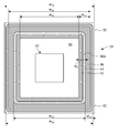
- FIG. 2 is a top view schematically showing the light emitting device 10 of FIG.
- the light emitting device 10 includes a light emitting element 20, a package substrate 30, a window member 40, and a sealing structure 50.
- the light emitting device 10 is an optical semiconductor device having a light emitting element 20 that is an optical semiconductor element.
- the light emitting element 20 is an LED (Light Emitting Diode) chip configured to emit “deep ultraviolet light” having a center wavelength ⁇ of about 360 nm or less.
- the light emitting element 20 is made of an aluminum gallium nitride (AlGaN) based semiconductor material having a band gap of about 3.4 eV or more.
- AlGaN aluminum gallium nitride
- the light emitting element 20 includes a semiconductor multilayer structure 22, a light emitting surface 24, a first element electrode 26, and a second element electrode 27.
- the semiconductor multilayer structure 22 includes a template layer, an n-type cladding layer, an active layer, a p-type cladding layer, and the like that are stacked on a substrate that becomes the light emitting surface 24.
- a sapphire (Al 2 O 3 ) substrate is used as a substrate that becomes the light emitting surface 24, and aluminum nitride (AlN) is used as a template layer of the semiconductor multilayer structure 22. Layers are used.
- the cladding layer and the active layer of the semiconductor multilayer structure 22 are made of an AlGaN-based semiconductor material.
- the first element electrode 26 and the second element electrode 27 are electrodes for supplying carriers to the active layer of the semiconductor multilayer structure 22, and each is an anode electrode or a cathode electrode.
- the first element electrode 26 and the second element electrode 27 are provided on the side opposite to the light emitting surface 24.
- the first element electrode 26 is attached to the first inner electrode 36 of the substrate 30, and the second element electrode 27 is attached to the second inner electrode 37 of the substrate 30.
- the package substrate 30 is a rectangular member having an upper surface 31 and a lower surface 32.
- the package substrate 30 is a ceramic substrate containing alumina (Al 2 O 3 ), aluminum nitride (AlN), or the like, and is a so-called high temperature fired ceramic multilayer substrate (HTCC, High Temperature Co-fired Ceramic).
- the upper surface 31 of the package substrate 30 is provided with a recess 34 for accommodating the light emitting element 20.
- a first inner electrode 36 and a second inner electrode 37 for attaching the light emitting element 20 are provided on the bottom surface of the recess 34.
- a first outer electrode 38 and a second outer electrode 39 for mounting the light emitting device 10 on an external substrate or the like are provided on the lower surface 32 of the package substrate 30.
- the window member 40 is a protective member provided so as to cover the opening of the recess 34.
- the ultraviolet light emitted from the light emitting element 20 is output from the outer surface 43 of the window member 40 to the outside of the package through the window member 40.
- the window member 40 includes a glass plate 42 and a frame body 46.
- the glass plate 42 has a rectangular shape, and four corners are rounded.
- the glass plate 42 is preferably made of a material having a high transmittance of deep ultraviolet light and a thermal expansion coefficient approximate to that of the frame body 46.
- the glass plate 42 is made of borate glass such as borosilicate glass.
- the glass plate 42 is formed thin so that the transmittance of deep ultraviolet light emitted from the light emitting element 20 is 80% or more, preferably 85% or more.
- the thickness t 1 of the glass plate 42 is, for example, 300 ⁇ m or less, and preferably about 150-200 ⁇ m.
- the glass plate 42 may be made of quartz glass having a high transmittance of deep ultraviolet light.
- the frame 46 is a so-called seal ring, is formed in a rectangular frame shape, and four corners are rounded.
- the frame 46 has the same outer dimensions as the glass plate 42 and has an inner shape that is larger than the recess 34 of the package substrate 30.
- the frame body 46 is provided on the inner surface 44 of the glass plate 42 and is attached along the outer periphery of the glass plate 42.
- the frame 46 is preferably made of a material having a thermal expansion coefficient close to that of the glass plate 42, and is preferably made of a Kovar alloy that is an iron-nickel-cobalt alloy, for example.
- the frame 46 has a lower surface 46a, an inner peripheral surface 46b, an outer peripheral surface 46c, and an upper surface 46d.
- the lower surface 46 a faces the upper surface 31 of the package substrate 30.
- the inner peripheral surface 46b is a side surface located between the lower surface 46a and the inner surface 44 of the glass plate 42 and exposed to the inside of the package.
- the outer peripheral surface 46c is a side surface exposed to the outside of the package.
- the upper surface 46d is joined to the inner surface 44 of the glass plate 42.
- the frame 46 is preferably formed to be thin to some extent so as not to block the output light of the light emitting element 20 output at a wide light distribution angle from the opening of the recess 34.
- the frame body 46 is formed to be thick to some extent.
- the thickness t 2 of the frame 46 for example, about 20 [mu] m-200 [mu] m, preferably approximately 50 [mu] m-150 [mu] m.
- the sealing structure 50 includes a first metal layer 51, a second metal layer 52, and a metal joint portion 53.
- the first metal layer 51 is provided in a frame shape on the upper surface 31 of the package substrate 30.
- the first metal layer 51 has a rectangular frame shape corresponding to the rectangular package substrate 30, and four corners are rounded.
- the first metal layer 51 is formed, for example, by a metallization process on a ceramic substrate.
- the first metal layer 51 is formed by plating a base material containing tungsten (W), molybdenum (Mo), or the like with nickel (Ni), gold (Au), or the like.
- the first metal layer 51 has a laminated structure of W / Ni / Au. Have.
- the first metal layer 51 is bonded to the metal bonding portion 53.
- the second metal layer 52 is provided on at least the lower surface 46a and the inner peripheral surface 46b of the frame 46.
- the second metal layer 52 may be provided on the outer peripheral surface 46c as illustrated.
- the second metal layer 52 is formed, for example, by performing plating after attaching the frame 46 to the glass plate 42.
- the second metal layer 52 may be a multilayer film in which nickel (Ni) and gold (Au) are sequentially laminated on the surface of the frame body 46.
- the second metal layer 52 is bonded to the metal bonding portion 53.
- the metal joint portion 53 is provided between the first metal layer 51 and the second metal layer 52, and joins and seals between the package substrate 30 and the window member 40 at the outer peripheral portion of the package.
- the metal joint portion 53 fills a space between the first metal layer 51 and the second metal layer 52, and a part thereof is provided on the inner peripheral surface 46 b of the frame body 46.
- the metal joint portion 53 is provided so as to form a fillet along the inner peripheral surface 46 b of the frame body 46.
- the metal joint portion 53 is made of a metal material having a low melting point, and includes, for example, an alloy of gold tin (AuSn) or silver tin (AgSn).
- the metal bonding part 53 spreads between the first metal layer 51 and the second metal layer 52 in a molten state to form a eutectic bond.
- the metal joint portion 53 is composed of gold tin with a tin (Sn) content of 20% to 24% wt so as to have high sealing reliability and a low melting temperature of 300 ° C. or less. Is preferred.
- FIG. 2 schematically shows the dimensions of the package substrate 30 and the window member 40.
- the outer dimension w 20 of the window member 40 (frame body 46) is smaller than the outer dimension w 10 of the package substrate 30.
- the outer dimension w 11 of the first metal layer 51 is smaller than the outer dimension w 20 of the frame 46, and the inner dimension w 12 of the first metal layer 51 is smaller than the inner dimension w 22 of the frame 46.
- the outer dimension w 10 of the package substrate 30 is 3.5 mm
- the outer dimension w 11 of the first metal layer 51 is 3.2 mm
- the inner dimension w 12 of the first metal layer 51 is 2. 3 mm
- the width w 13 of the first metal layer 51 is 0.45 mm
- external dimensions w 20 of the window member 40 is 3.4 mm
- inner dimensions w 22 of the frame 46 is 2.8 mm
- the width w 23 of the frame 46 is 0.3 mm.
- the thickness t 1 of the glass plate 42 is 170 [mu] m
- the thickness t2 of the frame 46 is 150 [mu] m.
- the inner shape dimensional difference between the first metal layer 51 and the frame 46 is 0.5 mm, and the inner shape of the first metal layer 51 (the outer periphery of the recess 34) and the inner peripheral surface 46b of the frame 46 are different.
- width w 3 between is 250 ⁇ m. Therefore, the width w 3 in the range where the frame body 46 does not overlap on the region of the first metal layer 51 is larger than the thickness t 2 of the frame body 46.
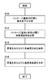
- FIG. 3 is a flowchart showing a method for manufacturing the light emitting device 10 according to the embodiment.
- the light emitting element 20 is accommodated in the recess 34 of the package substrate 30 (S10), the window member 40 is disposed so as to cover the opening of the recess 34, and metal bonding is performed between the upper surface 31 of the package substrate 30 and the lower surface 46a of the frame body 46.
- the material 56 (see FIG. 4 described later) is arranged (S12). Subsequently, the metal bonding material is heated to a molten state while applying a load between the package substrate 30 and the window member 40 (S14). Thereafter, the metal joint 53 is cooled and solidified while applying a load between the package substrate 30 and the window member 40 (S16).
- FIG. 4 is a cross-sectional view schematically showing a manufacturing process of the light emitting device 10 and shows a process of arranging the metal bonding material 56 and aligning the package substrate 30 and the window member 40.
- the package substrate 30 and the window member 40 are aligned so that the center positions of the package substrate 30 and the window member 40 are aligned.
- the package substrate 30 and the window member 40 may be aligned so that any of the four corners of the package substrate 30 and any of the four corners of the window member 40 are aligned.
- the center positions of the package substrate 30 and the window member 40 are displaced within a range of ⁇ 50 ⁇ m. It can arrange
- a metal bonding material 56 is disposed between the aligned upper surface 31 of the package substrate 30 and the lower surface 46 a of the frame 46.
- the metal bonding material 56 is a gold-tin preform having a rectangular frame shape corresponding to a region where the upper surface 31 of the package substrate 30 and the lower surface 46a of the frame 46 are bonded.
- the metal bonding material 56 has an inner shape dimension and an outer dimension smaller than those of the first metal layer 51. For example, the outer dimension is 3.0 mm, and the inner dimension is 2.6 mm.
- the metal bonding material 56 may be temporarily fixed to the first metal layer 51 or the second metal layer 52 in advance.
- the thickness of the metal bonding material 56 is about 10 ⁇ m to 50 ⁇ m, preferably about 15 ⁇ m to 30 ⁇ m.
- a metal joint 53 having a thickness of about 5 ⁇ m to 20 ⁇ m can be formed.
- the load 60 applied at the time of sealing is 50 g or more, preferably 100 g or more, more preferably 200 g or more.
- the metal bonding material 56 is heated and melted while applying a load 60 and spreads between the first metal layer 51 and the second metal layer 52.
- the metal bonding material 56 spreads in the horizontal direction along the first metal layer 51 and spreads in the vertical direction along the second metal layer 52 provided on the inner peripheral surface 46 b of the frame body 46. Therefore, a part of the metal bonding material 56 extends toward the inner surface 44 of the glass plate 42 along the inner peripheral surface 46b of the frame 46 to form a fillet on the inner peripheral surface 46b.
- the step of heating and melting the metal bonding material 56 is preferably performed in an atmosphere of an inert gas such as nitrogen (N 2 ).
- an inert gas such as nitrogen (N 2 ).
- the gold-tin preform in a molten state can be prevented from being oxidized, and an inert gas can be filled into the package.
- the heating and melting step according to the present embodiment may be performed in an atmosphere of dry air containing oxygen (O 2 ).
- FIG. 5 is a cross-sectional view schematically showing a light emitting device 110 according to a comparative example.
- the frame member 146 is formed so as to surround the outer periphery of the glass plate 142, and the window member 140 is configured such that the inner surface 144 of the glass plate 142 and the lower surface 146a of the frame member 146 form one flat surface. This is different from the above-described embodiment.
- the first metal layer 51 formed on the package substrate 30 and the frame body 146 of the window member 140 are joined by a metal joint portion 153.
- a protruding portion 154 is formed in which a part of the metal bonding material protrudes into the inside of the package and solidifies into a spherical shape.
- the overhanging portion 154 is formed by extruding a part of the metal bonding material from between the package substrate 30 and the window member 140 when bonding between the package substrate 30 and the window member 140 while applying a load.
- a part of the deep ultraviolet light emitted from the light emitting element 20 is shielded by the overhang portion 154, which may lead to a decrease in light extraction efficiency to the outside.
- the metal bonding material flows out to the mounting surface of the recess 34 without staying on the inner surface 144 of the window member 140 as the overhanging portion 154, it may lead to a short circuit between the first inner electrode 36 and the second inner electrode 37. There is.
- the amount of the gold-tin preform is reduced so that a part of the metal bonding material does not protrude, bonding with high sealing reliability may not be possible.
- the upper surface 31 of the package substrate 30 is not necessarily a completely flat surface due to manufacturing reasons and the like, and since there are fine irregularities depending on the location, the amount of bonding material on a part of the upper surface 31 of the package substrate 30 is large. It may not be properly sealed and joined.
- the inner peripheral surface 46b of the frame body 46 is positioned on the first metal layer 51, the metal that protrudes from between the first metal layer 51 and the lower surface 46a of the frame body 46.
- the bonding material can be extended vertically upward toward the glass plate 42. Thereby, it can prevent that a metal joining material extends
- the thickness t 2 of the frame body 46 by making the thickness t 2 of the frame body 46 and 20 ⁇ m or 200 ⁇ m or less, a decrease in light extraction efficiency due to the thickness of the effects and the frame 46 for preventing the falling of the metal bonding material Both preventive effects can be achieved. If the thickness of the frame body 46 is larger than 200 ⁇ m, a part of deep ultraviolet light output from the light emitting element 20 at a wide light distribution angle (for example, 150 degrees) is blocked by the frame body 46. . Further, when the thickness t 2 of the frame 46 is smaller than 20 [mu] m, narrows the space for absorbing the protrusion of the metal bonding material, there may not be sufficiently prevented rundown of the metal bonding material. On the other hand, according to this embodiment, by appropriately adjusting the thickness t 2 of the frame 46, it is possible to achieve sealing reliability, improved manufacturing yield and light extraction efficiency.
- the present embodiment by visually confirming the fillet formed on the inner peripheral surface 46b of the frame 46, it is possible to easily carry out an inspection of whether or not the sealing joint is appropriately performed. Since the fillet on the inner peripheral surface 46b is formed by protruding from between the upper surface 31 of the package substrate 30 and the lower surface 46a of the frame body 46, a metal bonding material is filled between the upper surface 31 and the lower surface 46a by the fillet. Can be confirmed. On the other hand, if the fillet is not formed on the inner peripheral surface 46b, it is suggested that the metal bonding material is not filled between the upper surface 31 and the lower surface 46a, and the reliable sealing bonding is not performed. Therefore, according to the present embodiment, it is possible to easily check the sealing performance by confirming whether the fillet is formed over the entire circumference along the inner circumferential surface 46 b of the frame body 46 using an image recognition technique or the like.
- the case where only the light emitting element is included in the package of the light emitting device is shown.
- an electronic component other than the light emitting element may be incorporated in the package in order to provide an additional function.
- a Zener diode for protecting the light emitting element from an electrical surge may be incorporated in the housing.
- a phosphor for converting the wavelength of light output from the light emitting element may be incorporated, or an optical element for controlling the orientation of light emitted from the light emitting element may be incorporated.
- the light-emitting device in which the semiconductor light-emitting element is sealed in the package has been described.
- the above-described sealing structure may be used to seal the light receiving element.
- the above-described package structure may be used for sealing a light receiving element for receiving deep ultraviolet light. That is, the package may be used for sealing an optical semiconductor element.
- DESCRIPTION OF SYMBOLS 10 ... Light-emitting device, 20 ... Light emitting element, 30 ... Package board
- the reliability of an optical semiconductor device having a semiconductor optical semiconductor element can be improved.
Landscapes
- Led Device Packages (AREA)
Abstract
発光装置10は、上面31に開口する凹部34を有するパッケージ基板30と、凹部34に収容される発光素子20と、凹部34の開口を覆うように配置される窓部材40と、パッケージ基板30と窓部材40の間を封止する封止構造50と、を備える。窓部材40は、発光素子20に対向する内面44を有するガラス板42と、ガラス板42の内面44上に設けられる枠体46とを有する。封止構造50は、パッケージ基板30の上面31に枠状に設けられる第1金属層51と、枠体46の下面46aおよび内周面46bに設けられる第2金属層52と、第1金属層51と第2金属層52の間に設けられる金属接合部53とを有し、金属接合部53の少なくとも一部が内周面46b上に設けられる。
Description
本発明は、光半導体装置に関し、特に、半導体光半導体素子を有する光半導体装置に関する。
近年、青色光を出力する発光ダイオードやレーザダイオード等の半導体発光素子が実用化されており、さらに波長の短い深紫外光を出力する発光素子の開発が進められている。深紫外光は高い殺菌能力を有することから、深紫外光の出力が可能な半導体発光素子は、医療や食品加工の現場における水銀フリーの殺菌用光源として注目されている。また、出力波長を問わず、より発光強度の高い半導体発光素子の開発が進められている。
発光素子は、外部環境から素子を保護するためのパッケージ内に収容される。例えば、発光素子が実装される基板と、その基板上に配置される蓋体とを接合することで発光素子が封止される。蓋体は、金属枠体の開口部に透光性の窓部材が嵌め込まれ、基板の外周には金属製のシールリングが設けられ、金属枠体とシールリングの間でろう材を介して取り付けされる(例えば、特許文献1参照)。
基板と蓋体をろう材を介して接合する際、接合性を向上させるために基板と蓋体の間でろう材に荷重をかけながら封止することが望ましい。このとき、基板と蓋体の間から押し出されたろう材の一部が発光素子の実装面に向けて流れ出してしまうと、配線間をショートさせてしまい、製造歩留まりを低下させてしまう懸念がある。
本発明はこうした課題に鑑みてなされたものであり、その例示的な目的のひとつは、光半導体装置の信頼性および製造歩留まりを向上させる技術を提供することにある。
本発明のある態様の光半導体装置は、上面に開口する凹部を有するパッケージ基板と、凹部に収容される光半導体素子と、凹部の開口を覆うように配置される窓部材と、パッケージ基板と窓部材の間を封止する封止構造と、を備える。窓部材は、光半導体素子に対向する内面を有するガラス板と、ガラス板の内面上に設けられる枠体とを有する。封止構造は、パッケージ基板の上面に枠状に設けられる第1金属層と、枠体の下面および内周面に設けられる第2金属層と、第1金属層と第2金属層の間に設けられる金属接合部とを有し、金属接合部の少なくとも一部が内周面上に設けられる。
この態様によると、枠体の内周面に金属層が設けられているため、パッケージ基板の上面と枠体の間で荷重をかけながら金属接合部を形成する際、下面と枠体の間から押し出される接合材が枠体の内周面に沿って上方向に延伸するようになる。その結果、押し出された接合材が基板の凹部に向けて流れ出すことを防ぎ、枠体の近傍に接合材を留めることができる。これにより、接合時の製造歩留まりを向上させるとともに、荷重を加えた接合プロセスによって信頼性の高い封止構造を実現できる。
枠体の外形寸法はパッケージ基板の外形寸法より小さく、枠体の内形寸法はパッケージ基板の凹部の内形寸法より大きい。
枠体は、下面からガラス板の内面までの高さが10μm以上200μm以下であってもよい。
光半導体素子は、深紫外光を発する発光素子であってよく、窓部材は、深紫外光の透過率が80%以上となるよう構成されてもよい。
ガラス板は、厚さが300μm以下のホウ酸塩ガラスで構成され、枠体は、コバール合金で構成され、金属接合部は、金錫(AuSn)を含んでもよい。
本発明の別の態様は、光半導体装置の製造方法である。この方法は、上面に開口する凹部を有するパッケージ基板の凹部に光半導体素子を収容するステップと、凹部の開口を覆うように窓部材を配置するステップと、パッケージ基板と窓部材の間を封止するステップと、を備える。窓部材は、光半導体素子に対向する内面を有するガラス板と、ガラス板の内面上に設けられる枠体とを有する。パッケージ基板の上面には枠状の第1金属層が設けられており、枠体の下面および内周面には第2金属層が設けられており、封止するステップは、パッケージ基板と窓部材の間で荷重を加えながら第1金属層と第2金属層の間に配置される金属接合材を加熱するステップを含む。
この態様によると、枠体の内周面に金属層が設けられているため、パッケージ基板の上面と枠体の間で荷重をかけながら金属接合材を加熱溶融させる際、下面と枠体の間から押し出される金属接合材が枠体の内周面に沿って上方向に延伸するようになる。その結果、押し出された金属接合材が基板の凹部に向けて流れ出すことを防ぎ、枠体の近傍に金属接合材を留めることができる。これにより、接合時の製造歩留まりを向上させるとともに、荷重を加えた接合プロセスによって信頼性の高い封止構造を実現することができる。
封止するステップは、金属接合材の加熱後にパッケージ基板と窓部材の間で荷重を加えながら金属接合材を冷却するステップを含んでもよい。
金属接合材は、枠体の下面に対応した枠形状を有する金錫(AuSn)の金属板であってもよい。
本発明によれば、半導体光半導体素子を有する光半導体装置の信頼性を高めることができる。
以下、図面を参照しながら、本発明を実施するための形態について詳細に説明する。説明において同一の要素には同一の符号を付し、重複する説明を適宜省略する。説明の理解を助けるため、各図面における各構成要素の寸法比は必ずしも実際の装置の寸法比と一致しない。
図1は、実施の形態に係る発光装置10を概略的に示す断面図であり、図2は、図1の発光装置10を概略的に示す上面図である。発光装置10は、発光素子20と、パッケージ基板30と、窓部材40と、封止構造50とを備える。発光装置10は、光半導体素子である発光素子20を有する光半導体装置である。
発光素子20は、中心波長λが約360nm以下となる「深紫外光」を発するように構成されるLED(Light Emitting Diode)チップである。このような波長の深紫外光を出力するため、発光素子20は、バンドギャップが約3.4eV以上となる窒化アルミニウムガリウム(AlGaN)系半導体材料で構成される。本実施の形態では、特に、中心波長λが約240nm~350nmの深紫外光を発する場合について示す。
発光素子20は、半導体積層構造22と、光出射面24と、第1素子電極26と、第2素子電極27とを有する。
半導体積層構造22は、光出射面24となる基板上に積層されるテンプレート層、n型クラッド層、活性層、p型クラッド層などを含む。発光素子20が深紫外光を出力するように構成される場合、光出射面24となる基板としてサファイア(Al2O3)基板が用いられ、半導体積層構造22のテンプレート層として窒化アルミニウム(AlN)層が用いられる。また、半導体積層構造22のクラッド層や活性層はAlGaN系半導体材料で構成される。
第1素子電極26および第2素子電極27は、半導体積層構造22の活性層にキャリアを供給するための電極であり、それぞれがアノード電極またはカソード電極である。第1素子電極26および第2素子電極27は、光出射面24と反対側に設けられる。第1素子電極26は、基板30の第1内側電極36に取り付けられ、第2素子電極27は、基板30の第2内側電極37に取り付けられる。
パッケージ基板30は、上面31と下面32を有する矩形状の部材である。パッケージ基板30は、アルミナ(Al2O3)や窒化アルミニウム(AlN)などを含むセラミック基板であり、いわゆる高温焼成セラミック多層基板(HTCC、High Temperature Co-fired Ceramic)である。
パッケージ基板30の上面31には、発光素子20を収容するための凹部34が設けられる。凹部34の底面には、発光素子20を取り付けるための第1内側電極36および第2内側電極37が設けられる。パッケージ基板30の下面32には、発光装置10を外部基板などに実装するための第1外側電極38および第2外側電極39が設けられる。
窓部材40は、凹部34の開口を覆うように設けられる保護部材である。発光素子20が発する紫外光は、窓部材40を介して窓部材40の外面43からパッケージの外部へと出力される。窓部材40は、ガラス板42と、枠体46とを有する。
ガラス板42は、矩形状を有し、四隅がR面取りされている。ガラス板42は、深紫外光の透過率が高く、枠体46と熱膨張係数が近似した材料で構成されることが好ましい。ガラス板42は、例えばホウ珪酸ガラスなどのホウ酸塩ガラスで構成される。ガラス板42は、発光素子20が発する深紫外光の透過率が80%以上、好ましくは85%以上となるように薄く形成される。ガラス板42の厚さt1は、例えば300μm以下であり、150-200μm程度であることが好ましい。ガラス板42は、深紫外光の透過率が高い石英ガラスで構成されてもよい。
枠体46は、いわゆるシールリングであり、矩形枠状に形成され、四隅がR面取りされている。枠体46は、ガラス板42と同じ外形寸法を有し、パッケージ基板30の凹部34よりも大きい内形寸法を有する。枠体46は、ガラス板42の内面44上に設けられ、ガラス板42の外周に沿って取り付けられる。枠体46は、ガラス板42と熱膨張係数が近似した材料であることが好ましく、例えば、鉄-ニッケル-コバルト合金であるコバール合金で構成されることが望ましい。
枠体46は、下面46aと、内周面46bと、外周面46cと、上面46dとを有する。下面46aは、パッケージ基板30の上面31と対向する。内周面46bは、下面46aとガラス板42の内面44の間に位置し、パッケージの内側に露出する側面である。外周面46cは、パッケージの外側に露出する側面である。上面46dは、ガラス板42の内面44と接合されている。
枠体46は、凹部34の開口から広配光角で出力される発光素子20の出力光を遮らないようにある程度薄く形成されることが好ましい。一方で、枠体46の内周面46bの高さを確保するためにある程度厚く形成されることが好ましい。枠体46の厚さt2は、例えば20μm-200μm程度であり、好ましくは50μm-150μm程度である。
封止構造50は、第1金属層51と、第2金属層52と、金属接合部53とを有する。
第1金属層51は、パッケージ基板30の上面31に枠状に設けられる。第1金属層51は、矩形のパッケージ基板30に対応した矩形枠形状を有し、四隅がR面取りされている。第1金属層51は、例えばセラミック基板へのメタライズ処理により形成される。第1金属層51は、タングステン(W)やモリブデン(Mo)等を含む基材にニッケル(Ni)や金(Au)等がメッキされて形成され、例えば、W/Ni/Auの積層構造を有する。第1金属層51は、金属接合部53と接合される。
第2金属層52は、枠体46の少なくとも下面46aおよび内周面46bに設けられる。第2金属層52は、図示されるように外周面46cに設けられてもよい。第2金属層52は、例えば、枠体46をガラス板42に取り付けた後にめっき処理を施すことにより形成される。第2金属層52は、枠体46の表面上にニッケル(Ni)、金(Au)が順に積層される多層膜であってもよい。第2金属層52は、金属接合部53と接合される。
金属接合部53は、第1金属層51と第2金属層52の間に設けられ、パッケージの外周部においてパッケージ基板30と窓部材40の間を接合して封止する。金属接合部53は、第1金属層51と第2金属層52の間を充填するとともに、その一部が枠体46の内周面46b上に設けられる。金属接合部53は、枠体46の内周面46bに沿ってフィレットを形成するように設けられる。
金属接合部53は、低融点の金属材料で構成され、例えば金錫(AuSn)や銀錫(AgSn)の合金を含む。金属接合部53は、溶融状態において第1金属層51と第2金属層52の間に広がって共晶接合を形成する。金属接合部53は、高い封止信頼性を有するとともに溶融温度が300℃以下の低温となるように、錫(Sn)の含有量が20%wt~24%wtの金錫で構成されることが好ましい。
図2は、パッケージ基板30および窓部材40の寸法を概略的に示す。図示されるように、窓部材40(枠体46)の外形寸法w20は、パッケージ基板30の外形寸法w10より小さい。第1金属層51の外形寸法w11は、枠体46の外形寸法w20より小さく、第1金属層51の内形寸法w12は、枠体46の内形寸法w22より小さい。
ある実施例において、パッケージ基板30の外形寸法w10は3.5mmであり、第1金属層51の外形寸法w11は3.2mmであり、第1金属層51の内形寸法w12は2.3mmであり、第1金属層51の幅w13は0.45mmである。また、窓部材40の外形寸法w20は3.4mmであり、枠体46の内形寸法w22は2.8mmであり、枠体46の幅w23は0.3mmである。また、ガラス板42の厚さt1は170μmであり、枠体46の厚さt2は150μmである。この実施例において、第1金属層51と枠体46の内形寸法差は0.5mmであり、第1金属層51の内形(凹部34の外周)と枠体46の内周面46bの間の幅w3は250μmである。したがって、第1金属層51の領域上で枠体46が重畳していない範囲の幅w3は、枠体46の厚さt2より大きい。
つづいて、発光装置10の製造方法について説明する。
図3は、実施の形態に係る発光装置10の製造方法を示すフローチャートである。パッケージ基板30の凹部34に発光素子20を収容し(S10)、凹部34の開口を覆うように窓部材40を配置し、パッケージ基板30の上面31と枠体46の下面46aの間に金属接合材56(後述の図4参照)が配置されるようにする(S12)。つづいて、パッケージ基板30と窓部材40の間で荷重をかけながら金属接合材を加熱して溶融状態とする(S14)。その後、パッケージ基板30と窓部材40の間で荷重をかけながら金属接合部53を冷却して固化させる(S16)。
図3は、実施の形態に係る発光装置10の製造方法を示すフローチャートである。パッケージ基板30の凹部34に発光素子20を収容し(S10)、凹部34の開口を覆うように窓部材40を配置し、パッケージ基板30の上面31と枠体46の下面46aの間に金属接合材56(後述の図4参照)が配置されるようにする(S12)。つづいて、パッケージ基板30と窓部材40の間で荷重をかけながら金属接合材を加熱して溶融状態とする(S14)。その後、パッケージ基板30と窓部材40の間で荷重をかけながら金属接合部53を冷却して固化させる(S16)。
図4は、発光装置10の製造工程を概略的に示す断面図であり、金属接合材56を配置してパッケージ基板30および窓部材40を位置合わせする工程を示している。パッケージ基板30および窓部材40は、例えば、パッケージ基板30と窓部材40の中心位置が揃うように位置合わせされる。パッケージ基板30および窓部材40は、パッケージ基板30の四隅のいずれかと窓部材40の四隅のいずれかが揃うように位置合わせしてもよい。この場合、上述した寸法の実施例によれば、パッケージ基板30と窓部材40の中心位置が±50μmの範囲でずれてしまうが、そのずれがあったとしても、第1金属層51の上に枠体46の内周面46bが位置するように配置できる。
位置合わせされたパッケージ基板30の上面31と枠体46の下面46aの間には金属接合材56が配置される。金属接合材56は、パッケージ基板30の上面31と枠体46の下面46aが接合される領域に対応した矩形枠形状を有する金錫のプリフォームである。金属接合材56は、第1金属層51より小さい内形寸法および外形寸法を有し、例えば、外形寸法が3.0mm、内形寸法が2.6mmである。金属接合材56は、第1金属層51または第2金属層52にあらかじめ仮止めされていてもよい。金属接合材56の厚さは10μm~50μm程度であり、好ましくは15μm~30μm程度である。このような形状および厚さのプリフォームを用いて荷重60をかけながら封止することで、厚さが5μm~20μm程度の金属接合部53を形成することができる。なお、封止時に加える荷重60は50g以上であり、好ましくは100g以上、より好ましくは200g以上である。
金属接合材56は荷重60をかけながら加熱溶融され、第1金属層51と第2金属層52の間で広がっていく。金属接合材56は、第1金属層51に沿って水平方向に広がるとともに、枠体46の内周面46b上に設けられる第2金属層52に沿って鉛直方向に広がる。したがって、金属接合材56の一部は、枠体46の内周面46bに沿ってガラス板42の内面44に向かって延伸して内周面46b上にフィレットを形成する。
金属接合材56を加熱溶融させる工程は、窒素(N2)などの不活性ガスの雰囲気下でなされることが好ましい。これにより、溶融状態となった金錫プリフォームの酸化を防ぐとともに、パッケージの内部に不活性ガスを充填できる。しかしながら、本実施の形態に係る加熱溶融工程は、酸素(O2)を含む乾燥空気の雰囲気下でなされてもよい。荷重をかけながら金錫プリフォームを加熱溶融させることで、第1金属層51と第2金属層52の間での金属接合材56の酸化を防ぎつつ封止することが可能となる。
つづいて、本実施の形態が奏する効果について比較例を参照しながら説明する。
図5は、比較例に係る発光装置110を概略的に示す断面図である。本比較例では、ガラス板142の外周を囲むように枠体146が形成され、ガラス板142の内面144と枠体146の下面146aとが一つの平坦面を形成するように窓部材140が構成される点で上述の実施の形態と相違する。パッケージ基板30に形成される第1金属層51と窓部材140の枠体146の間は、金属接合部153により接合されている。
図5は、比較例に係る発光装置110を概略的に示す断面図である。本比較例では、ガラス板142の外周を囲むように枠体146が形成され、ガラス板142の内面144と枠体146の下面146aとが一つの平坦面を形成するように窓部材140が構成される点で上述の実施の形態と相違する。パッケージ基板30に形成される第1金属層51と窓部材140の枠体146の間は、金属接合部153により接合されている。
本比較例では、図示されるように、金属接合材の一部がパッケージの内側にはみ出して球状に固化した張出部154が形成されている。張出部154は、パッケージ基板30と窓部材140の間を荷重をかけながら接合する際、パッケージ基板30と窓部材140の間から金属接合材の一部が押し出されることにより形成される。このような張出部154が形成されると、発光素子20が発する深紫外光の一部が張出部154に遮蔽され、外部への光取出効率の低下につながりうる。また、張出部154として窓部材140の内面144に留まらずに凹部34の実装面に金属接合材が流れ出してしまうと、第1内側電極36と第2内側電極37の間のショートにつながるおそれがある。一方で、金属接合材の一部がはみ出ないように金錫プリフォームの量を減らしてしまうと、封止信頼性の高い接合ができなくなるおそれがある。製造上の都合等によりパッケージ基板30の上面31は完全な平坦面であるとは限らず、場所に応じて微細な凹凸があるため、パッケージ基板30の上面31の一部で接合材の量が不足して適切に封止接合されないかもしれない。
一方、本実施の形態によれば、第1金属層51の上に枠体46の内周面46bが位置するため、第1金属層51と枠体46の下面46aとの間からはみ出した金属接合材をガラス板42に向けて鉛直上方向に延伸させることができる。これにより、金属接合材が水平方向にのみ延伸して張出部154を形成したり、凹部34の内部に流れ落ちたりすることを防ぐことができる。したがって、本実施の形態によれば、製造不良による歩留低下を防ぎつつ、封止に十分な量の金属接合材を用いて荷重をかけながら信頼性の高い封止接合を実現することができる。
本実施の形態によれば、枠体46の厚さt2を20μm以上200μm以下とすることにより、金属接合材の落下を防止する効果と枠体46の厚みに起因する光取出効率の低下を防止する効果の双方を両立できる。仮に、枠体46の厚さを200μmより大きくしてしまうと、広配光角(例えば、150度)で発光素子20から出力される深紫外光の一部が枠体46によって遮蔽されてしまう。また、枠体46の厚さt2を20μmより小さくすると、金属接合材のはみ出しを吸収するための空間が狭くなり、金属接合材の流れ落ちを十分に防止できないおそれがある。一方、本実施の形態によれば、枠体46の厚さt2を適切に調整することにより、封止信頼性、製造歩留および光取出効率の向上を実現することができる。
本実施の形態によれば、枠体46の内周面46bに形成されるフィレットを目視で確認することにより、封止接合が適切になされているかの検査を簡易的に実施できる。内周面46b上のフィレットは、パッケージ基板30の上面31と枠体46の下面46aの間からのはみ出しにより形成されるため、フィレットにより上面31と下面46aの間に金属接合材が充填されていることを確認できる。一方、内周面46b上にフィレットが形成されていなければ、上面31と下面46aの間に金属接合材が充填されておらず、確実な封止接合がなされていないことが示唆される。したがって、本実施の形態によれば、フィレットが枠体46の内周面46bに沿って全周にわたって形成されているかを画像認識技術等を用いて確認することで封止性を簡易検査できる。
以上、本発明を実施の形態にもとづいて説明した。本発明は上記実施の形態に限定されず、種々の設計変更が可能であり、様々な変形例が可能であること、またそうした変形例も本発明の範囲にあることは、当業者に理解されるところである。
上述の実施の形態および変形例では、発光装置のパッケージ内に発光素子のみを含める場合を示した。さらなる変形例においては、付加的な機能を持たせるために発光素子以外の電子部品をパッケージ内に組み込むこととしてもよい。例えば、電気的サージから発光素子を保護するためのツェナーダイオードを筐体内に組み込むこととしてもよい。また、発光素子が出力する光の波長を変換するための蛍光体を組み込んでもよいし、発光素子が発する光の配向を制御するための光学素子を組み込んでもよい。
上述の実施の形態および変形例では、半導体発光素子をパッケージ内に封止した発光装置について示した。さらなる変形例においては、受光素子を封止するために上述の封止構造を用いてもよい。例えば、深紫外光を受光するための受光素子の封止に上述のパッケージ構造を用いてもよい。つまり、上記パッケージを光半導体素子の封止に用いてもよい。
10…発光装置、20…発光素子、30…パッケージ基板、31…上面、34…凹部、40…窓部材、42…ガラス板、44…内面、46…枠体、46a…下面、46b…内周面、50…封止構造、51…第1金属層、52…第2金属層、53…金属接合部、56…金属接合材、60…荷重。
本発明によれば、半導体光半導体素子を有する光半導体装置の信頼性を高めることができる。
Claims (8)
- 上面に開口する凹部を有するパッケージ基板と、
前記凹部に収容される光半導体素子と、
前記凹部の開口を覆うように配置される窓部材と、
前記パッケージ基板と前記窓部材の間を封止する封止構造と、を備え、
前記窓部材は、前記光半導体素子に対向する内面を有するガラス板と、前記ガラス板の前記内面上に設けられる枠体とを有し、
前記封止構造は、前記パッケージ基板の前記上面に枠状に設けられる第1金属層と、前記枠体の下面および内周面に設けられる第2金属層と、前記第1金属層と前記第2金属層の間に設けられる金属接合部とを有し、前記金属接合部の少なくとも一部が前記内周面上に設けられることを特徴とする光半導体装置。 - 前記枠体の外形寸法は前記パッケージ基板の外形寸法より小さく、前記枠体の内形寸法は前記パッケージ基板の前記凹部の内形寸法より大きいことを特徴とする請求項1に記載の光半導体装置。
- 前記枠体は、前記下面から前記ガラス板の前記内面までの高さが10μm以上200μm以下であることを特徴とする請求項1または2に記載の光半導体装置。
- 前記光半導体素子は、深紫外光を発する発光素子であり、前記窓部材は、前記深紫外光の透過率が80%以上となるよう構成されることを特徴とする請求項1から3のいずれか一項に記載の光半導体装置。
- 前記ガラス板は、厚さが300μm以下のホウ酸塩ガラスで構成され、
前記枠体は、コバール合金で構成され、
前記金属接合部は、金錫(AuSn)を含むことを特徴とする請求項1から4のいずれか一項に記載の光半導体装置。 - 上面に開口する凹部を有するパッケージ基板の前記凹部に光半導体素子を収容するステップと、
前記凹部の開口を覆うように窓部材を配置するステップと、
前記パッケージ基板と前記窓部材の間を封止するステップと、を備え、
前記窓部材は、前記光半導体素子に対向する内面を有するガラス板と、前記ガラス板の前記内面上に設けられる枠体とを有し、
前記パッケージ基板の前記上面には枠状の第1金属層が設けられており、
前記枠体の下面および内周面には第2金属層が設けられており、
前記封止するステップは、前記パッケージ基板と前記窓部材の間で荷重を加えながら前記第1金属層と前記第2金属層の間に配置される金属接合材を加熱するステップを含むことを特徴とする光半導体装置の製造方法。 - 前記封止するステップは、前記金属接合材の加熱後に前記パッケージ基板と前記窓部材の間で荷重を加えながら前記金属接合材を冷却するステップを含むことを特徴とする請求項6に記載の光半導体装置の製造方法。
- 前記金属接合材は、前記枠体の前記下面に対応した枠形状を有する金錫(AuSn)の金属板であることを特徴とする請求項6または7に記載の光半導体装置の製造方法。
Priority Applications (2)
| Application Number | Priority Date | Filing Date | Title |
|---|---|---|---|
| CN201780050482.3A CN110521011B (zh) | 2016-09-01 | 2017-08-10 | 光半导体装置及光半导体装置的制造方法 |
| US16/284,310 US11217730B2 (en) | 2016-09-01 | 2019-02-25 | Optical semiconductor apparatus and method of manufacturing optical semiconductor apparatus |
Applications Claiming Priority (2)
| Application Number | Priority Date | Filing Date | Title |
|---|---|---|---|
| JP2016-171231 | 2016-09-01 | ||
| JP2016171231A JP6294418B2 (ja) | 2016-09-01 | 2016-09-01 | 光半導体装置および光半導体装置の製造方法 |
Related Child Applications (1)
| Application Number | Title | Priority Date | Filing Date |
|---|---|---|---|
| US16/284,310 Continuation US11217730B2 (en) | 2016-09-01 | 2019-02-25 | Optical semiconductor apparatus and method of manufacturing optical semiconductor apparatus |
Publications (1)
| Publication Number | Publication Date |
|---|---|
| WO2018043095A1 true WO2018043095A1 (ja) | 2018-03-08 |
Family
ID=61309396
Family Applications (1)
| Application Number | Title | Priority Date | Filing Date |
|---|---|---|---|
| PCT/JP2017/029116 Ceased WO2018043095A1 (ja) | 2016-09-01 | 2017-08-10 | 光半導体装置および光半導体装置の製造方法 |
Country Status (5)
| Country | Link |
|---|---|
| US (1) | US11217730B2 (ja) |
| JP (1) | JP6294418B2 (ja) |
| CN (1) | CN110521011B (ja) |
| TW (1) | TWI659544B (ja) |
| WO (1) | WO2018043095A1 (ja) |
Cited By (1)
| Publication number | Priority date | Publication date | Assignee | Title |
|---|---|---|---|---|
| EP3664166A1 (en) * | 2018-12-05 | 2020-06-10 | Lite-On Opto Technology (Changzhou) Co., Ltd. | Light emitting package structure and method of manufacturing the same |
Families Citing this family (13)
| Publication number | Priority date | Publication date | Assignee | Title |
|---|---|---|---|---|
| JP6687008B2 (ja) | 2017-11-30 | 2020-04-22 | 日亜化学工業株式会社 | 発光装置 |
| JP6871184B2 (ja) * | 2018-01-31 | 2021-05-12 | 日機装株式会社 | 半導体発光装置の製造方法 |
| JP7414553B2 (ja) | 2019-01-30 | 2024-01-16 | 浜松ホトニクス株式会社 | 光学ユニット |
| JP2021012961A (ja) * | 2019-07-08 | 2021-02-04 | スタンレー電気株式会社 | 発光装置、および、その製造方法 |
| JP7136358B2 (ja) * | 2019-07-25 | 2022-09-13 | 株式会社大真空 | 発光装置のリッド材およびリッド材の製造方法 |
| JP7370274B2 (ja) * | 2020-02-18 | 2023-10-27 | 日機装株式会社 | 半導体パッケージ及び半導体発光装置 |
| CN113394320B (zh) | 2020-03-11 | 2023-04-07 | 隆达电子股份有限公司 | 发光二极管封装结构 |
| CN119630152A (zh) * | 2020-03-31 | 2025-03-14 | 光宝光电(常州)有限公司 | 封装结构 |
| JP7455003B2 (ja) * | 2020-06-09 | 2024-03-25 | スタンレー電気株式会社 | 半導体発光装置、および、水殺菌装置 |
| JP7510810B2 (ja) * | 2020-07-20 | 2024-07-04 | スタンレー電気株式会社 | 半導体発光装置 |
| TWI742904B (zh) * | 2020-10-30 | 2021-10-11 | 國立中正大學 | 廣角紫外線發光二極體之封裝結構 |
| JP7498799B2 (ja) * | 2020-12-18 | 2024-06-12 | Ngkエレクトロデバイス株式会社 | パッケージ |
| JP7523345B2 (ja) * | 2020-12-25 | 2024-07-26 | スタンレー電気株式会社 | 半導体装置及びその製造方法 |
Citations (4)
| Publication number | Priority date | Publication date | Assignee | Title |
|---|---|---|---|---|
| JPS6010757A (ja) * | 1983-06-30 | 1985-01-19 | Nec Corp | 半導体装置の製造方法 |
| JPH06204352A (ja) * | 1992-12-25 | 1994-07-22 | Ngk Spark Plug Co Ltd | 半導体セラミックパッケージ用基体及び蓋体 |
| US20150014711A1 (en) * | 2012-01-11 | 2015-01-15 | Osram Gmbh | Optoelectronic component with inert gas atmosphere |
| JP2015018873A (ja) * | 2013-07-09 | 2015-01-29 | 日機装株式会社 | 半導体モジュール |
Family Cites Families (7)
| Publication number | Priority date | Publication date | Assignee | Title |
|---|---|---|---|---|
| JP2005191314A (ja) | 2003-12-25 | 2005-07-14 | Kyocera Corp | 蓋体およびこれを用いた光半導体装置 |
| JP2007317816A (ja) * | 2006-05-25 | 2007-12-06 | Matsushita Electric Works Ltd | 発光装置 |
| KR101516358B1 (ko) * | 2012-03-06 | 2015-05-04 | 삼성전자주식회사 | 발광 장치 |
| KR102025424B1 (ko) * | 2012-12-03 | 2019-09-25 | 서울바이오시스 주식회사 | 다기능 발광다이오드 조명 장치 |
| CN203895492U (zh) * | 2014-04-10 | 2014-10-22 | 广州市鸿利光电股份有限公司 | 一种led分立式器件支架 |
| CN110931622A (zh) * | 2016-03-14 | 2020-03-27 | 光宝光电(常州)有限公司 | 发光二极管封装结构 |
| CN205488214U (zh) * | 2016-04-16 | 2016-08-17 | 陈春红 | 新型led封装结构 |
-
2016
- 2016-09-01 JP JP2016171231A patent/JP6294418B2/ja active Active
-
2017
- 2017-08-10 WO PCT/JP2017/029116 patent/WO2018043095A1/ja not_active Ceased
- 2017-08-10 CN CN201780050482.3A patent/CN110521011B/zh active Active
- 2017-08-25 TW TW106128983A patent/TWI659544B/zh active
-
2019
- 2019-02-25 US US16/284,310 patent/US11217730B2/en active Active
Patent Citations (4)
| Publication number | Priority date | Publication date | Assignee | Title |
|---|---|---|---|---|
| JPS6010757A (ja) * | 1983-06-30 | 1985-01-19 | Nec Corp | 半導体装置の製造方法 |
| JPH06204352A (ja) * | 1992-12-25 | 1994-07-22 | Ngk Spark Plug Co Ltd | 半導体セラミックパッケージ用基体及び蓋体 |
| US20150014711A1 (en) * | 2012-01-11 | 2015-01-15 | Osram Gmbh | Optoelectronic component with inert gas atmosphere |
| JP2015018873A (ja) * | 2013-07-09 | 2015-01-29 | 日機装株式会社 | 半導体モジュール |
Cited By (4)
| Publication number | Priority date | Publication date | Assignee | Title |
|---|---|---|---|---|
| EP3664166A1 (en) * | 2018-12-05 | 2020-06-10 | Lite-On Opto Technology (Changzhou) Co., Ltd. | Light emitting package structure and method of manufacturing the same |
| CN111276588A (zh) * | 2018-12-05 | 2020-06-12 | 光宝光电(常州)有限公司 | 发光封装结构及其制造方法 |
| CN111276588B (zh) * | 2018-12-05 | 2021-09-28 | 光宝光电(常州)有限公司 | 发光封装结构及其制造方法 |
| US11522109B2 (en) | 2018-12-05 | 2022-12-06 | Lite-On Opto Technology (Changzhou) Co., Ltd. | Light emitting package structure and method of manufacturing the same |
Also Published As
| Publication number | Publication date |
|---|---|
| JP2018037582A (ja) | 2018-03-08 |
| CN110521011A (zh) | 2019-11-29 |
| TWI659544B (zh) | 2019-05-11 |
| US20190189861A1 (en) | 2019-06-20 |
| JP6294418B2 (ja) | 2018-03-14 |
| CN110521011B (zh) | 2022-08-26 |
| TW201813122A (zh) | 2018-04-01 |
| US11217730B2 (en) | 2022-01-04 |
Similar Documents
| Publication | Publication Date | Title |
|---|---|---|
| JP6294418B2 (ja) | 光半導体装置および光半導体装置の製造方法 | |
| JP6294419B2 (ja) | 光半導体装置および光半導体装置の製造方法 | |
| JP6294417B2 (ja) | 光半導体装置および光半導体装置の製造方法 | |
| JP5877487B1 (ja) | 発光装置 | |
| JP6339652B1 (ja) | 光半導体装置の製造方法 | |
| JP6737760B2 (ja) | 発光装置及びそれに用いる蓋体 | |
| WO2021251102A1 (ja) | 半導体発光装置、および、水殺菌装置 | |
| JP5838357B1 (ja) | 発光装置及びその製造方法 | |
| JP7460453B2 (ja) | 半導体発光装置 | |
| JP2016219504A (ja) | 発光装置 | |
| US10811570B2 (en) | Semiconductor light-emitting device and method for manufacturing the same | |
| JP7454439B2 (ja) | 半導体発光装置 |
Legal Events
| Date | Code | Title | Description |
|---|---|---|---|
| DPE1 | Request for preliminary examination filed after expiration of 19th month from priority date (pct application filed from 20040101) | ||
| 121 | Ep: the epo has been informed by wipo that ep was designated in this application |
Ref document number: 17846103 Country of ref document: EP Kind code of ref document: A1 |
|
| NENP | Non-entry into the national phase |
Ref country code: DE |
|
| 122 | Ep: pct application non-entry in european phase |
Ref document number: 17846103 Country of ref document: EP Kind code of ref document: A1 |