WO2018028244A1 - 一种透明导电薄膜及其制备方法和应用 - Google Patents
一种透明导电薄膜及其制备方法和应用 Download PDFInfo
- Publication number
- WO2018028244A1 WO2018028244A1 PCT/CN2017/081648 CN2017081648W WO2018028244A1 WO 2018028244 A1 WO2018028244 A1 WO 2018028244A1 CN 2017081648 W CN2017081648 W CN 2017081648W WO 2018028244 A1 WO2018028244 A1 WO 2018028244A1
- Authority
- WO
- WIPO (PCT)
- Prior art keywords
- ruthenium
- transparent conductive
- conductive film
- titanium dioxide
- doped
- Prior art date
- Legal status (The legal status is an assumption and is not a legal conclusion. Google has not performed a legal analysis and makes no representation as to the accuracy of the status listed.)
- Ceased
Links
Images

Classifications
-
- C—CHEMISTRY; METALLURGY
- C23—COATING METALLIC MATERIAL; COATING MATERIAL WITH METALLIC MATERIAL; CHEMICAL SURFACE TREATMENT; DIFFUSION TREATMENT OF METALLIC MATERIAL; COATING BY VACUUM EVAPORATION, BY SPUTTERING, BY ION IMPLANTATION OR BY CHEMICAL VAPOUR DEPOSITION, IN GENERAL; INHIBITING CORROSION OF METALLIC MATERIAL OR INCRUSTATION IN GENERAL
- C23C—COATING METALLIC MATERIAL; COATING MATERIAL WITH METALLIC MATERIAL; SURFACE TREATMENT OF METALLIC MATERIAL BY DIFFUSION INTO THE SURFACE, BY CHEMICAL CONVERSION OR SUBSTITUTION; COATING BY VACUUM EVAPORATION, BY SPUTTERING, BY ION IMPLANTATION OR BY CHEMICAL VAPOUR DEPOSITION, IN GENERAL
- C23C14/00—Coating by vacuum evaporation, by sputtering or by ion implantation of the coating forming material
- C23C14/06—Coating by vacuum evaporation, by sputtering or by ion implantation of the coating forming material characterised by the coating material
- C23C14/08—Oxides
-
- C—CHEMISTRY; METALLURGY
- C23—COATING METALLIC MATERIAL; COATING MATERIAL WITH METALLIC MATERIAL; CHEMICAL SURFACE TREATMENT; DIFFUSION TREATMENT OF METALLIC MATERIAL; COATING BY VACUUM EVAPORATION, BY SPUTTERING, BY ION IMPLANTATION OR BY CHEMICAL VAPOUR DEPOSITION, IN GENERAL; INHIBITING CORROSION OF METALLIC MATERIAL OR INCRUSTATION IN GENERAL
- C23C—COATING METALLIC MATERIAL; COATING MATERIAL WITH METALLIC MATERIAL; SURFACE TREATMENT OF METALLIC MATERIAL BY DIFFUSION INTO THE SURFACE, BY CHEMICAL CONVERSION OR SUBSTITUTION; COATING BY VACUUM EVAPORATION, BY SPUTTERING, BY ION IMPLANTATION OR BY CHEMICAL VAPOUR DEPOSITION, IN GENERAL
- C23C14/00—Coating by vacuum evaporation, by sputtering or by ion implantation of the coating forming material
- C23C14/22—Coating by vacuum evaporation, by sputtering or by ion implantation of the coating forming material characterised by the process of coating
- C23C14/34—Sputtering
- C23C14/35—Sputtering by application of a magnetic field, e.g. magnetron sputtering
-
- C—CHEMISTRY; METALLURGY
- C23—COATING METALLIC MATERIAL; COATING MATERIAL WITH METALLIC MATERIAL; CHEMICAL SURFACE TREATMENT; DIFFUSION TREATMENT OF METALLIC MATERIAL; COATING BY VACUUM EVAPORATION, BY SPUTTERING, BY ION IMPLANTATION OR BY CHEMICAL VAPOUR DEPOSITION, IN GENERAL; INHIBITING CORROSION OF METALLIC MATERIAL OR INCRUSTATION IN GENERAL
- C23C—COATING METALLIC MATERIAL; COATING MATERIAL WITH METALLIC MATERIAL; SURFACE TREATMENT OF METALLIC MATERIAL BY DIFFUSION INTO THE SURFACE, BY CHEMICAL CONVERSION OR SUBSTITUTION; COATING BY VACUUM EVAPORATION, BY SPUTTERING, BY ION IMPLANTATION OR BY CHEMICAL VAPOUR DEPOSITION, IN GENERAL
- C23C14/00—Coating by vacuum evaporation, by sputtering or by ion implantation of the coating forming material
- C23C14/06—Coating by vacuum evaporation, by sputtering or by ion implantation of the coating forming material characterised by the coating material
- C23C14/08—Oxides
- C23C14/083—Oxides of refractory metals or yttrium
-
- C—CHEMISTRY; METALLURGY
- C23—COATING METALLIC MATERIAL; COATING MATERIAL WITH METALLIC MATERIAL; CHEMICAL SURFACE TREATMENT; DIFFUSION TREATMENT OF METALLIC MATERIAL; COATING BY VACUUM EVAPORATION, BY SPUTTERING, BY ION IMPLANTATION OR BY CHEMICAL VAPOUR DEPOSITION, IN GENERAL; INHIBITING CORROSION OF METALLIC MATERIAL OR INCRUSTATION IN GENERAL
- C23C—COATING METALLIC MATERIAL; COATING MATERIAL WITH METALLIC MATERIAL; SURFACE TREATMENT OF METALLIC MATERIAL BY DIFFUSION INTO THE SURFACE, BY CHEMICAL CONVERSION OR SUBSTITUTION; COATING BY VACUUM EVAPORATION, BY SPUTTERING, BY ION IMPLANTATION OR BY CHEMICAL VAPOUR DEPOSITION, IN GENERAL
- C23C14/00—Coating by vacuum evaporation, by sputtering or by ion implantation of the coating forming material
- C23C14/22—Coating by vacuum evaporation, by sputtering or by ion implantation of the coating forming material characterised by the process of coating
- C23C14/34—Sputtering
- C23C14/3407—Cathode assembly for sputtering apparatus, e.g. Target
- C23C14/3414—Metallurgical or chemical aspects of target preparation, e.g. casting, powder metallurgy
-
- H—ELECTRICITY
- H01—ELECTRIC ELEMENTS
- H01B—CABLES; CONDUCTORS; INSULATORS; SELECTION OF MATERIALS FOR THEIR CONDUCTIVE, INSULATING OR DIELECTRIC PROPERTIES
- H01B1/00—Conductors or conductive bodies characterised by the conductive materials; Selection of materials as conductors
- H01B1/06—Conductors or conductive bodies characterised by the conductive materials; Selection of materials as conductors mainly consisting of other non-metallic substances
- H01B1/08—Conductors or conductive bodies characterised by the conductive materials; Selection of materials as conductors mainly consisting of other non-metallic substances oxides
Definitions
- the present application relates to the field of transparent conductive films, and in particular to a transparent conductive film and a preparation method and application thereof.
- the transparent conductive film widely used in the industry mainly includes indium tin oxide (abbreviated as ITO), zinc aluminum oxide (abbreviated as AZO) and fluorine-doped tin oxide (abbreviated FTO).
- ITO indium tin oxide
- AZO zinc aluminum oxide
- FTO fluorine-doped tin oxide
- ITO is greatly limited in its application due to the large use of expensive indium materials.
- the photoelectric performance of FTO and AZO systems is close to that of ITO, which is partially applied in flat panel displays.
- the high temperature process needs to be introduced in the preparation process of FTO and AZO, and the production conditions are relatively high, which limits the wide application of FTO and AZO. .
- Titanium dioxide-based film has been widely used in photocatalysis applications because of its excellent optoelectronic properties, low cost and abundant resources. However, when it is used as a conductive film, its conductivity and light transmittance are poor, and good results cannot be obtained. .
- the object of the present application is to provide an improved new transparent conductive film and a preparation method and application thereof.
- One aspect of the present application discloses a transparent conductive film that is a doped titanium dioxide film in which doping is doped with germanium and germanium and/or germanium doping.
- the key of the present application is to creatively dope doping in titanium dioxide, at the same time, doping one or both of lanthanum and cerium into carbon dioxide; making the prepared doped titanium dioxide film When used as a transparent conductive film, it has good electrical conductivity and light transmittance, and its performance is comparable to that of current mainstream ITO, FTO and AZO.
- the doping of titanium dioxide has much lower raw material cost and production cost, and its preparation method is simple and easy to operate. Can meet the needs of large-scale mass production.
- the transparent conductive film of the present application has a conductivity improvement of more than two times and a light transmittance of 10%; a high temperature resistance in a reducing atmosphere and a plasma atmosphere, and the stability is much higher than that of ITO and AZO;
- F The source is a toxic substance; and it has a high transmittance in the ultraviolet-visible-infrared spectrum, and is particularly suitable for use in thin film solar cell devices, flat display devices, touch screen devices, and infrared devices.
- doping yttrium, and one or both of tantalum and niobium in a titanium dioxide film can provide a transparent conductive film with good properties; as for tantalum, niobium and/or tantalum
- the specific doping amount may be determined according to different production requirements or product requirements, and is not specifically limited herein.
- the doping amount of ruthenium, osmium and/or iridium is particularly limited, and a detailed scheme will be described below.
- the amount of antimony doping is 0.1-5% by weight, the amount of antimony doping is 0.1-20% of the total weight, and the amount of antimony doping is 0.1-20% of the total weight.
- the crystal phase of the titanium dioxide is an anatase phase.
- the other side of the application also discloses the use of the transparent conductive film of the present application in a display screen, a touch screen, a photovoltaic device or an optoelectronic device.
- the transparent conductive film of the present application the raw materials of titanium dioxide, lanthanum, cerium, lanthanum, are all cheap and resource-rich raw materials, and its performance is also comparable to the current mainstream ITO, FTO and AZO, so there is no cost concern.
- applications for ITO, FTO and AZO can be replaced; especially in displays, touch screens or optoelectronic devices.
- the other side of the application also discloses a transparent conductive glass comprising a substrate and a conductive film, the conductive film of which is the transparent conductive film of the present application, and the substrate is at least one of glass, quartz, sapphire and organic film.
- Another aspect of the present application also discloses a composite electrode comprising the transparent conductive film of the present application.
- the other side of the application also discloses a preparation method of the transparent conductive film of the present application, which comprises preparing a yttrium and/or yttrium-doped titanium dioxide film by magnetron sputtering, and then performing a ruthenium and/or yttrium-doped titanium dioxide film.
- ⁇ compound treatment; magnetron sputtering method comprises: mixing lanthanum source powder and/or lanthanum source powder with titanium dioxide powder in a stoichiometric ratio, grinding uniformly, and then calcining at high temperature to form doped titania target, using magnetron sputtering
- the ruthenium and/or ruthenium-doped titanium dioxide film is prepared;
- the ruthenium compound treatment comprises: immersing the ruthenium and/or ruthenium-doped titanium dioxide film in the ruthenium compound solution, reacting at 10 to 150 ° C for 10 to 120 minutes, and then argon and/
- the magnetron sputtering method of the present application is carried out under vacuum, so it is also referred to as vacuum preparation of a doped titanium dioxide film.
- the preparation of the target can be referred to the preparation of a general magnetron sputtering target, which is not described here; as for the amount of the source powder, the source powder and the titanium dioxide powder in the target, according to different production requirements and products. Demand regulation, not to mention here.
- “And/or” means that it may be doped with antimony doping and antimony doping, or it may be doped or antimony doped.
- the magnetron sputtering method can also be referred to in accordance with the thickness of the desired tantalum and/or niobium doped titanium dioxide film.
- the magnetron sputtering conditions are specifically limited.
- the concentration of the ruthenium compound solution, as well as the specific treatment time and temperature, etc. can be adjusted according to the amount of ruthenium doping required; it can be understood that if the amount of ruthenium required to be doped is larger, under the condition that the chemical dose is allowed, The use of a higher concentration of ruthenium compound, the treatment time is longer, the temperature is higher, and vice versa; it is not specifically limited herein.
- the cerium compound is at least one of a halogen cerium, a cerium oxide, a cerium salt, and a cerium organic compound.
- the cerium source powder is nano cerium powder and/or tantalum pentoxide; the cerium source powder is nano cerium powder and/or tantalum pentoxide.
- the specific conditions for the magnetron sputtering to form the tantalum and/or niobium doped titanium dioxide film are: sputtering chamber pressure is 0.1-10 Pa, sputtering chamber atmosphere is argon or nitrogen or argon hydrogen mixed gas, substrate
- sputtering chamber pressure is 0.1-10 Pa
- sputtering chamber atmosphere is argon or nitrogen or argon hydrogen mixed gas
- substrate The glass, quartz plate, sapphire or organic substrate has a substrate temperature of 10 to 500 ° C, a sputtering power of 0.01 to 10 W/cm 2 , a deposition rate of 0.1 to 500 nm/min, and a sputtering time of 0.01 to 5 hours.
- Another aspect of the present application also discloses another method of preparing the transparent conductive film of the present application, comprising dispersing a source of germanium and/or germanium together with a source of germanium and a source of titanium in a stoichiometric ratio in a solvent, in air or The thermal reaction is carried out under an inert atmosphere, the reaction product is coated on a substrate, and the solvent is dried to obtain a ruthenium doping, and a ruthenium and/or ruthenium-doped titanium oxide film.
- the reaction product is further diluted in advance according to specific test requirements before the reaction product is applied to the substrate.
- the reaction product solution is further concentrated before being applied to the substrate, and then placed in a reaction vessel at a high temperature and high pressure treatment, and then centrifuged to obtain a sinking bottom, using a solvent pair. The precipitate was dispersed and applied as a coating liquid to the substrate. That is to say, the steps of performing various treatments on the reaction product solution may be included before the reaction product is applied to the substrate according to different production conditions or specific production conditions, and are not specifically limited herein.
- Another aspect of the present application also discloses a further preparation method of the transparent conductive film of the present application, which comprises dispersing a source of germanium and/or germanium with a source of titanium in a stoichiometric ratio to a solvent under air or an inert atmosphere.
- Performing a thermal reaction coating the reaction product on a substrate, drying the solvent to obtain a ruthenium and/or ruthenium-doped titanium dioxide film; and immersing the ruthenium and/or ruthenium-doped titanium dioxide film in the ruthenium compound solution at 10 to 150
- the reaction is carried out at °C for 10 to 120 minutes, and then the ruthenium and/or ruthenium-doped titanium dioxide film is placed in a vacuum or an inert atmosphere or a reducing atmosphere, and is kept at 100 to 650 ° C for 0 to 10 hours, and cooled to room temperature to obtain ruthenium doping, and ruthenium. And/or antimony doped, titanium dioxide film.
- the difference between the above two preparation methods is whether or not the germanium source is added to the reaction liquid, and if the germanium source is added, the germanium doping and the germanium and/or germanium doping dioxide can be directly prepared. Titanium film; if no lanthanum source is added, the prepared ruthenium and/or ruthenium-doped titanium dioxide film needs to be treated with ruthenium compound.
- the thermal reaction is carried out at a temperature of from 30 to 300 ° C for from 0.1 to 6 hours.
- the cerium source is at least one of cerium chloride, cerium ethoxide, nano cerium powder and antimony pentoxide; the cerium source is cerium chloride, cerium ethoxide, nano cerium powder, cerium pentoxide and methanol cerium. At least one; the titanium source is at least one of n-butyl titanate, isopropyl titanate, and tetraethyl titanate.
- the solvent is at least one of distilled water, ethanol, n-butanol, acetonitrile, methanol, 2-methoxyethanol, isopropanol, ethylene glycol, N,N-dimethylformamide, and tetrahydrofuran.
- the cerium compound is at least one of a halogen cerium, a cerium oxide, a cerium salt, and a cerium organic compound.
- the transparent conductive film of the present application is doped with antimony in titanium dioxide and simultaneously doped with one or two of cerium and lanthanum, so that the prepared doped titanium dioxide film has excellent electrical conductivity, good temperature resistance and high light transmittance; Moreover, the transparent conductive film of the present application has low raw material cost and abundant resources, and the preparation method thereof is simple and easy to operate, and can meet the demand of large-scale mass production, and lays a foundation for popularization and application and research of the transparent conductive film.
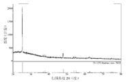
- FIG. 1 is an X-ray diffraction chart of a transparent conductive film in an embodiment of the present application
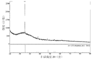
- FIG. 2 is an X-ray diffraction diagram of a transparent conductive film in another embodiment of the present application.
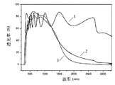
- 3 is a transmission spectrum of a transparent conductive film in another embodiment of the present application, wherein the small image is a physical map;
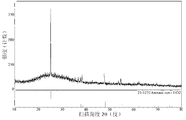
- FIG. 4 is an X-ray diffraction diagram of a transparent conductive film in another embodiment of the present application.
- FIG. 5 is a comparison diagram of ultraviolet-visible-infrared transmission spectra of a transparent conductive film and ITO and FTO in another embodiment of the present application;
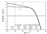
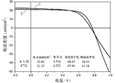
- FIG. 7 is a J-V curve and photoelectric conversion efficiency of a transparent conductive film used as an electrode in a cadmium telluride thin film solar cell according to another embodiment of the present application.
- an antimony-doped titanium dioxide film is prepared by magnetron sputtering, and then treated with barium chloride to obtain an antimony doped and antimony doped titanium dioxide film. details as follows:
- the titanium dioxide powder and the tantalum pentoxide powder are used as the main raw materials, the purity is 4N to 5N, and the molar ratio of Ti:Nb is 9:1, and after mixing, it is ground and uniformly mixed. Then, it was pre-fired at 820 ° C for 3 h in a high-temperature silicon molybdenum furnace; after completion, 5 mL of a polymerization agent polyvinyl alcohol was added, and a circular target having a thickness of 4.5 mm and a diameter of 5 cm was pressed by a powder tableting machine, and then placed in a high-temperature silicon. In the molybdenum furnace, it was sintered at 5 ° C / min to 1350 ° C for 5 h.
- cerium-doped titanium dioxide target was prepared by magnetron sputtering to prepare a cerium-doped titanium dioxide film, wherein the sputtering chamber pressure was 0.3 Pa, the sputtering chamber atmosphere was argon gas, and the substrate was soda-lime-silica glass.
- the substrate temperature was 25 ° C, the sputtering power was 0.5 W/cm 2 , the deposition rate was 10 nm/min, and the sputtering time was 1 h.
- a tantalum-doped titanium dioxide film having a thickness of 600 nm was prepared.
- the transparent conductive film prepared in this example was examined by X-ray diffraction. The results are shown in Fig. 1.
- the crystal form is mainly anatase.
- the doped titanium dioxide with good crystallinity has good preference and large crystal grains.
- the carrier mobility of more than 10 cm 2 /Vs was obtained by the Hall tester, and the carrier concentration was close to 10 20 cm -3 . It can be seen that the transparent conductive film prepared in this example has good conductivity.
- a transmittance of more than 80% was obtained by a transmission spectrometer test.
- the transparent conductive film of this example can achieve the performance indexes of mature products such as ITO, AZO and FTO.
- the transparent conductive film of the present example is a ruthenium and osmium doped titanium dioxide film, which has low raw material cost, abundant resources, and has greater cost and resource advantages, and the preparation method of the present example is simple and easy to operate, and the production cost is low. Suitable for large-scale production.
- an antimony-doped titanium dioxide film is prepared by magnetron sputtering, and then treated with barium chloride to obtain an antimony doped and antimony doped titanium dioxide film. details as follows:
- the ruthenium-doped titania target was prepared in the same manner as in Example 1 using a tantalum pentoxide having a purity of 4N to 5N and a Ti:Ta molar ratio of 19:1.
- the erbium-doped TiO2 film was prepared by magnetron sputtering on the yttrium-doped TiO2 target.
- the magnetron sputtering conditions were as follows: the sputtering chamber pressure was 1.0 Pa, the sputtering chamber atmosphere was argon, and the substrate was A soda-lime-silica glass having a substrate temperature of 50 ° C, a sputtering power of 0.3 W/cm 2 , a deposition rate of 8 nm/min, and a sputtering time of 1 h was prepared to have a thickness of 400 nm.
- cerium-doped titanium dioxide film is treated with cerium chloride, and the cerium-doped titanium dioxide film is immersed in a cerium chloride solution at 60 ° C for 10 minutes, then taken out and heated to 500 ° C under an inert atmosphere, kept for 30 minutes, and cooled. At room temperature, an antimony doped and antimony doped titanium dioxide film, that is, a transparent conductive film of this example, was obtained.
- the transparent conductive film prepared in this example was examined by the same method as in Example 1. The results are shown in Fig. 2, which shows that the crystal form is mainly anatase by X-ray diffraction.
- the Hall tester obtains a carrier mobility of more than 10 cm 2 /Vs, a carrier concentration of approximately 10 20 cm -3 , and a sheet resistance of 10 to 100 ⁇ /sq, and the transparent conductive film has good conductivity.
- the light transmittance in the visible light range is as high as 80%, as shown in FIG. 3, and FIG. 3 respectively shows the light transmittance of the transparent conductive film which is annealed and not annealed, and is not annealed after being immersed in cesium chloride.
- curve 1 is the transmittance of the annealed transparent conductive film
- curve 2 is the transmittance of the transparent conductive film which has not been annealed, and it can be seen that after annealing
- the transparent conductive film of this example has a markedly improved light transmittance.
- the transparent conductive film of this example has the same performance as the transparent conductive film of the first embodiment, and can reach a mature product on the market.
- the transparent conductive film of the present example is a ruthenium and osmium doped titanium dioxide film, which has low raw material cost, abundant resources, greater cost and resource advantages, simple and easy to operate, low production cost, and is more suitable for large Scale production.
- yttrium and lanthanum-doped titanium dioxide films were prepared by magnetron sputtering, and then lanthanum chloride treatment was carried out to obtain yttrium-doped, ytterbium-doped and ytterbium-doped TiO 2 films. details as follows:
- the tantalum source of this example is tantalum pentoxide
- the tantalum source is tantalum pentoxide
- the purity is 4N to 5N
- the molar ratio of Ti:Nb:Ta is 18:1:1, which is the same as that of the first embodiment.
- the yttrium-doped titania target was then subjected to magnetron sputtering to prepare a yttrium-doped titanium dioxide film.
- the magnetron sputtering conditions were as follows: the sputtering chamber pressure was 1.0 Pa, and the sputtering chamber atmosphere was argon.
- the bottom is soda-lime-silica glass
- the substrate temperature is 200 ° C
- the sputtering power is 0.3 W/cm 2
- the deposition rate is 8 nm/min
- the sputtering time is 1 h
- a ruthenium and osmium-doped titanium dioxide film having a thickness of 400 nm is prepared.
- (3) The obtained ruthenium and osmium-doped titanium dioxide film is treated with ruthenium chloride, and the ruthenium-doped titanium dioxide film is immersed in a ruthenium chloride solution at 40 ° C for 60 minutes, and then taken out and heated to 500 ° C under an inert atmosphere for 30 minutes. After cooling to room temperature, a ruthenium-doped, ruthenium and osmium-doped titanium dioxide film, that is, a transparent conductive film of this example, was obtained.
- the transparent conductive film prepared in this example was examined by the same method as in Example 1. The results showed that the crystal form was mainly anatase by X-ray diffraction.
- the Hall tester obtained a carrier mobility of more than 10 cm 2 /Vs, a carrier concentration of approximately 10 20 cm -3 , and a sheet resistance of 100 to 300 ⁇ /sq, and the transparent conductive film was excellent in electrical conductivity.
- the light transmittance in the visible light range is as high as 80%.
- the transparent conductive film of this example has the same performance as the transparent conductive film of the first embodiment, and can reach a mature product on the market.
- the transparent conductive film of the present example is a titanium dioxide film doped with lanthanum, cerium and lanthanum.
- the raw material is low in cost, rich in resources, has greater cost and resource advantages, and the preparation method is simple and easy to operate, and the production cost is low, and is more suitable. For mass production.
- a ruthenium-doped titanium dioxide film is prepared by a solution coating method, and then subjected to ruthenium chloride treatment to obtain a ruthenium-doped and ruthenium-doped titanium oxide film. details as follows:
- coating liquid the pure reagent is analyzed by using n-butyl titanate as the source of titanium, and antimony pentachloride is used as the source of niobium.
- n-butyl titanate As the source of titanium
- antimony pentachloride is used as the source of niobium.
- the molar ratio of titanium source and niobium source 90:10, that is, tetrabutyl titanate 1.531g, 0.135g of antimony pentachloride, added to the ethanol solution, stirred evenly, heated at 80 ° C in air atmosphere, stirred for 1h, prepared a colored gel, concentrated on the gel, and transferred to water heat
- the product powder was centrifuged, and the product powder was redispersed into ethanol to obtain a coating liquid B.
- the conductivity and light transmittance of the transparent conductive film of this example were tested.
- the results show that the transparent conductive film of this example has a transmittance of 75% in the visible light range, a sheet resistance of 100 to 500 ⁇ /sq, and X-ray diffraction test.
- the crystal form is mainly anatase, as shown in Figure 4. It can be seen that the transparent conductive film of this example also has good photoelectric properties.
- a ruthenium-doped titanium dioxide film is prepared by a solution coating method, and then subjected to ruthenium chloride treatment to obtain a ruthenium-doped and ruthenium-doped titanium oxide film. details as follows:
- coating liquid the pure reagent of isopropyl titanate is used as the source of titanium, and the antimony pentachloride is used as the source of lanthanum.
- the molar ratio of titanium source and lanthanum source 95:5, that is, tetrabutyl titanate 1.35g, bismuth pentachloride is 0.068g, added to the ethanol solution, stirred evenly, heated at 80 ° C in air atmosphere, stirred for 1h, to prepare a colored gel, diluted with ethanol to obtain a coating Liquid coating.
- the conductivity and light transmittance of the transparent conductive film of this example were tested.
- the results show that the transparent conductive film of this example has a transmittance of 75% in the visible light range, a sheet resistance of 100 to 500 ⁇ /sq, and X-ray diffraction test.
- the crystal form is mainly anatase. It can be seen that the transparent conductive film of this example also has good photoelectric properties.
- a tantalum and niobium doped titanium dioxide film was prepared by a solution coating method. Details as follows:
- coating liquid the pure reagent is analyzed by tetraethyl titanate as the source of titanium, antimony pentachloride is used as the source of antimony, and barium chloride is used as the source of antimony.
- antimony pentachloride and antimony chloride The molar ratio of 96:4, that is, tetraethyl titanate is 1.095g, ruthenium pentachloride is 0.041g, ruthenium chloride is 0.010g, added to the ethanol solution, stirred uniformly, heated at 80 ° C under argon atmosphere, stirred After 1 h, the temperature was further raised to 120 ° C, and stirred for 1 h to prepare a dark brown solution A, which was diluted with ethanol to prepare a coating liquid.
- the conductivity and light transmittance of the transparent conductive film of this example were tested.
- the results show that the transparent conductive film of this example has a transmittance of 75% in the visible light range, a sheet resistance of 100 to 500 ⁇ /sq, and X-ray diffraction test.
- the crystal form is mainly anatase. It can be seen that the transparent conductive film of this example also has good photoelectric properties.
- a ruthenium and osmium-doped titanium dioxide film is prepared by a solution coating method, and then subjected to ruthenium chloride treatment to obtain a ruthenium-doped, ruthenium- and osmium-doped titanium oxide film. details as follows:
- coating liquid the pure reagent is analyzed by tetraethyl titanate as the source of titanium, antimony pentachloride is used as the source of antimony, and barium chloride is used as the source of antimony.
- antimony pentachloride and antimony chloride The molar ratio of 97:3, that is, tetraethyl titanate is g, ruthenium pentachloride is 0.027 g, and ruthenium chloride is 0.018 g, added to an ethanol solution, stirred uniformly, heated at 80 ° C in an air atmosphere, and stirred for 1 h.
- the soaked film was heated to 350 ° C under a nitrogen atmosphere, kept for 1 h, and cooled to room temperature to obtain a 600 nm thick antimony doped, lanthanum and cerium doped titanium dioxide film, that is, the transparent conductive film of this example.
- the transparent conductive film of this example was tested for conductivity and light transmittance, and the results showed that the transparent conductive film of this example had a transmittance of 75% in the visible light range, a sheet resistance of 100 to 500 ⁇ /sq, and X.
- the crystal form of the diffraction test is mainly anatase. It can be seen that the transparent conductive film of this example also has good photoelectric properties.
- the yttrium-doped titanium dioxide film was prepared by magnetron sputtering in the same manner as in the first embodiment, and then subjected to lanthanum chloride treatment to obtain yttrium-doped and yttrium-doped TiO 2 films.
- the transparent conductive film prepared in this example was tested. The results showed that the crystal form was mainly anatase by X-ray diffraction.
- the Hall tester has a carrier mobility of 3-10 cm 2 /Vs, a carrier concentration of 10 21 cm -3 , and a sheet resistance of 5 to 20 ⁇ /sq, and the transparent conductive film has good conductivity.
- the transparent conductive film prepared in this example was subjected to ultraviolet-visible-infrared transmittance test, and the conventional ITO and FTO were used for comparison test.
- the results show that the transparent conductive film of this example has a transmittance of 70-80% in the ultraviolet-visible-infrared range, as shown in Fig. 5, especially at a transmittance of 1200 nm or more, while the conventional ITO or FTO is 1200 nm.
- the light transmittance of the light wave is significantly reduced. It can be seen that the transparent conductive film of this example has excellent performance in the electrode application of the infrared device.
- curve 1 is a light transmittance test curve of the transparent conductive film of the present example
- curve 2 is a test curve of ITO
- curve 3 is a test curve of FTO.
- the yttrium-doped titanium dioxide film was prepared by magnetron sputtering in the same manner as in the first embodiment, and then subjected to lanthanum chloride treatment to obtain an yttrium-doped and yttrium-doped TiO 2 film. .
- the transparent conductive film prepared in this example was tested. The results showed that the crystal form was mainly anatase by X-ray diffraction.
- the Hall tester has a carrier mobility of 3-10 cm 2 /Vs, a carrier concentration of 10 21 cm -3 , and a sheet resistance of 10 to 20 ⁇ /sq, and the transparent conductive film has good conductivity.
- the light transmittance in the visible light range is as high as 80%.
- ZnO about 30 nm
- P3HT PCBM
- MoO3 about 5-10 nm
- Ag about 150 nm
- the titanium dioxide powder and the tantalum pentoxide powder are used as the main raw materials, the purity is 4N to 5N, and the molar ratio of Ti:Nb is 19:1, and after mixing, it is ground and uniformly mixed. Then, it was pre-fired at 820 ° C for 3 h in a high-temperature silicon molybdenum furnace; after completion, 5 mL of a polymerization agent polyvinyl alcohol was added, and a circular target having a thickness of 4.5 mm and a diameter of 5 cm was pressed by a powder tableting machine, and then placed in a high-temperature silicon. In the molybdenum furnace, it was sintered at 5 ° C / min to 1350 ° C for 5 h.
- cerium-doped titanium dioxide target was prepared by magnetron sputtering to prepare a cerium-doped titanium dioxide film, wherein the sputtering chamber pressure was 0.3 Pa, the sputtering chamber atmosphere was argon gas, and the substrate was soda-lime-silica glass.
- a ruthenium-doped titanium dioxide film having a thickness of 360 nm was prepared at a substrate temperature of 25 ° C, a sputtering power of 0.5 W/cm 2 , a deposition rate of 4 nm/min, and a sputtering time of 1.5 h.
- the obtained solar cell was tested in an AM 1.5G environment (100 mW cm -2 ), and the results are shown in Fig. 6.
- curve 1 is a test curve using the transparent conductive film of the present application
- curve 2 is a test using ITO. curve.
- the open circuit voltage of the obtained battery was 0.557 V
- the short circuit current was 8.21 mA/cm 2
- the filling factor was 49.73%
- the photoelectric conversion efficiency was 2.27%.
- the comparative sample was made of ITO as the conductive film, and the open circuit voltage of the battery was 0.572 V
- the short circuit current was 6.42 mA/cm 2
- the filling factor was 63.89%
- the photoelectric conversion efficiency was 2.35%. It can be seen that the transparent conductive film of this example has excellent performance in optoelectronic device applications.
- the yttrium-doped titanium dioxide film was prepared by magnetron sputtering in the same manner as in the first embodiment, and then lanthanum chloride was treated to obtain yttrium doping and ytterbium doping. Titanium dioxide film.
- the transparent conductive film prepared in this example was tested. The results showed that the crystal form was mainly anatase by X-ray diffraction.
- the Hall tester has a carrier mobility of 3-10 cm 2 /Vs, a carrier concentration of 10 21 cm -3 , and a sheet resistance of 10 to 20 ⁇ /sq, and the transparent conductive film has good conductivity.
- the light transmittance in the visible light range is as high as 80%.
- CdS about 150 nm
- CdTe 4-5 ⁇ m
- Cu about 1-5 nm
- Au about 80 nm
- the titanium dioxide powder and the tantalum pentoxide powder are used as the main raw materials, the purity is 4N to 5N, and the molar ratio of Ti:Ta is 19:1, and after mixing, it is ground and uniformly mixed. Then, it was pre-fired at 820 ° C for 3 h in a high-temperature silicon molybdenum furnace; after completion, 5 mL of a polymerization agent polyvinyl alcohol was added, and a circular target having a thickness of 4.5 mm and a diameter of 5 cm was pressed by a powder tableting machine, and then placed in a high-temperature silicon. In the molybdenum furnace, it was sintered at 5 ° C / min to 1350 ° C for 5 h.
- cerium-doped titanium dioxide target was prepared by magnetron sputtering to prepare a cerium-doped titanium dioxide film, wherein the sputtering chamber pressure was 0.3 Pa, the sputtering chamber atmosphere was argon gas, and the substrate was soda-lime-silica glass.
- a ruthenium-doped titanium dioxide film having a thickness of 360 nm was prepared at a substrate temperature of 25 ° C, a sputtering power of 0.5 W/cm 2 , a deposition rate of 4 nm/min, and a sputtering time of 1.5 h.
- curve 1 is a test curve using the transparent conductive film of the present application
- curve 2 is a test using FTO. curve.
- the open circuit voltage of the battery was 0.753 V
- the short circuit current was 22.64 mA/cm 2
- the fill factor was 60.65%
- the photoelectric conversion efficiency was 10.34%
- the comparative sample was made of FTO as the conductive film, and the open circuit voltage of the battery was 0.772V, the short circuit current was 21.33 mA/cm 2 , the filling factor was 67.90%, and the photoelectric conversion efficiency was 11.18%. It can be seen that the transparent conductive film of this example has excellent performance in optoelectronic device applications.
Landscapes
- Chemical & Material Sciences (AREA)
- Chemical Kinetics & Catalysis (AREA)
- Engineering & Computer Science (AREA)
- Materials Engineering (AREA)
- Mechanical Engineering (AREA)
- Metallurgy (AREA)
- Organic Chemistry (AREA)
- Non-Insulated Conductors (AREA)
- Inorganic Compounds Of Heavy Metals (AREA)
Abstract
本申请公开了一种掺杂二氧化钛透明导电薄膜及其制备方法和应用。本申请的透明导电薄膜为掺杂二氧化钛薄膜,其中,掺杂为钌掺杂,以及铌和/或钽掺杂。本申请的透明导电薄膜,在二氧化钛中掺杂钌,同时掺杂铌和钽中的一种或两种,使得制备的掺杂二氧化钛薄膜,导电性能优良,耐温性好,透光率高;并且,本申请的透明导电薄膜其原材料成本低廉资源丰富,其制备方法也简单易操作,能够满足大规模批量生产的需求,为透明导电薄膜的推广应用和研究奠定了基础。
Description
本申请涉及透明导电薄膜领域,特别是涉及一种透明导电薄膜及其制备方法和应用。
随着世界范围内柔性显示产业的迅猛发展,大面积的透明导电氧化物(缩写TCO)玻璃基板的需求将长时间保持迅猛增长。据初步测算,到2020年世界范围内TCO玻璃基板的需求量将超过12亿平方米。现有产业界广泛应用的透明导电膜主要包括氧化铟锡(缩写ITO),氧化锌铝(缩写AZO)和氟掺杂氧化锡(缩写FTO)三大类。其中ITO因大量使用昂贵的铟材料,使其应用受到极大限制。FTO和AZO体系的光电性能接近ITO水平,在平板显示器中得到部分应用,但是FTO和AZO的制备过程中需要引入高温工艺,对生产条件要求比较高,因此对FTO和AZO的广泛应用造成了限制。
为了进一步降低成本,避免使用稀有金属铟,且不降低导电薄膜的性能,使TCO在生产中更具竞争优势,则需要把透明导电薄膜的材料作为关键问题来解决。二氧化钛基薄膜以其优异的光电性能及价廉且资源丰富而在光催化等应用上已经获得广泛的应用,但是,作为导电薄膜时,其导电性和透光性较差,无法取得良好的效果。
发明内容
本申请的目的是提供一种改进的新的透明导电薄膜及其制备方法和应用。
本申请采用了以下技术方案:
本申请的一方面公开了一种透明导电薄膜,该透明导电薄膜为掺杂二氧化钛薄膜,其中,掺杂为钌掺杂,以及铌和/或钽掺杂。
需要说明的是,本申请的关键在于创造性的在二氧化钛中进行钌掺杂,与此同时,将铌和钽中的一种或两种掺杂到二氧化碳中;使得制备的掺杂二氧化钛薄膜,在作为透明导电薄膜使用时,具备良好的导电性和透光性,其性能与目前主流的ITO、FTO和AZO相当,但是,掺杂二氧化钛其原材料成本和生产成本低很多,其制备方法简单易操作,能够满足大规模批量化生产的需求。本申请的透明导电薄膜,其导电性提高两倍以上,透光性提升10%;在还原气氛和等离子气氛下有很高的耐温性,其稳定性远高于ITO、AZO;避免了使用F
源这一有毒物质;并且,在紫外-可见-红外光谱有很高的透过率,特别适合薄膜太阳能电池器件、平面显示器件、触摸屏器件及制备红外器件使用。
可以理解,本申请的关键在于创造性的发现,在二氧化钛薄膜中掺杂钌,以及铌和钽中的一种或两种,能够获得性能良好的透明导电薄膜;至于钌,铌和/或钽的具体掺杂量,可以根据不同的生产需求或产品需求而定,在此不做具体限定。但是,本申请优选的方案中,为了保障获得性能更稳定、良好的透明导电薄膜,对钌,铌和/或钽的掺杂量进行了特别限定,详细方案将在下文介绍。
优选的,钌掺杂的量为总重量的0.1-5%,铌掺杂的量为总重量的0.1-20%,钽掺杂的量为总重量的0.1-20%。
优选的,二氧化钛的晶相为锐钛矿相。
本申请的另一面还公开了本申请的透明导电薄膜在显示屏、触摸屏、光伏器件或光电子器件中的应用。
可以理解,本申请的透明导电薄膜,其原材料二氧化钛、钌、铌、钽都是廉价且资源丰富的原材料,并且,其性能也与目前主流的ITO、FTO和AZO相当,因此,在没有成本顾虑的情况下,可以替换ITO、FTO和AZO的应用;尤其是在显示屏、触摸屏或光电子器件中的应用。
本申请的另一面还公开了一种透明导电玻璃,包括衬底和导电薄膜,其导电薄膜为本申请的透明导电薄膜,衬底为玻璃、石英、蓝宝石和有机薄膜中的至少一种。
本申请的另一面还公开了一种含有本申请的透明导电薄膜的复合电极。
本申请的另一面还公开了本申请的透明导电薄膜的一种制备方法,包括采用磁控溅射法制备铌和/或钽掺杂二氧化钛膜,然后对铌和/或钽掺杂二氧化钛膜进行钌化合物处理;磁控溅射法包括,将铌源粉末和/或钽源粉末,与二氧化钛粉末按化学计量比混合,研磨均匀,然后高温煅烧压制成掺杂二氧化钛靶材,采用磁控溅射制成铌和/或钽掺杂二氧化钛膜;钌化合物处理包括,将铌和/或钽掺杂二氧化钛膜浸泡到钌化合物溶液中,在10~150℃反应10~120min,然后将铌和/或钽掺杂二氧化钛膜置于真空或惰性气氛或还原气氛中,在100~650℃保温0-10h,冷却到室温,即获得钌掺杂,以及铌和/或钽掺杂,的二氧化钛薄膜。
需要说明的是,本申请的磁控溅射法是在真空下进行的,因此又称为真空制备掺杂二氧化钛薄膜。其中,靶材的制备可以参照一般的磁控溅射靶材的制备,在此不累述;至于靶材中铌源粉末、钽源粉末,二氧化钛粉末的用量,可以根据不同的生产需求和产品需求进行调控,在此不累述。“和/或”的意思是,可以是铌掺杂和钽掺杂一起,也可以是铌掺杂或者钽掺杂。磁控溅射的具体条
件也可以参考常规的磁控溅射方法,根据所需要的铌和/或钽掺杂二氧化钛膜的厚度而定,在本申请的优选方案中,对磁控溅射条件进行了特别限定。此外,钌化合物溶液的浓度,以及具体处理时间和温度等,可以根据需要的钌掺杂量进行调控;可以理解,如果需要掺杂的钌量越大,则在化学剂量允许的条件下,可以采用更高浓度的钌化合物,处理时间长些、温度高些,反之则反;在此不做具体限定。
优选的,钌化合物为卤素钌、氧化钌、钌盐和钌有机化合物中的至少一种。
优选的,铌源粉末为纳米铌粉和/或五氧化二铌;所述钽源粉末为纳米钽粉和/或五氧化二钽。
优选的,磁控溅射制成所述铌和/或钽掺杂二氧化钛膜的具体条件为,溅射腔压强0.1~10Pa,溅射腔气氛为氩气或氮气或氩氢混合气,衬底为玻璃、石英片、蓝宝石或有机衬底,衬底温度为10~500℃,溅射功率为0.01~10W/cm2,沉积速率为0.1~500nm/min,溅射时间为0.01~5h。
本申请的另一面还公开了本申请的透明导电薄膜的另一种制备方法,包括将铌源和/或钽源,与钌源和钛源一起按化学计量比分散到溶剂中,在空气或惰性气氛下进行热反应,将反应产物涂覆在基底上,烘干溶剂,即获得钌掺杂,以及铌和/或钽掺杂,的二氧化钛薄膜。
需要说明的是,本申请的一种实现方式中,在将反应产物涂覆到基底上之前,根据具体试验需求,还预先对反应产物进行了稀释。在本申请的另外一种实现方式中,在将反应产物涂覆到基底上之前,还对反应产物溶液进行了浓缩,然后置于反应釜中高温高压处理,然后离心获取沉底,采用溶剂对沉淀进行分散后作为涂覆液,涂覆到基底上。也就是说,根据不同的生产条件,或具体生产情况,在反应产物涂覆到基底上之前,还可以包含对反应产物溶液进行各种处理的步骤,在此不做具体限定。
本申请的另一面还公开了本申请的透明导电薄膜的再一种制备方法,包括将铌源和/或钽源,与钛源一起按化学计量比分散到溶剂中,在空气或惰性气氛下进行热反应,将反应产物涂覆在基底上,烘干溶剂,即获得铌和/或钽掺杂二氧化钛膜;将铌和/或钽掺杂二氧化钛膜浸泡到钌化合物溶液中,在10~150℃反应10~120min,然后将铌和/或钽掺杂二氧化钛膜置于真空或惰性气氛或还原气氛中,在100~650℃保温0-10h,冷却到室温,即获得钌掺杂,以及铌和/或钽掺杂,的二氧化钛薄膜。
需要说明的是,以上两种制备方法的区别在于,在反应液中是否有加入钌源,如果有加入钌源,则可以直接制备出钌掺杂,以及铌和/或钽掺杂的二氧化
钛薄膜;如果没有加钌源,则需要对制备的铌和/或钽掺杂二氧化钛膜进行钌化合物处理。
优选的,热反应的条件为,在30-300℃下反应0.1-6h。
优选的,铌源为氯化铌、乙醇铌、纳米铌粉和五氧化二铌中的至少一种;钽源为氯化钽、乙醇钽、纳米钽粉、五氧化二钽和甲醇钽中的至少一种;钛源为钛酸正丁酯、钛酸异丙酯和钛酸四乙酯中的至少一种。
优选的,溶剂为蒸馏水、乙醇、正丁醇、乙腈、甲醇、2-甲氧基乙醇、异丙醇、乙二醇、N,N-二甲基甲酰胺和四氢呋喃中的至少一种。
优选的,钌化合物为卤素钌,氧化钌,钌盐和钌有机化合物中的至少一种。
本申请的有益效果在于:
本申请的透明导电薄膜,在二氧化钛中掺杂钌,同时掺杂铌和钽中的一种或两种,使得制备的掺杂二氧化钛薄膜,导电性能优良,耐温性好,透光率高;并且,本申请的透明导电薄膜其原材料成本低廉资源丰富,其制备方法也简单易操作,能够满足大规模批量生产的需求,为透明导电薄膜的推广应用和研究奠定了基础。
图1是本申请实施例中透明导电薄膜的X射线衍射图;
图2是本申请另一实施例中透明导电薄膜的X射线衍射图;
图3是本申请另一实施例中透明导电薄膜的透过谱,其中小图是实物图;
图4是本申请另一实施例中透明导电薄膜的X射线衍射图;
图5是本申请另一实施例中透明导电薄膜与ITO及FTO的紫外-可见-红外的透过谱对比图;
图6是本申请另一实施例中透明导电薄膜作为电极在有机薄膜太阳能电池中应用的J-V曲线及光电转换效率;
图7是本申请另一实施例中透明导电薄膜作为电极在碲化镉薄膜太阳能电池中应用的J-V曲线及光电转换效率。
下面通过具体实施例对本申请作进一步详细说明。以下实施例仅对本申请进行进一步说明,不应理解为对本申请的限制。
实施例一
本例的透明导电薄膜,采用磁控溅射法制备铌掺杂二氧化钛膜,然后进行氯化钌处理,获得钌掺杂和铌掺杂的二氧化钛薄膜。具体如下:
(1)以二氧化钛粉和五氧化二铌粉末为主要原料,纯度为4N~5N,按照Ti:Nb摩尔比为9:1配料,混合后经过研磨,使之混合均匀。而后放入高温硅钼炉中在820℃下预烧3h;完成后加入聚合剂聚乙烯醇5mL,用粉末压片机压制成4.5mm厚、直径5cm的圆形靶材,然后放入高温硅钼炉中以5℃/min升至1350℃烧结5h,冷却后,固定0.5mm厚的铜背底,即制得铌掺杂二氧化钛靶材。(2)得到的铌掺杂二氧化钛靶材采用磁控溅射工艺,制备铌掺杂二氧化钛膜,其中溅射腔压强为0.3Pa,溅射腔气氛为氩气,衬底为钠钙硅玻璃,衬底温度为25℃,溅射功率为0.5W/cm2,沉积速率为10nm/min,溅射时间为1h,制备出600nm厚度的铌掺杂二氧化钛膜。(3)铌掺杂二氧化钛膜的氯化钌处理,将铌掺杂二氧化钛膜浸泡在氯化钌溶液中50℃下处理10min,然后取出于惰性气氛下加热至450℃,保温30min,冷却到室温,得到钌掺杂和铌掺杂的二氧化钛薄膜,即本例的透明导电薄膜。
采用X射线衍射对本例制备的透明导电薄膜进行检测,结果如图1所示,本例制备的透明导电薄膜中,其晶型主要为锐钛矿。结晶性良好的掺杂二氧化钛择优性能好,晶粒大。通过霍尔测试仪获得大于10cm2/Vs的载流子迁移率,载流子浓度接近1020cm-3,可见本例制备的透明导电薄膜导电性良好。另外,通过透射光谱仪测试,获得大于80%的透光率。
以上测试结果显示,本例的透明导电薄膜,能够达到市面成熟产品,如ITO、AZO和FTO的性能指标。但是,本例的透明导电薄膜为钌和铌掺杂的二氧化钛薄膜,其原材料成本低廉资源丰富,具有更大的成本和资源优势,并且,本例的制备方法简单易操作,生产成本低,更适合于大规模生产。
实施例二
本例的透明导电薄膜,采用磁控溅射法制备钽掺杂二氧化钛膜,然后进行氯化钌处理,获得钌掺杂和钽掺杂的二氧化钛薄膜。具体如下:
(1)本例的钽源采用五氧化二钽,纯度为4N~5N,按照Ti:Ta摩尔比为19:1配料,采用与实施例一相同的方法制备钽掺杂二氧化钛靶材。(2)然后对钽掺杂二氧化钛靶材进行磁控溅射,制备钽掺杂二氧化钛膜,磁控溅射条件为:溅射腔压强为1.0Pa,溅射腔气氛为氩气,衬底为钠钙硅玻璃,衬底温度为50℃,溅射功率为0.3W/cm2,沉积速率为8nm/min,溅射时间为1h,制备出400nm厚度的钽掺杂二氧化钛膜。(3)得到的钽掺杂二氧化钛膜进行氯化钌处理,将
钽掺杂二氧化钛膜浸泡在氯化钌溶液中60℃下处理10min,然后取出于惰性气氛下加热至500℃,保温30min,冷却到室温,得到钌掺杂和钽掺杂的二氧化钛薄膜,即本例的透明导电薄膜。
采用实施例一相同的方法,对本例制备的透明导电薄膜进行检测。结果如图2所示,显示X射线衍射测定其晶型主要为锐钛矿。霍尔测试仪获得大于10cm2/Vs的载流子迁移率,载流子浓度接近1020cm-3,并且,方块电阻10~100Ω/sq,透明导电薄膜导电性良好。此外,可见光范围内透光率高达80%,如图3所示,图3分别显示了经退火处理和没有经退火处理的透明导电薄膜的透光率,没有经退火处理即氯化钌浸泡后不进行惰性气氛500℃加热保温30min;图中,曲线1为经过退火处理的透明导电薄膜的透光率,曲线2为没有经过退火处理的透明导电薄膜的透光率,可见,经过退火处理后的本例的透明导电薄膜,其透光率明显提高。
可见,本例的透明导电薄膜,与实施例一的透明导电薄膜性能相当,能够达到市面成熟产品。并且,同样的,本例的透明导电薄膜为钌和钽掺杂的二氧化钛薄膜,原材料成本低廉资源丰富,具有更大的成本和资源优势,制备方法简单易操作,生产成本低,更适合于大规模生产。
实施例三
本例的透明导电薄膜,采用磁控溅射法制备铌和钽掺杂二氧化钛膜,然后进行氯化钌处理,获得钌掺杂、铌掺杂和钽掺杂的二氧化钛薄膜。具体如下:
(1)本例的铌源采用五氧化二铌,钽源采用五氧化二钽,纯度为4N~5N,按照Ti:Nb:Ta摩尔比为18:1:1配料,采用与实施例一相同的方法制备铌和钽掺杂二氧化钛靶材。(2)然后对铌和钽掺杂二氧化钛靶材进行磁控溅射,制备钽掺杂二氧化钛膜,磁控溅射条件为:溅射腔压强为1.0Pa,溅射腔气氛为氩气,衬底为钠钙硅玻璃,衬底温度为200℃,溅射功率为0.3W/cm2,沉积速率为8nm/min,溅射时间为1h,制备出400nm厚度的铌和钽掺杂二氧化钛膜。(3)得到的铌和钽掺杂二氧化钛膜进行氯化钌处理,将铌掺杂二氧化钛膜浸泡在氯化钌溶液中40℃下处理60min,然后取出于惰性气氛下加热至500℃,保温30min,冷却到室温,得到钌掺杂、铌和钽掺杂的二氧化钛薄膜,即本例的透明导电薄膜。
采用实施例一相同的方法,对本例制备的透明导电薄膜进行检测。结果显示,X射线衍射测定其晶型主要为锐钛矿。霍尔测试仪获得大于10cm2/Vs的载流子迁移率,载流子浓度接近1020cm-3,并且,方块电阻100~300Ω/sq,透明导
电薄膜导电性良好。此外,可见光范围内透光率高达80%。
可见,本例的透明导电薄膜,与实施例一的透明导电薄膜性能相当,能够达到市面成熟产品。并且,同样的,本例的透明导电薄膜为钌、铌和钽掺杂的二氧化钛薄膜,原材料成本低廉资源丰富,具有更大的成本和资源优势,制备方法简单易操作,生产成本低,更适合于大规模生产。
实施例四
本例的透明导电薄膜,采用溶液涂覆法制备铌掺杂二氧化钛膜,然后进行氯化钌处理,获得钌掺杂和铌掺杂的二氧化钛薄膜。具体如下:
(1)涂覆液的制备:以钛酸正丁酯分析纯试剂为钛源,五氯化铌为铌源,按照钛源和铌源的摩尔比例90:10,即钛酸四丁酯为1.531g,五氯化铌为0.135g,加入到乙醇溶液中,搅拌均匀,在空气气氛下加热80℃,搅拌1h,制备得到有颜色的凝胶,对凝胶进行浓缩,并转移到水热釜中,进行210℃处理4h后,离心得到产物粉体,将产物粉末重新分散到乙醇中获得涂覆液B。(2)成膜:将涂覆液B刮涂在白玻璃基底上,然后在120℃下烘干溶剂,得到铌掺杂二氧化钛膜。(3)氯化钌处理:对步骤(2)的铌掺杂二氧化钛膜进行表面清理,本例采用UV辐照30min进行表面清理,然后置于氯化钌溶液中70℃浸泡15min,取出浸泡后的薄膜,在氮气气氛下加热至450℃,保温0.5h,冷却到室温,即得到800nm厚的钌掺杂和铌掺杂二氧化钛薄膜,即本例的透明导电薄膜。
对本例的透明导电薄膜进行导电性和透光性测试,结果显示,本例的透明导电薄膜,其可见光范围内透过率为75%,方块电阻100~500Ω/sq,并且,X衍射测试其晶型主要为锐钛矿,如图4所示。可见,本例的透明导电薄膜,同样具有良好的光电性能。
实施例五
本例的透明导电薄膜,采用溶液涂覆法制备铌掺杂二氧化钛膜,然后进行氯化钌处理,获得钌掺杂和铌掺杂的二氧化钛薄膜。具体如下:
(1)涂覆液的制备:以钛酸异丙酯分析纯试剂为钛源,五氯化铌为铌源,按照钛源和铌源的摩尔比例95:5,即钛酸四丁酯为1.35g,五氯化铌为0.068g,加入到乙醇溶液中,搅拌均匀,在空气气氛下加热80℃,搅拌1h,制备得到有颜色的凝胶,采用乙醇对凝胶进行稀释,即获得涂覆液。(2)成膜:将涂覆液旋涂在白玻璃基底上,旋涂方式为1.5k rpm,涂5次,然后在120℃下烘干溶剂,得到铌掺杂二氧化钛膜。(3)氯化钌处理:对步骤(2)的铌掺杂二氧化钛膜进
行表面清理,本例采用UV辐照30min进行表面清理,然后置于氯化钌溶液中70℃浸泡15min,取出浸泡后的薄膜,在氮气气氛下加热至450℃,保温0.5h,冷却到室温,即得到500nm厚的钌掺杂和铌掺杂二氧化钛薄膜,即本例的透明导电薄膜。
对本例的透明导电薄膜进行导电性和透光性测试,结果显示,本例的透明导电薄膜,其可见光范围内透过率为75%,方块电阻100~500Ω/sq,并且,X衍射测试其晶型主要为锐钛矿。可见,本例的透明导电薄膜,同样具有良好的光电性能。
实施例六
本例的透明导电薄膜,采用溶液涂覆法制备钌和铌掺杂二氧化钛薄膜。具体如下:
(1)涂覆液的制备:以钛酸四乙酯分析纯试剂为钛源,五氯化铌为铌源,氯化钌为钌源,按照钛源:五氯化铌和氯化钌的摩尔比例96:4,即钛酸四乙酯为1.095g,五氯化铌为0.041g,氯化钌为0.010g,加入到乙醇溶液中,搅拌均匀,在氩气气氛下加热80℃,搅拌1h,再升温至120℃,搅拌1h,制备得到深棕色的溶液A,采用乙醇对溶液A进行稀释,制备成涂覆液。(2)成膜:将涂覆液旋涂在白玻璃基底上,旋涂方式为1.5k rpm,涂2次,然后在120℃下烘干溶剂,冷却到室温,即得到450nm厚的钌掺杂和铌掺杂二氧化钛薄膜,即本例的透明导电薄膜。
对本例的透明导电薄膜进行导电性和透光性测试,结果显示,本例的透明导电薄膜,其可见光范围内透过率为75%,方块电阻100~500Ω/sq,并且,X衍射测试其晶型主要为锐钛矿。可见,本例的透明导电薄膜,同样具有良好的光电性能。
实施例七
本例的透明导电薄膜,采用溶液涂覆法制备铌和钽掺杂二氧化钛膜,然后进行氯化钌处理,获得钌掺杂、铌和钽掺杂的二氧化钛薄膜。具体如下:
(1)涂覆液的制备:以钛酸四乙酯分析纯试剂为钛源,五氯化铌为铌源,氯化钽为钽源,按照钛源:五氯化铌和氯化钽的摩尔比例97:3,即钛酸四乙酯为g,五氯化铌为0.027g,氯化钽为0.018g,加入到乙醇溶液中,搅拌均匀,在空气气氛下加热80℃,搅拌1h,再升温至120℃,搅拌1h,制备得到深棕色的溶液A,对溶液A进行稀释,制备成涂覆液。(2)成膜:将涂覆液喷涂到白
玻璃基底上,喷雾喷涂20min,基底的温度保持为120℃,喷雾喷涂完成后直接获得铌和钽掺杂二氧化钛膜。(3)氯化钌处理:对步骤(2)的铌和钽掺杂二氧化钛膜进行表面清理,本例采用UV辐照5min进行表面清理,然后置于氯化钌溶液中70℃浸泡15min,取出浸泡后的薄膜,在氮气气氛下加热至350℃,保温1h,冷却到室温,即得到600nm厚的钌掺杂、铌和钽掺杂二氧化钛薄膜,即本例的透明导电薄膜。
同样的,对本例的透明导电薄膜进行导电性和透光性测试,结果显示,本例的透明导电薄膜,其可见光范围内透过率为75%,方块电阻100~500Ω/sq,并且,X衍射测试其晶型主要为锐钛矿。可见,本例的透明导电薄膜,同样具有良好的光电性能。
实施例八
本例采用实施例一相同的方法,通过磁控溅射法制备铌掺杂二氧化钛膜,然后进行氯化钌处理,获得钌掺杂和铌掺杂的二氧化钛薄膜。对本例制备的透明导电薄膜进行检测。结果显示,X射线衍射测定其晶型主要为锐钛矿。霍尔测试仪获得3-10cm2/Vs的载流子迁移率,载流子浓度在1021cm-3量级,并且,方块电阻5~20Ω/sq,透明导电薄膜导电性良好。
此外,对本例制备的透明导电薄膜进行紫外-可见-红外透光率测试,并采用传统的ITO和FTO作对比测试。结果显示,本例的透明导电薄膜紫外-可见-红外范围内透光率高达70-80%,如图5所示,特别是在1200nm以上的透光率良好,而传统的ITO或FTO对1200nm光波的透光率明显锐减。可见,本例的透明导电薄膜,在红外器件的电极应用上具有优异的性能。图5中,曲线1为本例的透明导电薄膜的透光率测试曲线,曲线2为ITO的测试曲线,曲线3为FTO的测试曲线。
实施例九
本例有机太阳能电池中的透明导电薄膜,采用实施例一相同的方法,通过磁控溅射法制备铌掺杂二氧化钛膜,然后进行氯化钌处理,获得钌掺杂和铌掺杂的二氧化钛薄膜。对本例制备的透明导电薄膜进行检测。结果显示,X射线衍射测定其晶型主要为锐钛矿。霍尔测试仪获得3-10cm2/Vs的载流子迁移率,载流子浓度在1021cm-3量级,并且,方块电阻10~20Ω/sq,透明导电薄膜导电性良好。此外,可见光范围内透光率高达80%。该导电薄膜经清洗后,依次沉积ZnO(约30nm)、P3HT:PCBM(约200nm)、MoO3(约5-10nm)和Ag
(约150nm)。具体如下:
(1)以二氧化钛粉和五氧化二铌粉末为主要原料,纯度为4N~5N,按照Ti:Nb摩尔比为19:1配料,混合后经过研磨,使之混合均匀。而后放入高温硅钼炉中在820℃下预烧3h;完成后加入聚合剂聚乙烯醇5mL,用粉末压片机压制成4.5mm厚、直径5cm的圆形靶材,然后放入高温硅钼炉中以5℃/min升至1350℃烧结5h,冷却后,固定0.5mm厚的铜背底,即制得铌掺杂二氧化钛靶材。(2)得到的铌掺杂二氧化钛靶材采用磁控溅射工艺,制备铌掺杂二氧化钛膜,其中溅射腔压强为0.3Pa,溅射腔气氛为氩气,衬底为钠钙硅玻璃,衬底温度为25℃,溅射功率为0.5W/cm2,沉积速率为4nm/min,溅射时间为1.5h,制备出360nm厚度的铌掺杂二氧化钛膜。(3)铌掺杂二氧化钛膜的氯化钌处理,将铌掺杂二氧化钛膜浸泡在氯化钌溶液中50℃下处理10min,然后取出于惰性气氛下加热至450℃,保温30min,冷却到室温,得到钌掺杂和铌掺杂的二氧化钛薄膜,即本例的透明导电薄膜。(4)得到的导电膜,经洗涤剂、蒸馏水、丙酮和异丙醇超声清洗后,在80℃下烘干。(5)导电膜表面经UV/臭氧处理后,旋涂ZnO的前驱液,在200℃下处理1h,然后旋涂P3HT:PCBM(1:1),在150℃下烘干溶剂后,蒸镀5nm MoO3,最后蒸镀150nm Ag,得到本例中的有机太阳能电池。
在AM 1.5G环境下(100mW cm-2),对所得的太阳能电池进行测试,结果如图6所示,图中曲线1为采用本申请透明导电薄膜的测试曲线,曲线2为采用ITO的测试曲线。得到电池的开路电压为0.557V,短路电流为8.21mA/cm2,填充因子为49.73%,光电转换效率为2.27%。对比样品以ITO为导电膜,得到电池的开路电压为0.572V,短路电流为6.42mA/cm2,填充因子为63.89%,光电转换效率为2.35%。可见,本例的透明导电薄膜,在光电器件应用中具有优异的性能。
实施例十
本例碲化镉薄膜太阳能电池中的透明导电薄膜,采用实施例一相同的方法,通过磁控溅射法制备钽掺杂二氧化钛膜,然后进行氯化钌处理,获得钌掺杂和钽掺杂的二氧化钛薄膜。对本例制备的透明导电薄膜进行检测。结果显示,X射线衍射测定其晶型主要为锐钛矿。霍尔测试仪获得3-10cm2/Vs的载流子迁移率,载流子浓度在1021cm-3量级,并且,方块电阻10~20Ω/sq,透明导电薄膜导电性良好。此外,可见光范围内透光率高达80%。该导电薄膜经清洗后,依次沉积CdS(约150nm)、CdTe(4-5μm)、Cu(约1-5nm)和Au(约80nm)。
具体如下:
(1)以二氧化钛粉和五氧化二钽粉末为主要原料,纯度为4N~5N,按照Ti:Ta摩尔比为19:1配料,混合后经过研磨,使之混合均匀。而后放入高温硅钼炉中在820℃下预烧3h;完成后加入聚合剂聚乙烯醇5mL,用粉末压片机压制成4.5mm厚、直径5cm的圆形靶材,然后放入高温硅钼炉中以5℃/min升至1350℃烧结5h,冷却后,固定0.5mm厚的铜背底,即制得钽掺杂二氧化钛靶材。(2)得到的钽掺杂二氧化钛靶材采用磁控溅射工艺,制备钽掺杂二氧化钛膜,其中溅射腔压强为0.3Pa,溅射腔气氛为氩气,衬底为钠钙硅玻璃,衬底温度为25℃,溅射功率为0.5W/cm2,沉积速率为4nm/min,溅射时间为1.5h,制备出360nm厚度的钽掺杂二氧化钛膜。(3)钽掺杂二氧化钛膜的氯化钌处理,将钽掺杂二氧化钛膜浸泡在氯化钌溶液中50℃下处理10min,然后取出于惰性气氛下加热至450℃,保温30min,冷却到室温,得到钌掺杂和钽掺杂的二氧化钛薄膜,即本例的透明导电薄膜。(4)得到的导电膜,经洗涤剂、蒸馏水、丙酮和异丙醇超声清洗后,在80℃下烘干。(5)导电膜表面经UV/臭氧处理后,溅射150nm CdS层,然后通过近空间升华法沉积4-5μm CdTe,经CdCl2退火处理和酸刻蚀后,蒸镀1-3nm Cu,最后蒸镀80nm Au,经180℃退火,得到本例中的碲化镉薄膜太阳能电池。
在AM 1.5G环境下(100mW cm-2),对所得的太阳能电池进行测试,结果如图7所示,图中曲线1为采用本申请透明导电薄膜的测试曲线,曲线2为采用FTO的测试曲线。得到电池的开路电压为0.753V,短路电流为22.64mA/cm2,填充因子为60.65%,光电转换效率为10.34%。对比样品以FTO为导电膜,得到电池的开路电压为0.772V,短路电流为21.33mA/cm2,填充因子为67.90%,光电转换效率为11.18%。可见,本例的透明导电薄膜,在光电器件应用中具有优异的性能。
以上内容是结合具体的实施方式对本申请所作的进一步详细说明,不能认定本申请的具体实施只局限于这些说明。对于本申请所属技术领域的普通技术人员来说,在不脱离本申请构思的前提下,还可以做出若干简单推演或替换,都应当视为属于本申请的保护范围。
Claims (10)
- 一种透明导电薄膜,其特征在于:所述透明导电薄膜为掺杂二氧化钛薄膜,所述掺杂为钌掺杂,以及铌和/或钽掺杂。
- 根据权利要求1所述的透明导电薄膜,其特征在于:所述钌掺杂的量为总重量的0.1-5%,铌掺杂的量为总重量的0.1-20%,钽掺杂的量为总重量的0.1-20%。
- 根据权利要求1或2所述的透明导电薄膜,其特征在于:所述二氧化钛的晶相为锐钛矿相。
- 根据权利要求1-3任一项所述的透明导电薄膜在显示屏、触摸屏、光伏器件或光电子器件中的应用。
- 一种透明导电玻璃,包括衬底和导电薄膜,其特征在于:所述导电薄膜为权利要求1-3任一项所述的透明导电薄膜,所述衬底为玻璃、石英、蓝宝石和有机薄膜中的至少一种。
- 一种含有权利要求1-3任一项所述的透明导电薄膜的复合电极。
- 根据权利要求1-3所述的透明导电薄膜的制备方法,其特征在于:包括采用磁控溅射法制备铌和/或钽掺杂二氧化钛膜,然后对铌和/或钽掺杂二氧化钛膜进行钌化合物处理;所述磁控溅射法包括,将铌源粉末和/或钽源粉末,与二氧化钛粉末按化学计量比混合,研磨均匀,然后高温煅烧压制成掺杂二氧化钛靶材,采用磁控溅射制成所述铌和/或钽掺杂二氧化钛膜;所述钌化合物处理包括,将所述铌和/或钽掺杂二氧化钛膜浸泡到钌化合物溶液中,在10~150℃反应10~120min,然后将铌和/或钽掺杂二氧化钛膜置于真空或惰性气氛或还原气氛中,在100~650℃保温0-10h,冷却到室温,即获得钌掺杂,以及铌和/或钽掺杂,的二氧化钛薄膜。
- 根据权利要求1-3任一项所述的透明导电薄膜的制备方法,其特征在于:包括将铌源和/或钽源,与钌源和钛源一起按化学计量比分散到溶剂中,在空气或惰性气氛下进行热反应,将反应产物涂覆在基底上,烘干溶剂,即获得钌掺杂,以及铌和/或钽掺杂,的二氧化钛薄膜。
- 根据权利要求1-3任一项所述的透明导电薄膜的制备方法,其特征在于:包括将铌源和/或钽源,与钛源一起按化学计量比分散到溶剂中,在空气或惰性气氛下进行热反应,将反应产物涂覆在基底上,烘干溶剂,即获得所述铌和/或钽掺杂二氧化钛膜;将所述铌和/或钽掺杂二氧化钛膜浸泡到钌化合物溶液中,在10~150℃反应10~120min,然后将铌和/或钽掺杂二氧化钛膜置于真空或惰性 气氛或还原气氛中,在100~650℃保温0-10h,冷却到室温,即获得钌掺杂,以及铌和/或钽掺杂,的二氧化钛薄膜。
- 根据权利要求8或9所述的制备方法,其特征在于:所述铌源为氯化铌、乙醇铌、纳米铌粉和五氧化二铌中的至少一种;所述钽源为氯化钽、乙醇钽、纳米钽粉、五氧化二钽和甲醇钽中的至少一种;所述钛源为钛酸正丁酯、钛酸异丙酯和钛酸四乙酯中的至少一种;所述溶剂为蒸馏水、乙醇、正丁醇、乙腈、甲醇、2-甲氧基乙醇、异丙醇、乙二醇、N,N-二甲基甲酰胺和四氢呋喃中的至少一种;钌化合物为卤素钌,氧化钌,钌盐和钌有机化合物中的至少一种。
Applications Claiming Priority (3)
| Application Number | Priority Date | Filing Date | Title |
|---|---|---|---|
| CN201510601415 | 2015-09-18 | ||
| CN201610653622.3 | 2016-08-09 | ||
| CN201610653622.3A CN106191775A (zh) | 2015-09-18 | 2016-08-09 | 一种透明导电薄膜及其制备方法和应用 |
Publications (1)
| Publication Number | Publication Date |
|---|---|
| WO2018028244A1 true WO2018028244A1 (zh) | 2018-02-15 |
Family
ID=57514836
Family Applications (1)
| Application Number | Title | Priority Date | Filing Date |
|---|---|---|---|
| PCT/CN2017/081648 Ceased WO2018028244A1 (zh) | 2015-09-18 | 2017-04-24 | 一种透明导电薄膜及其制备方法和应用 |
Country Status (2)
| Country | Link |
|---|---|
| CN (1) | CN106191775A (zh) |
| WO (1) | WO2018028244A1 (zh) |
Cited By (5)
| Publication number | Priority date | Publication date | Assignee | Title |
|---|---|---|---|---|
| CN112941464A (zh) * | 2021-01-28 | 2021-06-11 | 山东省科学院能源研究所 | 一种多层透明导电薄膜及其制备方法与应用 |
| CN113136601A (zh) * | 2021-04-14 | 2021-07-20 | 山东省科学院能源研究所 | 二氧化钛半导体薄膜及制备方法与其在光电催化中的应用 |
| CN114695580A (zh) * | 2022-03-15 | 2022-07-01 | 北京大学深圳研究生院 | 一种自偏压光电探测器及其制备方法和应用 |
| CN115354276A (zh) * | 2022-07-18 | 2022-11-18 | 中国电子科技集团公司第四十八研究所 | 一种用于刻蚀及溅射的工件台 |
| CN119581101A (zh) * | 2024-12-04 | 2025-03-07 | 哈尔滨工业大学 | 采用银膜刻蚀制备柔性晶态氧化铟锡透明导电薄膜的方法与应用 |
Families Citing this family (8)
| Publication number | Priority date | Publication date | Assignee | Title |
|---|---|---|---|---|
| CN106191775A (zh) * | 2015-09-18 | 2016-12-07 | 北京大学深圳研究生院 | 一种透明导电薄膜及其制备方法和应用 |
| CN108203297B (zh) * | 2016-12-19 | 2021-07-30 | 宁波森利电子材料有限公司 | 一种导电氧化钛陶瓷溅射靶材及其制备方法 |
| CN107705873B (zh) * | 2017-07-31 | 2019-04-16 | 北京大学深圳研究生院 | 一种透明导电玻璃及其制备方法和应用 |
| DE102017131349A1 (de) * | 2017-12-27 | 2019-06-27 | Leibniz-Institut Für Neue Materialien Gemeinnützige Gmbh | Leitfähige Materialien aus Nb-dotierten TiO2-Partikeln |
| CN109298030B (zh) * | 2018-11-22 | 2021-01-29 | 湖北大学 | 一种铌掺杂锐钛矿相二氧化钛薄膜气敏传感器及其制备方法 |
| CN110894138A (zh) * | 2019-01-30 | 2020-03-20 | 中山大学 | 一种环保汽车玻璃 |
| CN114057227B (zh) * | 2021-12-15 | 2023-09-19 | 宁夏东方钽业股份有限公司 | 一种低碳高纯五氧化二钽粉末及其制备方法和用途 |
| CN116718283B (zh) * | 2023-05-08 | 2026-03-17 | 北京天工标度量子科技有限公司 | 一种基于八氯化三铌薄膜热阻特性的温度传感器 |
Citations (4)
| Publication number | Priority date | Publication date | Assignee | Title |
|---|---|---|---|---|
| CN101354971A (zh) * | 2008-09-12 | 2009-01-28 | 中国科学院化学研究所 | 掺杂金属的染料敏化TiO2纳晶薄膜光电极的制备方法 |
| WO2011034132A1 (ja) * | 2009-09-16 | 2011-03-24 | 昭和電工株式会社 | 透明導電膜の製造方法、半導体発光素子の製造方法及び半導体発光素子、ランプ、透明導電性基体の製造方法及び透明導電性基体、並びに、電子機器 |
| US20150072852A1 (en) * | 2013-09-07 | 2015-03-12 | The University Of North Carolina At Chapel Hill | Solar Water Splitting in a Molecular Photoelectrochemical Cell |
| CN106191775A (zh) * | 2015-09-18 | 2016-12-07 | 北京大学深圳研究生院 | 一种透明导电薄膜及其制备方法和应用 |
Family Cites Families (5)
| Publication number | Priority date | Publication date | Assignee | Title |
|---|---|---|---|---|
| CN101215190B (zh) * | 2007-12-29 | 2010-10-06 | 中国科学院广州能源研究所 | 表面具有透明热反射涂层的陶瓷制品及其制备方法 |
| WO2009157177A1 (ja) * | 2008-06-24 | 2009-12-30 | 日本曹達株式会社 | Fto/ito積層体を有する透明導電膜 |
| CN101429643A (zh) * | 2008-11-26 | 2009-05-13 | 苏州纳米技术与纳米仿生研究所 | 透明导电氧化物薄膜的低温制备方法 |
| US8821967B2 (en) * | 2010-10-04 | 2014-09-02 | National Cheng Kung University | Method for manufacturing an oxide thin film |
| CN102931285A (zh) * | 2012-11-20 | 2013-02-13 | 蚌埠玻璃工业设计研究院 | 一种铌掺杂二氧化钛透明导电膜的制备方法 |
-
2016
- 2016-08-09 CN CN201610653622.3A patent/CN106191775A/zh active Pending
-
2017
- 2017-04-24 WO PCT/CN2017/081648 patent/WO2018028244A1/zh not_active Ceased
Patent Citations (4)
| Publication number | Priority date | Publication date | Assignee | Title |
|---|---|---|---|---|
| CN101354971A (zh) * | 2008-09-12 | 2009-01-28 | 中国科学院化学研究所 | 掺杂金属的染料敏化TiO2纳晶薄膜光电极的制备方法 |
| WO2011034132A1 (ja) * | 2009-09-16 | 2011-03-24 | 昭和電工株式会社 | 透明導電膜の製造方法、半導体発光素子の製造方法及び半導体発光素子、ランプ、透明導電性基体の製造方法及び透明導電性基体、並びに、電子機器 |
| US20150072852A1 (en) * | 2013-09-07 | 2015-03-12 | The University Of North Carolina At Chapel Hill | Solar Water Splitting in a Molecular Photoelectrochemical Cell |
| CN106191775A (zh) * | 2015-09-18 | 2016-12-07 | 北京大学深圳研究生院 | 一种透明导电薄膜及其制备方法和应用 |
Cited By (7)
| Publication number | Priority date | Publication date | Assignee | Title |
|---|---|---|---|---|
| CN112941464A (zh) * | 2021-01-28 | 2021-06-11 | 山东省科学院能源研究所 | 一种多层透明导电薄膜及其制备方法与应用 |
| CN112941464B (zh) * | 2021-01-28 | 2022-09-16 | 山东省科学院能源研究所 | 一种多层透明导电薄膜及其制备方法与应用 |
| CN113136601A (zh) * | 2021-04-14 | 2021-07-20 | 山东省科学院能源研究所 | 二氧化钛半导体薄膜及制备方法与其在光电催化中的应用 |
| CN114695580A (zh) * | 2022-03-15 | 2022-07-01 | 北京大学深圳研究生院 | 一种自偏压光电探测器及其制备方法和应用 |
| CN115354276A (zh) * | 2022-07-18 | 2022-11-18 | 中国电子科技集团公司第四十八研究所 | 一种用于刻蚀及溅射的工件台 |
| CN115354276B (zh) * | 2022-07-18 | 2024-04-26 | 中国电子科技集团公司第四十八研究所 | 一种用于刻蚀及溅射的工件台 |
| CN119581101A (zh) * | 2024-12-04 | 2025-03-07 | 哈尔滨工业大学 | 采用银膜刻蚀制备柔性晶态氧化铟锡透明导电薄膜的方法与应用 |
Also Published As
| Publication number | Publication date |
|---|---|
| CN106191775A (zh) | 2016-12-07 |
Similar Documents
| Publication | Publication Date | Title |
|---|---|---|
| WO2018028244A1 (zh) | 一种透明导电薄膜及其制备方法和应用 | |
| CN105070841B (zh) | 一种钙钛矿太阳能电池的制备方法 | |
| CN106711338B (zh) | 一种锡基钙钛矿薄膜、制备方法及其太阳能电池器件 | |
| CN110518125A (zh) | 一种阳离子掺杂钙钛矿太阳能电池的制备方法 | |
| CN110176539B (zh) | 一种全光谱光稳定的高效钙钛矿太阳能电池的制备方法 | |
| CN109888110A (zh) | 一种压合式钙钛矿太阳能电池的制备方法 | |
| CN105679936A (zh) | 一种无铅钙钛矿薄膜、其制备方法及应用 | |
| CN105789451A (zh) | 一种钙钛矿晶体薄膜及其水蒸汽退火制备方法与应用 | |
| CN105895807B (zh) | 一种掺杂TiO2薄膜的制备方法 | |
| CN105514277A (zh) | 一种宽范围光谱吸收的钙钛矿光伏材料及其制备方法 | |
| CN109768167A (zh) | 无电流迟滞的钙钛矿太阳电池及其制备方法 | |
| CN105161623A (zh) | 一种钙钛矿太阳能电池及其制备方法 | |
| CN108807694A (zh) | 一种超低温稳定的平板钙钛矿太阳能电池及其制备方法 | |
| CN105609635B (zh) | 一种在空气中制备高结晶度钙钛矿薄膜的方法 | |
| WO2021027373A1 (zh) | 一种晶种及其制备钙钛矿太阳能电池的方法 | |
| CN111063809A (zh) | 一种钙钛矿太阳能电池及其制备方法 | |
| CN108767120A (zh) | 一种利用碳量子点制备钙钛矿薄膜的方法及太阳能电池 | |
| CN107093669A (zh) | 一种钙钛矿太阳能电池光吸收层 | |
| CN104036963A (zh) | 全固态有机-无机杂化钙钛矿太阳电池的制备方法 | |
| CN107705873A (zh) | 一种透明导电玻璃及其制备方法和应用 | |
| CN103803808A (zh) | 一种大面积制备透明导电膜玻璃的方法 | |
| CN108376588B (zh) | 一种银纳米线与氧化镍复合透明导电薄膜制备方法 | |
| CN107170894A (zh) | 一种钙钛矿太阳能电池及其制备方法 | |
| CN104934490A (zh) | 一种大面积合成氧化亚锡半导体光电薄膜材料的方法 | |
| CN102222575B (zh) | 染料敏化太阳能电池光阳极的制备方法 |
Legal Events
| Date | Code | Title | Description |
|---|---|---|---|
| 121 | Ep: the epo has been informed by wipo that ep was designated in this application |
Ref document number: 17838376 Country of ref document: EP Kind code of ref document: A1 |
|
| NENP | Non-entry into the national phase |
Ref country code: DE |
|
| 122 | Ep: pct application non-entry in european phase |
Ref document number: 17838376 Country of ref document: EP Kind code of ref document: A1 |